
MIC3263 Six-Channel WLED Driver for
Backlighting Applications with Flicker-Free Dimming
MLF is a registered trademark of Micrel, Inc.
Micrel Inc. • 2180 Fortune Drive • San Jose, CA 95131 • USA • tel +1 (408) 944-0800 • fax + 1 (408) 474-1000 • http://www.micrel.com
January 2010 M9999-012110
can be set to a
ed to 16
frequency from 400 KHz to 1.8 MHz to asizes. The 6V to 40V wide input voltageallows direct operation from 6V or high batteries commonly found in notebook compute
range of −40°C to +125°C. Data sheets and support documentation can be found on Micrel’s web site at: www.micrel.com
General Description The MIC3263 is a high-efficiency Pulse Width(PWM) boost switching regulator that is opconstant-current WLED d
Modulation timized for
lications. river backlighting apThe MIC3263 drives six channels of up to ten channel. Each channel is matched in current tofor constant brightness across the screen aprogrammed from 15mA to 30mA. The MIC3263 provides a very flexible dimmscheme with better accuracy and noise immdimming frequency
pWLEDs per within ±3% nd can be
ing control unity. The
ny value between 100Hz and 20kHz by an external resistor. Tratio is determined by the duty cycle of a dimcontrol input signal and can be set to one of 16
he dimming ming ratio
levels with a minimum ratio of 1%.The LED dimming currean external resistor to allow programming of between 15mA and 30mA. The dimming ratio of the MIC3263 is fix
nt is set by LED current
log levels to better match the sensitivity of the human ethe dimming levels has hysteresis to avobetween levels and a
ye. Each of id skipping
llow for high noise immunThe MIC3263 has a programmable PW
ity. M switching
llow small inductor range of MIC3263
cell count Li-Ion r s.
The MIC3263 is available in a low-profile 24-pin 4mm x 4mm MLF® package and has a junction temperature
.
nge white LEDs from 15mA to 30mA
ith open and short LEDs og levels sets the dimming ratio
the jitter from the dimming control input signal and eliminates dimming flicker
control rrent matching ±3%
ED current setting ±2% ing frequency from 400kHz to
High efficiency up to 90% Low (<40μA) shutdown current over temperature
rature protection mmable over-voltage protection
°C to +125°C junction temperature range ilable in 24-pin 4mm x 4mm MLF® package
ons • White LED driver for backlighting
• LCD Panels and Monitors • Multimedia players • Navigation equipment • Gaming systems • Video poker • Slot machines
_________________________________________________________________________________________________________________________
Features • 6V to 40V wide input voltage ra• Drives 6 channels of up to 10 • Programmable WLED current• Highly reliable operation w• Accurate 16 dimming l
from 1% to 100% • Flicker-Free Dimming filters
• Allows external dimming LED channel cu• Accurate
• Accurate initial L• Programmable switch
1.8MHz ••• Over tempe• Progra• −40• Ava
Applicati
• Notebooks

Micrel, Inc. MIC3263
January 2010 2 M9999-012110
Typical Application
MIC3263 Typical Application Schematic

Micrel, Inc. MIC3263
January 2010 3 M9999-012110
mati Junction Temperature Range Package Lead Finish
Ordering Infor on (1) Part Number
MIC3263YML –40° to +125°C 24-Pin 4mm x 4mm MLF® Pb-Free Note: 1. Other Voltage available. Contact Micrel for detail
Pin Configuration
24-Pin 4mm x 4mm MLF®
Pin Description Pin Number Pin Name Pin Function
1 FSHz to 1.8MHz.
W Booster Switching Frequency: Connect a resistor-to-GND to set the switching frequency from 400k
2 RS ent Resistor. LP Slope Compensation Adjustm3 OV ltage divider virtual ground. PS OVP and FB vo4 O or amp in the Boost stage. VP Overvoltage Protection Input. This is also the FB voltage for the err5 MO equency range:
z and VDD for 1.5kHz to 20kHz. If DFS is connected to VDD, MODE pin is for an external dimming pulse input.
DE Select a dimming fr0V for 100Hz to 2kHused
6 DF Hz through an external resistor and MODE. Requires a series RC for stability. If DFS is connected to VDD, an external dimming pulse can be applied to the MODE pin.
S Set a dimming frequency from 100Hz to 20k
7 COMP Loop Compensation connect R and C-to-GND. 8 DRC Dimming Ratio Control Pulse:
Its duty cycle is converted to one of 16 dimming levels. The duty-cycle difference between two adjacent levels is ±6.25%. And about 2% duty-cycle hysteresis exists between two adjacent levels to eliminate dimming flicker. DRC can be from 100Hz to 40kHz.
9 CINT Integration Cap: Use a 0.01µF for 2kHz to 20kHz and 0.1µF for 100Hz 2kHz.

Micrel, Inc. MIC3263
January 2010 4 M9999-012110
P ri ) Pin Number Pin N
in Desc ption (Continuedame Pin Function
10 IS imming Current Set: ng current from 15mA to 30mA. Use 2kΩ for 30mA,
ET LED DConnect a resistor-to-GND to set the dimmiand 3kΩ for 20mA.
11 CRV F capacitor-to-GND. Capacitor reference voltage: Connect a 2.2µ12 AGND nalog signal Ground. A
13, 14, 15, 16, 7, 18
1 Channel Current Sinker: ch channel of LEDs to one current sinker. 1
IO IO6 LEDConnect the cathode of ea
19 NC No Connect. 20 PG und. ND Power Gro21 VS al power NPN collector. W Switch Node: Intern22 E nnect HIGH or LOW; do not float. N Enable Pin: Co23 VIN Supply: 6V to 40V. 24 VDD Output of internal LDO:
Connect a 10µF capacitor-to-GND. EP Connect to PGND

Micrel, Inc. MIC3263
January 2010 5 M9999-012110
...30.3.3 (V + 0.3V) (V + 0.3V) (V + 0.3V) (V + 0.3V) (V + 0.3V) (VDD + 0.3V) (VDD + 0.3V) (VDD + 0.3V) (VDD + 0.3V)
........................ −0.3V to +42V . ....................... −0.3V to +0.3V
e T re (TS)............. 65°C to +150°C D Rat ............
.................... +6V to +40V
.........................0 to +40V
........................0 to +5.5V 0 to +5.5V
........................0 to +5.5V Junction Temperature (TJ) ........................−40°C to +125°C Junction Thermal Resistance 24-Pin MLF® (θJA) .............................................43°C/W
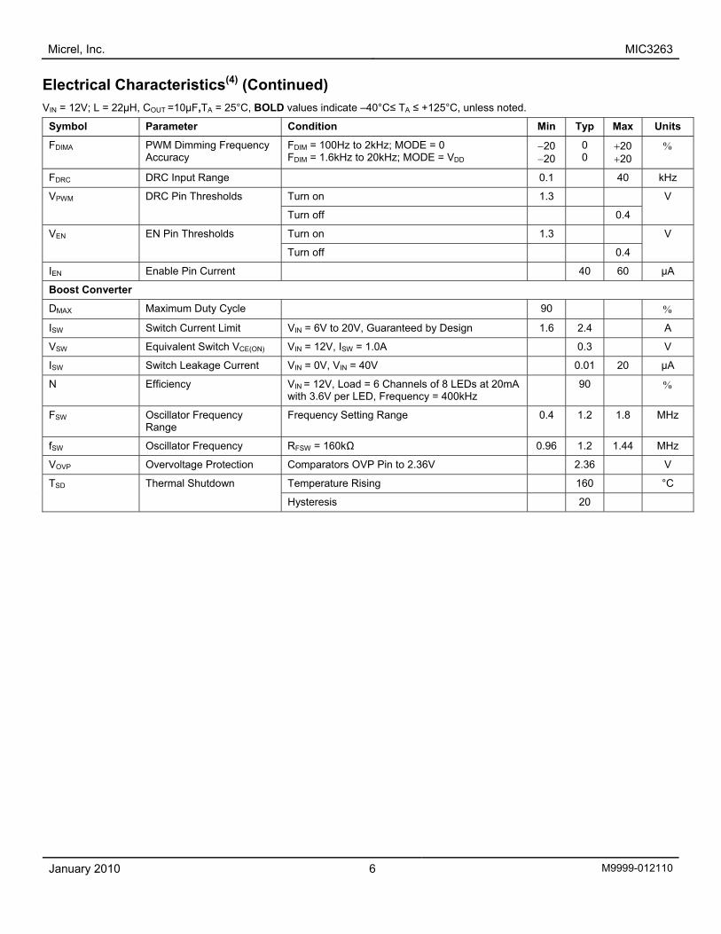
ectri teristics = 12V OLD values indicate –40°C≤ TJ ≤ +125°C, unless d.
Parameter Condition Min Typ Max Units
Absolute Maximum Ratings(1) Supply Voltage (VIN), Enable (VEN).................... .........+42V Supply Voltage (VIN).....................Switch Voltage (VSW)..................................... −0 V to +42V Enable (VEN) .................................Regulated Voltage (VDD) ................................. − .3V to 6V MODE (VMODE)..............................
)............................................................+
Over-Voltage Protection (VOVP) .................... −0 V to +42V DFS (VDFS
Switch Voltage (VOVPS) ................................. −0 V to +42V DRC (VDRC)...................................DFS Voltage (V ) ............................−0.3V to DFS
) −DD
RSLP (VRSLP ...................................... 0.3V to DDMODE Voltage (VMODE) ......................−0.3V to DDFSW Voltage (VFSW) ...........................−0.3V to DDDRC Voltage (VDR ) ...........................−0.3V to C
−DD
CRV Voltage (VCRV)............................ 0.3V to CINT Voltage (VCINT) ..........................−0.3V to ISET Voltage (VISET) ...........................−0.3V to Comp Voltage (VCOMP)........................−0.3V to IO1–IO6 Voltage (VIO1-IO6) .....AGND to PGND ................ ...Lead Temperature (soldering, 10 20s) ................... 260°C Storag emperatu ............−ES ing(3)..................... ..............................1.5kV
Operating Ratings(2)
El cal Charac (4) VIN ; L = 22μH, COUT =10μF,TA = 25°C, B note
Symbol
VIN Supply Voltage Range ix Ch nel 8 40 V 30mA 8 LEDs/Channel, All s an s
VIN ange 30mA 6 LEDs/Channel, All six Ch nels 6 40 V Supply Voltage R an
IVIN Not Switching, VOVP = 4V 6.5 10 mA Quiescent Current
VDDREG VDD Regulation V = 6V to 40V, I = 0mA to 6mA 4.5 5 5.5 IN DD
ISD Shutdown Current (DC 6.5 20 μA Pin Low) VEN = 0V
Current Control
IO1 IO ) Volt 30mA
e C ne s Us 1.2 V 6 Minimum IO (1–6operation to Sink
age for
Voltage on IO (1–6) if Only Onand ISET = 30mA
han l i ed
VOS Maximum Output VoltaOvershoot when Current
3 % ge 22μH, 10μF
Sources are OFF in PWM Dim Mode
I Channel Current Matching ILED = 30mA and Dimming RatiLEDMATCH o = 100% VIO = 1.2V on All Channels
−3 0 +3 %
ILEDSET Initial Current Setting Accuracy RSET = 2k ILED = 30mA
−2 −3
0 +2 +3
%
FDIMR PWM Dimming Frequency Adjust Range
MODE = 0V, RDFS = 400kΩ, Frequency = 100Hz MODE = 0V, RDFS = 32kΩ, Frequency = 1.2kHz MODE = VDD, RDFS = 400kΩ, Frequency = 1.6kHz MODE = VDD, RDFS = 32kΩ, Frequency = 20kHz
0.1 20 kHz
Notes: 1. Exceeding the absolute maximum rating may damage the device. 2. The device is not guaranteed to function outside its operating rating. 3. Devices are ESD sensitive. Handling precautions recommended. Human body model, 1.5k in series with 100pF. 4. Specification for packaged product only.
Micrel, Inc. MIC3263
January 2010 6 M9999-012110
IN 22 –40°C≤ TA ≤ + ted.
Symbol Parameter Min Typ Max Units
Electrical Characteristics(4) (Continued) V = 12V; L = μH, COUT =10μF,TA = 25°C, BOLD values indicate
Condition
125°C, unless no
FDIMA ming F quency FDIM = 100Hz to 2kHz; MODEFDIM = 1.6kHz to 20kHz; MOD DD 20
0 0
+20+20
% PWM Dim reAccuracy
= 0 E = V
−20 −
FDRC DRC Input Range 0.1 40 kHz
Turn on 1.3 VPWM DRC Pin Threshol
Turn off 0.4
V ds
Turn on 1.3 VEN EN Pin Thresholds
Turn off 0.4
V
I re 40 60 μA EN Enable Pin Cur nt
Boost Converter
DMAX ximum Duty C 90 % Ma ycle
ISW ent Li to 20V, Guaranteed b esi .6 2.4 A Switch Curr mit VIN = 6V y D gn 1
VSW witch VCE IN = 12V, ISW = 1.0A 0.3 V Equivalent S (ON) V
I ge C 40V 0.01 20 μA SW Switch Leaka urrent VIN = 0V, VIN =
N Efficiency VIN = 12V, Load = 6 Channels of 8 LEDs at 20mA with 3.6V per LED, Frequency
90 % = 400kHz
FSW Oscillator Frequency Range
Frequency Setting Range 0.4 1.2 1.8 MHz
fSW Oscillator Frequency RFSW = 160kΩ 0.96 1.2 1.44 MHz
VOVP Overvoltage Protection Comparators OVP Pin to 2.36V 2.36 V
Temperature Rising 160 °C TSD Thermal Shutdown
Hysteresis 20
Micrel, Inc. MIC3263
January 2010 7 M9999-012110
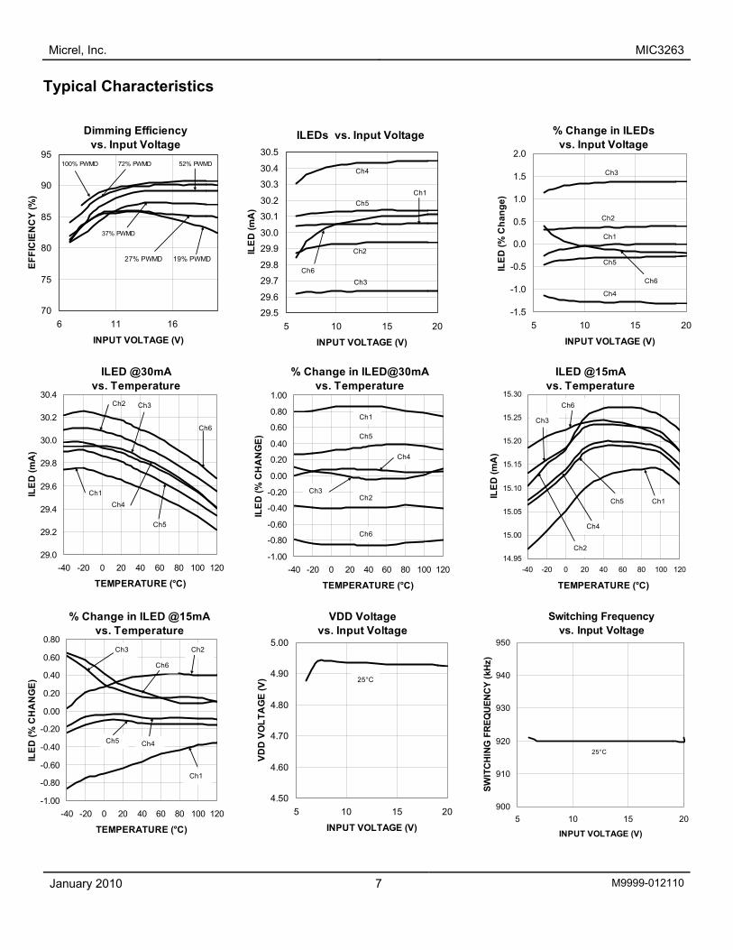
Typical Characteristics
Dimming Efficiency vs. Input Voltage
70
75
80
85
90
95
6 11 16
INPUT VOLTAGE (V)
100% PWMD 72% PWMD 52% PWMD
37% PWMD
27% PWMD 19% PWMD
%
-1.5
-1.0
-0.5
0.0
0.5
1.0
1.5
2.0
I
ILED
(% C
hang
e)
Change in ILEDs vs. Input Voltage
5 10 15 20
NPUT VOLTAGE (V)
Ch1
Ch2
Ch3
Ch4
Ch5
Ch6
ILEDs vs.
29.5
29.6
29.7
29.8
29.9
30.0
30.1
30.2
30.3
30.4
30.5
5 1
INPUT V
Ch1
Ch2
Ch3
Ch4
Ch5
Ch6
Input Voltage
0 15 20
OLTAGE (V)
EFFI
CIE
NC
Y (%
)
ILED
(mA
)
VDD Voltage vs. Input Voltage
4.50
4.60
4.70
4.80
4.90
5.00
5 10 15
INPUT VOLTAGE (V)
VDD
VO
LTA
GE
(V)
20
25°C
Switching Frequencyvs. Input Voltage
900
910
920
930
940
950
5 10 15 20
INPUT VOLTAGE (V)
SWIT
CH
ING
FR
EQU
ENC
Y (k
Hz)
25°C
ILED @15mA vs. Temperature
14.95
15.00
15.05
15.10
15.15
15.20
15.25
15.30
-40 -20 0 20 40 60 80 100 120
TEMPERATURE (°C)
ILED
(mA
)Ch1
Ch2
Ch3
Ch4
Ch5
Ch6
% Change in ILED@30mAvs. Temperature
-1.00
-0.80
-0.60
-0.40
-0.20
0.00
0.20
0.40
0.60
0.80
1.00
-40 -20 0 20 40 60 80 100 120
TEMPERATURE (°C)
ILED
(% C
HA
NG
E)
ILED @30mA vs. Temperature
29.0
29.2
29.4
29.6
29.8
30.0
30.2
30.4
-40 -20 0 20 40 60 80 100 120
TEMPERATURE (°C)
Ch1
Ch2 Ch3
Ch4
Ch5
Ch6
ILED
(mA
)
Ch1
Ch5
Ch4
Ch3Ch2
Ch6
% Change in ILED @15mAvs. Temperature
-1.00
-0.80
-0.60
-0.40
-0.20
0.00
0.20
0.40
0.60
0.80
-40 -20 0 20 40 60 80 100 120
TEMPERATURE (°C)
ILED
(% C
HA
NG
E)
Ch1
Ch2Ch3
Ch4Ch5
Ch6

Micrel, Inc. MIC3263
January 2010 8 M9999-012110
Functional Characteristics
V , V , I at 10% Dimming OUT SW LED
Dimming Transient Response
LED Ripple Current
Line Transient Response
Switching Waveform
Start Up
Micrel, Inc. MIC3263
January 2010 9 M9999-012110
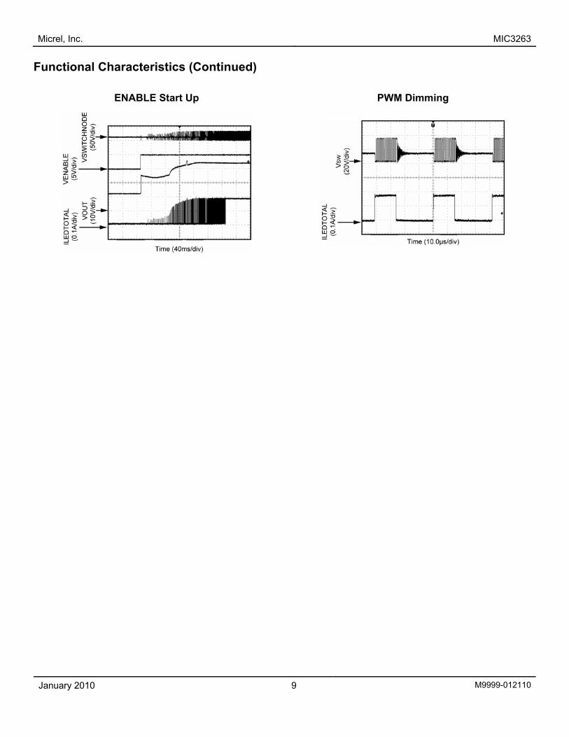
Functional Characteristics (Continued)
ENABLE Start Up
PWM Dimming

Micrel, Inc. MIC3263
January 2010 10 M9999-012110
Functional Diagram
Micrel, Inc. MIC3263
January 2010 11 M9999-012110
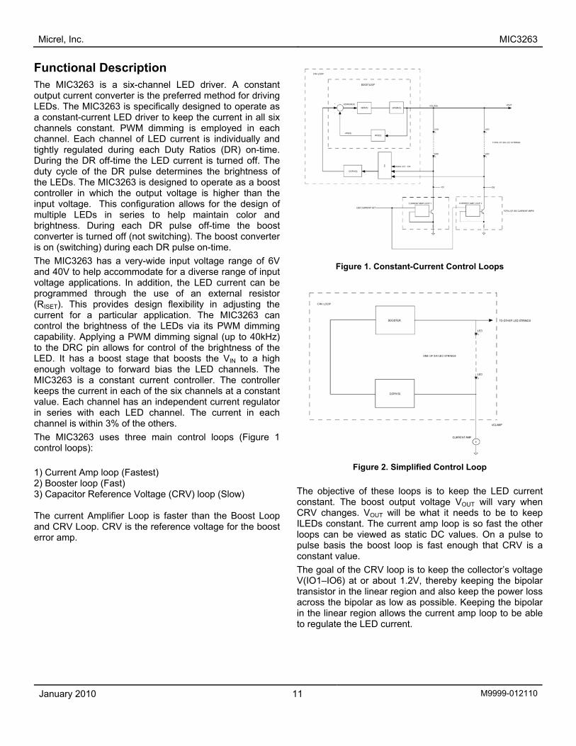
A constant d for driving operate as nt in all six
ed in each vidually and R) on-time. ed off. The ightness of as a boost er than the e design of
or a e boost st converter
range of 6V nge of input rent can be nal resistor djusting the IC3263 can M dimming
dimming signal (up to 40kHz) ness of the
s a boost stage that boosts the VIN to a high rd bias the LED channels. The
t current controller. The controller nnels at
value. Each channel has an independent currenen
The MIC3263 uses three main control loopscontrol loops): 1) Current Amp loop (Fastest) 2) Booster loop (Fast) 3) Capacitor Reference Voltage (CRV) loop (Slo The current Amplifier Loop is faster than the Boost Loop and CRV Loop. CRV is the reference voltage for the boost error amp.
Functional Description The MIC3263 is a six-channel LED driver. output current converter is the preferred methoLEDs. The MIC3263 is specifically designed toa constant-current LED driver to keep the currechannels constant. PWM dimming is employchannel. Each channel of LED current is inditightly regulated during each Duty Ratios (DDuring the DR off-time the LED current is turnduty cycle of the DR pulse determines the brthe LEDs. The MIC3263 is designed to operatecontroller in which the output voltage is highinput voltage. This configuration allows for thmultiple LEDs in series to help maintainbrightness. During each DR pulse off-timeconverter is turned off (not switching). The boois on (switching) during each DR pulse on-time.The MIC3263 has a very-wide input voltage and 40V to help accommodate for a diverse ravoltage applications. In addition, the LED curprogrammed through the use of an exter(RISET). This provides design flexibility in acurrent for a particular application. The Mcontrol the brightness of the LEDs via its PWcapability. Applying a PWM
colth
nd
to the DRC pin allows for control of the brightLED. It haenough voltage to forwa
onstan
MIC3263 is a ckeeps the current in each of the six cha a constant
t regulator t in each
(Figure 1
in series with each LED channel. The currchannel is within 3% of the others.
w)
Figure 1. Constant-Current Control Loops
Figure 2. Simplified C
The objective of these loops is tconstant.
ontrol Loop
o keep the LED current The boost output voltage VOUT will vary when
CRV changes. VOUT will be what it needs to be to keep ILEDs constant. The current amp loop is so fast the other loops can be viewed as static DC values. On a pulse to pulse basis the boost loop is fast enough that CRV is a constant value. The goal of the CRV loop is to keep the collector’s voltage V(IO1–IO6) at or about 1.2V, thereby keeping the bipolar transistor in the linear region and also keep the power loss across the bipolar as low as possible. Keeping the bipolar in the linear region allows the current amp loop to be able to regulate the LED current.

Micrel, Inc. MIC3263
January 2010 12 M9999-012110
r th ltage)
sed as the oost voltage
(V ) will decrease. With lower VOUT, V(IO) alsDischarging of CRV continues unt
vo
e
bo ill con
al dimming at the same dimming le
V 0% then
C o
spscy n ipt
rrss the cur
mge and the
the positive of the PWM comparator. The other input to the
PWM comparator is the error amp output (called VEA). The error amp’s negative input is the feedback voltage (VOVP). The OVP pin is used as the voltage feedback to the error amplifier. In this way the output voltage is regulated. If VOVP drops, VEA increases and therefore the power switch remains on longer so that VCS can increase to the level of VEA. The reverse occurs when VOVP increases. The output voltage is always higher than the input voltage. The external CRV (see C7 in Typical Application illustration) is used as the reference voltage to the boost error amp.
The boost regulated output voltage is:
Equation 1
V(IO) Too High If the collector voltage V(IO1–IO6) is greatethen the CRV loop will slowly discharge (lower the CRV capacitor. Since the CRV capacitor is ureference voltage for the boost error amp the b
than 1.2V, e vo
OUTdecreases.
o il V(IO) is
1.2V.
V(IO) Too Low If the collector voltage V(IO1-IO6) is less thCRV loop will slowly charge (increa
an 1.2V the ltage) the se the
CRV. Since CRV is used as the reference volboost converter’s error amp the boost voltagincrease. With higher VOUT, V(IO) also increaseof CRV continues until V(IO) is about 1.2V. These control loops operate as described aDR high pulses. When DR is low the booster islast state of the CRV charge or discharge wuntil the next DR pulse. If the external PWMpulse (DRC) is removed, the intern
tage for the (VOUT) will C g s. hargin
ve during off and the
tinue Dimming
pulse (DR) vel before loop will
will continue dimmingthe signal at DRC was removed and the CRkeep operating normally. If external PWM DIMcharge/discharge states will discontinue and longer be charged or discharged. CRV discharge through the circuitry connected to it
Boost Controller Operation The MIC3263 uses a peak current-mode booin its boost stage. The boost converter is a modulation (PWM) controller and operates thu(FF) is set on the leading edge of the clock the FF is set a gate driver drives the power bon. Current flows from VIN through the inducthrough the internal power switch and curesistor-to-PGND. The voltage acro
isRV will nwill slowly
t controller ulse width . A flip-flop cle. Wheolar switch or (L) and ent sense rent sense p (needed resistor is added to a slope compensation ra
for stability). The sum of the current-sense voltaslope compensation voltages (VCS) is fed into terminal
(R1+R2)V = CRV ×OUT R2
wide input voltage range, rrent-mode controller, the of superior line transient
design compensation. tion features, including:
) Current sensing for erload protection
Voltage Protection (OVP) output ver-voltage protection to prevent
operation above a safe upper limit (switching) during a
(not switching) low.
Application Information
t up, a switch connects 1.8V to the CRV. The stor divider (R1 and R2) is calculated to
oost output voltage with a VCRV of 1.8V.
Example:
50k R2 = 9.88k The CRV control loop will charge/discharge CRV until the correct boost voltage appears at the output.
Case 1 If 29.3V is too high to properly forward bias the LED channel at the ISET current level, then the current amp loop will decrease the drive to the bipolar transistor and V(IO) will increase and the CRV control loop will decrease CRV and the boost output voltage (VOUT) will decrease.
The MIC3263 is designed for afrom 6V to 40V. As a peak cuMIC3263 provides the benefits response as well as an easier toMIC3263 provides several protec
• Current Limit (ILIMITover current and ov
• Over-o
• The boost stage is onhigh DR pulse and is off when the DR pulse is
At Start Up At starfeedback resiachieve the approximate b
• 8 LEDs at 3.5V each = 28V• VIO = 1.2V • VOUT = 29.3V estimate• Set R divider to: R1 =1

Micrel, Inc. MIC3263
January 2010 13 M9999-012110
rcu
stor harder andntrol loop will increase CR
dn external pulse
the DRC pin. The duty cycle of the external pulsDRC) is converted to one of 16 levels called Duty Ratio(DR) (see Table 2 for DR ratios). It is this inte(DR) that is used to PWM dim the LEDs.
Case 2 If 29.3V is not high enough to properly forwaLED channel at the ISET current level, the loop will drive the bipolar transi
d bias the rrent amp V(IO) will V and the drop and the CRV co
boost output voltage (VOUT) will increase.
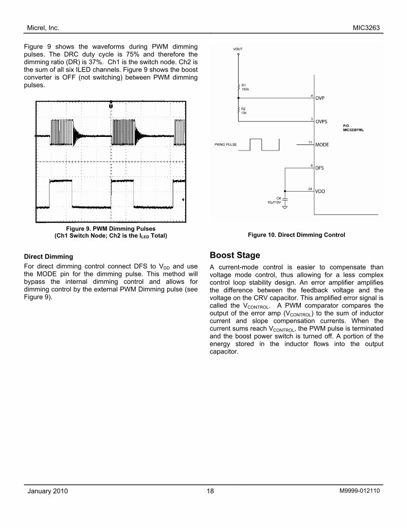
Internal Dimming Control In the internal dimming mode, the dimming isby the DFS and MODE pins. A
etermined is tied to
e (pulse at s
rnal pulse
Figure 3. Internal Dimming Control
External Dimming Control In external dimming mode, connect the DFS pin apply a PWM dimming pulse to the MODEexternal pulse directly controls the LED curre(see Figure 4).
to VDD and pin. The nt drivers
Figure 4. External Dimming Control
lts
pen, the voltage on the sistor (IO1-IO6) will go
rs the IO pins will detect less to the transistor. A flip-nd a power down and eset that channel. r, the channel of LEDs
e will be present at the r five channels will continue
ting normally. This fault sequence is identical if up to ur channels fail open or D channels will stay on
shorted, the voltage on stor (IO1–IO6) will go
at monitors the current ore than 7.5V at the
to the transistor will turn ondition. A power-down ed to reset that channel.
tolerate a two LED difference before a fault is detected.
e drive to the transistor, the channel of LEDs ce is present at the
channels will continue ce is identical if more
r channels fail open ED channels will stay on
tors the current amp bipolar transistor detects less than 0.5V at the collector (IO), then the base drive to the transistor will turn off. A flip-flop latches the fault condition. A power-down and power-up sequence is required to reset that channel. Without base drive to the transistor, the channel of LEDs will turn off and a high impedance is present at the collector (IO). The other five channels will continue operating normally. This fault sequence is identical if more than one LED channel fails open. If four channels fail open or short, then the remaining two LED channels will stay on and no more faults will be detected.
Fau
Open LED in Channel If any LED in a channel fails ocollector of the current amp tranlow. The circuitry that monitothan 0.5V and turn off base driveflop latches the fault condition apower up sequence is required to rWithout base drive to the transistowill turn off and a high impedanccollector (IO). The otheoperathree LED channels fail open. If foshort, then the remaining two LEand no more faults will be detected.
Short LED in Channel If any LED in a channel fails collector of the current amp transihigh in voltage. If the circuitry thamp bipolar transistor detects mcollector (IO), then the base drive off. A flip-flop latches the fault cand power-up sequence is requirA channel can
Without baswill turn off and a high impedancollector (IO). The other five operating normally. This fault sequenthan one LED channel fails open. If fouor short, then the remaining two Land no more faults will be detected.
Shorted Cathode (or IO Short) If the circuitry that moni
Micrel, Inc. MIC3263
January 2010 14 M9999-012110
OVP. OVP ccurs
aturnso, o. Foue on an chanopen), then
rmal for those three chann at t having to go through a po
pening (four or more ch
ost output VOUT_MA = 2.4*
5. Feedback VOVP will reach 2.4V and comparator will trip and turn off the boos
6. With the booster off, VOUT and VOVP will When feedback reduces to 1.7V the turned back on.
7. The OVP circuit will switch 1.8V onto CR8. If the load is still open the cycle will co
o Result
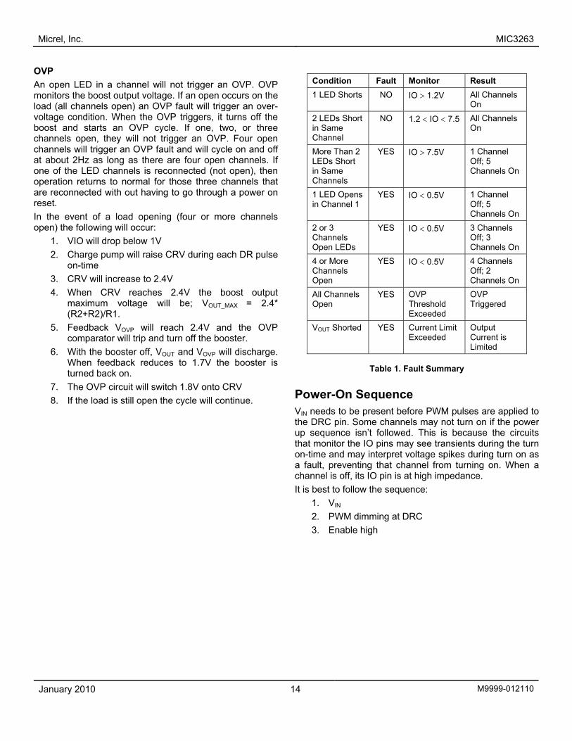
OVP An open LED in a channel will not trigger anmonitors the boost output voltage. If an open oload (all channels open) an OVP fault will trigger voltage condition. When the OVP triggers, it boost and starts an OVP cycle. If one, twchannels open, they will not trigger an OVPchannels will trigger an OVP fault and will cyclat about 2Hz as long as there are four open
on the n over- off the r three r open
d off nels. If
one of the LED channels is reconnected (not operation returns to no els th
wer on are reconnected with oureset.
he evenIn t t of a load o annels open) the following will occur:
1. VIO will drop below 1V . Charge 2 pump will raise CRV during each DR pulse
on-time 3. CRV will increase to 2.4V 4. When CRV reaches 2.4V the bo
maximum voltage will be; (R2+R2)/R1.
X
the OVP ter. discharge. booster is
V ntinue.
C ndition Fault Monitor 1 L > 1.2V All Channels
On ED Shorts NO IO
2 in Same
L t
Channel
< IO < 7.5 All Channels On
EDs Shor NO 1.2
MLEDs Short
o
in Same h
> 7.5V 1 Channel Off; 5 Channels On
re Than 2
C annels
YES IO
1 LED Opens C
< 0.5V 1 Channel Off; 5 Channels On
in hannel 1YES IO
2 or 3 h
Op
< 0.5V 3 Channels Off; 3 Channels On
C annels en LEDs
YES IO
4 oChOpen
IO < 0.5V 4 Channels Off; 2 Channels On
r More annels
YES
All Channels Open
YES OVP Threshold Exceeded
OVP Triggered
VOUT Shorted YES CurrenExceed
t Limit ed
Output Current is Limited
Table 1. Fault Su
mmary
n Sequence o be present before PWM pulses are applied to
DRC pin. Some channels may not turn on if the power up sequence isn’t followed. This is because the circuits that monitor the IO pins may see transients during the turn on-time and may interpret voltage spikes during turn on as a fault, preventing that channel from turning on. When a channel is off, its IO pin is at high impedance. It is best to follow the sequence:
1. VIN 2. PWM dimming at DRC 3. Enable high
Power-OVIN needs tthe

Micrel, Inc. MIC3263
January 2010 15 M9999-012110
Descriptions
t a resiGND to set the switching frequency between
400kHz and llowing equation ct RFSW
P p logy and
ub
s is a virtual ground of the resistor divider feedback ch connects
switch will open and disconnects the feedback resistor network
IN by the
his is the hat connects to the error amp input.
ency range. cy range is
D frequency elects High elects Low
Use the following equations to determine the value for
(kHz) + 432 (HF Mode)
(kHz) + 433 (LF Mode)
For a dimming frequency of 10kHz, use the HF Mode:
432 = 232kΩ in HF Mode
se LF Mode:
R (kΩ) = −335 × 1 + 433 = 98kΩ in LF Mode Use the closest standard value.
Figure 5. RDFS vs. Dimming Frequency in HF Mode
Figure 6. RDFS vs. Dimming Frequency in LF Mode
Pin
FSW Sets the boost switching frequency. Connecfrom FSW to
stor RDFS(kΩ) = −20 × fDIM
1.8MHz. Use the fo s to sele:
RFSW (kΩ) ≈ 500 − 0.3 × fSW(kHz)
RSLThe boost section is a peak current mode tyneeds slope compensation to eliminate soscillation (see “Slope Compensation”).
OVPS
o RDFS(kΩ) = −20 × 10 +
-harmonic For 1kHz, u
Thinetwork in the boost stage. At turn on, a switthis node-to-ground. When the part is disabled the
from ground. This eliminates current draw from Vboost resistor divider network.
OVP This is the over-voltage protection monitor. Alsofeedback signal t
t
MODE This selects the internal PWM dimming frequWhen mode is low the PWM dimming frequen100Hz to 2kHz. When mode is high the PWMrange is 1.5kHz to 20kHz. Mode is high sFrequency (HF) mode; Mode is low sFrequency (LF) mode.
DFS DFS stands for Dimming Frequency Select. Tfrequenc
he dimming y of the LEDs is different than the input dimmin
frequency at the DRC input. The MIC3263 uses n indimming frequency. This internal dimming frequency is programmable by an external resistor to ground RDFS. For direct dimming control, connect DFS to VDD and use the MODE pin for the input dimming pulse. This method by passes the internal dimming control and allows for dimming control by the external PWM pulse. When using internal dimming the range is determined by the MODE pin and the actual frequency is determined by RDFS. Connect a resistor to ground to select a dimming frequency.
g ternal a
RDFS:
RDFS(kΩ) = −335 × fDIM
Example:
DFS
RDFS(in kΩ) = -20*Dimming Frequency (in kHz) + 432
0
50
100
150
200
250
300
350
400
450
0 2.5 5 7.5 10 12.5 15 17.5 20 22.5
Dimming Frequency (kHz)
RD
FΩ
)S
(k
RDFS(kΩ) = -335*Dimming Frequency (in kHz) + 433
0
100
200
300
400
500
0 0.2 0.4 0.6 0.8 1 1.2 1.4
Dimming Frequency (kHz)
RD
FS(kΩ
)

Micrel, Inc. MIC3263
January 2010 16 M9999-012110
D ill be
is
nnect DFS to VDn for the input dimming pulse. This
or
un e a ing
tput of a transconductance differential am Rlein
efore, a RC filter is required to compensad
, a phase lead at the DFS pin. Ustor in series with a 2.2nF ceramic capac
h
nect a capacitor and resistor to ground to co
g Ratio Control (DRC) is an input PWM ming h
CINT integrates the DRC input pulse. For a PWM frequency range of around 1kHz use 100nF. For a PWM frequenrange of around 20kHz pulse, use 10nF. Fofrequency range of around 100Hz pulse use 1μF.
ISET Set the LED current of all six channels by this resistor. Use 2kΩ for 30mA and 3kΩ for 20mA. The RISET is inversely proportional to ILED. Use the following equation to find RISET:
The input frequency to the DRC pin can be 100Hz to 40kHz and the internal dimming frequency determined by RDFS.
R w
The duty cycle of the input frequency at DRC according to Table 2 for the actual dimming dutyFor direct dimming control, co
converted cycle. D and use method bythe MODE pi
passes the internal dimming control and dimming control by the external PWM.
DFS Filter In addition to the R resistor-to-gro
allows f
DFS d at thseries RC filter is required when operating frequencies below 1kHz. The reason is that thethe ou
DFS pin, a t dimmDFS pin is plifier. The
DFS is high differential amplifier has a high-frequency pole.At low dimming frequencies of around 1kHz around 100kΩ and the differential amplifier poa phase shift that can cause instabilities control.
produces the DFS
te for the ing a zero se a 4kΩ
itor. When e filter has
mpensate
Therlagging phase shift created by the pole by adand thereforeresiusing a dimming frequency of 2 kHz or less. Tno ill effect at higher dimming frequencies.
COMP Conthe boost stage.
DRC Dimmincon
dimtrol. The MIC3263 converts this to one
dimming ratios that is used to dim the LEDs. Tratio is built on a log scale.
CINT
of sixteen e dimming
cy r a PWM
LED
60R =ISET IΩ
best current matching accuracy design for an ILED current of 15mA to 30mA.
pin. This is used as the ge. The CRV capacitor is
continually being charged or discharged in order to keep VOUT at the right level (refer to Functional Diagram
o keep the IO’s at about
e linear-mode current t the cathode end of the
control loop will keep this he current amplifier is in can regulate the LED
ent number of LEDs in a ith the fewest LEDs will
as high as 7.5V before as a
er of LEDs in a channel nnels that have less
Ds biased correctly. A en channels can occur at monitors the IO pins off and that channel’s IO off channel’s IO pin will ut voltage. On a channel hannel’s IO voltage will
increase to keep correct voltage drops on the other series LEDs. It is best to use equal number of LEDs in each
rences in the LEDs ge drops so all IOs will not have the exact same
voltage. Each channel has its own monitoring circuit any V(IO) drops below
an LED opens), that channel is turned off and the other channels are unaffected. If any IO goes about 7.5V
short to VOUT), that channel is turned off and the other channels are unaffected.
VSW This is the boost-stage switch node, the collector of the internal power switch.
EN Connect EN high to enable the part, low to disable. Do not leave the EN pin floating.
VIN Supply voltage to the part (6V–40V).
For the
CRV Use a 2.2μF capacitor at the CRVreference voltage of the boost sta
illustration). CRV will be charged t1.2V.
IO1IO6 These are the connections to thamplifier in each channel. ConnecLED channels to these pins. The at about 1.2V. 1.2V insures that tthe linear region and therefore current. In cases where there are a differchannel, the V(IO) of the channel whave a higher V(IO). V(IO) can bethe fault monitoring circuits will sense that channelshort to VOUT. When there are a different numbthe IO voltage will be higher in the chaLEDs in order to keep the LEdifference of up to 7.5V betwebecause of this. If the circuits thsees a fault, that channel will turn pin will be at high impedance. Anbe near or below the booster outpthat has a shorted LED, that c
channel but there will always be diffevolta
monitoring the IO1IO6 pins. If0.5V (if
(if several LEDs

Micrel, Inc. MIC3263 VDD
January 2010 17 M9999-012110
This is the output of the internal LDO regulator. Connect a c capacitor to this pin.
e DRC input imming is a
feature of the MIC3263 which better matches the sensitivity of the human eye compared to linear dimming. The DRC le version is sin T le 2
C Duty ycle
P Dimming Ratio DR = 10(N − 1) / 7
10μF cerami
PWM Dimming The duty cycle of the PWM pulse applied to this converted to 16 log levels. This logarithmic dunique
duty-cyc.
to DR duty-cycle con hown ab
DRC
WM (DR) N
% % 0 0 0 1 6.25 1.0 2 12.5 1.4 3 18.75 1.9 4 25 2.7 5 31.25 3.7 6 37.5 5.2 7 43.75 7.2 8 50 10 9 56.25 14 10 19 62.5 11 68.75 27 12 75 37 13 81.25 52 14 87.5 72 15 93.75 100
Table 2. Dimming Ratio
To avoid skipping between dimming levels, theuses Flicker-Free Dimming control. This techniqdigital filter and hysteresis on the DRC pulse toclean DR output. The digital filter has a 0.1μF capacitor on the CINT pin to average the duty cycles of the PWM pulses. The averaged duty cycle has to be 4.16% higher than the nominal value before moving to the next dimming level as shown in Figure 7. Likewise, to move the previous dimming level the duty cycle has to be −4.16% lower than the nominal. To prevent flicker the duty-cycle hysteresis is set a 2%.
MIC3263 ue uses a provide a
Figure 7. Duty-Cycle Thresholds and Hysteresis
PWM Dimming Limits The minimum pulse width of the PWM Dim is determined by the PWM Dimming frequency and the L and C used in the boost stages output filter. At low-PWM Dimming frequencies, higher dimming ratios can be achieved:
TPWMDDim Ratio =TLEDON
Figure 8. PWM Dimming Ratio
perceive light flicker at a 00Hz. At 100Hz the time PWM dimming minimum
Consider that the human eye will PWM dimming frequency below 1between pulses is 10μs. If the pulse width is 5μs, then:
10msDim Ratio = = 2000/1
5μs
If high dimming ratios are required, a lower dimming frequency is required. During each DR pulse, the inductor current has to ramp up to it steady state value to generate the necessary boost output voltage in order for the full programmed LED current to flow in the LED channels. The smaller the inductance value the faster this time is and a narrower PWM dimming pulse can be achieved. But smaller inductance means higher ripple current.
Micrel, Inc. MIC3263
January 2010 18 M9999-012110
M dimming erefore the ode. Ch2 is
m of all six ILED channels. Figure 9 shows the boost converter is OFF (not switching) between PWM dimming pulses.
Figure 9 shows the waveforms during PWpulses. The DRC duty cycle is 75% and thdimming ratio (DR) is 37%. Ch1 is the switch nthe su
)
D and use ethod will
allows fo
Figure 9. PWM Dimming Pulses (Ch1 Switch Node; Ch2 is the I TotaLED l
Direct Dimming For direct dimming control connect DFS to VDthe MODE pin for the dimming pulse. This mbypass the internal dimming control and r dimming control by the external PWM Dimming ulse (see Figure 9).
p
Figure 10. Direct Dimm
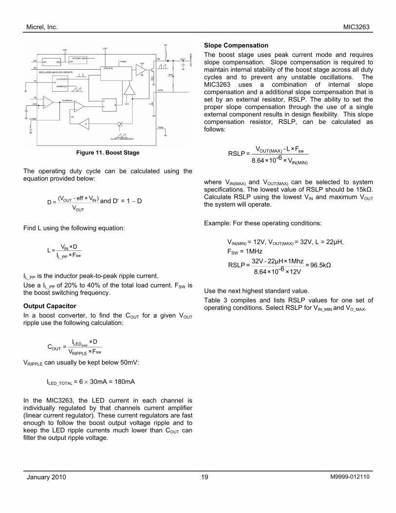
Boost Stage A current-mode control is easivoltage mode control, thus allow
ing Control
er to compensate than ing for a less complex
control loop stability design. An error amplifier amplifies the difference between the feedback voltage and the voltage on the CRV capacitor. This amplified error signal is called the VCONTROL. A PWM comparator compares the output of the error amp (VCONTROL) to the sum of inductor current and slope compensation currents. When the current sums reach VCONTROL, the PWM pulse is terminated and the boost power switch is turned off. A portion of the energy stored in the inductor flows into the output capacitor.
Micrel, Inc. MIC3263
January 2010 19 M9999-012110
Figure 11. Boost Stage The operating duty cycle can be calculated using the
equation provided below:
OUT IN
OUT
(V - eff × V )D =
Vand D′ = 1 − D
Find L using the following equation:
INswL_PP
L =I ×F
V ×D
IL_PP is the inductor peak-to-peak ripple current. Use a I SW is
Outpgiven VOUT
L_PP of 20% to 40% of the total load current. Fthe boost switching frequency.
ut Capacitor In a boost converter, to find the COUT for a ripple use the following calculation:
totalLEDOUT
RIPPLE
I ×DC =
V ×
swF
VRIPPLE can usually be kept below 50mV:
ILED_TOTAL = 6 × 30mA = 180mA In the MIC3263, the LED current in each channel is individually regulated by that channels current amplifier (linear current regulator). These current regulators are fast enough to follow the boost output voltage ripple and to keep the LED ripple currents much lower than COUT can filter the output ripple voltage.
ode and requires ensation is required to st stage across all duty
table oscillations. The n of internal slope
compensation that is . The ability to set the
proper slope compensation through the use of a single external component results in design flexibility. This slope compensation resistor, RSLP, can be calculated as follows:
Slope Compensation The boost stage uses peak current mslope compensation. Slope compmaintain internal stability of the boocycles and to prevent any unsMIC3263 uses a combinatiocompensation and a additional slope set by an external resistor, RSLP
OUT(MAX) sV -L×FRSLP = -68.64×10 × V
w
IN(MIN)
IN(MAX) OUT(MAX) can be selected to system
ficatio value of RSLP should be 15kΩ. e lowest VIN and maximum VOUT
will operate. Example: For these operating conditions:
2V, L = 22μH, FSW = 1MHz
where V and Vspeci ns. The lowest
lculate RSLP using thCathe system
VIN(MIN) = 12V, VOUT(MAX) = 3
32V - 22μH×1MhzRSLP = = 96.5kΩ-68.64×10 ×12V
Use the next highest standard value. Table 3 compiles and lists RSLP values for one set of operating conditions. Select RSLP for VIN_MIN and VO_MAX.

Micrel, Inc. MIC3263
January 2010 20 M9999-012110
VIN = OUT 12V, V = 32V 8.2 22μH μH 10μH F(kH
S RSLP z)
R LP RSLP 400 E . 2.24E+05 2.77 +05 2 70E+05 500 E . 2.03E+05 2.69 +05 2 60E+05 600 E . 1.81E+05 2.61 +05 2 51E+05 700 E .4 1.60E+05 2.53 +05 2 1E+05800 E .3 1.39E+05 2.45 +05 2 1E+05900 E .2 1.18E 2.37 +05 2 2E+05 +05
100 E .1 9640 2.30 +05 2 2E+05 51 110 E .0 75231 0 2.22 +05 2 3E+05120 E .9 5400 2.14 +05 1 3E+05 12 130 E .8 3270 2.06 +05 1 3E+05 93 1400 1.98E+05 1.74E+05 15000 1500 .64E+05 15000 1.90E+05 11600 1.82E+05 1.54E+05 15000 1700 1.74E+05 1.45E+05 15000 1800 1.66E+05 1.35E+05 15000
Table 3. RSLC Values
Boost Compensation Current-mode control simplifies the compensation. In current mode the double pole created by the output L and C is reduced to a single pole. The explanation for this is beyond the scope of this data sheet, but it can be thought because the inductor current becomes a cosou
nstant current rce and can’t act to change phase.
Figure 12. MIC3263 Current-Mode Loop Diagram
From the small signal block diagram the loop transfer function is:
Figure 13. Simplified Voltage Control Loop
Equation 2:
T(s) = Gea(s) × GVC(s) × H(s) where:
CRV
OUT
VH(s) =
V and
⎛ ⎞⎛ ⎞⎜ ⎟⎜ ⎟
⎝ ⎠⎝ ⎠ea m COMP
COMP
II 1
G (s) = g Z R +o sC
Equation 3:
( )( )⎛ ⎞⎜⎜
sL1- 2 ⎟⎟⎠⎛ ⎞⎛ ⎞ ⎝
⎜ ⎟⎜ ⎟ ⎞⎛⎝ ⎠⎝ ⎠⎝ ⎠
OUTvc
CONTROL
AD
OUT
V sG (s) =
V s
C2
where
⎜ ⎟
LOLOAD
LOAD
D' RD'R1=sRRi 2 1+
OUTLOAD
OUT
VR =
I and
Ai = 20 RCS = 0.02Ω AI and RCS are quantities that are internal to the MIC3263. The equation for GVC(S) is a theoretical model and should give an approximate idea of where the poles and zeros are located.
Ri = Ai ×Rcs = 0.4Ω .

Micrel, Inc. MIC3263
January 2010 21 M9999-012110
3 shows that Equation LOAD2D' R
s =L
is a right-half plane
PZ): Equa
zero (fRH
tion 4:
RHP Zero→ LOADRHPZ
2D' Rf =
2πL
The loop bandwidth should be about 1/10 of t
th t there is his greatly
fer function nalyzer. source. Tie will operate g CRV to a
nt DC voltage, this effectively opens the CRV control loop and allows the measurement of the boost control loop. GVC(S) can be calculated with a using the above equation. From the bode plot of GVC(S) find what the gain of VC(s) is at 1/10 of fRHPZ or t design the error amp gain GEA(s) so the loop gcross over frequency T(fCO) is 0db where fCO =1or lower.
Figure 14. Error Amp Transfer Function
The error amp is a gm type and the gain – GEA(S) – is: Equation 5:
he fRHPZ to ensure stability. From Equation 3, it is shown only the single pole due to RLOADCOUT. Tsimplifies the compensation. One needs only to get a bode plot of the transof the control to output GVC(S) with a network aTo measure GVC(S), tie CRV to a DC voltageCRV to the steady state voltage that CRV usually between 1V and 2.4V. By connectinconsta
a
computer
G less. Nexain at the
/10 of fRHPZ
Error Amp
⎛ ⎞⎛ ⎞⎜ ⎟⎜ ⎟
⎝⎝
gm = 0.056mA/V and ZO = 5MΩ. T
⎠⎠ea m COMP
COMP
II 1
G (s) = g Z R +o sC
he error amplifier zero is
COMP COMP
1f =Zero 2πR C
. Set the fCO at the mid band
where GEA(fCO) = gm × RCOMP. At fZERO × 10 the phase boost is near its maximum.
-100
-80
-60
-40
-20
Figure 15. Internal Error Amp and External Compensation
le 1 Conditions: VIN = 12V, VOUT = 29V, IOUT = 0.18A, L = 22μH, COUT = 4.7μF R = VOUT/IOUT = 161Ω. When VCRV = 1.8V, the is:
Examp
LOAD
RHPZf
LOADRHPZ
2D' Rf = = 162kH
2πL z
Figure 16 shows a plot of:
( )( )⎛ ⎞⎜ ⎟⎜ ⎟⎛ ⎞⎛ ⎞ ⎝ ⎠
⎜ ⎟⎜ ⎟ ⎛ ⎞⎝ ⎠⎝ ⎠⎜ ⎟⎝ ⎠
OUTvc
CONTROL
LOADLOAD
LOAD OUT
V sG (s) =
V s
sL1- 2D' RD'R1=sR CRi 2 1+
2
0
20
40
1.E+02 1.E+03 1.E+04 1.E+05 1.E+06Freq
Gai
n (d
b) p
hase
(deg
)
Gain
Phase
Midband Gain
Fzero

Micrel, Inc. MIC3263
January 2010 22 M9999-012110
-2001.E+02 1.E+03
-150
-100
-50
0
50
100
1.E+04 1.E+05 1.E+06
Freq
Gai
n (d
b) p
hase
(deg
)
GainPhase
26db
-40
-20
0
20
40
60
80
100
1.E+02 1.E+03 1.E+04 1.E+05 1.E+06Freq
Gai
n (d
b) p
hase
(deg
)
GainPhase Fco=1.6kHz
This example illustrates the RHPZ at 162kHz. details the −90° phase shift due to the RHPZ.
in (GVC)
The goal is to make the loop transfer function T(fCO) crossover well before the RHPZ.
Chose a
Figure 16
Figure 16. Control-to-Output Ga
RHPZco
ff =10
or less; chose
From the plot and or calculation, the magnitude of:---
cof = 16kHz .
G (16kHz) = 26dbvc
⎛ ⎞⎜ ⎟⎝ ⎠
1.8VH(s) = 20Log = -24db
29V
From:
T(s) = G (s) * G (s) * H(s)ea vc
T(16kHz) = G (16kHz) + 26db - 24db = 0ea
→G (16kHz) = -2db 0.8v/vea
e error amplifier’s zero at nF. The location of the
RO affects the phase boost in the loop transfer function. If fZERO were closer to 16kHz the phase boost would be less and vise versa.
Figure 17. Error Amp Gain and Phase (in Example 1)
Figure 18. Loop Gain and Phase (in Example 1)
Therefore R4 = 15kΩ. Next set thabout 5kHz. Therefore C2 = 2.2fZE
-100
( ) ≅ 0.8 = g Z II R g * Rm o m4 4
-80
-60
-40
-20
0
20
40
1.E+02 1.E+03 1.E+04 1.E+05 1.E+06Freq
Gai
n (d
b) p
hase
(deg
)
Midband Gain
Fzero
GainPhase
Micrel, Inc. MIC3263
January 2010 23 M9999-012110
r ermbol eter Minimum ominal Maximum Units
Design P ocedure for a LED Driv Sy Param N Input VIN Input Voltage 8 12 14 V I IN Input Current Output LEDs 8/Channel /Channel 8/Channel Number of LEDs 8Chs r of Channels 6 6 Channels Numbe 6 V F Forward Voltage of LED .4 3.6 4.0 V 3VIO e Drop at the IO Pin 1.1 1.2 2 VoltagVOUT Output Voltage 28 30 34 V ILED/ch el 30 30 mA LED Current/Chann 30 IOUT 0.18 A POUT r 6.2 W Output PoweDIM IN PWM Dimming 1 100 % FDIM Dimming Frequency (internal) 5 kHz OVP Output Over-Voltage Protectio 40 V n
FSW Switching Frequency 1 MHz eff Efficiency 80 85 % VDIODE Forward Drop of Schottky Diode 0.5 V
Design Example In this example, a boost six-channel LED driveoperating off a 12V input is being de gned. This esign has been created to drive six channels oLEDs/channels for a total of 48 LEDs. The LED cu
% minimum
Let R2=150k,
r si d
f eight rrent
will be set at 30mA. One is designing for 80efficiency at a switching frequency of 1MHz. For 34V out:
CRV
OUT CRV
V ×R2 1.8V ×150kΩR1= = = 8.39kΩV - V 34V -1.8V
Therefore: VOVP= 2.4* (R2+R2)/R1=45V. 45V is too high, meaning VCRV has to operate at a higher voltage than 1.8V. The CRV loop will charge the CRV capacitor to the necessary voltage to regulate.
Let VCRV = 2.2V therefore:
CRV
OUT CRV
V ×R2 2.2V ×150kΩR1= = = 10.4kΩ
V - V 34V - 2.2V
Use the closest standard value of 10.5kΩ.
efore:
VOVP = 2.4* (R2+R2)/R1 = 40V
Select RISET for a Given ILED
Ther
ISETLED
60 60R = Ω = = 2 ΩI 30mA
k
Use 2kΩ for RISET (R9)

Micrel, Inc. MIC3263 Switching Frequency Set RFSW
January 2010 24 M9999-012110
To fi t following equatio
)
00 − 0.3 × (1000) = 200kΩ
Dim n c tor RDFS FDIM ode is used. Connect MODE to VDD. To find RDFS (R8) use the following equation:
DIM
e 10 ency DR will
t Dd according to Table 2 for the actual d
ming frequency is high the filter R6 is not necessary. They may be used with no ill effe
Operating Duty Cycle The operating duty cycle can be calculatedEquation 6. Equation 6:
nd he value of RFSW use the n:
RFSW(kΩ) ≈ 500 − 0.3 × fSW(kHz
R (kΩ) ≈ 5FSW
Use 200kHz for RFSW (R5).
mi g Frequency Sele t Resis is 5kHz therefore HF m
RDFS(in kΩ) = 432 − 20 × F (in kHz) = 432 − 20 × 10 = 232(kΩ)
The input frequency to the DRC pin can b40kHz and the internal dimming frequ
0Hz to
always be 5kHz. The duty cycle of the input frequency aconverte
RC is imming
and C6 ct.
using
duty cycle. Since the dim
( )OUT(NOM) IN(NOM)NOM
V - eff × VD =
OUT(NOM)V
( )×OUT(MAX) IN(MAX)MAX
OUT(MAX)
V - eff VD =
V
( )×OUT(MAX) IN(MAX)MIN
OUT(MAX)
V - eff VD =
V
Therefore DNOM = 66%, DMAX = 80% and DMIN = 58%.
ominal, minimum, m given the operating n example table. The
ue of the RMS input current is necessary to ensure proper operation. Using Equation 7, the following values have been calculated: Equation 7:
Inductor Selection First calculate the RMS input current (nand maximum) for the systeconditions listed in the desigminimum val
OUT(MIN) OUT(MIN)IN_RMS(MAX) (RMS)
IN(MAX)
=V ×I
I = 0.43Aeff × V
OUT(NOM) OUT(NOM)IN_RMS(NOM) (RMS)
IN(NOM)
V ×II = = 0.53A
eff × V
OUT(MAX) OUT(MAX)IN_RMS(MIN)I =
eff × V (RMS)IN(MIN)
V × I= 0.9A
al
eak-to-peak) IL_PP to be ax), in this case 40%, we
.4 × 0.9 = 0.36APP
There is a trade off between the inductor value and the minimum PWM dimming pulse. The larger the inductor, the longer the PWM dimming pulse time will be. Due to this, the percentage of the ripple current may be limited by the required PWM dimming pulse. Also, the internal current amplifiers will attenuate the LED ripple current by more than a magnitude. It is recommended to operate in the continuous conduction mode. The value of “L” in Equation 8 represents Continuous Conduction Mode. Equation 8:
IOUT is the same as ILED tot
Selecting the inductor current (pbetween 20% to 50% of IIN_RMS(mobtain: IL_PP(MAX) = 0.40 × IIN_RMS(MAX) = 0
IN
L_PP SW
V ×DL =
I ×F

Micrel, Inc. MIC3263
January 2010 25 M9999-012110
Using the nominal values, one gets:
12V × 0.66L = = 22μH
0.36A ×1MHz
t a standard value, use the next higher stvalue. Select the standard inductor value of 22µHGoing back and calculating the actual ripple current gives:
If no andard
.
IN(NOM) NOML_PP
SW
V ×D 12V × 0.66I = = = 0.3
L ×F 22μH×1MHz
PP6A
The average input current is different than the RMS input ecause of the ripple current. If the ripple current
is low, then the average input current nearly equals the RMS input current. In the case wh re the average input current is different than the RMS, Equation 9 shows the following:
current b
e
Equation 9:
( ) ( )IN_PPIII =N_AVE(MAX) IN_RMS(MAX)
2I2-
12
( ) ( )≈IN_AVE(MAX)
20.362
I = 0.9 - 0.9A
found
Equation 10:
IL_PK(MAX) = IIN_AVE(MAX) + 0.5 ×IL_PP(MAX) = 1.0A The saturation current (ISAT) at the highest operating temperature the inductor must be rated higher than this. The power dissipated in the inductor is: Equation 11:
PINDUCTOR(max) = IIN_RMS(MAX)2 × DCR
t # DO3316P-223ML is used in this example. Its DCR is 85 m
2 5 mΩ = 67mW
e ILED ripple current is a impo r compared to that of the output
hough the two are directly related). To find the COUT for a required ILED ripple use the following calculation: For an output ripple ILED(RIPPLE) = 20mA. Equation 12:
12The Maximum Peak input current IL_PK can using Equation 10:
A CoilcrafΩ, ISAT =2.6A.
PINDUCTOR(MAX) = 0.9 × 8
Output Capacitor In this LED driver application, thmore rtant factoripple voltage (alt
LEDOUTC = (total)
swRipple
I ×D
V ×F
V PPLE can usually be kept below 50mV:
0mA
RI
ILED(total) = 6 × 30mA = 18
OUT0.18A × 0.76
C = = 2.7μF50mV ×1Mhz
arge depends upon the luses and the size of the
se COUT full output voltage VOUT
flows.
put Capacitor The input capacitor is shown in the Typical Application. For superior performance, ceramic capacitors should be used because of their low Equivalent Series Resistance (ESR). The input capacitor C ripple current is equal to the ripple in the inductor. The ripple voltage across the input capacitor, is the ESR of CIN times the inductor ripple. The input capacitor will also bypass the EMI generated by the converter as well as any voltage spikes generated by the inductance of the input line. For a required VIN(RIPPLE). Equation 13:
Use 2.7µF or higher. The amount that COUT will dischtime between PWM Dimming poutput capacitor. At the next PWM Dimming pulhas to be charged up to the before the desired LED current
In
IN
( )IN_PPIN
FIN(RIPPLE) SW
I 0.36AC = = = 0.8μF
8 × V × 8 × 50mV ×1MHz

Micrel, Inc. MIC3263
January 2010 26 M9999-012110
ed. Tooot, a
citance may be required. Use
of the lower ry time. The
tress on the diode is the maximum VOUT and a diode with a higher rating than maximum
OUT ld be used. An 80% de-rating is recommended here as well.
14:
_(MAX OUT 0.18A
Equation 15:
VDIODE × IDIODE_(MAX)
s 0.5
0.5V × 0.18A≈ 0.09W
er Losses To find the power losses in the MIC3263: There is25mA to 35m npu to t VDD pin. The internal switch has an CE(ON MAX) o0.5V.
Equation 16:
PMIC3263(MAX) = VIN(MAX) × 35mA + PWRSW(MAX)
Where PWRSW(MAX) is the power loss of the internal bipolar power switch. The power switch power losses are the sum of the on-time losses; PWRSW(MAX) and the switching losses: PWRSW(SWITCHING MAX). PWRSW(MAX) = PWRSW(MAX) + PWRSW(SWITCHING MAX)
Equation 17:
This is the minimum value that should be usprotect the IC from inductive spikes or any oversh
larger value of input capa2.2µF or higher as a good safe min.
Rectifier Diode Selection A Schottky diode is best used here because forward voltage and the low reverse recovevoltage stherefore, V shou
Equation
IDIODE ) = I (MAX) =
PDIODE(MAX) ≈ A SK34A is used in this example, it’s VDIODE i
V.
about
PDIODE(MAX) ≈
MIC3263 Pow
A i t from VIN in he bipolar power V f about
VCE(ON MAX) ≈ 0.5V
SW_ON( MAX) SW_RMS(MAX) CE_ON_RMS (MAX)PWR = I × V
( )⎛ ⎞⎜ ⎟⎜ ⎟⎜ ⎟⎝ ⎠
≈
IN_PP(MAX) IN_AVE(MAX)SW_RMS(MAX)
(MAX) IN_AVE(MAX)
I2I2I = D × +
12
D ×I
CE_ON_RMS (MAX) (MAX) CE_ON( MAX)V = D × V
SW_ON( MAX) (MAX) AVE(MAX) CE_ON (MAX)PWR = D ×I × V
SW_ON( MAX)PWR = 0.8 × 0.9A × 0.5V = 0.36W
Equation 18:
al power switch on an off transition time
A + 0.97 = 1.46W
resent at VSW, a snubber may be needed. A snubber is a damping resistor in series with a DC blocking capacitor in parallel with the power switch. When the power switch turns off, the drain to source capacitance and parasitic inductance will cause a frequency ringing at the switch node. A snubber circuit as shown in the application schematics may be required if ringing is present at the switch node. A critically damped circuit at the switch node is where R equals the characteristic impedance of the switch node. Equation 18:
SW_SWITCHING (MAX OUT(MAX) IN_AVE(MAX) swPWR = V ×I × tsw ×F)
tsw ≈ 20ns is the intern
SW_SWITCHING (MAX)PWR = 34V ×0.9×
Therefore:
PMIC3263(MAX) = 14V × 35m
Snubber If a high-frequency ringing is p
20ns×1MHz = 0.61W
high
PARISITICSNUBBER
DS
LR =
C

Micrel, Inc. MIC3263
January 2010 27 M9999-012110
he bshee
SNUBBER ≈ 2Ω ½ W and CSNUBBER ≈ 470pF to 100a snubber is used, the power dissipation in the R is:
SNUBBER SNUBBER OUT SW
PSNUBBER = 470pF × 34V2 × 1MHz = 0.54W Tabl e powe s in the Design Exam
The explanation of the method to find tsnubber is beyond the scope of this data R
est R t. Use 0pF. If
SNUBBER
R = C × V 2 × F
e 2 illustrates th r losseple.
Description Value Power Loss in the L 0.069W P iode ower Loss in the Schottky D 0.09W MIC3263 Power Loss 1.46W Maximum Total Losses 1.62W Minimum Efficiency 80%
Table 2. Major Power Losses
ge that the OVP will trigger is set according to Equation 19. Using the values for this example gives a max output voltage of:
RSLP To find RSLP use Equation 1 (which is repeated here): Use the minimum VIN and the maximum VOUT.
OVP The output volta
Equation 19:
VOVP= 2.4× (R2+R2)/R1=40V
OUT(MAX) sw
IN(MIN)
V - L ×FRSLP = -68.64 ×10 × V
In this example:
34 - 22μH×1MhzRSLP = = 174kΩ-68.64 ×10 × 8

Micrel, Inc. MIC3263
January 2010 28 M9999-012110
Evaluation Board Schematic

Micrel, Inc. MIC3263
January 2010 29 M9999-012110
B f MatNumber Ma turer Description Qty.
ill o erials Item Part nufac
C1 OPEN 0603ZC222KAT AVX(1) 2A C1608X7R1H222K TDK(2) C2, C6
222K muRata(3)
, 10V, X7R, 0603 2
GRM188R71H
2200pF
C5750X7R1H106M TDK(2) C3, C8
6KAZ2A AVX(1) 10μF, 50V, X7R, 2220 2
22205C10GRM21BR71A106KE51L muRata(3)
C4 6KAT2 (1)
10μF, 10V, 0805 1 0805ZD10 A AVX0603YC104KAT2A AVX(1) C1608X7R1C104K TDK(2) C5
71C1
0.1μF, 16V, X7R, 0603 1
GRM188R 04K muRata(3) 0603ZD225KAT2A AVX(1)
GRM188R61A225 ta(3) KE34D muRaC7
C1608X5R1A2 K(2)
2.2μF, 10V, X5R, 0603 1
25K TDSK34A MCC (4)
D1 B349LA-13 nc.
hottky 3A, 40V (SMA) 1 Diode, I (5) Sc
L1 23 aft(6) 22μH, 2.6A 1 DO3316P-2 ML CoilcrR1 0K i ale(7) 150k 2 CRCW060315 FKEA V shay DR2 K0 i ale(7) 10k 1 CRCW060310 FKEA V shay DR3 110KK i 1 CRCW0603 FKEA V shay Dale(7) 110k (RSLP) R4 CRCW060315K0FKEA Vishay Dale(7) 15.0k, 0603 (RCOMP) 1 R6 CRCW060340K2FKEA Vishay Dale(7) 4.02k R5 CRCW0603200KFKEA Vishay Dale(7) 200k 1 R7 CRCW0603100KFKEA. Vishay Dale(7) 100k 1 R8 CRCW060326K7FKEA Vishay Dale(7) 97.6k 1 R9 CRCW06032K00FKEA. Vishay Dale(7) 2k 1 U1 MIC3263YML Micrel, Inc.(8) Six-Channel WLED Driver for Backlighting Applications 1
Notes: 1. AVX: www.avx.com. 2. TDK: www.tdk.com. 3. Murata Tel: www.murata.com. 4. MCC: www.mccsemi.com. 5. Diode, Inc.: www.diodes.com. 6. Coilcraft: www.coilcraft.com. 7. Vishay: www.vishay.com. 8. Micrel, Inc.: www.micrel.com.

Micrel, Inc. MIC3263
January 2010 30 M9999-012110
Evaluation Board PCB Layout

Micrel, Inc. MIC3263
January 2010 31 M9999-012110
Package Information
24-Pin 4mm x 4mm (MLF®)

Micrel, Inc. MIC3263
January 2010 32 M9999-012110
Recommended Land Pattern
MICREL, INC. 2180 FORTUNE DRIVE SAN JOSE, CA 95131 USA TEL +1 (408) 944-0800 FAX +1 (408) 474-1000 WEB http://www.micrel.com
The information furnished by Micrel in this data sheet is believed to be accurate and reliable. However, no responsibility is assumed by Micrel for its
use. Micrel reserves the right to change circuitry and specifications at any time without notification to the customer.
Micrel Products are not designed or authorized for use as components in life support appliances, devices or systems where malfunction of a product can reasonably be expected to result in personal injury. Life support devices or systems are devices or systems that (a) are intended for surgical implant
into the body or (b) support or sustain life, and whose failure to perform can be reasonably expected to result in a significant injury to the user. A Purchaser’s use or sale of Micrel Products for use in life support appliances, devices or systems is a Purchaser’s own risk and Purchaser agrees to fully
indemnify Micrel for any damages resulting from such use or sale.
© 2010 Micrel, Incorporated.


![[0.96]Low-Speed Performance Improvement of Direct Torque](https://cdn.vdocument.in/doc/165x107/61c1db76fa862d0b660713f1/096low-speed-performance-improvement-of-direct-torque-.jpg)


