Download - SMART SENSORS BASED ON INTEGRATED OPTICS

REPORT DOCUMENTATION PAGE Form Approved
OMB NO. 0704-0188
Public Reporting burden for this collection of information is estimated to average 1 hour per response, including the time for reviewing instructions, searching existing data sources, gathering and maintaining the data needed, and completing and reviewing the collection of information. Send comment regarding this burden estimates or any other aspect of this collection of information, including suggestions for reducing this burden, to Washington Headquarters Services, Directorate for information Operations and Reports, 1215 Jefferson Davis Highway, Suite 1204, Arlington, VA 22202-4302, and to the Office of Management and Budget, Paperwork Reduction Project (0704-0188.) Washington, DC 20503. 1. AGENCY USE ONLY (Leave Blank) 2. REPORT DATE
21 July 2003
3. REPORT TYPE AND DATES COVERED
Final Technical Report 1 September 1998 through 31 May 2003
4. TITLE AND SUBTITLE
Smart Sensors Based on Integrated Optics and Microelectromechanical Systems
5. FUNDING NUMBERS
DAAG55-98-1-0477
AUTHOR(S) Tristan J. Tayag
7. PERFORMING ORGANIZATION NAME(S) AND ADDRESS(ES)
Texas Christian University Department of Engineering TCU Box 298640 Ft. Worth, TX 76129
8. PERFORMING ORGANIZATION REPORT NUMBER
9. SPONSORING / MONITORING AGENCY NAME(S) AND ADDRESS(ES)
U. S. Army Research Office P.O. Box 12211 Research Triangle Park, NC 27709-2211
10. SPONSORING / MONITORING AGENCY REPORT NUMBER
39141.7-EL
11. SUPPLEMENTARY NOTES
The views, opinions and/or findings contained in this report are those of the author(s) and should not be construed as an official Department of the Army position, policy or decision, unless so designated by other documentation.
12 a. DISTRIBUTION / AVAILABILITY STATEMENT
Approved for public release; distribution unlimited.
12 b. DISTRIBUTION CODE
13. ABSTRACT (Maximum 200 words)
The integration of real-time digital signal processing with sensor technology has spurred a renewed effort for "smart sensors" in military applications. For example, there has been a resurgence in the U.S. Army's interest in low frequency acoustic sensors for the identification and tracking of targets such as tracked vehicles, airborne vehicles, and munition muzzle blasts. For this particular application, there exists a need for compact, rugged, and very sensitive arrays of acoustic sensors. The broad objective of this research effort is development of the technology leading to a novel sensor based on optical interferometry, microelectromechanical systems (MEMS), and digital signal processing (DSP). The synergistic integration of these three technologies provides the advantages of high sensitivity, frequency selectively, and the possibility of sensor array integration in a compact and robust package. These features are required for use on the digital battlefield. To achieve the desired smart sensor based on MEMS and optical sensing, we have identified two specific technological areas of need: (1) development of a robust interferometric system to measure the out-of-plane deflection of a MEMS structure and (2) development of DSP algorithms for demodulation of the interferometer. The progress made in each of these two technological areas of need is reported here.
14. SUBJECT TERMS
Interferometry, fiber optics, microelectromechanical systems, MEMS, digital signal processing
15. NUMBER OF PAGES
16. PRICE CODE
17. SECURITY CLASSIFICATION OR REPORT
UNCLASSIFIED
18. SECURITY CLASSIFICATION ON THIS PAGE
UNCLASSIFIED
19. SECURITY CLASSIFICATION OF ABSTRACT
UNCLASSIFIED
20. LIMITATION OF ABSTRACT
UL NSN 7540-01-280-5500 Standard Form 298 (Rev.2-89)
Prescribed by ANSI Std. 239-18 298-102
SMART SENSORS BASED ON INTEGRATED OPTICS
FINAL TECHNICAL REPORT
ARO Contract NumbContra 2003
Principle Investigator:
Associate Professor Tristan J. Tayag
AND MICROELECTROMECHANICAL SYSTEMS
er: DAAG55-98-0477 ct Period: 1 September 1998 through 31 May
Texas Christian University Department of Engineering
Ft. Worth, Texas 76129

Acknowledgements
This research effort would not have been possible without the technological motivation, funding support, and encouragement from Dr. George J. Simonis at the U.S. Army Research Laboratory (ARL). Dr. Simonis consistently provided trusted advice and technical guidance throughout the course of this project. I am also indebted to Ms. Lorna Harrison and Dr. Weimin Zhou of ARL for technical support of this project. My friend and colleague, Professor Edward S. Kolesar, of Texas Christian University (TCU), provided the microelectromechanical system (MEMS) structures tested as part of this effort. Professor Kolesar generously opened his MEMS Laboratory to me and shared his expertise in the design and testing of MEMS. Another friend and colleague at TCU, Professor R. Stephen Weis, loaned critical equipment and supplies needed for the interferometric system. Mr. David Yale of TCU’s Machine Shop provided timely milling of the mounts for the fiber probe. Ms. Tammy Pfrang of TCU’s Engineering Department constantly supported this project both technically and administratively.
Tristan J. Tayag
iii

Table of Contents
Report Documentation Page (Standard Form 298) …………………………………………… . ii Acknowledgements …………………………………………………………………………….. iii Table of Contents ………………………………………………………………………………. iv List of Figures ………………………………………………………………………………….. v List of Tables …………………………………………………………………………………… vii List of Appendices ……………………………………………………………………………… viii 1. Problem Statement ……………………………………………………………………………… 1 2. Summary of Results …………………………………………………………………………….. 2
2.1 Background ………………………………………………………………………………. 2
2.2 Fiber Interferometer ……………………………………………………………………… 3
2.2.1 System Configuration ……………………………………………………………... 3
2.2.2 System Dynamic Range …………………………………………………………… 6
2.2.3 Characterization of a MEMS Flexure Beam ………………………………………. 6 2.3 A Novel Digital Demodulation Algorithm ……………………………………………….. 11
2.3.1 Dynamic Range of Measurement ………………………………………………….. 11 2.3.2 Experimental Verification ………………………………………………………….. 12
2.4 Conclusions ………………………………………………………………………………... 19 3. Publications Supported Under this Contract ……………………………………………………… 20
3.1 Peer-Reviewed Journals …………………………………………………………………….. 20 3.2 Non-Peer-Reviewed Journals and Conference Proceedings ………………………………... 20
3.3 Presentations ………………………………………………………………………………... 20
4. Scientific Personnel …………………………………………………………………………….…. 22 5. List of Inventions ……………………………………………………………………………….…. 23 6. Bibliography …………………………………………………………………………………….…. 24 Appendix A ………………………………………………………………………………………… 27
iv
List of Figures Figure 1. Interferometric System ……………………………………………………………………… 3 Figure 2. Analysis of the power coupling efficiency of the fiber probe: (a) geometry of the
system and (b) power coupling efficiency versus probe/target separation distance at zero degree tilt of the fiber axis with respect to the target normal. ……………………… 4
Figure 3. Analysis of the power coupling efficiency of the fiber probe: (a) geometry of the system and (b) power coupling efficiency versus tilt angle of the fiber axis with respect to the target normal at a separation distance of 100 µm. …………………………… 4
Figure 4. Interferometric measurement of a PZT-driven mirror. The upper trace is the signal driving the PZT-mounted mirror and the lower trace is the amplified output signal from the photodetector. The output signal exhibits the characteristic waveform for a 4π phase shift. ……………………………………………………………………………… 5
Figure 5. Comparison of the OPD-200 digital demodulator output with a direct measurement of the interferometer phase: “ × ” = direct measurement data point; “o” = OPD-200 data point; and solid curve = linear fit to the OPD-200 data. ………………………………. 5
Figure 6. Geometry of a MEMS flexure beam: (a) top view and (b) side view. ……………………….. 6 Figure 7. Interferometric measurement of a MEMS flexure beam. The upper oscilloscope trace
is the signal driving the MEMS structure and the lower trace is the OPD-200 demodulator’s output. The demodulated output signal scale corresponds to 25.18 nm/V. …………………. 7
Figure 8. Coupled boundary element analysis and finite element analysis simulation of a MEMS flexure beam. The signal driving the MEMS beam is )10002sin(5.2 t⋅π V. ……………….. 8
Figure 9. Electrostatic attraction of a MEMS cantilever beam: (a) negative voltage applied to the beam and (b) positive voltage applied to the beam. …………………………………….. 9
Figure 10. Removal of the frequency doubling effect. The upper oscilloscope trace is a biased excitation signal driving the MEMS structure and the lower trace is the raw interferometer output signal prior to demodulation. The signal driving the MEMS beam is 5 )10002sin(5 t⋅+ π V. …………………………………………………………….. 9
Figure 11. Tip deflection of the MEMS flexure beam versus applied voltage at a frequency of 1 kHz: “ × ” = FEA simulation data point; solid curve = quadratic curve fit to the simulation data; “o” = experimental data point; and dotted curve = quadratic curve fit to the experimental data. ………………………………………………………….. 10
Figure 12. Michelson interferometer with feedback controller. ………………………………………... 11 Figure 13. The distance ambiguity function, )2(/)2( 20 akJakJ , for a fractional fringe
interferometer. The wavelength λ determines the maximum amplitude a maxthat can be unambiguously demodulated. ………………………………………………….. 13
Figure 14. Flow chart for the demodulation of an optical interferometer using the Goertzel algorithm (GA). …………………………………………………………………………….. 13
Figure 15. Plot of the simulation results. ……..……………………………………………………….. 15
v
Figure 16. Characteristic waveforms at the output of an interferometer stabilized at
quadrature. The reference arm is static and the target is vibrating at an amplitude 2ak. …………………………………………………………………………….. 16
Figure 17. Linear approximation of the V characteristic of a vibrating PZT stack. …………. 16 apk −−0
Figure 18. Plot of the theoretical )2(/)2( 20 akJakJ and the experimental )(/)( aXaX DC
as a function of . ………………………………………………………………………… 17 a
Figure 19. Plot of the amplitude measured using the DSP technique versus the amplitude predicted by Equation (7). ………………………………………………………………… 18
Figure 20. Plot of the amplitude measured using the DSP technique versus the amplitude measured using the OPD-200TM Digital Demodulator. ..………………………………….. 18
Figure A1. Michelson interferometer. ………………………………………………………………… 27 Figure A2. Normalized SNR versus path-length difference between the signal and reference
arms of the interferometer. ………………………………………………………………... 30
vi

List of Tables Table 1. The values |XC| and |XD| used to simulate an interferometer signal corresponding
to various target amplitudes a.……………………………………………………………..…… 14 Table 2. Simulation results. The DSK successfully computed the simulated amplitude
with less than 1% error.………………………………………………………………………… 15
vii

List of Appendices Appendix A: Quantum-noise-limited sensitivity of an interferometer
using a phase generated carrier demodulation scheme ……………………………. 27
viii

1. Problem Statement
The integration of real-time digital signal processing with sensor technology has spurred a renewed effort for “smart sensors” in military applications. For example, there has been a resurgence in the U.S. Army’s interest in low frequency acoustic sensors for the identification and tracking of targets such as tracked vehicles, airborne vehicles, and munition muzzle blasts. For this particular application, there exists a need for compact, rugged, and very sensitive arrays of acoustic sensors. The broad objective of this research effort is development of the technology leading to a novel sensor based on optical interferometry, microelectromechanical systems (MEMS), and digital signal processing (DSP). The synergistic integration of these three technologies provides the advantages of high sensitivity, frequency selectively, and the possibility of sensor array integration in a compact and robust package. These features are required for use on the digital battlefield.
MEMS technology enables the fabrication of three dimensional, miniature (micron-sized features), and environmentally robust sensing structures which may be fabricated in a dense array geometry. Optical interferometry provides a means of making high sensitivity measurements on the MEMS devices. The measurement data immediately undergoes digital signal processing in situ with the sensor to extract the desired information. Thus, the resulting “smart sensor” exhibits frequency selectivity and high sensitivity in a compact and robust package. These features of the sensor enable digital signal processing techniques such as frequency matching for the detection and recognition of signals with distinct spectral signatures.
The numerous and varied applications of this novel sensor include airborne acoustic sensing, resonant magnetic field sensing, ultrasonic imaging through the ground, health monitoring, meteorological sensing (e.g., monitor and track the progress of tornadoes), non-destructive evaluation of materials, and disaster relief (i.e., “hearing through the rubble”). Direct Army benefit from this research effort will result in applications in the detection, classification, and triangulation of targets (such as artillery, ground vehicles, and airborne vehicles) from their acoustic signatures. Another potential Army application is magnetic sensor fusing for the targeting of massive metallic objects (e.g., tanks). In addition, ultrasonic imaging through the ground for the detection of land mines is yet another critical application of the proposed smart sensor.
To achieve the desired smart sensor based on MEMS and optical sensing, we have identified two specific technological areas of need: (1) development of a robust interferometric system to measure the out-of-plane deflection of a MEMS structure and (2) development of DSP algorithms for demodulation of the interferometer. The progress made in each of these two technological areas of need is reported here.
1

2. Summary of Results 2.1 Background
The rapidly expanding field of microelectromechanical systems (MEMS) is experiencing phenomenal growth in communication and sensing applications. MEMS structures commercially available or under development for optical communication applications include optical crossconnects [1], add/drop wavelength multiplexers [2], gain equalizers [3], and tunable lasers [4] and filters [5]. On the other hand, MEMS sensing applications have achieved commercial success in the field microaccelerometers [6]. Other MEMS sensors currently under investigation include pressure sensors [7], magnetic field sensors [8], resonant transducer sensors [9], and gyroscopic sensors [10]. Although not all MEMS structures involve moveable components, the devices listed here share the common trait that they include some out-of-plane moveable component.
To develop viable MEMS devices for these sensor applications, a non-invasive system for
characterizing out-of-plane displacements as a function of the actuation parameter(s) is desirable. As an added benefit, the measured data frequently can be used to deduce material property information. Information of this type provides feedback for adjusting the fabrication and processing conditions to achieve optimal device performance. With respect to device development, it is also important that the sensing system be capable of in situ characterization. In this context, it would be desirable that the system be sufficiently flexible to make measurements on MEMS devices mounted on a probe station or at the wafer level during process development and manufacturing [11].
The length scale of out-of-plane motion typically ranges from sub-nanometer to several microns of
displacement. The fine resolution and wide dynamic range afforded by optical detection techniques provides a good match with the demands of MEMS measurements. As a result, several optical systems have been developed for measuring the out-of-plane displacement of MEMS structures. These optical techniques may be broadly categorized as interferometric and non-interferometric. Non-interferometric techniques typically modulate the power coupled into an optical fiber so that it is proportional to the displacement of the MEMS device. These techniques include the optical beam deflection method [12], the shutter method, and the lever method [13].
Interferometric techniques can be categorized as single point measurement techniques and full-field
optical measurement techniques. Single point methods measure the transverse displacement at a single point on the MEMS structure. Both bulk optical [14] and fiber optic [15] interferometers have been used to characterize the displacement at specific points on the MEMS device. These approaches may be scanned to yield linear or two-dimensional displacement data [16]. Full-field optical measurement techniques have been applied to MEMS structures and they include holographic interferometry [17, 18], moiré interferometry [18] and stroboscopic interferometry [19].
Compared to sensing systems applied strictly for the development of MEMS devices, some sensor
systems are integrated as part of the overall system architecture. Detection mechanisms used with MEMS sensors include electrostatic, piezoelectric, magnetic, piezoresistive, and optical [20]. Both integrated optical [21, 22], and fiber optical [23, 24] approaches for characterizing MEMS sensors have been reported in the literature. Since the fiber optic sensing schemes are not inherently tied to the MEMS structure, they are amenable to the more general application of in situ MEMS characterization.
In this report, an optical fiber interferometer and digital demodulation scheme are described for
measuring the in situ deflection characteristics of MEMS structures. Common signal and reference beam paths, together with digital demodulation techniques, provide a robust sensing system, which is tolerant of angular misalignments of the fiber probe. The system can be expanded to multiple sensor heads for the interrogation of an array of elements within a MEMS device. In Section 2.2, the interferometer is described with respect to its optical configuration and digital demodulation technique. The operational characteristics of this system are analyzed in terms of its dynamic range of measurement and its range of operating frequencies. Experimental results for the characterization of a MEMS electrostatically deflectable beam are also presented. In Section 2.3, a novel DSP-based demodulation scheme is proposed
2
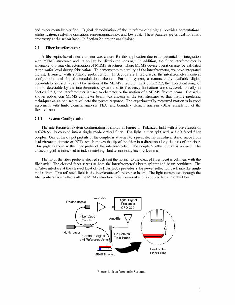
and experimentally verified. Digital demodulation of the interferometric signal provides computational sophistication, real-time operation, reprogrammability, and low cost. These features are critical for smart processing at the sensor head. In Section 2.4 are the conclusions. 2.2 Fiber Interferometer
A fiber-optic-based interferometer was chosen for this application due to its potential for integration
with MEMS structures and its ability for distributed sensing. In addition, the fiber interferometer is amenable to in situ characterization of MEMS structures, where MEMS device operation may be validated at the wafer level during fabrication. To demonstrate this utility of the interferometer, we have integrated the interferometer with a MEMS probe station. In Section 2.2.1, we discuss the interferometer’s optical configuration and digital demodulation scheme. For this system, a commercially available digital demodulator is used to extract the motion of the MEMS structure. In Section 2.2.2, the theoretical range of motion detectable by the interferometric system and its frequency limitations are discussed. Finally in Section 2.2.3, the interferometer is used to characterize the motion of a MEMS flexure beam. The well-known polysilicon MEMS cantilever beam was chosen as the test structure so that mature modeling techniques could be used to validate the system response. The experimentally measured motion is in good agreement with finite element analysis (FEA) and boundary element analysis (BEA) simulation of the flexure beam.
2.2.1 System Configuration
The interferometer system configuration is shown in Figure 1. Polarized light with a wavelength of
m 6328.0 µ is coupled into a single mode optical fiber. The light is then split with a 3-dB fused fiber coupler. One of the output pigtails of the coupler is attached to a piezoelectric transducer stack (made from lead zirconate titanate or PZT), which moves the tip of the fiber in a direction along the axis of the fiber. This pigtail serves as the fiber probe of the interferometer. The coupler’s other pigtail is unused. The unused pigtail is immersed in index matching fluid to minimize back reflections.
The tip of the fiber probe is cleaved such that the normal to the cleaved fiber facet is collinear with the
fiber axis. The cleaved facet serves as both the interferometer’s beam splitter and beam combiner. The air/fiber interface at the cleaved facet of the fiber probe provides a 4% power reflection back into the single mode fiber. This reflected field is the interferometer’s reference beam. The light transmitted through the fiber probe’s facet reflects off the MEMS structure to be measured and is coupled back into the fiber.
Digital SignalProcessorOPD-200
Photodetector
PZT-drivenFiber Probe
MEMS Structure
Fiber OpticCoupler
HeNe LaserCommon Signal
and Reference Arms
Amplifier
Amplifier
Inset of the Fiber Probe
'∆
Figure 1. Interferometric System.
3

(a)
Single ModeFiber
MEMS Cantilevered Beam
Probe/TargetSeparation
0 100 200 300 4000
20
40
60
80
100
Probe/Target Separation Distance (µm)
Pow
er C
oupl
ing
Effic
ienc
y (%
)
(b)
Single ModeFiber
MEMS Cantilevered Beam
100 µm
-10 -8 -6 -4 -2 0 2 4 6 8 100
2
4
6
8
10
12
14
Tilt Angle (degrees)
Pow
er C
oupl
ing
Effic
ienc
y (%
)
(a)
(b)
Figure 2. Analysis of the power coupling efficiency Figure 3. Analysis of the power coupling efficiency of the fiber probe: (a) geometry of the system and of the fiber probe: (a) geometry of the system and (b) power coupling efficiency versus probe/target (b) power coupling efficiency versus tilt angle of the separation distance at zero degree tilt of the fiber axis fiber axis with respect to the target normal at a with respect to the target normal. separation distance of 100 µm.
Consequently, the cleaved facet now acts as a beam combiner. The round trip distance traveled out of the fiber, off the MEMS structure, and back into the fiber forms the signal path of the interferometer. The reference and signal fields co-propagate back through the fiber until they reach the fused fiber coupler, where an additional 3-dB power reduction is encountered. Finally, the interference signal is detected with a photodetector.
The coupling efficiency of the signal field back into the fiber probe is a critical feature of this
interferometer configuration. We have modeled the coupling efficiency of the fiber probe, assuming Gaussian field propagation out of the fiber and reflection off a tilted specular surface. The power coupling efficiency versus the probe-to-target separation distance is plotted in Figure 2. Given zero tilt of the fiber probe with respect to the target surface normal, the probe-to-target separation distance must be less than
m 195 µ for greater than 4% power coupling of the signal field back into the fiber. Figure 3 shows the power coupling efficiency versus probe tilt angle at a separation distance of
m 100 µ . From an implementation perspective, high tolerance to angular misalignment of the probe is
desired. The bare fiber probe tolerates approximately of misalignment at a separation distance of o4±m 100 µ . This limitation is sufficient for the in situ characterization of MEMS structures.
The optical configuration described above has been used with varying demodulation schemes to
characterize MEMS sensors [15], hard disk surfaces [25], and biological membranes [26]. The common signal and reference paths in this optical configuration eliminate signal fading due to non-signal induced polarization drift and optical path length drift in the fiber. Also, the common signal and reference paths obviate the need for high-cost polarization-preserving single mode fiber.
4
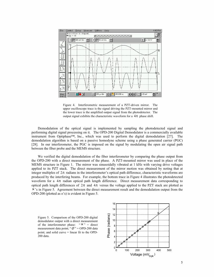
Figure 4. Interferometric measurement of a PZT-driven mirror. The upper oscilloscope trace is the signal driving the PZT-mounted mirror and the lower trace is the amplified output signal from the photodetector. The output signal exhibits the characteristic waveform for a π4 phase shift.
Demodulation of the optical signal is implemented by sampling the photodetected signal and
performing digital signal processing on it. The OPD-200 Digital Demodulator is a commercially available instrument from Optiphase™, Inc., which was used to perform the digital demodulation [27]. The demodulation algorithm is based on a passive homodyne scheme using a phase generated carrier (PGC) [28]. In our interferometer, the PGC is imposed on the signal by modulating the open air signal path between the fiber probe and the MEMS structure.
We verified the digital demodulation of the fiber interferometer by comparing the phase output from
the OPD-200 with a direct measurement of the phase. A PZT-mounted mirror was used in place of the MEMS structure in Figure 1. The mirror was sinusoidally vibrated at 1 kHz with varying drive voltages applied to its PZT stack. The direct measurement of the mirror motion was obtained by noting that at integer multiples of π2 radians in the interferometer’s optical path difference, characteristic waveforms are produced by the interfering beams. For example, the bottom trace in Figure 4 illustrates the photodetected waveform for a π4 radian optical path length difference. Direct measurement data corresponding to optical path length differences of π2 and π4 versus the voltage applied to the PZT stack are plotted as
’s in Figure 5. Agreement between the direct measurement result and the demodulation output from the OPD-200 (plotted as o’s) is evident in Figure 5. ×
Voltage (mV0-pk )0 100 200 300 400 500
0
2
4
6
8
10
12
14
16
Phas
e (ra
dian
s)
Figure 5. Comparison of the OPD-200 digital demodulator output with a direct measurement of the interferometer phase: “ ” = direct measurement data point; “
×ο ” = OPD-200 data
point; and solid curve = linear fit to the OPD-200 data.
5

2.2.2 System Dynamic Range The displacement measurement and frequency response of the interferometer system described above
has a large dynamic range. The digital demodulation technique facilitates both fractional fringe and fringe counting interrogation of the interferometric signal. This technique has a theoretical dynamic range greater than 10 for measuring surface displacements. 8
The ultimate system resolution of a displacement measuring interferometer refers to a limit in the
system’s ability to detect surface changes. This limit is expressed in terms of the smallest displacement that can be detected if the signal-to-noise ratio (SNR) is unity [29]. Photodetector quantum noise and analog-to-digital converter quantization noise are examples of noise sources that cannot be eliminated from the system. In the present system, the detector quantum noise (also called shot noise) sets the limit to the ultimate performance of the interferometric system. We have determined the quantum-noise-limited sensitivity of the interferometer shown in Figure 1 to be 24 pm. The derivation of the ultimate system resolution for the classical Michelson interferometer is given in Appendix A.
The degree to which this ultimate resolution may be achieved depends on numerous factors. The
foremost consideration for this interferometer configuration is the field contrast ratio. In practice, it is very difficult to secure a unity field contrast ratio. For values of field contrast not equal to one, the fringe contrast and the SNR decrease, thereby increasing the minimum detectable displacement. In practice, we have achieved a system resolution of several nanometers.
The number of bits in the digital demodulator, which are used to keep the fringe count, limits the full
measurement range of the interferometer. This limitation places an upper bound of 2.6 mm on the measurement range. The practical measurement range of several nanometers to more than two and a half millimeters is well-suited to the out-of-plane characterization of MEMS structures.
The interferometric system is capable of measuring displacements ranging in frequency from dc to
one-half the frequency of the phase generated carrier. The OPD-200 provides the drive signal for the phase generated carrier and is capable of modulation rates up to 95 kHz. In our interferometric configuration, however, the PZT stack limits the modulation frequency. The PZT and drive electronics in our system limit the carrier frequency to 10 kHz. Therefore, our system is capable of measuring displacements ranging from dc to 5 kHz. 2.2.3 Characterization of a MEMS Flexure Beam
A MEMS flexure beam is a clamped-free cantilever beam, where a small section of the beam material
near the base of the post has been removed to produce a hinge point on the beam (see Figure 6). Polysilicon flexure beams with dimensions given in Figure 6 were fabricated via the Multi-User MEMS Processes (MUMPs®) foundry service available from JDS Uniphase [30]. We used the fiber
(a)
(b)
3.5-µm-thickpolysilicon post
2-µm-thickflexurearms
200 µm
50 µm
2-µm-thicksacrificial oxide
bottomelectrode
3.5-µm-thickpolysilicon beam
xy
z
x
Figure 6. Geometry of a MEMS flexure beam: (a) top view and (b) side view.
6
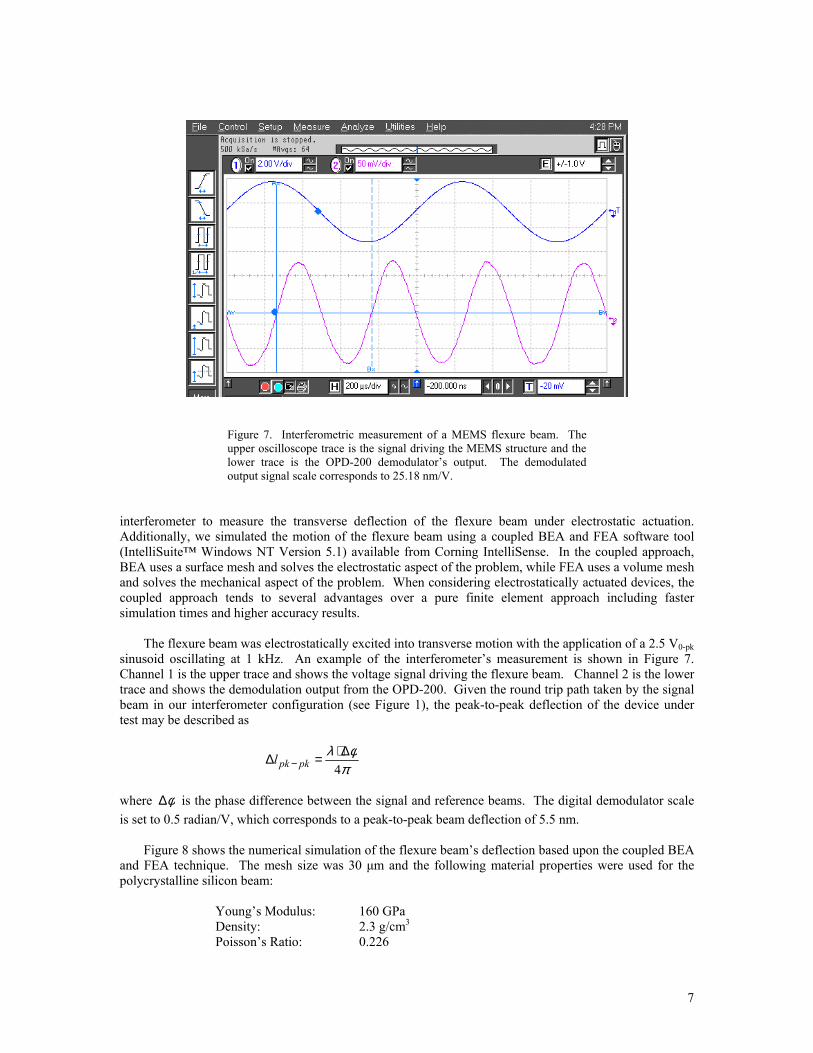
Figure 7. Interferometric measurement of a MEMS flexure beam. The upper oscilloscope trace is the signal driving the MEMS structure and the lower trace is the OPD-200 demodulator’s output. The demodulated output signal scale corresponds to 25.18 nm/V.
interferometer to measure the transverse deflection of the flexure beam under electrostatic actuation. Additionally, we simulated the motion of the flexure beam using a coupled BEA and FEA software tool (IntelliSuite™ Windows NT Version 5.1) available from Corning IntelliSense. In the coupled approach, BEA uses a surface mesh and solves the electrostatic aspect of the problem, while FEA uses a volume mesh and solves the mechanical aspect of the problem. When considering electrostatically actuated devices, the coupled approach tends to several advantages over a pure finite element approach including faster simulation times and higher accuracy results.
The flexure beam was electrostatically excited into transverse motion with the application of a 2.5 V0-pk
sinusoid oscillating at 1 kHz. An example of the interferometer’s measurement is shown in Figure 7. Channel 1 is the upper trace and shows the voltage signal driving the flexure beam. Channel 2 is the lower trace and shows the demodulation output from the OPD-200. Given the round trip path taken by the signal beam in our interferometer configuration (see Figure 1), the peak-to-peak deflection of the device under test may be described as
π
φλ4∆⋅=∆ − pkpkl
where φ∆ is the phase difference between the signal and reference beams. The digital demodulator scale is set to 0.5 radian/V, which corresponds to a peak-to-peak beam deflection of 5.5 nm.
Figure 8 shows the numerical simulation of the flexure beam’s deflection based upon the coupled BEA
and FEA technique. The mesh size was 30 µm and the following material properties were used for the polycrystalline silicon beam:
Young’s Modulus: 160 GPa Density: 2.3 g/cm3
Poisson’s Ratio: 0.226
7

Figure 8. Coupled boundary element analysis and finite element analysis simulation of a MEMS flexure beam. The signal driving the MEMS beam is )10002sin(5.2 t⋅π V.
The data in Figure 8 indicates that the flexure beam deflects toward the substrate with a frequency of 2 kHz and a peak-to-peak amplitude of 4.0 nm. This simulation result compares favorably with the experimental data.
Of particular interest is the oscillation frequency of the flexure beam. The demodulation output shown
in the lower trace of Figure 7 indicates that the flexure beam is oscillating at 2 kHz or twice the excitation frequency. During the negative voltage portion of the excitation sinusoid’s period (see Figure 9a), the E
r
field is directed in the -direction. The negative charge, , accumulated on the beam’s electrode
experiences a force given by
)( z+ Q−
EQFrr
−= ; so, the beam is deflected towards the substrate. During the
positive voltage portion of the excitation sinusoid’s period (see Figure 9b), the Er
field is directed in the -direction. The positive charge, Q , accumulated on the beam’s electrode experiences a force )( z−
QF Err
= ; so, the beam is again deflected towards the substrate. Electrostatically driven MEMS structures experience only electrostatic attraction (as opposed to
electrostatic repulsion). Thus, for a bipolar excitation signal with zero mean, the oscillation frequency of the beam is twice that of the excitation signal. This frequency doubling effect may be removed by adding a dc bias to the excitation signal such that the excitation signal is always a positive voltage or always a negative voltage. Figure 10 shows a biased excitation signal (upper trace) and the raw interferometer output signal prior to digital demodulation (lower trace). The excitation signal is )10002sin(55 t⋅+ π V. Note that both the excitation and the raw interferometer’s response are oscillating at 1 kHz.
Two points of clarification are necessary with respect to the interferometer data displayed in Figure 7.
First, the interferometer measures relative phase shifts between a reference light wave and a signal light wave. The demodulator reads both the offset phase (comprising the optical path mismatch) as well as the dynamic signal created by the beam flexure. Therefore, a zero voltage reading at the demodulator output
8

V+
V
+
(a)
(b)
Er
Er
z
x
- - - - - - -
+++++++
Figure 9. Electrostatic attraction of a MEMS cantilever beam: (a) negative voltage applied to the beam and (b) positive voltage applied to the beam.
Figure 10. Removal of the frequency doubling effect. The upper oscilloscope trace is a biased excitation signal driving the MEMS structure and the lower trace is the raw interferometer output signal prior to demodulation. The signal driving the MEMS beam is 5 )10002sin(5 t⋅+ π V.
9

does not necessarily correspond to zero deflection. Second, an artifact of the digital demodulation scheme is a fixed time delay in the output data, which corresponds to the time for one demodulation cycle. For the modulation frequency used in Figure 7, the delay is about 1 s 24 µ .
Finally, we measured the deflection at the tip of the flexure beam as a function of the excitation
voltage at 1 kHz. As shown in Figure 11, the experimentally measured data is in reasonably good agreement with the simulation data. However, a discrepancy in deflection amplitudes at the larger excitation voltages exists between the experimental and the simulation data. Further simulation results indicate that magnitude of this discrepancy is not attributable to practical variations in the beam parameters (e.g., Young’s modulus and beam length) or to the onset of spontaneous collapse of the flexure beam. Furthermore, simulation indicates that the flexure beam has a transverse mode resonance at 73 kHz. Our beam oscillation frequency of 2 kHz is sufficiently removed from resonance such that overshoot of the beam cannot be the cause of the discrepancy. This discrepancy between the experiment and simulation is currently under investigation.
0 2 4 6 8 100
20
40
60
80
100
120
140
Applied Voltage (V0-pk)
Tip
Def
lect
ion
(nm
pk-p
k)
Figure 11. Tip deflection of the MEMS flexure beam versus applied voltage at a frequency of 1 kHz: “ ” = FEA simulation data point; solid curve = quadratic curve fit to the simulation data; “
×
ο ” = experimental data point; and dotted curve = quadratic curve fit to the experimental data.
10
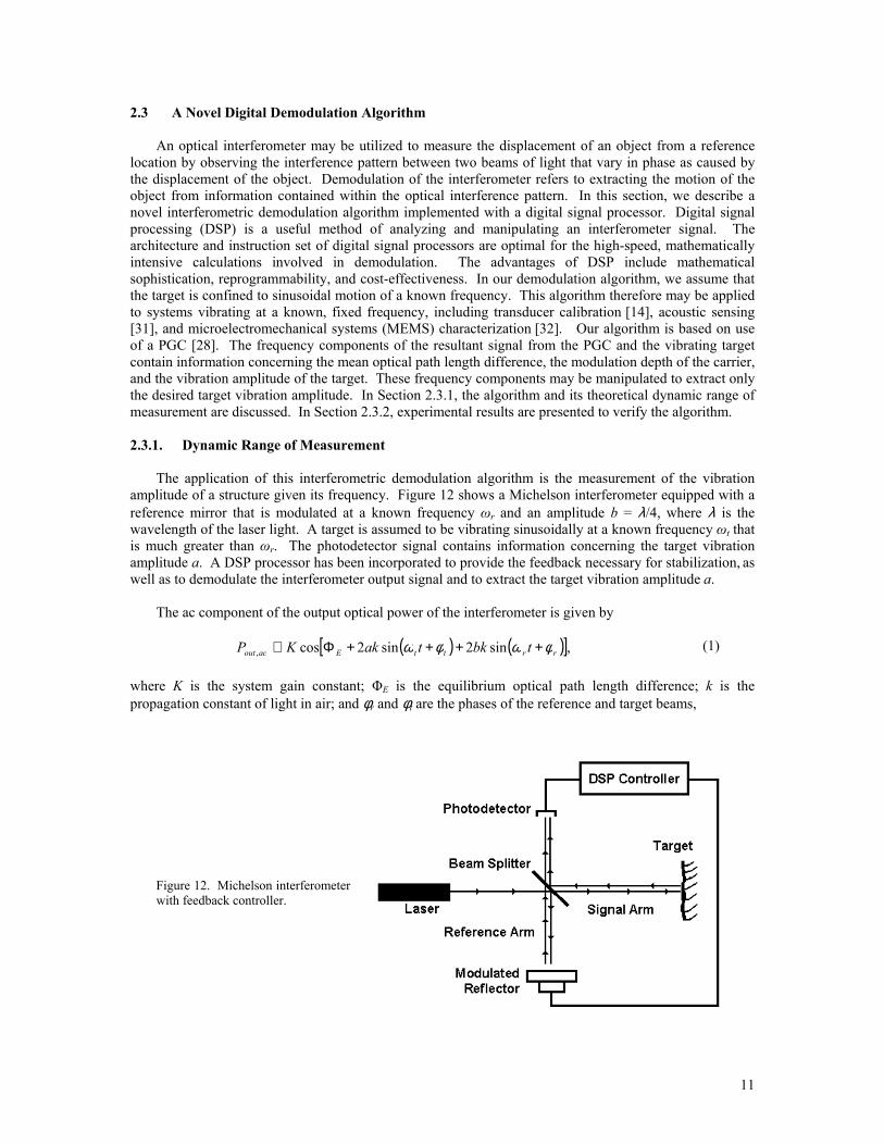
2.3 A Novel Digital Demodulation Algorithm
An optical interferometer may be utilized to measure the displacement of an object from a reference location by observing the interference pattern between two beams of light that vary in phase as caused by the displacement of the object. Demodulation of the interferometer refers to extracting the motion of the object from information contained within the optical interference pattern. In this section, we describe a novel interferometric demodulation algorithm implemented with a digital signal processor. Digital signal processing (DSP) is a useful method of analyzing and manipulating an interferometer signal. The architecture and instruction set of digital signal processors are optimal for the high-speed, mathematically intensive calculations involved in demodulation. The advantages of DSP include mathematical sophistication, reprogrammability, and cost-effectiveness. In our demodulation algorithm, we assume that the target is confined to sinusoidal motion of a known frequency. This algorithm therefore may be applied to systems vibrating at a known, fixed frequency, including transducer calibration [14], acoustic sensing
[31], and microelectromechanical systems (MEMS) characterization [32]. Our algorithm is based on use of a PGC [28]. The frequency components of the resultant signal from the PGC and the vibrating target contain information concerning the mean optical path length difference, the modulation depth of the carrier, and the vibration amplitude of the target. These frequency components may be manipulated to extract only the desired target vibration amplitude. In Section 2.3.1, the algorithm and its theoretical dynamic range of measurement are discussed. In Section 2.3.2, experimental results are presented to verify the algorithm. 2.3.1. Dynamic Range of Measurement
The application of this interferometric demodulation algorithm is the measurement of the vibration amplitude of a structure given its frequency. Figure 12 shows a Michelson interferometer equipped with a reference mirror that is modulated at a known frequency ωr and an amplitude b = λ/4, where λ is the wavelength of the laser light. A target is assumed to be vibrating sinusoidally at a known frequency ωt that is much greater than ωr. The photodetector signal contains information concerning the target vibration amplitude a. A DSP processor has been incorporated to provide the feedback necessary for stabilization, as well as to demodulate the interferometer output signal and to extract the target vibration amplitude a.
The ac component of the output optical power of the interferometer is given by
( ) ([ ],sin2sin2cos, rrttEacout tbktakKP )φωφω ++++Φ∝ (1)
where K is the system gain constant; ΦE is the equilibrium optical path length difference; k is the propagation constant of light in air; and φr and φt are the phases of the reference and target beams,
Figure 12. Michelson interferometer with feedback controller.
11
Photodetector r -,
Beam Splitter
—■ ■ Laser
DSP Controller
Target
^ > >
Signal Arm / s
Reference Arm
Modulated | | Reflector L_l

respectively. As the target vibration amplitude increases, the interferometer output signal exhibits higher-order harmonics. By applying the Fourier-Bessel expansion [33] to Equation (1), the harmonic content of this signal is revealed:
(2)
( ) ( ) ( ){( ) ( ) ( ) ( )( ) ( ) ( ) ( )( ) ( ) ( ) ( )( ) ( ) ( ) ( )( ) ( ) ( ) ( )( ) ( ) ( ) ( )( ) ( ) ( ) ( )( ) ( ) ( ) ( )( ) ( ) ( ) ( ) },22sin22sin2
22sin22sin222sin22cos2
cos22cos2cos22cos2sin22sin2
33sin22sin222sin22cos2
sin22sin222cos
12
12
02
11
11
01
30
20
10
00,
KrtrtE
rtrtE
ttE
rtrtE
rtrtE
ttE
rrE
rrE
rrE
Eacout
ttbkJakJttbkJakJ
tbkJakJttbkJakJ
ttbkJakJtbkJakJ
tbkJakJtbkJakJ
tbkJakJbkJakJKP
φφωωφφωω
φωφφωω
φφωωφω
φωφω
φω
+−+−Φ−+++Φ−
+Φ++−+−Φ−
+++Φ−+Φ−
+Φ−+Φ+
+Φ−Φ∝
where Jn(•) is an nth order Bessel function of the first kind. Note that many of the harmonics contain identical factors in their amplitudes. Two carefully selected frequency components may be detected and manipulated for demodulation. These signal components are expressed as
( ) ( ) ( ) ( ) ( )rrEC tbkJakJKaX φω +Φ−= sin22sin2* 10 and ( ) ( ) ( ) ( ) ( )rtrtED ttbkJakJKaX φφωω +++Φ−= 22sin22sin2* 12 . (3)
The angular frequencies of XC and XD are ωr and 2ωt + ωr, respectively. These specific terms have
been chosen such that sin(ΦE), J1(2bk), and K are strategically removed by taking the ratio of their amplitudes. This reveals a measurable quantity that is only a function of the desired target vibration amplitude a, given by the equation
( )( )
( )( )akJ
akJaXaX
D
C
22
2
0= . (4)
This is significant in that it allows demodulation to be completely independent of the equilibrium optical path length difference ΦE, the modulation depth 2bk, and the system gain K. By implementing a root-finding algorithm, such as bracketing and bisection [34], the argument 2ak of Equation (4) may be extracted. Further division by 2k reveals the target vibration amplitude, a.
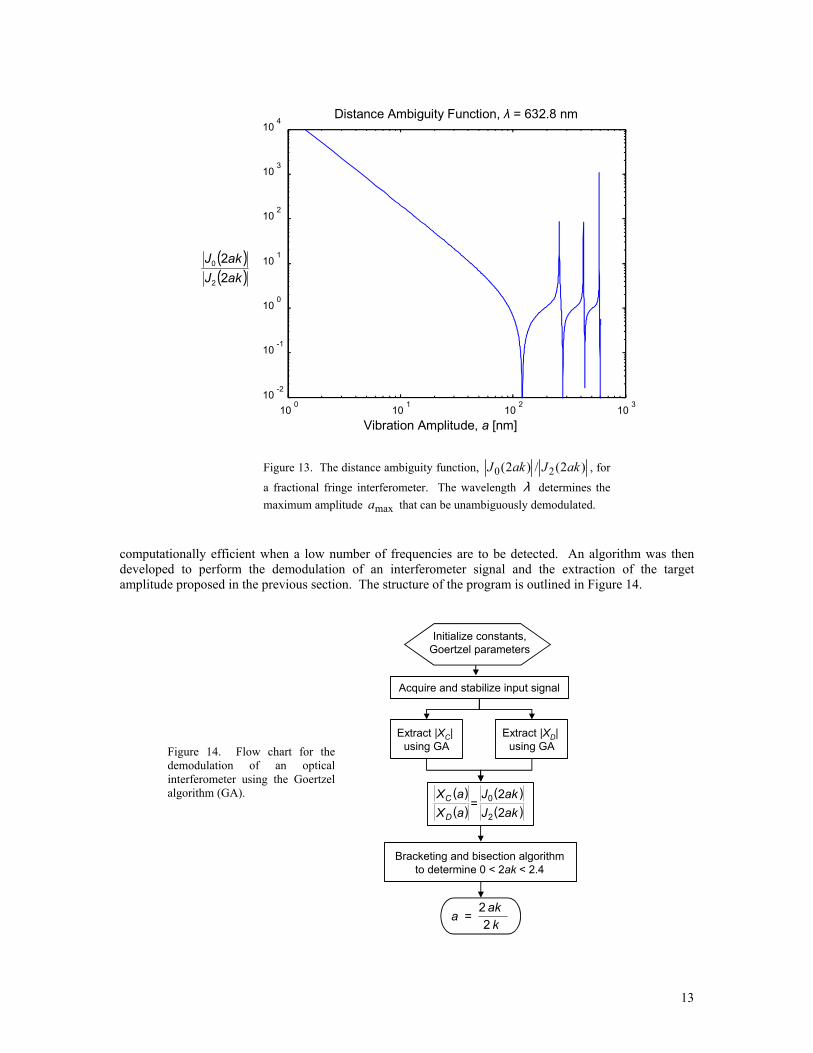
Figure 13 plots Equation (4) versus amplitude a, indicating a maximum detectable amplitude. Because
the demodulation scheme involves measuring the value of a function that has reoccurring poles and zeros with increasing values of a, amplitude certainty can only be guaranteed below the first zero of |J0(2ak)|/|J2(2ak)|. This is known as the distance ambiguity function. For an operating wavelength λ = 632.8 nm, amax ≈ 120 nm. The minimum detectable displacement due to quantum shot noise for this phase-generated carrier demodulation scheme is amin = 5 pm (see Appendix A). Therefore, the measurement dynamic range of this system is on the order of 105.
2.3.2. Experimental Verification
The TMS320C31 32-bit floating-point digital signal processor, provided with the Digital Signal
Processor Starter’s Kit (DSK) available from Texas Instruments, Inc., was used to stabilize the interferometer’s operating point at quadrature and to demodulate the interferometer output signal. The TMS320C31 DSK was programmed using the digital stabilization scheme based on the Goertzel algorithm (GA) developed by our group [35]. The Goertzel algorithm is a filtering adaptation of the discrete Fourier transform (DFT). Compared to the fast Fourier transform (FFT), the Goertzel algorithm is
12
( )( )akJakJ
22
2
0
10 10 10 100 1 2 310
10
10
10
10
10
10
-2
-1
0
1
2
3
4Distance Ambiguity Function, λ = 632.8 nm
Vibration Amplitude, a [nm]
Figure 13. The distance ambiguity function, )2(/)2( 20 akJakJ , for
a fractional fringe interferometer. The wavelength λ determines the maximum amplitude that can be unambiguously demodulated. maxa
computationally efficient when a low number of frequencies are to be detected. An algorithm was then developed to perform the demodulation of an interferometer signal and the extraction of the target amplitude proposed in the previous section. The structure of the program is outlined in Figure 14.
Figure 14. Flow chart for the demodulation of an optical interferometer using the Goertzel algorithm (GA).
Initialize constants, Goertzel parameters
Acquire and stabilize input signal
Extract |XC| using GA
Bracketing and bisection algorithmto determine 0 < 2ak < 2.4
kak
a 22
=
Extract |XD| using GA
( )( )
( )( )akJakJ
=aXaX
D
C
22
2
0
13

A test of the demodulation process involved creating a signal that sufficiently represented the interferometer output by simulating only those frequency components necessary for demodulation. Since Equation (2) indicates that the interferometer output signal is composed of a sum of harmonics, a simulation of the interferometer output signal was synthesized by summing a pair of sinusoids. Recalling Equation (4), the simulated target vibration amplitude a was varied by adjusting the ratio of the sinusoid amplitudes.
The demodulation parameters were set for a reference frequency of fr = 315 Hz and a target frequency
ft = 2008 Hz. Therefore, the frequencies to be detected were fC = 315 Hz and fD = 4331 Hz. A multifunction synthesizer was used to create the simulated interferometer signal
( ) ( ) ( )tXtXtv DC ⋅⋅+⋅⋅= 43312sin3152sin ππ [V]. (5)
A set of simulated signals was defined according to the parameters listed in Table 1. The range of the
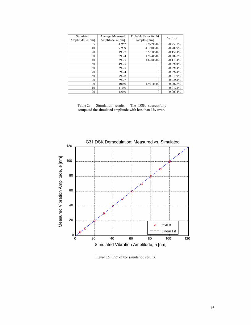
analog-to-digital converter (ADC) of the DSK was limited to ±1.5 V. The magnitudes of XC and XD were selected such that their sum did not exceed 1.5 V. Table 2 and Figure 15 show that the DSK successfully demodulated the simulated interferometer output signal precisely to within 0.1 nm and accurately to within 1% of the simulated value.
The next objective was to test the stabilization/demodulation routine on an appropriate system that is
easily characterized. To accomplish this task, a PZT stack was chosen to be the vibrating target. The optical interferometer configuration is described in Section 2.2.1 and shown in Figure 1.
The distance through which a vibrating object oscillates may be estimated by observing the
interference pattern created in the interferometer output signal. Peak-to-peak phase shifts at multiples of 2π display characteristic waveforms that are easily identifiable when viewed with an oscilloscope. When operating at quadrature, these waveforms are symmetric about their average as illustrated in Figure 16. According to this phenomenon, the PZT was characterized by a direct measurement of phase. The voltages corresponding to the target PZT zero-to-peak phase shifts 2ak = {π, 2π, 3π} were recorded. The phase shifts were converted to amplitudes through the relationship
=
422 λ
πaka . (6)
Simulated Amplitude, a [nm]
( )( )
( )( )akJ
akJaXaX
D
C22
2
0= |XC| [MV] |XD| [MV]
5 810.11926 1000 1.234 10 201.52956 1000 4.962 20 49.38136 1000 20.25 30 21.20452 1000 47.16 40 11.34114 1000 88.17 50 6.77411 1000 147.6 60 4.29140 1000 233.0 70 2.79238 1000 358.1 80 1.81725 500 275.1 90 1.14629 500 436.2
100 0.66371 500 753.3 110 0.30370 303.7 1000 120 0.02657 26.57 1000
Table 1. The values |XC| and |XD| used to simulate an interferometer signal corresponding to various target amplitudes a.
14
Simulated
Amplitude, a [nm] Average Measured Amplitude, a [nm]
Probable Error for 24 samples [nm] % Error
5 4.952 8.972E-02 -0.9573% 10 9.909 4.360E-02 -0.9097% 20 19.97 2.533E-02 -0.1514% 30 29.94 1.994E-02 -0.2022% 40 39.95 1.628E-02 -0.1174% 50 49.95 0 -0.0901% 60 59.95 0 -0.0914% 70 69.94 0 -0.0924% 80 79.98 0 -0.0197% 90 89.97 0 -0.0284%
100 100.0 1.941E-02 0.0028% 110 110.0 0 0.0124% 120 120.0 0 0.0031%
Table 2: Simulation results. The DSK successfully computed the simulated amplitude with less than 1% error.
0 20 40 60 80 100 1200
20
40
60
80
100
120C31 DSK Demodulation: Measured vs. Simulated
Mea
sure
d Vi
brat
ion
Ampl
itude
, a[n
m]
Simulated Vibration Amplitude, a [nm]
a vs a
Linear Fit
Figure 15. Plot of the simulation results.
15

2ak = π 2ak = 2π
2ak = 3π
Time
Sign
al L
evel
2ak = 4π
Characteristic Phase Waveforms
Figure 16. Characteristic waveforms at the output of an interferometer stabilized at quadrature. The reference arm is static and the target is vibrating at an amplitude 2ak.
These known amplitudes are plotted versus their respective driving voltages in Figure 17. A linear fit
to this data reveals a non-zero a when 0 V is applied. Therefore, the voltage-amplitude relationship for the PZT was created in a piece-wise linear fashion such that
( ) ( )
≥−≤
=
=
ππλ
π akVakVVakVa
2,1094.128370.02,7812.0
422 (7)
where a is in units of [nm] and V is in units of [mV].
PZT Linearity @ ft = 2008 Hz
Drive Voltage, V [mV0-pk]
Ampl
itude
, a(V
) = 0
.837
0V-1
2.10
94 [n
m]
0 100 200 300 400 500 600 700 800-100
0
100
200
300
400
500
600
700
a vs V
Linear Fit
Figure 17. Linear approximation of the V0 characteristic of
a vibrating PZT stack.
apk −−
16
0 50 100 150 200 250 300 350 400 450
Bessel Plot: Experimental and Theoretical
Vibration Amplitude, a [nm]
Probable Error: 24 samplesExperimental MeanTheory
( )( )akJakJ
22
2
0
10
10
10
10
10
10
10
-2
-1
0
1
2
3
4
Figure 18. Plot of the theoretical )2(/)2( 20 akJakJ and the
experimental )(/)( aXaX DC as a function of . a
Equation (7) was then used to test the ability of the DSK to compute the demodulation amplitude a
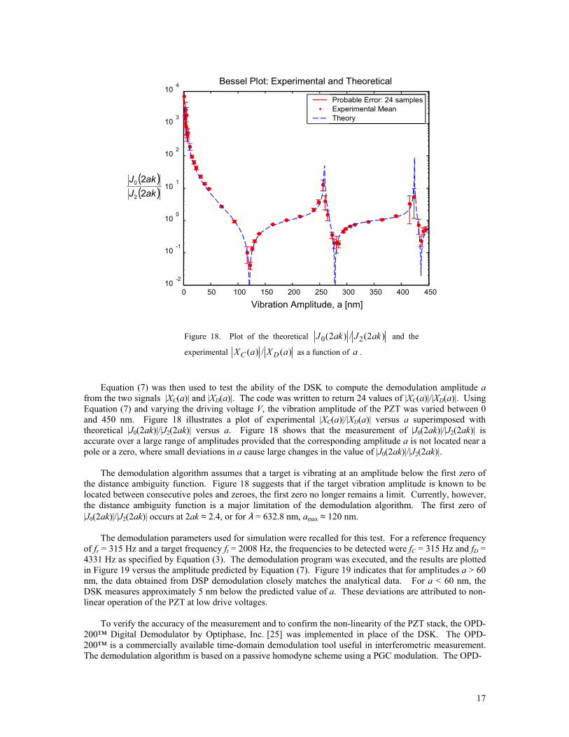
from the two signals |XC(a)| and |XD(a)|. The code was written to return 24 values of |XC(a)|/|XD(a)|. Using Equation (7) and varying the driving voltage V, the vibration amplitude of the PZT was varied between 0 and 450 nm. Figure 18 illustrates a plot of experimental |XC(a)|/|XD(a)| versus a superimposed with theoretical |J0(2ak)|/|J2(2ak)| versus a. Figure 18 shows that the measurement of |J0(2ak)|/|J2(2ak)| is accurate over a large range of amplitudes provided that the corresponding amplitude a is not located near a pole or a zero, where small deviations in a cause large changes in the value of |J0(2ak)|/|J2(2ak)|.
The demodulation algorithm assumes that a target is vibrating at an amplitude below the first zero of
the distance ambiguity function. Figure 18 suggests that if the target vibration amplitude is known to be located between consecutive poles and zeroes, the first zero no longer remains a limit. Currently, however, the distance ambiguity function is a major limitation of the demodulation algorithm. The first zero of |J0(2ak)|/|J2(2ak)| occurs at 2ak ≈ 2.4, or for λ = 632.8 nm, amax ≈ 120 nm.
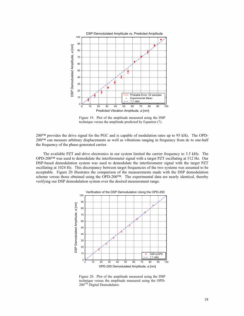
The demodulation parameters used for simulation were recalled for this test. For a reference frequency
of fr = 315 Hz and a target frequency ft = 2008 Hz, the frequencies to be detected were fC = 315 Hz and fD = 4331 Hz as specified by Equation (3). The demodulation program was executed, and the results are plotted in Figure 19 versus the amplitude predicted by Equation (7). Figure 19 indicates that for amplitudes a > 60 nm, the data obtained from DSP demodulation closely matches the analytical data. For a < 60 nm, the DSK measures approximately 5 nm below the predicted value of a. These deviations are attributed to non-linear operation of the PZT at low drive voltages.
To verify the accuracy of the measurement and to confirm the non-linearity of the PZT stack, the OPD-
200™ Digital Demodulator by Optiphase, Inc. [25] was implemented in place of the DSK. The OPD-200™ is a commercially available time-domain demodulation tool useful in interferometric measurement. The demodulation algorithm is based on a passive homodyne scheme using a PGC modulation. The OPD-
17
0 10 20 30 40 50 60 70 80 90 1000
10
20
30
40
50
60
70
80
90
100DSP-Demodulated Amplitude vs. Predicted Amplitude
DSP
Dem
odul
ated
Am
plitu
de, a
[nm
]
Predicted Vibration Amplitude, a [nm]
Probable Error: 24 samplesExperimental Mean1:1 ratio
Figure 19. Plot of the amplitude measured using the DSP technique versus the amplitude predicted by Equation (7).
200™ provides the drive signal for the PGC and is capable of modulation rates up to 95 kHz. The OPD-200™ can measure arbitrary displacements as well as vibrations ranging in frequency from dc to one-half the frequency of the phase-generated carrier.
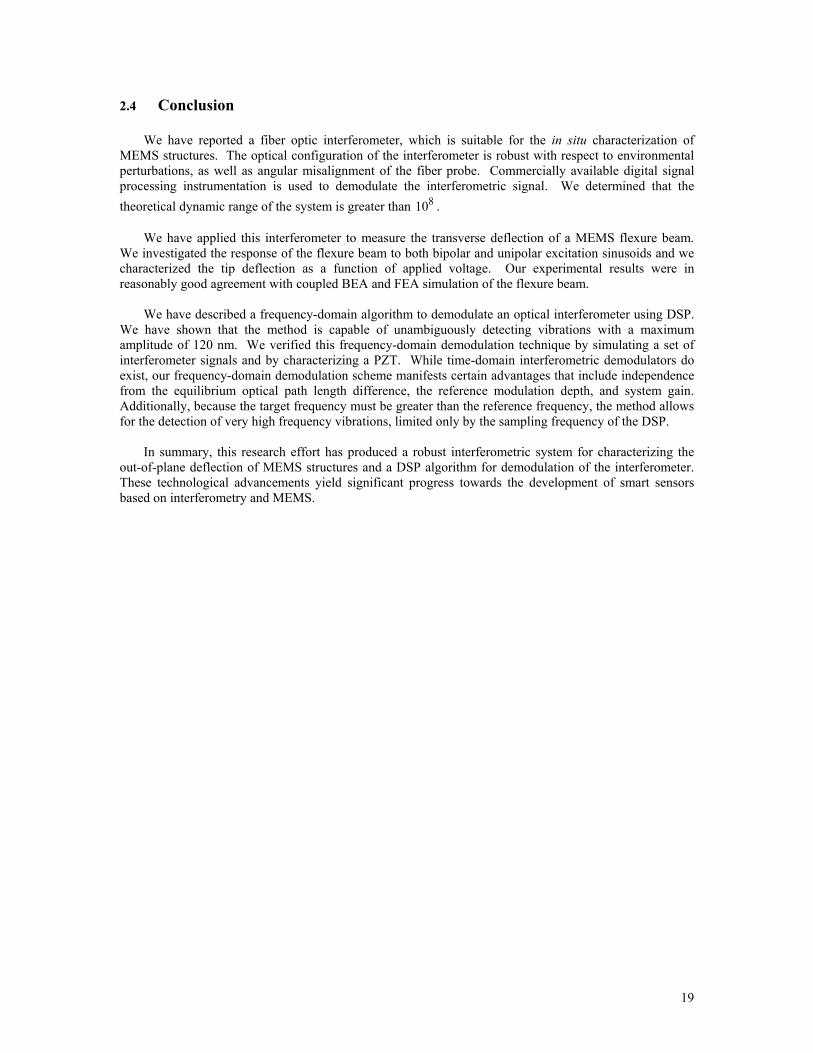
The available PZT and drive electronics in our system limited the carrier frequency to 3.5 kHz. The
OPD-200™ was used to demodulate the interferometer signal with a target PZT oscillating at 512 Hz. Our DSP-based demodulation system was used to demodulate the interferometer signal with the target PZT oscillating at 1024 Hz. This discrepancy between target frequencies of the two systems was assumed to be acceptable. Figure 20 illustrates the comparison of the measurements made with the DSP demodulation scheme versus those obtained using the OPD-200™. The experimental data are nearly identical, thereby verifying our DSP demodulation system over the desired measurement range.
0 10 20 30 40 50 60 70 80 90 1000
10
20
30
40
50
60
70
80
90
100Verification of the DSP Demodulation Using the OPD-200
OPD-200 Demodulated Amplitude, a [nm]
DSPvsOPD1:1 ratio
DSP
Dem
odul
ated
Am
plitu
de, a
[nm
]
Figure 20. Plot of the amplitude measured using the DSP technique versus the amplitude measured using the OPD-200TM Digital Demodulator.
18
2.4 Conclusion
We have reported a fiber optic interferometer, which is suitable for the in situ characterization of MEMS structures. The optical configuration of the interferometer is robust with respect to environmental perturbations, as well as angular misalignment of the fiber probe. Commercially available digital signal processing instrumentation is used to demodulate the interferometric signal. We determined that the theoretical dynamic range of the system is greater than 10 . 8
We have applied this interferometer to measure the transverse deflection of a MEMS flexure beam.
We investigated the response of the flexure beam to both bipolar and unipolar excitation sinusoids and we characterized the tip deflection as a function of applied voltage. Our experimental results were in reasonably good agreement with coupled BEA and FEA simulation of the flexure beam.
We have described a frequency-domain algorithm to demodulate an optical interferometer using DSP.
We have shown that the method is capable of unambiguously detecting vibrations with a maximum amplitude of 120 nm. We verified this frequency-domain demodulation technique by simulating a set of interferometer signals and by characterizing a PZT. While time-domain interferometric demodulators do exist, our frequency-domain demodulation scheme manifests certain advantages that include independence from the equilibrium optical path length difference, the reference modulation depth, and system gain. Additionally, because the target frequency must be greater than the reference frequency, the method allows for the detection of very high frequency vibrations, limited only by the sampling frequency of the DSP.
In summary, this research effort has produced a robust interferometric system for characterizing the out-of-plane deflection of MEMS structures and a DSP algorithm for demodulation of the interferometer. These technological advancements yield significant progress towards the development of smart sensors based on interferometry and MEMS.
19
3. Publications Supported Under this Contract 3.1 Peer-Reviewed Journals 1. T. J. Tayag, E. S. Kolesar, B. D. Pitt, K. S. Hoon, J. Marchetti, and I. H. Jafri, “An optical fiber
interferometer for measuring the in situ deflection characteristics of MEMS structures,” Opt. Engineer., vol. 42, no. 1, pp. 105-111 (January 2003).
2. T. J. Tayag, “Quantum-noise-limited sensitivity of an interferometer using a phase generated carrier demodulation scheme,” Opt. Eng. Lett., vol. 41, no. 2, pp. 276-277 (February 2002).
3.2 Non-Peer-Reviewed Journals and Conference Proceedings 1. B. D. Pitt, T. J. Tayag, and M. L. Nelson, “Digital demodulation of an interferometer for the
characterization of vibrating microstructures,” Proceedings of the SPIE: Advance Characterization Techniques for Optics, Semiconductors, and Nanotechnologies, vol. 5188, San Diego, CA (August 2003).
2. B. D. Pitt, T. J. Tayag, and M. L. Nelson, “An algorithm for the digital demodulation of an
interferometer,” Proceedings of the ASEE Gulf-Southwest Annual Conference, Arlington, TX (March 2003). Note: Awarded 2nd Place in the Student Paper Contest.
3. J. Kern, S. D. Dimitrijevisch, T. J. Tayag, B. D. Pitt, T. H. Summers, and C. G. Davis, “An optical
system to characterize the gross contractile response of a tissue-equivalent collagen matrix,” Proceedings of the SPIE: Optical Technologies to Solve Problems in Tissue Engineering, vol. 4961, San Jose, CA (January 2003).
5. T. J. Tayag and C. A. Belk, “The application of digital signal processing to stabilize an interferometer
at quadrature,” Proceedings of the 10th International Conference on Electronics, Communications, and Computers: ConieleComp 2000, vol. 10, pp. 75-78 (February 2000).
6. C. A. Belk and T. J. Tayag, “Digital demodulation of a fractional fringe interferometer,” DSPS Fest ’99, www.ti.com/sc/dspsfest, Houston, TX (August 1999).
3.3 Presentations 1. T. J. Tayag “Interferometric sensing of MEMS and biological structures,” invited presentation, IEEE
MetroCON 2003, Arlington, TX (September 2003). 2. T. J. Tayag “Interferometric sensing of MEMS and biological structures,” invited presentation, The
Johns Hopkins University/Applied Physics Laboratory, Laurel, MD (July 2003). 3. B. D. Pitt, T. J. Tayag, E. S. Kolesar, W. E. Odom, and A. J. Jayachandran, “Integration of a fiber optic
interferometer with a MEMS probe station,” Metroplex Research Consortium for Electronic Devices and Materials (MRCEDM) Spring Poster Festival, Ft. Worth, TX (April 2003).
4. R. C. Watson and T. J. Tayag, “An algorithm for demodulating an interferometer in the frequency
domain,” Metroplex Research Consortium for Electronic Devices and Materials (MRCEDM) Spring Poster Festival, Ft. Worth, TX (April 2003).
20

5. B. K. Searcey, T. J. Tayag, B. D. Pitt, S. D. Dimitrijevisch, and J. Kern, “Development of an environmental chamber for the interferometric measurement of contracting fibroblast cells,” Metroplex Research Consortium for Electronic Devices and Materials (MRCEDM) Spring Poster Festival, Ft. Worth, TX (April 2003).
6. T. J. Tayag, S. D. Dimitrijevisch, J. Kern, T. H. Summers, and C. G. Davis, “Interferometric
measurement of contracting fibroblast cells within a collagen gel,” OSA Annual Meeting, Orlando, FL (October 2002).
7. T. J. Tayag, “Interferometric sensing of microelectromechanical system structures,” invited
presentation, Electro-Optics Department Seminar Series, University of Dayton, Dayton, OH (April 2002).
8. B. D. Pitt, T. J. Tayag, and E. S. Kolesar, “Simulation and optical characterization of MEMS
structures,” Metroplex Research Consortium for Electronic Devices and Materials (MRCEDM) Spring Poster Festival, Arlington, TX (April 2002).
9. T. H. Summers, C. G. Davis, T. J. Tayag, S. D. Dimitrijevisch, and J. Kern, “Development of an
interferometric system for measuring the contraction of biological cells,” Metroplex Research Consortium for Electronic Devices and Materials (MRCEDM) Spring Poster Festival, Arlington, TX (April 2002).
10. T. J. Tayag, E. N. Purdy, and E. S. Kolesar, “An optical sensor for the characterization of
microelectromechanical system structures,” invited presentation, IEEE MetroCON 2000, Arlington, TX (September 2000).
11. T. J. Tayag, “Research in integrated optics and digital signal processing at TCU,” Metroplex Research
Consortium for Electronic Devices and Materials (MRCEDM) Spring Poster Festival, Denton, TX (March 2000).
12. C. T. Moore and T. J. Tayag, “Interferometric characterization of microelectromechanical systems,” 5th
Annual Student Research Conf., West Texas A&M University, Canyon, TX (November 1998).
21

4. Scientific Personnel
During the course of this research program, the following undergraduate students participated as research assistants. Their degrees and anticipated or final graduation dates are listed.
• Brett K. Searcey, B.S. in Engineering and Biochemistry, TCU 2005
• Alisa N. Havens, transfer student
• Brandon D. Pitt, B. S. in Engineering , TCU 2004
• Tyler H. Summers, B.S. in Engineering, TCU 2004
• Casey G. Davis, B.S. in Engineering, TCU 2003
• Ezra N. Purdy, B. S in Engineering, TCU 2003
• R. Collins Watson, B.S. in Engineering, TCU 2003
• Mendy L. Nelson, B. S. in Engineering, TCU 2002
• Christopher A. Belk , B.S. in Engineering, TCU 2000
• Sunil K. Raju, transfer student
• Craig T. Moore, B. S. in Engineering, TCU 1999
22

5. List of Inventions 1. T. J. Tayag and C. A. Belk, “Method and system for stabilizing and demodulating an interferometer at
quadrature,” U. S. Patent (filed 2 February 2001).
23
6. Bibliography 1. D. T. Neilson and R. Ryf, “Scalable micro mechanical optical crossconnects,” Proc. LEOS 2000, vol.
1, pp. 48-49 (November 2000). 2. J. E. Ford, V. A. Aksyuk, D. J. Bishop, and J. A. Walker, “Wavelength add-drop switching using
tilting mirrors,” J. Lightwave Technol., vol. 17, no. 5, pp. 904-911 (May 1999). 3. J. E. Ford and J. A. Walker, “Dynamic spectral power equalization using micro-opto-mechanics,”
Photon. Technol. Lett., vol. 10, no. 10, pp.1440-1442 (October 1998). 4. C. J. Chang-Hasnain, “Tunable VSCEL,” J. Selected Topics in Quantum Electron., vol. 6, no. 6, pp.
978-981 (November/December 2000). 5. P. Tayebati, P. D. Wang, D. Vakhshoori, and R. N. Sacks, “Widely tunable Fabry-Perot filter using
Ga(Al)As-AlOx deformable mirrors,” Photon. Technol. Lett., vol. 10, no. 3, pp. 394-396 (March 1998). 6. C. Burrer, J. Esteve, and E. Lora-Tamayo, “Resonant silicon accelerometers in bulk micromachining
technology – An approach,” J. Microelectromech. Syst., vol. 5, no. 2, pp. 122-130 (June 1996). 7. H. Porte, V. Gorel, S. Kiryenko, J. P. Goedgebuer, W. Daniau, and P. Blind, “Imbalanced
Mach_Zehnder interferometer integrated in micromachined silicon substrate for pressure sensor,” J. Lightwave Technol., vol. 17, no. 2, pp. 229-233 (February 1999).
8. Z. Kadar, A. Bossche, and J. Mollinger, “Integrated resonant magnetic-field sensor,” Sensors and
Actuators A, vol. 41-42, pp. 66-69 (1994). 9. G. Stemme, “Resonant silicon sensors,” J. Micromech. Microeng., vol. 1, pp. 113-125 (1991). 10. G. T. A. Kovacs, “Micromachined gyroscopes,” Sec. 5.2.3 in Micromachined Transducers
Sourcebook, pp 242-248, McGraw-Hill, Boston, MA (1998). 11. P. M. Osterberg and S. D. Senturia, “M-TEST: A test chip for MEMS material property measurement
using electrostatically actuated test structures,” J. Microelectromech. Syst., vol. 6, no. 2, pp. 107-117 (June 1997).
12. J. W. Shin, S. W. Chung, Y. K. Kim and B. K. Choi, “Design and fabrication of micromirror array
support by vertical springs,” Sensors and Actuators A, vol. 66, pp. 144-149 (1998). 13. G. He and F. W. Cuomo, “Displacement response, detection limit, and dynamic range of fiber optic
lever sensors,” J. Lightwave Technol., vol. 9, no. 11, pp. 1618-1625 (November 1991). 14. F. Lärmer, A. Schilp, K. Funk, and C. Burrer, “Experimental characterization of dynamic
micromechanical transducers,” J. Micromech. Microeng., vol. 6, pp. 177-186 (1996). 15. A. Gutièrrez, D. Edmans, C. Cormeau, G. Seidler, D. Deangelis, and E. Maby, “Silicon
micromachined sensor for broadband vibration analysis,” Proc. Internat. Conf. On Integrated Micro/Nanotechnology for Space Appl., Houston, TX (October 1995).
16. R. A. Lawton, M. Abraham, and E. Lawrence, “Characterization of non-planar motion in MEMS
involving scanning laser interferometry,” Proc. SPIE, vol. 3880, pp. 46-50 (September 1999). 17. W. Jüptner, M. Kujawinska, W. Osten, L. Salbut, and S. Seebacher, “Combined measurement of
silicon microbeams by grating interferometry and digital holography,” Proc. SPIE, vol. 3407, pp. 348-357 (1998).
24

18. G. Wernicke, O. Kruschke, N. Demoli, and H. Gruber, “Some investigations in holographic microscopic interferometry with respect to the estimation of stress and strain in micro-opto-electro-mechanical systems (MOEMS),” Proc. SPIE, vol. 3407, pp. 358-364 (1998).
19. M. Hart, R. Conant, K. Lau, and R. Muller, “Stroboscopic phase-shifting interferometry for dynamic
characterization of optical MEMS,” Proc. SPIE, vol. 3749, pp. 468-469 (August 1999). 20. A. Prak, T. S. J. Lammerink, and J. H. J. Fluitman, “Review of excitation and detection mechanisms
for micromechanical resonators,” Sensors and Materials, vol. 5, no. 3, pp.143-181 (1993). 21. P. Pliska and W. Lukosz, “Integrated-optical acoustical sensors,” Sensors and Actuators A, vol. 41-42,
pp. 93-97 (1994). 22. H. Porte, V. Gorel, S. Kiryenko, J. P. Goedgebuer, W. Daniau, and P. Blind, “Imbalanced Mach-
Zehnder interferometer integrated in micromachined silicon substrate for pressure sensor,” J. Lightwave Technol., vol. 17, no. 2, pp. 229-233 (February 1999).
23. D. S. Greywall, “Micromechanical light modulators, pressure gauges, and thermometers attached to
optical fibers,” J. Micromech. Microeng., vol. 7, pp. 343-352 (1997). 24. O. Tohyama, M. Kohashi, M. Sugihara, and H. Itoh, “A fiber-optic pressure microsensor for
biomedical applications,” Sensors and Actuators A, vol. 66, pp. 150-154 (1998). 25. P. G. Davis, I. J. Bush, and G. S. Maurer, “Fiber optic displacement sensor,” Proc. SPIE, vol. 3489,
pp. 18-22 (September 1998). 26. A. D. Drake and D. C. Leiner, “A fiber Fizeau interferometer for measuring minute biological
displacements,” Trans. Biomed. Engineer., vol. BME-31, no. 7, pp. 507-511 (July 1984). 27. A. Cekorich, “Demodulator for interferometric sensors,” Proc. SPIE, vol. 3860, pp. 338-347
(December 1999). 28. A. Dandridge, A. B. Tveten, and T. G. Giallorenzi, “Homodyne demodulation scheme for fiber optic
sensors using phase generated carrier,” J. Quantum Electron., vol. QE-18, no. 10, pp. 1647-1653 (October 1982).
29. J. W. Wagner and J. B. Spicer, “Theoretical noise-limited sensitivity of classical interferometry,” J.
Opt. Soc. Am. B, vol. 4, no. 8, pp. 1316-1326 (August 1987). 30. P. B. Allen, J. M. Wilken, and E. S. Kolesar, “Design, fabrication, and performance evaluation of
several electrical and mechanical silicon microstructures realized using the emerging technology of microelectromechanical systems (MEMS),” Proc. American Soc. of Eng. Educ., Houston, TX, pp. 43-48 (March 1997).
31. R. N. Tait and A. W. Mitchell, “Mechanical limitations in the performance of integrated acoustic
sensors,” Sensors and Actuators A , vol. 41-42, pp. 455-459 (1994). 32. D. J. Nagel and M. E. Zaghloul, “MEMS: Micro Technology, Mega Impact,” IEEE Circuits &
Devices, vol. 17, no. 2, pp. 14-25 (2001). 33. E. Kreyzig, Advanced Engineering Mathematics, 4th ed., John Wiley & Sons, Inc., New York (1979). 34. W. H. Press et al., Numerical Recipes in C: the Art of Scientific Computing, 2nd ed., Cambridge
University Press, Cambridge, pp. 350-354 (1992).
25

35. T. J. Tayag and C. A. Belk, “An application of digital signal processing to stabilize an interferometer at quadrature,” Memoria Téchnica: Proceedings CONIELECOMP-2000, vol. 10, pp. 75-78 (February 2000).
26

Appendix A: Quantum-noise-limited sensitivity of an interferometer using a phase generated carrier demodulation scheme
A1. Introduction
A wide variety of demodulation techniques have been developed for interferometric sensors.
Homodyne demodulation with a phase generated carrier (PGC) achieves passive operation, large dynamic range, and high sensitivity. Passive operation obviates the need for the large piezoelectric phase modulators and fast reset circuitry required in actively stabilized homodyne systems [A1]. In addition, a large dynamic range on the order of 10 has been realized using digital signal processing to perform the demodulation [A2]. In this paper, we derive the quantum-noise-limited sensitivity of interferometers using a PGC demodulation scheme. Quantum noise (also called shot noise) in the photodetection process sets a fundamental limit in the performance of the interferometric sensor [A3].
9
The classical Michelson interferometer is the optical configuration chosen for this analysis. However, the following sensitivity analysis is applicable to all two-beam interferometers. Figure A1 shows the system layout. We form the PGC by dithering the position of the reference mirror with a piezoelectric transducer. This interferometric configuration detects changes in the position of the target structure. A2. Ultimate System Resolution
The PGC is imposed on the interferometer signal by sinusoidally dithering the reference mirror at an
angular frequency of cω and at an amplitude of 4λ , where λ is the light’s wavelength. The reference
beam’s electric field can be defined by
−−= )sin(
422exp tkLktjAE coroorr ωλω , (A1)
where is the reference field amplitude, rA oω is the light’s angular frequency, k is the light propagation factor in free space, and is the distance from the beam splitter to the reference mirror. The signal beam’s electric field can be defined by
o
rL
[ )(22exp tkLktjAE osooss ]δω −−= , (A2) where is the signal field amplitude, is the distance from the beam splitter to the target structure, and sA sL
)(tδ is the surface displacement to be measured.
Photodetector
PZT-drivenReference Mirror
TargetStructure
LaserBeamSplitter
Figure A1. Michelson interferometer.
27
If we assume identical polarization states of the two fields, then coherent interference at the photodetector produces a resultant electric field whose magnitude is given by
{ [ ] [ ][ ] [ ] } 21
2Resultant
sin2sin)(2sin2
sin2cos)(2cos21
tktkK
tktkKKAE
coo
coor
ωπδ
ωπδ
−∆−
−∆++= , (A3)
where K is the field contrast factor ( ) and is the quiescent path-length difference between the signal and reference arms, ( ). To express the limit of the interferometer’s sensitivity, only small displacements are considered (i.e., k
rs AA /
1)( <<t
∆
sr LL −
oδ ). Using small angle approximations yields
[ ( )
( ) ] 21
2Resultant
sin2sin)(4
sin2cos21
tktKk
tkKKAE
coo
cor
ωπδ
ωπ
−∆−
−∆++= . (A4)
The last term within the square brackets of Equation (A4) is the only term functionally related to the surface displacement, )(tδ . This is the only component of the resultant field, which contributes to the signal portion of the photodetector current, i . The entire resultant field contributes to the quantum noise portion of the photodetector current, .
s
qi Now that we have defined the origins of signal and noise in the system, we may express the performance of the system in terms of the SNR. In the quantum noise limit, the photodetector current’s SNR is given by
21
2
2
=
q
s
i
iSNR , (A5)
where • indicates a time averaging operation. With respect to the optical detection process, the signal current is defined as
=
νηh
qPi ss , (A6)
where is that part of the instantaneous optical power incident on the photodetector, which contributes to the signal,
sPη is the detector’s quantum efficiency, q is the carrier’s charge, h is Planck’s constant, and ν
is the light’s optical frequency. Applying the signal bearing portion of Equation (A4) to Equation (A6) results in
[ )sin2sin()(42 tktKkh
qACi coors ωπδν
η −∆−⋅
⋅= ] , (A7)
where is a constant related to the intrinsic impedance of free space and the photodetector area. Trigonometric manipulation and use of the Fourier-Bessel expansion reveals the mean-squared signal current:
C
[ ] [ )4cos()2(1)(8 0222
2422 ∆−⋅⋅
= oors kJtkK
hqACi πδν
η ] . (A8)
28

To determine the ultimate system resolution, we consider the quantum noise process as the limiting noise source. The detector’s quantum noise is related to the time-averaged photodetector current, di , as follows [A4] dq iqi ν∆= 22 , (A9)
where ν∆ is the detection electronics bandwidth. This limiting mean-squared noise current may be expressed as
[
])2sin()()(4
)2cos()(212 0222
∆−
∆++⋅
⋅⋅∆=
ooo
orq
kJtKk
kKJKh
qACqi
πδ
πν
ην , (A10)
where the entire resultant field of Equation (A4) contributes to the quantum noise. The SNR is found by substituting Equations (A8) and (A10) into Equation (A5), which yields the following expression:
).()2sin()()(4)2cos()(21
)4cos()2(4421
002
022212
tkkJtKkkKJK
kJKKh
ACSNR oooo
or δπδπ
πννη
∆−∆++∆−
∆⋅⋅= (A11)
If we use a 50/50 beam splitter and assume a lossless optical system, then the field contrast factor is unity and the SNR becomes
)()2sin()()(4)2cos()(22
)4cos()2(121
00
021
tkkJtkkJ
kJh
PSNR oooo
ol δπδπ
πνν
η
∆−∆+
∆−
∆⋅= , (A12)
where is the laser’s output power. This is the quantum-noise-limited SNR of an interferometer, which uses a PGC demodulation scheme.
lP
A3. Results and Discussion Notice that the quantum-noise-limited SNR is a function of . Figure A2 illustrates the variation of the SNR with respect to the quiescent path-length difference, , between the signal and reference paths. Note that the SNR is nonzero for practical values of . This result is in contrast to homodyne interferometers, which do not use a PGC. In these systems, the SNR goes to zero at equal to an integer multiple of
∆∆
∆∆
2λ [A3]. Active stabilization is therefore required to stabilize the system at quadrature (i.e.,
equal to an odd multiple of
∆
4λ
∆
). The open-loop interferometric system, however, does not actively stabilize the system at quadrature. Instead, this system uses a PGC to extract the desired amplitude information at any path-length difference, . The ultimate resolution of the system is calculated directly, using the results of the SNR analysis. We set the requirement that the SNR equal unity. The surface displacement, )(tδ , then assumes its value at the detection limit, which we denote by minδ . Let us assume the worst-case scenario for the mean path length
difference. Figure A2 indicates that minima in the SNR occur at equal to an odd multiple of ∆ 4λ . If the
29
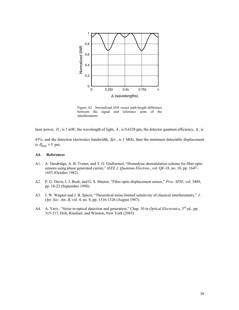
0 0.25λ 0.5λ 0.75λ λ0
0.2
0.4
0.6
0.8
1
∆ (wavelengths)
Nor
mal
ized
SN
R
Figure A2. Normalized SNR versus path-length difference between the signal and reference arms of the interferometer.
laser power, , is 1 mW, the wavelength of light, lP λ , is 0.6328 µm, the detector quantum efficiency, η , is 45%, and the detection electronics bandwidth, ν∆ , is 1 MHz, then the minimum detectable displacement is 5min =δ pm. A4. References A1. A. Dandridge, A. B. Tveten, and T. G. Giallorenzi, “Homodyne demodulation scheme for fiber optic
sensors using phase generated carrier,” IEEE J. Quantum Electron., vol. QE-18, no. 10, pp. 1647-1653 (October 1982).
A2. P. G. Davis, I. J. Bush, and G. S. Maurer, “Fiber optic displacement sensor,” Proc. SPIE, vol. 3489,
pp. 18-22 (September 1998). A3. J. W. Wagner and J. B. Spicer, “Theoretical noise-limited sensitivity of classical interferometry,” J.
Opt. Soc. Am. B, vol. 4, no. 8, pp. 1316-1326 (August 1987). A4. A. Yariv, “Noise in optical detection and generation,” Chap. 10 in Optical Electronics, 3rd ed., pp.
315-317, Holt, Rinehart, and Winston, New York (2985).
30


