Download - Solving the ESD challenges in SOI technology

BART KEPPENS
SEPTEMBER 2015
On-chip ESD solutions for
SOI technology

Intellectual Property
SOFICS © 2015 Proprietary & Confidential 2
As is the case with many published ESD design solutions, the techniques and protection solutions described in this presentation are protected by patents
and patents pending and cannot be copied freely.
Contact Sofics to discuss about a license for the Sofics technology.
PowerQubic, TakeCharge, and Sofics are trademarks of Sofics BVBA.
SOFICS © 2015 Proprietary & Confidential 3
Outline
• Introduction
– SOI technology
– Advantages of SOI compared to bulk
– Promotion
• Challenges for ESD protection
• Solutions
• Conclusion

Silicon On Insulator (SOI)
SOFICS © 2015 Proprietary & Confidential 4
• Electrically isolate layer of silicon from the rest of the silicon wafer

Silicon On Insulator (SOI) advantages
SOFICS © 2015 Proprietary & Confidential 5
• Higher performance
– Reduced junction capacitance
– Boosting effect of floating body
• Lower power
– Supply voltage reduction options
– Reduced junction capacitance
• Area savings
– No wells, no taps, no latch-up denser layout
• High reliability
– Reduced susceptibility to Electro-magnetic interference
– No latch-up problems
– Able to withstand higher temperatures
– Radiation hard

Silicon On Insulator (SOI) promotion
SOFICS © 2015 Proprietary & Confidential 6

SOFICS © 2015 Proprietary & Confidential 7
Outline
• Introduction
• Challenges for ESD protection
– ESD Design window reduction in Advanced CMOS
– Floating, isolated body for each MOS finger/segment
– Self-heating
– Strongly reduced ESD performance for basic ESD elements
– Layout constraints for typical ESD devices
• Solutions
• Conclusion

SOFICS © 2015 Proprietary & Confidential 8
Advancing CMOS – new ESD challenges!
[Groeseneken, IEW 2008]

ESD Design Margin evaporates for advanced CMOS
SOFICS © 2015 Proprietary & Confidential 9
• Decreasing solution space
– Normal operation (VDD)
Slight decrease
– Maximum voltage decreases rapidly
Transient breakdown of gate oxides
Burn-out of output drivers
Core failure voltage
– Difference = ESD design window
Rapid reduction of design margins
0 5 10 15 20 25
Node [nm]
V [V]
Maximum voltage Vdd
500
350
250
180 130
90 65 45
ESD design window
45nm/40nm: ESD design space reduced to 3V!

Process scaling – ESD design window
SOFICS © 2015 Proprietary & Confidential 10
• A. Salman (AMD), R. Gauthier (IBM), 2001
– “Historically, the failure mode of the nMOS due is source-to-drain filamentation, ... However, as the gate-oxide thickness shrinks, the ESD failure changes over to oxide breakdown.”
[Salman, 2001]
N+ P+ N+
Vss
Sub D S G

Impact on ESD protection strategy
Power Clamp Resistance of
Vdd, Vss bus
line
Diode
V
I
V
I
GOX damage
Vmin Vmax
ESD Spec.
V
I
V
I
Robustness: OK
Effectiveness: NOT OK
Vdd
Vss
IN +
SOFICS © 2015 Proprietary & Confidential 11

Low Core breakdown voltages - SOI
SOFICS © 2015 Proprietary & Confidential 12
• Example: Core breakdown measurements 90nm SOI
– Different gate connection options analyzed
– Absolute Vmax ~3.6V
For 90nm Bulk ~ 4.05 – 4.6V (measured in TSMC process)
10-12
10-10
10-8
10-6
10-4
0 1 2 3 4 5 6
VSS typ(LVt/MVt)VSS SS(MVt/HVt)VSS FF(MVt/HVt)VDD typ(LVt/MVt)VDD SS(MVt/HVt)VDD FF(MVt/HVt)
leakage c
urr
ent [A
] @
1.3
2V
voltage [V]
Vdd
Vss
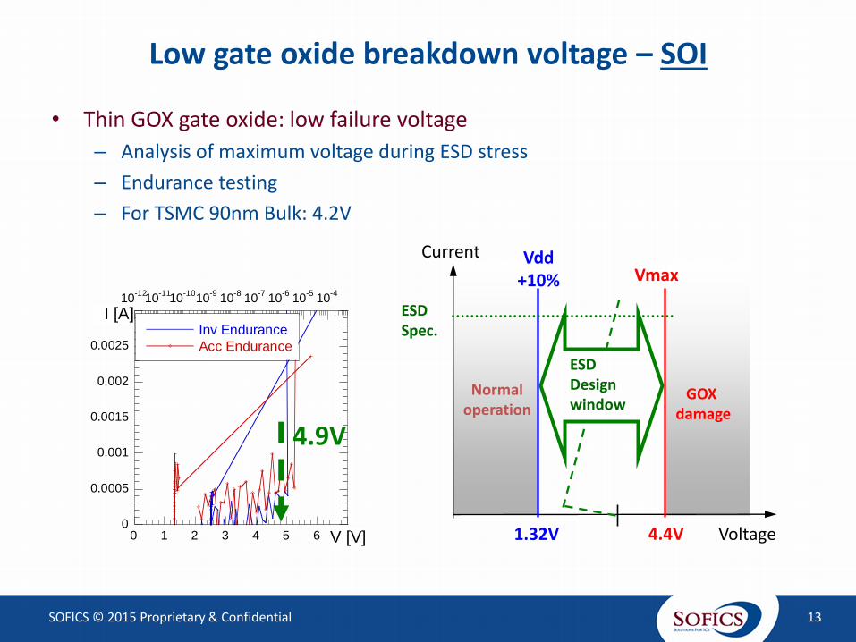
Low gate oxide breakdown voltage – SOI
SOFICS © 2015 Proprietary & Confidential 13
• Thin GOX gate oxide: low failure voltage
– Analysis of maximum voltage during ESD stress
– Endurance testing
– For TSMC 90nm Bulk: 4.2V
0
0.0005
0.001
0.0015
0.002
0.0025
0.003
0 1 2 3 4 5 6 7
10-12
10-11
10-10
10-9
10-8
10-7
10-6
10-5
10-4
Inv Endurance
Acc Endurance
I [A]
V [V]
4.9V
Current
GOX damage
Normal operation
ESD Design window
Vdd +10% Vmax
ESD Spec.
1.32V 4.4V Voltage

SOI MOS – Lower intrinsic current capability
SOFICS © 2015 Proprietary & Confidential 14
• High thermal resistance of buried oxide layer
– SOI has lower intrinsic current capability
• Ballasting is often used to increase ESD protection
– Make Vt2 > Vt1 to make sure all fingers trigger
– BUT: Ballasting less effective for SOI
Due to reduced intrinsic current capability
Example: voltage across 5 ohm resistance, W = 100 um
Bulk process:
– It2 ~ 9 mA/um (typical value)
>> Voltage across resistor: 900 mA x 5 Ohm = 4.5V
SOI process
– It2 ~ 2 mA/um (typical value)
>> Voltage across resistor: 200 mA x 5 Ohm = 1V

Sensitive MOS transistors – SOI
SOFICS © 2015 Proprietary & Confidential 15
• HV output drivers (NMOS)
– Failure at snapback
– Silicided or silicide blocked devices
0
0.02
0.04
0.06
0.08
0.1
0 2 4 6 8 10
10-12
10-10
10-8
10-6
10-4
curr
ent [A
]
voltage [V]
leakage current [A] @ 3.63V
0
0.02
0.04
0.06
0.08
0.1
0.12
0.14
0 2 4 6 8 10
10-9
10-8
10-7
10-6
10-5
10-4
10-3
cu
rre
nt [A
]
voltage [V]
leakage current [A] @ 3.63V
Fully silicided
Silicide blocked

Background: NMOS in bulk technology
SOFICS © 2015 Proprietary & Confidential 16
• NMOS in bulk technology has a shared P-substrate
– Shared substrate helps to trigger all fingers
– Vt1 of second/third/… finger is reduced due to biased bulk
N+
gnd
P+ STI N+
source drain
N+
gnd
P+ STI N+
source drain
...
shared p-substrate substrate current
substrate current
Background: Influence of the bulk resistance
SOFICS © 2015 Proprietary & Confidential 17
• Effect of effective substrate resistance on NMOS performance
– Small size MOS fails at snapback
– Guard-band too close to base region of parasitic NPN
0
0.02
0.04
0.06
0.08
0.1
0 2 4 6 8
10-12
10-11
10-10
10-9
10-8
10-7
10-6
cu
rre
nt [A
]
voltage [V]
leakage current [A] @ 3.63V

Background: Influence of the bulk resistance
SOFICS © 2015 Proprietary & Confidential 18
• Effect of effective substrate resistance on NMOS performance
– Large size NMOS survives snapback
– Effective substrate resistance in center of MOS is much higher
0
0.5
1
1.5
2
0 2 4 6 8
10-12
10-11
10-10
10-9
10-8
10-7
10-6
curr
ent [A
]
voltage [V]
leakage current [A] @ 3.63V

Background: SOI MOS has isolated body regions
SOFICS © 2015 Proprietary & Confidential 19
• Body regions are isolated
– No body potential coupling between (adjacent) fingers
N+ STI N+
source drain
N+ STI N+
source drain
...
shared p-substrate
BOX
A
A’

Metallization trends
SOFICS © 2015 Proprietary & Confidential 20
• 2 distinct groups of metallization
– Local Metals
Decreased of thickness over 400 %
– Top metal
Thickness hardly changed over the technologies

Conclusion
SOFICS © 2015 Proprietary & Confidential 21
• 28nm SOI will have very weak intrinsic ESD behavior
– Low Core breakdown
– Low gate oxide breakdown
– Low to no ESD current through MOS
LV MOS fails in 28nm TSMC, despite Silicide block
HV MOS fails in 90nm SOI, despite Silicide block
• SOI devices have low intrinsic failure current
– Typically It2SOI ~ It2bulk / 4
– Diodes have highest It2 in SOI
• Improved solutions needed
0
10
20
30
40
50
60
70
NMOS DIODE SCR
130 nm bulk65 nm bulk130 nm SOI65 nm SOI
It2 (
mA
/um
)

Confirmation by industry
SOFICS © 2015 Proprietary & Confidential 22
• GlobalFoundries
“Deeply scaled PD- and FD-SOI require new approaches to ESD protection.”
Reduction of MOSFET oxide and junction breakdown voltage
Reduced diode current shunting capability
Increased interconnect resistivity.
“SOI technology presents some distinctive challenges to ESD design.”
Vertical and deep body ESD structures infeasible.
Lateral SOI diode based (“rail-based”) protection approach is less effective
Excessive voltage build-up along the ESD path involving power buses, power-clamps (Pclamp), and diodes.
• ST Microelectronics
“Despite its numerous advantages, developing a complete ESD protection network in a pure FDSOI CMOS technology remains very challenging due to the presence of the buried oxide (BOX), which either forbids the use or significantly degrades the ESD performance of basic ESD devices.”

SOFICS © 2015 Proprietary & Confidential 23
Outline
• Introduction
• Challenges for ESD protection
• Solutions
– GlobalFoundries, STMicroelectronics
– Sofics IP
• Conclusion
Solution presented by GlobalFoundries
SOFICS © 2015 Proprietary & Confidential 24
• The pad-based “local clamping” scheme is a promising option.
– ESD device directly between the pad and Vss
– ESD current flows from pad to ground without going through the resistive path and the Pclamp. This way, the pad voltage is considerably reduced, expanding the design space.

Solution presented by GlobalFoundries
SOFICS © 2015 Proprietary & Confidential 25
• Confirmation of ESD challenge
– Dual diode based ESD concept not possible to advanced SOI-CMOS
– Local pad-Ground protection concept required
• SCR type protection concept
– High impedance during functional operation
– PIN diode during ESD stress
http://www.advancedsubstratenews.com/2011/05/esd-protection-for-advanced-soi/

Solution presented by ST Microelectronics
SOFICS © 2015 Proprietary & Confidential 26
• Hybrid SOI – bulk technology
– Combine best of both worlds

Bulk NMOS vs Hybrid NMOS vs SOI NMOS
SOFICS © 2015 Proprietary & Confidential 27
• TLP analysis of NMOS devices
– Maximum current capability is degraded (divided by 2.8) in SOI
– Hybrid Bulk and Bulk performances are very similar.
– Significant triggering voltage reduction observed in SOI
Lower electrostatic control of the un-doped base.

Hybrid solution: use bulk device to protect SOI
SOFICS © 2015 Proprietary & Confidential 28
• ST Microelectronics has combined bulk and SOI
– ESD devices created in hybrid-bulk section
– Core devices and IO drivers are created in SOI section

Hybrid solution: use bulk device to protect SOI
SOFICS © 2015 Proprietary & Confidential 29
• ST Microelectronics has combined bulk and SOI
– ESD devices created in hybrid-bulk section
– Core devices and IO drivers are created in SOI section

Sofics’ TakeCharge ESD expertise in SOI
SOFICS © 2015 Proprietary & Confidential 30
• Succesfull TakeCharge portings in 130nm, 90nm and 65nm
– TakeCharge solutions can be transferred to SOI
Most solutions work in both SOI and BULK
Additional patents to solve specific SOI issues
Patents portable to SOI
SCR patents
DT-SCR, GG-SCR, RT- SCR ...
Design window enlargements
ASP, rubber band, enhanced rubber band
SOI specific Technical know-how
For example: technique to minimize area
SOI specific Patents
Cascode MOS In SOI (1997) (not used anymore)
SCR in SOI (2003)
Bulk coupling for MOS (2005)
Sofics IP in SOI

Sofics experience on SOI
SOFICS © 2015 Proprietary & Confidential 31
• Sofics experience in SOI applications
Application CMOS node
High temperature, High voltage 1um
General digital, analog and high temperature 130nm (PD)
LNA 130nm (PD)
Computing platform 90nm (BST)
High performance computing 65nm (PD)

Analysis of diode structures
SOFICS © 2015 Proprietary & Confidential 32
• Diodes
– Basic building blocks for ESD protection
– Required in almost all pin combinations
• Sofics’ SOI analysis
– Optimization of diode structure
Low capacitive
Small area
High ESD failure current
Low on-resistance
– Different diode types studied
NO-STI diode
Gated diode

NO-STI vs. Gated diodes
SOFICS © 2015 Proprietary & Confidential 33
• NO-STI diode
– Larger LAC: mask misalignment, depletion regions, out-diffusions
– Y: mask-misalignment
– Higher series resistance
– Relatively large in size
• Gated diode
– Smaller LAC: MDR gate length
– Oxide reliability has to be watched
– Minimum resistance
– Compact area
BOX
P+ N+
LAC Y Y
BOX
P+ N+
LAC

NO-STI vs. Gated diodes
SOFICS © 2015 Proprietary & Confidential 34
• NO-STI diode
– It2 per perimeter ~ 6.5mA/um
– It2 per area ~ 3 mA/um²
• Gated diode
– It2 per perimeter ~ 9.2 mA/um
– It2 per area ~ 10.9 mA/um²
0
0.5
1
1.5
2
2.5
3
0 0.5 1 1.5 2
curr
ent [A
]
voltage [V]
0
0.5
1
1.5
2
2.5
3
0 0.5 1 1.5 2
cu
rre
nt [A
]
voltage [V]
Improvement: 3x Performance per area 6x lower On resistance

Analysis of MOS structures
SOFICS © 2015 Proprietary & Confidential 35
• MOS
– Self-protective output drivers
Maximize It2 per area
– Non-self protective output drivers
Maximize design window (Vt2)
• Sofics’ SOI analysis
– Optimisation of MOS structure for ESD improvement
– Investigation of failure voltage and current
Influence of silicide block
Influence of layout style
New layout approaches to boost performance

MOS structures
SOFICS © 2015 Proprietary & Confidential 36
• MOS devices in SOI have low ESD performance
– Often < 1mA/um
– Adding ballasting (Silicide block) does not always improve this
• MOS based ESD protection is difficult
– Not suitable as clamp
– Difficult to make self-protective drivers
• Still improvements exist
– Sofics’ proprietary technique explained in next slides
N+ STI N+
source drain
N+ STI N+
source drain
...
shared p-substrate BOX
0
0.02
0.04
0.06
0.08
0.1
0 2 4 6 8 10
10-12
10-10
10-8
10-6
10-4
curr
ent [A
]
voltage [V]
leakage current [A] @ 3.63V

Performance improvement through layout
SOFICS © 2015 Proprietary & Confidential 37
• ESD performance on 90 nm PD SOI
• Fully silicided 1.2V NMOS devices
– Reference NMOS1
Standard fully silicided MOS driver
Low performance (0.75 mA/um)
Large statistical variation
– NMOS1-special layout
Proprietary layout technique
Much higher performance (1.58 mA/um)
0
0.2
0.4
0.6
0.8
1
0 0.5 1 1.5 2 2.5 3 3.5
10-9
10-8
10-7
10-6
10-5
10-4
10-3
NMOS1_refNMOS1 special
cu
rre
nt [A
]
voltage [V]
leakage current [A] @ 1.32V
Fully Silicided
Imp
rove
me
nt:
2
x P
erf
orm
ance

MOS performance improvement options
SOFICS © 2015 Proprietary & Confidential 38
• Traditional solution
– Silicide blocked drain junction
– Optimal DCGS = 1um
• Sofics approach
– Proprietary layout technique
– Lower Vt1 (Uniform triggering)
– Larger Vt2 (Larger design window)
0
0.5
1
1.5
2
2.5
3
0 1 2 3 4 5 6
cu
rre
nt [A
]
voltage [V]
0
0.5
1
1.5
2
2.5
3
0 1 2 3 4 5 6
curr
ent [A
]
voltage [V]
Improvement: 2x Performance per area
Lower on resistance

Example: GOX 1 FS NMOS in SOI
SOFICS © 2015 Proprietary & Confidential 39
• Restore body coupling in PD SOI process
– Special layout technique: Vertical poly stripes enable body coupling in PD SOI
Body coupling restored!
– Performance significantly improved
Other variations exist
0
0.4
0.8
1.2
1.6
0 1 2 3 4 5 6 7 8
It2 [m
A/u
m]
vertical poly stripe spacing [um]
Sofics patent Specific for SOI

What about SCR’s?
SOFICS © 2015 Proprietary & Confidential 40
• SCR’s used a lot in bulk CMOS for ESD protection
– Low parasitic capacitance
– Small area
– Low leakage
– High ESD robustness
– Low voltage clamping for sensitive device protection
– ...
• Is it possible to use SCR’s in SOI technology?

Is it possible to design SCRs in SOI?
SOFICS © 2015 Proprietary & Confidential 41
• Basic SCR structure in Bulk technology
N+ P+ P+ N+
G2 G1
P+ P+ N+ N+ STI STI STI
Cathode Anode
STI STI

Is it possible to design SCRs in SOI?
SOFICS © 2015 Proprietary & Confidential 42
• Basic SCR structure in SOI technology
N+ P+ P+ N+
G2 G1
P+ P+ N+ N+ STI STI STI
Cathode Anode
STI STI
BOX

Constructing SCR in SOI (1/3)
SOFICS © 2015 Proprietary & Confidential 43
• Step 1: remove STI between junctions – create active area without implant
STI STI
BOX
P+ N+ Nwell Pwell
LAC STI STI
BOX
LAC
Silicide
P+ N+
Active Area
Pwell Nwell
Sofics patent Specific for SOI

Constructing SCR in SOI (2/3)
SOFICS © 2015 Proprietary & Confidential 44
• Step 2: Create G1/G2 – Segmented layout style
STI
Anode Anode G2
G1 Cathode Cathode
Pwell
Nwell Silicided Active
Sofics patent Specific for SOI

Constructing SCR in SOI (3/3)
SOFICS © 2015 Proprietary & Confidential 45
• Step 3: Isolate regions – Apply Silicide block pattern
STI
Anode Anode G2
G1 Cathode Cathode
Silicide Block
Sofics patent Specific for SOI

Ultra low voltage clamping through SCR’s
SOFICS © 2015 Proprietary & Confidential 46
• GOX1 NMOS
– Holding voltage = 2.8V
• DT-SCR
– Holding voltage of 1V
– Extra margin for voltage drop over bus resistance
0
0.5
1
1.5
2
0 0.5 1 1.5 2 2.5 3 3.5 4
cu
rre
nt [A
]
voltage [V]
W=8x30um Vt1 = 3.2V
0
0.5
1
1.5
2
0 0.5 1 1.5 2 2.5 3 3.5 4
curr
ent [A
]
voltage [V]
Improvement: Lower clamping voltage possible
Sofics patent Specific for SOI

Confirmation by industry
SOFICS © 2015 Proprietary & Confidential 47
• IBM also believes in SCR concepts for SOI
“Silicon-Controlled Rectifier (SCR) devices are widely used in advanced CMOS technologies for on-chip ESD protection. Advantages of SCR devices include small footprint, low leakage and low capacitance.”
EOS/ESD 2013 – JunJun Li, IBM
Sofics Diode triggered SCR patent

Conclusion
SOFICS © 2015 Proprietary & Confidential 48
• Many challenges for ESD protection in SOI process
– Narrow design window for core protection
– Extremely sensitive MOS devices
– Sensitive thin gate oxide (GOX1)
– Low robustness, high Ron for standard ESD diodes
• TakeCharge® solutions
– Diode improvement: larger performance per area
– Various MOS robustness improvements
– Low voltage clamping with Silicon Controlled Rectifiers (SCR)

Contact us for more information?
SOFICS © 2015 Proprietary & Confidential 49
Sofics website
SOI cases


