Applications
• Curing
• Adhesives
• Inks
• PlasticProducts
• WoodFinish
• Photocatalyticair/waterpurification
• Analyticinstrumentation
• Medical
• Diagnostics
• FluorescenceImaging
Features:• HighPowerUVLEDwithPeakWavelengthsbetween365-405nm
• Industrystandard3.5mmx3.5mmpackage
• 130°viewingangleat50%Iv
• LowThermalResistance-3.4C/W
• Built-inESDProtection
• RoHSandREAChcompliant
Table of ContentsSST-10BinningStructure. . .2
ProductShipping&LabelingInformation. . . . . . . . . . . . . . . .3
OpticalandElectricalCharacteristics. . . . . . . . . . . . .4
MechanicalDimensions. . . .6
TapeandReel. . . . . . . . . . . . . .7
SolderingProfile. . . . . . . . . . .8
PrecautionsforUse. . . . . . . . .9
HistoryofChanges. . . . . . . 10
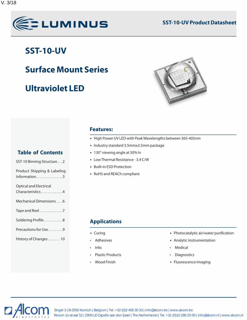
SST-10-UV
Surface Mount Series
Ultraviolet LED
SST-10-UV Product Datasheet
V. 3/18
Singel 3 | B-2550 Kontich | Belgium | Tel. +32 (0)3 458 30 33 | [email protected] | www.alcom.beRivium 1e straat 52 | 2909 LE Capelle aan den Ijssel | The Netherlands | Tel. +31 (0)10 288 25 00 | [email protected] | www.alcom.nl

Luminus Devices, Inc.•T978.528.8000•www.luminus.com175NewBostonStreet•Woburn,MA01801
SST-10 Binning Structure
SST-10UVLEDsaretestedforluminousfluxandchromaticityatadrivecurrentof500mA-20mssinglepulseandplacedintooneofthefollowingluminousflux(F)andchromaticity(WWW)bins:
FluxBin(F) MinimumFlux(mW) MaximumFlux(mW)
E 720 810
F 810 900
G 900 990
H 990 1080
I 1080 1170
Flux Bins - Test condition=500mA, 250C, 20ms pulse
WavelengthBin(WWW) MinimumWavelength(nm) MaximumWavelength(nm)
365 365 370
370 370 375
380 380 385
385 385 390
390 390 395
395 395 400
400 400 405
405 405 410
Wavelength Bins - Test condition=500mA, 250C, 20ms pulse
*Note: Luminusmaintainsa+/-6%toleranceonfluxmeasurements.
Ordering Information
Products Ordering Part Number Description
SST-10-UV-A130 SST-10-UV-A130-FWWW-NNHighPower1-mm2UVLEDina3535surfacemountpackagewitha130degreemoldedlens
SST-10-UV Product Datasheet
2PDS-002674 Rev 01 © 2016 Luminus Devices, Inc. - All Rights Reserved

Luminus Devices, Inc.•T978.528.8000•www.luminus.com175NewBostonStreet•Woburn,MA01801
Part Number Nomenclature
Product Family LED Emission Area Color Package Configuration Bin kit
SST:SurfaceMountPackage 10:1.0mm2 <C>:Color
U=Ultraviolet A130:130-degreelensFluxandWavelengthbinkitcode-Seeavailableordering
codesbelow
SST 10 <C> <A###> <FF###>
SST-10 Bin Kit Order Codes
ThefollowingtabledescribesthebinkitorderingcodesavailablefortheSST-10UVLEDs.Eachbinkitspecifiesaminimumfluxaswellasspecificchromaticitybinsallowed.PleasenotethatwithineachkitamaximumfluxisnotspecifiedandasaresultLuminusmayshipanypartmeetingorexceedingtheminimumfluxspecification.Shipmentswillalwaysmeetthelistedchromaticitybins.Forinformationonorderingbinkitsnotlistedbelow,pleasecontactLuminus.
SST-10 UV Bin Kit Order Codes
WavelengthRangeLuminousFlux
ChromaticityBins KitNumberBinKitFluxCode
Min.Flux
365 E 720 365, 370 E365-00
385 G 900 380, 385 G385-00
395 G 900 390, 395 G395-00
405 F 810 400, 405 F405-00
Product Shipping & Labeling Information
AllSST-10productsarepackagedandlabeledwiththeirrespectivebinasoutlinedinthetablesonpages2&3.Eachreelwillonlycontainonebin.
SST-10 UV
Product Family LED Emission Area Color Package Configuration Bin kit
SST:SurfaceMountPackage 10:1.0mm2 Color A130:130-degreelens FluxandChromaticitybinkit
codeasoutlinedabove
SST 10 UV AXXX FWWW
SST-10-UV Product Datasheet
3PDS-002674 Rev 01 © 2016 Luminus Devices, Inc. - All Rights Reserved

(Part #) Product Datasheet
Note 1: Ratings are based on operation at a constant junction temperature of Tj = 25ºC.
Note 2: To prevent damage, please refer to operating conditions and derating curves for appropriate maximum operating conditions
Note 3: Maximum operating case temperature combined with maximum drive current defines the total maximum operating condition for the device. To prevent damage, please follow derating curves for all operating conditions.
Note 4: Luminus SST-10-UV LEDs are designed for operation up to an absolute maximum forward drive current as specified above. Product lifetime data is specified at typical forward drive currents. Sustained operation at absolute maximum currents will result in a reduction of device lifetime compared to typical forward drive currents. Actual device lifetimes will also depend on junction temperature. Refer to the current vs. junction temperature derating curves for further information. In pulsed operation, rise time from 10-90% of forward current should be larger than 0.5 microseconds.
Note 5: Caution must be taken not to stare at the light emitted from these UV LEDs.
Optical and Electrical Characteristics at 500mA
Parameter SymbolPackage Type
UnitA130-365 A130-385 A130-395 A130-405
ForwardCurrent2 If 500 500 500 500 mA
MaximumCurrent Imax 1000 1000 1000 1000 mA
OutputPowerTypical Φr 875 1015 1015 930 mW
minVoltage Vmin 3.0 3.0 3.0 3.0 V
ForwardVoltageTyp. Vf 3.6 3.4 3.4 3.4 V
maxVoltage Vmax 4.0 4.0 4.0 4.0 V
ViewingAngle 2Ø1/2 120 120 120 120 degrees
PeakWavelengthTyp. λP 365 385 395 405 nm
FWHMat50%ofΦ Δλ1/2 10 10 10 10 nm
ThermalRes.(Electrical) RTH 2.3 2.3 2.3 2.3 °C/W
Absolute Maximum Ratings
Parameter Symbol Rating Unit
ReverseVoltage Vr 5 V
StorageTemperature TsTG -40~100 °C
JunctionTemperature Tj 100 ºC °C
SolderingTemperature Tsld JEDEC020C,260ºC
ESDSensitivity(HBM) Vb 6000 V
Luminus Devices, Inc.•T978.528.8000•www.luminus.com175NewBostonStreet•Woburn,MA01801
SST-10-UV Product Datasheet
Optical and Electrical Characteristics
4PDS-002674 Rev 01 © 2016 Luminus Devices, Inc. - All Rights Reserved

(Part #) Product Datasheet
Relative Output Flux vs. Forward Current Change in Voltage vs. Forward Current
Luminus Devices, Inc.•T978.528.8000•www.luminus.com175NewBostonStreet•Woburn,MA01801
SST-10-UV Product Datasheet
Optical and Electrical Characteristics
Typical Spectrum Typical Polar Radiation Plot
Change in Wavelength vs. Forward Current Change in FWHM vs Forward Current
0.00
0.50
1.00
1.50
2.00
2.50
3.00
0.00 0.50 1.00 1.50
Rela
tive
Pow
er
If - Forward Current [Amps]
Relative Power vs Forward Current (If)
-1.00
-0.75
-0.50
-0.25
0.00
0.25
0.50
0.75
1.00
0.00 0.50 1.00 1.50
Chan
ge in
For
war
d Vo
ltage
[Vol
ts]
If - Forward Current [Amps]
Change in Forward Voltage (Vf) vs Forward Current (If)
-0.80
-0.60
-0.40
-0.20
0.00
0.20
0.40
0.60
0.80
0.00 0.50 1.00 1.50
Chan
ge in
Cen
troi
d W
avel
engt
h (λ
c)
If - Forward Current [Amps]
Change in Wavelength (λp) vs Forward Current (If)
-1.00
-0.75
-0.50
-0.25
0.00
0.25
0.50
0.75
1.00
0.00 0.50 1.00 1.50
Chan
ge in
Ful
l-Wid
th H
alf-M
axim
um [
nm]
If - Forward Current [Amps]
Change in Full-Width Half-Maximum vs Forward Current (If)
5PDS-002674 Rev 01 © 2016 Luminus Devices, Inc. - All Rights Reserved
0.2
0.4
0.6
0.8
1.0
0 20° 40° 60° 80°0.20.40.60.81.0
0°10°20°
30°
40°
50°
60°
70°
80°
90°

1.0.040
DIE EMITTING AREA
3.45+-.20.00
.136+-.008.000
1.1.041
3.45+-.20.00
.136+-.008.000
1.38.054
1.38.054
E
EDIE EMITTING
AREA
.15[.006] M A BCENTER OF DIE EMITTING AREAA
.64±.13.025±.005
BACK OF SUBSTRATETO TOP OF DIEEMITTING AREA
2.60.102
1.88±.13.074±.005
.58±.06.023±.002
R.2.006
SECTION E-E
B
3.25.128
1.30.051
.10.004
2.30.091
3.25.128
ANODE
THERMAL PAD(NEUTRAL)
CATHODE
3.25.128
1.30.051
2.30.091
3.25.128
RECOMMENDED SOLDER PAD LAYOUT
D
C
B
AA
B
C
D
12345678
8 7 6 5 4 3 2 1
X = 0.5mm.X = 0.127mm.XX = 0.050mm.XXX = 0.010mm
18/1
DRAWING, OUTLINE, 002848, SST-10-UV, 120°
S.KEDDIE
175 NEW BOSTON STREETWOBURN, MA 01801
978-528-8000DESCRIPTION:
P01SURFACES0.8 MICRONS
UNLESS OTHERWISE SPECIFIED TOLERANCES ARE MILLIMETERS [INCHES]
This document and its contentsare confidential information of
Luminus Devices, Inc. Copyright 2005 Luminus Device,Inc.
All rights reserved.
B SCALE:
ENGINEER: NUMBER:DRAFTER:
SIZE: REV:1 OF 1DIMENSIONS ARE IN (UNLESS OTHERWISE SPECIFIED): SHEET:
DWG-002848
BYSKK
ECO DESCRIPTION OF CHANGE DATEREVP01 INITIAL DESIGN CONCEPT. 2/29/16
REVISION HISTORY
ANGLES 0.5
PROPRIETARY ANDCONFIDENTIAL
-
Mechanical Dimensions
130-degree lens option
Luminus Devices, Inc.•T978.528.8000•www.luminus.com175NewBostonStreet•Woburn,MA01801
SST-10-UV Product Datasheet
1.0.040
DIE EMITTING AREA
3.45+-.20.00
.136+-.008.000
1.1.041
3.45+-.20.00
.136+-.008.000
1.38.054
1.38.054
E
EDIE EMITTING
AREA
.15[.006] M A BCENTER OF DIE EMITTING AREAA
.64±.13.025±.005
BACK OF SUBSTRATETO TOP OF DIEEMITTING AREA
2.60.102
1.88±.13.074±.005
.58±.06.023±.002
R.2.006
SECTION E-E
B
3.25.128
1.30.051
.10.004
2.30.091
3.25.128
ANODE
THERMAL PAD(NEUTRAL)
CATHODE
3.25.128
1.30.051
2.30.091
3.25.128
RECOMMENDED SOLDER PAD LAYOUT
D
C
B
AA
B
C
D
12345678
8 7 6 5 4 3 2 1
X = 0.5mm.X = 0.127mm.XX = 0.050mm.XXX = 0.010mm
18/1
DRAWING, OUTLINE, 002848, SST-10-UV, 120°
S.KEDDIE
175 NEW BOSTON STREETWOBURN, MA 01801
978-528-8000DESCRIPTION:
P01SURFACES0.8 MICRONS
UNLESS OTHERWISE SPECIFIED TOLERANCES ARE MILLIMETERS [INCHES]
This document and its contentsare confidential information of
Luminus Devices, Inc. Copyright 2005 Luminus Device,Inc.
All rights reserved.
B SCALE:
ENGINEER: NUMBER:DRAFTER:
SIZE: REV:1 OF 1DIMENSIONS ARE IN (UNLESS OTHERWISE SPECIFIED): SHEET:
DWG-002848
BYSKK
ECO DESCRIPTION OF CHANGE DATEREVP01 INITIAL DESIGN CONCEPT. 2/29/16
REVISION HISTORY
ANGLES 0.5
PROPRIETARY ANDCONFIDENTIAL
-
6PDS-002674 Rev 01 © 2016 Luminus Devices, Inc. - All Rights Reserved

Tape and Reel
Luminus Devices, Inc.•T978.528.8000•www.luminus.com175NewBostonStreet•Woburn,MA01801
SST-10-UV Product Datasheet
7PDS-002674 Rev 01 © 2016 Luminus Devices, Inc. - All Rights Reserved

Luminus Devices, Inc.•T978.528.8000•www.luminus.com175NewBostonStreet•Woburn,MA01801
SST-10-UV Product Datasheet
Soldering Profile
ProfileFeature Sn-PbEutecticAssembly Pb-FreeAssembly
Preheat&SoakTemperaturemin(Tsmin)Temperaturemax(Tsmax)Time(TsmintoTsmax)(ts)
100°C150°C
60-120seconds
150°C200°C
60-120seconds
Averageramp-uprate(TsmaxtoTp) 3°C/secondmax 3°C/secondmax
Liquidoustemperature(TL)Timeatliquidous(tL)
183°C60-150seconds
217°C60-150seconds
Peakpackagebodytemperature(Tp)* 230 °C ~235 °C 255 °C ~260 °C
Classificationtemperature(Tc) 235°C 260 °C
Time(tp)within5°Cofthespecifiedclassificationtemperature(Tc)
20seconds 30seconds
Averageramp-downrate(TptoTsmax) 6°C/secondmax 6°C/secondmax
Time25°Ctopeaktemperature 6minutesmax 8minutesmax
*Toleranceforpeakprofiletemperature(Tp)isdefinedasasupplierminimumandausermaximum.**Tolerancefortimeatpeakprofiletemperature(tp)isdefinedasasupplierminimumandausermaximum.
8PDS-002674 Rev 01 © 2016 Luminus Devices, Inc. - All Rights Reserved
Luminus Devices, Inc.•T978.528.8000•www.luminus.com175NewBostonStreet•Woburn,MA01801
SST-10-UV Product Datasheet
Storage:
1.BeforeopeningthepackageTheLEDsshouldbekeptatatemperaturelowerthan40°Candrelativehumiditylowerthan90%.TheLEDsshouldbeusedwithinayear.WhenstoringtheLEDs,moistureproofpackagewithabsorbentmaterial(silicagel)isrecommended.
2.Afteropeningthepackage
TheLEDsshouldbekeptattemperaturelowerthan30°Candrelativehumiditylowerthan60%.TheLEDsshouldbesolderedwithin168hours(7days)afteropeningthemoistureproofpackage.
IfunusedLEDsremain,theyshouldbestoredinmoistureproofpackages,suchassealedcontainerswithmoistureproofpackagewithinabsorbentmaterial(silicagel).ItisalsorecommendedtoreturntheunusedLEDstotheoriginalmoistureproofpackageandtosealthemoistureproofpackageagain.
Ifthemoistureabsorbentmaterial(silicagel)vaporsorexpirestheexpirationdate,bakingtreatmentshouldbeperformedbyusingthefollowingconditions:60°Cfor20hours.
TheLEDselectrodeandleadframecompriseasilverplatedcopperalloy.Thesilversurfacemaybeaffectedbyenvironments.PleaseavoidconditionswhichmaycausetheLEDstocorrodeordiscolore.Thecorrosionordiscolorationmightlowersolderabilityoraffectopticalcharacteristics.
Pleaseavoidrapidtransitioninambienttemperature,especiallyinhighhumidityenvironmentswherecondensationcanoccur.
Static Electricity:
1.Theproductsaresensitivetostaticelectricity,andcareshouldbetakenwhenhandlingthem.
2.StaticelectricityorsurgevoltagewilldamagetheLEDs.Itisrecommendedtowearaanti-electrostaticwristbandoranti-electrostat-icgloveswhenhandlingtheLEDs.
3.Alldevices,equipmentandmachinerymustbeproperlygrounded.Itisrecommendedthatmeasuresbetakenagainstsurgevolt-agetotheequipmentthatmountstheLEDs.
Precautions for Use
9PDS-002674 Rev 01 © 2016 Luminus Devices, Inc. - All Rights Reserved

SST-10-UV Product Datasheet
History of Changes
Rev Description of Change
01 07/12/2016 InitialRelease-ProductionSpecifications
Singel 3 | B-2550 Kontich | Belgium | Tel. +32 (0)3 458 30 33 | [email protected] | www.alcom.beRivium 1e straat 52 | 2909 LE Capelle aan den Ijssel | The Netherlands | Tel. +31 (0)10 288 25 00 | [email protected] | www.alcom.nl
![A Dimensions: [mm] B Recommended land pattern: [mm] D ... · 2005-12-16 DATE SSt SSt SSt SSt SSt SSt SSt BY SSt SSt SMu SMu SSt ... RDC Value 600 800 1000 0.20 High Cur rent ... 350](https://cdn.vdocument.in/doc/165x107/5c61318009d3f21c6d8cb002/a-dimensions-mm-b-recommended-land-pattern-mm-d-2005-12-16-date-sst.jpg)
![A Dimensions: [mm] B Recommended land pattern: [mm] D ... · 2013-03-12 2013-01-13 2012-12-10 2012-10-29 2012-08-27 2006-05-05 DATE SSt SSt SSt SSt SSt SSt SSt BY SSt COt COt SSt](https://cdn.vdocument.in/doc/165x107/604b228bc93c005c75431c51/a-dimensions-mm-b-recommended-land-pattern-mm-d-2013-03-12-2013-01-13.jpg)


