
1
Supplementary Information for
Foamed Silicon Particle as a High Capacity Anode Material for
Lithium-ion Battery
Myungbeom Sohn, Hyeong-Il Park, Hansu Kim*
Department of Energy Engineering, Hanyang University, Seoul 04763, Republic of Korea
*Corresponding author
E-mail: [email protected]
Tel: +82-2-2220-2414
Fax: +82-2-2220-2489
Electronic Supplementary Material (ESI) for ChemComm.This journal is © The Royal Society of Chemistry 2017

2
Experimental Section
Materials preparation: Commercial bulk Si powder (-325 mesh, 99% trace metals basis) was
purchased from Sigma-Aldrich. Ball-milled Si powder was obtained by ball milling of the
bulk Si powder for 36 h at 1000 rpm with a ball-to-powder ratio of 20:1 under an argon (Ar)
atmosphere at room temperature using a custom-made vibratory mill. Foamed Si powder was
prepared by wet alkaline chemical etching of the ball-milled Si using the following method.
First, 0.3 g of ball-milled Si powder was dispersed in 60 mL of deionized water by ultrasonic
agitation for 30 min using an ultrasonic bath (Branson CPX3800H-E). To etch the ball-milled
Si, ultra-sonication was carried out on a solution of ball-milled Si dispersed in 40 mL of 0.5
M sodium hydroxide (NaOH) solution in a polypropylene bottle. To quench the etching
reaction, this suspension was poured into a beaker containing 300 mL of 0.2 M hydrochloric
acid solution under magnetic stirring for about 10 min. The foamed Si suspension was
filtered and washed with distilled water several times. Finally, the foamed Si powder was
obtained by drying at 60°C in a convection oven.
Materials characterization: The surface and cross-sectional morphology of the samples was
observed by scanning electron microscopy (SEM, JEOL JSM-7000F). The samples for cross-
sectional SEM analysis were prepared by cutting the particles using a cross-section polisher
(JEOL IB09010CP). The microstructure of the particles was investigated by transmission
electron microscopy (TEM, JEOL 2100F). The surface area and pore size were measured
based on Brunauer-Emmett-Teller (BET) and Barrett-Joyner-Halenda (BJH) results using a
surface analyzer (Micromeritics 3Flex). The crystal structure of the Si powders was
characterized by X-ray (XRD) diffractometry (EMPYREAN PANanalytical) with Cu-Kα
radiation and Raman spectroscopy (JASCO NRS-3100). The surface of the Si powders was
analyzed by Fourier transform infrared (FTIR) spectroscopy (Bruker VERTEX70) and X-ray
photoelectron spectroscopy (XPS, Thermo Scientific Sigma Probe).

3
Electrochemical measurement: The electrochemical tests were performed using CR2032-type
stainless coin cells with lithium metal as the counter and reference electrode. The working
electrode was prepared by coating slurries on 10-μm-thick copper foil. The slurries were
made by mixing the active material (Si powder, 60 wt%), conductive agent (Super-P, 20
wt%), and binder (polyacrylic acid, 20 wt%) in deionized water. The slurry-coated electrodes
were dried at 120°C for 2 h under vacuum conditions and then allowed to naturally cool to
room temperature. The loading of active materials in the electrode was 0.48 mg cm-2. The
coin cells were assembled in an Ar-filled glove box using a porous polyethylene membrane
(Celgard 2400 membrane) as a separator and 1 mol L-1 LiPF6 solution dissolved in a mixed
solvent of ethylene carbonate (EC) and diethyl carbonate (DEC) (1:1 v/v), with additives of
fluoroethylene carbonate (FEC, 10 wt%) and vinylene carbonate (VC, 5 wt%) (PANAX
ETEC Co., Ltd.). Galvanostatic cycling measurements were carried out using a battery
testing system at a current density of 200 mA g-1 for the ball-milled Si and 500 mA g-1 for the
foamed Si electrodes in a voltage range of 0.005 to 1.5 V vs. Li/Li+ (BaSyTec Cell Test
System). The rate capability test of the foamed Si electrode was conducted in a voltage range
of 0.005 to 1.5 V vs. Li/Li+ at various current densities.

4
Fig. S1 SEM images of (a) bulk Si and (b) NaOH-treated bulk Si.

5
Fig. S2 (a) SEM image and (b) cross-sectional SEM image of ball-milled Si.

6
Fig. S3 Low (left side)- and high (right side)-magnification SEM images of (a) ball-milled Si particles and (b) foamed Si particles.

7
Fig. S4 Low (left side)- and high (right side)-magnification cross-sectional SEM images of (a) ball-milled Si particles and (b) foamed Si particles.
8
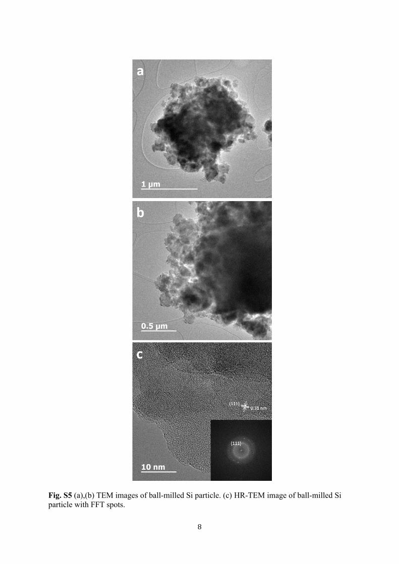
Fig. S5 (a),(b) TEM images of ball-milled Si particle. (c) HR-TEM image of ball-milled Si particle with FFT spots.
9
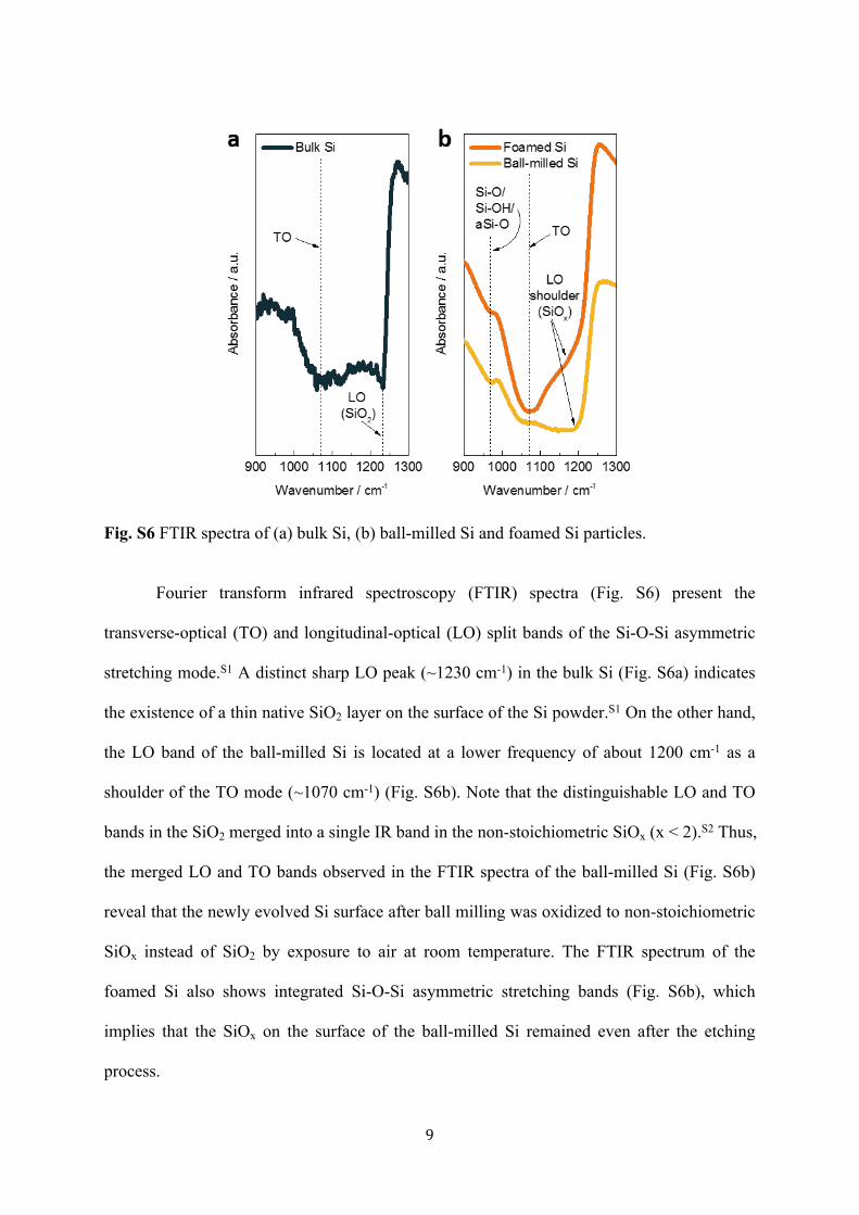
Fig. S6 FTIR spectra of (a) bulk Si, (b) ball-milled Si and foamed Si particles.
Fourier transform infrared spectroscopy (FTIR) spectra (Fig. S6) present the
transverse-optical (TO) and longitudinal-optical (LO) split bands of the Si-O-Si asymmetric
stretching mode.S1 A distinct sharp LO peak (~1230 cm-1) in the bulk Si (Fig. S6a) indicates
the existence of a thin native SiO2 layer on the surface of the Si powder.S1 On the other hand,
the LO band of the ball-milled Si is located at a lower frequency of about 1200 cm-1 as a
shoulder of the TO mode (~1070 cm-1) (Fig. S6b). Note that the distinguishable LO and TO
bands in the SiO2 merged into a single IR band in the non-stoichiometric SiOx (x < 2).S2 Thus,
the merged LO and TO bands observed in the FTIR spectra of the ball-milled Si (Fig. S6b)
reveal that the newly evolved Si surface after ball milling was oxidized to non-stoichiometric
SiOx instead of SiO2 by exposure to air at room temperature. The FTIR spectrum of the
foamed Si also shows integrated Si-O-Si asymmetric stretching bands (Fig. S6b), which
implies that the SiOx on the surface of the ball-milled Si remained even after the etching
process.

10
Fig. S7 Cross-sectional SEM images of the foamed Si electrode after aging (left) and 1 cycle (right).
Fig. S7 shows the cross-sectional SEM images of the foamed Si electrode before and
after cycling. Compared with the aged electrode (left image of Fig. S7) for 24 h in the
electrolyte, the cycled electrode (right image of Fig. S7) had slightly thicker active material
layer. The thickness of aged and cycled electrodes were about 9.5 and 12 μm, respectively.
Note that the initial reversible areal and specific volumetric discharge capacities were about
1.32 mAh cm-2 and 1390 mAh cm-3, respectively. The foamed Si electrode showed high
integrity of active materials against huge volume changes of Si during cycling, which might
be due to the interconnected submicron sized Si network that prevents detachment of active
Si parts. Although the structure integrity of foamed Si electrode was stable (Fig. S7), the
foamed Si electrode showed a gradual decrease of discharge capacity with the increase of
cycles (Fig. 4d). This might be due to the continuous solid electrolyte interphase (SEI) film
formation on the newly exposed Si surface after charge and discharge process, increasing the
impedance of the electrode.S3

11
Fig. S8 EDS mapping of a cycled foamed Si particle.

12
Table S1. BET and BJH data of bulk Si, ball-milled Si and foamed Si particles. Bulk Si Ball-milled Si Foamed Si
BET surface area
[m2 g-1]0.8173 14.6345 23.3675
BJH Adsorption
cumulative volume
of pores between
17.000 Å and
3,000.000 Å diameter
[cm3 g-1]
- 0.082548 0.133413
BJH Desorption
cumulative volume
of pores between
17.000 Å and
3,000.000 Å diameter
[cm3 g-1]
- 0.083695 0.134641
BJH Adsorption
average pore
diameter [nm]
- 39.4422 45.2832
BJH Desorption
average pore
diameter [nm]
- 29.8677 38.3226

13
Table S2. Ratios of XRD peak intensities with respect to (111) peak intensity for bulk, ball-milled and foamed Si particles.
(111)/(111) (220)/(111) (311)/(111) (400)/(111) (331)/(111) (422)/(111)
Bulk Si 1 0.58 0.29 0.06 0.11 0.14
Ball-
milled Si1 0.45 0.22 0.05 0.07 0.08
Foamed Si 1 0.52 0.29 0.07 0.1 0.12

14
Table S3. XPS data for surficial composition of bulk, ball-milled and foamed Si particles.S2p
[at%]
O1s
[at%]
Fe2p
[at%]
Na1s
[at%]
Bulk Si 53.79 46.07 0.01 0.13
Ball-milled Si 57.63 42.29 0.01 0.07
Foamed Si 52.06 47.37 0.52 0.08

15
References
S1. (a) P. Innocenzi, J. Non-Cryst. Solids, 2003, 316, 309-319; (b) K. T. Queeney, H.
Fukidome, E. E. Chaban and Y. J. Chabal, J. Phys. Chem. B, 2001, 105, 3903-3907; (c) A.
Demšar, B. Colarič, S. Rus., J. Lindav, F. Švegelj, B. Orel, B. Praček and A. Zalar, Thin
Solid Films, 1996, 281-282, 409-411.
S2. (a) P. G. Pai, S. S. Chao, Y. Takagi and G. Lucovsky, J. Vac. Sci. Technol. A, 1986, 4,
689-694; (b) C. Songyan, P. K. Kashkarov, V. Y. Timoshenko, L. Baolin and J. Bingxi, J.
Cryst. Growth, 2003, 247, 445-451; (c) K. Furukawa, Y. Liu, D. Gao, H. Nakashima, K.
Uchino and K. Muraika, Appl. Surf. Sci., 1997, 121/122, 228-232.
S3. (a) E. Radvanyi, K. V. Havenbergh, W. Porcher, S. Jouanneau, J.-S. Bridel, S. Put, S.
Franger, Electrochim. Acta, 2014, 137, 751-757; (b) J. Zheng, H. Zheng, R. Wang, L. Ben, W.
Lu, L. Chen, L. Chen and H. Li, Phys. Chem. Chem. Phys, 2014, 16, 13229-13238; (c) M.
Ashuri, Q. He and L. L. Shaw, Nanoscale, 2016, 8, 74-103; (d) Y. oumellal, N. Delpuech, D.
Mazouzi, N. Dupré, J. Gaubicher, P. Moreau, P Soudan, B. Lestriez and D. Guyomard, J.
Mater. Chem., 2011, 21, 6201-6208.


