
THE ROLE OF SINGLY-CHARGED PARTICLES IN MICROELECTRONICS
RELIABILITY
By
Brian Sierawski
Dissertation
Submitted to the Faculty of the
Graduate School of Vanderbilt University
in partial fulfillment of the requirements
for the degree of
DOCTOR OF PHILOSOPHY
in
Electrical Engineering
December, 2011
Nashville, Tennessee
Approved:
Ronald D. Schrimpf
Robert A. Reed
Marcus H. Mendenhall
Robert A. Weller
James H. Adams
c© Copyright by Brian Sierawski 2012
All Rights Reserved
ii
DEDICATION
This dissertation is dedicated to my family in appreciation of their support and
patience. To my wife Heather, thank you for your sacrifice during my academic
pursuits. Your important and sometimes unseen role in my accomplishments has
been substantial. To my children Carter and Jenna, I hope that my efforts inspire
you to use your abilities to the fullest. To my parents David and Patricia and my
brother Jeff, thank you for the beginnings of what has turned out to be a rewarding
career in electronics.

ACKNOWLEDGEMENTS
I would like to acknowledge the individuals and agencies that have made this re-
search possible. My committee members have been valuable resources in guiding the
data collection, simulation, and analysis performed in this dissertation. My cowork-
ers at the Institute for Space and Defense Electronics including Kevin Warren and
Michael Alles have also provided valuable conversations. Further, Jonathan Pellish
and Ken LaBel with the NASA Electronic Parts and Packaging Program and the
Defense Threat Reduction Agency and have provided much appreciated support to
pursue this topic. I would like to thank our corporate partners for their contributions
namely Robert Baumann at Texas Instruments, Shi-Jie Wen and Richard Wong at
Cisco Systems, and Nelson Tam at Marvell Semiconductor. Finally, Michael Trinczek
and Ewart Blackmore from TRIUMF also provided exceptional experimental support
that was essential to this research.
iv
TABLE OF CONTENTS
Page
DEDICATION . . . . . . . . . . . . . . . . . . . . . . . . . . . . . . . . . . . iii
ACKNOWLEDGEMENTS . . . . . . . . . . . . . . . . . . . . . . . . . . . . iv
LIST OF TABLES . . . . . . . . . . . . . . . . . . . . . . . . . . . . . . . . . viii
LIST OF FIGURES . . . . . . . . . . . . . . . . . . . . . . . . . . . . . . . . ix
Chapter
I. INTRODUCTION . . . . . . . . . . . . . . . . . . . . . . . . . . . . . 1
High-Reliability Applications . . . . . . . . . . . . . . . . . . . . 2Quantitative Assessment of Reliability . . . . . . . . . . . . . . . 4Requirements on Reliability . . . . . . . . . . . . . . . . . . . . . 5SEU Mechanisms . . . . . . . . . . . . . . . . . . . . . . . . . . . 6Mitigation . . . . . . . . . . . . . . . . . . . . . . . . . . . . . . . 9Background Work . . . . . . . . . . . . . . . . . . . . . . . . . . . 10
Trend in Single Event Sensitivity . . . . . . . . . . . . . . 17The Onset of Proton Direct Ionization Upsets . . . . . . . 19
Conclusions . . . . . . . . . . . . . . . . . . . . . . . . . . . . . . 21
II. PHYSICAL PROCESSES . . . . . . . . . . . . . . . . . . . . . . . . . 22
Electronic Interactions . . . . . . . . . . . . . . . . . . . . . . . . 23Electronic Stopping . . . . . . . . . . . . . . . . . . . . . . 23Electron Stripping . . . . . . . . . . . . . . . . . . . . . . 25
Range . . . . . . . . . . . . . . . . . . . . . . . . . . . . . . . . . 26Nuclear Interactions . . . . . . . . . . . . . . . . . . . . . . . . . 27
Coulomb Scattering . . . . . . . . . . . . . . . . . . . . . . 28Nuclear Elastic Scattering . . . . . . . . . . . . . . . . . . 28Nuclear Inelastic Scattering . . . . . . . . . . . . . . . . . 29Spallation . . . . . . . . . . . . . . . . . . . . . . . . . . . 29Pion Production . . . . . . . . . . . . . . . . . . . . . . . . 29Capture . . . . . . . . . . . . . . . . . . . . . . . . . . . . 30
Decay . . . . . . . . . . . . . . . . . . . . . . . . . . . . . . . . . 30Pion Decay . . . . . . . . . . . . . . . . . . . . . . . . . . 30Muon Decay . . . . . . . . . . . . . . . . . . . . . . . . . . 31
Conclusions . . . . . . . . . . . . . . . . . . . . . . . . . . . . . . 31
v
III. RADIATION ENVIRONMENTS . . . . . . . . . . . . . . . . . . . . . 33
Extraterrestrial Environments . . . . . . . . . . . . . . . . . . . . 34Interplanetary Space . . . . . . . . . . . . . . . . . . . . . 34Near Earth . . . . . . . . . . . . . . . . . . . . . . . . . . 36
Terrestrial Environments . . . . . . . . . . . . . . . . . . . . . . . 40Neutron Component . . . . . . . . . . . . . . . . . . . . . 43Proton Component . . . . . . . . . . . . . . . . . . . . . . 43Muon Component . . . . . . . . . . . . . . . . . . . . . . . 44
Conclusions . . . . . . . . . . . . . . . . . . . . . . . . . . . . . . 46
IV. ACCELERATED TESTING . . . . . . . . . . . . . . . . . . . . . . . . 48
Devices Under Test . . . . . . . . . . . . . . . . . . . . . . . . . . 50Heavy Ion Accelerated Tests . . . . . . . . . . . . . . . . . . . . . 51
Accelerated Test Setup . . . . . . . . . . . . . . . . . . . . 51Accelerated Test Results . . . . . . . . . . . . . . . . . . . 52
Proton Accelerated Testing . . . . . . . . . . . . . . . . . . . . . 55Accelerated Test Setup . . . . . . . . . . . . . . . . . . . . 55Accelerated Test Results . . . . . . . . . . . . . . . . . . . 56
Muon Accelerated Testing . . . . . . . . . . . . . . . . . . . . . . 61Accelerated Test Setup . . . . . . . . . . . . . . . . . . . . 61Experimental Validation . . . . . . . . . . . . . . . . . . . 64Accelerated Test Results . . . . . . . . . . . . . . . . . . . 66Effect of technology . . . . . . . . . . . . . . . . . . . . . . 69
Hardness Assurance Methods . . . . . . . . . . . . . . . . . . . . 72Recommendations . . . . . . . . . . . . . . . . . . . . . . . 72Low-Energy Proton Testing with a Cyclotron . . . . . . . . 77
Conclusions . . . . . . . . . . . . . . . . . . . . . . . . . . . . . . 79
V. RATE PREDICTION ANALYSES . . . . . . . . . . . . . . . . . . . . 82
Traditional Approaches . . . . . . . . . . . . . . . . . . . . . . . . 82TCAD and SPICE Analysis . . . . . . . . . . . . . . . . . . . . . 83Radiation Transport Modeling . . . . . . . . . . . . . . . . . . . . 86Single Event Upset Predictions . . . . . . . . . . . . . . . . . . . 91
Proton Response . . . . . . . . . . . . . . . . . . . . . . . 91Rate Predictions . . . . . . . . . . . . . . . . . . . . . . . 93
Conclusions . . . . . . . . . . . . . . . . . . . . . . . . . . . . . . 97
VI. IMPLICATIONS FOR FUTURE DEVICES . . . . . . . . . . . . . . . 99
Charge Collection Models . . . . . . . . . . . . . . . . . . . . . . 102On-Orbit Single Event Upsets . . . . . . . . . . . . . . . . 104Terrestrial Single Event Upsets . . . . . . . . . . . . . . . 107
Conclusions . . . . . . . . . . . . . . . . . . . . . . . . . . . . . . 112
vi
VII. CONCLUSIONS . . . . . . . . . . . . . . . . . . . . . . . . . . . . . . 113
APPENDIX A: EXPACS GENERATED FLUX SPECTRA . . . . . . . . . . 116
REFERENCES . . . . . . . . . . . . . . . . . . . . . . . . . . . . . . . . . . 126
vii
LIST OF TABLES
Table Page
1. Physical properties for singly-charged particles . . . . . . . . . . . . . . 23
2. Coulomb Barrier Potentials for Common Semiconductor Materials . . . 29
3. Device Under Test . . . . . . . . . . . . . . . . . . . . . . . . . . . . . 50
4. Baseline error counts characterized versus bias for 65 nm SRAM . . . . 51
5. Texas Instruments 65 nm Experimental Ion Species and Energies . . . . 52
6. Texas Instruments 45 nm Experimental Ion Species and Energies . . . . 52
7. Facilities Offering Muon Sources . . . . . . . . . . . . . . . . . . . . . . 61
8. Single event upset counts for 65 nm SRAM . . . . . . . . . . . . . . . . 70
9. Critical Charge Estimates . . . . . . . . . . . . . . . . . . . . . . . . . 86
10. Positive Muon Flux at Sea Level in NYC . . . . . . . . . . . . . . . . . 116
11. Negative Muon Flux at Sea Level in NYC . . . . . . . . . . . . . . . . 118
12. Proton Flux at Sea Level in NYC . . . . . . . . . . . . . . . . . . . . . 120
13. Neutron Flux at Sea Level in NYC . . . . . . . . . . . . . . . . . . . . 122
viii
LIST OF FIGURES
Figure Page
1. Circuit level schematic diagram of a six transistor SRAM . . . . . . . . 7
2. Cross sectional device level view of an inverter . . . . . . . . . . . . . . 7
3. RC equivalent model used to explain a single event transient . . . . . . 8
4. Estimated error rates for devices . . . . . . . . . . . . . . . . . . . . . . 12
5. The differential flux of cosmic rays transported through 10 cm of concrete 13
6. Prediction of device upset rates . . . . . . . . . . . . . . . . . . . . . . 14
7. Critical charge trend with technology scaling . . . . . . . . . . . . . . . 18
8. The trend in SRAM single bit SER as a function of technology node . . 19
9. Single event upset counts for low-energy protons . . . . . . . . . . . . . 20
10. Mass stopping power for protons, pions, muons, and positrons in Si . . 25
11. Range in Si for protons, pions, muons, and positrons . . . . . . . . . . 27
12. The Near-Earth Interplanetary particle flux spectra during solar minimum 35
13. The Near-Earth Interplanetary particle flux spectra during solar maximum 36
14. The Near-Earth Interplanetary particle flux spectra during the worst dayscenario . . . . . . . . . . . . . . . . . . . . . . . . . . . . . . . . . . . 37
15. AP8MIN omnidirectional proton flux with energy ≥ 0.1 MeV . . . . . . 39
16. The International Space Station particle flux spectra . . . . . . . . . . 39
17. Illustration of cosmic ray interactions in the atmosphere generating show-ers of daughter particles . . . . . . . . . . . . . . . . . . . . . . . . . . 41
18. Sea level environment . . . . . . . . . . . . . . . . . . . . . . . . . . . . 42
19. Correlation between the solar activity and counts reported by the ClimaxNeutron Monitor and Nagoya Muon Station [69]. . . . . . . . . . . . . 44
20. Differential proton momentum spectrum at sea level . . . . . . . . . . . 45
21. Differential muon momentum spectrum at sea level . . . . . . . . . . . 45
ix
22. The rate of stopping muons measured at various depth underground . . 47
23. Heavy ion single event upset cross sections for the Texas Instruments65 nm SRAM measured at LBNL and TAMU. . . . . . . . . . . . . . . 53
24. Heavy ion single event upset cross sections for the Texas Instruments45 nm SRAM measured at LBNL. . . . . . . . . . . . . . . . . . . . . . 54
25. The low-energy proton spectrum at the Lawrence Berkeley National Lab-orator . . . . . . . . . . . . . . . . . . . . . . . . . . . . . . . . . . . . 57
26. Simulated kinetic energy spectra . . . . . . . . . . . . . . . . . . . . . . 58
27. Texas Instruments 65 nm SRAM in the beam line at Lawrence BerkeleyNational Laboratories . . . . . . . . . . . . . . . . . . . . . . . . . . . . 58
28. Proton single event upset cross-section curve for the Texas Instruments65 nm SRAM . . . . . . . . . . . . . . . . . . . . . . . . . . . . . . . . 60
29. Proton single event upset cross-section curve for the Texas Instruments45 nm SRAM . . . . . . . . . . . . . . . . . . . . . . . . . . . . . . . . 60
30. The surface muon momentum produced by the M20B beamline at TRIUMF 62
31. The M20 beam line at TRIUMF . . . . . . . . . . . . . . . . . . . . . . 63
32. The Texas Instruments 65 nm SRAM in the M20B beamline at TRIUMF 64
33. The surface barrier detector in the M20B beamline at TRIUMF . . . . 65
34. Experimental and simulated energy deposition counts in surface barrierdetector . . . . . . . . . . . . . . . . . . . . . . . . . . . . . . . . . . . 66
35. Simulated muon kinetic energy distributions and measured error countsfor 65 nm, 45 nm, and 40 nm SRAMs . . . . . . . . . . . . . . . . . . . 68
36. Error counts for 65 nm SRAM versus supply voltage . . . . . . . . . . 69
37. Experimental muon-induced single event upset probability for each de-vice under test operated at nominal supply voltage . . . . . . . . . . . 71
38. A comparison of experimental and calculated mass stopping power forhydrogen on silicon. . . . . . . . . . . . . . . . . . . . . . . . . . . . . . 73
39. Simulated kinetic energy spectra of a 65 MeV proton beam after degrading 78
40. Prediction of measured proton SEU cross sections using various de-graders in a 65 MeV beam . . . . . . . . . . . . . . . . . . . . . . . . . 80
41. TCAD model of a 65 nm bulk CMOS SRAM . . . . . . . . . . . . . . . 84
x
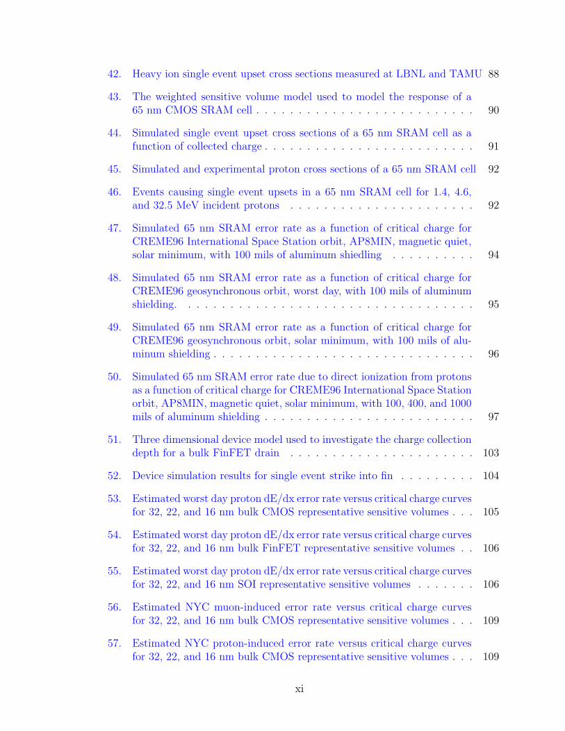
42. Heavy ion single event upset cross sections measured at LBNL and TAMU 88
43. The weighted sensitive volume model used to model the response of a65 nm CMOS SRAM cell . . . . . . . . . . . . . . . . . . . . . . . . . . 90
44. Simulated single event upset cross sections of a 65 nm SRAM cell as afunction of collected charge . . . . . . . . . . . . . . . . . . . . . . . . . 91
45. Simulated and experimental proton cross sections of a 65 nm SRAM cell 92
46. Events causing single event upsets in a 65 nm SRAM cell for 1.4, 4.6,and 32.5 MeV incident protons . . . . . . . . . . . . . . . . . . . . . . 92
47. Simulated 65 nm SRAM error rate as a function of critical charge forCREME96 International Space Station orbit, AP8MIN, magnetic quiet,solar minimum, with 100 mils of aluminum shiedling . . . . . . . . . . 94
48. Simulated 65 nm SRAM error rate as a function of critical charge forCREME96 geosynchronous orbit, worst day, with 100 mils of aluminumshielding. . . . . . . . . . . . . . . . . . . . . . . . . . . . . . . . . . . 95
49. Simulated 65 nm SRAM error rate as a function of critical charge forCREME96 geosynchronous orbit, solar minimum, with 100 mils of alu-minum shielding . . . . . . . . . . . . . . . . . . . . . . . . . . . . . . . 96
50. Simulated 65 nm SRAM error rate due to direct ionization from protonsas a function of critical charge for CREME96 International Space Stationorbit, AP8MIN, magnetic quiet, solar minimum, with 100, 400, and 1000mils of aluminum shielding . . . . . . . . . . . . . . . . . . . . . . . . . 97
51. Three dimensional device model used to investigate the charge collectiondepth for a bulk FinFET drain . . . . . . . . . . . . . . . . . . . . . . 103
52. Device simulation results for single event strike into fin . . . . . . . . . 104
53. Estimated worst day proton dE/dx error rate versus critical charge curvesfor 32, 22, and 16 nm bulk CMOS representative sensitive volumes . . . 105
54. Estimated worst day proton dE/dx error rate versus critical charge curvesfor 32, 22, and 16 nm bulk FinFET representative sensitive volumes . . 106
55. Estimated worst day proton dE/dx error rate versus critical charge curvesfor 32, 22, and 16 nm SOI representative sensitive volumes . . . . . . . 106
56. Estimated NYC muon-induced error rate versus critical charge curvesfor 32, 22, and 16 nm bulk CMOS representative sensitive volumes . . . 109
57. Estimated NYC proton-induced error rate versus critical charge curvesfor 32, 22, and 16 nm bulk CMOS representative sensitive volumes . . . 109
xi

58. Estimated NYC muon-induced error rate versus critical charge curvesfor 32, 22, and 16 nm bulk FinFET representative sensitive volumes . . 110
59. Estimated NYC proton-induced error rate versus critical charge curvesfor 32, 22, and 16 nm bulk FinFET representative sensitive volumes . . 110
60. Estimated NYC muon-induced error rate versus critical charge curvesfor 32, 22, and 16 nm SOI representative sensitive volumes . . . . . . . 111
61. Estimated NYC proton-induced error rate versus critical charge curvesfor 32, 22, and 16 nm SOI representative sensitive volumes . . . . . . . 111
xii

CHAPTER I
INTRODUCTION
In this dissertation, I propose that the emergence of direct-ionization induced sin-
gle event upsets from singly-charged particles will significantly contribute to the error
rate of deep-submicron microelectronics operating in nearly all environments. The im-
plication of this susceptibility will be an additional source of errors in microelectronics
along with those currently anticipated by rate prediction methods. The objective of
this work is to advance the methods and models to address this mechanism.
In the remainder of Chapter I the issues of reliability, single event effects, and pre-
vious published works are discussed. The history of microelectronics susceptibility to
ionizing radiation is recounted beginning with the predictions by reliability pioneers
that singly-charged particles would one day represent an insurmountable obstacle to
continued progress in the fabrication of microelectronics. Chapter II addresses mat-
ters of energy loss from ionizing radiation specifically focusing on the processes that
are of relevance to single event effects. Chapter III reviews the radiation environments
in which microelectronics are deployed. Chapter IV details the experimental proce-
dures performed and results obtained that demonstrate ionization in semiconductor
materials from a singly-charged particle, namely a proton or muon, can cause errors
in memories. By extension, these events will also be capable of producing effects
in other types of sequential circuits and logic. Experimental results are used to de-
velop a model for single event upset in Chapter V. The implications of this increased
sensitivity inherently introduced by improvements in fabrication and lithography are
1
examined in Chapter VI.
As a result of these data and analyses, it is recommended that future high-
reliability microelectronics be evaluated for their susceptibility to erroneous oper-
ation from singly-charged particles. Such an undertaking will require experience with
these mechanisms and support from proton facilities. In addition, the development of
methods will be required to advise on matters of testing. To complete the analyses,
suitable models or procedures must be proposed to evaluate a part’s use in space or
on Earth based on results obtained in accelerated environments.
High-Reliability Applications
The reliability of microelectronics such as memories, controllers, etc. is a pri-
mary concern for terrestrial and space applications. The natural ionizing radiation
environment poses a significant threat to the operation of these devices. The inter-
actions of ionizing radiation with the materials constituting a solid state device can
cause parametric shifts in operation, destructive failures, or transient errors. Under
the umbrella of radiation effects, the interaction of individual radiation quanta with
electronics is termed single event effects (SEE). These are events which result in the
transient or catastrophic failure of a solid-state device. One effect, termed a sin-
gle event upset (SEU) occurs as the result of radiation-induced charge carriers that
cause a sequential circuit to change data state. Single event effects on-orbit have been
attributed to heavy ions and proton-induced nuclear reaction events. In terrestrial
environments, neutrons and alpha emitting contaminants have been associated with
errors. In particular, static random access memories (SRAMs), registers, latches, and
flip-flops are all vulnerable to SEU. Following an upset the altered circuit’s state may
2
be propagated, but not necessarily recognized, as an erroneous data or control value.
High-reliability applications place stringent requirements on the frequency of SEU.
These requirements are often motivated by acceptable levels of risk and the cost
of operating in an otherwise unprotected manner. Modern devices have increased
packing density and speed, decreased power dissipation and capacitance, and are
more cost effective than previous generations. The same trends in device scaling that
these applications leverage are the cause of increased susceptibility to upset.
Satellites and exploration vehicles, costing hundreds of millions of dollars each,
are exposed to a wide range of ionizing particle species and energies in space. Certain
systems such as data collection may permit the occasional corruption of data; how-
ever, errors in critical systems such as control could result in mission failure. These
high budget missions have the luxury of funding and using radiation tolerant devices
when required. Even so, commercial-off-the-shelf (COTS) electronics are appealing
to designers as an avenue to reduce mass, volume, power, and ultimately the cost
of launching and operating the satellite. However, Bendel and Petersen, both well
known individuals in the radiation effects, community once made the forward-looking
statement that
A device sensitive to the ionization in a proton track would be grossly unfit
for spacecraft use.[1]
Suborbital aviation systems use COTS parts more heavily than their orbiting
counterparts. Because of cost, the aerospace industry faces the challenge of selecting
parts that have been designed for other applications and still ensuring reliable op-
eration. Historically, avionic design has ignored SEE and assumed that the level of
3
fault tolerance built into the system will prevent calamity. However, recent reports
of in-flight anomalies in avionics have captured the attention of the industry.
Computing servers, routers, and communication systems provide the backbone for
commerce and other critical systems to modern society. The proliferation of these
systems and the increased reliance placed on them underscores our need for them
to operate correctly. Expectations for these commodity parts to work flawlessly put
pressure on designing resilient systems. It is therefore important to understand and
anticipate the SEU mechanisms and to have the capability to test for these effects in
a manner that yields accurate predictions of the field failure rate.
Quantitative Assessment of Reliability
One metric of reliability is the frequency at which a part will fail. For many
systems this is expressed as the mean time between failures (MTBF). Reliability can
also be expressed as the inverse of MTBF, the number of failures in a specified time
period. The particular unit of reporting varies with the community.
For space-bound parts, the error rates are typically expressed as the number of
upsets per bit per day in memories, or more generally as upsets per device per day.
This may also be calculated on shorter time periods to evaluate the instantaneous
error rate observed when encountering periods of high particle flux.
The terrestrial semiconductor community has adopted the unit of FIT (Failures
in Time) or failures per 1 billion hours of operation. Memory devices are often
normalized to their (Mbit) capacity. This is colloquially referred to as the soft error
rate.
These values are only valid under the associated operating conditions and radiation
4
environment. A useful relationship to bridge the two communities is:
1 FIT/Mbit = 2.4× 10⁻¹⁴ upsets/bit/day (1)
Requirements on Reliability
As part of NASA’s single event effects criticality analysis (SEECA) on spacecraft,
different parts of the craft have different reliability requirements according to the risk
presented to the mission. In [2], LaBel et al. make the following recommendation for
space-faring vehicles that are using commercial off-the-shelf (COTS) components.
“Wherever practical, procure SEU immune devices. In devices which are
not SEU-immune, the improper operation caused by an SEU must be re-
duced to acceptable levels, and may not cause performance anomalies or
outages which require ground intervention to correct. Additionally, analy-
sis for SEU rates and effects must take place based on the experimentally
determined LET th and σ of the candidate; if such device test data does
not exist, ground testing is required.”
LaBel et al. also note in [3] that while the test documents such as the JEDEC
standards [4, 5] are good guidelines, the increase in device complexity has introduced
new phenomena and traditional approaches to testing must be updated to reflect this.
Further, as of yet, there are no such guidelines for proton or muon testing.
The International Technology Roadmap for Semiconductors (ITRS) is a forward
looking assessment of the direction of the fabrication process with emphasis on iden-
tifying challenges and establishing requirements [6]. The reliability requirements are
5
implicitly provided for terrestrial environments. In reports prior to the 2009 edi-
tion, the SRAM soft error rate requirement was indicated as 1000-2000 FIT/Mbit
(although 2006 and prior years were not properly normalized by capacity). The 2009
edition inexplicably increases the error rate to 11,000 FIT/Mbit. The relevant value,
of course, is ultimately determined by the application.
SEU Mechanisms
A single event upset occurs as the result of carrier generation near an active region
of a sequential circuit. The mechanisms of energy deposition and charge generation
will be covered in Chapter II, whereas this chapter discusses the circuit effects. Al-
though upsets can occur in any type of sequential circuit, the following descriptions of
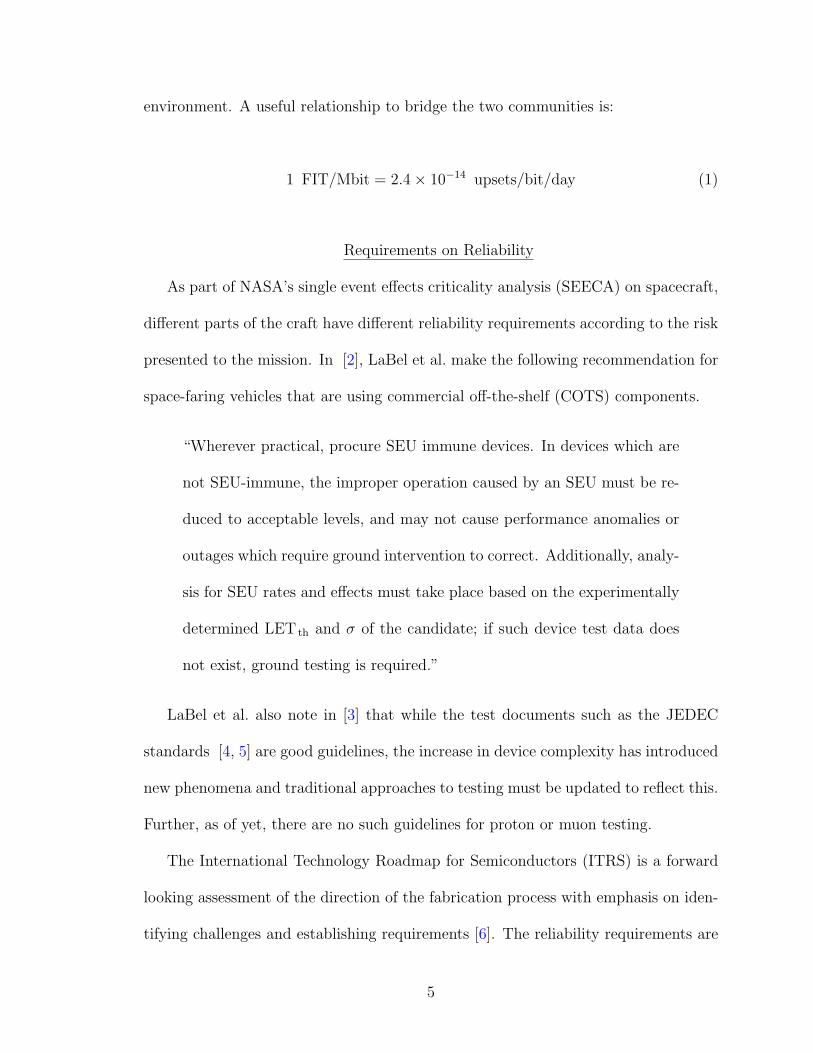
the mechanism will be discussed for an SRAM cell without any loss of generality. The
six transistor (6T) SRAM cell is one of the most basic sequential circuits. Figure 1
captures the basic design. The cell stores a logic value in a feedback loop maintained
by a pair of coupled inverters. These four transistors, M1, M2, M3, and M4, act to
reinforce a stable logic state. When the cell is storing a 0, M1 and M4 are both off.
For reasons explained at the device level, this makes their drain diffusions sensitive
to upset. In practice, the access transistors M5 and M6 are also both off while the
cell is holding data but typically are designed as a shared diffusion with the adjacent
NMOS device.
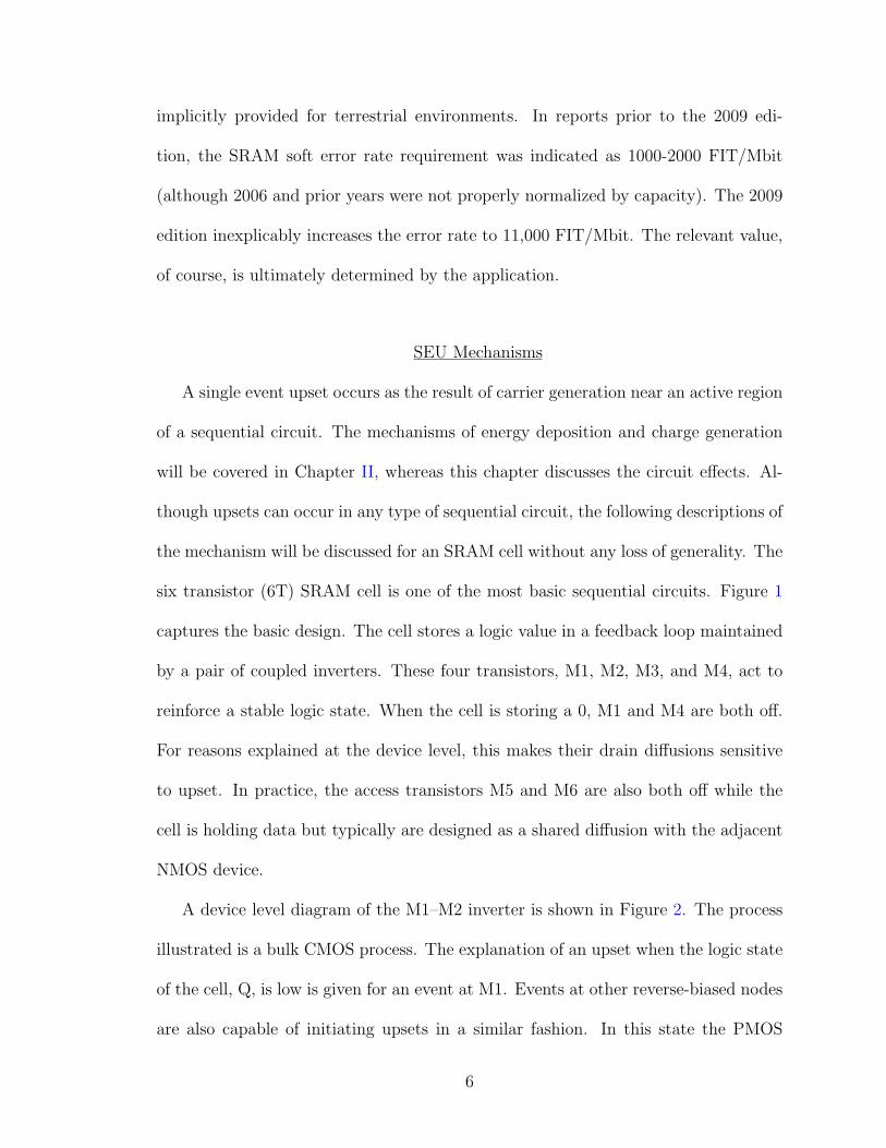
A device level diagram of the M1–M2 inverter is shown in Figure 2. The process
illustrated is a bulk CMOS process. The explanation of an upset when the logic state
of the cell, Q, is low is given for an event at M1. Events at other reverse-biased nodes
are also capable of initiating upsets in a similar fashion. In this state the PMOS
6
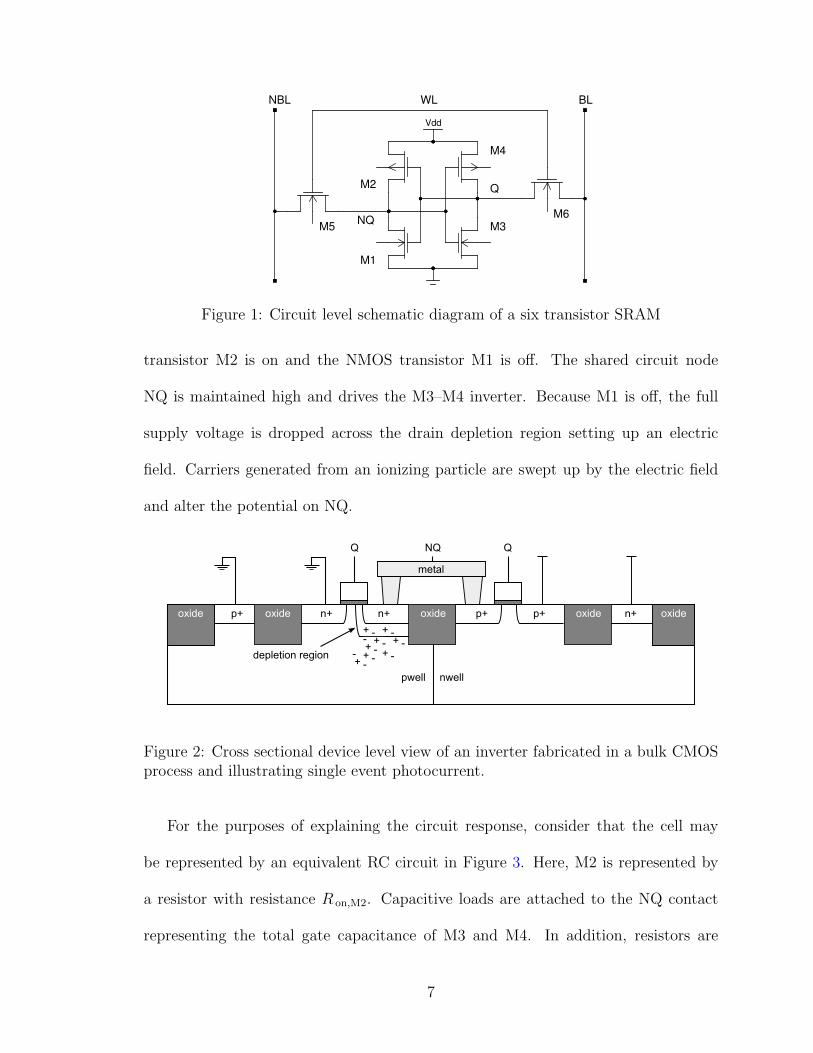
Figure 1: Circuit level schematic diagram of a six transistor SRAM
transistor M2 is on and the NMOS transistor M1 is off. The shared circuit node
NQ is maintained high and drives the M3–M4 inverter. Because M1 is off, the full
supply voltage is dropped across the drain depletion region setting up an electric
field. Carriers generated from an ionizing particle are swept up by the electric field
and alter the potential on NQ.
Figure 2: Cross sectional device level view of an inverter fabricated in a bulk CMOSprocess and illustrating single event photocurrent.
For the purposes of explaining the circuit response, consider that the cell may
be represented by an equivalent RC circuit in Figure 3. Here, M2 is represented by
a resistor with resistance R on,M2. Capacitive loads are attached to the NQ contact
representing the total gate capacitance of M3 and M4. In addition, resistors are
7
placed at appropriate locations to represent the resistance to a contact through the
well.
Cg,M4
Cg,M3Rpwell
Rnwell
Ron,M2
ISEU
NQ
Rpwell
Vdd Vdd
+ −
−+
Figure 3: RC equivalent model used to explain a single event transient in the M1–M2inverter of an SRAM.
To first order, the charge carriers generated by the single event may be represented
as an independent current source ISEU at M1. As current flows through the M1 drain-
to-body junction, an equal current must flow into the drain from M2 and the M3 and
M4 gates. Initially, charge is stored on the M3 gate capacitor. During the event,
the capacitor will discharge and the M4 gate capacitor will charge. The amount of
current that the capacitors can supply to NQ (at that instantaneous voltage) dictates
the current required to flow through M2. This current creates a potential drop across
M2. Therefore the capacitive loads help to maintain the state of the cell.
If the photocurrent at M1 is sufficiently high and maintained for a long enough
time, the capacitors will not be able to hold the potential at NQ and it will drop to
ground. When this begins to happen, the M3–M4 inverter will switch. The cell then
enters a stable, but errant, state with Q high and NQ low.
Once the charge generated by the event recombines or is swept away, the current
source will shut off. If the circuit has not yet flipped, either because the amount
8
of charge was insufficient to do so or the feedback time in the circuit is too long
compared to the event, the potentials will be restored and the cell will return to the
correct data state.
Mitigation
A number of techniques are available to mitigate SEUs; from altering the local
radiation environment to modifying the circuit design, but each have associated draw-
backs. For applications required to use COTS parts, modification of the circuit or
creating a custom design is not an option.
In the simplest case, shielding surrounding the device can reduce the energy and
flux of incident particles. Although the device sensitivity does not change, the fre-
quency of SEU-inducing particles in the local environment arriving at the active
electronics may be reduced and the error rate improved proportionally. It is also pos-
sible that the shielding may make the local environment worst by contributing to the
low-energy portion of the spectra. This solution has the obvious drawback that heavy
shielding may be required to make any significant difference in the local environment
seen by the part. Particularly for space missions, adding otherwise unnecessary mass
is an undesirable proposition.
Radiation-hardened-by-design techniques can be used to decrease the sensitivity
of a cell to ionizing radiation through redundant elements in a circuit or the use
of structures designed to minimize charge collection. Similarly, redundancy at the
system, architecture, or logical level can be effective at filtering errors in one portion
of the design. These techniques necessarily have area and power costs that have
prevented them from being used on a wide scale.
9

For certain portions of an integrated chip, such as an SRAM, error correcting
codes (ECC) are often used to detect and correct errors within a data word. These
codes are effective against occasional single bit errors but cannot easily be used for
sparse sequential elements such as latches and flip-flops. The extra circuitry also
introduces delay into read accesses.
Often a combination of well-selected techniques is needed to protect an integrated
circuit against errors. Mitigation will reduce, but cannot eliminate the possibility of
radiation-induced errors.
Background Work
In 1962, three years before the now infamous prediction by Gordon Moore regard-
ing the yearly industry growth in the number of components in an integrated function,
one of the first doomsday predictions on microelectronics scaling was published by
Wallmark and Marcus [7]. This publication made the case that scaling in the fledgling
industry would soon cease because of fundamental physical limitations. In additional
to photolithographic resolution, excess heat generation, and fluctuations in doping
concentration, the authors cited cosmic rays as one of the fundamental phenomena to
limit the minimum size of integrated circuits. The analysis considered the hard and
soft components of the terrestrial environment, specifically pointing out what were
then known as µ-mesons. Just like the many predictions that would follow in the
footsteps [8], the limits to Moore’s law have not yet come to pass and the industry
has far exceeded both predictions of minimum feature size and reliability.
The argument was that the flux of cosmic rays passing through an arbitrary cube
was so great that a computer with 105 components each 10 µm3 would suffer a mean
10
time to failure of one month (107 FIT/Mbit). The calculation, performed for only
two classes, lightly and highly ionizing particles, assumed that any terrestrial cosmic
ray particle passing through a cell was sufficient to cause a soft error. Although in
hindsight, the limits were premature, the fundamental arguments are applicable and
soft errors from cosmic rays are still a threat to reliability.
A little over ten years later, evidence of single event effects began to appear. The
first report to implicate ionizing radiation as the source of anomalous errors came in
1975. In this report, Binder et al. attributed the frequency of failures to the event
rate of impinging iron ions on one of 40 JK flip-flops used on-board a communications
satellite [9]. In 1978, May and Woods identified alpha emissions from uranium and
thorium contaminants in packaging materials as a source for soft errors [10].
Shortly after the initial reports, Ziegler and Lanford published a thorough survey
on the terrestrial particle environment and interactions that lead to charge generation
in semiconductors [11]. In the analysis, burst-generation curves are used to evaluate
the frequency of particle events of a given energy. The analysis of the relative con-
tribution to the error rate for selected parts includes the effects due to electrons,
muons, protons, and neutrons through consideration of the ionization wake, recoil,
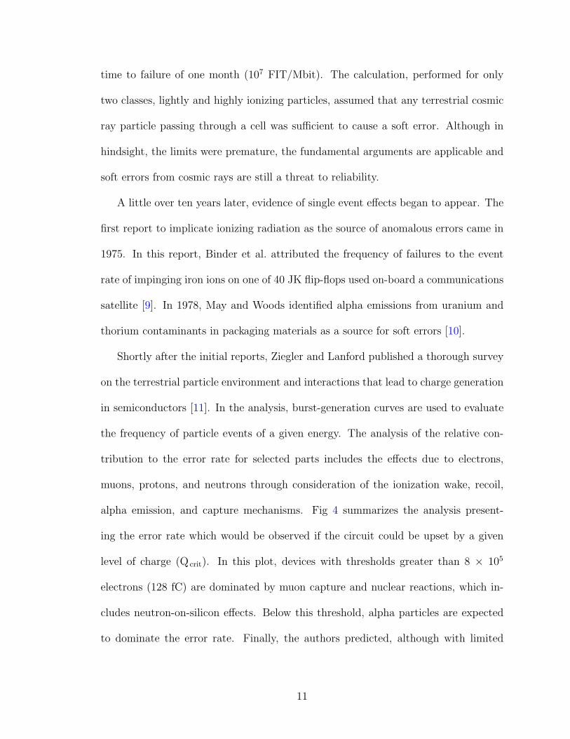
alpha emission, and capture mechanisms. Fig 4 summarizes the analysis present-
ing the error rate which would be observed if the circuit could be upset by a given
level of charge (Q crit). In this plot, devices with thresholds greater than 8 × 10⁵
electrons (128 fC) are dominated by muon capture and nuclear reactions, which in-
cludes neutron-on-silicon effects. Below this threshold, alpha particles are expected
to dominate the error rate. Finally, the authors predicted, although with limited
11
environmental measurements, that CCDs and future devices with extremely low crit-
ical charge values (< 16 fC), would be susceptible to upset from the muon ionization
wake. This susceptibility would increase the error rate by orders of magnitude.
The thresholds are not general, but are specific to the device geometry assumed in
this analysis. Over the years of technology scaling, devices have been subject to upset
from neutron-induced nuclear reactions and alpha particles have grown to become a
large concern as well. A sensitivity to muons never materialized in the single event
effects literature. This is in part due to the changing dimensions of microelectronics
and the dominance of the other mechanisms. The works of [7] and [11] established a
warning however, that muons could have a tremendously negative effect on reliability.
103
104
105
106
107
Qcrit
(Number of Electrons)
10-1
100
101
102
103
Err
or
Rate
Per
Ch
ip (
Err
ors
/Mh
r)
Muon IonizationThreshold(10 Electrons)
Alpha-ParticleIonizationThreshold(8x10 Electrons)
Nuclear Reactions
Muon Capture
5
5
Figure 4: Estimated error rates for devices with critical charge values related to thethreshold for different mechanisms of charge generation. Reproduced from [11].
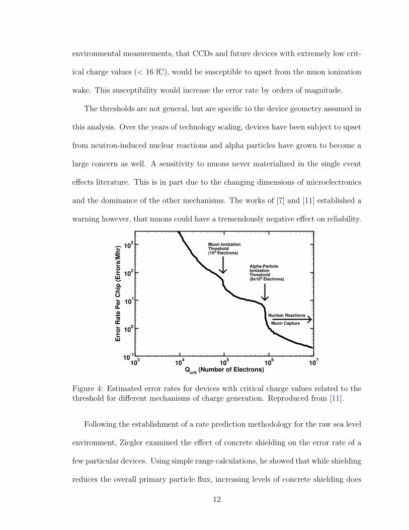
Following the establishment of a rate prediction methodology for the raw sea level
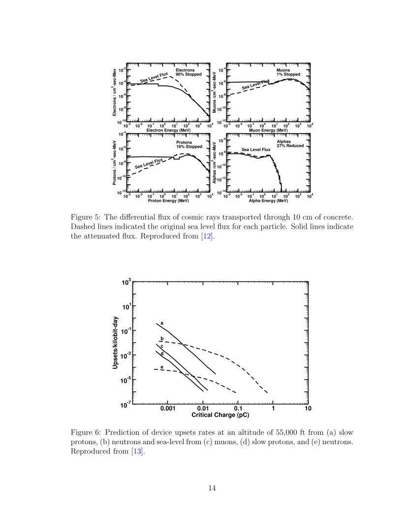
environment, Ziegler examined the effect of concrete shielding on the error rate of a
few particular devices. Using simple range calculations, he showed that while shielding
reduces the overall primary particle flux, increasing levels of concrete shielding does
12
not guarantee a decreased particle flux over the entire energy range [12]. In particular,
the electromagnetic force will shift the energy distribution of charged particles to lower
energy because of interactions with electrons in the shielding. The nuclear force will
stop some of the hadrons and ions in the shielding, producing secondary particles in
the process. This effect will act on neutrons, protons, and ions, but not muons. The
final result is that high-energy particles are slowed down and additional particles may
be produced. Ignoring secondary particle cascades, the particle fluxes under 10 cm of
concrete are shown in Figure 5. Ziegler expected the muon capture and distributed
charge burst rate to increase beneath one meter of concrete. The muon component
in these calculations was estimated to be 99.8% of the entire particle flux. It was
determined that ten meters of concrete were needed to attenuate the muon flux. In
a final analysis of the failure rate of a dynamic memory, it was concluded that parts
with a high critical charge will see a decrease in error rate due to shielding, but for
sensitive parts, the error rate will increase.
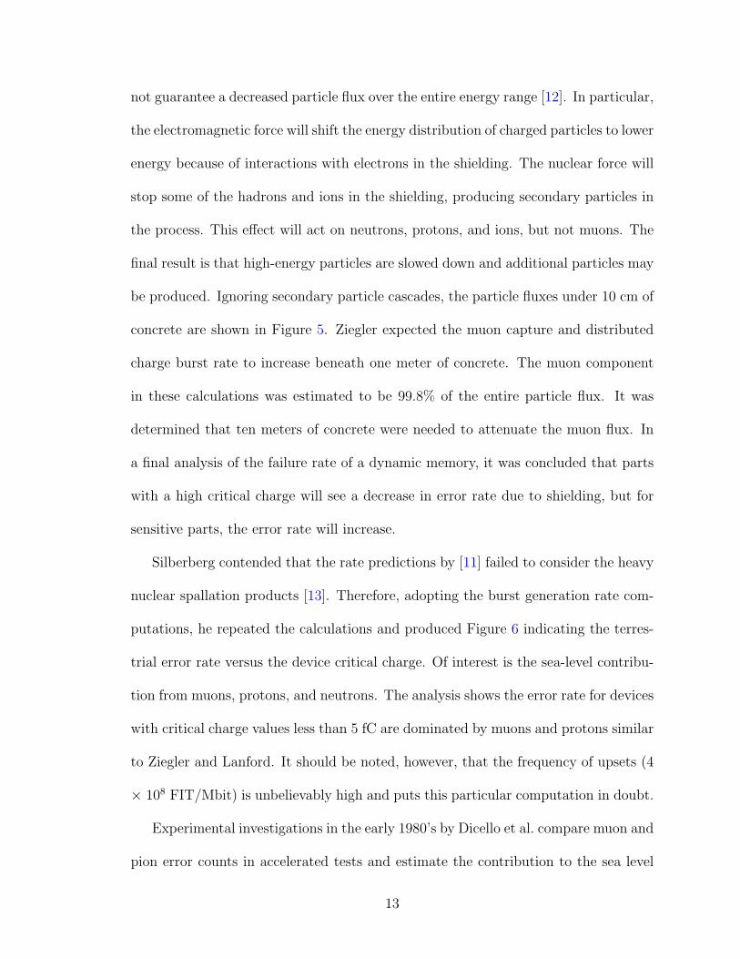
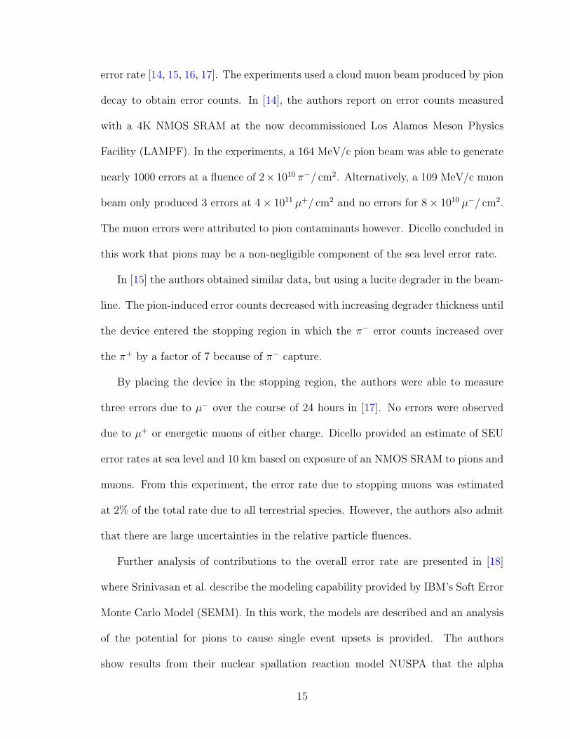
Silberberg contended that the rate predictions by [11] failed to consider the heavy
nuclear spallation products [13]. Therefore, adopting the burst generation rate com-
putations, he repeated the calculations and produced Figure 6 indicating the terres-
trial error rate versus the device critical charge. Of interest is the sea-level contribu-
tion from muons, protons, and neutrons. The analysis shows the error rate for devices
with critical charge values less than 5 fC are dominated by muons and protons similar
to Ziegler and Lanford. It should be noted, however, that the frequency of upsets (4
× 108 FIT/Mbit) is unbelievably high and puts this particular computation in doubt.
Experimental investigations in the early 1980’s by Dicello et al. compare muon and
pion error counts in accelerated tests and estimate the contribution to the sea level
13
10-3
10-2
10-1
100
101
102
103
104
Electron Energy (MeV)
10-10
10-8
10-6
10-4
10-2
Ele
ctr
on
s /
cm
2-s
ec
-Me
v
10-3
10-2
10-1
100
101
102
103
104
Muon Energy (MeV)
10-12
10-10
10-8
10-6
10-4
Mu
on
s /
cm
2-s
ec
-Me
V
10-3
10-2
10-1
100
101
102
103
104
Proton Energy (MeV)
10-12
10-10
10-8
10-6
10-4
Pro
ton
s /
cm
2-s
ec
-Me
V
10-3
10-2
10-1
100
101
102
103
104
Alpha Energy (MeV)
10-14
10-12
10-10
10-8
10-6
Alp
ha
s /
cm
2-s
ec
-Me
V
Sea Level FluxElectrons90% Stopped
Sea Level Flux
Protons16% Stopped
Sea Level Flux
Muons1% Stopped
Sea Level Flux
Alphas27% Reduced
Figure 5: The differential flux of cosmic rays transported through 10 cm of concrete.Dashed lines indicated the original sea level flux for each particle. Solid lines indicatethe attenuated flux. Reproduced from [12].
0.001 0.01 0.1 1 10Critical Charge (pC)
10-7
10-5
10-3
10-1
101
103
Up
sets
/kilo
bit
-day
a
b
c
d
e
Figure 6: Prediction of device upsets rates at an altitude of 55,000 ft from (a) slowprotons, (b) neutrons and sea-level from (c) muons, (d) slow protons, and (e) neutrons.Reproduced from [13].
14
error rate [14, 15, 16, 17]. The experiments used a cloud muon beam produced by pion
decay to obtain error counts. In [14], the authors report on error counts measured
with a 4K NMOS SRAM at the now decommissioned Los Alamos Meson Physics
Facility (LAMPF). In the experiments, a 164 MeV/c pion beam was able to generate
nearly 1000 errors at a fluence of 2× 10¹⁰ π−/ cm2. Alternatively, a 109 MeV/c muon
beam only produced 3 errors at 4× 10¹¹ µ+/ cm2 and no errors for 8× 10¹⁰ µ−/ cm2.
The muon errors were attributed to pion contaminants however. Dicello concluded in
this work that pions may be a non-negligible component of the sea level error rate.
In [15] the authors obtained similar data, but using a lucite degrader in the beam-
line. The pion-induced error counts decreased with increasing degrader thickness until
the device entered the stopping region in which the π− error counts increased over
the π+ by a factor of 7 because of π− capture.
By placing the device in the stopping region, the authors were able to measure
three errors due to µ− over the course of 24 hours in [17]. No errors were observed
due to µ+ or energetic muons of either charge. Dicello provided an estimate of SEU
error rates at sea level and 10 km based on exposure of an NMOS SRAM to pions and
muons. From this experiment, the error rate due to stopping muons was estimated
at 2% of the total rate due to all terrestrial species. However, the authors also admit
that there are large uncertainties in the relative particle fluences.
Further analysis of contributions to the overall error rate are presented in [18]
where Srinivasan et al. describe the modeling capability provided by IBM’s Soft Error
Monte Carlo Model (SEMM). In this work, the models are described and an analysis
of the potential for pions to cause single event upsets is provided. The authors
show results from their nuclear spallation reaction model NUSPA that the alpha
15
differential production cross section from pions in silicon is greater than from protons
at 250 MeV. They also speculate that the moderately larger production cross section
may be significant for terrestrial and especially high-altitude error rates.
In [19] the SEU cross section of DRAM memories exposed to 150 MeV π− were
experimentally measured approximately 4 times greater than for protons of the same
energy. Similar results can be found in [20]. Duzellier et al. measured SEU cross
sections for π+ at 58, 147 and 237 MeV and protons for both SRAMs (0.5 to 0.8 µm
processes) and DRAMs (0.35 to 0.5 µm processes) in [21] and found that protons
were slightly more capable of causing SEU than pions. These results in both cases
suggest that pions upset devices in a similar fashion as p–Si interactions.
Tang expounded on the NUSPA software system in [22]. He concluded that the
effect from pions would be a small correction to sea level error rate predictions because
the flux is lower than the flux of neutrons, but that it should be included in any
analysis at higher altitudes. He also asserted that muons are not a concern for single
event effects. The reasoning behind this argument is that slow positive muons (<
1 MeV) will capture an electron forming muonium and result in a pair of gammas
through a decay and annihilation. These processes will be discussed in Chapter II.
Fast muons are too lightly ionizing and unable to cause SEE.
Normand demonstrated in [23] that the dominant component of the terrestrial
cosmic ray environment causing SEU was high-energy neutrons. The correlation of
measured chip failure rates with measurements made at the Los Alamos Weapons
Neutron Research Facility essentially put to rest the debate over the dominant source
of errors.
Ziegler and Puchner write that pion capture is well-known through geological
16
analysis and occurs at a rate of 8.5/cm3-year [24]. The subsequent fission event may
release up to 22 nC. For a given chip volume of 3× 10⁻⁵ cm3, and the large quantity
of charge generated, pion capture contributes roughly 30 FIT even behind a couple
of feet of concrete. Pions also interact through the strong force and the authors point
out that in Leadville, CO, the proton and pion flux are sufficiently high that they
must be considered in addition to neutrons.
Muons do not interact through the strong force so they can penetrate much farther
through shielding. Muon capture rarely cause charge generation. In these rare cases
the event could be a silicon recoil or emission of an alpha in total contributing to
70 FIT.
Duzellier et al. further studied the energy threshold for proton-induced SEU in [25].
The study examined a number of memories and showed the SEU cross section versus
proton energy for each. The data set shows that while most parts have an energy
threshold between 10 and 20 MeV, some were lower. The authors concluded that
effects from electronic stopping were not evident, but could be if thresholds continued
to decrease below 2 MeV.
Trend in Single Event Sensitivity
Measured critical charge thresholds have been shown to decrease steadily with
technology scaling. In [26, 27], Petersen et al. presented a collection of critical charge
(Q crit) values for memories fabricated in various processes and feature sizes. As one
would expect, the thresholds for upset is smaller according to feature size. Applying
a least squares curve fit using a power law, the data can be used to extrapolate onset
charge to smaller feature sizes. The data imply that moving to the next technology
17
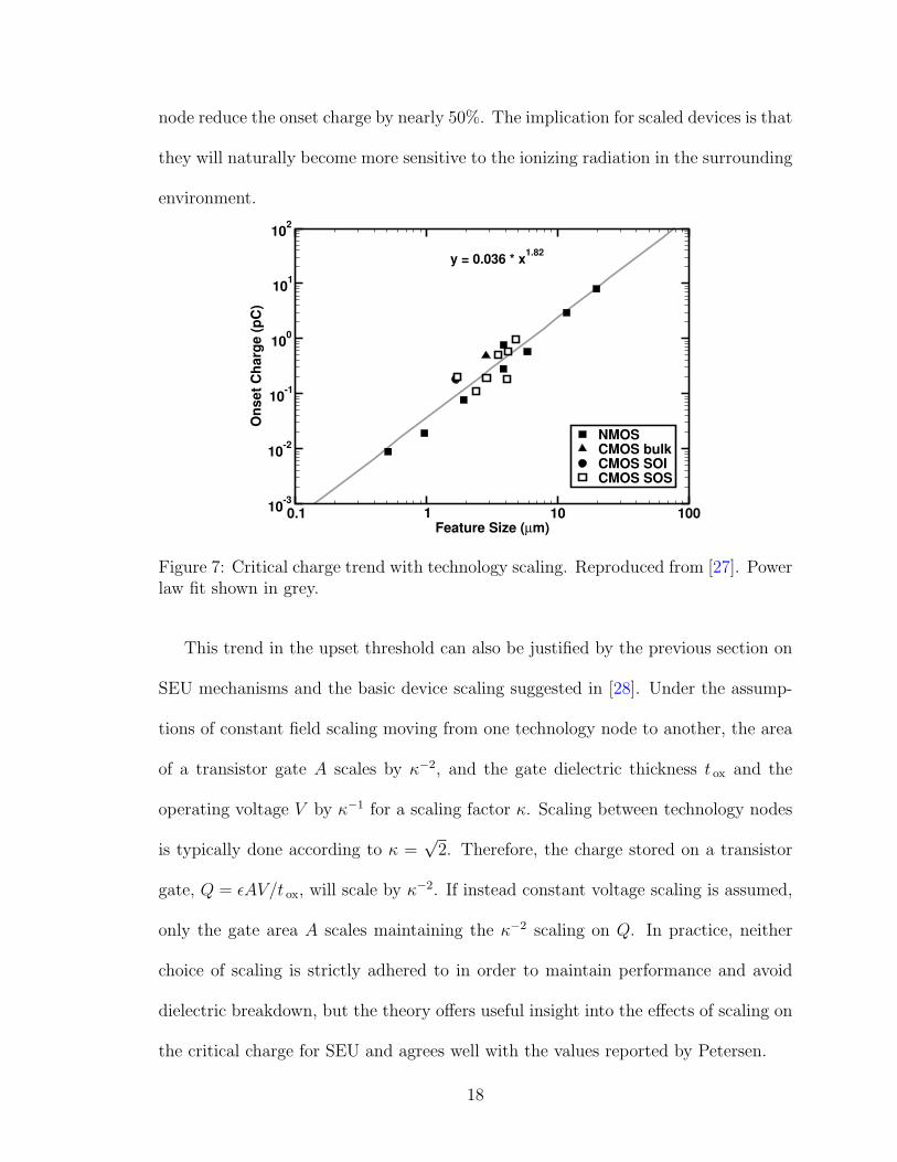
node reduce the onset charge by nearly 50%. The implication for scaled devices is that
they will naturally become more sensitive to the ionizing radiation in the surrounding
environment.
0.1 1 10 100Feature Size (µm)
10-3
10-2
10-1
100
101
102
On
set
Ch
arg
e (
pC
)
NMOSCMOS bulkCMOS SOICMOS SOS
y = 0.036 * x1.82
Figure 7: Critical charge trend with technology scaling. Reproduced from [27]. Powerlaw fit shown in grey.
This trend in the upset threshold can also be justified by the previous section on
SEU mechanisms and the basic device scaling suggested in [28]. Under the assump-
tions of constant field scaling moving from one technology node to another, the area
of a transistor gate A scales by κ−2, and the gate dielectric thickness t ox and the
operating voltage V by κ−1 for a scaling factor κ. Scaling between technology nodes
is typically done according to κ =√
2. Therefore, the charge stored on a transistor
gate, Q = εAV/t ox, will scale by κ−2. If instead constant voltage scaling is assumed,
only the gate area A scales maintaining the κ−2 scaling on Q. In practice, neither
choice of scaling is strictly adhered to in order to maintain performance and avoid
dielectric breakdown, but the theory offers useful insight into the effects of scaling on
the critical charge for SEU and agrees well with the values reported by Petersen.
18
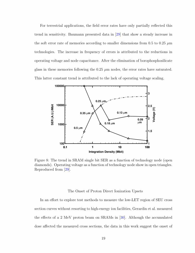
For terrestrial applications, the field error rates have only partially reflected this
trend in sensitivity. Baumann presented data in [29] that show a steady increase in
the soft error rate of memories according to smaller dimensions from 0.5 to 0.25 µm
technologies. The increase in frequency of errors is attributed to the reductions in
operating voltage and node capacitance. After the elimination of borophosphosilicate
glass in these memories following the 0.25 µm nodes, the error rates have saturated.
This latter constant trend is attributed to the lack of operating voltage scaling.
0.1 1 10 100
Integration Density (Mbit)
100
1000
10000
100000
SE
R (
A.U
.)/M
bit
0.1 1 10 100
1
1.5
2
2.5
3
Vo
ltag
e (
V)
0.5 µm
0.35 µm
0.25 µm
0.13 µm
0.18 µm
0.09µm
Figure 8: The trend in SRAM single bit SER as a function of technology node (opendiamonds). Operating voltage as a function of technology node show in open triangles.Reproduced from [29].
The Onset of Proton Direct Ionization Upsets
In an effort to explore test methods to measure the low-LET region of SEU cross
section curves without resorting to high-energy ion facilities, Gerardin et al. measured
the effects of a 2 MeV proton beam on SRAMs in [30]. Although the accumulated
dose affected the measured cross sections, the data in this work suggest the onset of
19

proton direct ionization induced SEU in these technologies.
Heidel et al. later presented a model for determining the critical charge for latches
and memory in [31]. By varying the angle of incidence of a monochromatic alpha
beam, the sensitivity of various circuit designs fabricated in an IBM 65 nm SOI tech-
nology were determined and used to calculate the charge required for upset through
geometric arguments. Estimates of the critical charge ranged from 0.5 to 1.0 fC.
The method presented by Heidel and the aforementioned report [30] prompted a
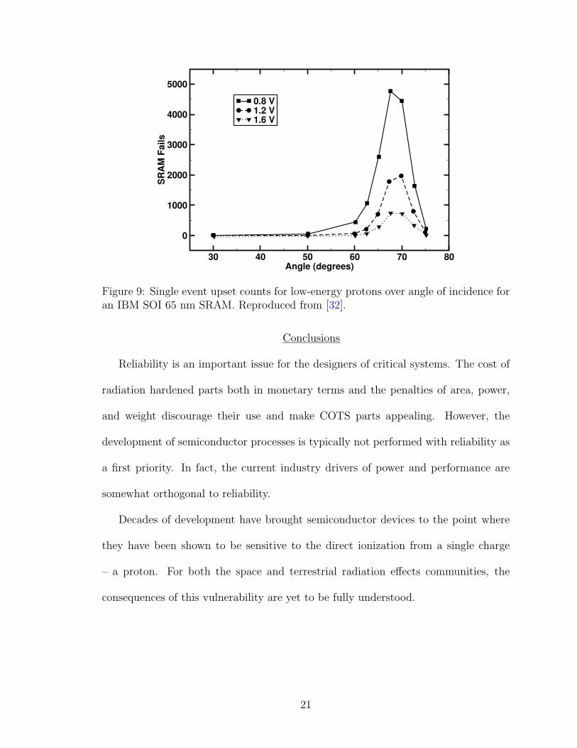
test of the same IBM parts with a low-energy proton beam by Rodbell et al. [32].
These data, shown in Figure 9, demonstrate the increase in SRAM fails as the part
is rotated in a proton beam. The errors at angle are the result of charge generated
from the proton’s extended path length through the device which exceed the critical
charge. These data are now regarded as the first conclusive evidence of proton direct
ionization induced SEU. The impact for on-orbit applications was later estimated
in [33] by studying the ratio of the low-energy and high-energy proton environment
and respective SEU cross sections.
Kobayashi et al. extended the impact of proton direct ionization from space to the
terrestrial environment [34]. PHITS simulations indicate that terrestrial error rates
will increase with technology scaling because low energy protons are secondaries from
n–Si reactions. Although the general error rate trend with scaling decreases in this
analysis, the proton sensitivity is predicted to cause the rate in sub 45 nm SRAMs
to increase.
20
30 40 50 60 70 80Angle (degrees)
0
1000
2000
3000
4000
5000
SR
AM
Fa
ils
0.8 V1.2 V1.6 V
Figure 9: Single event upset counts for low-energy protons over angle of incidence foran IBM SOI 65 nm SRAM. Reproduced from [32].
Conclusions
Reliability is an important issue for the designers of critical systems. The cost of
radiation hardened parts both in monetary terms and the penalties of area, power,
and weight discourage their use and make COTS parts appealing. However, the
development of semiconductor processes is typically not performed with reliability as
a first priority. In fact, the current industry drivers of power and performance are
somewhat orthogonal to reliability.
Decades of development have brought semiconductor devices to the point where
they have been shown to be sensitive to the direct ionization from a single charge
– a proton. For both the space and terrestrial radiation effects communities, the
consequences of this vulnerability are yet to be fully understood.
21
CHAPTER II
PHYSICAL PROCESSES
Radiation can generate charge in semiconductor devices through a variety of mech-
anisms. Energetic particles lose energy through interactions with matter and the na-
ture of the interaction determines both the amount and spatial distribution of the
energy. The particles considered in this section and their physical properties are pre-
sented in Table 1. The table does not represent an exhaustive list of singly-charged
particles in the Standard Model, but only those with a mean lifetime greater than
1 ns. It is reasonable to believe that shorter lived particles will have virtually no
impact on devices.
The interactions of these particles may be through electronic and nuclear stop-
ping, elastic and inelastic nuclear scattering, Coulomb scattering, spallation, or cap-
ture. Further, unstable particles undergo decay. These processes are discussed in this
section with an emphasis on energy deposition relevant for single particle induced
transient behaviors. Each of these processes must be understood to accurately assess
the radiation response of microelectronics in arbitrary radiation environments. The
effects of accumulated dose and damage events are addressed elsewhere in literature
and will not be recounted here.
The stopping power of a medium is the mean rate of energy loss (−dE/dx) by an
energetic particle through the material. The stopping power can be subdivided into
electronic and nuclear components as the loss of kinetic energy is due to the Coulombic
interactions with electrons and nuclei. For energetic particles the electronic stopping
22
power is substantially greater than the nuclear stopping power. These rates of energy
loss are commonly normalized to the density of the medium and expressed in units
of MeV-cm2/mg. The interactions are described in more detail here.
Table 1: Physical properties for singly-charged particles
Symbol Particle Mass (MeV/c2) Mean Lifetime
e electron / positron 0.510 998 910(13) –µ muon 105.658 367(4) 2.2 µsπ pion 139.570 18(35) 26 nsK kaon 493.667 12 nsp proton 938.272 013(23) –
Electronic Interactions
Electronic Stopping
The electronic stopping power arises from a particle’s energy loss due to inelastic
collisions with electrons in the target medium through the electromagnetic force. A
portion of the energy loss will result in valence electrons being raised to an excited
state in the conduction band. These electrons (and holes) contribute to the ion-
induced photocurrent. High energy transfers to electrons provide kinetic energy to
the electrons, resulting in delta rays that may distribute the energy away from the
ion track and create additional electron-hole pairs. The maximum amount of energy
transferred to an electron is denoted by Tmax.
The mean rate of energy loss, is described by the Bethe-Bloch equation. The
form in Equation 2 is the first order Born approximation [35]. The formula contains
terms for the electron charge e, mass of an electron me, speed of light c, the relative
particle velocity β, and the particle charge unit z. K, Z, A, and I are properties
23
of the target medium. Details of the origins and higher-level corrections can also be
found in [36, 37]. When including the corrections it is believed to accurately describe
the stopping power for protons down to 1 MeV.
− dE
dx= Kz2Z
A
1
β2
[1
2ln
2mec2β2γ2Tmax
I2− β2 − δ(βγ)
2
](2)
From Equation 2 it can be observed that the energy loss in a given material
depends heavily on the charge of the incident particle. Therefore all singly-charged
particles will have approximately the same rate of energy loss at the same velocity β.
For single event effects, these curves are typically parameterized over kinetic energy.
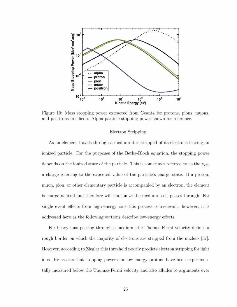
As the particle slows in the Bethe-Bloch region, the mass stopping power increases
as shown in Figure 10. This continues until the stopping power reaches a maximum
at low energy known as the Bragg peak. For protons, the Bragg Peak occurs at
approximately 50 keV, depositing a little over 0.5 MeV-cm2/mg. Charged pions and
muons reach the Bragg Peak at approximately 8 keV. Experimental data [38, 39, 40]
have confirmed and refined these stopping power curves.
The mass stopping power curves for µ−, π−, and e− are not shown in Figure 10.
The curves follow the general shape of their antiparticle, but have slightly lower values
of stopping power as described by the Barkas effect [35].
The ionizing energy lost to the target medium produces electron-hole pairs in
semiconductors. For silicon this ionization energy has been empirically measured at
3.6 eV. From this value a convenient conversion for silicon is 22.5 MeV of ionizing
energy deposition yields 1 pC of charge.
24
102
103
104
105
106
107
Kinetic Energy (eV)
10-3
10-2
10-1
100
Mass S
top
pin
g P
ow
er
(MeV
-cm
2/m
g)
alphaproton
pionmuonpositron
Figure 10: Mass stopping power extracted from Geant4 for protons, pions, muons,and positrons in silicon. Alpha particle stopping power shown for reference.
Electron Stripping
As an element travels through a medium it is stripped of its electrons leaving an
ionized particle. For the purposes of the Bethe-Bloch equation, the stopping power
depends on the ionized state of the particle. This is sometimes referred to as the z eff ,
a charge referring to the expected value of the particle’s charge state. If a proton,
muon, pion, or other elementary particle is accompanied by an electron, the element
is charge neutral and therefore will not ionize the medium as it passes through. For
single event effects from high-energy ions this process is irrelevant, however, it is
addressed here as the following sections describe low-energy effects.
For heavy ions passing through a medium, the Thomas-Fermi velocity defines a
rough border on which the majority of electrons are stripped from the nucleus [37].
However, according to Ziegler this threshold poorly predicts electron stripping for light
ions. He asserts that stopping powers for low-energy protons have been experimen-
tally measured below the Thomas-Fermi velocity and also alludes to arguments over
25
whether energetic protons could ever capture an electron due to the size of the elec-
tron’s orbital diameter. If some of the protons are not stripped at these low-energies,
then the refinements to the theory based on measurements of stopping power already
reflect this. He argues that the Bethe-Bloch equation is being used outside of its
validity in this regime anyhow. Therefore the stopping power of a single particle may
be slightly larger than these models predict but it is unlikely that a large percentage
have captured an electron.
A similar occurrence happens for muons. When an electron orbits a slow µ+
particle, it creates a short-lived element similar to hydrogen known as muonium.
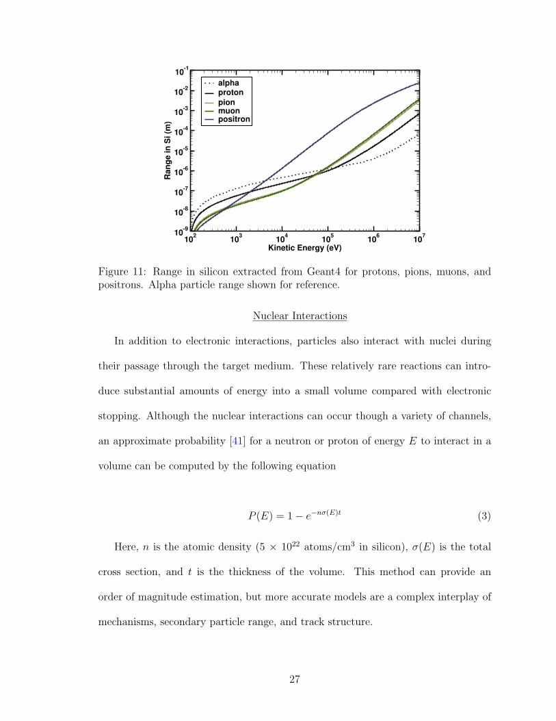
Range
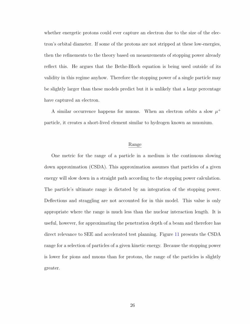
One metric for the range of a particle in a medium is the continuous slowing
down approximation (CSDA). This approximation assumes that particles of a given
energy will slow down in a straight path according to the stopping power calculation.
The particle’s ultimate range is dictated by an integration of the stopping power.
Deflections and straggling are not accounted for in this model. This value is only
appropriate where the range is much less than the nuclear interaction length. It is
useful, however, for approximating the penetration depth of a beam and therefore has
direct relevance to SEE and accelerated test planning. Figure 11 presents the CSDA
range for a selection of particles of a given kinetic energy. Because the stopping power
is lower for pions and muons than for protons, the range of the particles is slightly
greater.
26
102
103
104
105
106
107
Kinetic Energy (eV)
10-9
10-8
10-7
10-6
10-5
10-4
10-3
10-2
10-1
Ra
ng
e i
n S
i (m
)
alphaproton
pionmuonpositron
Figure 11: Range in silicon extracted from Geant4 for protons, pions, muons, andpositrons. Alpha particle range shown for reference.
Nuclear Interactions
In addition to electronic interactions, particles also interact with nuclei during
their passage through the target medium. These relatively rare reactions can intro-
duce substantial amounts of energy into a small volume compared with electronic
stopping. Although the nuclear interactions can occur though a variety of channels,
an approximate probability [41] for a neutron or proton of energy E to interact in a
volume can be computed by the following equation
P (E) = 1− e−nσ(E)t (3)
Here, n is the atomic density (5 × 10²² atoms/cm3 in silicon), σ(E) is the total
cross section, and t is the thickness of the volume. This method can provide an
order of magnitude estimation, but more accurate models are a complex interplay of
mechanisms, secondary particle range, and track structure.
27

Coulomb Scattering
Coulomb scattering occurs when an incident particle interacts with a nucleus
in the target material through the electromagnetic force. Because kinetic energy is
conserved, this mechanism is considered an elastic scatter. When the particle interacts
with a nucleus in this manner, it may impart enough energy to break the atom free
from a semiconductor crystal lattice. In this case, the recoiling nucleus can deposit
energy as well.
Nuclear Elastic Scattering
The elastic scattering process occurs when an incident particle interacts through
the strong force with a nucleus in the target material, imparting some of the initial
energy to the nucleus, and conserving total kinetic energy. The kinetic energy im-
parted to the recoiling nucleus can be computed according to Equation 4 given the
initial particle kinetic energy Ep and mass m and the scattering angle θ (in the center
of mass frame) of the recoil with mass M .
E recoil =4mM
(m+M)2Ep cos2 θ (4)
In particular for neutrons, this process can occur for any incident kinetic energy.
According to this equation, a 10 MeV neutron, which is a relevant threshold for
electronics reliability, is capable of producing a 1.3 MeV silicon or 2.2 MeV oxygen
recoiling nucleus.
The Coulomb barrier to overcome the electromagnetic force experienced by a
charged particle is given by Equation 5 [42] and summarized for common elements in
Table 2.
28

U coul = 1.03× A1 + A2
A2
× Z1Z2
A11/3 + A2
1/3(5)
Table 2: Coulomb Barrier Potentials for Common Semiconductor MaterialsTarget Nucleus Proton Energy (MeV)
16O 2.528Si 3.7
63Cu 6.1184W 11.5
Nuclear Inelastic Scattering
The inelastic scattering process occurs when an incident particle is absorbed by a
nucleus of the target material and re-emitted with a lower kinetic energy. The process
leaves the recoiling nucleus in an excited state and therefore total kinetic energy is
not conserved. The nucleus will de-excite by emitting a gamma ray. The maximum
energy of the recoil is therefore still governed by Equation 4.
Spallation
Spallation is an inelastic event that occurs when a high-energy particle causes a
nucleus to fragment or “spall” into several parts. These reactions typically produce
several smaller fragments and often nucleons. Unlike elastic scattering where the
heavy recoiling nucleus deposits the lost energy, the small fragments can deposit
energy over a long range.
Pion Production
Pions are produced as the result of a high-energy proton-proton collision. The
energy threshold for this process is approximated by computing the incoming energy
29
of two protons in the center of mass frame, such that both stop during the collision and
135 MeV of kinetic energy is transformed into a π0. The pion production threshold
is 290 MeV in the lab frame.
Capture
Negative pions and muons can become captured by a nucleus once they have
sufficiently slowed down [43]. In this process the π− or µ− begins to orbit the nucleus
due to the Coulomb potential. Because these particles are over 200× as massive as
an electron and have spiraled down to the 1s shell, they can interact and become
captured by one of the nucleons. The process results in a large energy deposition
event often referred to as star formation.
Decay
Pion Decay
Charged pions are unstable and decay with a mean lifetime of 26 ns. Neutral
pions have a much shorter lifetime (8.4 × 10⁻¹⁷ s), only produce gammas, electrons,
and positrons, and are therefore not considered in the following sections. Charged
pions have two decay modes of which the most frequent modes (6) and (8) result
in a muon and a neutrino. Conservation of energy and momentum dictate that the
muon departs with a kinetic energy of 4.1 MeV. These decays are responsible for the
terrestrial muonic component as will be discussed in Chapter III. In the less probable
decay modes (7) and (9), the pion results in an electron and neutrino.
30
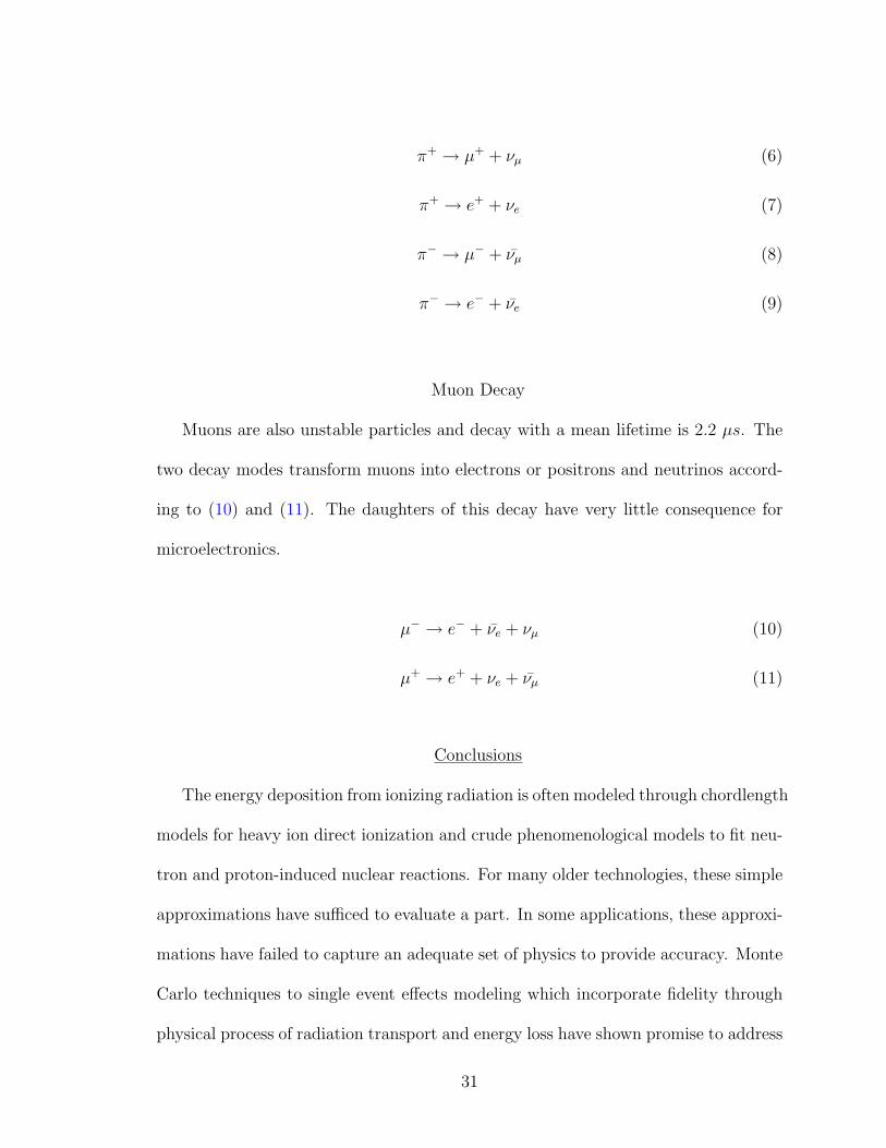
π+ → µ+ + νµ (6)
π+ → e+ + νe (7)
π− → µ− + νµ (8)
π− → e− + νe (9)
Muon Decay
Muons are also unstable particles and decay with a mean lifetime is 2.2 µs. The
two decay modes transform muons into electrons or positrons and neutrinos accord-
ing to (10) and (11). The daughters of this decay have very little consequence for
microelectronics.
µ− → e− + νe + νµ (10)
µ+ → e+ + νe + νµ (11)
Conclusions
The energy deposition from ionizing radiation is often modeled through chordlength
models for heavy ion direct ionization and crude phenomenological models to fit neu-
tron and proton-induced nuclear reactions. For many older technologies, these simple
approximations have sufficed to evaluate a part. In some applications, these approxi-
mations have failed to capture an adequate set of physics to provide accuracy. Monte
Carlo techniques to single event effects modeling which incorporate fidelity through
physical process of radiation transport and energy loss have shown promise to address
31
the shortcomings of the existing approximations. Further, an understanding of the
physical processes is important to develop test methods for singly-charged particles
and understand the results.
32

CHAPTER III
RADIATION ENVIRONMENTS
Classically, error rate predictions for devices outside the Earth’s magnetosphere
have focused on heavy ions, predictions at low Earth orbits focused on protons, and
predictions of terrestrial soft errors have considered neutrons. It is worth noting
that alpha emissions from impurities in the chip and packaging also contribute to
the overall error rate of a part. This contribution may vary wildly depending on the
purity of the processed materials. In this chapter we discuss a number of relevant
natural environments in the context of single event effects.
In the following sections which address measurements of the particle environment,
we will use the following definitions in accordance to [44]. The directional intensity
I of a particle species in a given environment is presented as I dΩ dσ dt for incident
particles over a time dt upon an area dσ, from a solid angle dΩ. The units are thus
cm−2s−1sr−1. Unless otherwise specified, these values are typically the vertical inten-
sity of the environment. Intensity measurements are a common result of telescopic
experiments and therefore a complete description, require information on the angular
distribution of the environment.
The flux J1 dσ dt measures the number of particles incident over a time dt upon
an area dσ which originate from the upper hemisphere. The units of flux are given
in cm−2s−1. It can be derived from the intensity integrated over dΩ according to
Equation 12 where θ is the extent of the solid angle from the vertical direction.
J1 =∫I cos θ dΩ (12)
33
Extraterrestrial Environments
Interplanetary Space
In the region of interstellar space outside of our sun’s heliopause particles of un-
known origins continuously stream into our solar system from all directions. These
galactic cosmic rays (GCR) consist of ionized particles that are stripped of electrons
by the stellar medium. The largest portion of the composition is hydrogen, although
most atomic elements are present. The particles have been accelerated and traveled
through the galactic magnetic field for possibly millions of years. Probes in inter-
planetary space and satellites in a geo-synchronous orbit (GEO, approx. 35,786 km
altitude) will be primarily subject to the GCR spectra. The basic form of the dif-
ferential energy spectra follows a power law of the form j1(E) ∝ E−γ where γ is
approximately 2.7 for energies between 1 GeV and 106 GeV [45]. The low-energy
portion of the spectra is modulated in local interplanetary space by the solar wind.
The cosmic ray flux is reduced during solar maximum as the solar wind resists the
interstellar particles from entering the heliopause. This wind consists of particles
emitted from the sun and therefore depends on solar activity. Both the GCRs which
penetrate the heliosphere and solar energetic particles make up the interplanetary
environment.
One popular model of the environment was proposed by Nymmik and has become
an ISO standard [46]. The algorithm simplifies the complex interactions of cosmic
ray propagation by relating the flux spectra with the Wolf (sunspot) number. In this
way, the model tends to be predictive. Other codes such as the Badhwar–O’Neill
model [47], that base the flux spectra off of correlated values from neutron monitors
34
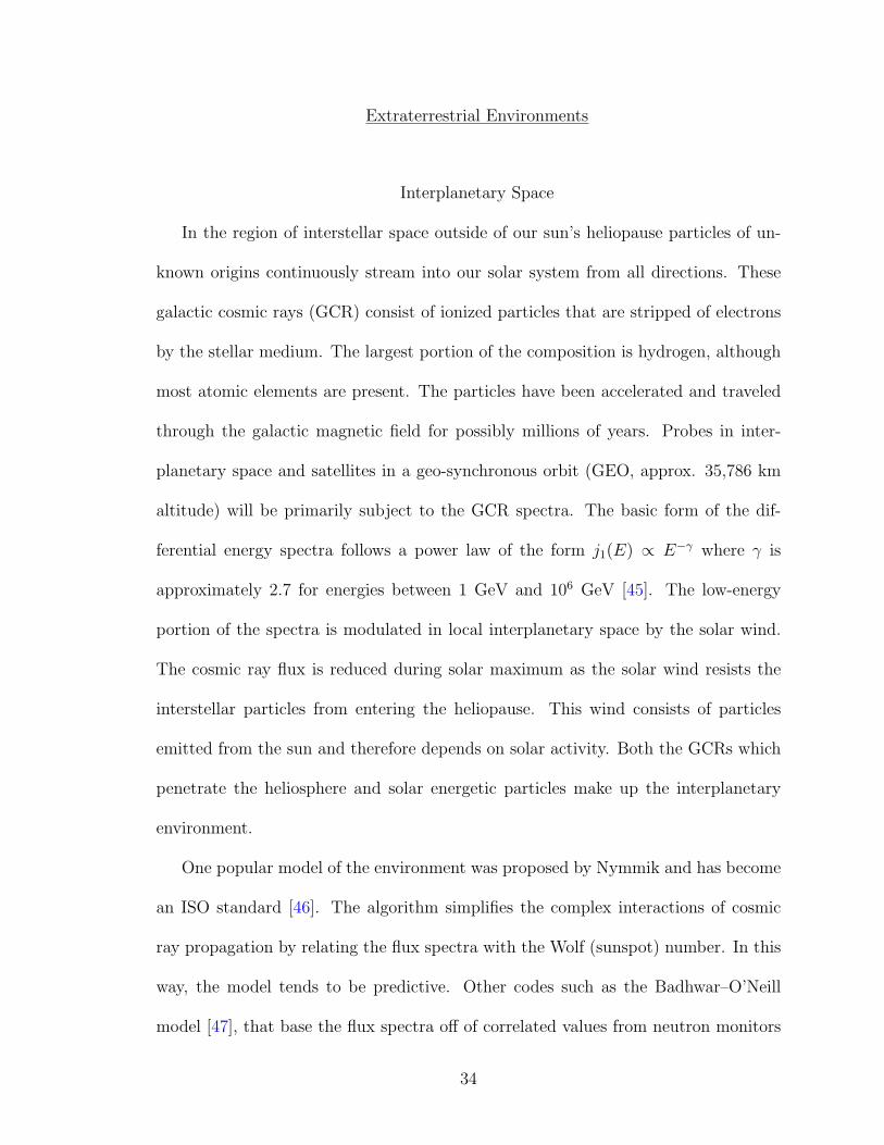
are better suited for elucidative modeling. The Cosmic Ray Effects on Microelec-
tronics (CREME96) codes [48] implement the GCR algorithm as specified in [49].
An updated version of the CREME96 GCR model conforms to the ISO draft most
notably omitting the upturn in differential flux below 10 MeV/u seen in the previous
model. Figures 12 and 13 show these spectra as computed by the original CREME96
codes. Hydrogen, the most abundant element in the universe, has the highest flux in
these environments. Helium and other light ions are typically one or more orders of
magnitude lower in flux.
100
101
102
103
104
105
Kinetic Energy (MeV/nucleon)
10-13
10-11
10-9
10-7
10-5
10-3
Flu
x (
cm
2-s
-sr-
MeV
/nu
c)-1
1-H4-He12-C14-N16-O56-Fe
Figure 12: The particle flux spectra computed by CREME96 for a Near-Earth Inter-planetary or Geosynchronous orbit during solar minimum with 100 mils of aluminumshielding. Common species shown, all others omitted.
35
100
101
102
103
104
105
Kinetic Energy (MeV/nucleon)
10-13
10-11
10-9
10-7
10-5
10-3
Flu
x (
cm
2-s
-sr-
MeV
/nu
c)-1
1-H4-He12-C14-N16-O56-Fe
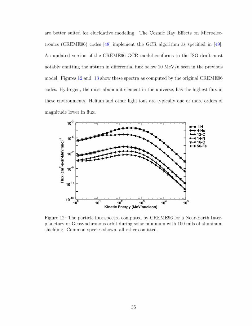
Figure 13: The particle flux spectra computed by CREME96 for a Near-Earth Inter-planetary or Geosynchronous orbit during solar maximum with 100 mils of aluminumshielding. Common species shown, all others omitted.
Near Earth
Solar Particle Events
Solar particle events are the result of coronal mass ejections from the sun’s surface.
In these events a large flux of (mostly low energy) particles are emitted into the
interplanetary medium. They follow the magnetic field lines and depending on the
position of the Earth, may arrive at the near-Earth environment. The events occur
randomly in time and vary in severity.
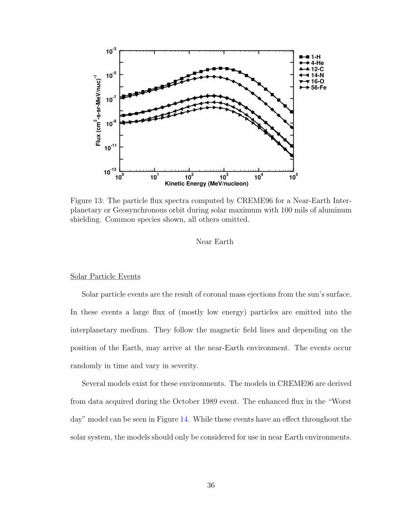
Several models exist for these environments. The models in CREME96 are derived
from data acquired during the October 1989 event. The enhanced flux in the “Worst
day” model can be seen in Figure 14. While these events have an effect throughout the
solar system, the models should only be considered for use in near Earth environments.
36

100
101
102
103
104
105
Kinetic Energy (MeV/nucleon)
10-9
10-7
10-5
10-3
10-1
101
103
Flu
x (
cm
2-s
-sr-
MeV
/nu
c)-1
1-H4-He12-C14-N16-O56-Fe
Figure 14: The particle flux spectra computed by CREME96 for a Near-Earth In-terplanetary or Geosynchronous orbit during the worst day scenario with 100 mils ofaluminum shielding. Common species shown, all others omitted.
Magnetic Rigidity
The Earth’s magnetosphere prevents low-energy charged particles from entering
the atmosphere. For low-inclination, low-Earth orbits (LEO) this is an important con-
sideration. At inclinations above 45, such as polar orbits, the geomagnetic shielding
is less effective.
Trapped Proton and Electron Belts
The Earth’s magnetic field not only prevents radiation from entering the atmo-
sphere, but also traps (relatively) low-energy particles. Van Allen is credited with
the discovery of the radiation belts. Although previously predicted, he first reported
the results of an investigation into the trapped population of particle surrounding the
Earth [50]. Using detectors on-board a satellite in 1958 with an inclination of 51 deg,
260 km perigee and 2200 km apogee, the experiment reported the counting rates as
37
a function of the satellite position. Additional investigations into the trapped popu-
lations have been carried out and have resulted in the development of environment
models with versions AP-8 and AE-8 released in 1976 [51]. Development of AP-9 and
AE-9 releases is underway to improve the accuracy of the models and address sources
of uncertainty. An excellent source of the history is recounted in [52].
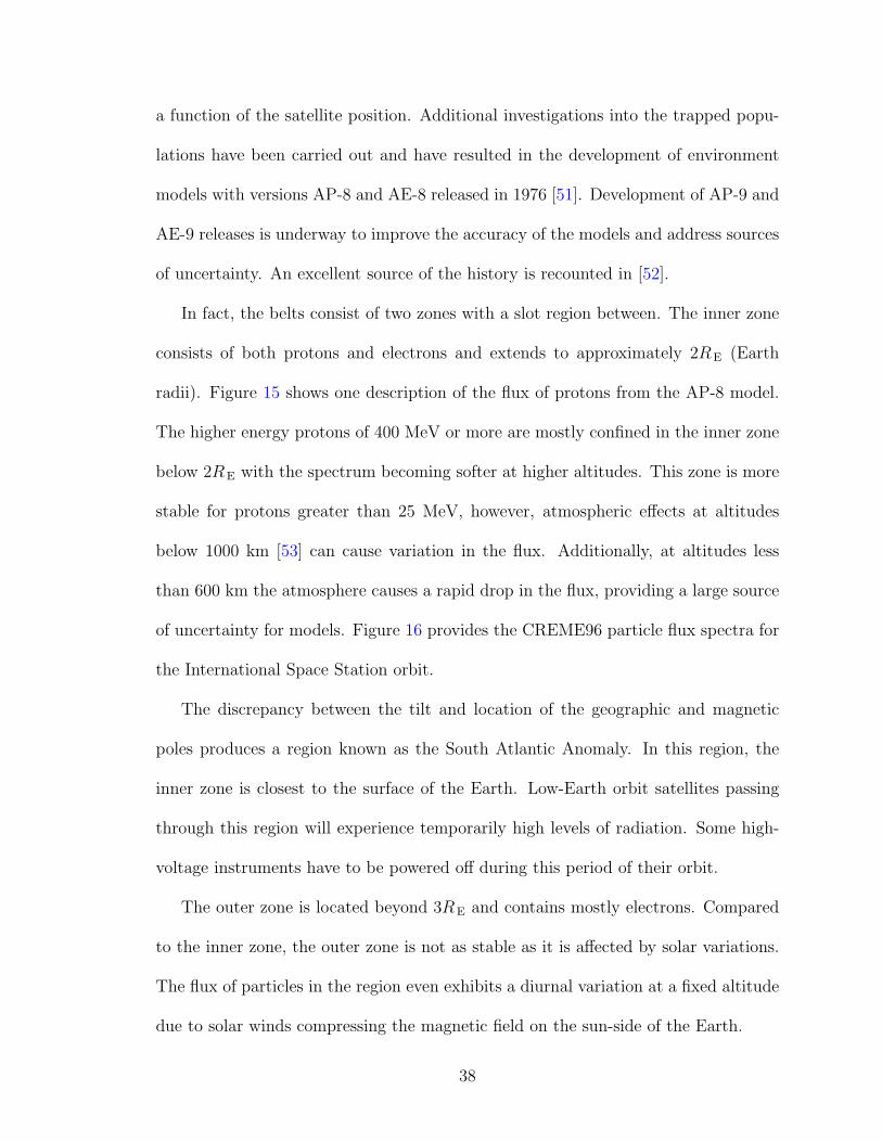
In fact, the belts consist of two zones with a slot region between. The inner zone
consists of both protons and electrons and extends to approximately 2RE (Earth
radii). Figure 15 shows one description of the flux of protons from the AP-8 model.
The higher energy protons of 400 MeV or more are mostly confined in the inner zone
below 2RE with the spectrum becoming softer at higher altitudes. This zone is more
stable for protons greater than 25 MeV, however, atmospheric effects at altitudes
below 1000 km [53] can cause variation in the flux. Additionally, at altitudes less
than 600 km the atmosphere causes a rapid drop in the flux, providing a large source
of uncertainty for models. Figure 16 provides the CREME96 particle flux spectra for
the International Space Station orbit.
The discrepancy between the tilt and location of the geographic and magnetic
poles produces a region known as the South Atlantic Anomaly. In this region, the
inner zone is closest to the surface of the Earth. Low-Earth orbit satellites passing
through this region will experience temporarily high levels of radiation. Some high-
voltage instruments have to be powered off during this period of their orbit.
The outer zone is located beyond 3RE and contains mostly electrons. Compared
to the inner zone, the outer zone is not as stable as it is affected by solar variations.
The flux of particles in the region even exhibits a diurnal variation at a fixed altitude
due to solar winds compressing the magnetic field on the sun-side of the Earth.
38

Figure 15: AP8MIN constant intensity omnidirectional flux (protons/cm2-s) withenergy ≥ 0.1 MeV. Reproduced from [51].
100
101
102
103
104
105
Kinetic Energy (MeV/nucleon)
10-13
10-11
10-9
10-7
10-5
10-3
10-1
Flu
x (
cm
2-s
-sr-
MeV
/nu
c)-1
1-H4-He12-C14-N16-O56-Fe
Figure 16: The particle flux spectra computed by CREME96 for the ISS orbit duringsolar minimum and quiet geomagnetic conditions transported through 100 mils ofaluminum shielding. Common species shown, all others omitted.
39

The slot region between the inner and outer zones is highly dependent on the
effects of solar activity on the magnetosphere, and can even become depleted. Data
have also shown that another proton belt may form just outside of the inner belt
during some solar storms and last for several months afterwards [54].
Terrestrial Environments
As high-energy GCR particles reach the Earth, they strike the atmosphere re-
sulting in nuclear reactions. At high altitudes the environment consists mainly of
protons. Several measurements of the high altitude environment have been made
[55, 56, 57, 58]. The nuclear reactions produce showers of particles in secondary and
tertiary reactions as illustrated in Figure 17. These interactions generate the “soft”
electronic, “hard” mesonic, and nucleonic components. Because of the generation of
secondary particles and the variation in atmospheric density, the intensity of particles
changes greatly with altitude. One notable region varying around 20 km in altitude
is termed the Pfotzer point [59] at which the intensity reaches a maximum.
In addition to altitude, the intensities of the atmospheric particles have distribu-
tions over zenith angle θ. It is widely accepted that this distribution can be modeled
using the vertical intensity I0 and a fitting parameter n according to Equation 13.
I = I0 cos(θ)n (13)
To complicate matters, the parameter n itself is a function of the particle energy.
Other variations in intensity exist as a result of an east-west effect, geomagnetic
rigidity, solar cycle, and diurnal variation.
To address the complications of the environments and the shortcomings of the
40

Figure 17: Illustration of cosmic ray interactions in the atmosphere generating showersof daughter particles
41
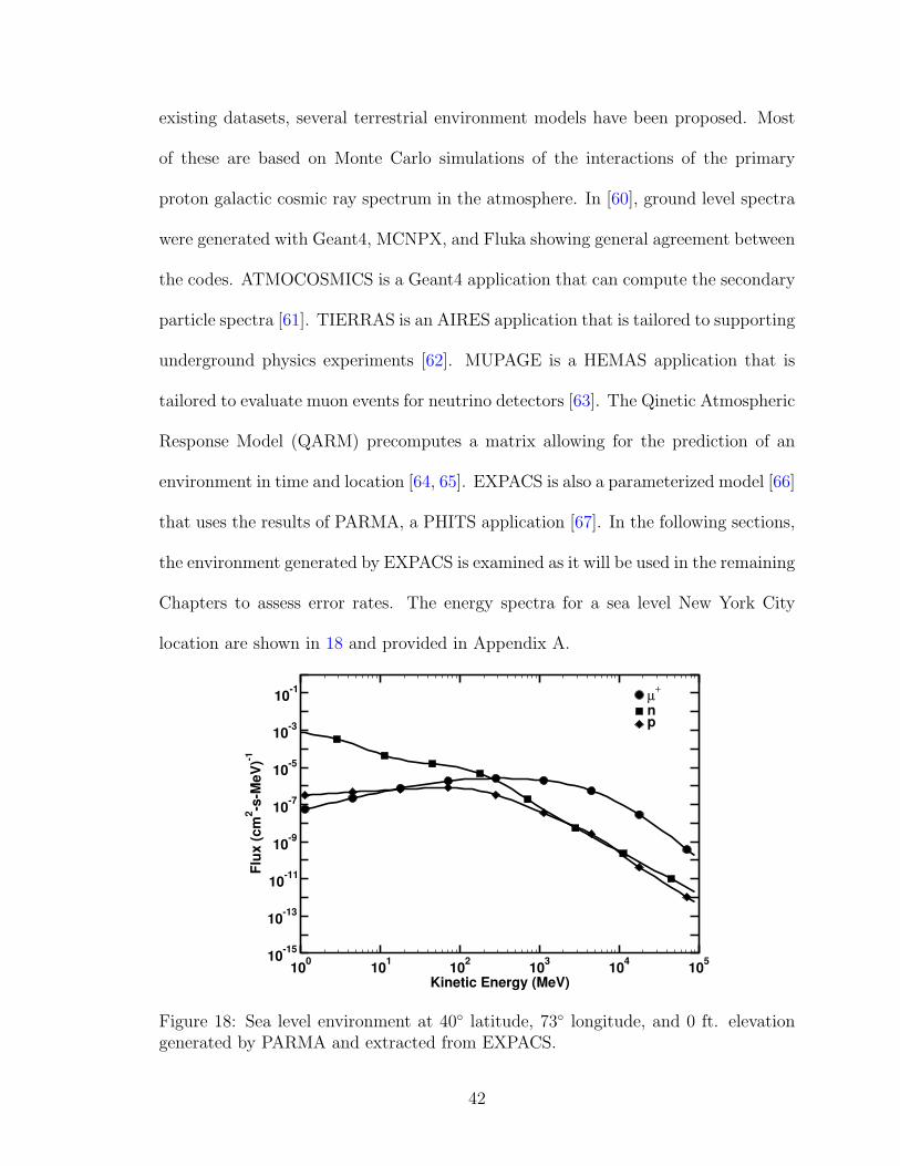
existing datasets, several terrestrial environment models have been proposed. Most
of these are based on Monte Carlo simulations of the interactions of the primary
proton galactic cosmic ray spectrum in the atmosphere. In [60], ground level spectra
were generated with Geant4, MCNPX, and Fluka showing general agreement between
the codes. ATMOCOSMICS is a Geant4 application that can compute the secondary
particle spectra [61]. TIERRAS is an AIRES application that is tailored to supporting
underground physics experiments [62]. MUPAGE is a HEMAS application that is
tailored to evaluate muon events for neutrino detectors [63]. The Qinetic Atmospheric
Response Model (QARM) precomputes a matrix allowing for the prediction of an
environment in time and location [64, 65]. EXPACS is also a parameterized model [66]
that uses the results of PARMA, a PHITS application [67]. In the following sections,
the environment generated by EXPACS is examined as it will be used in the remaining
Chapters to assess error rates. The energy spectra for a sea level New York City
location are shown in 18 and provided in Appendix A.
100
101
102
103
104
105
Kinetic Energy (MeV)
10-15
10-13
10-11
10-9
10-7
10-5
10-3
10-1
Flu
x (
cm
2-s
-MeV
)-1
µ+
np
Figure 18: Sea level environment at 40 latitude, 73 longitude, and 0 ft. elevationgenerated by PARMA and extracted from EXPACS.
42
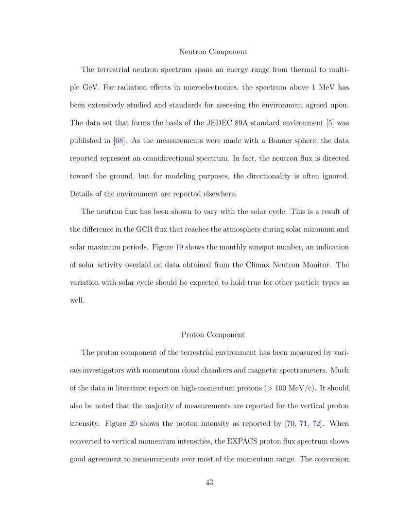
Neutron Component
The terrestrial neutron spectrum spans an energy range from thermal to multi-
ple GeV. For radiation effects in microelectronics, the spectrum above 1 MeV has
been extensively studied and standards for assessing the environment agreed upon.
The data set that forms the basis of the JEDEC 89A standard environment [5] was
published in [68]. As the measurements were made with a Bonner sphere, the data
reported represent an omnidirectional spectrum. In fact, the neutron flux is directed
toward the ground, but for modeling purposes, the directionality is often ignored.
Details of the environment are reported elsewhere.
The neutron flux has been shown to vary with the solar cycle. This is a result of
the difference in the GCR flux that reaches the atmosphere during solar minimum and
solar maximum periods. Figure 19 shows the monthly sunspot number, an indication
of solar activity overlaid on data obtained from the Climax Neutron Monitor. The
variation with solar cycle should be expected to hold true for other particle types as
well.
Proton Component
The proton component of the terrestrial environment has been measured by vari-
ous investigators with momentum cloud chambers and magnetic spectrometers. Much
of the data in literature report on high-momentum protons (> 100 MeV/c). It should
also be noted that the majority of measurements are reported for the vertical proton
intensity. Figure 20 shows the proton intensity as reported by [70, 71, 72]. When
converted to vertical momentum intensities, the EXPACS proton flux spectrum shows
good agreement to measurements over most of the momentum range. The conversion
43
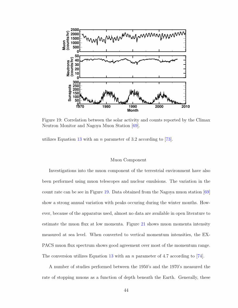
0500
1000150020002500
Muon
(counts/hr)
01020304050
Neutrons
(counts/hr)
1970 1980 1990 2000 2010Month
050
100150200250300
Sunspots
Figure 19: Correlation between the solar activity and counts reported by the ClimaxNeutron Monitor and Nagoya Muon Station [69].
utilizes Equation 13 with an n parameter of 3.2 according to [73].
Muon Component
Investigations into the muon component of the terrestrial environment have also
been performed using muon telescopes and nuclear emulsions. The variation in the
count rate can be see in Figure 19. Data obtained from the Nagoya muon station [69]
show a strong annual variation with peaks occuring during the winter months. How-
ever, because of the apparatus used, almost no data are available in open literature to
estimate the muon flux at low momenta. Figure 21 shows muon momenta intensity
measured at sea level. When converted to vertical momentum intensities, the EX-
PACS muon flux spectrum shows good agreement over most of the momentum range.
The conversion utilizes Equation 13 with an n parameter of 4.7 according to [74].
A number of studies performed between the 1950’s and the 1970’s measured the
rate of stopping muons as a function of depth beneath the Earth. Generally, these
44
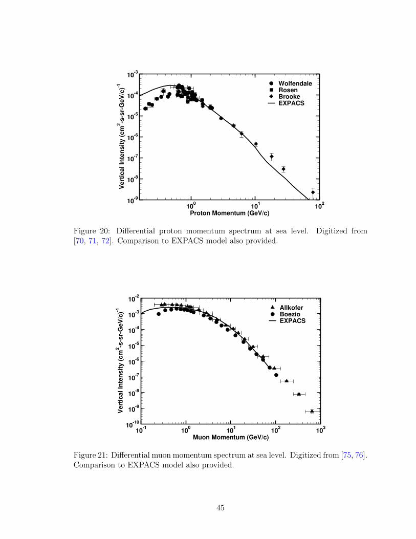
100
101
102
Proton Momentum (GeV/c)
10-9
10-8
10-7
10-6
10-5
10-4
10-3
Vert
ical In
ten
sit
y (
cm
2-s
-sr-
GeV
/c)-1 Wolfendale
RosenBrookeEXPACS
Figure 20: Differential proton momentum spectrum at sea level. Digitized from[70, 71, 72]. Comparison to EXPACS model also provided.
10-1
100
101
102
103
Muon Momentum (GeV/c)
10-10
10-9
10-8
10-7
10-6
10-5
10-4
10-3
10-2
Vert
ical In
ten
sit
y (
cm
2-s
-sr-
GeV
/c)-1 Allkofer
BoezioEXPACS
Figure 21: Differential muon momentum spectrum at sea level. Digitized from [75, 76].Comparison to EXPACS model also provided.
45

studies involved the creation and placement of a nuclear emulsion at various subter-
ranean locations. In many cases, these were Ilford G5 nuclear emulsions. After the
emulsions had been exposed for a given period of time, they were scanned for signs
of muon decays. The number of stopping muons was then used to estimate the rate
of stopping muons at the depth, in units of meters water equivalent. A compilation
of published data are presented in Figure 22.
Since no measured data on the low-energy muon energy spectra have been located
in the literature, the muon stopping data sets are an important point of validation
for any model. A comparison is drawn between the data and the energy spectra
obtained from EXPACS. Using range tables for silicon, the differential flux with
respect to energy (cm2-s-MeV)−1 is converted to a differential flux with respect to
range (cm3-s)−1. After a normalization of units, these values are overlayed on the
stopping muon data in Figure 22. The immediate agreement is fair and expected to
improve upon consideration of the axes. As the measured data represent stopping
in a nuclear emulsion with a different atomic composition and greater density, it is
expected that the silicon stopping rate should be less than that of an emulsion. In
addition, the results are reported as depth in silicon instead of water and have the
effect of stretching data towards greater depths. Under these considerations, the
model spectrum appears quite reasonable.
Conclusions
All environments present a threat to the reliable use of microelectronics due to
ionizing radiation. It is therefore important that the components of the environment
46

0 10 20 30 40 50 60 70Depth (m. w. e.)
10-7
10-6
10-5
10-4
µ S
top
pin
g R
ate
(c
m3-s
)-1
George
HallSpannagel
KanekoShortEXPACS (water)
Figure 22: The rate of stopping muons measured at various depth underground [77,78, 79, 80, 81]. Comparision to EXPACS model also provided.
are characterized. The reliability community has done this well for much of the terres-
trial and space environments providing standards for the evaluation of the effects of
altitude and latitude, as well as the natural variability. Unfortunately, the characteri-
zation has focused on the flux spectra of heavy ions and high-energy protons in space
and neutrons on Earth. The historical absence of a need for the low-energy proton and
muon environments has not motivated the characterization of these components of
operating environments. For a comprehensive approach to radiation effects, a model
of the full environment should be considered.
47
CHAPTER IV
ACCELERATED TESTING
The evaluation of a part’s radiation response is often an undertaking that requires
an accelerated test condition which can enhance the speed at which a failure mecha-
nism presents itself. Under a controlled environment, the statistics of the experiment
are greater than what can be estimated from on-orbit or in-field operation. Further,
the inability to identify a part that is not suitable for the intended radiation envi-
ronment will present extraneous costs to the mission or corporation, if not complete
failure of the system.
Accelerated testing for single event effects involves measuring an event cross-
section (i.e., the probability of event occurrence). A particle accelerator is used to
produce an enhanced flux environment. Ideally, the beam is monochromatic, pre-
senting the part with a particular species and a nearly single-valued kinetic energy,
although specialized facilities are capable of reproducing the shape of the energy
spectrum of natural environments.
In single event upset testing, the part, usually a memory, is placed in front of
the beam and irradiated while retaining data. After the irradiation, the memory is
checked for bit errors. If the device is sensitive to the incident radiation, the number of
errors observed during the test, N , will directly depend on the beam fluence, φ cm−2.
In some cases, the memory is a test array that is not production ready. The yield
of these memories may be low or unstable bits in the array may be present. Even in
the absence of radiation, after a write to the array, a read will uncover bits in error.
48

If the number of bad bits is comparable to the number of single event upsets during
a test run, they will introduce a bias into the measured cross section.
This can provide a systematic background error that must be accounted for during
the data analysis. If the number of bad bits can be measured and shown to be
independent of the time between the read and write, their effect can be removed from
the data. This implies that bad bits do not accumulate with time. Since the number
of bad bits may fluctuate as bits randomly flip, measurements will have a probabilistic
distribution. The mean value of the distribution will be referred to as µB and the
variance of the sample distribution as s2B to prevent confusion with the SEU cross
section σSEU. In this case, the variance and cross section of the number of upsets can
be calculated as:
s2SEU = |N − µB|+ s2
B (14)
σ SEU =|N − µB| ± s SEU
φ(15)
The SEU cross section is not only a result of the area presented by the target, but
also captures the probability that the particle deposits sufficient energy to evoke an
upset in the circuit. For unlikely particle interactions in the semiconductor material
to induce an upset, the SEU cross section is much smaller than the physical features
of the device. This is the case for neutron and high-energy proton-induced events.
The measured cross section is most useful as a function of the particle kinetic energy,
although for heavy ion irradiation, the particle LET is commonly used.
49
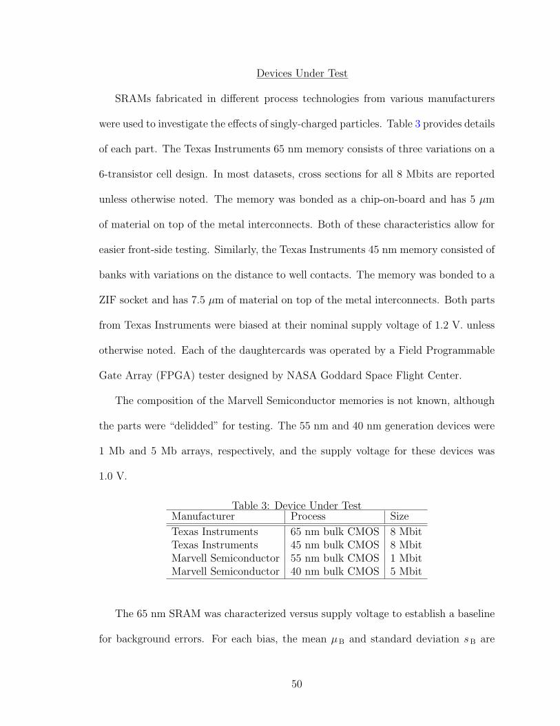
Devices Under Test
SRAMs fabricated in different process technologies from various manufacturers
were used to investigate the effects of singly-charged particles. Table 3 provides details
of each part. The Texas Instruments 65 nm memory consists of three variations on a
6-transistor cell design. In most datasets, cross sections for all 8 Mbits are reported
unless otherwise noted. The memory was bonded as a chip-on-board and has 5 µm
of material on top of the metal interconnects. Both of these characteristics allow for
easier front-side testing. Similarly, the Texas Instruments 45 nm memory consisted of
banks with variations on the distance to well contacts. The memory was bonded to a
ZIF socket and has 7.5 µm of material on top of the metal interconnects. Both parts
from Texas Instruments were biased at their nominal supply voltage of 1.2 V. unless
otherwise noted. Each of the daughtercards was operated by a Field Programmable
Gate Array (FPGA) tester designed by NASA Goddard Space Flight Center.
The composition of the Marvell Semiconductor memories is not known, although
the parts were “delidded” for testing. The 55 nm and 40 nm generation devices were
1 Mb and 5 Mb arrays, respectively, and the supply voltage for these devices was
1.0 V.
Table 3: Device Under TestManufacturer Process Size
Texas Instruments 65 nm bulk CMOS 8 MbitTexas Instruments 45 nm bulk CMOS 8 MbitMarvell Semiconductor 55 nm bulk CMOS 1 MbitMarvell Semiconductor 40 nm bulk CMOS 5 Mbit
The 65 nm SRAM was characterized versus supply voltage to establish a baseline
for background errors. For each bias, the mean µB and standard deviation sB are
50

reported in Table 4. The other SRAMs did not experience background errors when
operated at 1.0 V.
Table 4: Baseline error counts characterized versus bias for 65 nm SRAMBias (V) Runs µB sB
0.8 3 125.000 44.9520.9 10 37.100 13.6411.0 17 19.353 4.9341.1 16 8.375 2.2601.2 10 5.100 2.022
Heavy Ion Accelerated Tests
Accelerated Test Setup
Heavy ion SEU data were acquired for the Texas Instruments 65 and 45 nm
SRAMs using the facilities at the Lawrence Berkeley National Laboratories (LBNL)
and Texas A&M University (TAMU). Both facilities use a cyclotron to accelerate
ions to the device under test. The LBNL cyclotron offers a cocktail of ions up to 30
MeV/nucleon, although experimental beams up to 32 MeV/nucleon are available and
were used for this experiment. The TAMU cyclotron offers ions up to 40 MeV/nucleon
which allows testing with ions with lower LET.
The choices of ion species and energy for the 65 and 45 nm memories are listed
in Tables 5 and 6, respectively. The 45 nm memory was not available for the test
opportunity at TAMU so we do not have data at LET < 1 MeV-cm2/mg. In many
test campaigns, these data are not collected because of limited resources for testing
at high-energy facilities. The data collected on the 45 nm memory is as complete as
is often acquired. For arguments presented later, the low-LET cross sections have
51
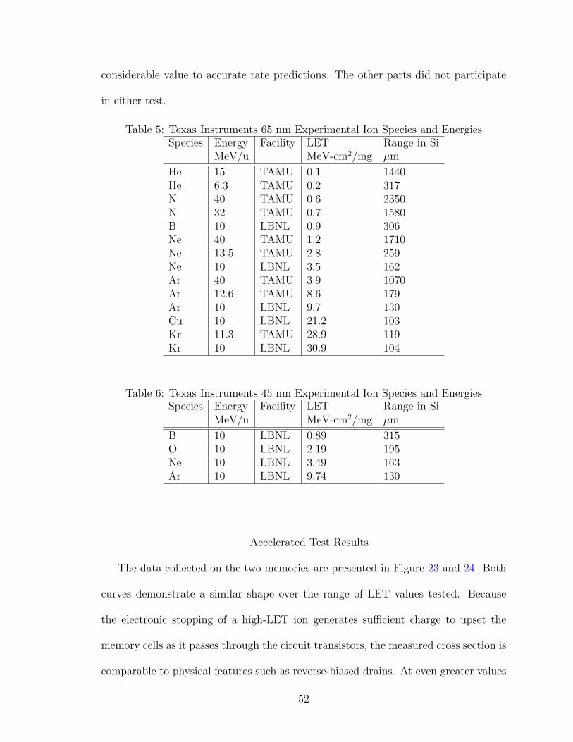
considerable value to accurate rate predictions. The other parts did not participate
in either test.
Table 5: Texas Instruments 65 nm Experimental Ion Species and EnergiesSpecies Energy Facility LET Range in Si
MeV/u MeV-cm2/mg µm
He 15 TAMU 0.1 1440He 6.3 TAMU 0.2 317N 40 TAMU 0.6 2350N 32 TAMU 0.7 1580B 10 LBNL 0.9 306Ne 40 TAMU 1.2 1710Ne 13.5 TAMU 2.8 259Ne 10 LBNL 3.5 162Ar 40 TAMU 3.9 1070Ar 12.6 TAMU 8.6 179Ar 10 LBNL 9.7 130Cu 10 LBNL 21.2 103Kr 11.3 TAMU 28.9 119Kr 10 LBNL 30.9 104
Table 6: Texas Instruments 45 nm Experimental Ion Species and EnergiesSpecies Energy Facility LET Range in Si
MeV/u MeV-cm2/mg µm
B 10 LBNL 0.89 315O 10 LBNL 2.19 195Ne 10 LBNL 3.49 163Ar 10 LBNL 9.74 130
Accelerated Test Results
The data collected on the two memories are presented in Figure 23 and 24. Both
curves demonstrate a similar shape over the range of LET values tested. Because
the electronic stopping of a high-LET ion generates sufficient charge to upset the
memory cells as it passes through the circuit transistors, the measured cross section is
comparable to physical features such as reverse-biased drains. At even greater values
52
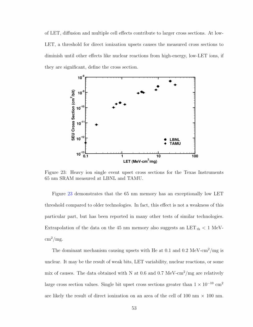
of LET, diffusion and multiple cell effects contribute to larger cross sections. At low-
LET, a threshold for direct ionization upsets causes the measured cross sections to
diminish until other effects like nuclear reactions from high-energy, low-LET ions, if
they are significant, define the cross section.
0.1 1 10 100
LET (MeV-cm2/mg)
10-13
10-12
10-11
10-10
10-9
10-8
SE
U C
ross S
ecti
on
(cm
2/b
it)
LBNLTAMU
Figure 23: Heavy ion single event upset cross sections for the Texas Instruments65 nm SRAM measured at LBNL and TAMU.
Figure 23 demonstrates that the 65 nm memory has an exceptionally low LET
threshold compared to older technologies. In fact, this effect is not a weakness of this
particular part, but has been reported in many other tests of similar technologies.
Extrapolation of the data on the 45 nm memory also suggests an LET th < 1 MeV-
cm2/mg.
The dominant mechanism causing upsets with He at 0.1 and 0.2 MeV-cm2/mg is
unclear. It may be the result of weak bits, LET variability, nuclear reactions, or some
mix of causes. The data obtained with N at 0.6 and 0.7 MeV-cm2/mg are relatively
large cross section values. Single bit upset cross sections greater than 1× 10⁻¹⁰ cm2
are likely the result of direct ionization on an area of the cell of 100 nm × 100 nm.
53
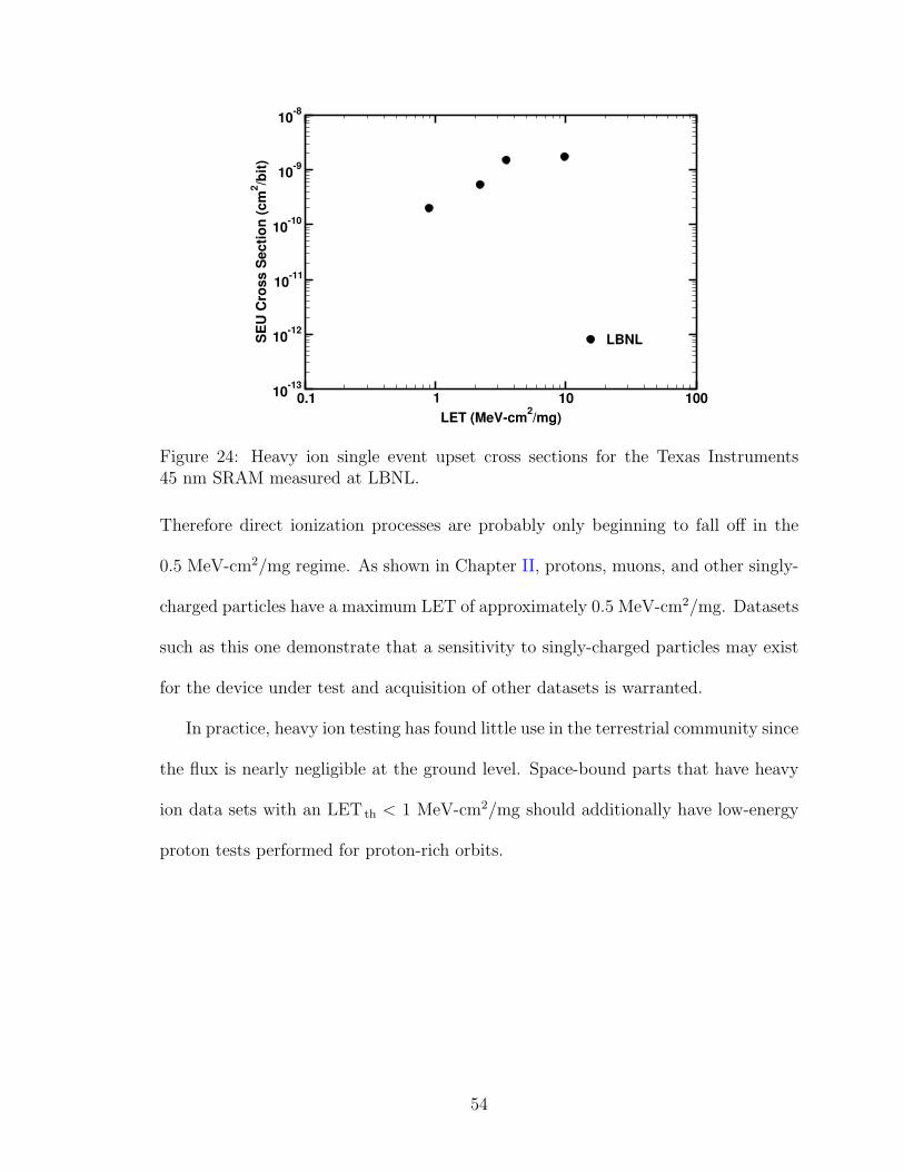
0.1 1 10 100
LET (MeV-cm2/mg)
10-13
10-12
10-11
10-10
10-9
10-8
SE
U C
ross S
ecti
on
(cm
2/b
it)
LBNL
Figure 24: Heavy ion single event upset cross sections for the Texas Instruments45 nm SRAM measured at LBNL.
Therefore direct ionization processes are probably only beginning to fall off in the
0.5 MeV-cm2/mg regime. As shown in Chapter II, protons, muons, and other singly-
charged particles have a maximum LET of approximately 0.5 MeV-cm2/mg. Datasets
such as this one demonstrate that a sensitivity to singly-charged particles may exist
for the device under test and acquisition of other datasets is warranted.
In practice, heavy ion testing has found little use in the terrestrial community since
the flux is nearly negligible at the ground level. Space-bound parts that have heavy
ion data sets with an LET th < 1 MeV-cm2/mg should additionally have low-energy
proton tests performed for proton-rich orbits.
54
Proton Accelerated Testing
Accelerated Test Setup
Proton single event upset data were collected for the Texas Instruments 65 and
45 nm memories over a wide energy range at four facilities. The cyclotron at Indiana
University [82] was used to obtain cross sections at 198 and 98 MeV. A 63.3 MeV
proton beam at UC Davis [83] was used (with degraders) to obtain data as low as 19.8
MeV and a 14.6 MeV primary beam was degraded to obtain data down to 2.6 MeV.
The low-energy (< 2 MeV) data were acquired at NASA GSFC’s Van de Graaff
facility. The LBNL cyclotron was used to confirm the measured proton cross section
at 32.5 MeV. Additionally a 6 MeV H2+ beam was broken up and degraded through
air to obtain a proton spectrum with a peak as low as 1.2 MeV.
Figure 25 shows the proton energy spectrum at LBNL measured with a surface
barrier detector. The 1.2 MeV beam was used in the test on the 65 nm SRAM. The
1.7 and 1.4 MeV beams were measured with a different calorimetry setup at a later
date and therefore appear less well-defined. These beams were used to test the 45 nm
SRAM. The spectrum demonstrates that the dosimetry is one difficultly associated
with low-energy proton testing. In order to measure the flux during a test, the counts
on the SBD were used to calibrate the counts observed on the photo multiplier tubes
upstream.
Similar difficulties arose with the tests performed at UC Davis. The primary
beams used were 63.3 MeV and 14.6 MeV. Other energies were obtained through the
use of degraders. The composition and thickness of the degraders were modeled and
simulated in MRED to obtain the energy spectrum observed by the part. Figure 26
55

shows the result of the simulations.
A similar analysis was performed for the TRIUMF 65 MeV proton beam, although
no test data were obtained with this beam line. The beam line at TRIUMF is another
possible choice for moderate proton energies therefore an analysis has been included
at the end of the chapter. Low energy tests could be developed to use this beam line.
Whether the tests were performed with the cyclotron at UC Davis or TRIUMF, a
degraded beam has some undesirable characteristics. In the simulations of a 60+ MeV
beam degraded to less than 20 MeV, the distribution of incident energies is very broad.
Although no beam is truly monochromatic, the range of energies produced by this
setup may cover a region of the device response that is rapidly changing with energy.
The setup for low-energy proton tests at LBNL required that the test be performed
in air rather than in the vacuum chamber. Since protons at these energies have very
limited range, the device was placed as close to the beam window as possible as shown
in Figure 27. The effect of the air introduces straggling and systematic error in the
cross section measurement.
Accelerated Test Results
The experimental proton-induced SEU cross section curves for the 65 and 45 nm
memories are shown in Figures 28 and 29, respectively. The cross section measure-
ments at proton energies above 10 MeV look similar to almost any other part. The
value is nearly constant up to the highest energies tested. This portion of the curve is
dominated by particle-reaction-induced events since at these energies protons are well
above the Coulomb barrier. A proton that strikes a nucleus near the active region of
an SRAM cell causes secondary charged particles to ionize the material and generate
56
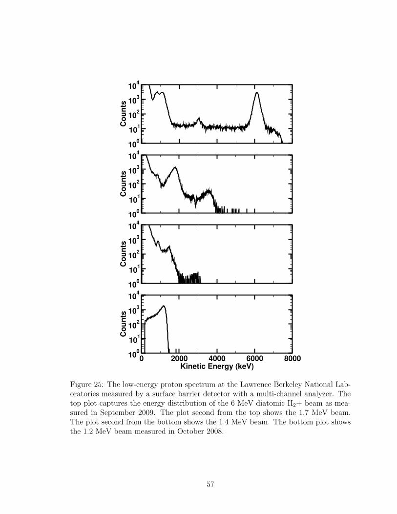
100
101
102
103
104
Co
un
ts
100
101
102
103
104
Co
un
ts
100
101
102
103
104
Co
un
ts
0 2000 4000 6000 8000Kinetic Energy (keV)
100
101
102
103
104
Co
un
ts
Figure 25: The low-energy proton spectrum at the Lawrence Berkeley National Lab-oratories measured by a surface barrier detector with a multi-channel analyzer. Thetop plot captures the energy distribution of the 6 MeV diatomic H2+ beam as mea-sured in September 2009. The plot second from the top shows the 1.7 MeV beam.The plot second from the bottom shows the 1.4 MeV beam. The bottom plot showsthe 1.2 MeV beam measured in October 2008.
57
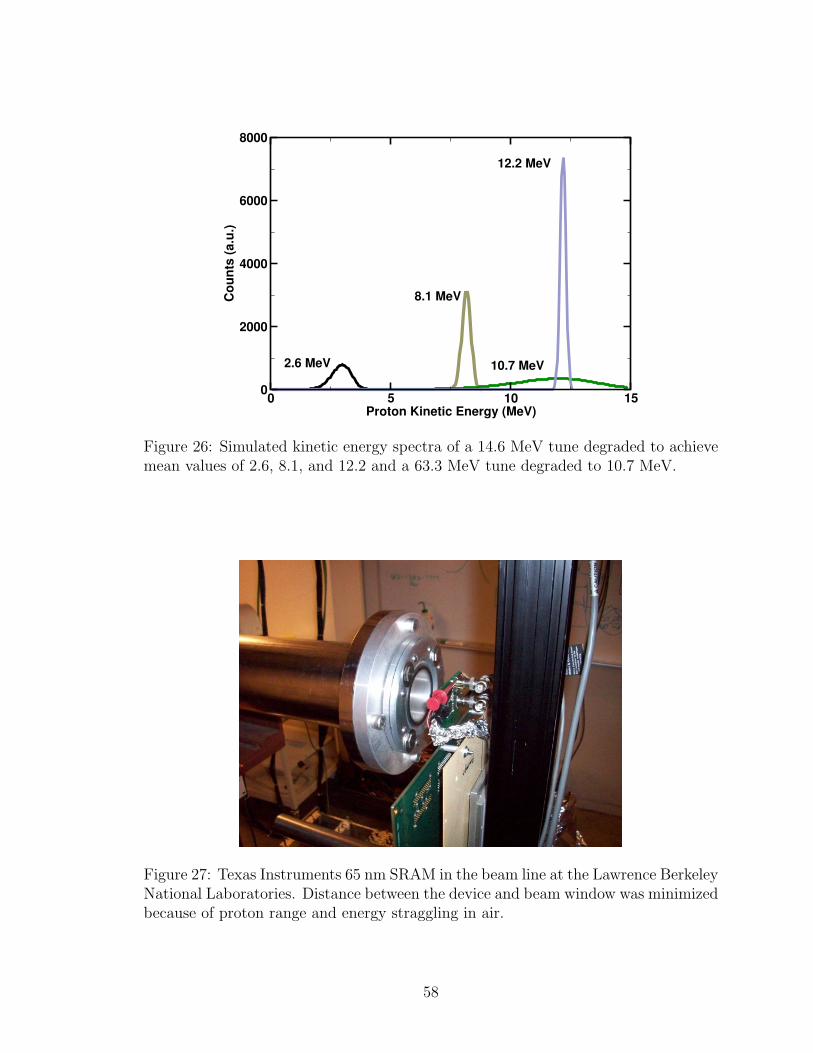
0 5 10 15Proton Kinetic Energy (MeV)
0
2000
4000
6000
8000
Co
un
ts (
a.u
.)
2.6 MeV
8.1 MeV
10.7 MeV
12.2 MeV
Figure 26: Simulated kinetic energy spectra of a 14.6 MeV tune degraded to achievemean values of 2.6, 8.1, and 12.2 and a 63.3 MeV tune degraded to 10.7 MeV.
Figure 27: Texas Instruments 65 nm SRAM in the beam line at the Lawrence BerkeleyNational Laboratories. Distance between the device and beam window was minimizedbecause of proton range and energy straggling in air.
58

enough charge to upset the circuit. The cross section is consistent with what one
would expect from nuclear reaction events. Assuming a one micrometer collection
depth, and a 0.5× 10⁻⁸ cm2 cell area, applying Equation 3 yields 5× 10⁻¹⁴ cm2.
Classical proton and neutron cross sections roll off at energies of 10 MeV or higher.
Neither of these datasets does. Between 2 and 10 MeV the cross sections appear
slightly elevated from the values at higher energies. As discussed in Chapter II,
protons at this energy are nearing the Coulomb barrier which prevents the particle
from initiating a particle reaction. Instead the proton is likely displacing a silicon or
oxygen nucleus from the crystal lattice through an elastic scattering event. It is also
possible that some enhancement in the cross section was caused by the degrading of
the beam.
At energies below 2 MeV the proton cross-section curves demonstrate the charac-
teristics expected when direct ionization dominates the other upset mechanisms. The
beam energy is below the Coulomb barrier for the common materials and the range
of the recoil is increasingly limited. The three orders of magnitude increase in cross
section going from high energy (> 10 MeV) to low energy (< 2 MeV) indicates a clear
transition from upsets due to nuclear elastic and inelastic events to direct ionization.
At these low energies, the proton cross section is on the order of the dimensions of
the physical features of the cell, consistent with direct ionization.
59
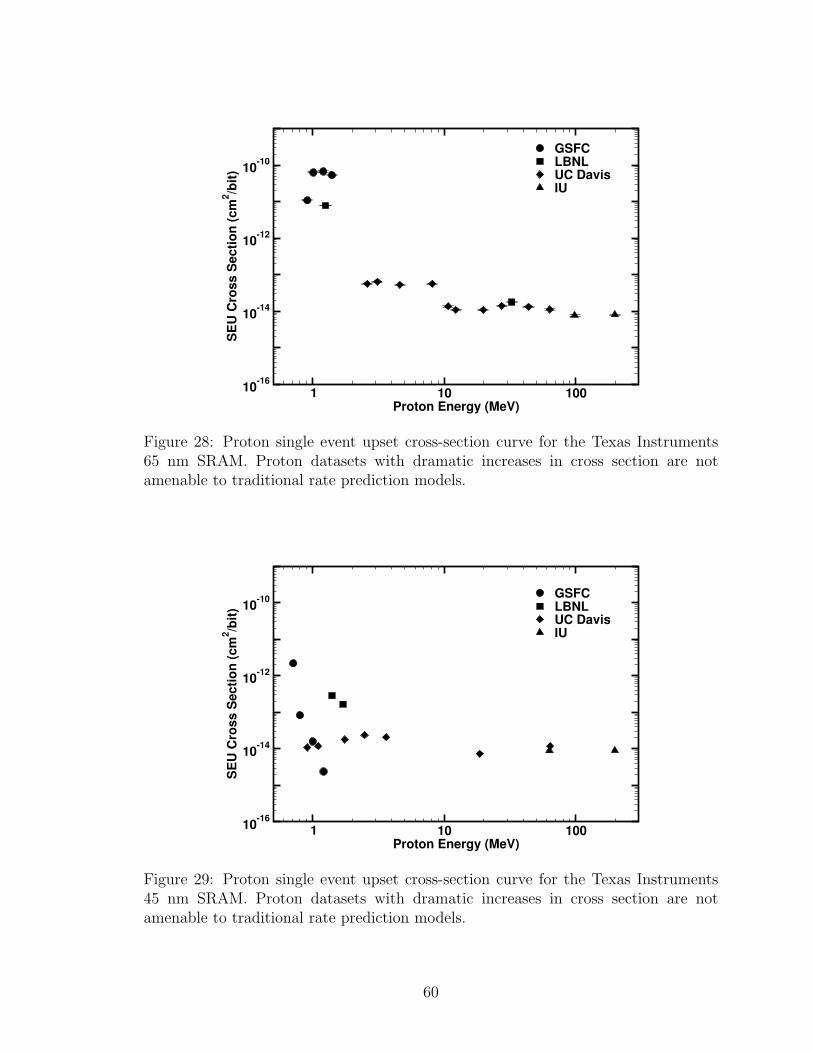
1 10 100Proton Energy (MeV)
10-16
10-14
10-12
10-10
SE
U C
ros
s S
ec
tio
n (
cm
2/b
it)
GSFCLBNLUC DavisIU
Figure 28: Proton single event upset cross-section curve for the Texas Instruments65 nm SRAM. Proton datasets with dramatic increases in cross section are notamenable to traditional rate prediction models.
1 10 100Proton Energy (MeV)
10-16
10-14
10-12
10-10
SE
U C
ros
s S
ec
tio
n (
cm
2/b
it)
GSFCLBNLUC DavisIU
Figure 29: Proton single event upset cross-section curve for the Texas Instruments45 nm SRAM. Proton datasets with dramatic increases in cross section are notamenable to traditional rate prediction models.
60
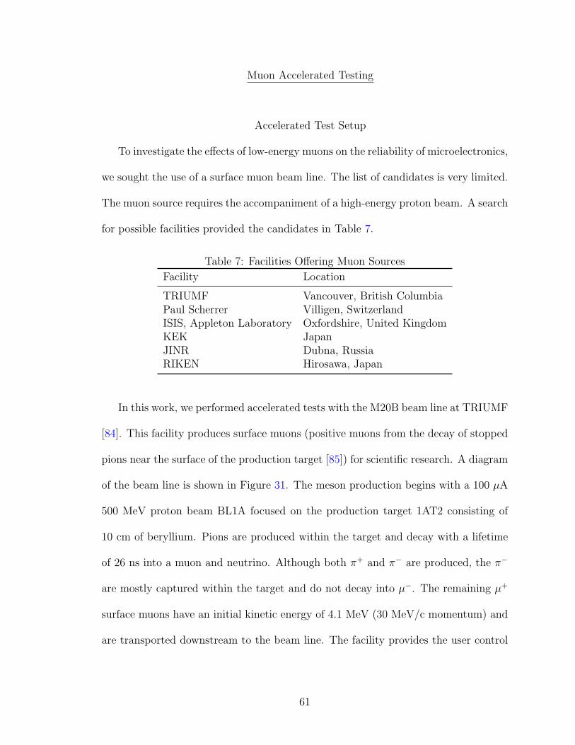
Muon Accelerated Testing
Accelerated Test Setup
To investigate the effects of low-energy muons on the reliability of microelectronics,
we sought the use of a surface muon beam line. The list of candidates is very limited.
The muon source requires the accompaniment of a high-energy proton beam. A search
for possible facilities provided the candidates in Table 7.
Table 7: Facilities Offering Muon Sources
Facility Location
TRIUMF Vancouver, British ColumbiaPaul Scherrer Villigen, SwitzerlandISIS, Appleton Laboratory Oxfordshire, United KingdomKEK JapanJINR Dubna, RussiaRIKEN Hirosawa, Japan
In this work, we performed accelerated tests with the M20B beam line at TRIUMF
[84]. This facility produces surface muons (positive muons from the decay of stopped
pions near the surface of the production target [85]) for scientific research. A diagram
of the beam line is shown in Figure 31. The meson production begins with a 100 µA
500 MeV proton beam BL1A focused on the production target 1AT2 consisting of
10 cm of beryllium. Pions are produced within the target and decay with a lifetime
of 26 ns into a muon and neutrino. Although both π+ and π− are produced, the π−
are mostly captured within the target and do not decay into µ−. The remaining µ+
surface muons have an initial kinetic energy of 4.1 MeV (30 MeV/c momentum) and
are transported downstream to the beam line. The facility provides the user control
61

over a dipole magnet (M20B1) to select particle momentum, followed by variable-
width slits (M20SL1) for refinement. Following a second bending magnet (M20B2),
an electrostatic separator (M20BSEP) provides velocity selection. Finally, a second
set of slits (M20BSL2) is used for collimation and the beam is brought to the final
focus.
26.5 27 27.5 28 28.5 29 29.5 30 30.5 31 31.5Muon Momentum (MeV/c)
0
0.4
0.8
1.2
1.6
2
2.4
2.8
3.2
3.6
Mu
on
Ra
te (
arb
itra
ry u
nit
s)
Slit = 40 mmSlit = 100 mm
Figure 30: The surface muon momentum produced by the M20B beamline at TRI-UMF [86].
Given the momentum and velocity selections in the beam line and the energy
deposition in a surface barrier detector (discussed in the following subsection) the
mass of the accelerated particles is known to be 106 MeV/c2. Positively-charged
particles of different mass such as pions (140 MeV/c2) and protons (938 MeV/c2)
are clearly eliminated. For instance, 420 keV protons match the 28 MeV/c channel
momentum but are deflected away in the electrostatic separator. Similarly, pions are
removed by the separator and further decay with a mean decay length of about 2 m.
After traversing the 20 m channel length all pions are eliminated.
Positrons, while deflected by the magnets and separators upstream, are present
62
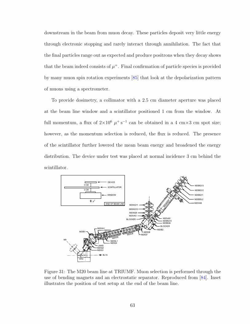
downstream in the beam from muon decay. These particles deposit very little energy
through electronic stopping and rarely interact through annihilation. The fact that
the final particles range out as expected and produce positrons when they decay shows
that the beam indeed consists of µ+. Final confirmation of particle species is provided
by many muon spin rotation experiments [85] that look at the depolarization pattern
of muons using a spectrometer.
To provide dosimetry, a collimator with a 2.5 cm diameter aperture was placed
at the beam line window and a scintillator positioned 1 cm from the window. At
full momentum, a flux of 2×10⁶ µ+ s−1 can be obtained in a 4 cm×3 cm spot size;
however, as the momentum selection is reduced, the flux is reduced. The presence
of the scintillator further lowered the mean beam energy and broadened the energy
distribution. The device under test was placed at normal incidence 3 cm behind the
scintillator.
Figure 31: The M20 beam line at TRIUMF. Muon selection is performed through theuse of bending magnets and an electrostatic separator. Reproduced from [84]. Insetillustrates the position of test setup at the end of the beam line.
63
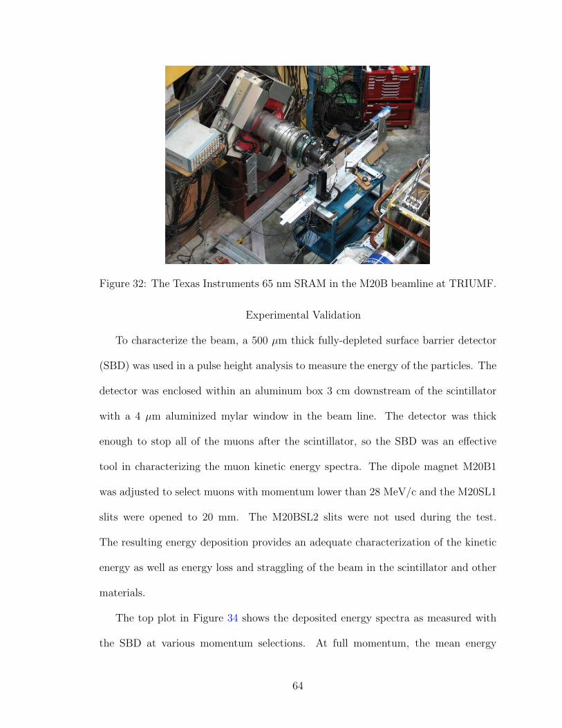
Figure 32: The Texas Instruments 65 nm SRAM in the M20B beamline at TRIUMF.
Experimental Validation
To characterize the beam, a 500 µm thick fully-depleted surface barrier detector
(SBD) was used in a pulse height analysis to measure the energy of the particles. The
detector was enclosed within an aluminum box 3 cm downstream of the scintillator
with a 4 µm aluminized mylar window in the beam line. The detector was thick
enough to stop all of the muons after the scintillator, so the SBD was an effective
tool in characterizing the muon kinetic energy spectra. The dipole magnet M20B1
was adjusted to select muons with momentum lower than 28 MeV/c and the M20SL1
slits were opened to 20 mm. The M20BSL2 slits were not used during the test.
The resulting energy deposition provides an adequate characterization of the kinetic
energy as well as energy loss and straggling of the beam in the scintillator and other
materials.
The top plot in Figure 34 shows the deposited energy spectra as measured with
the SBD at various momentum selections. At full momentum, the mean energy
64
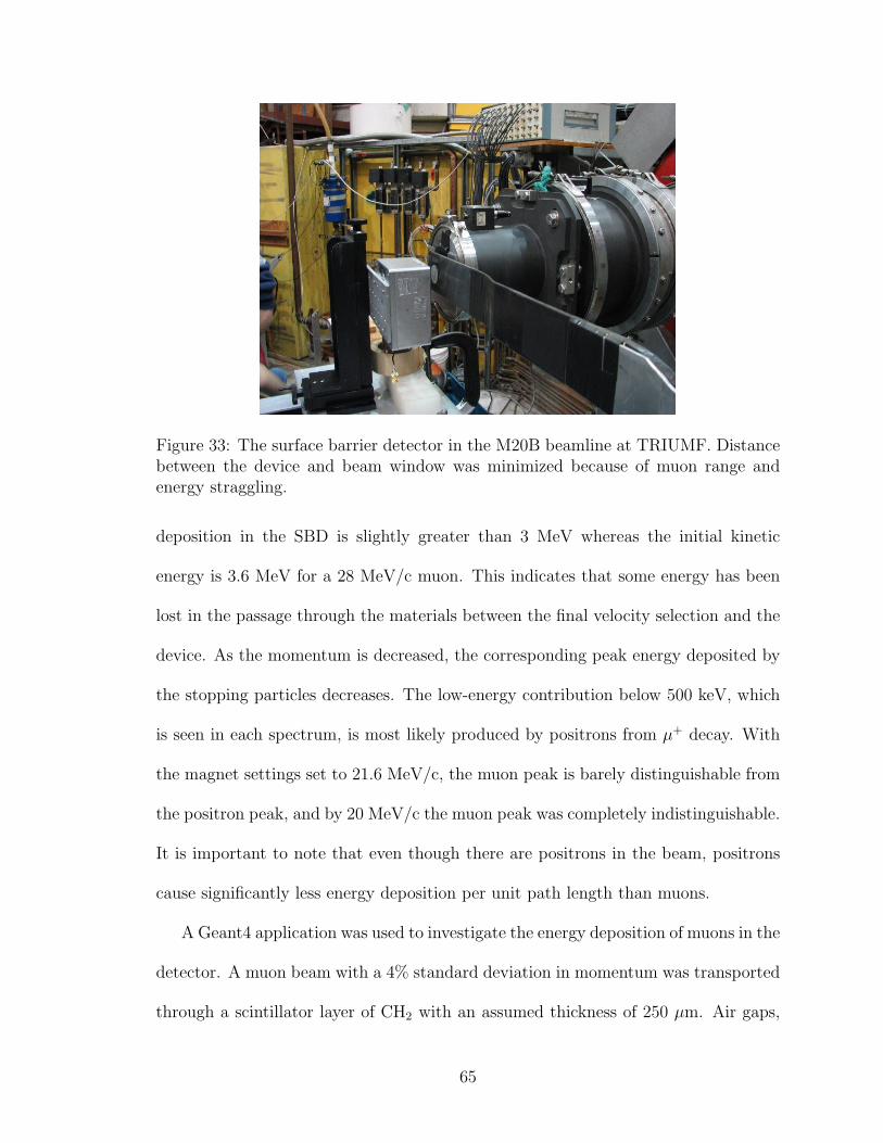
Figure 33: The surface barrier detector in the M20B beamline at TRIUMF. Distancebetween the device and beam window was minimized because of muon range andenergy straggling.
deposition in the SBD is slightly greater than 3 MeV whereas the initial kinetic
energy is 3.6 MeV for a 28 MeV/c muon. This indicates that some energy has been
lost in the passage through the materials between the final velocity selection and the
device. As the momentum is decreased, the corresponding peak energy deposited by
the stopping particles decreases. The low-energy contribution below 500 keV, which
is seen in each spectrum, is most likely produced by positrons from µ+ decay. With
the magnet settings set to 21.6 MeV/c, the muon peak is barely distinguishable from
the positron peak, and by 20 MeV/c the muon peak was completely indistinguishable.
It is important to note that even though there are positrons in the beam, positrons
cause significantly less energy deposition per unit path length than muons.
A Geant4 application was used to investigate the energy deposition of muons in the
detector. A muon beam with a 4% standard deviation in momentum was transported
through a scintillator layer of CH2 with an assumed thickness of 250 µm. Air gaps,
65
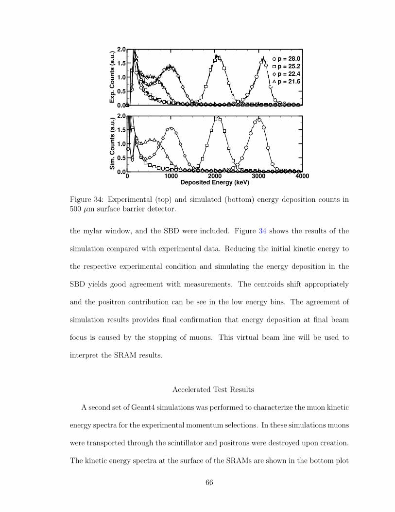
0.0
0.5
1.0
1.5
2.0
Ex
p.
Co
un
ts (
a.u
.)
p = 28.0
p = 25.2
p = 22.4
p = 21.6
0 1000 2000 3000 4000Deposited Energy (keV)
0.0
0.5
1.0
1.5
2.0S
im.
Co
un
ts (
a.u
.)
Figure 34: Experimental (top) and simulated (bottom) energy deposition counts in500 µm surface barrier detector.
the mylar window, and the SBD were included. Figure 34 shows the results of the
simulation compared with experimental data. Reducing the initial kinetic energy to
the respective experimental condition and simulating the energy deposition in the
SBD yields good agreement with measurements. The centroids shift appropriately
and the positron contribution can be see in the low energy bins. The agreement of
simulation results provides final confirmation that energy deposition at final beam
focus is caused by the stopping of muons. This virtual beam line will be used to
interpret the SRAM results.
Accelerated Test Results
A second set of Geant4 simulations was performed to characterize the muon kinetic
energy spectra for the experimental momentum selections. In these simulations muons
were transported through the scintillator and positrons were destroyed upon creation.
The kinetic energy spectra at the surface of the SRAMs are shown in the bottom plot
66
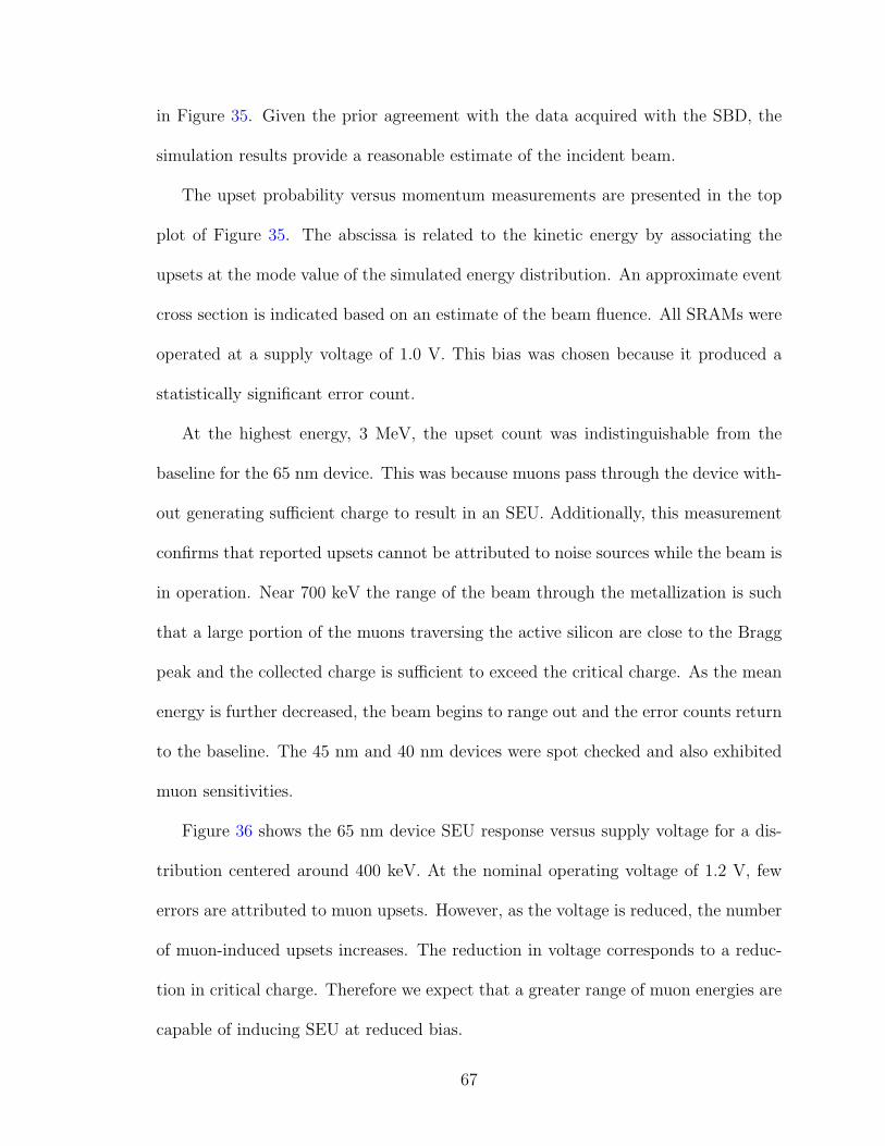
in Figure 35. Given the prior agreement with the data acquired with the SBD, the
simulation results provide a reasonable estimate of the incident beam.
The upset probability versus momentum measurements are presented in the top
plot of Figure 35. The abscissa is related to the kinetic energy by associating the
upsets at the mode value of the simulated energy distribution. An approximate event
cross section is indicated based on an estimate of the beam fluence. All SRAMs were
operated at a supply voltage of 1.0 V. This bias was chosen because it produced a
statistically significant error count.
At the highest energy, 3 MeV, the upset count was indistinguishable from the
baseline for the 65 nm device. This was because muons pass through the device with-
out generating sufficient charge to result in an SEU. Additionally, this measurement
confirms that reported upsets cannot be attributed to noise sources while the beam is
in operation. Near 700 keV the range of the beam through the metallization is such
that a large portion of the muons traversing the active silicon are close to the Bragg
peak and the collected charge is sufficient to exceed the critical charge. As the mean
energy is further decreased, the beam begins to range out and the error counts return
to the baseline. The 45 nm and 40 nm devices were spot checked and also exhibited
muon sensitivities.
Figure 36 shows the 65 nm device SEU response versus supply voltage for a dis-
tribution centered around 400 keV. At the nominal operating voltage of 1.2 V, few
errors are attributed to muon upsets. However, as the voltage is reduced, the number
of muon-induced upsets increases. The reduction in voltage corresponds to a reduc-
tion in critical charge. Therefore we expect that a greater range of muon energies are
capable of inducing SEU at reduced bias.
67
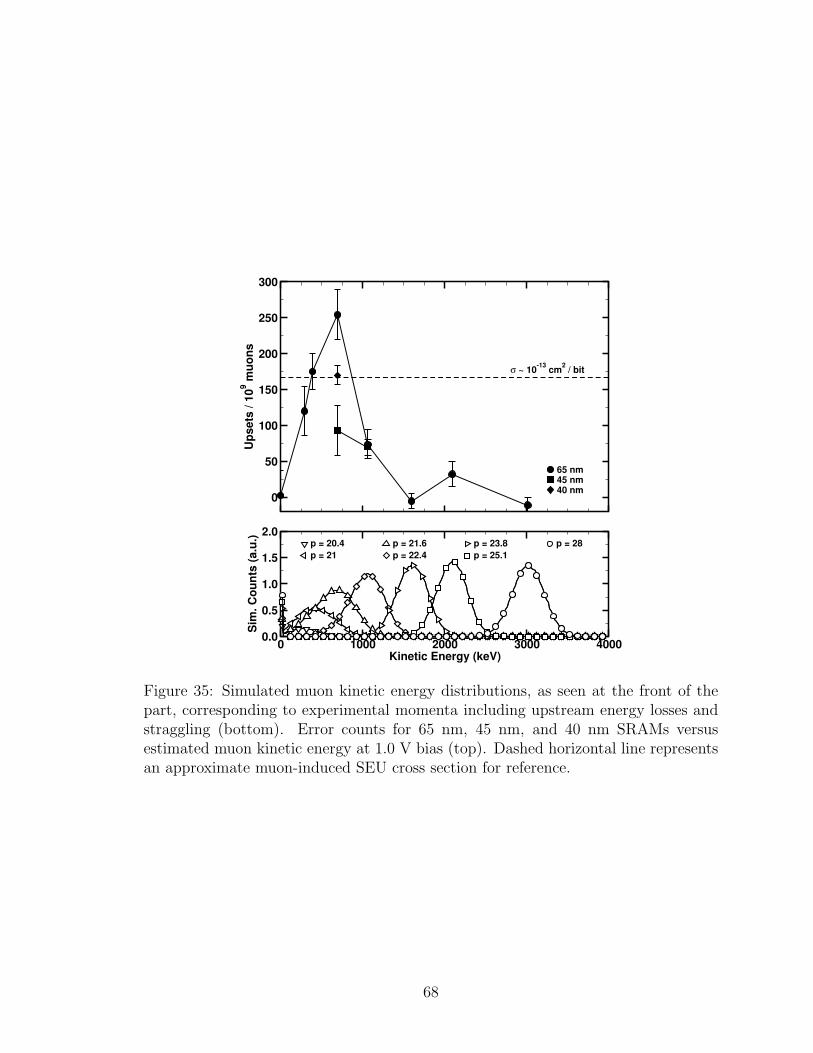
0 1000 2000 3000 4000Kinetic Energy (keV)
0.0
0.5
1.0
1.5
2.0
Sim
. C
ou
nts
(a.u
.)
0
50
100
150
200
250
300
Up
sets
/ 1
09 m
uo
ns
65 nm45 nm40 nm
p = 20.4
p = 21
p = 21.6
p = 22.4
p = 23.8
p = 25.1
p = 28
σ ~ 10-13
cm2 / bit
Figure 35: Simulated muon kinetic energy distributions, as seen at the front of thepart, corresponding to experimental momenta including upstream energy losses andstraggling (bottom). Error counts for 65 nm, 45 nm, and 40 nm SRAMs versusestimated muon kinetic energy at 1.0 V bias (top). Dashed horizontal line representsan approximate muon-induced SEU cross section for reference.
68
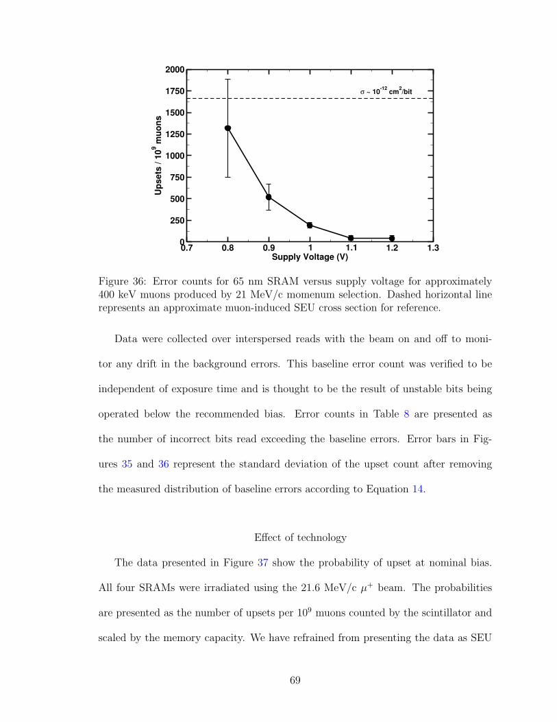
0.7 0.8 0.9 1 1.1 1.2 1.3Supply Voltage (V)
0
250
500
750
1000
1250
1500
1750
2000
Up
sets
/ 1
09 m
uo
ns
σ ~ 10-12
cm2/bit
Figure 36: Error counts for 65 nm SRAM versus supply voltage for approximately400 keV muons produced by 21 MeV/c momenum selection. Dashed horizontal linerepresents an approximate muon-induced SEU cross section for reference.
Data were collected over interspersed reads with the beam on and off to moni-
tor any drift in the background errors. This baseline error count was verified to be
independent of exposure time and is thought to be the result of unstable bits being
operated below the recommended bias. Error counts in Table 8 are presented as
the number of incorrect bits read exceeding the baseline errors. Error bars in Fig-
ures 35 and 36 represent the standard deviation of the upset count after removing
the measured distribution of baseline errors according to Equation 14.
Effect of technology
The data presented in Figure 37 show the probability of upset at nominal bias.
All four SRAMs were irradiated using the 21.6 MeV/c µ+ beam. The probabilities
are presented as the number of upsets per 109 muons counted by the scintillator and
scaled by the memory capacity. We have refrained from presenting the data as SEU
69
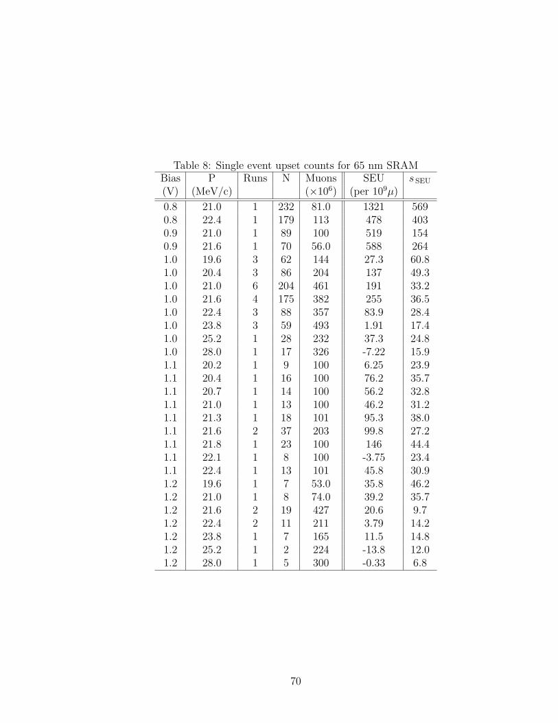
Table 8: Single event upset counts for 65 nm SRAMBias P Runs N Muons SEU s SEU
(V) (MeV/c) (×106) (per 109µ)
0.8 21.0 1 232 81.0 1321 5690.8 22.4 1 179 113 478 4030.9 21.0 1 89 100 519 1540.9 21.6 1 70 56.0 588 2641.0 19.6 3 62 144 27.3 60.81.0 20.4 3 86 204 137 49.31.0 21.0 6 204 461 191 33.21.0 21.6 4 175 382 255 36.51.0 22.4 3 88 357 83.9 28.41.0 23.8 3 59 493 1.91 17.41.0 25.2 1 28 232 37.3 24.81.0 28.0 1 17 326 -7.22 15.91.1 20.2 1 9 100 6.25 23.91.1 20.4 1 16 100 76.2 35.71.1 20.7 1 14 100 56.2 32.81.1 21.0 1 13 100 46.2 31.21.1 21.3 1 18 101 95.3 38.01.1 21.6 2 37 203 99.8 27.21.1 21.8 1 23 100 146 44.41.1 22.1 1 8 100 -3.75 23.41.1 22.4 1 13 101 45.8 30.91.2 19.6 1 7 53.0 35.8 46.21.2 21.0 1 8 74.0 39.2 35.71.2 21.6 2 19 427 20.6 9.71.2 22.4 2 11 211 3.79 14.21.2 23.8 1 7 165 11.5 14.81.2 25.2 1 2 224 -13.8 12.01.2 28.0 1 5 300 -0.33 6.8
70

cross sections to emphasize that the beam was not monoenergetic.
40 45 55 65Technology Node (nm)
0
5
10
15
20
25
Up
se
ts /
10
9 m
uo
ns
/ M
b
Figure 37: Experimental muon-induced single event upset probability for each deviceunder test operated at nominal supply voltage. Momentum selection was 21.6 MeV/c.
These data show a clear increase in the SEU susceptibility and significance of
energy deposition by muons for scaled technologies. To first order, the reduction of
the device area results in a decrease in the number of particles passing through the
cell and capable of producing an upset. This scaling would reduce the probability of
a bit being in error in the beam. The increase in upset probability is therefore due
to differences in the geometry of the charge collection, an increase in the fluence of
energy deposition events exceeding the critical charge, or both.
Further, in these experiments, the incident muons have a distribution of kinetic
energies and therefore a distribution of stopping powers. As the technology node
decreases, the charge required to upset a single memory cell decreases. The effect of
this trend is an increase in the fraction of the distribution that is able to induce an
upset. For the 40 nm SRAM, a larger portion of the 21.6 MeV/c beam exceeds the
stopping power threshold as compared with the 65 nm SRAM. While the probability
71
of upset is increasing for future devices, it cannot be ascertained from these data
whether the trend is linearly or super-linearly increasing.
Hardness Assurance Methods
Recommendations
Our results show, for some environments, that direct ionization from low-energy
protons will be a significant factor affecting the overall error rate. If it is believed
that a component is susceptible to upset from the direct ionization of a proton,
characterizing the low-energy proton SEU cross section will be imperative. Therefore
the implications for hardness assurance are considered and the following sequence of
steps to qualify the component for space applications have been developed with the
advisement of investigators at NASA Goddard.
Step 1: Measure the upset cross section with long range, low-LET
light ions. In general, soft error rate prediction techniques derived from accelerated
testing require that the stopping power of the incident particle is known as it traverses
through the device. Low-energy proton testing is conducted using proton beams with
energies at or below 2 MeV, such that the particles are at or near end-of-range. This
is done to achieve mass stopping powers – LETs – large enough to cause single-event
upset through direct ionization from the primary beam.
The SRIM-calculated mass stopping power of protons incident on silicon is com-
pared to data from Helmut Paul’s database [87] in Figure 38. It agrees well with the
majority of data presented, though the large spread in experimental mass stopping
powers below 1 MeV is apparent. It is generally true that experimental errors in
72

102
103
104
105
106
107
108
Proton Kinetic Energy (eV)
0
0.1
0.2
0.3
0.4
0.5
0.6
0.7
Ele
ctr
on
ic S
top
pin
g P
ow
er
((M
eV
⋅c
m2)/
mg
)
Experimental Data
SRIM 2008
Figure 38: A comparison of experimental and calculated mass stopping power forhydrogen on silicon. The experimental data are taken from H. Paul’s database [87]and the calculated values are from SRIM-2008.04 [89]. Note that as proton energydecreases, the uncertainty in the experimental mass stopping power increases.
measuring stopping powers increases with decreasing energy [88]. For transmission
measurements at low energy, thin foils are needed. This makes the presence of pin
holes, surface impurities, and thickness variations detrimental to the measurement.
Furthermore, the critical angle for channeling increases at low energy along with the
importance of multiple scattering. These facts translate to uncertainty in stopping
power formulations that rely on these data, which includes SRIM and codes based on
ICRU Report 49 [36], such as Geant4.
Alternatively, ions having greater mass, must be accelerated to higher energy to
achieve a similar stopping power. Thus they have increased range and reduced strag-
gling, both issues that plague low-energy proton testing. The energy loss of higher-
energy ions will be less sensitive to variations in materials as they are transported
through the back-end-of-line or a flip-chip substrate.
Step 2: Create an event model using low-LET data and technology
73
information. An event model, for Monte Carlo application or otherwise, should
be derived from well-controlled and well-characterized radiation sources to be a valid
predictor of failure rates in other environments. The predictable transport and energy
loss of low-LET heavy ions, and even high-energy proton data should be used to
build and calibrate the model. By applying a physics-based code to the model, one
can predict stochastic processes. It is easier to construct the convolution of circuit
response with the variable interaction of stopping rather than deconstruct data.
The model should be constructed with technology information to reproduce the
various material layers and thicknesses that will affect low energy particles.
Step 3: Validate the model by comparing it with measured low-energy
proton response. Most proton and heavy ion radiation test facilities use cyclotron
accelerators. Cyclotrons can achieve high particle energies, but have minimum energy
requirements below which resonant beams do not exist. Van de Graaff accelerators
can produce low-energy beams with much tighter energy resolution than cyclotrons –
a few keV wide versus several hundred keV wide – however, the upper energy limits
of Van de Graaff accelerators make them less useful for many accelerated SEE testing
applications.
Since cyclotrons are often used to accelerate protons and there is a lower limit
to the energies they can produce, the proton beams must be degraded to achieve
energies below approximately 7 MeV for in-air testing. Aluminum and Mylar are
common degrader materials for protons, though higher-Z materials like tantalum are
also employed. Additional materials in the beam line, including the device-under-test,
will also degrade the energy of the beam. However, degraded beam energy comes at
the cost of increased energy-loss straggling. A charged particle passing through matter
74
loses most of its energy through random Coulomb collisions along the length of the
track [36]. The total energy lost per particle along its track length is a stochastic
quantity, so some particles will lose more energy and stop sooner than others, which
is the basic concept behind energy-loss straggling. Degrading a beam removes its
quasi-monoenergetic characteristic and thereby makes it difficult to tie proton energy
to a specific single-event upset cross section since the cross section was produced by
a spectrum of proton energies, as shown in Figure 26. It is more advantageous to
tune the beam to the lowest possible energy before degrading in order to minimize
straggle.
Based on low-energy proton testing experience gained so far, the following sug-
gestions should be considered:
1. Measure and record materials in the beam line upstream from the device-under-
test. Higher density and atomic number increase the importance of these ma-
terials for subsequent transport calculations.
2. Experimentally determine the mean beam energy and beam energy-width at
the device-under-test location. This should be carried out for the primary,
undegraded beam as well as for all degraded beams. Accurate and precise
knowledge of the beam energy is critical for subsequent transport calculations
since differences in beam energy on the order of 100 keV can result in single-
event upset cross sections different by more than an order of magnitude.
3. In reference to item 1), it is important to complete transport calculations us-
ing accurate and properly ordered material stacks. It is inadvisable to col-
lapse identical materials appearing in different upstream locations. As a proton
75
slows down, its stopping power increases non-linearly, so transporting a proton
through an aluminum-air-aluminum stack is not the same as an aluminum-air
stack with equivalent thicknesses.
4. Different levels of systematic error in the form of energy-loss straggling can be
introduced depending on the type of device-under-test package. Topside wire
bond schemes are preferable since the semiconductor back-end-of-line process is
thin. Controlled collapse chip connection (C4), or flip-chip, packages are more
common for commercial, highly-integrated parts. Flip-chip parts require irradi-
ation through the backside of the die – i.e., substrate – and should be uniformly
thinned if possible to reduce straggling and lower the energy of possible beam
tunes. Thicknesses less than 100 µm are preferable, but are fraught with their
own set of challenges. All parts must be delidded.
5. In reference to item 4), if the die is thinned, variations in proton stopping power
can occur in different regions of the device if the die thickness is not uniform.
The single-event upset cross section can be altered by variations of less than
10 µm of material. Mitigating this problem requires two things: knowledge of
die thickness and a way to monitor the physical location of single-event up-
sets. Die thickness can be determined non-destructively via x-ray cross sections
or Rutherford backscattering spectrometry or, alternately, through destructive
physical analysis following the experiment. Knowledge of physical upset loca-
tion is achieved more easily for SRAM arrays, but can be quite challenging
for more complex devices such as SDRAMs and FPGAs. This topic should be
incorporated into the test design.
76

Step 4: Use the calibrated model to predict the on-orbit error rate.
The final step to determine the part’s suitability in a space environment is to use
the model to predict a soft error rate. A rate prediction that is derived from tests
with unavoidable errors will inherit those errors. We advocate that the event model
be derived from well-characterized radiation sources and only validated with more
stochastic tests. This process of steps will add assurance to the determined reliability.
Low-Energy Proton Testing with a Cyclotron
As mentioned previously, testing for a low-energy proton sensitivity with a cy-
clotron can present difficulties interpreting the resulting data. However, since space-
bound parts require a trip to a high-energy proton test facility, the chance to perform
a screening test at low-energy is desirable. As the primary beam energy is too high
to induce direct ionization upsets, thick degraders are used to slow the beam. Al-
though low energies can be obtained, this practice introduces straggling and widens
the incident energy distribution.
To investigate the viability of this approach and the shape of the energy distri-
bution, radiation transport simulations of a 65 MeV proton beam were performed
with MRED. In each simulation protons passed through an aluminum slab of vari-
able thickness and the energy of each particle was recorded as it exited the slab. The
histograms were smoothed and normalized to the particle fluence in Figure 39. The
curves represent a probability density function of incident kinetic energies for the
degrader selection.
The simulations demonstrate that degrader thicknesses of 5, 10, and 15 mm still
produce reasonably shaped energy spectra for single event upset testing with peak
77

0 10 20 30 40 50 60Beam Energy (MeV)
10-3
10-2
10-1
Pro
ba
bil
ity
Figure 39: Simulated kinetic energy spectra of a 65 MeV proton beam after degradedby 5, 10, 15, 17, 17.25 mm aluminum slabs. According to PSTAR, the 65 MeV beamCSDA range is 17.3 mm.
energies at 53, 40, and 20 MeV. For thicker degraders producing lower-energies, the
beam is spread wide relative to the changes in the SEU cross section measured in
Figure 28. Since the SEU cross section increases by over three orders of magnitude,
these beams would be a poor selection for quantitative measurements of the SEU
cross section.
The simulated energy distributions were used to predict the observed SEU cross
section as measured at a cyclotron facility with such a degrader setup. Cross section
data were assumed for the illustration and are consistent with the values in Figure 28.
A calculation of a measured cross section was then performed by multiplying the
probability density function of the beam energy with the assumed upset cross section.
The measured values in Figure 40 show that this test has merit. Naturally, the
measurement will provide a good estimate at energies greater than 20 MeV where
straggling is minimal and the actual cross section is unchanging. In the low-energy
78
region, although the measured cross section does not match the actual cross section,
it indicates a proton direct ionization sensitivity. Even though the distribution of
particle energies is wide in this region, the large increase in the actual monochromatic
cross section makes the sensitivity evident at low energies.
Another approach is to use a modulator wheel to evaluate the direct ionization
cross section for a range of incident energies. Carefully designed approaches similar
to those described in [90, 91] can be used at cyclotron facilities taking advantage of
a highly-degraded beam. The drawback of the use of a modulator wheel is that it
restricts the test to an evaluation of the device response in a specific space environ-
ment. A rate prediction for low Earth or a solar flare environment can be directly
measured from the test results, but because the cross section as a function of energy
is not obtained, rate predictions for arbitrary environments are not possible.
If the part is shown to have the sensitivity, a monochromatic low-energy proton
beam is recommended. This type of test requires a Van de Graaff or Pelletron machine
capable of producing a suitable beam.
Conclusions
Devices that exhibit a low-LET threshold are possibly sensitive to the direct ion-
ization from singly-charged particles. Because of the abundance of these particles in
both the space and terrestrial environments, additional tests to characterize a part’s
SEU cross section are justified. Through this work, we report on measurements of
proton and muon-induced single event upsets characterized over incident energy. Ac-
celerated test results show an SEU error count that varies over beam energy in a
manner that is consistent with the energy loss curve.
79
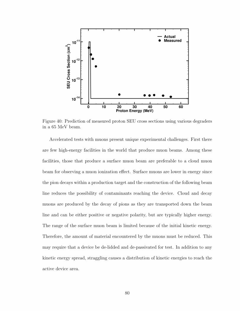
0 10 20 30 40 50 60Proton Energy (MeV)
10-14
10-13
10-12
10-11
SE
U C
ros
s S
ec
tio
n (
cm
2)
ActualMeasured
Figure 40: Prediction of measured proton SEU cross sections using various degradersin a 65 MeV beam.
Accelerated tests with muons present unique experimental challenges. First there
are few high-energy facilities in the world that produce muon beams. Among these
facilities, those that produce a surface muon beam are preferable to a cloud muon
beam for observing a muon ionization effect. Surface muons are lower in energy since
the pion decays within a production target and the construction of the following beam
line reduces the possibility of contaminants reaching the device. Cloud and decay
muons are produced by the decay of pions as they are transported down the beam
line and can be either positive or negative polarity, but are typically higher energy.
The range of the surface muon beam is limited because of the initial kinetic energy.
Therefore, the amount of material encountered by the muons must be reduced. This
may require that a device be de-lidded and de-passivated for test. In addition to any
kinetic energy spread, straggling causes a distribution of kinetic energies to reach the
active device area.
80
Fortunately, if the part is immune to proton direct ionization, there is high confi-
dence that it is also immune to muon direct ionization. Proton testing, unlike that for
muons, is easier and accelerators are more readily available. If the device is sensitive
to proton direct ionization, though, it is possibly also susceptible to muon ionization.
The critical charge of present technologies is less than the muon ionization thresh-
old. It is important to determine when (and if) muons will contribute a significant
portion of the overall error rate. Testing a technology at reduced bias is a leading
indicator for a sensitivity in scaled technologies.
Accelerated tests and soft error rate predictions are standard practices for micro-
electronics applications with high reliability requirements. The data presented here,
however, suggest that the SER of future technologies also may be affected by protons
and muons. Whereas neutrons only rarely interact with nuclei to produce ionizing
particles, both protons and muons are able to generate charge through the electro-
magnetic force. Therefore, the low-energy muon and protons fluxes have the potential
to be a significant component of the SER for sensitive devices.
Our results suggest muon-induced upsets do not affect the soft error rate for 65 nm
and 45 nm SRAMs operated at nominal supply voltage, but they are likely to have
a greater impact for circuits fabricated in smaller process technologies with lower
critical charge values. Ultimately, SRAMs, flip-flops, and combinational logic may
become sensitive to the low-energy muon spectrum. Future error rate predictions
will require characterization of the device LET threshold, consideration of the full
environment, and advanced radiation transport computations.
81
CHAPTER V
RATE PREDICTION ANALYSES
In this Chapter the implications of low-energy proton sensitivity are examined for
various space environments. Although SEU cross sections at proton beam energies
less than 1 MeV have been shown to be more than three orders of magnitude greater
than at higher energies, the operating environment dictates whether this will be a
reliability issue for the part or not. The raw space environments both near or far
from Earth consist heavily of protons. Models to assess the relative importance
of this upset mechanism versus the traditionally dominant particle interactions are
applied to the measured SEU response.
Rate predictions for terrestrial muons are not presented here as the same model
does not indicate significant error rates from muons for this technology generation.
Instead, muon-induced error rates are examined in the following Chapter in a discus-
sion of the implications for future devices.
Traditional Approaches
In the approach provided by Bendel [1], a one parameter fit to the proton upset
cross sections over kinetic energy is derived. The method was intended to capture
elastic recoil events at medium energies near the device upset threshold and inelastic
particle reactions at high energies. Upon the assumption that the probability of an
upset is independent of the proton incident energy for high-energy particle reactions,
the cross section curve should follow exp(−E/200 MeV) according to [92]. Bendel
82
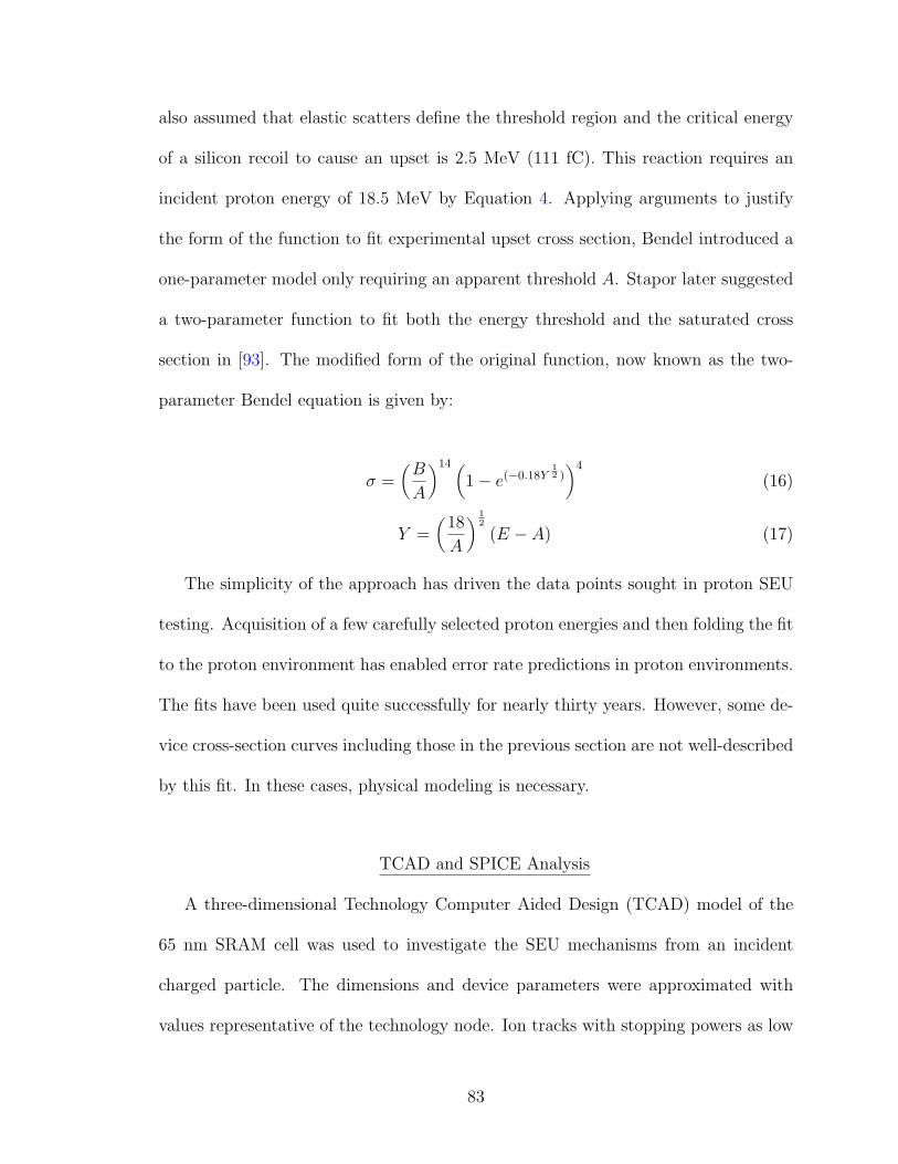
also assumed that elastic scatters define the threshold region and the critical energy
of a silicon recoil to cause an upset is 2.5 MeV (111 fC). This reaction requires an
incident proton energy of 18.5 MeV by Equation 4. Applying arguments to justify
the form of the function to fit experimental upset cross section, Bendel introduced a
one-parameter model only requiring an apparent threshold A. Stapor later suggested
a two-parameter function to fit both the energy threshold and the saturated cross
section in [93]. The modified form of the original function, now known as the two-
parameter Bendel equation is given by:
σ =(B
A
)14 (1− e(−0.18Y
12 ))4
(16)
Y =(
18
A
) 12
(E − A) (17)
The simplicity of the approach has driven the data points sought in proton SEU
testing. Acquisition of a few carefully selected proton energies and then folding the fit
to the proton environment has enabled error rate predictions in proton environments.
The fits have been used quite successfully for nearly thirty years. However, some de-
vice cross-section curves including those in the previous section are not well-described
by this fit. In these cases, physical modeling is necessary.
TCAD and SPICE Analysis
A three-dimensional Technology Computer Aided Design (TCAD) model of the
65 nm SRAM cell was used to investigate the SEU mechanisms from an incident
charged particle. The dimensions and device parameters were approximated with
values representative of the technology node. Ion tracks with stopping powers as low
83
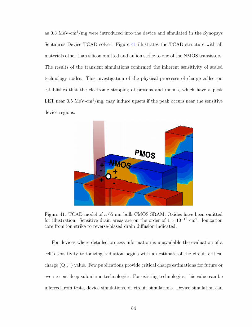
as 0.3 MeV-cm2/mg were introduced into the device and simulated in the Synopsys
Sentaurus Device TCAD solver. Figure 41 illustrates the TCAD structure with all
materials other than silicon omitted and an ion strike to one of the NMOS transistors.
The results of the transient simulations confirmed the inherent sensitivity of scaled
technology nodes. This investigation of the physical processes of charge collection
establishes that the electronic stopping of protons and muons, which have a peak
LET near 0.5 MeV-cm2/mg, may induce upsets if the peak occurs near the sensitive
device regions.
Figure 41: TCAD model of a 65 nm bulk CMOS SRAM. Oxides have been omittedfor illustration. Sensitive drain areas are on the order of 1 × 10⁻¹⁰ cm2. Ionizationcore from ion strike to reverse-biased drain diffusion indicated.
For devices where detailed process information is unavailable the evaluation of a
cell’s sensitivity to ionizing radiation begins with an estimate of the circuit critical
charge (Q crit) value. Few publications provide critical charge estimations for future or
even recent deep-submicron technologies. For existing technologies, this value can be
inferred from tests, device simulations, or circuit simulations. Device simulation can
84

be used to provide an estimate of Q crit, but requires at the least basic knowledge of the
process. If a chip has been fabricated, accelerated testing can be useful to determine
the LET threshold, but the estimation of Q crit still requires the assumption of a
charge collection depth and may require at-angle testing and physical modeling to
validate. Other works have attempted to provide models for pulse shaping for circuit
simulations and critical charge analysis, but often lack any comparison to other forms
of determination.
In our first evaluation of critical charge values, circuit simulations were performed.
Predictive models [94, 95] for various nodes were downloaded from the Predictive
Technology Model website [96]. A standard 6T SRAM cell based on the existing
65 nm design was constructed to establish transistor width to length ratios. For
each smaller technology node, the appropriate MOSFET models were included in the
netlist and the transistor dimensions were scaled by the square root of two. The
voltage supply was also reduced using projections in the ITRS Roadmap [97]. A
current source based on [98] was added to the netlist to perform transient charge
injection. The parameters of the source were varied and the current integrated to
obtain the injected charge. The largest quantity of charge that did not upset the
circuit was recorded as the critical charge. These values are provided in Table 9.
The problems associated with a critical charge estimation from SPICE are the
omission of parasitic capacitances in a predictive circuit netlist and the need for
a current source with accurate pulse shaping. Several works have shown that this
method may provide overestimates simply due to the current pulse shape [99, 100].
Therefore the SPICE values will be taken as an upper bound of the critical charge.
85

One could also base estimates of Q crit on rough calculations of the gate capaci-
tances as described in Chapter I Section . The calculations performed here are based
on the trend in values projected by the ITRS Roadmap. The values are independent
of the particular process and can be used to generalize the industry as a whole. In
the roadmap, the total gate capacitance for a minimum length device is expected to
remain relatively constant at 1 fF/µm over the next several generations. From the
voltage and capacitance on an NMOS and PMOS pair, we derive an estimate of the
Q crit values for 65 through 16 nm technologies. These values are used as a lower
bound for Q crit in our subsequent analysis.
When comparing with the data in Figure 7 the predictions have good agreement to
the extrapolated fit. In fact, Rodbell [32] quotes a critical charge for 65 nm SOI parts
between 0.21 and 0.27 fC and an evaluation of the extrapolated fit yields 0.25 fC.
It should be noted that further extrapolation under-predicts values provided in the
table.
Table 9: Critical Charge EstimatesTechnology (nm) 65 45 32 22 16
Vdd (V) 1.2 1.1 0.97 0.90 0.84Q crit lower (fC) 0.32 0.21 0.13 0.088 0.056Q crit upper (fC) 1.3 0.71 0.44 0.36 0.19
Radiation Transport Modeling
MRED [101] (Monte Carlo Radiative Energy Deposition version 920) was used to
investigate the energy deposition by ions and protons. MRED is based on Geant4 [102]
(currently release 9.4.p01), which comprises reliable and well-calibrated computa-
tional physics models for the transport of radiation through matter. Geant4 is a
86
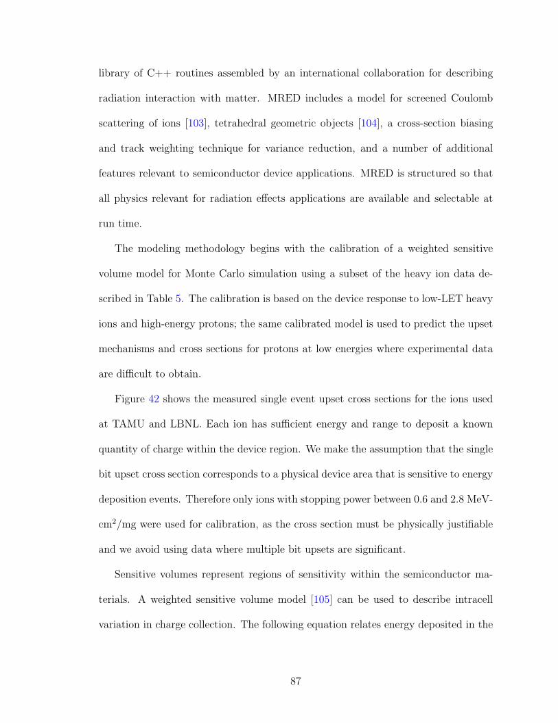
library of C++ routines assembled by an international collaboration for describing
radiation interaction with matter. MRED includes a model for screened Coulomb
scattering of ions [103], tetrahedral geometric objects [104], a cross-section biasing
and track weighting technique for variance reduction, and a number of additional
features relevant to semiconductor device applications. MRED is structured so that
all physics relevant for radiation effects applications are available and selectable at
run time.
The modeling methodology begins with the calibration of a weighted sensitive
volume model for Monte Carlo simulation using a subset of the heavy ion data de-
scribed in Table 5. The calibration is based on the device response to low-LET heavy
ions and high-energy protons; the same calibrated model is used to predict the upset
mechanisms and cross sections for protons at low energies where experimental data
are difficult to obtain.
Figure 42 shows the measured single event upset cross sections for the ions used
at TAMU and LBNL. Each ion has sufficient energy and range to deposit a known
quantity of charge within the device region. We make the assumption that the single
bit upset cross section corresponds to a physical device area that is sensitive to energy
deposition events. Therefore only ions with stopping power between 0.6 and 2.8 MeV-
cm2/mg were used for calibration, as the cross section must be physically justifiable
and we avoid using data where multiple bit upsets are significant.
Sensitive volumes represent regions of sensitivity within the semiconductor ma-
terials. A weighted sensitive volume model [105] can be used to describe intracell
variation in charge collection. The following equation relates energy deposited in the
87
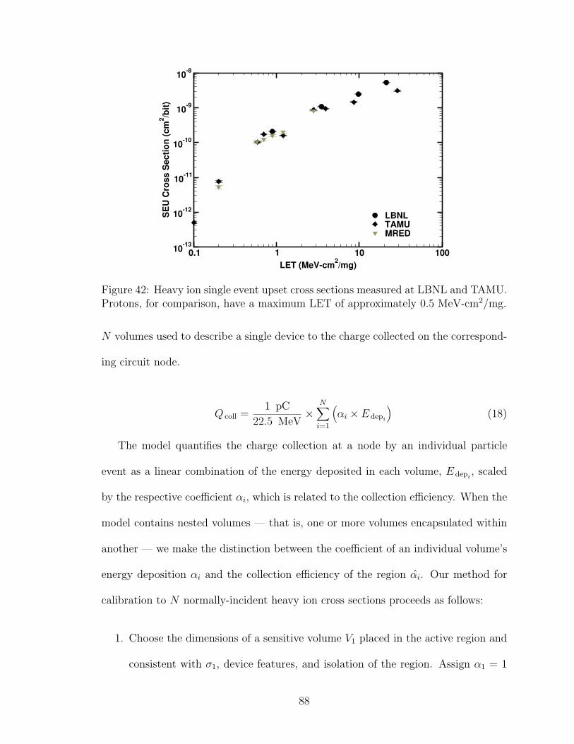
0.1 1 10 100
LET (MeV-cm2/mg)
10-13
10-12
10-11
10-10
10-9
10-8
SE
U C
ross S
ecti
on
(cm
2/b
it)
LBNLTAMUMRED
Figure 42: Heavy ion single event upset cross sections measured at LBNL and TAMU.Protons, for comparison, have a maximum LET of approximately 0.5 MeV-cm2/mg.
N volumes used to describe a single device to the charge collected on the correspond-
ing circuit node.
Q coll =1 pC
22.5 MeV×
N∑i=1
(αi × E depi
)(18)
The model quantifies the charge collection at a node by an individual particle
event as a linear combination of the energy deposited in each volume, E depi, scaled
by the respective coefficient αi, which is related to the collection efficiency. When the
model contains nested volumes — that is, one or more volumes encapsulated within
another — we make the distinction between the coefficient of an individual volume’s
energy deposition αi and the collection efficiency of the region αi. Our method for
calibration to N normally-incident heavy ion cross sections proceeds as follows:
1. Choose the dimensions of a sensitive volume V1 placed in the active region and
consistent with σ1, device features, and isolation of the region. Assign α1 = 1
88

to indicate 100% charge collection in this volume.
2. For each heavy ion cross section calibration value σi, where 1 < i ≤ N and
σi > σi−1, ( or selected points along a Weibull curve ), create a sensitive volume
Vi in the substrate with a surface area equal to σi. Assume the depth, di, of Vi
is the same as the lateral dimension,√σi.
3. Assign each sensitive volume Vi, where i > 1, a charge collection efficiency
αi = Q crit( pC)LETi×di
where LETi is in units of pC/µm and di in µm. This relationship
essentially uses αi to modify the quantity of charge generated in Vi required to
exceed the circuit Q crit (i.e., a strike further from the device requires a particle
with a larger LET to upset the cell than a strike near the device).
4. Create a larger outer volume, with low efficiency, for high-energy proton sec-
ondary particles.
5. Assign αi = αi−∑Nj=i+1 αj, where i > 1, to obtain the coefficients necessary for
Equation 18.
6. Simulate the experimental conditions and adjust parameters until good agree-
ment is achieved with both heavy ion and high-energy proton datasets.
Following this method, we created the model illustrated in Figure 43. Volume V1
was assumed to encompass a transistor bounded in width and depth by shallow trench
isolation and assigned α1 = 1. Volumes V2 and V3 were assigned individual coefficients
0.52 and 0.25 respectively. The outer volume was calibrated to α4 = 0.05 with upset
cross sections from protons with energy greater than 32.5 MeV, corresponding to
nuclear reaction-driven upsets.
89
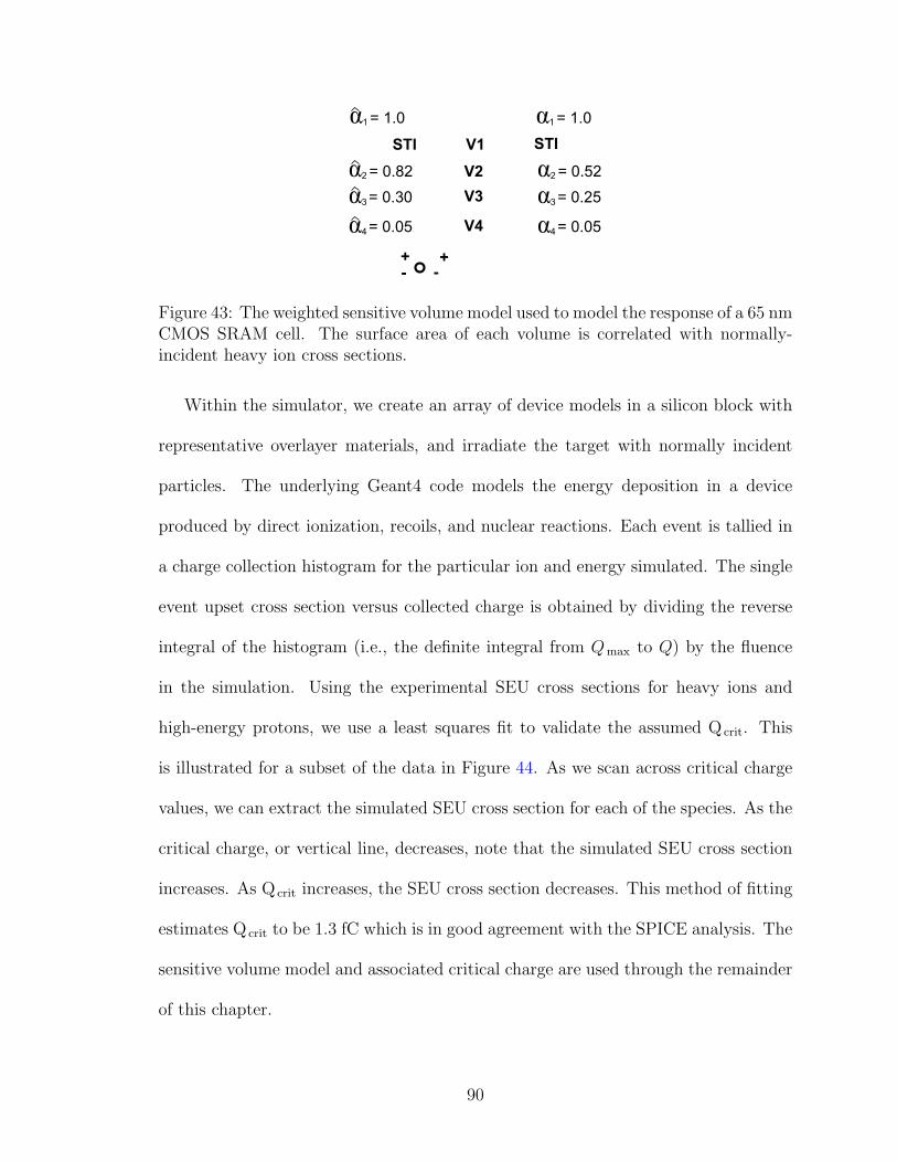
Figure 43: The weighted sensitive volume model used to model the response of a 65 nmCMOS SRAM cell. The surface area of each volume is correlated with normally-incident heavy ion cross sections.
Within the simulator, we create an array of device models in a silicon block with
representative overlayer materials, and irradiate the target with normally incident
particles. The underlying Geant4 code models the energy deposition in a device
produced by direct ionization, recoils, and nuclear reactions. Each event is tallied in
a charge collection histogram for the particular ion and energy simulated. The single
event upset cross section versus collected charge is obtained by dividing the reverse
integral of the histogram (i.e., the definite integral from Qmax to Q) by the fluence
in the simulation. Using the experimental SEU cross sections for heavy ions and
high-energy protons, we use a least squares fit to validate the assumed Q crit. This
is illustrated for a subset of the data in Figure 44. As we scan across critical charge
values, we can extract the simulated SEU cross section for each of the species. As the
critical charge, or vertical line, decreases, note that the simulated SEU cross section
increases. As Q crit increases, the SEU cross section decreases. This method of fitting
estimates Q crit to be 1.3 fC which is in good agreement with the SPICE analysis. The
sensitive volume model and associated critical charge are used through the remainder
of this chapter.
90
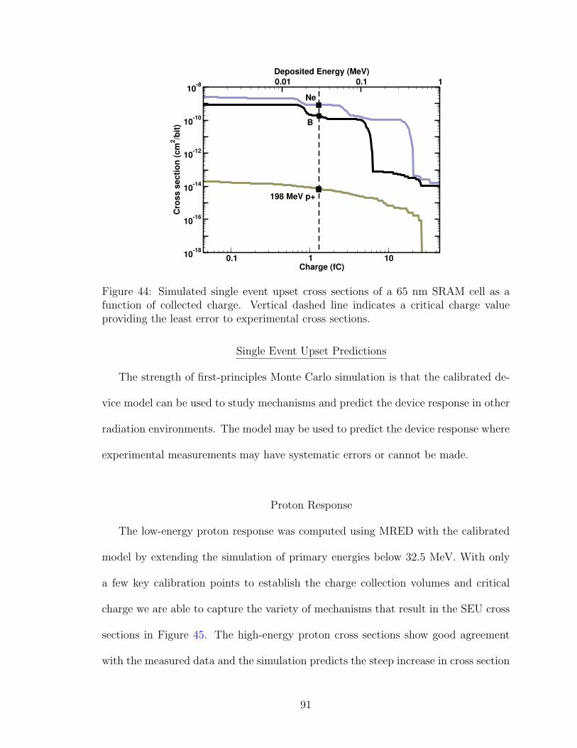
0.01 0.1 1
Deposited Energy (MeV)
10-18
10-16
10-14
10-12
10-10
10-8
Cro
ss
se
cti
on
(c
m2/b
it)
0.1 1 10Charge (fC)
198 MeV p+
B
Ne
Figure 44: Simulated single event upset cross sections of a 65 nm SRAM cell as afunction of collected charge. Vertical dashed line indicates a critical charge valueproviding the least error to experimental cross sections.
Single Event Upset Predictions
The strength of first-principles Monte Carlo simulation is that the calibrated de-
vice model can be used to study mechanisms and predict the device response in other
radiation environments. The model may be used to predict the device response where
experimental measurements may have systematic errors or cannot be made.
Proton Response
The low-energy proton response was computed using MRED with the calibrated
model by extending the simulation of primary energies below 32.5 MeV. With only
a few key calibration points to establish the charge collection volumes and critical
charge we are able to capture the variety of mechanisms that result in the SEU cross
sections in Figure 45. The high-energy proton cross sections show good agreement
with the measured data and the simulation predicts the steep increase in cross section
91

0.1 1 10 100Proton Energy (MeV)
10-16
10-14
10-12
10-10
SE
U C
ros
s S
ec
tio
n (
cm
2/b
it)
GSFCLBNLUC DavisIUMRED
Figure 45: Simulated and experimental proton cross sections of a 65 nm SRAM cell.Model provides good agreement at high energy and captures the steep increase incross section at low energy.
Figure 46: Events causing single event upsets in a 65 nm SRAM cell for 1.4, 4.6,and 32.5 MeV incident protons. The material dimensions have been reduced forillustration purposes.
92
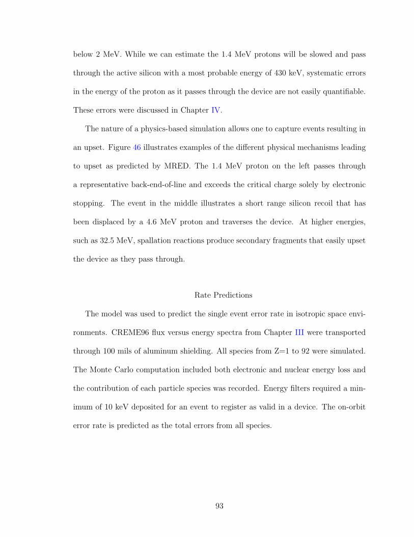
below 2 MeV. While we can estimate the 1.4 MeV protons will be slowed and pass
through the active silicon with a most probable energy of 430 keV, systematic errors
in the energy of the proton as it passes through the device are not easily quantifiable.
These errors were discussed in Chapter IV.
The nature of a physics-based simulation allows one to capture events resulting in
an upset. Figure 46 illustrates examples of the different physical mechanisms leading
to upset as predicted by MRED. The 1.4 MeV proton on the left passes through
a representative back-end-of-line and exceeds the critical charge solely by electronic
stopping. The event in the middle illustrates a short range silicon recoil that has
been displaced by a 4.6 MeV proton and traverses the device. At higher energies,
such as 32.5 MeV, spallation reactions produce secondary fragments that easily upset
the device as they pass through.
Rate Predictions
The model was used to predict the single event error rate in isotropic space envi-
ronments. CREME96 flux versus energy spectra from Chapter III were transported
through 100 mils of aluminum shielding. All species from Z=1 to 92 were simulated.
The Monte Carlo computation included both electronic and nuclear energy loss and
the contribution of each particle species was recorded. Energy filters required a min-
imum of 10 keV deposited for an event to register as valid in a device. The on-orbit
error rate is predicted as the total errors from all species.
93

International Space Station Orbit
Figure 47 shows the predicted error rate in the ISS orbit with 100 mils of aluminum
shielding. Similar to the cross sections, we plot the error rate as a function of charge.
This allows us to see the sensitivity to the critical charge parameter. In this proton-
rich environment, we focus on the proton contribution. Two curves are shown for
the protons. The curve labeled ‘H (dE/dx)’ represents the contribution from proton
direct ionization only, and the second labeled ‘H (all processes)’ includes recoils and
nuclear inelastic events. The vertical dashed line once again marks the critical charge.
The model predicts that direct ionization from protons is a large contributor to the
total error rate, which follows the ‘all processes’ curve. The predicted error rate for
this environment is 4.1× 10⁻⁸ upsets per bit per day.
10-10
10-8
10-6
10-4
Err
or
Ra
te (
bit
-1d
ay
-1)
Total Z=1 to 92
0.1 1 10Critical Charge (fC)
Qcrit
Fe
O
He
H (dE/dx)
H (all processes)
Figure 47: Simulated 65 nm SRAM error rate as a function of critical charge forCREME96 International Space Station orbit, AP8MIN, magnetic quiet, solar mini-mum, with 100 mils of aluminum shielding. Direct ionization from protons contributeheavily to the error rate.
94
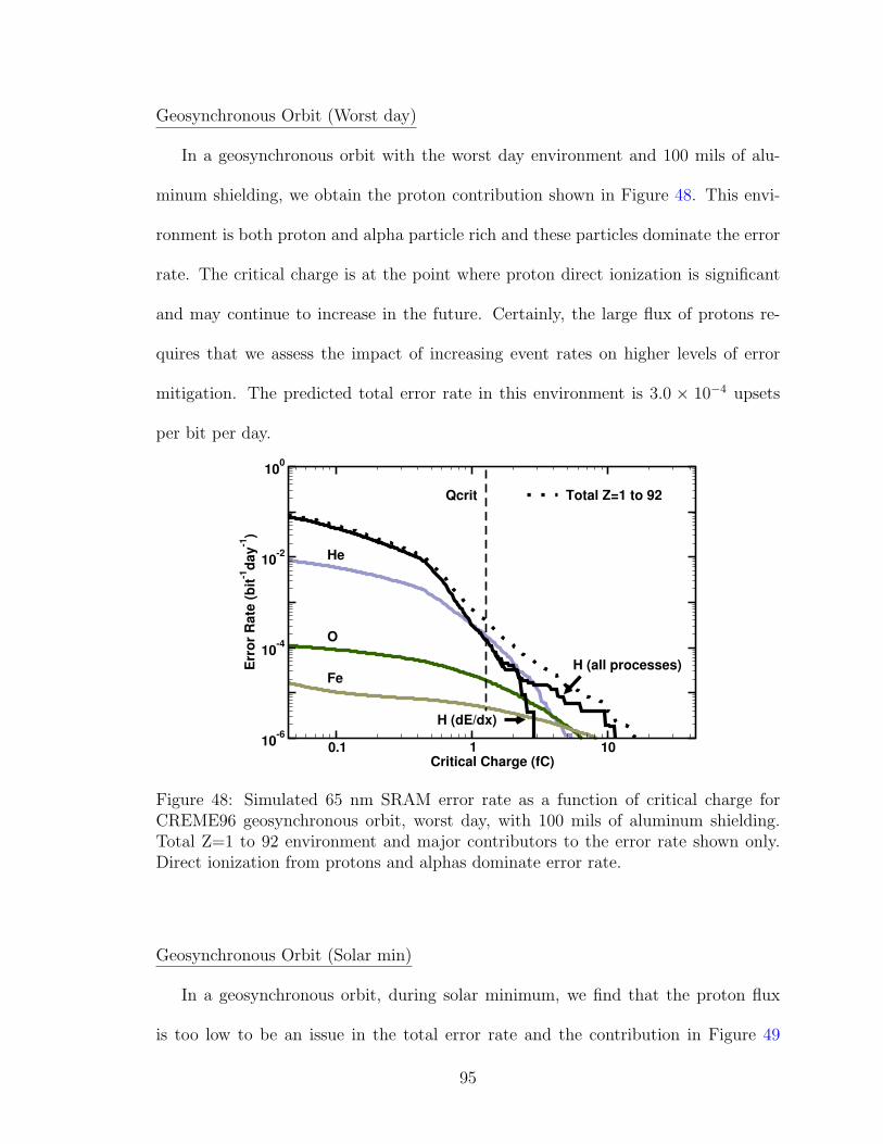
Geosynchronous Orbit (Worst day)
In a geosynchronous orbit with the worst day environment and 100 mils of alu-
minum shielding, we obtain the proton contribution shown in Figure 48. This envi-
ronment is both proton and alpha particle rich and these particles dominate the error
rate. The critical charge is at the point where proton direct ionization is significant
and may continue to increase in the future. Certainly, the large flux of protons re-
quires that we assess the impact of increasing event rates on higher levels of error
mitigation. The predicted total error rate in this environment is 3.0 × 10⁻⁴ upsets
per bit per day.
10-6
10-4
10-2
100
Err
or
Ra
te (
bit
-1d
ay
-1)
Total Z=1 to 92
0.1 1 10Critical Charge (fC)
Qcrit
He
O
FeH (all processes)
H (dE/dx)
Figure 48: Simulated 65 nm SRAM error rate as a function of critical charge forCREME96 geosynchronous orbit, worst day, with 100 mils of aluminum shielding.Total Z=1 to 92 environment and major contributors to the error rate shown only.Direct ionization from protons and alphas dominate error rate.
Geosynchronous Orbit (Solar min)
In a geosynchronous orbit, during solar minimum, we find that the proton flux
is too low to be an issue in the total error rate and the contribution in Figure 49
95
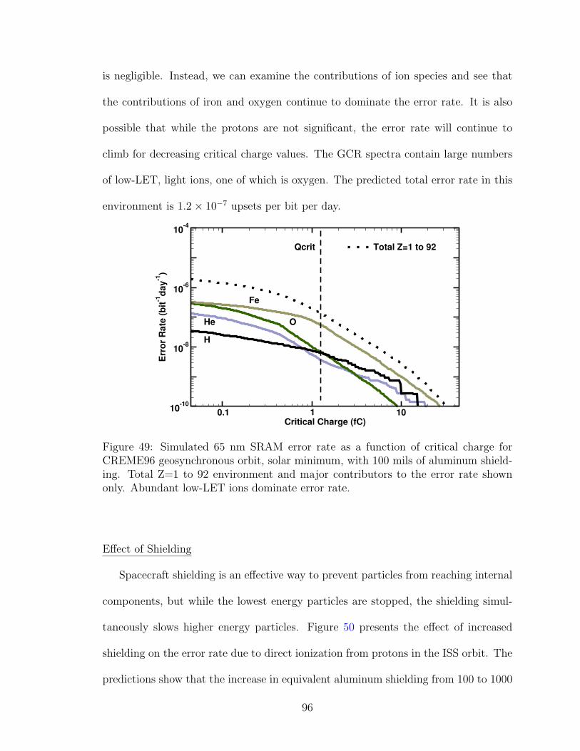
is negligible. Instead, we can examine the contributions of ion species and see that
the contributions of iron and oxygen continue to dominate the error rate. It is also
possible that while the protons are not significant, the error rate will continue to
climb for decreasing critical charge values. The GCR spectra contain large numbers
of low-LET, light ions, one of which is oxygen. The predicted total error rate in this
environment is 1.2× 10⁻⁷ upsets per bit per day.
10-10
10-8
10-6
10-4
Err
or
Ra
te (
bit
-1d
ay
-1)
0.1 1 10Critical Charge (fC)
Qcrit Total Z=1 to 92
H
Fe
OHe
Figure 49: Simulated 65 nm SRAM error rate as a function of critical charge forCREME96 geosynchronous orbit, solar minimum, with 100 mils of aluminum shield-ing. Total Z=1 to 92 environment and major contributors to the error rate shownonly. Abundant low-LET ions dominate error rate.
Effect of Shielding
Spacecraft shielding is an effective way to prevent particles from reaching internal
components, but while the lowest energy particles are stopped, the shielding simul-
taneously slows higher energy particles. Figure 50 presents the effect of increased
shielding on the error rate due to direct ionization from protons in the ISS orbit. The
predictions show that the increase in equivalent aluminum shielding from 100 to 1000
96

mils reduces the rate by 5X, but does not eliminate upsets from low-energy protons.
For other external environments, the level of mitigation gained with shielding will be
dependent on the proton energy spectrum. Therefore, this upset mechanism may still
have a significant contribution to the total error rate in a proton-rich environment,
even behind heavy shielding.
10-10
10-8
10-6
10-4
Err
or
Ra
te (
bit
-1d
ay
-1)
0.1 1 10Critical Charge (fC)
Qcrit100 mils
400 mils
1000 mils
Figure 50: Simulated 65 nm SRAM error rate due to direct ionization from pro-tons as a function of critical charge for CREME96 International Space Station orbit,AP8MIN, magnetic quiet, solar minimum, with 100, 400, and 1000 mils of aluminumshielding.
Conclusions
Traditional models for evaluating the effects of protons on devices considered
for space applications have only considered the nuclear interactions caused by this
substantial portion of the environment. The distinction between direct ionization and
nuclear-reaction induced effects has led to the development and application of different
tools to evaluate each independently as if the environment could be separated into
97
these two constituents. With the onset of proton direct ionization upsets, physics-
based Monte Carlo models work quite well to evaluate single events.
We have found that it is possible to describe the charge collection of a memory cell
under heavy ion and proton irradiation by a weighted sensitive volume model. The
specific model described for a 65 nm bulk CMOS process reproduced the SEU cross
section over LET and also matched the proton cross sections over beam energy. When
the model was evaluated under the proton-rich space environments, the error rates due
to proton direct ionization alone were comparable to the nuclear-reaction component.
Similar simulations for this technology in the terrestrial environment showed negligible
effects from protons and muons compared to typical neutron-induced error rates.
98
CHAPTER VI
IMPLICATIONS FOR FUTURE DEVICES
According to the ITRS roadmap, conventional bulk planar CMOS will have diffi-
culty continuing to meet the needs of the industry beyond gate lengths of 16 nm. It
has been proposed that ultrathin body silicon-on-insulator or multiple gate technolo-
gies will be required to fill the need. The semiconductor industry is in the process
of transitioning some applications to these new technologies. Even in light of the
introduction of the new processes, conventional bulk planar CMOS may see several
more generations of use.
Predictions for soft error rates at scaled technologies nodes beyond one generation
out have no shortage of challenges. Even in bulk planar technologies, the initial spa-
tial distributions of energy deposition, charge collection by contacts with nanometer
dimensions, charge diffusion, and lack of calibration data make the application of
a predictive model suspect. Further, the uncertainty in the industry’s roadmap for
technologies clouds our ability to look into the future.
In this section, the implications of various processes on the proton and muon error
rates are examined. The differences in these analyses concern the charge collection
due to geometrical changes. Other factors related to the specific technology are not
considered and remain as future work when these technologies become available.
At deep-submicron technology nodes, it is likely that the sensitive volume for
charge collection does not scale proportionally with the technology feature size. In
the original works that developed the concept of a sensitive volume, the dominant
99
mechanism for charge collection was drift in the depletion region around the junction.
For large devices, circa 1990, this volume may have scaled well with the junction size.
However, diffusion of charge to devices with nanometer dimensions is an important
consideration. Thus diffusion transport may establish the dimensions of the sensitive
volume. It is probably the case that more complicated sensitive volume models would
provide a better description of the amount of charge seen at the circuit node. However,
in the absence of SEU cross section data and the complications of capturing multiple
node charge collection and multiple cell upsets across technology nodes, we will forgo
this model. Instead, the choice of a single sensitive volume will be used as an indicator
for the trend in the soft error rates.
Larger diffusion areas would cause the generated charge curves to translate to
high error rates. An increase in the sensitive volume depth will also increase charge
collection for any given particle’s linear energy transfer through an increase in path-
length. In this case the energy deposition curves would translate to the right causing
the soft error rates for an assumed Q crit to increase.
The analysis is performed with MRED similarly to our previously presented model
and simulations. However, in this work we have chosen to use a single sensitive volume
model for each SRAM cell. The sensitive volume simply reports the amount of energy
deposited within its boundaries for each particle event. The simple approximation of
the model is that a cell upset occurs if the deposited charge is greater than or equal to
the critical charge. In Section V we have discussed use of multiple weighted sensitive
volume models.
Despite these pitfalls, for each technology node investigated, an array of volumes
was constructed to represent a small group of SRAM cells. An individual sensitive
100
volume was sized according to the projected NMOS gate and drain geometry. As
mentioned, the correlation of the volume lateral dimensions with the gate length is
one possible, but not necessarily the correct, approximation of the effects of technology
scaling on charge collection. For the simplicity of analysis, we will make the previous
assumption for all technologies. To translate the model between technology nodes,
the lateral dimensions of the model were scaled by λ =√
2, as well as the spacing
between volumes.
A multilayer planar stack structure was used to model the substrate and back-
end-of-line materials for radiation transport. The layers were constructed of several
layers of common microelectronics materials such as silicon, SiO2, and copper. On
top of the overlayers, 200 µm of silicon was added to slow the lowest energy particles
in the environment model to stopping. The exact details of the composition have very
little effect on the results as the primary energy loss mechanism involved is electronic
stopping. The material structure was reused for all technologies and did not change
with scaling. The sensitive volume models were placed within the substrate layer.
The simulations produce histograms of energy deposition events weighted appro-
priately by the input flux spectrum. The simulation data are integrated and scaled
to present plots of soft error rate versus the charge generated in the cell. The thick
curves represent the range of Q crit values that fall between our established upper and
lower bounds for the technology node.
101
Charge Collection Models
Additionally, Monte Carlo physics-based radiation transport simulations of the
terrestrial muon spectrum were performed. The sensitive volumes were scaled later-
ally according to the representative technologies and the energy deposited by each
particle was recorded.
In bulk planar CMOS, we note that there is little motivation for decreasing the
well depth in the same way that scaling drives packing density. Therefore we as-
sume a constant collection depth of 0.5 µm. We will discuss the implications of our
assumptions later.
FinFETs have been proposed as process technology to replace conventional bulk
planar CMOS. The introduction of the fin structure allows for better control of the
transistor channel but could also change the nature of the charge collection from a
single event.
To establish a reasonable charge collection depth for bulk FinFETS, we have per-
formed 3D drift-diffusion simulations with the Synopsys Sentaurus device simulator
following a single event strike to a reverse-biased n+ junction in a silicon fin represen-
tative of a 22 nm device (Figure 51). The fin height (FH) was assumed to be 170 nm
and the fin width (FW) 25 nm. The fin was placed on top of a 2×2×2 µm substrate
volume and a potential of 1 V was applied to the n+ diffusion and Nwells. The par-
ticle struck the fin at normal incidence with an LET of 0.5 MeV-cm2/mg. The track
extended 1.5 µm into the substrate from the top of the fin and had a characteristic
radius of 2 nm.
The transient simulations solve for the current through the drain contact as shown
in Figure 52. The integrated current is also plotted as an indication of the charge
102
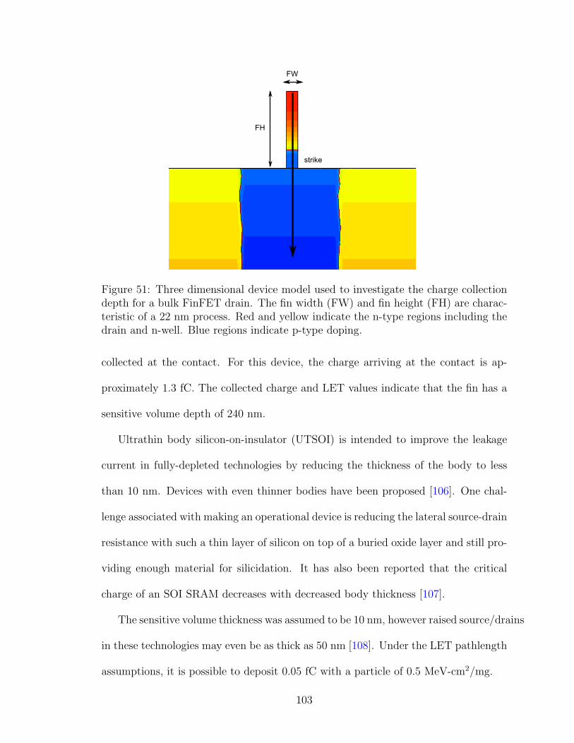
Figure 51: Three dimensional device model used to investigate the charge collectiondepth for a bulk FinFET drain. The fin width (FW) and fin height (FH) are charac-teristic of a 22 nm process. Red and yellow indicate the n-type regions including thedrain and n-well. Blue regions indicate p-type doping.
collected at the contact. For this device, the charge arriving at the contact is ap-
proximately 1.3 fC. The collected charge and LET values indicate that the fin has a
sensitive volume depth of 240 nm.
Ultrathin body silicon-on-insulator (UTSOI) is intended to improve the leakage
current in fully-depleted technologies by reducing the thickness of the body to less
than 10 nm. Devices with even thinner bodies have been proposed [106]. One chal-
lenge associated with making an operational device is reducing the lateral source-drain
resistance with such a thin layer of silicon on top of a buried oxide layer and still pro-
viding enough material for silicidation. It has also been reported that the critical
charge of an SOI SRAM decreases with decreased body thickness [107].
The sensitive volume thickness was assumed to be 10 nm, however raised source/drains
in these technologies may even be as thick as 50 nm [108]. Under the LET pathlength
assumptions, it is possible to deposit 0.05 fC with a particle of 0.5 MeV-cm2/mg.
103

0
20
40
60
80
Dra
in C
urr
en
t (u
A)
0 20 40 60 80Time (psec)
0
0.5
1
1.5
2
Co
lle
cte
d C
ha
rge
(fC
)
Figure 52: Device simulation results for single event strike into fin indicating draincurrent and collected charge.
The contacting scheme, which has been ignored here will also affect the sensitive
volume. As discussed in [109], individual contacts to source/drain regions in multi-fin
devices are unlikely. Additionally, bar contacts across the fins add parasitic capac-
itance. Instead methods of selective epitaxial growth are preferred. Unless these
regions are completely consumed by silicidation, they could also contribute to the
charge collected following a single event strike.
On-Orbit Single Event Upsets
The particle gun for the proton analysis used the Worst Day flux transported
through 100 mils. This environment was chosen based on the response seen in Sec-
tion V. To isolate the effect of direct ionization only, the nuclear models and recoils
were turned off.
The curves in Figures 53, 54, and 55 show the results of the simulations represent-
ing the cells in the 32, 22, and 16 nm nodes. In each figure, error rates are presented
104
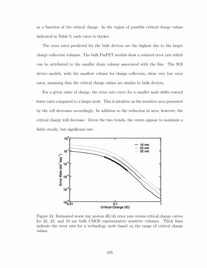
as a function of the critical charge. In the region of possible critical charge values
indicated in Table 9, each curve is thicker.
The error rates predicted for the bulk devices are the highest due to the larger
charge collection volumes. The bulk FinFET models show a reduced error rate which
can be attributed to the smaller drain volume associated with the fins. The SOI
device models, with the smallest volume for charge collection, show very low error
rates, assuming that the critical charge values are similar to bulk devices.
For a given value of charge, the error rate curve for a smaller node shifts toward
lower rates compared to a larger node. This is intuitive as the sensitive area presented
by the cell decreases accordingly. In addition to the reduction in area, however, the
critical charge will decrease. Given the two trends, the errors appear to maintain a
fairly steady, but significant rate.
0.01 0.1 1Critical Charge (fC)
10-5
10-4
10-3
10-2
10-1
100
Err
or
Ra
te (
bit
-1d
ay
-1)
16 nm22 nm32 nm
Figure 53: Estimated worst day proton dE/dx error rate versus critical charge curvesfor 32, 22, and 16 nm bulk CMOS representative sensitive volumes. Thick linesindicate the error rate for a technology node based on the range of critical chargevalues.
105
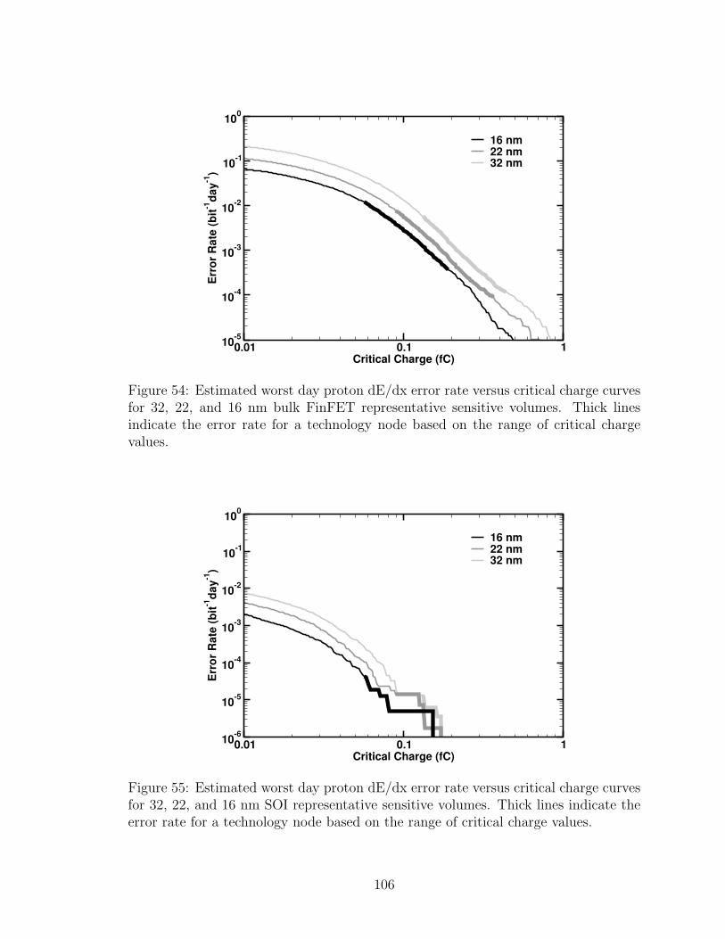
0.01 0.1 1Critical Charge (fC)
10-5
10-4
10-3
10-2
10-1
100
Err
or
Ra
te (
bit
-1d
ay
-1)
16 nm22 nm32 nm
Figure 54: Estimated worst day proton dE/dx error rate versus critical charge curvesfor 32, 22, and 16 nm bulk FinFET representative sensitive volumes. Thick linesindicate the error rate for a technology node based on the range of critical chargevalues.
0.01 0.1 1Critical Charge (fC)
10-6
10-5
10-4
10-3
10-2
10-1
100
Err
or
Ra
te (
bit
-1d
ay
-1)
16 nm22 nm32 nm
Figure 55: Estimated worst day proton dE/dx error rate versus critical charge curvesfor 32, 22, and 16 nm SOI representative sensitive volumes. Thick lines indicate theerror rate for a technology node based on the range of critical charge values.
106
Terrestrial Single Event Upsets
Our preliminary estimates indicate that the muon-induced error rates for the 65,
55, 45, and 40 nm technology nodes are insignificant. In all cases, the muon-induced
FIT rate is much lower than those commonly quoted from neutron events which are
typically a few hundred FIT/Mbit. Although it has been shown experimentally that
these nodes are sensitive to direct ionization from muons, the flux of muons with
sufficient stopping power to upset a cell is quite low.
We build on the assumptions laid out for the scaling of sensitive volumes with
technology nodes to examine if and when such a muon susceptibility would become
a reliability issue. For smaller and more sensitive technologies, the flux of muons
that are capable of exceeding a cell’s critical charge value is larger. Consequently, the
muon-induced soft error rate will increase.
The particle gun used the proton, µ+, and µ− spectra obtained from EXPACS
as described in Chapter III. The spectra include the flux of particles greater than
1 MeV.
The estimated muon sea level error rates are shown in Figures 56, 60, and 58 for
32, 22, and 16 nm representative sensitive volumes. Estimated proton error rates
are shown in Figures 57, 59, and 61. Both sets of plots demonstrate similar charac-
teristics. Each curve increases for lower values of critical charge in accordance with
the expectation that a more sensitive device will have a higher error rate. Below the
32 nm technology node, the critical charge has decreased enough that this threshold
now permits a significant rate of errors to occur. For a given process technology it is
also apparent that the surface area of the volume is equally important as the upset
threshold in determining the error rate.
107
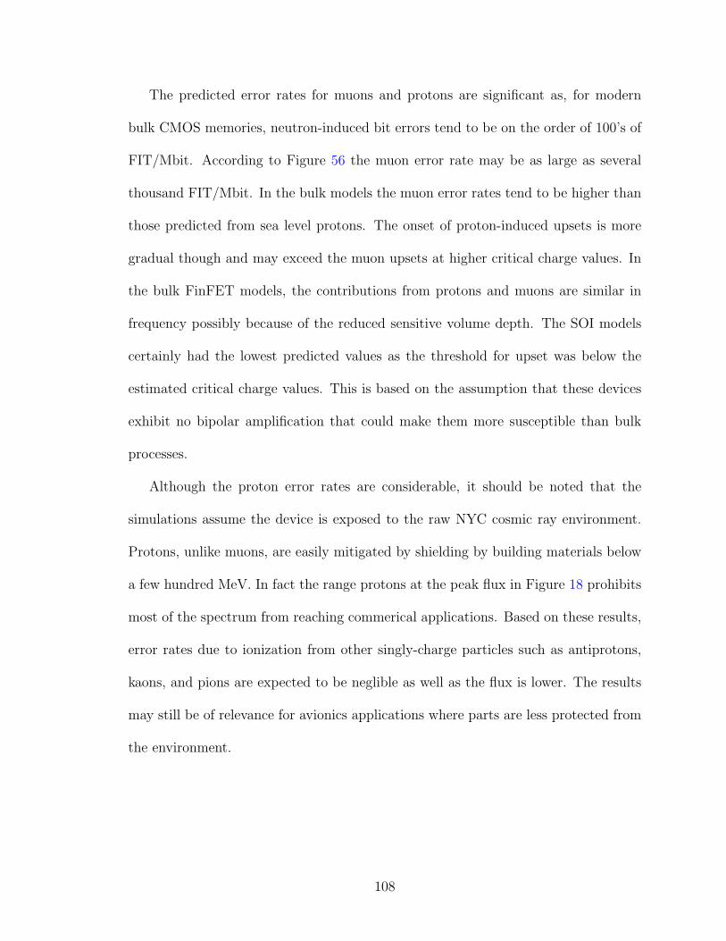
The predicted error rates for muons and protons are significant as, for modern
bulk CMOS memories, neutron-induced bit errors tend to be on the order of 100’s of
FIT/Mbit. According to Figure 56 the muon error rate may be as large as several
thousand FIT/Mbit. In the bulk models the muon error rates tend to be higher than
those predicted from sea level protons. The onset of proton-induced upsets is more
gradual though and may exceed the muon upsets at higher critical charge values. In
the bulk FinFET models, the contributions from protons and muons are similar in
frequency possibly because of the reduced sensitive volume depth. The SOI models
certainly had the lowest predicted values as the threshold for upset was below the
estimated critical charge values. This is based on the assumption that these devices
exhibit no bipolar amplification that could make them more susceptible than bulk
processes.
Although the proton error rates are considerable, it should be noted that the
simulations assume the device is exposed to the raw NYC cosmic ray environment.
Protons, unlike muons, are easily mitigated by shielding by building materials below
a few hundred MeV. In fact the range protons at the peak flux in Figure 18 prohibits
most of the spectrum from reaching commerical applications. Based on these results,
error rates due to ionization from other singly-charge particles such as antiprotons,
kaons, and pions are expected to be neglible as well as the flux is lower. The results
may still be of relevance for avionics applications where parts are less protected from
the environment.
108

0.01 0.1 1Critical Charge (fC)
101
102
103
104
105
106
Mu
on
Err
or
Ra
te (
FIT
/Mb
it)
16nm22nm32nm
Figure 56: Estimated NYC muon-induced error rate versus critical charge curves for32, 22, and 16 nm bulk CMOS representative sensitive volumes. Thick lines indicatethe error rate for a technology node based on the range of critical charge values.
0.01 0.1 1Critical Charge (fC)
101
102
103
104
105
106
Pro
ton
Err
or
Ra
te (
FIT
/Mb
it)
16 nm22 nm32 nm
Figure 57: Estimated NYC proton-induced error rate versus critical charge curves for32, 22, and 16 nm bulk CMOS representative sensitive volumes. Thick lines indicatethe error rate for a technology node based on the range of critical charge values.
109
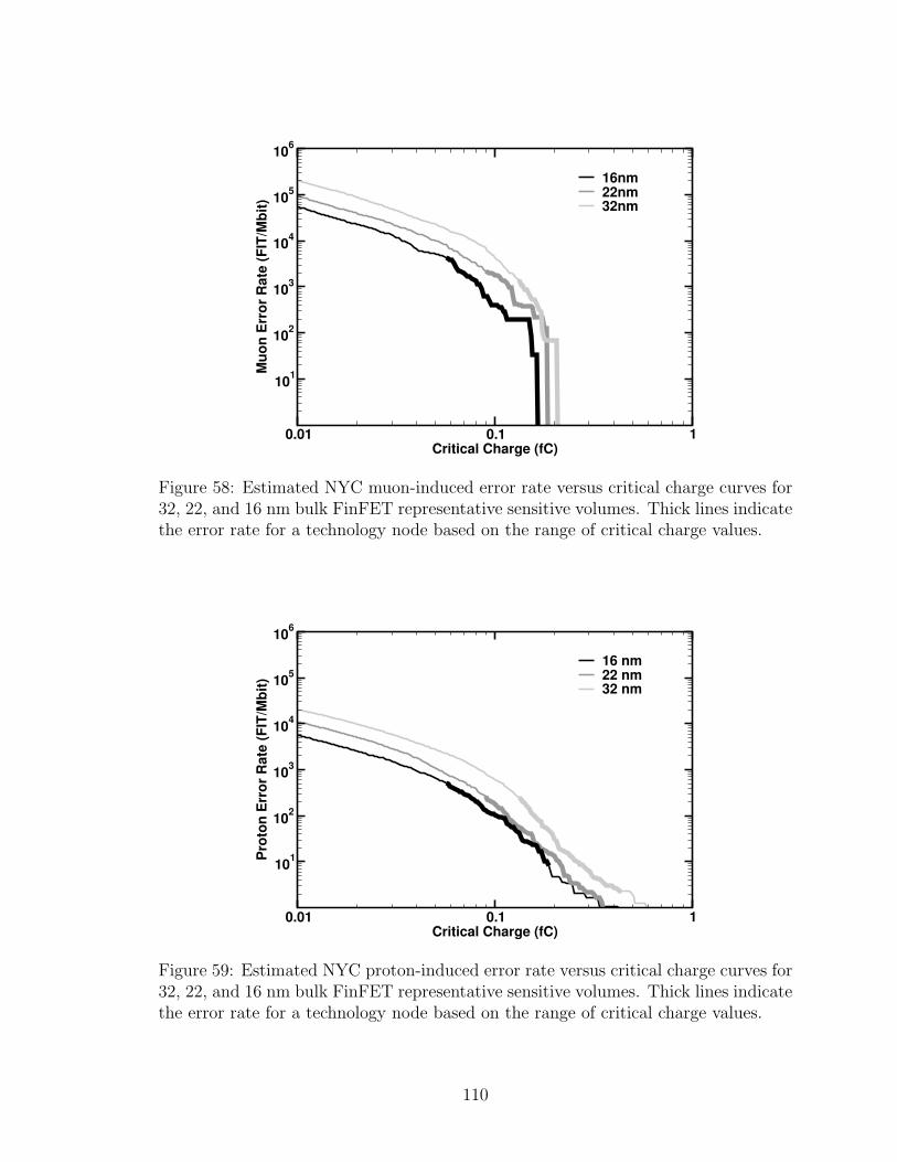
0.01 0.1 1Critical Charge (fC)
101
102
103
104
105
106
Mu
on
Err
or
Ra
te (
FIT
/Mb
it)
16nm22nm32nm
Figure 58: Estimated NYC muon-induced error rate versus critical charge curves for32, 22, and 16 nm bulk FinFET representative sensitive volumes. Thick lines indicatethe error rate for a technology node based on the range of critical charge values.
0.01 0.1 1Critical Charge (fC)
101
102
103
104
105
106
Pro
ton
Err
or
Ra
te (
FIT
/Mb
it)
16 nm22 nm32 nm
Figure 59: Estimated NYC proton-induced error rate versus critical charge curves for32, 22, and 16 nm bulk FinFET representative sensitive volumes. Thick lines indicatethe error rate for a technology node based on the range of critical charge values.
110
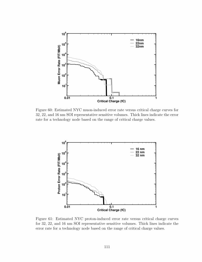
0.01 0.1 1Critical Charge (fC)
101
102
103
104
105
106
Mu
on
Err
or
Ra
te (
FIT
/Mb
it)
16nm22nm32nm
Figure 60: Estimated NYC muon-induced error rate versus critical charge curves for32, 22, and 16 nm SOI representative sensitive volumes. Thick lines indicate the errorrate for a technology node based on the range of critical charge values.
0.01 0.1 1Critical Charge (fC)
101
102
103
104
105
106
Pro
ton
Err
or
Ra
te (
FIT
/Mb
it)
16 nm22 nm32 nm
Figure 61: Estimated NYC proton-induced error rate versus critical charge curvesfor 32, 22, and 16 nm SOI representative sensitive volumes. Thick lines indicate theerror rate for a technology node based on the range of critical charge values.
111
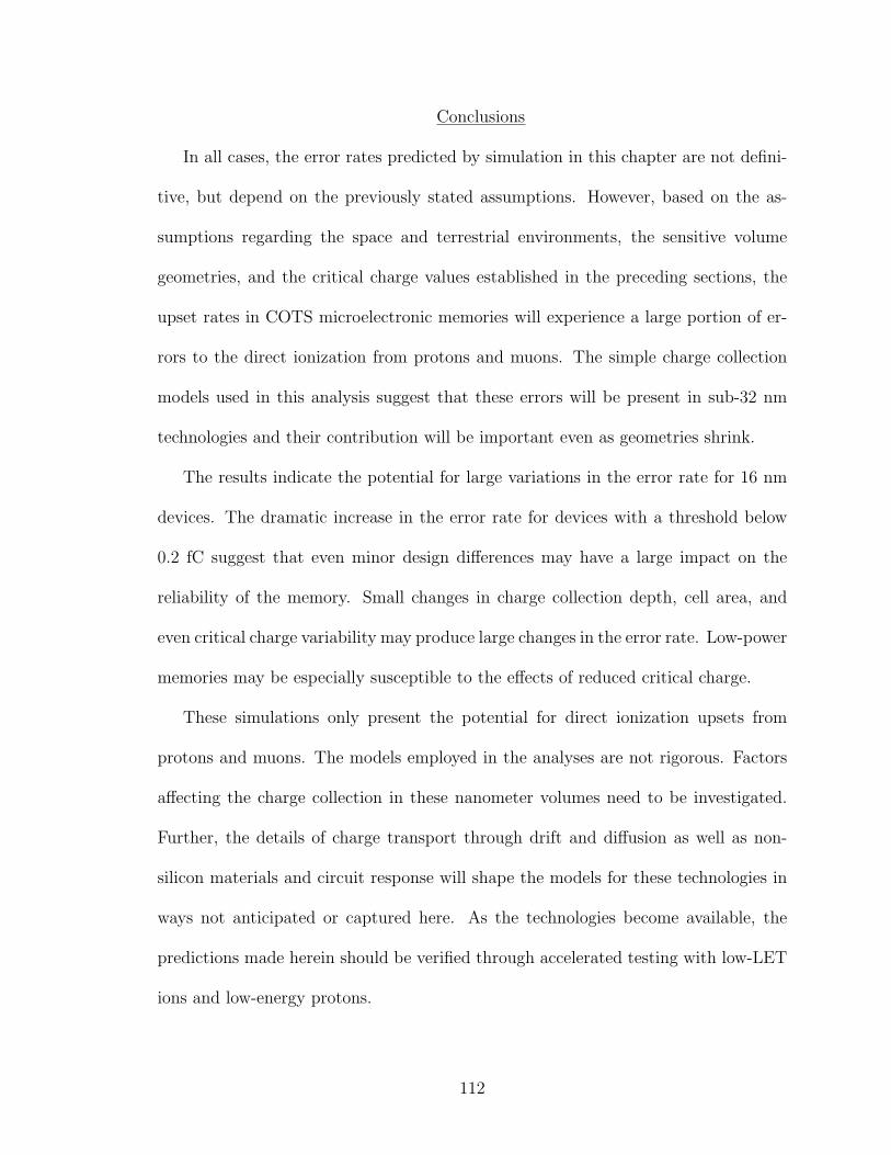
Conclusions
In all cases, the error rates predicted by simulation in this chapter are not defini-
tive, but depend on the previously stated assumptions. However, based on the as-
sumptions regarding the space and terrestrial environments, the sensitive volume
geometries, and the critical charge values established in the preceding sections, the
upset rates in COTS microelectronic memories will experience a large portion of er-
rors to the direct ionization from protons and muons. The simple charge collection
models used in this analysis suggest that these errors will be present in sub-32 nm
technologies and their contribution will be important even as geometries shrink.
The results indicate the potential for large variations in the error rate for 16 nm
devices. The dramatic increase in the error rate for devices with a threshold below
0.2 fC suggest that even minor design differences may have a large impact on the
reliability of the memory. Small changes in charge collection depth, cell area, and
even critical charge variability may produce large changes in the error rate. Low-power
memories may be especially susceptible to the effects of reduced critical charge.
These simulations only present the potential for direct ionization upsets from
protons and muons. The models employed in the analyses are not rigorous. Factors
affecting the charge collection in these nanometer volumes need to be investigated.
Further, the details of charge transport through drift and diffusion as well as non-
silicon materials and circuit response will shape the models for these technologies in
ways not anticipated or captured here. As the technologies become available, the
predictions made herein should be verified through accelerated testing with low-LET
ions and low-energy protons.
112
CHAPTER VII
CONCLUSIONS
The expectation that microelectronics will operate reliability requires the antici-
pation and mitigation of radiation effects. It was proposed in this body of research
that single event upsets in deep-submicron memories will be caused by direct ion-
ization from singly-charged particles. It has been speculated since the industry was
still in its infancy that these particles would exhibit an effect in sufficiently sensitive
devices. However, devices which have been manufactured until the present time have
not seen these effects.
In this work we have shown experimentally that the single event upset cross section
for low-energy protons in 65 nm and smaller bulk CMOS technologies are sufficiently
large to make ionization a substantial upset mechanism in a proton-rich space envi-
ronment. Additionally, these technologies have been experimentally shown to upset
due to muon ionization. The method and facilities used to collect the data not only
show that a proton sensitivity exists in the technologies tested but also provide single
event cross sections that can be used in modeling and rate prediction techniques.
Experimental techniques need to be further developed to obtain similar datasets for
muons.
The continued development of test methods in this area is necessary to confidently
measure and predict the true effects. A number of uncertainties are introduced with
these types of tests ranging from material effects to beam characteristics. Further, the
low-energy environment is not completely characterized and highly-variable. A better
113
understanding of the environment and its extremes will help with reliable predictions.
Through a physics-based modeling approach that utilizes Monte Carlo methods,
the single event effects were shown to have relevance to error rates in proton-rich
space environments and in the terrestrial environment although at smaller technolo-
gies. Continued decreases in critical charges coupled with larger contributions from
singly-charged particles in all natural environments will drive higher error rates in
future technologies. This driver is only offset by accompanying changes in the charge
collection volume, particularly the depth.
A general recommendation can be made based on the outcome of this work. Typi-
cally, in the course of qualifying a part for space or simply quantifying its error rate in
a terrestrial environment, the part will be taken to a proton facility for testing with
energies from tens to hundreds of MeV. This is necessary according to good prac-
tice for space and can also be used as a substitute for monochromatic neutrons for
commercial applications. The data and simulations in this work support the recom-
mendation that the cyclotron beam additionally be degraded and used for low-energy
proton testing. While not providing usable cross sections, this experiment can be
a gating condition for further tests. Datasets which demonstrate a clear roll off in
the proton SEU cross section at energies well above a few MeV strongly suggest the
part is immune to proton direct ionization. If no roll off in the SEU cross section
exists and even increases near stopping or if the result of the degraded beam test is
inconclusive as to demonstrate direct ionization, further testing with an electrostatic
accelerator is recommended.
Low-energy tests with an electrostatic accelerator are much better controlled and
provide data which may be used to calibrate an SEU model for rate predictions. In
114
the case of terrestrial applications, a demonstration of a low-energy proton sensitivity
is a necessary, but not sufficient indication of a low-energy muon sensitivity. In this
case, characterization of the part at a surface muon facility may be pursued.
115

APPENDIX A: EXPACS GENERATED FLUX SPECTRA
Table 10: Positive Muon Flux at Sea Level in NYC
Energy (MeV) Flux (µ+/cm2-s-MeV)
1.1295 5.63403E-08
1.4219 7.09374E-08
1.7901 8.92315E-08
2.2536 1.121E-07
2.8371 1.40606E-07
3.5717 1.76017E-07
4.4965 2.19808E-07
5.6607 2.73664E-07
7.1264 3.39454E-07
8.9716 4.19147E-07
11.295 5.14712E-07
14.219 6.27821E-07
17.901 7.59761E-07
22.536 9.10846E-07
28.371 1.08018E-06
35.717 1.26524E-06
44.965 1.46164E-06
56.607 1.66317E-06
71.264 1.86219E-06
89.716 2.05026E-06
112.95 2.21909E-06
142.19 2.36131E-06
179.01 2.47127E-06
225.36 2.54501E-06
283.71 2.58021E-06
357.17 2.5757E-06
449.65 2.53103E-06
566.07 2.44624E-06
712.64 2.32193E-06
897.16 2.1597E-06
1129.5 1.96276E-06
1421.9 1.73689E-06
116

Energy (MeV) Flux (µ+/cm2-s-MeV)
1790.1 1.49055E-06
2253.6 1.2352E-06
2837.1 9.84129E-07
3571.7 7.50784E-07
4496.5 5.46536E-07
5660.7 3.78675E-07
7126.4 2.49382E-07
8971.6 1.56109E-07
11295 9.3006E-08
14219 5.2888E-08
17901 2.87983E-08
22536 1.50818E-08
28371 7.63068E-09
35717 3.74687E-09
44965 1.79342E-09
56607 8.40168E-10
71264 3.86601E-10
89716 1.7529E-10
117
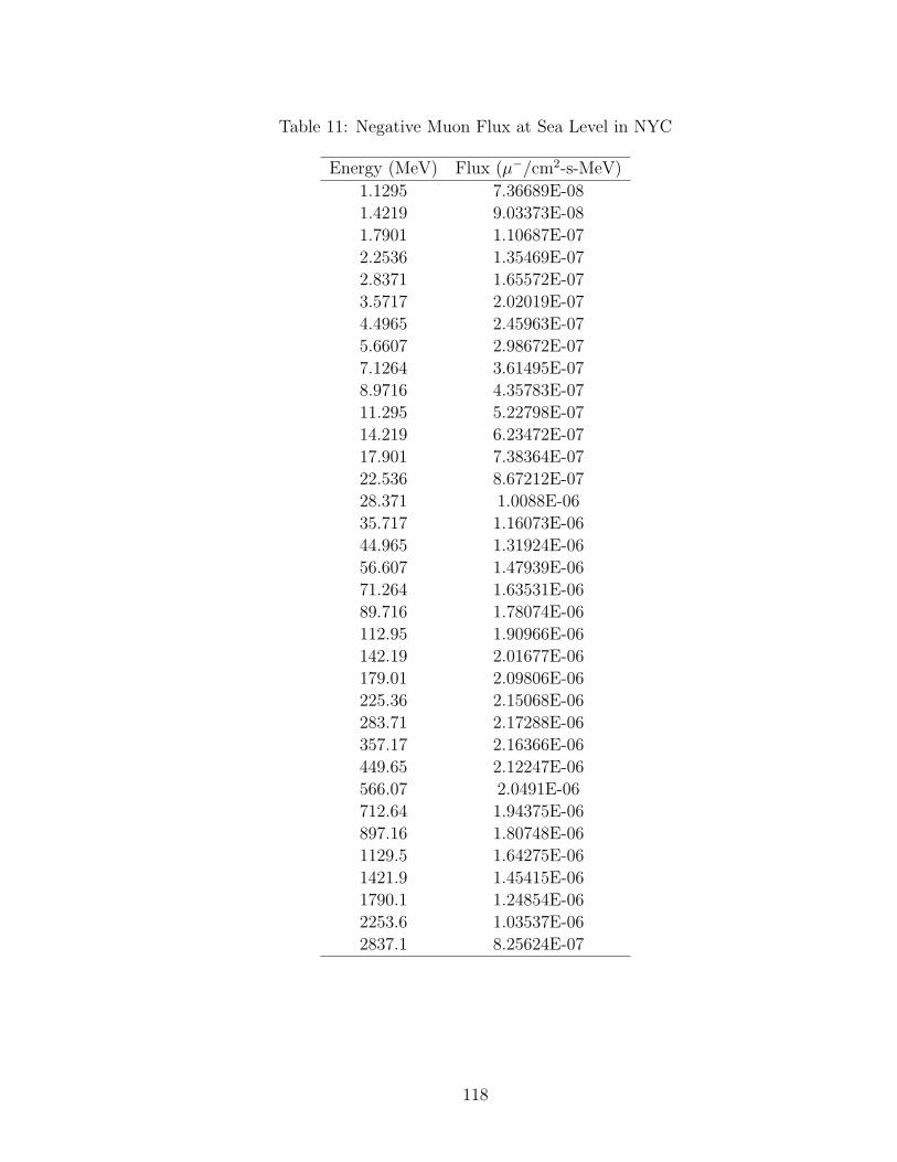
Table 11: Negative Muon Flux at Sea Level in NYC
Energy (MeV) Flux (µ−/cm2-s-MeV)
1.1295 7.36689E-08
1.4219 9.03373E-08
1.7901 1.10687E-07
2.2536 1.35469E-07
2.8371 1.65572E-07
3.5717 2.02019E-07
4.4965 2.45963E-07
5.6607 2.98672E-07
7.1264 3.61495E-07
8.9716 4.35783E-07
11.295 5.22798E-07
14.219 6.23472E-07
17.901 7.38364E-07
22.536 8.67212E-07
28.371 1.0088E-06
35.717 1.16073E-06
44.965 1.31924E-06
56.607 1.47939E-06
71.264 1.63531E-06
89.716 1.78074E-06
112.95 1.90966E-06
142.19 2.01677E-06
179.01 2.09806E-06
225.36 2.15068E-06
283.71 2.17288E-06
357.17 2.16366E-06
449.65 2.12247E-06
566.07 2.0491E-06
712.64 1.94375E-06
897.16 1.80748E-06
1129.5 1.64275E-06
1421.9 1.45415E-06
1790.1 1.24854E-06
2253.6 1.03537E-06
2837.1 8.25624E-07
118
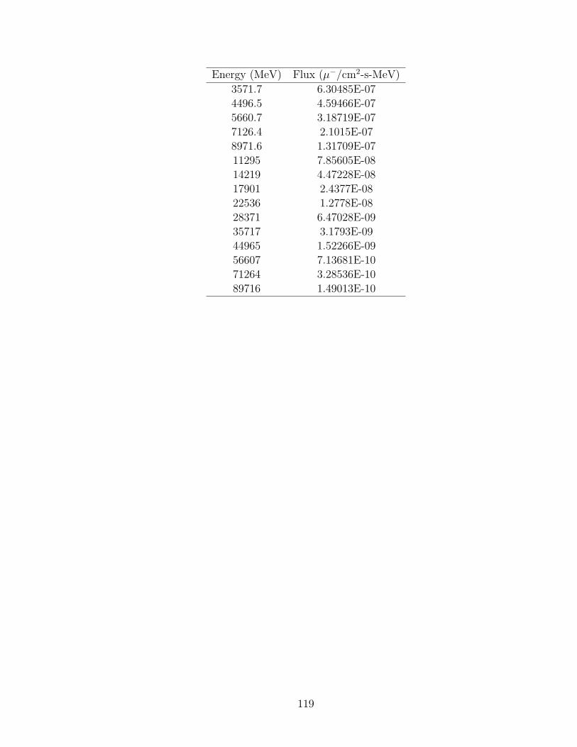
Energy (MeV) Flux (µ−/cm2-s-MeV)
3571.7 6.30485E-07
4496.5 4.59466E-07
5660.7 3.18719E-07
7126.4 2.1015E-07
8971.6 1.31709E-07
11295 7.85605E-08
14219 4.47228E-08
17901 2.4377E-08
22536 1.2778E-08
28371 6.47028E-09
35717 3.1793E-09
44965 1.52266E-09
56607 7.13681E-10
71264 3.28536E-10
89716 1.49013E-10
119
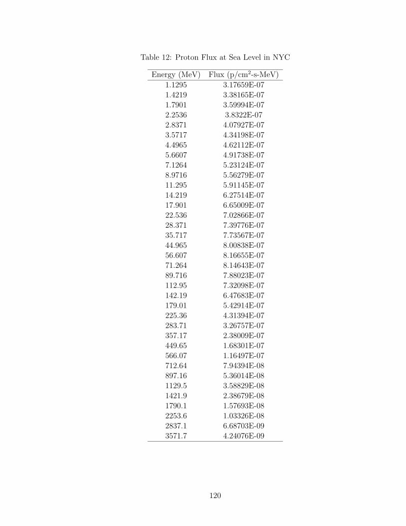
Table 12: Proton Flux at Sea Level in NYC
Energy (MeV) Flux (p/cm2-s-MeV)
1.1295 3.17659E-07
1.4219 3.38165E-07
1.7901 3.59994E-07
2.2536 3.8322E-07
2.8371 4.07927E-07
3.5717 4.34198E-07
4.4965 4.62112E-07
5.6607 4.91738E-07
7.1264 5.23124E-07
8.9716 5.56279E-07
11.295 5.91145E-07
14.219 6.27514E-07
17.901 6.65009E-07
22.536 7.02866E-07
28.371 7.39776E-07
35.717 7.73567E-07
44.965 8.00838E-07
56.607 8.16655E-07
71.264 8.14643E-07
89.716 7.88023E-07
112.95 7.32098E-07
142.19 6.47683E-07
179.01 5.42914E-07
225.36 4.31394E-07
283.71 3.26757E-07
357.17 2.38009E-07
449.65 1.68301E-07
566.07 1.16497E-07
712.64 7.94394E-08
897.16 5.36014E-08
1129.5 3.58829E-08
1421.9 2.38679E-08
1790.1 1.57693E-08
2253.6 1.03326E-08
2837.1 6.68703E-09
3571.7 4.24076E-09
120
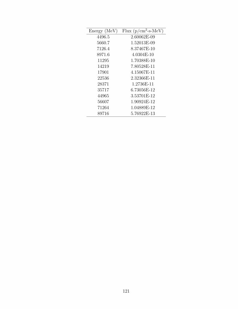
Energy (MeV) Flux (p/cm2-s-MeV)
4496.5 2.60062E-09
5660.7 1.52013E-09
7126.4 8.37467E-10
8971.6 4.0304E-10
11295 1.70388E-10
14219 7.80528E-11
17901 4.15067E-11
22536 2.32366E-11
28371 1.2736E-11
35717 6.73056E-12
44965 3.53701E-12
56607 1.90924E-12
71264 1.04889E-12
89716 5.76922E-13
121

Table 13: Neutron Flux at Sea Level in NYC
Energy (MeV) Flux (n/cm2-s-MeV)
1.1295E-08 20938.62298
1.4219E-08 23445.19265
1.7901E-08 25480.44436
2.2536E-08 26671.2223
2.8371E-08 26630.28457
3.5717E-08 25060.14341
4.4965E-08 21898.00723
5.6607E-08 17448.83997
7.1264E-08 12410.42972
8.9716E-08 7701.074385
1.1295E-07 4099.814784
1.4219E-07 1903.955814
1.7901E-07 866.1702727
2.2536E-07 485.891103
2.8371E-07 357.4277736
3.5717E-07 293.2748751
4.4965E-07 243.4056802
5.6607E-07 200.6531615
7.1264E-07 164.3170188
8.9716E-07 133.882014
1.1295E-06 108.6661063
1.4219E-06 87.9537619
1.7901E-06 71.0321301
2.2536E-06 57.27335212
2.8371E-06 46.12192279
3.5717E-06 37.10540487
4.4965E-06 29.828713
5.6607E-06 23.96451464
7.1264E-06 19.24333198
8.9716E-06 15.44580784
0.000011295 12.39285033
0.000014219 9.941030905
0.000017901 7.971716716
0.000022536 6.391150975
0.000028371 5.122927611
0.000035717 4.105590867
122
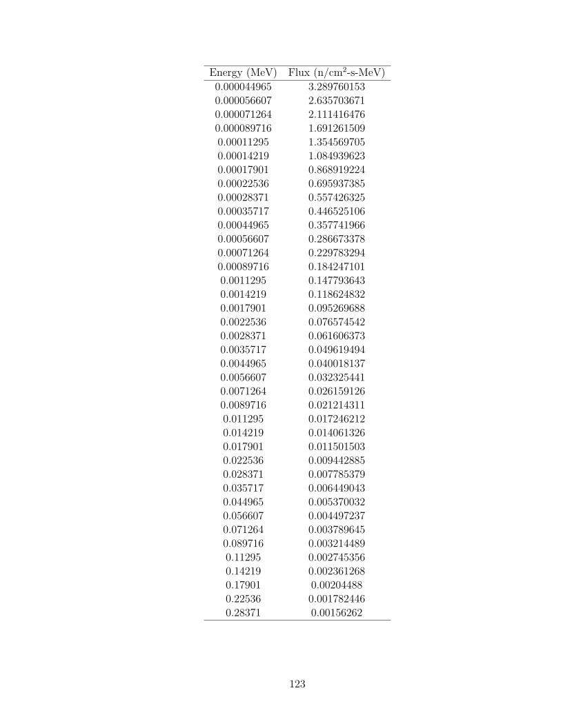
Energy (MeV) Flux (n/cm2-s-MeV)
0.000044965 3.289760153
0.000056607 2.635703671
0.000071264 2.111416476
0.000089716 1.691261509
0.00011295 1.354569705
0.00014219 1.084939623
0.00017901 0.868919224
0.00022536 0.695937385
0.00028371 0.557426325
0.00035717 0.446525106
0.00044965 0.357741966
0.00056607 0.286673378
0.00071264 0.229783294
0.00089716 0.184247101
0.0011295 0.147793643
0.0014219 0.118624832
0.0017901 0.095269688
0.0022536 0.076574542
0.0028371 0.061606373
0.0035717 0.049619494
0.0044965 0.040018137
0.0056607 0.032325441
0.0071264 0.026159126
0.0089716 0.021214311
0.011295 0.017246212
0.014219 0.014061326
0.017901 0.011501503
0.022536 0.009442885
0.028371 0.007785379
0.035717 0.006449043
0.044965 0.005370032
0.056607 0.004497237
0.071264 0.003789645
0.089716 0.003214489
0.11295 0.002745356
0.14219 0.002361268
0.17901 0.00204488
0.22536 0.001782446
0.28371 0.00156262
123
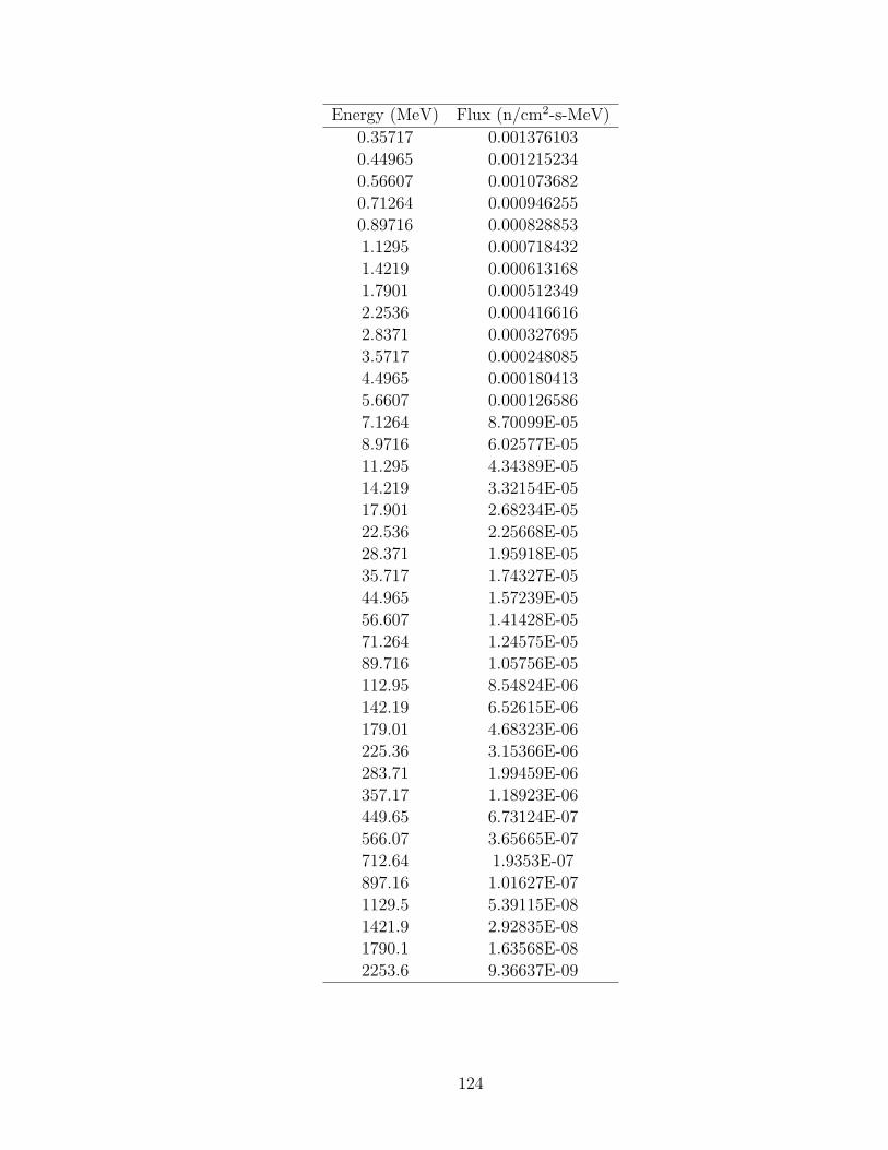
Energy (MeV) Flux (n/cm2-s-MeV)
0.35717 0.001376103
0.44965 0.001215234
0.56607 0.001073682
0.71264 0.000946255
0.89716 0.000828853
1.1295 0.000718432
1.4219 0.000613168
1.7901 0.000512349
2.2536 0.000416616
2.8371 0.000327695
3.5717 0.000248085
4.4965 0.000180413
5.6607 0.000126586
7.1264 8.70099E-05
8.9716 6.02577E-05
11.295 4.34389E-05
14.219 3.32154E-05
17.901 2.68234E-05
22.536 2.25668E-05
28.371 1.95918E-05
35.717 1.74327E-05
44.965 1.57239E-05
56.607 1.41428E-05
71.264 1.24575E-05
89.716 1.05756E-05
112.95 8.54824E-06
142.19 6.52615E-06
179.01 4.68323E-06
225.36 3.15366E-06
283.71 1.99459E-06
357.17 1.18923E-06
449.65 6.73124E-07
566.07 3.65665E-07
712.64 1.9353E-07
897.16 1.01627E-07
1129.5 5.39115E-08
1421.9 2.92835E-08
1790.1 1.63568E-08
2253.6 9.36637E-09
124
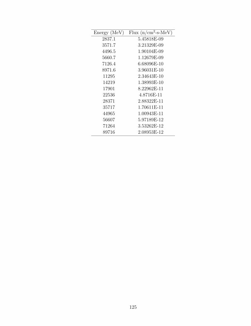
Energy (MeV) Flux (n/cm2-s-MeV)
2837.1 5.45818E-09
3571.7 3.21329E-09
4496.5 1.90104E-09
5660.7 1.12679E-09
7126.4 6.68096E-10
8971.6 3.96031E-10
11295 2.34643E-10
14219 1.38993E-10
17901 8.22962E-11
22536 4.8716E-11
28371 2.88322E-11
35717 1.70611E-11
44965 1.00943E-11
56607 5.97189E-12
71264 3.53262E-12
89716 2.08953E-12
125
REFERENCES
[1] W. L. Bendel and E. L. Petersen, “Proton upsets in orbit,” IEEE Trans. Nucl.Sci., vol. 30, no. 6, pp. 4481–4485, Dec. 1983.
[2] K. A. LaBel, M. M. Gates, A. K. Moran, P. W. Marshall, J. Barth, E. G.Stassinopoulos, C. M. Seidleck, and C. J. Dale, “Commercial microelectronicstechnologies for applications in the satellite radiation environment,” in Proc.IEEE Aerospace Applications Conf., vol. 1, Feb. 1996, pp. 375–390.
[3] K. A. LaBel, R. L. Ladbury, L. M. Cohn, and T. R. Oldham, “Radiation testchallenges for scaled commercial memories,” IEEE Trans. Nucl. Sci., vol. 55,no. 4, pp. 2174–2180, Aug. 2008.
[4] EIA/JEDEC, JESD57: Test Procedures for the Measurement of Single-EventEffects in Semiconductor Devices from Heavy Ion Irradiation. 2500 WilsonBlvd., Arlington, VA 22201: Electronic Industries Association, 1996.
[5] JEDEC, JESD89A: Measurement and Reporting of Alpha Particle and Terres-trial Cosmic Ray-Induced Soft Errors in Semiconductor Devices. 2500 WilsonBlvd., Arlington, VA 22201: JEDEC Solid State Technology Association, 2006.
[6] Semiconductor Industry Association (SIA), “International roadmap forsemiconductors 2009 edition,” 2009. [Online]. Available: http://www.itrs.net
[7] J. T. Wallmark and S. M. Marcus, “Minimum size and maximum packing den-sity of nonredundant semiconductor devices,” in Proc. of the IRE, Mar. 1962,pp. 286–298.
[8] C. Svensson, “Forty years of feature-size predictions (1962-2002),” in Dig. IEEEInt. Solid-State Circuits Conf., 2003, pp. 35–36.
[9] D. Binder, E. C. Smith, and A. B. Holman, “Satellite anomalies from galacticcosmic rays,” IEEE Trans. Nucl. Sci., vol. 22, no. 6, pp. 2675–2680, Dec. 1975.
[10] T. C. May and M. H. Woods, “Alpha-particle-induced soft errors in dynamicmemories,” IEEE Trans. Electron Devices, vol. 26, no. 1, pp. 2–9, 1979.
[11] J. F. Ziegler and W. A. Lanford, “Effect of cosmic rays on computer memories,”Sci., vol. 206, no. 4420, pp. 776–788, 1979.
[12] J. F. Ziegler, “The effect of concrete shielding on cosmic ray induced soft fails inelectronic systems,” IEEE Trans. Electron Devices, vol. 28, no. 5, pp. 560–565,May 1981.
[13] R. Silberberg, C. H. Tsao, and J. R. Letaw, “Neutron generated single-eventupsets in the atmosphere,” IEEE Trans. Nucl. Sci., vol. 31, pp. 1183–1185, Dec.1984.
126

[14] J. F. Dicello, C. W. McCabe, J. D. Doss, and M. Paciotti, “The relative effi-ciency of soft-error induction in 4K static RAMs by muons and pions,” IEEETrans. Nucl. Sci., vol. 30, no. 6, pp. 4613–4615, Dec. 1983.
[15] J. F. Dicello, M. E. Schillaci, C. W. McCabe, J. D. Doss, M. Paciotti, andP. Berardo, “Meson interactions in NMOS and CMOS static RAMs,” IEEETrans. Nucl. Sci., vol. 32, no. 6, pp. 4201–4205, Dec. 1985.
[16] J. F. Dicello, “Microelectronics and microdosimetry,” Nucl. Instrum. MethodsPhysics Res. B, vol. 24-25, no. Part 2, pp. 1044–1049, 1987.
[17] J. F. Dicello, M. Paciotti, and M. E. Schillaci, “An estimate of error rates inintegrated circuits at aircraft altitudes and at sea level,” Nucl. Instrum. MethodsPhysics Res. B, vol. 40, pp. 1295–1299, Apr. 1989.
[18] G. R. Srinivasan, H. H. K. Tang, and P. C. Murley, “Parameter-free, predictivemodeling of single event upsets due to protons, neutrons, and pions in terrestrialcosmic rays,” IEEE Trans. Nucl. Sci., vol. 41, no. 6, pp. 2063–2070, Dec. 1994.
[19] C. J. Gelderloos, R. J. Peterson, M. E. Nelson, and J. F. Ziegler, “Pion-inducedsoft upsets in 16 Mbit DRAM chips,” IEEE Trans. Nucl. Sci., vol. 44, no. 6,pp. 2237–2242, Dec. 1997.
[20] R. J. Peterson, “Radiation-induced errors in memory chips,” Brazilian J.Physics, vol. 33, no. 2, pp. 246–249, Jun. 2003.
[21] S. Duzellier, D. Falguere, M. Tverskoy, E. Ivanov, R. Dufayel, and M.-C. Calvet,“SEU induced by pions in memories from different generations,” IEEE Trans.Nucl. Sci., vol. 48, no. 6, pp. 1960–1965, Dec. 2001.
[22] H. H. K. Tang, “Nuclear physics of cosmic ray interaction with semiconductormaterials: Particle-induced soft errors from a physicist’s perspective,” IBM J.Res. and Development, vol. 40, no. 1, pp. 91–108, Jan. 1996.
[23] E. Normand, “Single event upset at ground level,” IEEE Trans. Nucl. Sci.,vol. 43, no. 6, pp. 2742–2750, Dec. 1996.
[24] J. F. Ziegler and H. Puchner, SER–History, Trends, and Challenges: A Guidefor Designing with Memory ICs. Cypress Semiconductor Corporation, 2004.
[25] S. Duzellier, R. Ecoffet, D. Falguere, T. Nuns, L. Guibert, W. Hajdas, andM. C. Calvert, “Low energy proton induced SEE in memories,” IEEE Trans.Nucl. Sci., vol. 44, no. 6, pp. 2306–2310, Dec. 1997.
[26] E. L. Petersen, P. Shapiro, J. H. Adams Jr., and E. A. Burke, “Calculationof cosmic-ray induced soft upsets and scaling in VLSI devices,” IEEE Trans.Nucl. Sci., vol. 29, no. 6, pp. 2055–2063, Dec. 1982.
127
[27] E. Petersen, “Single event analysis and prediction,” in Proc. IEEE NSRECShort Course, 1997.
[28] R. H. Dennard, F. H. Gaensslen, H.-N. Yu, V. L. Rideout, E. Bassous, andA. R. LeBlanc, “Design of ion-implanted MOSFET’s with very small physicaldimensions,” IEEE J. Solid-State Circuits, vol. SC-9, no. 5, pp. 256–268, Oct.1974.
[29] R. Baumann, “The impact of technology scaling on soft error rate performanceand limits to the efficacy of error correction,” in Dig. IEEE Int. Electron DevicesMeeting, 2002, pp. 329–332.
[30] S. Gerardin, M. Bagatin, P. Rech, A. Cester, and A. Paccagnella, “Exploitinga low-energy accelerator to test commercial electronics with low-LET protonbeams,” in presented at the Radiation Effects Components and Systems Work-shop, Athens, Greece, 2006.
[31] D. F. Heidel, K. P. Rodbell, P. Oldiges, M. S. Gordon, H. H. K. Tang, E. H.Cannon, and C. Plettner, “Single-event-upset critical charge measurements andmodeling of 65 nm silicon-on-insulator latches and memory cells,” IEEE Trans.Nucl. Sci., vol. 53, no. 6, pp. 3512–3517, Dec. 2006.
[32] K. P. Rodbell, D. F. Heidel, H. H. K. Tang, M. S. Gordon, P. Oldiges, andC. E. Murray, “Low-energy proton-induced single-event-upsets in 65 nm node,silicon-on-insulator, latches and memory cells,” IEEE Trans. Nucl. Sci., vol. 54,no. 6, pp. 2474–2479, Dec. 2007.
[33] D. F. Heidel, P. W. Marshall, K. A. LaBel, J. R. Schwank, K. P. Rodbell, M. C.Hakey, M. D. Berg, P. E. Dodd, M. R. Friendlich, A. D. Phan, C. M. Seidleck,M. R. Shaneyfelt, and M. A. Xapsos, “Low energy proton single-event-upsettest results on 65 nm SOI SRAM,” IEEE Trans. Nucl. Sci., vol. 55, no. 6, pp.3394–3400, Dec. 2008.
[34] H. Kobayashi, N. Kawamoto, J. Kase, and K. Shiraish, “Alpha particle andneutron-induced soft error rates and scaling trends in SRAM,” in Proc. IEEEInt. Physics Rel. Symp., Apr. 2009, pp. 206–211.
[35] H. Bichsel, D. E. Groom, and S. R. Klein, “Passage of particles through matter,”Physics Lett. B, vol. 667, no. 1-5, pp. 267–280, 2008.
[36] Stopping Powers and Ranges for Protons and Alpha Particles. Bethesda, MD:International Commission on Radiation Units and Measurements, 1993, vol.ICRU report 49.
[37] J. F. Ziegler, “Stopping of energetic light ions in elemental matter,” J. AppliedPhysics, vol. 85, no. 3, pp. 1249–1272, 1999.
128
[38] P. Wojciechowski, P. Baumann, H. Daniel, F. J. Hartmann, C. Herrmann,M. Mhlbauer, W. Schott, A. Fuchs, P. Hauser, K. Lou, C. Petitjean, D. Taqqu,and F. Kottmann, “Measurement of the stopping power for µ− and µ+ at en-ergies between 3 keV and 100 keV,” Hyperfine Interactions, vol. 82, no. 1, pp.127–131, 1993.
[39] F. J. Hartmann, H. Daniel, C. Maierl, M. Mhlbauer, W. Schott, P. Wo-jciechowski, P. Hauser, C. Petitjean, D. Taqqu, F. Kottmann, and V. E.Markushin, “Experiments with low-energy muons,” Hyperfine Interactions, vol.101-102, no. 1, pp. 623–632, 1996.
[40] D. E. Groom, N. V. Mokhov, and S. I. Striganov, “Muon stopping power andrange tables 10 MeV-100 TeV,” Atomic Data and Nucl. Data Tables, vol. 78,pp. 183–356, Jul. 2001.
[41] F. Wrobel, “Use of nuclear codes for neutron-induced nuclear reactions in mi-croelectronics,” in IEEE Int. On-Line Testing Symp., Jul. 2005, pp. 82–86.
[42] R. A. Reed, R. A. Weller, R. D. Schrimpf, M. H. Mendenhall, K. M. Warren, andL. W. Massengill, “Implications of nuclear reactions for single event effects testmethods and analysis,” IEEE Trans. Nucl. Sci., vol. 53, no. 6, pp. 3356–3362,Dec. 2006.
[43] A. Wyttenbach, P. Baertschi, S. Bajo, J. Hadermann, K. Junker, S. Katcoff,E. A. Hermes, and H. S. Pruys, “Probabilities of muon induced nuclear reactionsinvolving charged particle emission,” J. Nucl. Physics A, vol. 294, pp. 278–292,Jan. 1978.
[44] B. Rossi, “Interpretation of cosmic-ray phenomena,” Reviews Modern Physics,vol. 20, no. 3, pp. 537–583, Jul. 1948.
[45] P. K. Grieder, Cosmic Rays at Earth. Amsterdam: Elsevier, 2001.
[46] ISO, ISO 15390:2004: Space Environment (Natural and Artifical) - Galacticcosmic Ray Model. Geneva, Switzerland: International Organization for Stan-dardization, 2004.
[47] G. D. Badhwar and P. M. O’Neill, “Galactic cosmic radiation model and itsapplications,” Advances in Space Research, vol. 17, no. 2, pp. 7–17, 1996.
[48] A. J. Tylka, J. H. Adams Jr., P. R. Boberg, B. Brownstein, W. F. Dietrich,E. O. Flueckiger, E. L. Petersen, M. A. Shea, D. F. Smart, and E. C. Smith,“CREME96: A revision of the cosmic ray effects on micro-electronics code,”IEEE Trans. Nucl. Sci., vol. 44, no. 6, pp. 2150–2160, Dec. 1997.
[49] R. A. Nymmik, M. I. Panasyuk, T. I. Pervaja, and A. A. Suslov, “A model ofgalactic cosmic ray fluxes,” Int. J. Radiation Applications and Instrumentation.Part D. Nucl. Tracks and Radiation Measurements, vol. 20, no. 3, pp. 427–429,1992.
129
[50] J. A. V. Allen, C. E. McIlwain, and G. H. Ludwig, “Radiation observationswith satellite 1958 ε,” J. Geophysical Res., vol. 64, no. 3, pp. 271–286, 1959.
[51] D. M. Sawyer and J. I. Vette, “AP-8 trapped proton environment for solarmaximum and solar minimum,” NASA National Space Science Data Center,Tech. Rep., Dec. 1976.
[52] J. L. Barth, C. S. Dyer, and E. G. Stassinopoulos, “Space, atmospheric, andterrestrial radiation environments,” IEEE Trans. Nucl. Sci., vol. 50, no. 3, pp.466–482, Jun. 2003.
[53] E. G. Stassinopoulos and J. P. Raymond, “The space radiation environment forelectronics,” Proc. of the IEEE, vol. 76, no. 11, pp. 1423–1442, Nov. 1988.
[54] E. G. Mullen, M. S. Gussenhoven, K. Ray, and M. Violet, “A double-peakedinner radiation belt: cause and effect as seen on CRRES,” IEEE Trans. Nucl.Sci., vol. 38, no. 6, pp. 1713–1718, Dec. 1991.
[55] D. P. Bhattacharyya, M. Mukherjee, and D. Basu, “The spectra of cosmicpions and nucleons at low and high geomagnetic latitudes at the top of theatmosphere,” Annalen der Physik, vol. 487, no. 3, pp. 161–165, 1975.
[56] P. Papini, C. Grimani, and S. A. Stephens, “An estimate of the secondary-proton spectrum at small atmospheric depths,” Nuovo Cimento C GeophysicsSpace Physics C, vol. 19, pp. 367–387, Jun. 1996.
[57] T. Sanuki, “BESS data on primary cosmic rays and muons,” Nucl. Physics B -Proceedings Supplements, vol. 100, no. 1-3, pp. 121–123, 2001.
[58] M. Boezio, V. Bonvicini, P. Schiavon, A. Vacchi, N. Zampa, D. Bergstrm,P. Carlson, T. Francke, P. Hansen, E. Mocchiutti, M. Suffert, M. Hof, J. Kre-mer, W. Menn, M. Simon, M. Ambriola, R. Bellotti, F. Cafagna, F. Ciacio,M. Circella, C. N. D. Marzo, N. Finetti, P. Papini, S. Piccardi, P. Spillan-tini, E. Vannuccini, S. Bartalucci, M. Ricci, M. Casolino, M. P. D. Pascale,A. Morselli, P. Picozza, R. Sparvoli, J. W. Mitchell, J. F. Ormes, S. A. Stephens,R. E. Streitmatter, U. Bravar, and S. J. Stochaj, “The cosmic-ray proton andhelium spectra measured with the caprice98 balloon experiment,” AstroparticlePhysics, vol. 19, no. 5, pp. 583–604, 2003.
[59] K. O’Brien, W. Friedberg, H. H. Sauer, and D. F. Smart, “Atmospheric cos-mic rays and solar energetic particles at aircraft altitudes,” Environment Int.,vol. 22, no. Supplement 1, pp. 9–44, 1996, the Natural Radiation EnvironmentVI.
[60] C. Hagmann, D. Lange, and D. Wright, “Monte Carlo simulation of proton-induced cosmic-ray cascades in the atmosphere,” Lawrence Livermore NationalLaboratory, Livermore, CA, Tech. Rep. UCRL-TM-229452, Feb. 2007.
130
[61] L. Desorgher, E. O. Fluckiger, M. Gurtner, M. R. Moser, and R. Butikofer,“Atmocosmics: A Geant4 code for computing the interaction of cosmic rayswith the earth’s atmosphere,” Int. J. Modern Physics, vol. 20, pp. 6802–6804,2005.
[62] M. Tueros and S. Sciutto, “TIERRAS: A package to simulate high energy cos-mic ray showers underground, underwater and under-ice,” Computer PhysicsCommunications, vol. 181, no. 2, pp. 380–392, 2010.
[63] G. Carminati, M. Bazzotti, A. Margiotta, and M. Spurio, “Atmospheric muonsfrom parametric formulas: a fast generator for neutrino telescopes (MUPAGE),”Computer Physics Communications, vol. 179, no. 12, pp. 915–923, 2008.
[64] F. Lei, S. Clucas, C. Dyer, and P. Truscott, “An atmospheric radiation modelbased on response matrices generated by detailed Monte Carlo simulations ofcosmic ray interactions,” IEEE Trans. Nucl. Sci., vol. 51, no. 6, pp. 3442–3451,Dec. 2004.
[65] F. Lei, A. Hands, S. Clucas, C. Dyer, and P. Truscott, “Improvements to andvalidations of the QinetiQ atmospheric radiation model (QARM),” in Proc.IEEE Radiation Effects Components and Systems, Sep. 2005, pp. D3–1–D3–8.
[66] “EXPACS homepage.” [Online]. Available: http://phits.jaea.go.jp/expacs/
[67] T. Sato, H. Yasuda, K. Niita, A. Endo, and L. Sihver, “Development of PARMA:PHITS-based analytical radiation model in the atmosphere,” Radiation Res.,vol. 170, no. 2, pp. 244–259, 2008.
[68] M. S. Gordon, P. Goldhagen, K. P. R. T. H. Zabel, H. H. K. Tang, J. M. Clem,and P. Bailey, “Measurement of the flux and energy spectrum of cosmic-rayinduced neutrons on the ground,” IEEE Trans. Nucl. Sci., vol. 51, no. 6, pp.3427–3434, Dec. 2004.
[69] C.-R. R. Section, “Nagoya multi-directional muon telescope,” Solar-TerrestrialEnvironment Laboratory, Tech. Rep., 2002.
[70] G. Brooke and A. W. Wolfendale, “The momentum spectrum of cosmic rayprotons near sea level in the momentum range 0.6-150 gev/c,” Proc. PhysicalSoc., vol. 83, 1964.
[71] A. Z. Rosen, “Proton intensities at sea level and 9000 feet,” Physical Review,vol. 93, no. 1, pp. 211–214, Jan. 1954.
[72] A. W. Wolfendale and G. D. Rochester, Cosmic rays at ground level. Edited byA. W. Wolfendale. Institute of Physics London, 1973.
[73] C. E. Miller, J. E. Henderson, D. S. Potter, J. Todd, W. M. Sandstrom, G. R.Garrison, W. R. Davis, and F. M. Charbonnier, “The zenith angle dependenceof cosmic-ray protons,” Physical Review, vol. 93, no. 3, pp. 590–595, Feb 1954.
131
[74] G. N. Roesler Jr., “The zenith-angle distribution of stopping muons at sea level,and the response of a stopping-muon cosmic-ray detector,” Naval Academy,Annapolis, MD, Tech. Rep., May 1975.
[75] O. C. Allkofer, K. Carstensen, and W. D. Dau, “The absolute cosmic ray muonspectrum at sea level,” Physics Lett. B, vol. 36, no. 4, pp. 425–427, 1971.
[76] M. Boezio, V. Bonvicini, P. Schiavon, A. Vacchi, N. Zampa, D. Bergstrom,P. Carlson, T. Francke, P. Hansen, E. Mocchiutti, M. Suffert, M. Hof, J. Kre-mer, W. Menn, M. Simon, M. Ambriola, R. Bellotti, F. Cafagna, F. Ciacio,M. Circella, C. N. De Marzo, P. Papini, S. Piccardi, P. Spillantini, E. Vannuc-cini, S. Bartalucci, and M. Ricci, “Energy spectra of atmospheric muons mea-sured with the CAPRICE98 balloon experiment,” Physical Review D, vol. 67,no. 7, p. 072003, Apr. 2003.
[77] E. P. George and J. Evans, “Further observations of cosmic-ray events in nuclearemulsions exposed below ground,” Proc. Physical Soc. A, vol. 68, no. 9, p. 829,1955.
[78] H. E. Hall, Jr. and M. E. Richmond, “Stopping rate and energy loss of cosmicray muons in sand,” J. Geophysical Res., vol. 79, pp. 5503–5506, Dec. 1974.
[79] G. Spannagel and E. L. Fireman, “Stopping rate of negative cosmic-ray muonsnear sea level,” J. Geophysical Res., vol. 77, no. 28, pp. 5351–5359, 1972.
[80] S.-I. Kaneko, T. Kubozoe, M. Okazaki, and M. Takahata, “Observations of slowparticles and stars in nuclear emulsions exposed at 17 m.w.e. underground,” J.Physical Soc. Japan, vol. 10, pp. 600–+, Aug. 1955.
[81] A. M. Short, “Mesons stopped underground,” Proc. Physical Soc., vol. 81, no. 5,p. 841, 1963.
[82] C. C. Foster, S. L. Casey, A. L. Johnson, P. Miesle, N. Sifri, A. H. Skees,and K. M. Murray, “Radiation effects test facility at the Indiana UniversityCyclotron Facility,” in Int. Conf. Application Accelerators in Res. and Industry,J. Duggan and I. L. Morgan, Eds., vol. 392, no. 1. AIP, 1997, pp. 1131–1134.
[83] C. M. Castaneda, “Crocker Nuclear Laboratory (CNL) radiation effects mea-surement and test facility,” in IEEE Radiation Effects Data Workshop, 2001,pp. 77–81.
[84] G. M. Marshall, “Muon beams and facilities at TRIUMF,” Zeitschrift fur PhysikC Particles and Fields, vol. 56, pp. 226–+, Mar. 1992.
[85] J. H. Brewer, “µ+sr with surface muon beams,” Hyperfine Interactions, vol. 8,no. 4, pp. 831–834, Jan. 1981.
[86] J. Doornbos, private communication, 1983.
132

[87] H. Paul, “Stopping power for light ions.” [Online]. Available: http://www.exphys.uni-linz.ac.at/Stopping/
[88] H. Paul and A. Schinner, “An empirical approach to the stopping power ofsolids and gases for ions from 3Li to 18Ar – part II,” Nucl. Instrum. MethodsPhysics Res. B, vol. 195, pp. 166–174, 2002.
[89] J. F. Zeigler, M. D. Zeigler, and J. P. Biersack, “Stopping and range of ions inmatter SRIM.” [Online]. Available: http://www.srim.org/
[90] J. J. Suter, J. M. C. J. R. Norton, D. Y. Kusnierkiewicz, and A. M. Koehler,“Simulation of low-earth-orbit radiation environments with a 5 to 120 MeVproton cyclotron beam using a proton beam modulator,” IEEE Trans. Nucl.Sci., vol. 34, no. 4, pp. 1070–1075, Aug. 1987.
[91] E. W. Cascio and S. Sarkar, “A solar flare simulation wheel for the radiationtest beamline at the Francis H. Burr Proton Therapy Center,” IEEE Trans.Nucl. Sci., vol. 55, no. 6, pp. 3428–3434, Dec. 2008.
[92] J. R. Letaw, R. Silberberg, and C. H. Tsao, “Proton-nucleus total inelastic crosssections - an empirical formula for E greater than 10 MeV,” Astrophysical J.Supplement Series, vol. 51, pp. 271–275, Mar. 1983.
[93] W. J. Stapor, J. P. Meyers, J. B. Langworthy, and E. L. Petersen, “Two pa-rameter bendel model calculations for predicting proton induced upset,” IEEETrans. Nucl. Sci., vol. 37, no. 6, pp. 1966–1973, Dec. 1990.
[94] Y. Cao, T. Sato, M. Orshansky, D. Sylvester, and C. Hu, “New paradigm ofpredictive mosfet and interconnect modeling for early circuit simulation,” inProc. IEEE Custom Integrated Circuits Conf., 2000, pp. 201–204.
[95] W. Zhao and Y. Cao, “New generation of predictive technology model for sub-45 nm early design exploration,” IEEE Trans. Electron Devices, vol. 53, no. 11,pp. 2816–2823, Nov. 2006.
[96] “Predictive technology model (ptm),” [Online] Available: http://ptm.asu.edu.
[97] Semiconductor Industry Association (SIA), “International roadmap forsemiconductors 2010 update,” 2010. [Online]. Available: http://www.itrs.net
[98] J. S. Kauppila, A. L. Sternberg, M. L. Alles, A. M. Francis, J. Holmes, O. A.Amusan, and L. W. Massengill, “A bias-dependent single-event compact modelimplemented into BSIM4 and a 90 nm CMOS process design kit,” IEEE Trans.Nucl. Sci., vol. 56, pp. 3152–3157, Dec. 2009.
[99] R. Naseer, Y. Boulghassoul, J. Draper, S. DasGupta, and A. Witulski, “Criticalcharge characterization for soft error rate modeling in 90 nm SRAM,” in IEEESymp. Circuits and Systems, May 2007, pp. 1879–1882.
133

[100] T. D. Loveless, M. L. Alles, D. R. Ball, K. M. Warren, and L. W. Massengill,“Parametric variability affecting 45 nm SOI SRAM single event upset cross-sections,” IEEE Trans. Nucl. Sci., vol. 57, no. 6, pp. 3228–3233, Dec. 2010.
[101] R. A. Weller, M. H. Mendenhall, R. A. Reed, R. D. Schrimpf, K. M. Warren,B. D. Sierawski, and L. W. Massengill, “Monte Carlo simulation of single eventeffects,” IEEE Trans. Nucl. Sci., vol. 57, no. 4, pp. 1726–1746, Aug. 2010.
[102] S. Agostinelli et al., “G4–a simulation toolkit,” Nucl. Instrum. Methods PhysicsRes. A, vol. 506, no. 3, pp. 250–303, 2003.
[103] M. H. Mendenhall and R. A. Weller, “An algorithm for computing screenedcoulomb scattering in Geant4,” Nucl. Instrum. Methods Physics Res. B, vol.227, no. 3, pp. 420–430, 2005.
[104] A. S. Kobayashi, D. R. Ball, K. M. Warren, R. A. Reed, N. Haddad, M. H.Mendenhall, R. D. Schrimpf, and R. A. Weller, “The effect of metallizationlayers on single event susceptibility,” IEEE Trans. Nucl. Sci., vol. 52, no. 6, pp.2189–2193, Dec. 2005.
[105] K. M. Warren, B. D. Sierawski, R. A. Weller, R. A. Reed, M. H. Mendenhall,J. A. Pellish, R. D. Schrimpf, L. W. Massengill, M. E. Porter, and J. D. Wilkin-son, “Predicting thermal neutron-induced soft errors in static memories usingTCAD and physics-based Monte Carlo simulation tools,” IEEE Electron DeviceLett., vol. 28, no. 2, pp. 180–182, Feb. 2007.
[106] Y.-K. Choi, K. Asano, N. Lindert, V. Subramanian, T.-J. King, J. Bokor, andC. Hu, “Ultrathin-body SOI MOSFET for deep-sub-tenth micron era,” IEEEElectron Device Lett., vol. 21, no. 5, pp. 254–255, May 2000.
[107] P. Oldiges, R. Dennard, D. Heidel, T. Ning, K. Rodbell, H. Tang, M. Gordon,and L. Wissel, “Technologies to further reduce soft error susceptibility in SOI,”in IEEE Int. Electron Devices Meeting, Dec. 2009, pp. 1–4.
[108] W. Xusheng, Z. Shengdong, M. Chan, and P. Chan, “Design of sub-50 nmultrathin-body (UTB) SOI MOSFETs with raised S/D,” in IEEE Conf. Elec-tron Devices and Solid-State Circuits, Dec. 2003, pp. 251–254.
[109] H. Kawasaki, V. S. Basker, T. Yamashita, C.-H. Lin, Y. Zhu, J. Faltermeier,S. Schmitz, J. Cummings, S. Kanakasabapathy, H. Adhikari, H. Jagannathan,A. Kumar, K. Maitra, J. Wang, C.-C. Yeh, C. Wang, M. Khater, M. Guil-lorn, N. Fuller, J. Chang, L. Chang, R. Muralidhar, A. Yagishita, R. Miller,Q. Ouyang, Y. Zhang, V. K. Paruchuri, H. Bu, B. Doris, M. Takayanagi,W. Haensch, D. McHerron, J. O’Neill, and K. Ishimaru, “Challenges and solu-tions of FinFET integration in an SRAM cell and a logic circuit for 22 nm nodeand beyond,” in IEEE Int. Electron Devices Meeting, Dec. 2009, pp. 1–4.
134


