
B. Raja et al. Int. Journal of Engineering Research and Applications www.ijera.com
ISSN: 2248-9622, Vol. 5, Issue 11, (Part - 1) November 2015, pp.57-68
www.ijera.com 57 | P a g e
Thermal Simulations of an Electronic System using Ansys Icepak
B. Raja1, V. Praveenkumar
2, M. Leelaprasad
3, P. Manigandan
4
1Asst.Professor, Department of Electronics and Communication, Dr. MGR Educational and Research Institute
University, Maduravoyal, Chennai. 2,3,4
BTech Student, Department of Electronics and Communication, Dr. MGR Educational and Research
Institute University, Maduravoyal, Chennai.
ABSTRACT Present electronics industry component sizes are efficiently reducing to meet the product requirement with
compact size with greater performance in compact size products resulting in different problems from thermal
prospective to bring product better performance electrically and mechanically.
In this paper we will study how to overcome the thermal problem for a product which includes components
reliability and PCB performance by using CFD thermal simulation tool (Ansys Icepak).
I. INTRODUCTION Designing a cost competitive power electronics
system requires careful consideration of the thermal
domain as well as the electrical domain. Over
designing the system adds unnecessary cost and
weight; under designing the system may lead to
overheating and even system failure. Finding an
optimized solution requires a good understanding of
how to predict the operating temperatures of the
system’s power components and how the heat
generated by those components affects neighboring
devices, such as capacitors and microcontrollers.
No single thermal analysis tool or technique
works best in all situations. Good thermal
assessments require a combination of analytical
calculations using thermal specifications, empirical
analysis and thermal modeling. The art of thermal
analysis involves using all available tools to support
each other and validate their conclusions. Power
devices and low lead count packages are the primary
focus, but the concepts herein are general and can be
applied to lower power components and higher lead
count devices such as microcontrollers.
II. HEAT TRANSFER THEORY Three basic natural laws of physics:
a. Heat will always be transferred from a hot
medium to a cold medium, until equilibrium is
reached.
b. There must be a temperature difference
c. The heat lost by the hot medium is equal to the
amount of heat gained by the cold medium,
except for losses to the surroundings.
Modes of Heat Transfer Conduction
Convection
Radiation
Conduction
Fig:1 Conduction
TABLE 1
Thermal Conductivity of various materials
Material W/mK
Aluminum (Pure) 216
Aluminum Nitride 230
Alumina 25
Copper 398
Diamond 2300
Epoxy (No fill) 0.2
Epoxy (High fill) 2.1
Epoxy glass 0.3
Gold 296
Lead 32.5
Silicon 144
Silicon Carbide 270
Silicon Grease 0.2
Solder 49.3
Convection One of the mechanism of heat transfer occurring
because of bulk motion (observable movement) of
fluids. Heat is the entity of interest being adverted
(carried), and diffused (dispersed). This can be
contrasted with conductive heat transfer, which is the
transfer of energy by vibrations at a molecular level
RESEARCH ARTICLE OPEN ACCESS

B. Raja et al. Int. Journal of Engineering Research and Applications www.ijera.com
ISSN: 2248-9622, Vol. 5, Issue 11, (Part - 1) November 2015, pp.57-68
www.ijera.com 58 | P a g e
through a solid or fluid, and radioactive, the transfer
of energy through electromagnetic waves.
Convection mode There are two major mode of convection,
Natural Convection or free convection
Forced Convection
Natural convection Natural convection, or free convection, occurs
due to temperature differences which affect the
density, and thus relative buoyancy, of the fluid.
Heavier (more dense) components will fall, while
lighter (less dense) components rise, leading to
bulk fluid movement. Natural convection can only
occur, therefore, in a gravitational field. A common
example of natural convection is the rise of smoke
from a fire. it can be seen in a pot of boiling water in
which the hot and less-dense water on the bottom
layer moves upwards in plumes, and the cool and
more dense water near the top of the pot likewise
sinks.
Forced convection In forced convection, also called heat advection,
fluid movement results from external surface
forces such as a fan or pump. Forced convection is
typically used to increase the rate of heat exchange.
Many types of mixing also utilize forced convection
to distribute one substance within another. Forced
convection also occurs as a by-product to other
processes, such as the action of a propeller in a fluid
or aerodynamic heating. Fluid radiator systems, and
also heating and cooling of parts of the body by
blood circulation, are other familiar examples of
forced convection.
Radiation Thermal radiation is energy emitted by matter
as electromagnetic waves due to the pool of thermal
energy that all matter possesses that has a
temperature above absolute zero. Thermal radiation
propagates without the presence of matter through
the vacuum of space.
Thermal radiation is a direct result of the random
movements of atoms and molecules in matter. Since
these atoms and molecules are composed of charged
particles (protons and electrons), their movement
results in the emission of electromagnetic radiation,
which carries energy away from the surface.
III. TYPES OF FLOW LAMINAR FLOW
TURBULANT FLOW
Laminar flow It is also called as streamline flow, which is
occurs, when a fluid flows in parallel layers with no
disruption between the layers. There are no cross
currents perpendicular to the direction of flow,
nor eddies or swirls of fluids. In laminar flow the
motion of the particles of fluid is very orderly with
all particles moving in straight lines parallel to the
pipe walls. In fluid dynamics, laminar flow is a flow
regime characterized by high momentum diffusion
and low momentum convection.
Fig: 2 Laminar Flow
Turbulence or Turbulent flow
Is a flow regime characterised by chaotic
and stochastic property changes. This includes
low momentum diffusion, high momentum
Convection and rapid variation of pressure and
velocity in space and time. Nobel Laureate Richard
Feynman described turbulence as "the most important
unsolved problem of classical physics" Flow in which
the kinetic energy dies out due to the action of fluid
molecular viscosity is called laminar flow. While
there is no theorem relating the non-
dimensional Reynolds number (Re) to turbulence
flows at Reynolds numbers larger than 100000 are
typically (but not necessarily) turbulent while those at
low Reynolds numbers usually remain laminar.
Fig: 3 Turbulent Flow
IV. PRINTED CIRCUIT BOARD A printed circuit board (PCB), is used to
mechanically support and electrically connect
electronic components using conductive pathways,
tracks or signal traces etched from copper sheets
laminated onto a non-conductive substrate. It is also
referred to as printed wiring board (PWB) or etched

B. Raja et al. Int. Journal of Engineering Research and Applications www.ijera.com
ISSN: 2248-9622, Vol. 5, Issue 11, (Part - 1) November 2015, pp.57-68
www.ijera.com 59 | P a g e
wiring board. Printed circuit boards are used in
virtually all but the simplest commercially produced
electronic devices.
Fig: 4 Printed Circuit Board
A PCB populated with electronic components is
called a printed circuit assembly (PCA), printed
circuit board assembly or PCB Assembly (PCBA). In
informal use the term "PCB" is used both for bare
and assembled boards, the context clarifying the
meaning.
Fig: 5 Cross Section of Printed Circuit Board
Material Core: Copper sheet
Prepreg: It is a non conductive material to separate
two copper sheets.
V. ELECTRONIC COMPONENTS An electronic component is a basic
indivisible electronic element that is available in a
discrete form. Electronic components are discrete
devices or discrete components, mostly industrial
products and not to be confounded with electrical
elements which are conceptual abstractions
representing idealized electronic components.
Electronic components have two or more
electrical terminals (or leads). These leads connect,
usually soldered to a printed circuit board to create
an electronic circuit (a discrete circuit) with a
particular function (for example an amplifier, radio
receiver or oscillator). Basic electronic components
may be packaged discretely as arrays or networks of
like components or integrated inside of packages
such as semiconductor integrated circuits, hybrid
integrated circuits or thick film devices.
TABLE 2
COMPONENTS HISTORY
COMPONENT TYPE IMAGE
DIP
QFP
SOIC
QFN
BGA
SON
Construction of Component
Fig: 6 Construction of component Materials
VI. AIM AND SCOPE Reducing the operating temperature and increase
the product life, An operating temperature is
the temperature at which an electrical or mechanical
device operates. The device will operate effectively
within a specified temperature range which varies
based on the device function and application context
and ranges from the minimum operating
temperature to the maximum operating
temperature (or peak operating temperature). Outside
this range of safe operating temperatures the device
may fail. Aerospace and military-grade devices
generally operate over a broader temperature range
than industrial devices commercial-grade devices
generally have the lowest operating temperature
range.
At elevated temperatures a silicon device can fail
catastrophically, but even if it doesn't its electrical
characteristics frequently undergo intermittent or
permanent changes. Manufacturers of processors and
other computer components specify a maximum
operating temperature for their products. Most
devices are not certified to function properly beyond
50°C-80°C (122°F-176°F). However, in a loaded PC
with standard cooling, operating temperatures can
easily exceed the limits. The result can be memory
errors, hard disk read-write errors, faulty video and
other problems not commonly recognized as heat
related.

B. Raja et al. Int. Journal of Engineering Research and Applications www.ijera.com
ISSN: 2248-9622, Vol. 5, Issue 11, (Part - 1) November 2015, pp.57-68
www.ijera.com 60 | P a g e
The life of an electronic device is directly related
to its operating temperature. Each 10°C (18°F)
temperature rise reduces component life by 50%.
Conversely, each 10°C (18°F) temperature reduction
increases component life by 100%. Therefore, it is
recommended that computer components be kept as
cool as possible (within an acceptable noise level) for
maximum reliability, longevity and return on
investment.
VII. DEFINITIONS The terms used for thermal analysis vary
somewhat throughout the industry. Some of the most
commonly used thermal definitions and notations are
TA-Temperature at reference point ―A‖ (°c)
TJ-Junction temperature, often assumed to be constant
across the die surface (°c)
TC - Package temperature at the interface between
the package and its heat sink should be the hottest
spot on the package surface and in the dominant
thermal path (°c)
ΔTAB- Temperature difference between reference
points ―A‖ and ―B‖ (°c)
q - Heat transfer per unit time (W)
PD -Power dissipation, source of heat flux (Watts)
H- Heat flux, rate of heat flow across a unit area
(J·m- 2·s-1) (°c)
RQAB - Thermal resistance between
reference points ―A‖ and ―B‖ or RTHAB (°c)
RQJMA - Junction to moving air ambient thermal
resistance (°c/w)
RQJC - Junction to case thermal resistance of a
packaged component from the surface of its silicon to
its thermal tab or RTHJC (°c/w)
RQJA -Junction to ambient thermal resistance or RTHJA
CQAB Thermal Capacitance between reference points
―A‖ and ―B‖ or CTHAB (°c/w)
ZQAB -Transient thermal impedance between
reference points ―A‖ and ―B‖ or ZTHAB
ΔTJA = (TJ – TA) = PD RӨJA
we can easily derive the often used equation for
estimating junction temperature:
TJ = TA + (PD RӨJA)
For example, let’s assume that:
RӨJA = 30°C/W
PD = 2.0W
TA = 75.C
Then, by substitution:
TJ = TA + (PD RӨJA)
TJ = 75°C + (2.0W * 30°C/W)
TJ = 75°C + 60°C
TJ = 135°C
A cautionary note is in order here. The thermal
conductivities of some materials vary significantly
with temperature. Silicon’s conductivity, for
example, falls by about half over the min-max
operating temperature range of semiconductor
devices. If the die’s thermal resistance is a significant
portion of the thermal stack-up, then this temperature
dependency needs to be included in the analysis.
VIII. JUNCTION TEMPERATURE The term junction temperature became
commonplace in the early days of semiconductor
thermal analysis when bipolar transistors and
rectifiers were the prominent power technologies.
Presently the term is reused for all power devices,
including gate isolated devices like power MOSFETs
and IGBTs. Using the concept ―junction temperature‖
assumes that the die’s temperature is uniform across
its top surface. This simplification ignores the fact
that x-axis and y-axis thermal gradients always exist
and can be large during high power conditions or
when a single die has multiple heat sources.
Analyzing gradients at the die level almost always
requires modeling tools or very special empirical
techniques. Most of the die’s thickness is to provide
mechanical support for the very thin layer of active
components on its surface. For most thermal analysis
purposes, the electrical components on the die reside
at the chip’s surface. Except for pulse widths in the
range of hundreds of microseconds or less, it is safe
to assume that the power is generated at the die’s
surface.
IX. THERMAL MODEL The challenge of accurately predicting junction
temperatures of IC components in system-level CFD
simulations has engaged the engineering community
for a number of years. The primary challenge has
been that near-exact physical models of such
components (known as detailed thermal models, or
DTMs) are difficult to implement directly in system
designs due to the wide disparity in length scales
involved, which results in large computational
inefficiencies. A compact thermal model (CTM)
attempts to solve this problem by taking a detailed
model and extracting an abstracted, far less grid-
intensive representation that is still able to preserve
accuracy in predicting the temperatures at key points
in the package, such as the junction.
PCB Copper

B. Raja et al. Int. Journal of Engineering Research and Applications www.ijera.com
ISSN: 2248-9622, Vol. 5, Issue 11, (Part - 1) November 2015, pp.57-68
www.ijera.com 61 | P a g e
Fig: 7 Thermal Model
Thermal modeling is now an integral part of the
electronics design process. In recent years, new
thermal modeling methods have been proposed that
seek to predict temperatures and fluxes of packages
with varying degrees of accuracy and computational
efficiency. These methods are being widely used in
the industry, although some important barriers to
their universal adoption remain. The JEDEC industry
standards committee is engaged in standardizing
some of these methodologies.
X. COMPACT THERMAL MODEL A Compact Thermal Model is a behavioral
model that aims to accurately predict the temperature
of the package only at a few critical points e.g.,
junction, case, and leads; but does so using far less
computational effort. A compact thermal model is not
constructed by trying to mimic the geometry and
material properties of the actual component. It is
rather an abstraction of the response of a component
to the environment it is placed in. Most compact
thermal model approaches use a thermal resistor
network to construct the model, analogous to an
electrical network that follows Ohm’s law. The most
popular types of compact thermal model in use today
are two-resistor and DELPHI.
TWO RESISTOR MODEL The JEDEC two-resistor model consists of three
nodes as shown in Fig:. These are connected together
by two thermal resistors which are the measured
values of the junction-to-board (θJB, JEDECStandard
JESD51-8) and junction-to-case (θJCtop, discussed in
JEDEC Guideline JESD51-12) thermal resistances
described above.
Fig: 8 Two resistor mode
Junction-to-board thermal resistance(θJB) This parameter is measured in a ring cold plate
fixture (see JESD51-8). This test fixture is designed
to ensure that all the heat generated in the package is
conducted to the cold plate via the board.
The metric is defined as:
θJB = (TJ – TB)/PH
Where
θJB = thermal resistance from junction-to-board
ºC/W)
TJ = junction temperature when the device has
achieved steady-state after application of PH (ºC)
TB = board temperature, measured at the midpoint of
the longest side of the package no more than
1mm from the edge of the package body (ºC)
PH= heating power which produced the change in
junction temperature (W)
Junction-to-case thermal resistance (θJC top ) The metric is measured in a top cold plate fixture
and is defined as:
θJCtop = (TJ – Tctop) / PH
Where
θJCtop = Thermal resistance from junction-to-case
(ºC/W)
TJ = Junction temperature when the device has
achieved steady-state after application of PH (ºC)
TCtop = Case temperature, measured at center of the
package top surface (ºC)
PH = Heating power in the junction that causes the
difference between The junction temperature TJ and
the case temperature TCtop this is Equal to the power
passing through the cold plate (W)
XI. TOOL DESCRIPTION ANSYS Icepak software provides robust and
powerful computational fluid dynamics for
electronics thermal management.
Icepak Objects ANSYS Icepak software contains many
productivity-enhancement features that enable quick
creation and simulation of electronics cooling models
of integrated circuit (IC) packages, printed circuit
boards and complete electronic systems. Models are
created by simply dragging and dropping icons of
predefined objects — including cabinets, fans,
packages, circuit boards, vents and heat sinks — to
create models of complete electronic systems. These
smart objects capture geometric information, material
properties, meshing parameters and boundary
conditions — all of which can be parametric for
performing sensitivity studies and optimizing
designs.
ECAD/MCAD Interfaces To accelerate model development, ANSYS
Icepak imports both electronic CAD (ECAD) and
B. Raja et al. Int. Journal of Engineering Research and Applications www.ijera.com
ISSN: 2248-9622, Vol. 5, Issue 11, (Part - 1) November 2015, pp.57-68
www.ijera.com 62 | P a g e
mechanical CAD (MCAD) data from a variety of
sources. ANSYS Icepak software directly supports
IDF, MCM, BRD and TCB files that were created
using EDA software such as Cadence® Allegro® or
Cadence Allegro Package Designer. Additional
products enable ANSYS Icepak to import ECAD data
from a number EDA packages from Cadence,
Zuken®, Sigrity®, Synopsys® and Mentor
Graphics®.
ANSYS Icepak directly supports the import of
mechanical CAD data from neutral file formats
including STEP and IGES files. ANSYS Design
Modeller software allows ANSYS Icepak to import
geometry from all major mechanical CAD packages
through the ANSYS Workbench geometry interfaces.
Geometry imported from ECAD and MCAD can be
combined into smart objects to efficiently create
models of electronic assemblies.
Flexible Automatic Meshing ANSYS Icepak software contains advanced
meshing algorithms to automatically generate high-
quality meshes that represent the true shape of
electronic components. Options include hex-
dominant, unstructured hexahedral and Cartesian
meshing, which enable automatic generation of body-
fitted meshes with minimal user intervention. The
mesh density can be localized through nonconformal
interfaces, which allows inclusion of a variety of
component scales within the same electronics cooling
model.
While fully automated, ANSYS Icepak contains
many mesh controls that allow customization of the
meshing parameters to refine the mesh and optimize
the trade-off between computational cost and solution
accuracy. This meshing flexibility results in the
fastest solution times possible without compromising
accuracy.
ANSYS Icepak software uses state-of-the-art
technology available in the ANSYS FLUENT CFD
solver for thermal and fluid flow calculations. The
ANSYS Icepak solver solves for fluid flow and
includes all modes of heat transfer — conduction,
convection and radiation — for both steady-state and
transient thermal flow simulations. The solver uses a
multigrid scheme to accelerate solution convergence
for conjugate heat transfer problems. It provides
complete mesh flexibility and allows solution of even
the most complex electronic assemblies using
unstructured meshes — providing robust and
extremely fast solution times.
Robust Numerical Solution ANSYS Icepak software uses state-of-the-art
technology available in the ANSYS FLUENT CFD
solver for thermal and fluid flow calculations. The
ANSYS Icepak solver solves for fluid flow and
includes all modes of heat transfer — conduction,
convection and radiation — for both steady-state and
transient thermal flow simulations. The solver uses a
multigrid scheme to accelerate solution convergence
for conjugate heat transfer problems. It provides
complete mesh flexibility and allows solution of even
the most complex electronic assemblies using
unstructured meshes — providing robust and
extremely fast solution times.
XII. PRODUCT SELECTED FOR
THERMAL SIMULATION The below shown product has been selected for
thermal simulation. The components which are used
in this product are shown below.
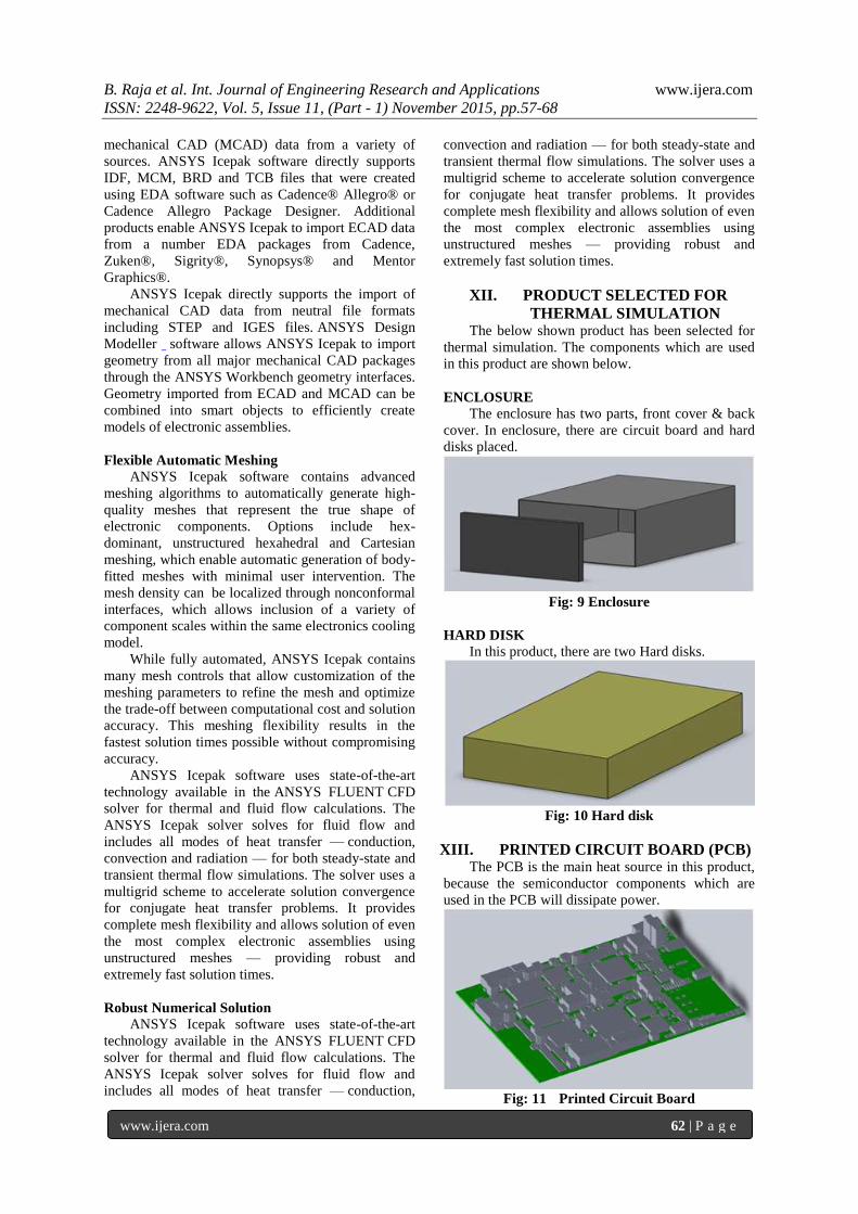
ENCLOSURE The enclosure has two parts, front cover & back
cover. In enclosure, there are circuit board and hard
disks placed.
Fig: 9 Enclosure
HARD DISK In this product, there are two Hard disks.
Fig: 10 Hard disk
XIII. PRINTED CIRCUIT BOARD (PCB) The PCB is the main heat source in this product,
because the semiconductor components which are
used in the PCB will dissipate power.
Fig: 11 Printed Circuit Board

B. Raja et al. Int. Journal of Engineering Research and Applications www.ijera.com
ISSN: 2248-9622, Vol. 5, Issue 11, (Part - 1) November 2015, pp.57-68
www.ijera.com 63 | P a g e
XIV. ASSEMBLY OF PARTS The parts are assembled inside the enclosure, the
assembly is made like actual product.
Fig: 12 Assembly of parts
XV. COMPONENTS CONSIDERED
FOR SIMULATION In the PCB there are many components. But
some components will generate heat because it will
consume more power. The selected components are
mentioned below.
Fig: 13 Components List
XVI. POWER DISSIPATION AND
TEMPERATURE LIMITS The power dissipation values are taken from the
datasheets of individual components and listed in the
below table. The maximum junction temperature of
the components which can withstand when operating
is listed in the table. If the component exceeds the
prescribed junction temperature, then the particular
device will get fail.
TABLE 3
POWER AND TEMPERATURE LIMIT CHART
Sl.
No Components
Power
in W
Temperature
Limit in °C
1 U1 49.2 125
2 U72 27.76 125
3 U73 27.76 125
4 U74 27.76 125
5 U99 2.5 125
6 U100 2.5 125
7 U85 0.435 85
8 U86 0.435 85
9 U75 0.435 85
10 U77 0.435 85
11 U90 0.435 85
12 U76 0.435 85
13 U78 0.435 85
14 U91 0.435 85
15 U93 0.435 85
16 U94 14.25 125
17 U34 17 125
XVII. THERMAL RESISTANCE VALUES TABLE 4
Thermal resistance values
Sl.N
o
Components Power
in W
Rjc
in
°C/W
Rjb in
°C/W
1 U1 49.2 0.1 3.5 2 U72 27.76 0.1 3.5
3 U73 27.76 0.1 3.5
4 U74 27.76 0.1 3.5
5 U99 2.5 10.1 31.19
6 U100 2.5 10.1 31.19
7 U85 0.435 4.4 10.44 8 U86 0.435 4.4 10.44
9 U75 0.435 4.4 10.44
10 U77 0.435 4.4 10.44
11 U90 0.435 4.4 10.44 12 U76 0.435 4.4 10.44 13 U78 0.435 4.4 10.44
14 U91 0.435 4.4 10.44
15 U93 0.435 4.4 10.44
16 U94 14.25 64.8 14.4 17 U34 17 64.8 14.4
XVIII. THERMAL SIMULATION PCB Level thermal simulation in natural
convection In this simulation, the PCB is kept in open
environment. The simulation is done in natural
convection mode. The calculated power dissipation &
resistance values are fed into the individual model.
The Total PCB thermal model is done in Ansys
IcePak tool as shown below.

B. Raja et al. Int. Journal of Engineering Research and Applications www.ijera.com
ISSN: 2248-9622, Vol. 5, Issue 11, (Part - 1) November 2015, pp.57-68
www.ijera.com 64 | P a g e
Fig: 14 PCB Thermal model
Fig: 15 Thermal Model with Meshing
TABLE 5
PCB LEVEL THERMAL SIMULATION RESULT
Sl.
No
Componen
ts
Simulated
Temperatu
re in °C
Temperatur
e Limit in °C
1 BOARD 138.456
2 U1 213.634 125
3 U72 141.428 125
4 U73 314.383 125
5 U74 212.15 125
6 U99 208.221 125
7 U100 209.885 85
8 U85 130.16 85
9 U86 129.921 85
10 U75 141.301 85
11 U77 147.715 85
12 U90 119.734 85
13 U76 128.535 85
14 U78 116.812 85
15 U91 118.567 85
16 U93 134.426 85
17 U94 237.051 125
18 U34 132.931 125
Fig: 16 Contours of PCB Level simulation Result
NOTE
According to the simulation result, all the
components exceeded maximum Junction
temperature limit. So the product failed.
System Level thermal simulation in natural
convection
The PCB and the hard disks are placed inside the
enclosure and done the system level thermal
simulation in natural convection.
TABLE 6
RESULTS OF SYSTEM LEVEL THERMAL SIMULATION
IN NATURAL CONVECTION
Sl.
No
Componen
ts
Simulated
Temperatu
re in °C
Temperatur
e Limit in
°C
1 BOARD 144.85
2 U1 226.206 125
3 U72 196.979 125
4 U73 469.124 125
5 U74 257.366 125

B. Raja et al. Int. Journal of Engineering Research and Applications www.ijera.com
ISSN: 2248-9622, Vol. 5, Issue 11, (Part - 1) November 2015, pp.57-68
www.ijera.com 65 | P a g e
6 U99 248.233 125
7 U100 250.11 85
8 U85 113.508 85
9 U86 122.17 85
10 U75 162.645 85
11 U77 212.444 85
12 U90 109.589 85
13 U76 107.837 85
14 U78 107.564 85
15 U91 107.577 85
16 U93 121.133 85
17 U94 340.369 125
18 U34 179.358 125
NOTE According to the system level Simulation result,
all the components are exceeded maximum Junction
temperature limit. So the product failed.
XIX. PRODUCT ENHANCEMENT Iteration 1
Since there is no air circulation inside the
enclosure, the product got failed in previous
simulation. So we modified the enclosure to have
better air for better convection heat transfer. The
modified model is shown below.
Fig: 17 Thermal Simulation in Natural
Convection
In the above shown model, vent holes are
provided on front and back cover of the product.
TABLE 7
RESULT WITH VENT HOLES SETUP IN NATURAL
CONVECTION
Sl.
No
Component
s
Simulated
Temperatu
re in °C
Temperature
Limit in °C
1 BOARD 124.565
2 U1 231.989 125
3 U72 159.369 125
4 U73 409.913 125
5 U74 261.046 125
6 U99 253.023 125
7 U100 255.344 85
8 U85 97.5216 85
9 U86 108.352 85
10 U75 169.31 85
11 U77 208.172 85
12 U90 72.4817 85
13 U76 75.417 85
14 U78 69.5815 85
15 U91 71.2659 85
16 U93 104.618 85
17 U94 267.461 125
18 U34 144.834 125
19 Hard disk1 168.542
20 Hard disk2 171.47
NOTE According to first iteration, some of the
components worked out and many of the components
got failed.
Inputs for Fan Selection
Fig: 18 Model with fan Table
TABLE 8
Results on thermal simulation with forced
convection
Sl.
No
Compon
ents
Simulated
Temperature
in °C
Temperatur
e Limit in
°C
1 BOARD 122.873
2 U1 226.304 125
3 U72 157.685 125
4 U73 275.192 125
5 U74 248.631 125
6 U99 243.018 125
7 U100 239.553 85
8 U85 115.799 85
9 U86 121.94 85
10 U75 155.888 85
11 U77 166.916 85
12 U90 85.6956 85
13 U76 103.237 85
14 U78 87.9969 85
15 U91 89.5494 85
16 U93 115.029 85
17 U94 284.436 125
18 U34 137.849 125

B. Raja et al. Int. Journal of Engineering Research and Applications www.ijera.com
ISSN: 2248-9622, Vol. 5, Issue 11, (Part - 1) November 2015, pp.57-68
www.ijera.com 66 | P a g e
Fig: 19 Contours forced convection simulation
result
Fig: 20 Air flow
NOTE According to the forced convection results, all
the components failed.
Iteration 2 Since the area of contact is more inside the
product, the sucked air is not passing through the
components.
In this iteration we are planning to reduce the area
of the enclosure near to the PCB, because the
majority of air circulated above the PCB which was
not required. So we decided to redirect the air flow
towards the PCB by introducing a Baffle Plate and
modifying the vent holes on top surface of the
enclosure. The hard disk location also got changed
due to space constrain to place the Baffle Plate. The
modified product setup is shown below.
Fig: 21 Baffle plate attached
TABLE 9
Simulation result on forced convection with baffle
plate
Sl.
No
Componen
ts
Simulated
Temperatu
re in °C
Temperature
Limit in °C
1 BOARD 87.6197
2 U1 161.578 125
3 U72 104.616 125
4 U73 155.081 125
5 U74 140.965 125
6 U99 137.714 125
7 U100 140.712 85
8 U85 90.6301 85
9 U86 86.8725 85
10 U75 93.5949 85
11 U77 93.2014 85
12 U90 87.0362 85
13 U76 92.7542 85
14 U78 81.1759 85
15 U91 78.7009 85
16 U93 85.2573 85
17 U94 219.218 125
18 U34 97.7462 125
19 Hard disk1 30.506
20 Hard disk2 26.3746
Fig: 22 Simulation result for forced convection

B. Raja et al. Int. Journal of Engineering Research and Applications www.ijera.com
ISSN: 2248-9622, Vol. 5, Issue 11, (Part - 1) November 2015, pp.57-68
www.ijera.com 67 | P a g e
Fig: 23 Air flow through exhaust fan
NOTE According to Iteration 2 some of the components
worked out and all other components are very close
to maximum limits.
Iteration 3 In the previous iteration majority of the
components were close to the pass region. Due to the
high power dissipation components, the other
components are in failure region. So heat sinks with
fins are fixed to dissipate heat through conduction
from hot components. The heat sink can be decided
as per below process.
Inputs for Heat Sink Selection
Power dissipation of the chip set / processor
(Pmax)
Maximum allowable junction temperature (TJ) or
Case Temperature
Thermal resistances, RJC, RCA and RJB
Local ambient Temperature (TA)
Form factor of the system
Space availability
Flow availability
Chip or processor mechanical requirements
(weight and mounting arrangement)
Selection Procedure
Calculation of Thermal Resistance: Thermal resistance of the heat sink (Heat sink to
Ambient) will be calculated as follows
RSA = (TJ-TA ) / Pmax-RJC - RTIM (Here
RTIM=Thermal Interface material resistance)
TABLE 10
SIMULATION RESULTS
Sl.
No Components
Simulated
Temperature
in °C
Temperature
Limit in °C
1 BOARD 53.3359
2 U1 77.9133 125
3 U72 78.1164 125
4 U73 112.373 125
5 U74 71.8405 125
6 U99 68.2758 125
7 U100 71.5518 85
8 U85 59.1115 85
9 U86 56.9832 85
10 U75 60.0849 85
11 U77 59.5009 85
12 U90 58.9298 85
13 U76 59.843 85
14 U78 54.5763 85
15 U91 51.8815 85
16 U93 55.5079 85
17 U94 124.691 125
18 U34 72.4292 125
19 Hard disk1 22.4728
20 Hard disk2 21.1395
TABLE 11
COMPARISON BETWEEN PRE ENHANCEMENT AND
POST ENHANCEMENT
Sl.
N
o
Compo
nents
Initial
Design
Results
Temperat
ure in °C
Enhanced
Design
Results
Temperat
ure in °C
Tempe
rature
Limit
in °C
1 BOARD 144.85 53.3359
2 U1 226.206 77.9133 125
3 U72 196.979 78.1164 125
4 U73 469.124 112.373 125
5 U74 257.366 71.8405 125
6 U99 248.233 68.2758 125
7 U100 250.11 71.5518 85
8 U85 113.508 59.1115 85
9 U86 122.17 56.9832 85
10 U75 162.645 60.0849 85
11 U77 212.444 59.5009 85
12 U90 109.589 58.9298 85
13 U76 107.837 59.843 85
14 U78 107.564 54.5763 85
15 U91 107.577 51.8815 85
16 U93 121.133 55.5079 85
17 U94 340.369 124.691 125
18 U34 179.358 72.4292 125
19 Hard
disk1
186.076 22.4728
20 Hard
disk2
180.79 21.1395
Fig: 24 Air flow through Exhaust Fan

B. Raja et al. Int. Journal of Engineering Research and Applications www.ijera.com
ISSN: 2248-9622, Vol. 5, Issue 11, (Part - 1) November 2015, pp.57-68
www.ijera.com 68 | P a g e
Fig: 25 Pressure inside the product
NOTE According to Iteration 3, all the components
operating temperature are within the maximum limit.
XX. CONCLUSION The post enhancement result works well than the
pre enhancement result. The operating temperature
values are within the maximum limit in iteration 3,
hence the life of product much improved. The rate of
failure on components is very less, so the reliability
of the product improved and cost on service also
reduced.
The same process can be followed to any
electronic product for better thermal performance.
REFERENCE
[1] Annual IEEE Semiconductor Thermal
Measurement and Management Symposium-
3105; 2208.
[2] Applied Thermal Engineering-2102; 2209.
[3] Experimental Thermal and Fluid Science-
1500; 2210; 2104; 1507; 2202.
[4] Handbook of Thermal Analysis and
Calorimetry-2500; 3107.
[5] International Journal of Thermal Sciences-
2200; 3104.
[6] Journal of Thermal Science and
Technology-3107; 2200.
[7] Journal of Thermal Analysis-2200.
[8] Journal of Thermal Analysis and
Calorimetry-1606; 3104.
[9] Journal of Thermo physics and Heat
Transfer-3104.
[10] JSME International Journal, Series B: Fluids
and Thermal. Engineering2210; 1606; 1507.
[11] LearnCAx


