PUBLIC
APPLICATIONS ENGINEERING
TIPS FOR SILICON BRING-UP OF QORIQ LS1
PROCESSOR FAMILY
PUBLIC 1
Agenda
• Chip Feature comparison
• Interface specific compatibility
− Clocking
− DDR
− IFC
− Boot Sources
− SerDes
− Other
• Board Design Phase
− Design Considerations
• Pre-Boot Phase
− RCW
− DDR Validation
• SDK Phase
− Introduction
− Build
− Deployment
• Final Phase: Board Boot Up and
Beyond ….
PUBLIC 2
Introduction
• Intended Audience
− Hardware and software engineers bringing up new boards based on NXP QorIQ LS
Family
• Key feature comparison and consideration for common board design for
LS1043/LS1046/LS1088
• Brief introduction to pre-boot requirements
• Board debug and validation
• Software development for silicon enablement
PUBLIC 3
Assumptions
• NOR flash is primary boot location
− location for RCW, bootloader, Linux
• Bootloader relocates to DDR after initial execution
• Primary Core: Core0
• NXP debug tools used: CodeWarrior, CodeWarriorTAP
• NXP software used: NXP SDK
• No Secure Boot
• Attendees have prior silicon bring up experience

PUBLIC 4
Frequently Used Acronyms
IFC Integrated Flash Controller
DDR Double Data Rate
(interchangeably used with DDR)
DDRv DDR Validation Tool
LS LayerScape
PBI Pre-Boot Initialization
PBL Pre-Boot Loader
QCVS QorIQ Configuration and Validation Suite
RCW Reset Configuration Word
SDK Software Development Kit
PUBLIC 5
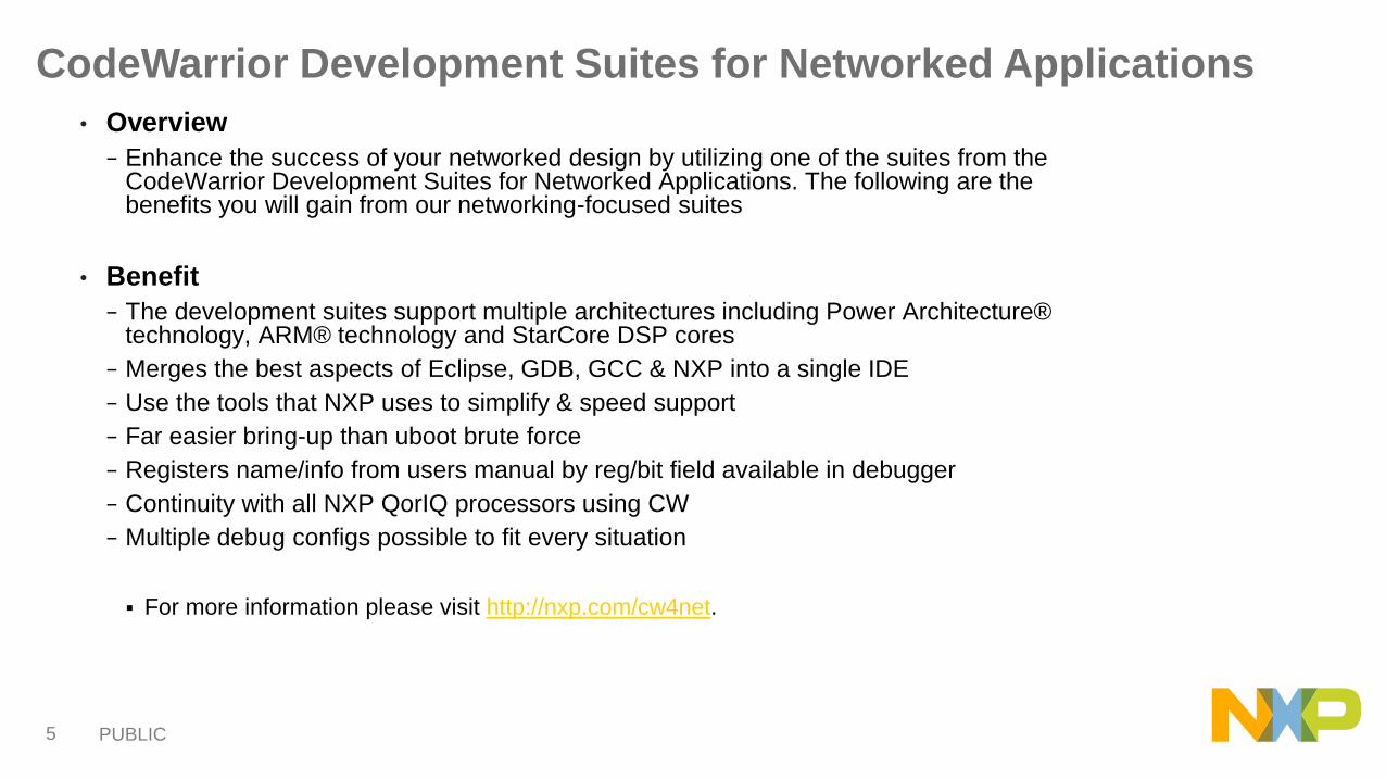
CodeWarrior Development Suites for Networked Applications
• Overview
− Enhance the success of your networked design by utilizing one of the suites from the CodeWarrior Development Suites for Networked Applications. The following are the benefits you will gain from our networking-focused suites
• Benefit
− The development suites support multiple architectures including Power Architecture® technology, ARM® technology and StarCore DSP cores
− Merges the best aspects of Eclipse, GDB, GCC & NXP into a single IDE
− Use the tools that NXP uses to simplify & speed support
− Far easier bring-up than uboot brute force
− Registers name/info from users manual by reg/bit field available in debugger
− Continuity with all NXP QorIQ processors using CW
− Multiple debug configs possible to fit every situation
For more information please visit http://nxp.com/cw4net.

PUBLIC 6
CHIP FEATURE COMPARISON
PUBLIC 7
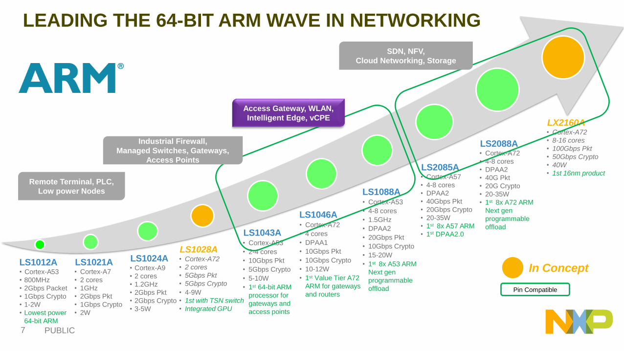
LS1012A• Cortex-A53
• 800MHz
• 2Gbps Packet
• 1Gbps Crypto
• 1-2W
• Lowest power
64-bit ARM
LS1021A• Cortex-A7
• 2 cores
• 1GHz
• 2Gbps Pkt
• 1Gbps Crypto
• 2W
LS2085A• Cortex-A57
• 4-8 cores
• DPAA2
• 40Gbps Pkt
• 20Gbps Crypto
• 20-35W
• 1st 8x A57 ARM
• 1st DPAA2.0LS1043A• Cortex-A53
• 2-4 cores
• 10Gbps Pkt
• 5Gbps Crypto
• 5-10W
• 1st 64-bit ARM
processor for
gateways and
access points
LS1088A• Cortex-A53
• 4-8 cores
• 1.5GHz
• DPAA2
• 20Gbps Pkt
• 10Gbps Crypto
• 15-20W
• 1st 8x A53 ARM
Next gen
programmable
offload
LS1046A• Cortex-A72
• 4 cores
• DPAA1
• 10Gbps Pkt
• 10Gbps Crypto
• 10-12W
• 1st Value Tier A72
ARM for gateways
and routers
LS1024A• Cortex-A9
• 2 cores
• 1.2GHz
• 2Gbps Pkt
• 2Gbps Crypto
• 3-5W
LS2088A• Cortex-A72
• 4-8 cores
• DPAA2
• 40G Pkt
• 20G Crypto
• 20-35W
• 1st 8x A72 ARM
Next gen
programmable
offload
LX2160A• Cortex-A72
• 8-16 cores
• 100Gbps Pkt
• 50Gbps Crypto
• 40W
• 1st 16nm product
Remote Terminal, PLC,
Low power Nodes
LS1028A• Cortex-A72
• 2 cores
• 5Gbps Pkt
• 5Gbps Crypto
• 4-9W
• 1st with TSN switch
• Integrated GPU
LEADING THE 64-BIT ARM WAVE IN NETWORKING
In Concept
Pin Compatible
Industrial Firewall,
Managed Switches, Gateways,
Access Points
SDN, NFV,
Cloud Networking, Storage
Access Gateway, WLAN,
Intelligent Edge, vCPE

PUBLIC 8
Core complex
1x 64-bit Cortex-A53 with Neon SIMD engine
Speed up to 800 MHz
Parity-protected 32 KB L1 instruction and 32 KB L1 data
cache
256 KB L2 cache with ECC protection
Basic peripheral and Interconnect
1x USB 3.0/2.0 controller with integrated PHY
1x USB 2.0 controller with ULPI
2x eSDHC controllers supporting SD 3.0, eMMC 4.4 and
eMMC 4.5 modes
Five SAI supporting I2S
Networking elements
2x quad-speed Ethernet MACs supporting 2.5G, 1G,
100M, 10M
Supports RGMII, SGMII 1G, SGMII 2.5G
Up to 2 x SGMII supporting 1 or 2.5 Gbps
1x PCI Express Gen 2 controller
1x SATA Gen 3.0 controller
Accelerators and Memory Control
1x 16-bit DDR3L Controller up to 1.0 GT/s
Security Engine (SEC)
QorIQ Trust architecture: Secure boot, ARM Trust zone
and security monitor
Qualification
Commercial and extended
temperature
LS1012A: First 64-bit single core ARM Cortex A53 ProcessorWorld’s lowest power 64-bit ARM based processor
Trust-enabled IoT Gateways
Consumer NAS
Mobile NAS
Ethernet drives for data center storage
Entry-level broadband Ethernet
gateways
Building and Factory automation
Target Applications Development platforms:• LS1012A-RDB• FRDM-LS1012A

PUBLIC 9
LS1026/46A: Dual/Quad ARM Cortex A72 ProcessorHigh Performance SoC for Virtualization
• Enterprise routers and switches• Linecard controllers• Network attached storage• Security appliances
• Virtual customer premise equipment (vCPE)
• Service provider gateways• Single board computers
Target Applications:
Core complex 4x 32/64-bit Cortex-A72 with Neon SIMD engine
Speed up to 1800 MHz
Parity and ECC protected 48 KB L1 instruction and 32
KB L1 data cache
2 MB L2 cache with ECC protection
Basic peripheral and Interconnect 3x USB 3.0 controllers with integrated PHY
1x eSDXC controllers supporting SD 3.0, and eMMC 4.5
modes
Networking elements Packet parsing, classification, and distribution
Queue Management for scheduling, packet sequencing
and congestion management
Hardware buffer management for buffer allocation and
de-allocation
Up to five SGMII supporting 1 Gbps
Up to three SGMII supporting 2.5 Gbps
Up to two XFI supporting 10 Gbps
Up to one QSGMII
3x PCI Express Gen 3 controller
1x SATA Gen 3.0 controller
Accelerators and Memory Control 1x 32-bit DDR4 Controller with ECC support up to 2.1
GT/s
Security Engine (SEC)
QorIQ Trust architecture: Secure boot, ARM Trust zone
and security monitor
Qualification Commercial and extended
temperature
Development platforms:• LS1046A-RDB

PUBLIC 10
LS1043A
Datapath Acceleration
• SEC- crypto acceleration
• L2/3 & Custom Classification
• Tunnel Header Offload
• Reassembly
• Traffic Management & Shaping
Processor
• 4x A53, 64b, up to 1.6GHz
• 1MB L2 cache shared by all cores (and platform
elements)
Memory Subsystem
• 32b DDR3L/4 Controller with ECC up to 1600MHz
CCI-400 Switch Fabric
• Advanced VM hardware support
High Speed Serial IO
• 3x PCIe Gen2 Controllers
• 1x SATA 3.0
• 3x USB 3.0 with PHY
Network IO
• 1x10G; 1x QSGMII; 2x 2.5G SGMII; 4x 1G SGMII; 2x
RGMII
• Proven Packet Parse/Classify/Distribute
• Up to 2.5Gbps IMIX
• IPSec, GRE, CAPWAP, DTLS Offload
• Lossless Flow Control
Device
• 28HPM Process
• 21x21 mm, 621 FC-PBGA, 0.8mm pitch
• 23x23 mm, 780 FC-PBGA, 0.8mm pitch

PUBLIC 11
General Purpose Processing Layer
• 4 or 8 x ARM A53 CPUs, 64b, 1.6GHz
• 1MB L2 cache/ cluster
• HW L1 & L2 Prefetch Engines
• Neon SIMD in all CPUs
Memory Subsystem
• 64b DDR4 up to 2.1GT/s
CCI-400 Switch Fabric
• Advanced VM hardware support
Advanced I/O Processor
• Programmable packet handling
High Speed I/O
• 3x PCIe Gen3 controllers
• SATA 3.0, 2 x USB 3.0 with PHYs
Network I/O
• 2x 10GbE + 8x1G
• 2x10G; 2x QSGMII; 2x 2.5G SGMII; 4x 1G SGMII; 2x RGMII
• XFI/KR and SGMII/KX
• MACSec on up to 4x 1GbE
• uQE for HDLC, T1/E1 support
Industrial connectivity
• Ethernet, Serial (RS485/422), uQE (for additional serial fieldbus apps)
Device
• 28HPM Process
• 23x23 mm, 780 FC-PBGA, 0.8mm pitch
Security
• Hardware – Encryption (IPSec)
• Secure Boot
• Trust Zone & Trust Architecture
• MACSec support
LS1088A
PUBLIC 12
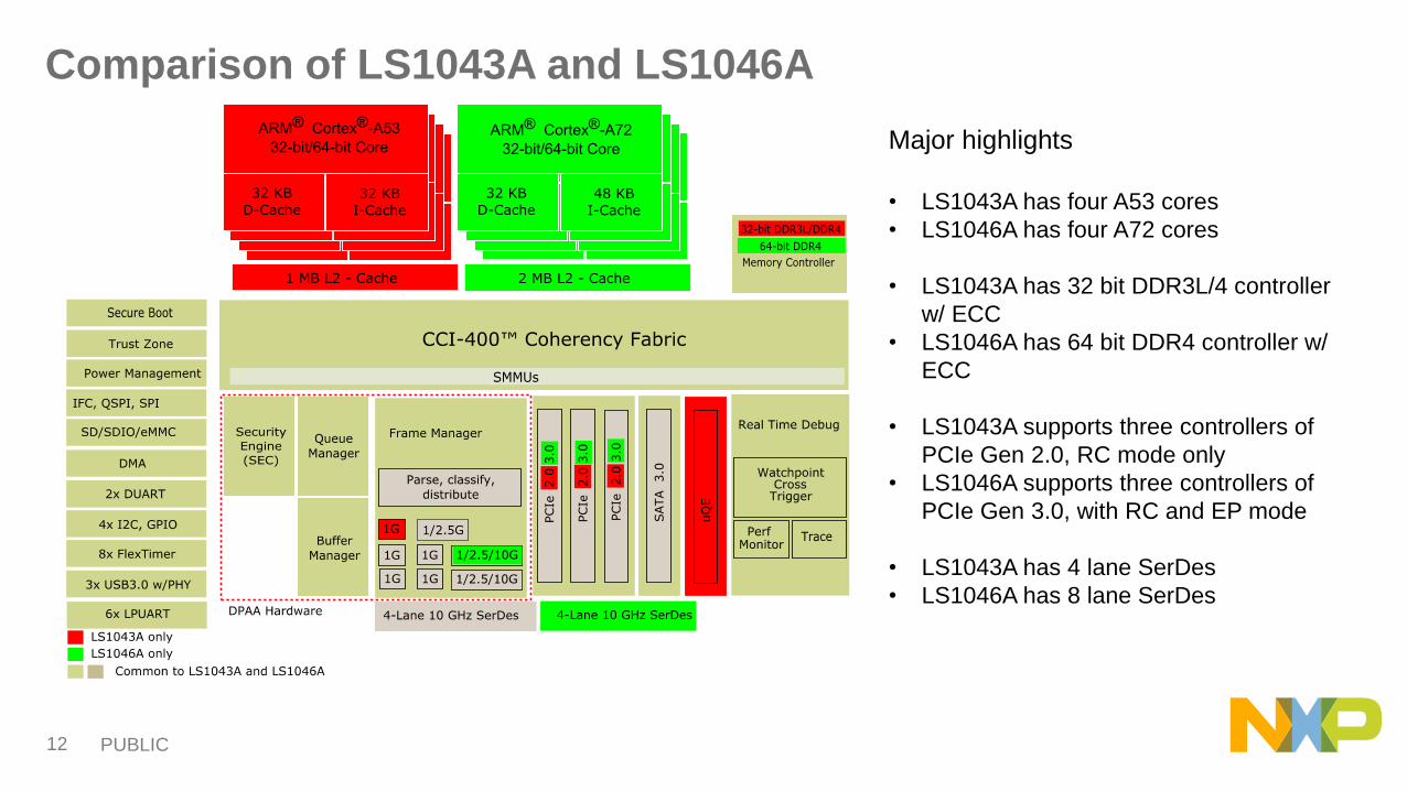
Comparison of LS1043A and LS1046A
Major highlights
• LS1043A has four A53 cores
• LS1046A has four A72 cores
• LS1043A has 32 bit DDR3L/4 controller
w/ ECC
• LS1046A has 64 bit DDR4 controller w/
ECC
• LS1043A supports three controllers of
PCIe Gen 2.0, RC mode only
• LS1046A supports three controllers of
PCIe Gen 3.0, with RC and EP mode
• LS1043A has 4 lane SerDes
• LS1046A has 8 lane SerDes
PUBLIC 13
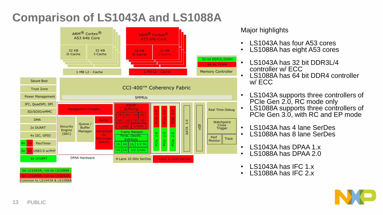
Comparison of LS1043A and LS1088AMajor highlights
• LS1043A has four A53 cores• LS1088A has eight A53 cores
• LS1043A has 32 bit DDR3L/4 controller w/ ECC
• LS1088A has 64 bit DDR4 controller w/ ECC
• LS1043A supports three controllers of PCIe Gen 2.0, RC mode only
• LS1088A supports three controllers of PCIe Gen 3.0, with RC and EP mode
• LS1043A has 4 lane SerDes• LS1088A has 8 lane SerDes
• LS1043A has DPAA 1.x• LS1088A has DPAA 2.0
• LS1043A has IFC 1.x• LS1088A has IFC 2.x
PUBLIC 14
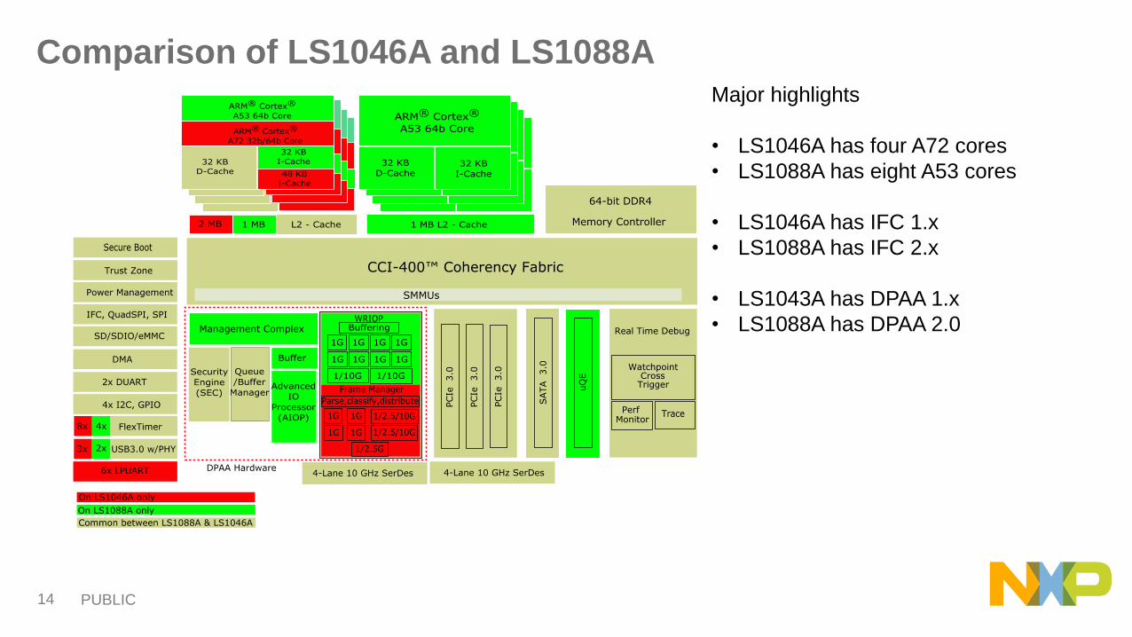
Comparison of LS1046A and LS1088AMajor highlights
• LS1046A has four A72 cores
• LS1088A has eight A53 cores
• LS1046A has IFC 1.x
• LS1088A has IFC 2.x
• LS1043A has DPAA 1.x
• LS1088A has DPAA 2.0

PUBLIC 15
BOARD DESIGN PHASE
PUBLIC 16
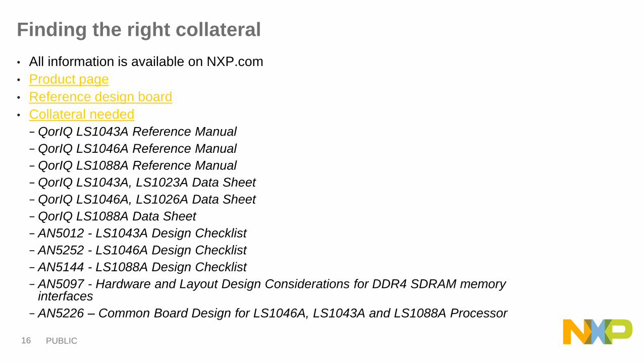
Finding the right collateral
• All information is available on NXP.com
• Product page
• Reference design board
• Collateral needed
− QorIQ LS1043A Reference Manual
− QorIQ LS1046A Reference Manual
− QorIQ LS1088A Reference Manual
− QorIQ LS1043A, LS1023A Data Sheet
− QorIQ LS1046A, LS1026A Data Sheet
− QorIQ LS1088A Data Sheet
− AN5012 - LS1043A Design Checklist
− AN5252 - LS1046A Design Checklist
− AN5144 - LS1088A Design Checklist
− AN5097 - Hardware and Layout Design Considerations for DDR4 SDRAM memory interfaces
− AN5226 – Common Board Design for LS1046A, LS1043A and LS1088A Processor

PUBLIC 17
Design Considerations
• Power supply requirements
• Boot source
− IFC: NOR Flash, NAND Flash
− QSPI
− eSDHC/MMC
• Using CPLD/FPGA for reset and signal routing
− Reset_req_b to be connected to FPGA/CPLD
• Clock sources
− SYSCLK and DDRCLK must always be driven
− ECn_GTX_CLK125 must be driven if RGMII mode is used on the respective ECn port
− SerDes reference clocks (SDn_REF_CLKn and SDn_REF_CLKn_B) must be driven if the corresponding SerDes bank is enabled in the RCW
− Optional input clock sources include RTC, USBCLK, and TSEC_1588_CLK_IN

PUBLIC 18
PRE-BOOT PHASE

PUBLIC 19
PORESET Signals
• Various chip functions are initialized by sampling certain
signals during the assertion of PORESET_B.
• These power-on reset (POR) inputs are pulled either high or
low during this period.
• While these pins are generally output pins during normal
operation, they are treated as inputs while PORESET_B is
asserted.
SoC
External logic
CPLD/FPGA
PORESET_BRESET_REQ_B
PUBLIC 20
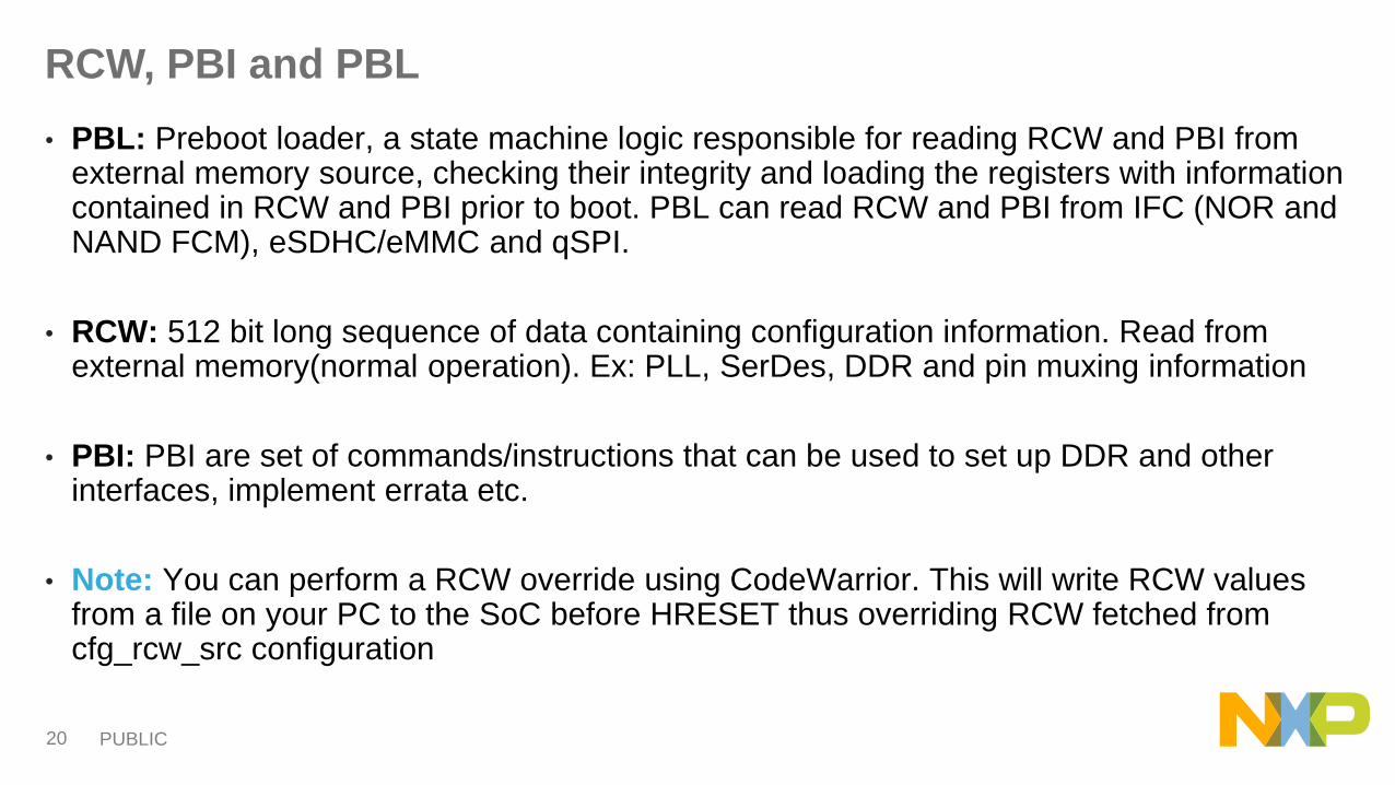
RCW, PBI and PBL
• PBL: Preboot loader, a state machine logic responsible for reading RCW and PBI from external memory source, checking their integrity and loading the registers with information contained in RCW and PBI prior to boot. PBL can read RCW and PBI from IFC (NOR and NAND FCM), eSDHC/eMMC and qSPI.
• RCW: 512 bit long sequence of data containing configuration information. Read from external memory(normal operation). Ex: PLL, SerDes, DDR and pin muxing information
• PBI: PBI are set of commands/instructions that can be used to set up DDR and other interfaces, implement errata etc.
• Note: You can perform a RCW override using CodeWarrior. This will write RCW values from a file on your PC to the SoC before HRESET thus overriding RCW fetched from cfg_rcw_src configuration
PUBLIC 21
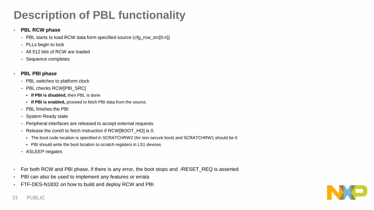
Description of PBL functionality• PBL RCW phase
− PBL starts to load RCW data form specified source (cfg_rcw_src[0:n])
− PLLs begin to lock
− All 512 bits of RCW are loaded
− Sequence completes
• PBL PBI phase
− PBL switches to platform clock
− PBL checks RCW[PBI_SRC]
If PBI is disabled, then PBL is done
If PBI is enabled, proceed to fetch PBI data from the source.
− PBL finishes the PBI
− System Ready state
− Peripheral interfaces are released to accept external requests
− Release the core0 to fetch instruction if RCW[BOOT_HO] is 0.
The boot code location is specified in SCRATCHRW2 (for non-secure boot) and SCRATCHRW1 should be 0
PBI should write the boot location to scratch registers in LS1 devices
− ASLEEP negates
• For both RCW and PBI phase, if there is any error, the boot stops and /RESET_REQ is asserted
• PBI can also be used to implement any features or errata
• FTF-DES-N1832 on how to build and deploy RCW and PBI
PUBLIC 22
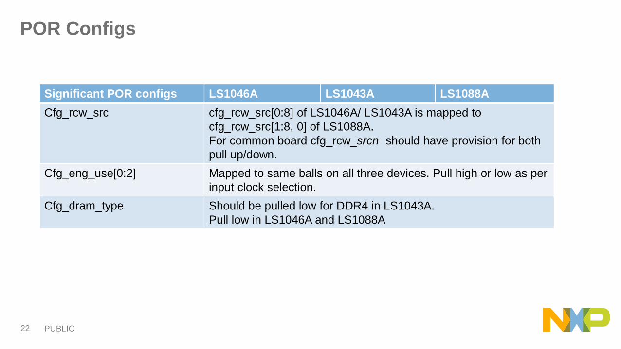
POR Configs
Significant POR configs LS1046A LS1043A LS1088A
Cfg_rcw_src cfg_rcw_src[0:8] of LS1046A/ LS1043A is mapped to
cfg_rcw_src[1:8, 0] of LS1088A.
For common board cfg_rcw_srcn should have provision for both
pull up/down.
Cfg_eng_use[0:2] Mapped to same balls on all three devices. Pull high or low as per
input clock selection.
Cfg_dram_type Should be pulled low for DDR4 in LS1043A.
Pull low in LS1046A and LS1088A

PUBLIC 23
Boot Sources
Boot Sources LS1046A LS1043A LS1088A Remarks
NOR Flash memory (8 bit) ×
NOR Flash memory (16 bit) 16 bit NOR flash is not pin compatible
across the three devices, it will require
a complex on board logic to provision
booting.
NAND Flash Memory × × Booting from NAND device is not
supported on LS1046A and LS1088A
SD/eMMC Fully compatible
QSPI Fully compatible
Since only 8 bit NAND interface is pin compatible, hence no IFC boot mechanism is common across the three devices. It is recommended to use SD/eMMC or QSPI as boot source and storage device on the common board. However if a common board is designed to support LS1043A and LS1046A only, IFC NOR may be considered.
PUBLIC 24
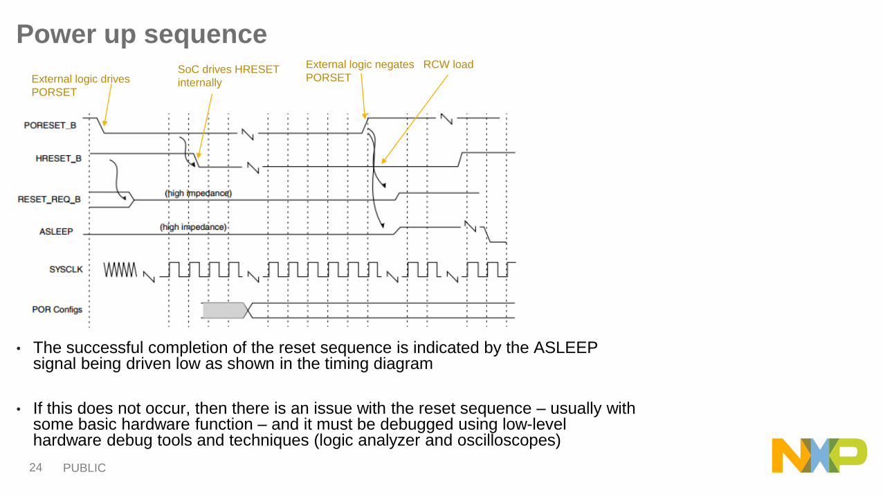
Power up sequence
• The successful completion of the reset sequence is indicated by the ASLEEP signal being driven low as shown in the timing diagram
• If this does not occur, then there is an issue with the reset sequence – usually with some basic hardware function – and it must be debugged using low-level hardware debug tools and techniques (logic analyzer and oscilloscopes)
External logic drives
PORSET
SoC drives HRESET
internally
External logic negates
PORSET
RCW load
PUBLIC 25
Power up Sequence (continued)• Things to check if the Power up sequence does not complete include:
− Voltage Rails: Ensure the all the required voltage levels are provided and meet the
specified levels and tolerances
Ensure that the recommended power rail sequence is followed
− SYSCLK: Ensure it is present and meets the voltage level, slew rate, frequency, duty cycle, and jitter requirements
specified
− Reset Signals: Ensure PORESET is driven for a minimum of 1 ms and that it is driven
before the core and platform voltages are powered up
If HRESET is driven externally, ensure it is released as expected; if driven just by the SoC, confirm
it is released after PORESET desertion
− Confirm the RCW device is being read after ASLEEP is driven high
If not, check that the cfg_rcw_src signals are driven as expected when the PORESET signal is released
− Confirm RCW contents are as expected. The specifics of the RCW must match the system configuration
− If the RCW device is blank, a tool such as CodeWarrior must be used to program this. Instructions for doing this are provided in later
in another session. However, it is recommended to confirm the hardware operation as much as possible before connecting this tool.
Confirming that the LS1043A at least attempts to read the RCW device is a good checkpoint
− Also good to have a mechanism like a switch, that can stop external logic to assert PORESET on assertion of RESET_REQ by SoC

PUBLIC 26
CLOCKING DIFFERENCES

PUBLIC 27
Clocking - Single source clocking scheme as in LS1088A
The Differential SYSCLK clock input can feed Core PLLs, Platform PLL, DDR PLL and USB PLL .
Additionally it can be used to feed the four SerDes PLL, selectable option through RCW bits 952, 953, 954 and 955

PUBLIC 28
Clocking - Single source clocking scheme as in LS1043A
The Differential SYSCLK clock input can feed Core PLLs, Platform PLL,
DDR PLL and USB PLL .
The two SerDes PLL require individual clock inputs from board.

PUBLIC 29
Clocking - Single source clocking scheme as in LS1046A
The Differential SYSCLK clock input can feed Core PLLs, Platform PLL, DDR PLL and USB PLL. SerDes PLL1 clock input can be used to clock the SerDes PLL2, selectable through RCW bits.

PUBLIC 30
SERDES
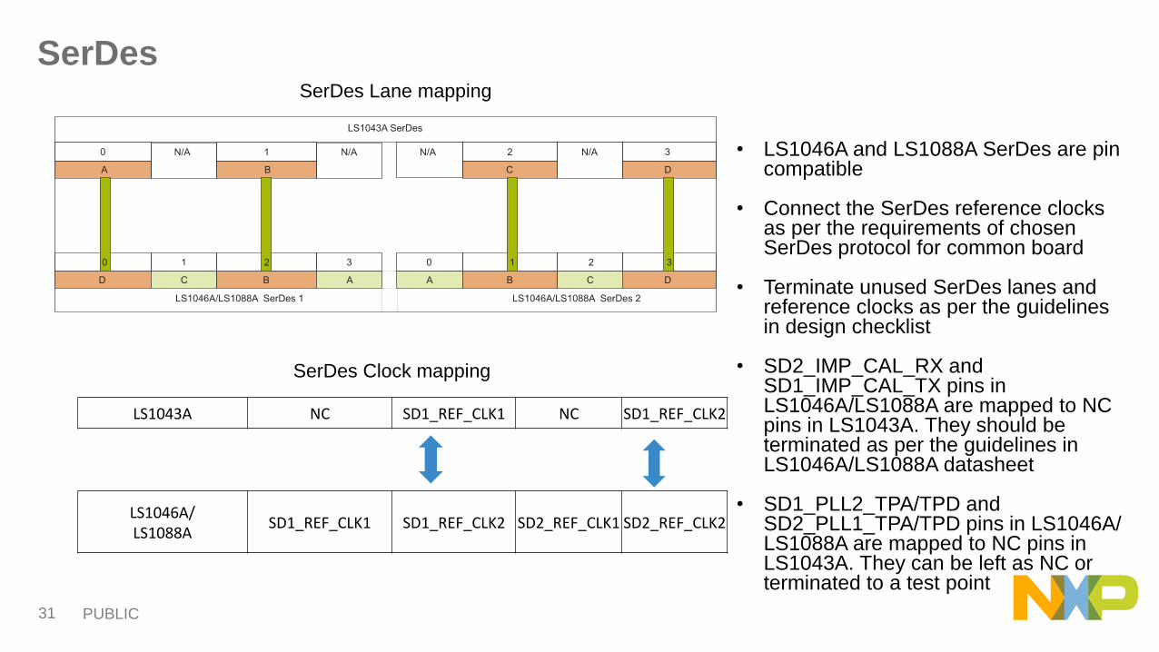
PUBLIC 31
LS1043A NC SD1_REF_CLK1 NC SD1_REF_CLK2
LS1046A/LS1088A
SD1_REF_CLK1 SD1_REF_CLK2 SD2_REF_CLK1 SD2_REF_CLK2
SerDes
• LS1046A and LS1088A SerDes are pin compatible
• Connect the SerDes reference clocks as per the requirements of chosen SerDes protocol for common board
• Terminate unused SerDes lanes and reference clocks as per the guidelines in design checklist
• SD2_IMP_CAL_RX and SD1_IMP_CAL_TX pins in LS1046A/LS1088A are mapped to NC pins in LS1043A. They should be terminated as per the guidelines in LS1046A/LS1088A datasheet
• SD1_PLL2_TPA/TPD and SD2_PLL1_TPA/TPD pins in LS1046A/ LS1088A are mapped to NC pins in LS1043A. They can be left as NC or terminated to a test point
SerDes Lane mapping
SerDes Clock mapping

PUBLIC 32
TOOLS
PUBLIC 33
CodeWarrior Debug
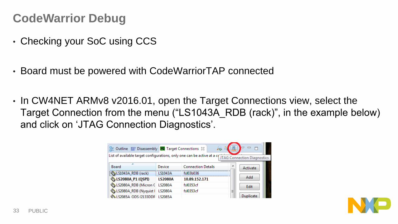
• Checking your SoC using CCS
• Board must be powered with CodeWarriorTAP connected
• In CW4NET ARMv8 v2016.01, open the Target Connections view, select the
Target Connection from the menu (“LS1043A_RDB (rack)”, in the example below)
and click on ‘JTAG Connection Diagnostics’.

PUBLIC 34
CodeWarrior Debug..contd..
• Clicking on any line of the report will display more information, if available. “Scan IDCODE” shown here.
• This is the recommended method for running JTAG diagnostics in CW ARMv8.
PUBLIC 35
CodeWarrior Debug contd..
• Create a RCW override file using information in the video link below
− http://www.nxp.com/video/how-to-create-a-rcw-override-configuration-file-for-use-in-a-
CodeWarrior-qoriq-debugger:RCW-QORIQ-DEBUGGER
• Use the RCW override file to override the RCW using CodeWarrior
− http://www.nxp.com/video/how-to-use-qoriq-rcw-override-feature-in-codewarrior:HOW-
TO-USE-QORIQ-RCW-CODEWARRIOR
• More details can be found in the User guide for CodeWarrior ARM v8
− http://cache.nxp.com/files/soft_dev_tools/doc/user_guide/CWARMv8TM.pdf?fpsp=1&WT
_TYPE=Users%20Guides&WT_VENDOR=FREESCALE&WT_FILE_FORMAT=pdf&WT_
ASSET=Documentation&fileExt=.pdf

PUBLIC 36
DDRv
• Allows configuration of DDR controller memory mapped (in CCSR) registers
• View DDR controller memory mapped registers on a bit field level
• Can read DDR configuration from various sources (memory dump, DIMM’s SPD, directly from target [in the making…])
• Generates DDR initialization code in various formats: uBoot data structure, plain C code, GDB script
• Exports DDR registers configuration dump to various formats
• Same advantages as PBL tool
− Same user experience across processors
− No need for reference manual
− Incorporates errata
− Validates input against known constraints
• DDR validation should be done before SDK phase so as to plug in the right DDR register settings for optimum and stable performance of DDR. Performing DDRv will eliminate border cases where certain boards work while others do not
PUBLIC 37
http://www.nxp.com/products/software-and-tools/software-development-tools/codewarrior-development-tools/suite-
for-networked-applications/qoriq-configuration-and-validation-suite:PE_QORIQ_SUITE#
PUBLIC 38
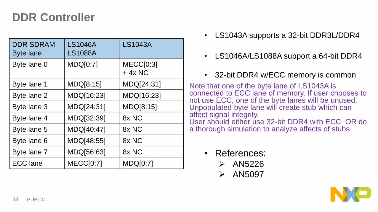
DDR Controller
• LS1043A supports a 32-bit DDR3L/DDR4
• LS1046A/LS1088A support a 64-bit DDR4
• 32-bit DDR4 w/ECC memory is common
• References: AN5226
AN5097
DDR SDRAM
Byte lane
LS1046A
LS1088A
LS1043A
Byte lane 0 MDQ[0:7] MECC[0:3]
+ 4x NC
Byte lane 1 MDQ[8:15] MDQ[24:31]
Byte lane 2 MDQ[16:23] MDQ[16:23]
Byte lane 3 MDQ[24:31] MDQ[8:15]
Byte lane 4 MDQ[32:39] 8x NC
Byte lane 5 MDQ[40:47] 8x NC
Byte lane 6 MDQ[48:55] 8x NC
Byte lane 7 MDQ[56:63] 8x NC
ECC lane MECC[0:7] MDQ[0:7]
Note that one of the byte lane of LS1043A is connected to ECC lane of memory. If user chooses to not use ECC, one of the byte lanes will be unused. Unpopulated byte lane will create stub which can affect signal integrity. User should either use 32-bit DDR4 with ECC OR do a thorough simulation to analyze affects of stubs
PUBLIC 39
SDK PHASE
Suggested sessions: FTF-DES-N1851,N1834,N1843
PUBLIC 40
Introduction to SDK
• Software development kit: Linux based dev kit
− Evaluate and explore SoC processors’ features
− Develop Linux-based solutions
• Contains
− boot loader: U-Boot
− Linux kernel
− user space components
− tool chain
− build system
− package manager
• Based on Yocto project and Poky
• More details can be found at http://www.nxp.com/knowledgecenter

PUBLIC 42
Using Pre-built Images
• Pre-built images for each SDK version are release in the IMAGE ISO
• Download SDK from www.nxp.com/sdk
• Download, mount and install IMAGE ISO
− $ sudo mount -o loop QorIQ-SDK-<version>-<target>-IMAGE-<yyyymmdd>-yocto.iso /mnt/cdrom
− For LS1043A: QorIQ-SDK-V2.0-AARCH64-IMAGE-20160527-yocto.iso
• Contains all images necessary to boot to Linux are available
PUBLIC 43
Download and install SDK
• Download SDK from www.nxp.com/sdk
• See “Getting Started with Yocto Project” Section on KnowledgeCenter
• Download, mount and install Source ISO
− For LS1043A: QorIQ-SDK-V2.0-SOURCE-20160527-yocto.iso
− $ sudo mount -o loop QorIQ-SDK-<version>-<target>-<yyyymmdd>-yocto.iso /mnt/cdrom
− As super user install “install” from /mnt/cdrom (./install)
• Download mount and install cache ISO (* The cache ISO contains the pre-built cache binaries)
− For LS1043A: QorIQ-SDK-V2.0-AARCH64-CACHE-20160527-yocto.iso
• Set up host environment according to Yocto project requirements
• Setup poky for specific board (Assuming we are setting up LS1043RDB)
− In the build directory execute the following command
− . ./fsl-setup-env -m <machine> (ex: . ./fsl-setup-env -m ls1043rdb)
• Perform Builds with bitbake
− cd <sdk-install-dir>/build_<machine>
− bitbake <image-target> ex: bitbake fsl-image-core
PUBLIC 44
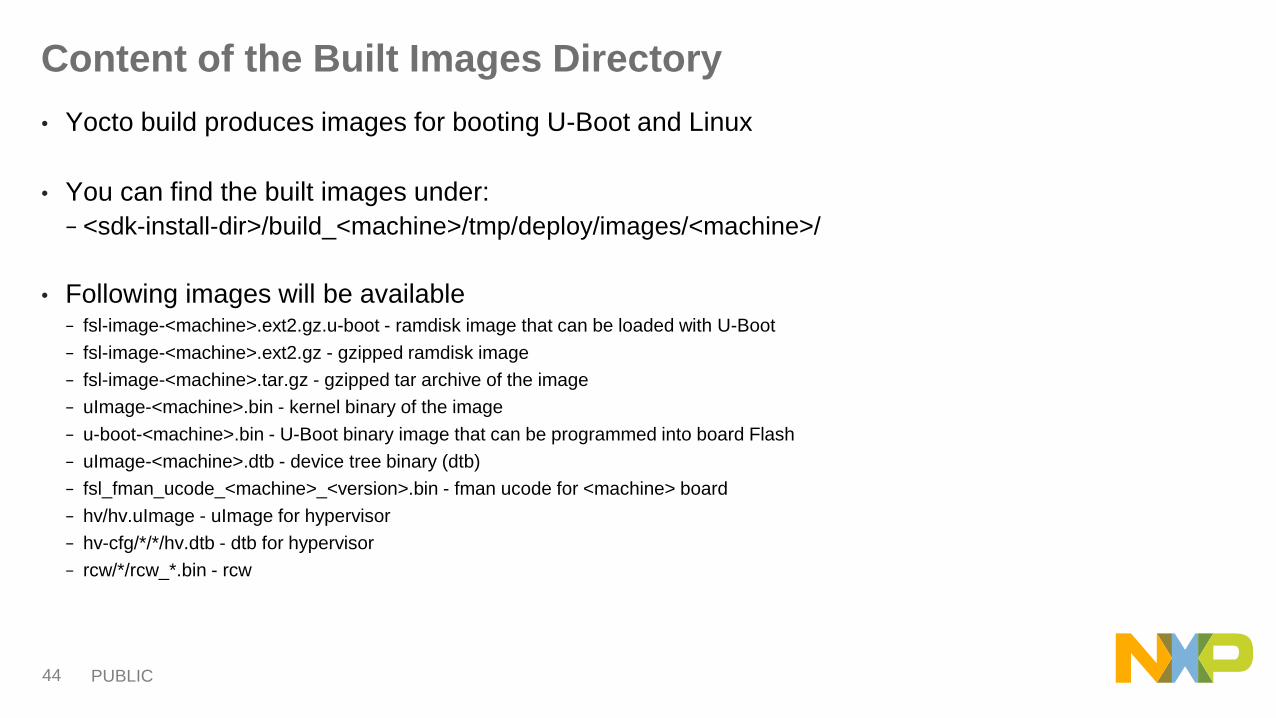
Content of the Built Images Directory
• Yocto build produces images for booting U-Boot and Linux
• You can find the built images under:
− <sdk-install-dir>/build_<machine>/tmp/deploy/images/<machine>/
• Following images will be available− fsl-image-<machine>.ext2.gz.u-boot - ramdisk image that can be loaded with U-Boot
− fsl-image-<machine>.ext2.gz - gzipped ramdisk image
− fsl-image-<machine>.tar.gz - gzipped tar archive of the image
− uImage-<machine>.bin - kernel binary of the image
− u-boot-<machine>.bin - U-Boot binary image that can be programmed into board Flash
− uImage-<machine>.dtb - device tree binary (dtb)
− fsl_fman_ucode_<machine>_<version>.bin - fman ucode for <machine> board
− hv/hv.uImage - uImage for hypervisor
− hv-cfg/*/*/hv.dtb - dtb for hypervisor
− rcw/*/rcw_*.bin - rcw
PUBLIC 45
Building kernel itb FIT image
• LS1043A uses Flattened Image Tree (FIT) format for booting to Linux
• Contains the following:
− Linux Kernel
− Device tree blob
− Root file system
• Build Instructions:
− bitbake -c compile -f fsl-image-kernelitb
− bitbake fsl-image-kernelitb
• New itb can be found in the build directory
− build_<machine>/tmp/deploy/images/<machine>/
PUBLIC 46
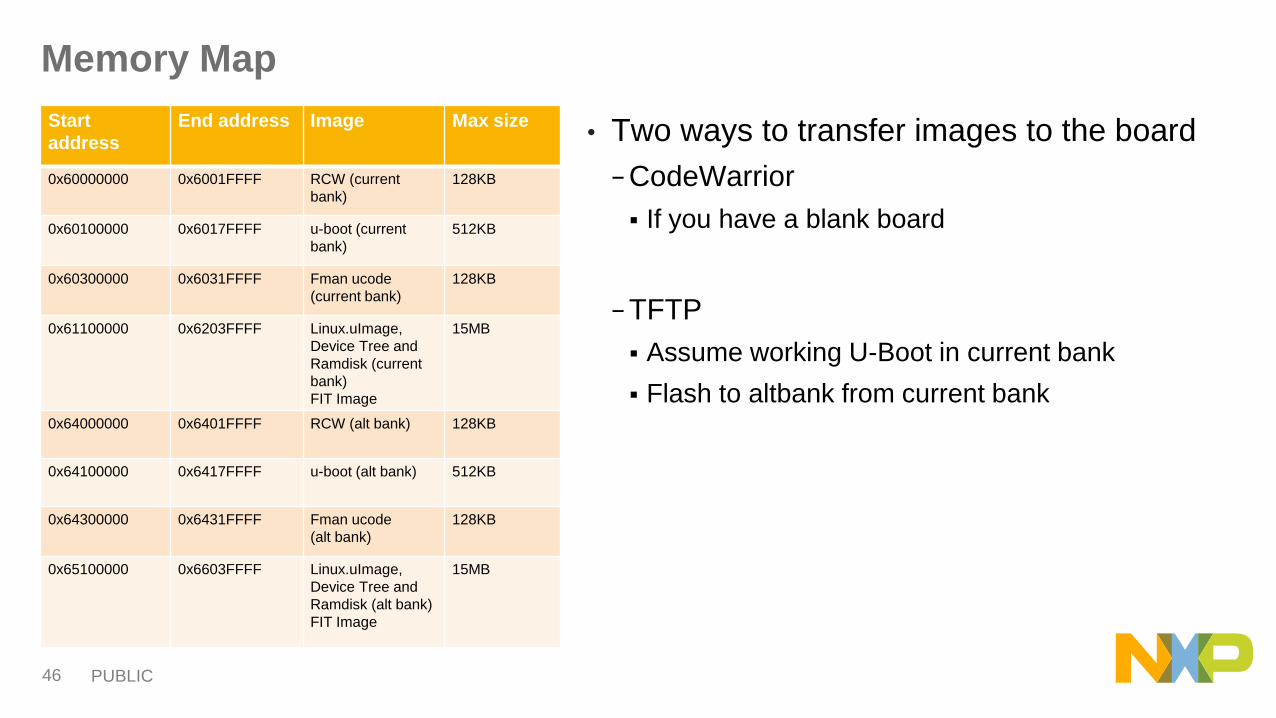
Memory Map
Start
address
End address Image Max size
0x60000000 0x6001FFFF RCW (current
bank)
128KB
0x60100000 0x6017FFFF u-boot (current
bank)
512KB
0x60300000 0x6031FFFF Fman ucode
(current bank)
128KB
0x61100000 0x6203FFFF Linux.uImage,
Device Tree and
Ramdisk (current
bank)
FIT Image
15MB
0x64000000 0x6401FFFF RCW (alt bank) 128KB
0x64100000 0x6417FFFF u-boot (alt bank) 512KB
0x64300000 0x6431FFFF Fman ucode
(alt bank)
128KB
0x65100000 0x6603FFFF Linux.uImage,
Device Tree and
Ramdisk (alt bank)
FIT Image
15MB
• Two ways to transfer images to the board
− CodeWarrior
If you have a blank board
− TFTP
Assume working U-Boot in current bank
Flash to altbank from current bank
PUBLIC 47
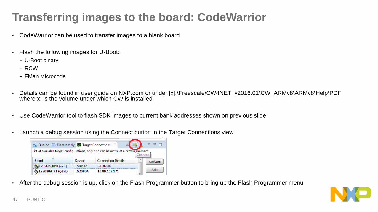
Transferring images to the board: CodeWarrior
• CodeWarrior can be used to transfer images to a blank board
• Flash the following images for U-Boot:
− U-Boot binary
− RCW
− FMan Microcode
• Details can be found in user guide on NXP.com or under [x]:\Freescale\CW4NET_v2016.01\CW_ARMv8\ARMv8\Help\PDFwhere x: is the volume under which CW is installed
• Use CodeWarrior tool to flash SDK images to current bank addresses shown on previous slide
• Launch a debug session using the Connect button in the Target Connections view
• After the debug session is up, click on the Flash Programmer button to bring up the Flash Programmer menu

PUBLIC 48
Transferring images to the board: CodeWarrior
PUBLIC 49
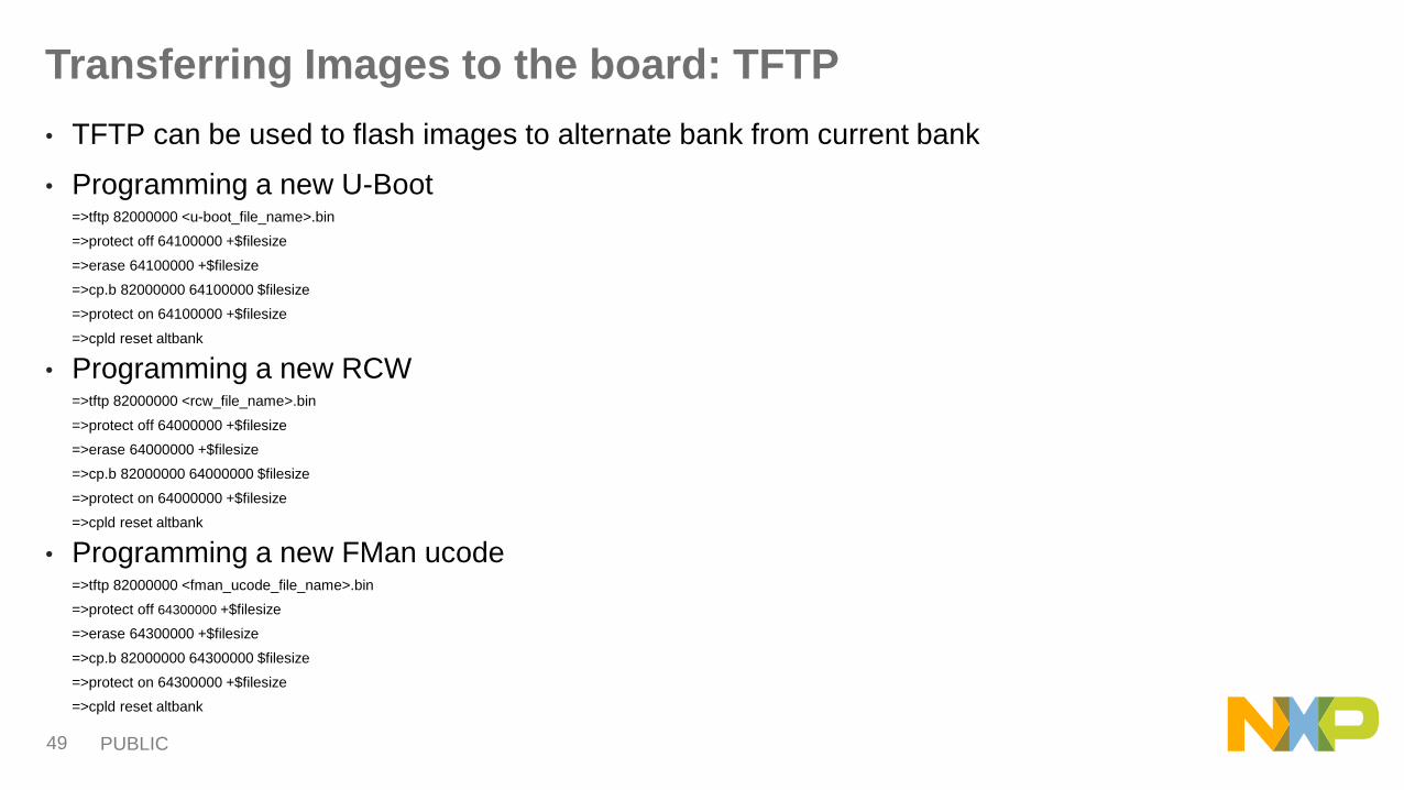
Transferring Images to the board: TFTP
• TFTP can be used to flash images to alternate bank from current bank
• Programming a new U-Boot=>tftp 82000000 <u-boot_file_name>.bin
=>protect off 64100000 +$filesize
=>erase 64100000 +$filesize
=>cp.b 82000000 64100000 $filesize
=>protect on 64100000 +$filesize
=>cpld reset altbank
• Programming a new RCW=>tftp 82000000 <rcw_file_name>.bin
=>protect off 64000000 +$filesize
=>erase 64000000 +$filesize
=>cp.b 82000000 64000000 $filesize
=>protect on 64000000 +$filesize
=>cpld reset altbank
• Programming a new FMan ucode=>tftp 82000000 <fman_ucode_file_name>.bin
=>protect off 64300000 +$filesize
=>erase 64300000 +$filesize
=>cp.b 82000000 64300000 $filesize
=>protect on 64300000 +$filesize
=>cpld reset altbank
PUBLIC 50
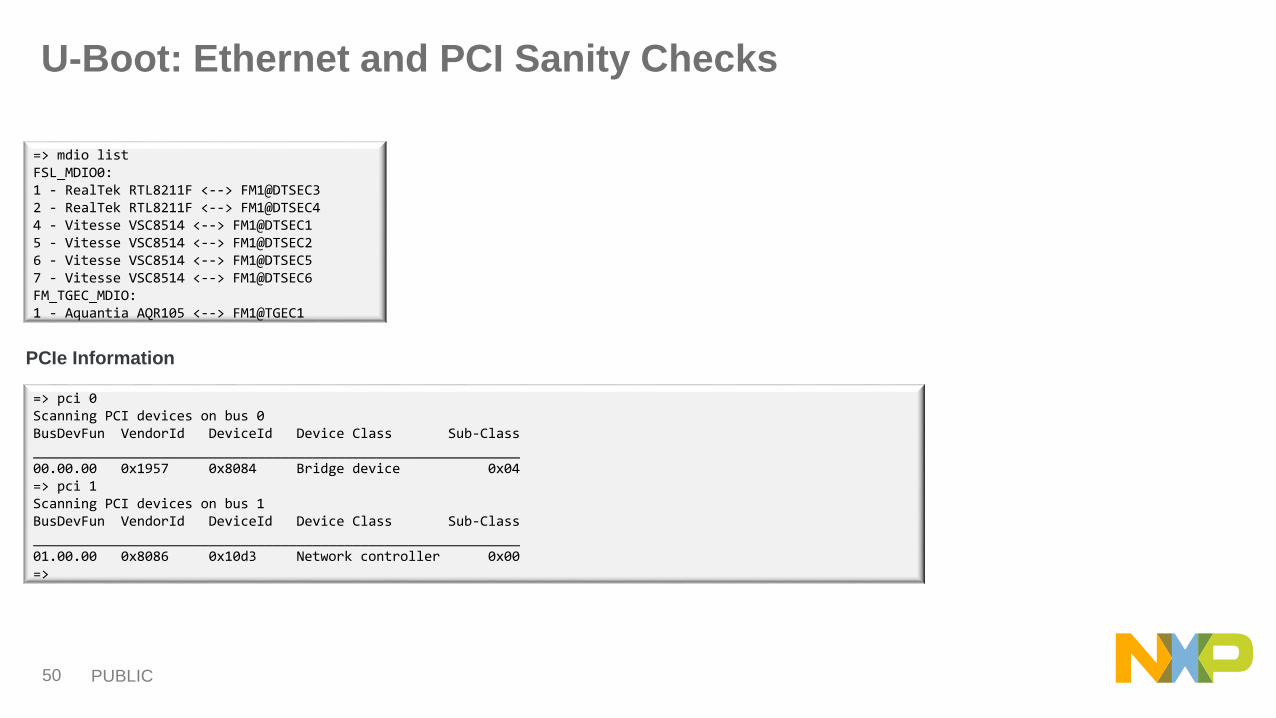
U-Boot: Ethernet and PCI Sanity Checks
=> mdio listFSL_MDIO0:1 - RealTek RTL8211F <--> FM1@DTSEC32 - RealTek RTL8211F <--> FM1@DTSEC44 - Vitesse VSC8514 <--> FM1@DTSEC15 - Vitesse VSC8514 <--> FM1@DTSEC26 - Vitesse VSC8514 <--> FM1@DTSEC57 - Vitesse VSC8514 <--> FM1@DTSEC6FM_TGEC_MDIO:1 - Aquantia AQR105 <--> FM1@TGEC1
PCIe Information
=> pci 0Scanning PCI devices on bus 0BusDevFun VendorId DeviceId Device Class Sub-Class_____________________________________________________________00.00.00 0x1957 0x8084 Bridge device 0x04=> pci 1Scanning PCI devices on bus 1BusDevFun VendorId DeviceId Device Class Sub-Class_____________________________________________________________01.00.00 0x8086 0x10d3 Network controller 0x00=>
PUBLIC 51
FINAL PHASE: POST
BOOT & BEYOND
Suggested sessions: FTF-DES-N1853
PUBLIC 52
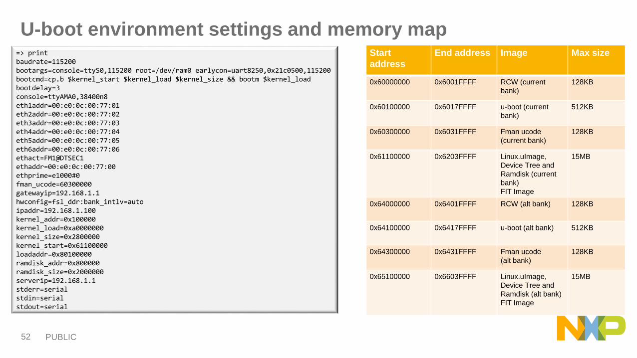
U-boot environment settings and memory map=> printbaudrate=115200bootargs=console=ttyS0,115200 root=/dev/ram0 earlycon=uart8250,0x21c0500,115200bootcmd=cp.b $kernel_start $kernel_load $kernel_size && bootm $kernel_loadbootdelay=3console=ttyAMA0,38400n8eth1addr=00:e0:0c:00:77:01eth2addr=00:e0:0c:00:77:02eth3addr=00:e0:0c:00:77:03eth4addr=00:e0:0c:00:77:04eth5addr=00:e0:0c:00:77:05eth6addr=00:e0:0c:00:77:06ethact=FM1@DTSEC1ethaddr=00:e0:0c:00:77:00ethprime=e1000#0fman_ucode=60300000gatewayip=192.168.1.1hwconfig=fsl_ddr:bank_intlv=autoipaddr=192.168.1.100kernel_addr=0x100000kernel_load=0xa0000000kernel_size=0x2800000kernel_start=0x61100000loadaddr=0x80100000ramdisk_addr=0x800000ramdisk_size=0x2000000serverip=192.168.1.1stderr=serialstdin=serialstdout=serial
Start
address
End address Image Max size
0x60000000 0x6001FFFF RCW (current
bank)
128KB
0x60100000 0x6017FFFF u-boot (current
bank)
512KB
0x60300000 0x6031FFFF Fman ucode
(current bank)
128KB
0x61100000 0x6203FFFF Linux.uImage,
Device Tree and
Ramdisk (current
bank)
FIT Image
15MB
0x64000000 0x6401FFFF RCW (alt bank) 128KB
0x64100000 0x6417FFFF u-boot (alt bank) 512KB
0x64300000 0x6431FFFF Fman ucode
(alt bank)
128KB
0x65100000 0x6603FFFF Linux.uImage,
Device Tree and
Ramdisk (alt bank)
FIT Image
15MB
PUBLIC 53
Linux Images
• Options for loading Linux images onto board
− Use TFTP from PC
− Use Serial Port from PC
PUBLIC 54
Using TFTP to Load Linux Images and Boot
• Set up TFTP server on your PC
• Make sure IP Address of PC is same as serverip set previously
• Ping serverip to make sure a live link is available− =>ping $serverip
• TFTP itb image and flash it to the NOR flash vBank0 using following commands− =>tftp a0000000 kernel-ls1043ardb.itb
− =>erase 61100000 +$filesize
− =>cp.b a0000000 61100000 $filesize
• Use command: “boot” to bring up linux
PUBLIC 55
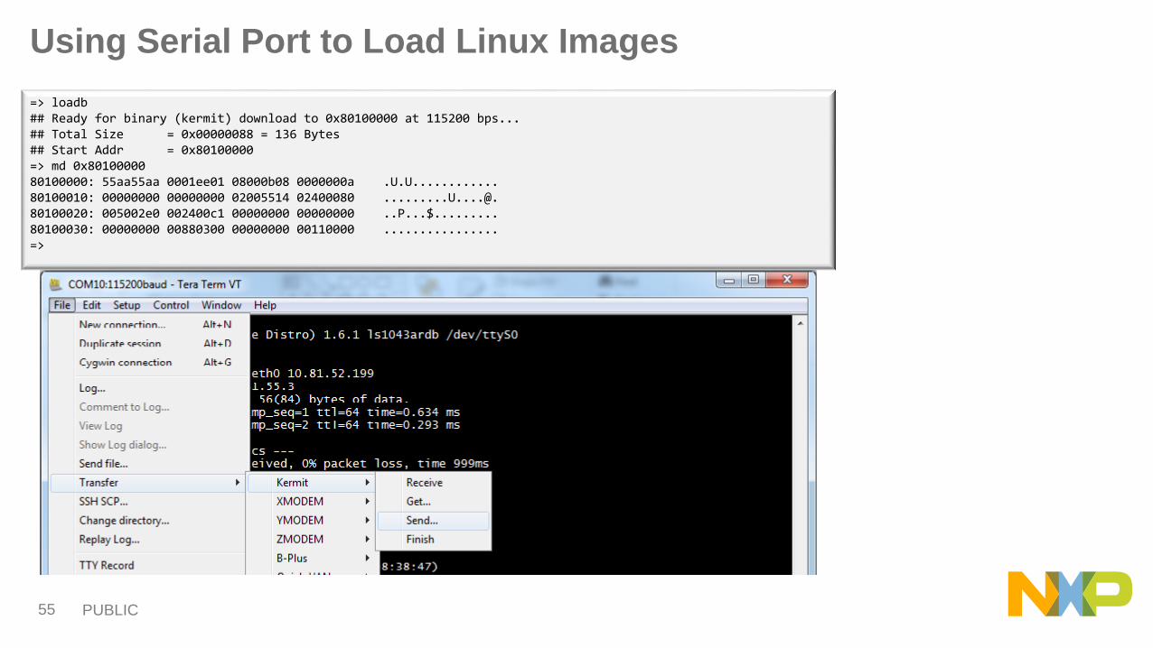
=> loadb## Ready for binary (kermit) download to 0x80100000 at 115200 bps...## Total Size = 0x00000088 = 136 Bytes## Start Addr = 0x80100000=> md 0x8010000080100000: 55aa55aa 0001ee01 08000b08 0000000a .U.U............80100010: 00000000 00000000 02005514 02400080 [email protected]: 005002e0 002400c1 00000000 00000000 ..P...$.........80100030: 00000000 00880300 00000000 00110000 ................=>
Using Serial Port to Load Linux Images


