
TSL2771
LIGHT-TO-DIGITAL CONVERTER
with PROXIMITY SENSINGTAOS100B − FEBRUARY 2011
1
The LUMENOLOGY � Company�
�
Copyright � 2011, TAOS Inc.
www.taosinc.com
Features
� Ambient Light Sensing and ProximityDetection in a Single Device
� Ambient Light Sensing (ALS)− Approximates Human Eye Response− Programmable Analog Gain− Programmable Integration Time− Programmable Interrupt Function with
Upper and Lower Threshold− Resolution Up to 16 Bits− Very High Sensitivity — Operates Well
Behind Darkened Glass− Up to 1,000,000:1 Dynamic Range
� Proximity Detection− Programmable Number of IR Pulses− Programmable Current Sink for the IR
LED — No Limiting Resistor Needed− Programmable Interrupt Function with
Upper and Lower Threshold− Covers a 2000:1 Dynamic Range
� Programmable Wait Timer− Programmable from 2.72 ms
to > 8 Seconds− Wait State — 65 �A Typical Current
� I2C Interface Compatible− Up to 400 kHz (I2C Fast Mode)− Dedicated Interrupt Pin
� Small 2 mm � 2 mm ODFN Package
� Sleep Mode — 2.5 �A Typical Current
Applications� Cell Phone Backlight Dimming
� Cell Phone Touch Screen Disable
� Notebook/Monitor Security
� Automatic Speakerphone Enable
� Automatic Menu Popup
Description
The TSL2771 family of devices provides both ambient light sensing (ALS) and proximity detection (whencoupled with an external IR LED). The ALS approximates human eye response to light intensity under a varietyof lighting conditions and through a variety of attenuation materials. The proximity detection feature allows alarge dynamic range of operation for use in short distance detection behind dark glass such as in a cell phoneor for longer distance measurements for applications such as presence detection for monitors or laptops. Theprogrammable proximity detection enables continuous measurements across the entire range. In addition, aninternal state machine provides the ability to put the device into a low power mode in between ALS and proximitymeasurements providing very low average power consumption.
While useful for general purpose light sensing, the device is particularly useful for display management with thepurpose of extending battery life and providing optimum viewing in diverse lighting conditions. Display paneland keyboard backlighting can account for up to 30 to 40 percent of total platform power. The ALS features areideal for use in tablets, notebook PCs, LCD monitors, flat-panel televisions, and cell phones.
The proximity function is targeted specifically towards cell phone, LCD monitor, laptop, and flat-panel televisionapplications. In cell phones, the proximity detection can detect when the user positions the phone close to theirear. The device is fast enough to provide proximity information at a high repetition rate needed when answeringa phone call. It can also detect both close and far distances so the application can implement more complexalgorithms to provide a more robust interface. In laptop or monitor applications, the product is sensitive enoughto determine whether a user is in front of the laptop using the keyboard or away from the desk. This providesboth improved green power saving capability and the added security to lock the computer when the user is notpresent.
�
�
Texas Advanced Optoelectronic Solutions Inc.1001 Klein Road � Suite 300 � Plano, TX 75074 � (972) 673-0759
PACKAGE FNDUAL FLAT NO-LEAD
(TOP VIEW)
VDD 1
SCL 2
GND 3
6 SDA
5 INT
4 LDR
Package Image Not Actual Size

TSL2771
LIGHT-TO-DIGITAL CONVERTER
with PROXIMITY SENSINGTAOS100B − FEBRUARY 2011
2
�
�
Copyright � 2011, TAOS Inc. The LUMENOLOGY � Company
www.taosinc.com
Functional Block Diagram
CH0
SDA
VDD
INT
SCL
LDR
CH1ADC
ALS Control
CH1Data
Wait Control
ProxADC
Prox Control
ProxData
IR LED ConstantCurrent Sink
CH0ADC
CH0Data
ProxIntegration
CH1
Upper Limit
Upper Limit
Lower Limit
Lower Limit
Interrupt
I2C
Inte
rfac
e
GND
Detailed Description
The TSL2771 light-to-digital device provides on-chip photodiodes, integrating amplifiers, ADCs, accumulators,clocks, buffers, comparators, a state machine, and an I2C interface. Each device combines a Channel 0photodiode (CH0), which is responsive to both visible and infrared light, and a channel 1 photodiode (CH1),which is responsive primarily to infrared light. Two integrating ADCs simultaneously convert the amplifiedphotodiode currents into a digital value providing up to 16 bits of resolution. Upon completion of the conversioncycle, the conversion result is transferred to the data registers. This digital output can be read by amicroprocessor through which the illuminance (ambient light level) in Lux is derived using an empirical formulato approximate the human eye response.
Communication to the device is accomplished through a fast (up to 400 kHz), two-wire I2C serial bus for easyconnection to a microcontroller or embedded controller. The digital output of the device is inherently moreimmune to noise when compared to an analog interface.
The device provides a separate pin for level-style interrupts. When interrupts are enabled and a pre-set valueis exceeded, the interrupt pin is asserted and remains asserted until cleared by the controlling firmware. Theinterrupt feature simplifies and improves system efficiency by eliminating the need to poll a sensor for a lightintensity or proximity value. An interrupt is generated when the value of an ALS or proximity conversion exceedseither an upper or lower threshold. In addition, a programmable interrupt persistence feature allows the userto determine how many consecutive exceeded thresholds are necessary to trigger an interrupt. Interruptthresholds and persistence settings are configured independently for both ALS and proximity.
Proximity detection requires only a single external IR LED. An internal LED driver can be configured to providea constant current sink of 12.5 mA, 25 mA, 50 mA, or 100 mA of current. No external current limiting resistoris required. The number of proximity LED pulses can be programmed from 1 to 255 pulses. Each pulse has a16-μs period. This LED current, coupled with the programmable number of pulses, provides a 2000:1contiguous dynamic range.

TSL2771
LIGHT-TO-DIGITAL CONVERTER
with PROXIMITY SENSINGTAOS100B − FEBRUARY 2011
3
The LUMENOLOGY � Company�
�
Copyright � 2011, TAOS Inc.
www.taosinc.com
Terminal Functions
TERMINALTYPE DESCRIPTION
NAME NO.TYPE DESCRIPTION
GND 3 Power supply ground. All voltages are referenced to GND.
INT 5 O Interrupt — open drain (active low).
LDR 4 O LED driver for proximity emitter — up to 100 mA, open drain.
SCL 2 I I2C serial clock input terminal — clock signal for I2C serial data.
SDA 6 I/O I2C serial data I/O terminal — serial data I/O for I2C .
VDD 1 Supply voltage.
Available Options
DEVICE ADDRESS PACKAGE − LEADS INTERFACE DESCRIPTION ORDERING NUMBER
TSL27711 0x39 FN−6 I2C Vbus = VDD Interface TSL27711FN
TSL27713 0x39 FN−6 I2C Vbus = 1.8 V Interface TSL27713FN
TSL27715† 0x29 FN−6 I2C Vbus = VDD Interface TSL27715FN
TSL27717† 0x29 FN−6 I2C Vbus = 1.8 V Interface TSL27717FN† Contact TAOS for availability.
Absolute Maximum Ratings over operating free-air temperature range (unless otherwise noted)†
Supply voltage, VDD (see Note 1) 3.8 V. . . . . . . . . . . . . . . . . . . . . . . . . . . . . . . . . . . . . . . . . . . . . . . . . . . . . . . . . . . Digital output voltage range, VO −0.5 V to 3.8 V. . . . . . . . . . . . . . . . . . . . . . . . . . . . . . . . . . . . . . . . . . . . . . . . . . . . Digital output current, IO −1 mA to 20 mA. . . . . . . . . . . . . . . . . . . . . . . . . . . . . . . . . . . . . . . . . . . . . . . . . . . . . . . . . . Storage temperature range, Tstg −40°C to 85°C. . . . . . . . . . . . . . . . . . . . . . . . . . . . . . . . . . . . . . . . . . . . . . . . . . . . ESD tolerance, human body model 2000 V. . . . . . . . . . . . . . . . . . . . . . . . . . . . . . . . . . . . . . . . . . . . . . . . . . . . . . . .
† Stresses beyond those listed under “absolute maximum ratings” may cause permanent damage to the device. These are stress ratings only, andfunctional operation of the device at these or any other conditions beyond those indicated under “recommended operating conditions” is notimplied. Exposure to absolute-maximum-rated conditions for extended periods may affect device reliability.
NOTE 1: All voltages are with respect to GND.
Recommended Operating Conditions
MIN NOM MAX UNIT
Supply voltage, VDD 2.6 3 3.6 V
Operating free-air temperature, TA −30 70 °C

TSL2771
LIGHT-TO-DIGITAL CONVERTER
with PROXIMITY SENSINGTAOS100B − FEBRUARY 2011
4
�
�
Copyright � 2011, TAOS Inc. The LUMENOLOGY � Company
www.taosinc.com
Operating Characteristics, VDD = 3 V, TA = 25�C (unless otherwise noted)
PARAMETER TEST CONDITIONS MIN TYP MAX UNIT
Active — LDR pulses off 175 250
IDD Supply current Wait mode 65 μAIDD Supply current
Sleep mode — no I2C activity 2.5 4
μA
V INT SDA output low voltage3 mA sink current 0 0.4
VVOL INT, SDA output low voltage6 mA sink current 0 0.6
V
I LEAK Leakage current, SDA, SCL, INT pins −5 5 μA
I LEAK Leakage current, LDR pin ± 10 μA
V SCL SDA input high voltageTSL27711, TSL27715 0.7 VDD
VVIH SCL, SDA input high voltageTSL27713, TSL27717 1.25
V
V SCL SDA input low voltageTSL27711, TSL27715 0.3 VDD
VVIL SCL, SDA input low voltageTSL27713, TSL27717 0.54
V
ALS Characteristics, VDD = 3 V, TA = 25�C, Gain = 16, AEN = 1 (unless otherwise noted) (Notes 1 ,2, 3)
PARAMETER TEST CONDITIONS CHANNEL MIN TYP MAX UNIT
Dark ADC count valueEe = 0, AGAIN = 120×, CH0 0 1 5
countsDark ADC count valueEe = 0, AGAIN = 120×,ATIME = 0xDB (100 ms) CH1 0 1 5
counts
ADC integration time step size ATIME = 0xFF 2.58 2.72 2.9 ms
ADC Number of integration steps 1 256 steps
ADC counts per step ATIME = 0xFF 0 1024 counts
ADC count value ATIME = 0xC0 0 65535 counts
λp = 625 nm, Ee = 171.6 μW/cm2, CH0 4000 5000 6000
ADC count value
λp = 625 nm, Ee = 171.6 μW/cm , ATIME = 0xF6 (27 ms) See note 2. CH1 790
countsADC count valueλp = 850 nm, Ee = 219.7 μW/cm2, CH0 4000 5000 6000
countsλp = 850 nm, Ee = 219.7 μW/cm , ATIME = 0xF6 (27 ms) See note 3. CH1 2800
λ 625 nm ATIME 0xF6 (27 ms) See note 2 10 8 15 8 20 8ADC count value ratio: CH1/CH0
λp = 625 nm, ATIME = 0xF6 (27 ms) See note 2. 10.8 15.8 20.8%ADC count value ratio: CH1/CH0
λ 850 nm ATIME 0xF6 (27 ms) See note 3 41 56 68%ADC count value ratio: CH1/CH0
λp = 850 nm, ATIME = 0xF6 (27 ms) See note 3. 41 56 68%
λp = 625 nm, ATIME = 0xF6 (27 ms) CH0 29.1
R Irradiance responsivity
λp = 625 nm, ATIME = 0xF6 (27 ms)See note 2. CH1 4.6 counts/
(μW/Re Irradiance responsivityλp = 850 nm, ATIME = 0xF6 (27 ms) CH0 22.8
(μW/cm2)λp = 850 nm, ATIME = 0xF6 (27 ms)
See note 3. CH1 12.7cm2)
G i li l ti t 1× i8× −10 10
Gain scaling, relative to 1× gain16× 10 10 %
Gain scaling, relative to 1× gainsetting 16× −10 10 %setting
120× −10 10
%
NOTES: 1. Optical measurements are made using small-angle incident radiation from light-emitting diode optical sources. Visible 625 nm LEDsand infrared 850 nm LEDs are used for final product testing for compatibility with high-volume production.
2. The 625 nm irradiance Ee is supplied by an AlInGaP light-emitting diode with the following typical characteristics: peak wavelengthλp = 625 nm and spectral halfwidth Δλ½ = 20 nm.
3. The 850 nm irradiance Ee is supplied by a GaAs light-emitting diode with the following typical characteristics: peak wavelength λp = 850 nm and spectral halfwidth Δλ½ = 42 nm.

TSL2771
LIGHT-TO-DIGITAL CONVERTER
with PROXIMITY SENSINGTAOS100B − FEBRUARY 2011
5
The LUMENOLOGY � Company�
�
Copyright � 2011, TAOS Inc.
www.taosinc.com
Proximity Characteristics, VDD = 3 V, TA = 25�C, PEN = 1 (unless otherwise noted)
PARAMETER TEST CONDITIONS CONDITION MIN TYP MAX UNIT
IDD Supply current LDR pulse on 3 mA
ADC conversion time step size PTIME = 0xFF 2.58 2.72 2.9 ms
ADC number of integration steps 1 256 steps
ADC counts per step PTIME = 0xFF 0 1023 counts
IR LED pulse count 0 255 pulses
pulse period Two or more pulses 16 μs
LED pulse width — LED on time 7.3 μs
PDRIVE=0 75 100 125
LED drive currentISINK sink current @ 600 mV, PDRIVE=1 50
mALED drive currentISINK sink current @ 600 mV, LDR pin PDRIVE=2 25
mA
PDRIVE=3 12.5
Operating distance (See note 1) 18 inches
NOTE 1: Proximity Operating Distance is dependent upon emitter properties and the reflective properties of the proximity surface. The nominalvalue shown uses an IR emitter with a peak wavelength of 850nm and a 20° half angle. The proximity surface used is a 90% reflective(white surface) 16 × 20-inch Kodak Gray Card. 60 mw/SR, 100 mA, 64 pulses, open view (no glass). Note: Greater distances areachievable with appropriate system considerations.
Wait Characteristics, VDD = 3 V, TA = 25�C, WEN = 1 (unless otherwise noted)
PARAMETER TEST CONDITIONS CHANNEL MIN TYP MAX UNIT
Wait step size WTIME = 0xFF 2.58 2.72 2.9 ms
Wait number of integration steps 1 256 steps
AC Electrical Characteristics, VDD = 3 V, TA = 25�C (unless otherwise noted)
PARAMETER† TEST CONDITIONS MIN TYP MAX UNIT
f(SCL) Clock frequency (I2C only) 0 400 kHz
t(BUF) Bus free time between start and stop condition 1.3 μs
t(HDSTA)Hold time after (repeated) start condition. Afterthis period, the first clock is generated.
0.6 μs
t(SUSTA) Repeated start condition setup time 0.6 μs
t(SUSTO) Stop condition setup time 0.6 μs
t(HDDAT) Data hold time 0 μs
t(SUDAT) Data setup time 100 ns
t(LOW) SCL clock low period 1.3 μs
t(HIGH) SCL clock high period 0.6 μs
tF Clock/data fall time 300 ns
tR Clock/data rise time 300 ns
Ci Input pin capacitance 10 pF† Specified by design and characterization; not production tested.

TSL2771
LIGHT-TO-DIGITAL CONVERTER
with PROXIMITY SENSINGTAOS100B − FEBRUARY 2011
6
�
�
Copyright � 2011, TAOS Inc. The LUMENOLOGY � Company
www.taosinc.com
PARAMETER MEASUREMENT INFORMATION
SDA
SCL
StopStart
SCLACKt(LOWMEXT) t(LOWMEXT)
t(LOWSEXT)
SCLACK
t(LOWMEXT)
StartCondition
StopCondition
P
SDA
t(SUSTO)t(SUDAT)t(HDDAT)t(BUF)
VIH
VIL
SCL
t(SUSTA)t(HIGH)
t(F)t(R)
t(HDSTA)
t(LOW)
VIH
VIL
P SS
Figure 1. Timing Diagrams

TSL2771
LIGHT-TO-DIGITAL CONVERTER
with PROXIMITY SENSINGTAOS100B − FEBRUARY 2011
7
The LUMENOLOGY � Company�
�
Copyright � 2011, TAOS Inc.
www.taosinc.com
TYPICAL CHARACTERISTICS
Figure 2
SPECTRAL RESPONSIVITY
λ − Wavelength − nm
0400
0.2
0.4
0.6
0.8
1
500 600 700 800 900 1000 1100
No
rmal
ized
Res
po
nsi
vity
300
Ch 0
Ch 1
25 mA
12.5 mA
Figure 3
LDR Voltage − V
LD
R C
urr
ent
— m
A
TYPICAL LDR CURRENTvs.
VOLTAGE
50 mA
100 mA
0 0.5 1 1.5 2 2.50
20
40
60
80
100
120
140
160
3
Figure 4
NORMALIZED IDDvs.
VDD and TEMPERATURE
VDD — V
I DD
No
rmal
ized
@ 3
V, 2
5�C
94%
96%
98%
100%
102%
104%
106%
108%
110%
92%2.7 2.8 2.9 3 3.1 3.2 3.3
75�C
50�C 25�C
0�C
Figure 5
NORMALIZED RESPONSIVITYvs.
ANGULAR DISPLACEMENT
� − Angular Displacement − °
No
rmal
ized
Res
po
nsi
vity
0
0.2
0.4
0.6
0.8
1.0
−90 −60 −30 0 30 60 90
Op
tica
l Axi
s
�� ��

TSL2771
LIGHT-TO-DIGITAL CONVERTER
with PROXIMITY SENSINGTAOS100B − FEBRUARY 2011
8
�
�
Copyright � 2011, TAOS Inc. The LUMENOLOGY � Company
www.taosinc.com
PRINCIPLES OF OPERATION
System State Machine
The device provides control of ALS, proximity detection, and power management functionality through aninternal state machine (Figure 6). After a power-on-reset, the device is in the sleep mode. As soon as the PONbit is set, the device will move to the start state. It will then continue through the Prox, Wait, and ALS states. Ifthese states are enabled, the device will execute each function. If the PON bit is set to 0, the state machine willcontinue until all conversions are completed and then go into a low power sleep mode.
Sleep
Start
Wait
ALSProx
PON = 1 (r0:b0) PON = 0 (r0:b0)
Figure 6. Simplified State Diagram
NOTE: In this document, the nomenclature uses the bit field name in italics followed by the register number andbit number to allow the user to easily identify the register and bit that controls the function. For example, thepower on (PON) is in register 0, bit 0. This is represented as PON (r0:b0).
Photodiodes
Conventional silicon detectors respond strongly to infrared light, which the human eye does not see. This canlead to significant error when the infrared content of the ambient light is high (such as with incandescent lighting)due to the difference between the silicon detector response and the brightness perceived by the human eye.
This problem is overcome through the use of two photodiodes. The Channel 0 photodiode, referred to as theCH0 channel, is sensitive to both visible and infrared light, while the Channel 1 photodiode, referred to as CH1,is sensitive primarily to infrared light. Two integrating ADCs convert the photodiode currents to digital outputs.The ADC digital outputs from the two channels are used in a formula to obtain a value that approximates thehuman eye response in units of lux.

TSL2771
LIGHT-TO-DIGITAL CONVERTER
with PROXIMITY SENSINGTAOS100B − FEBRUARY 2011
9
The LUMENOLOGY � Company�
�
Copyright � 2011, TAOS Inc.
www.taosinc.com
ALS Operation
The ALS engine contains ALS gain control (AGAIN) and two integrating analog-to-digital converters (ADC) forthe Channel 0 and Channel 1 photodiodes. The ALS integration time (ATIME) impacts both the resolution andthe sensitivity of the ALS reading. Integration of both channels occurs simultaneously and upon completion ofthe conversion cycle, the results are transferred to the data registers (C0DATA and C1DATA). This data is alsoreferred to as channel count. The transfers are double-buffered to ensure data integrity.
CH1ADC
ALS Control
CH1Data
CH0ALS
CH0Data
AGAIN(r0x0F, b1:0)1�, 8�, 16�, 120� Gain
CH0
CH1
C0DATAH(r0x15), C0DATA(r0x14)
C1DATAH(r0x17), C1DATA(r0x16)
ATIME(r 1)2.72 ms to 696 ms
Figure 7. ALS Operation
The registers for programming the integration and wait times are a 2’s compliment values. The actual time canbe calculated as follows:
ATIME = 256 − Integration Time / 2.72 ms
Inversely, the time can be calculated from the register value as follows:Integration Time = 2.72 ms × (256 − ATIME)
In order to reject 50/60-Hz ripple strongly present in fluorescent lighting, the integration time needs tobe programmed in multiples of 10 / 8.3 ms or the half cycle time. Both frequencies can be rejected with aprogrammed value of 50 ms (ATIME = 0xED) or multiples of 50 ms (i.e. 100, 150, 200, 400, 600).
The registers for programming the AGAIN hold a two-bit value representing a gain of 1×, 8×, 16×, or 120×. Thegain, in terms of amount of gain, will be represented by the value AGAINx, i.e. AGAINx = 1, 8, 16, or 120.
Lux Equation
The lux calculation is a function of CH0 channel count (C0DATA), CH1 channel count (C1DATA), ALS gain(AGAINx), and ALS integration time in milliseconds (ATIME_ms). If an aperture, glass/plastic, or a light pipeattenuates the light equally across the spectrum (300 nm to 1100 nm), then a scaling factor referred to as glassattenuation (GA) can be used to compensate for attenuation. For a device in open air with no aperture orglass/plastic above the device, GA = 1. If it is not spectrally flat, then a custom lux equation with new coefficientsshould be generated. (See TAOS application note).
Counts per Lux (CPL) needs to be calculated only when ATIME or AGAIN is changed, otherwise it remains aconstant. The first segment of the equation (Lux1) covers fluorescent and incandescent light. The secondsegment (Lux2) covers dimmed incandescent light. The final lux is the maximum of Lux1, Lux2, or 0.
CPL = (ATIME_ms × AGAINx) / (GA × 53) Lux1 = (C0DATA − 2 × C1DATA) / CPLLux2 = (0.6 × C0DATA − C1DATA) / CPLLux = MAX(Lux1, Lux2, 0)

TSL2771
LIGHT-TO-DIGITAL CONVERTER
with PROXIMITY SENSINGTAOS100B − FEBRUARY 2011
10
�
�
Copyright � 2011, TAOS Inc. The LUMENOLOGY � Company
www.taosinc.com
Proximity Detection
Proximity sensing uses an external light source (generally an infrared emitter) to emit light, which is then viewedby the integrated light detector to measure the amount of reflected light when an object is in the light path(Figure 8). The amount of light detected from a reflected surface can then be used to determine an object’sproximity to the sensor.
IR LED
ProxSensor
Surface Reflectivity (SR)
Background Energy (BGE) Optical Crosstalk (OC)
Glass Attenuation (GA)
Distance (D)
Figure 8. Proximity Detection
The device has controls for the number of IR pulses (PPCOUNT), the integration time (PTIME), the LED drivecurrent (PDRIVE), and the photodiode configuration (PDIODE) (Figure 9). The photodiode configuration canbe set to CH1 diode (recommended), CH0 diode, or a combination of both diodes. At the end of the integrationcycle, the results are latched into the proximity data (PDATA) register.
CH1
ProxIntegration
Prox Control
ProxADC
IR LED ConstantCurrent Sink
CH0
PDATAH(r0x019), PDATAL(r0x018)
PDRIVE(r 0x0F, b7:6)
ProxData
IRLED
PTIME(r 2)
PPCOUNT(r0x0E)
VDD
Figure 9. Proximity Detection Operation
The LED drive current is controlled by a regulated current sink on the LDR pin. This feature eliminates the needto use a current limiting resistor to control LED current. The LED drive current can be configured for 12.5 mA,25 mA, 50 mA, or 100 mA. For higher LED drive requirements, an external P type transistor can be used tocontrol the LED current.

TSL2771
LIGHT-TO-DIGITAL CONVERTER
with PROXIMITY SENSINGTAOS100B − FEBRUARY 2011
11
The LUMENOLOGY � Company�
�
Copyright � 2011, TAOS Inc.
www.taosinc.com
The number of LED pulses can be programmed to any value between 1 and 255 pulses as needed. Increasingthe number of LED pulses at a given current will increase the sensor sensitivity. Sensitivity grows by the squareroot of the number of pulses. Each pulse has a 16-μs period.
LED On LED Off
16 �s
IR LED Pulses
SubtractBackground
Add IR +Background
Figure 10. Proximity IR LED Waveform
The proximity integration time (PTIME) is the period of time that the internal ADC converts the analog signalto a digital count. It is recommend that this be set to a minimum of PTIME = 0xFF or 2.72 ms.
The combination of LED power and number of pulses can be used to control the distance at which the sensorcan detect proximity. Figure 11 shows an example of the distances covered with settings such that each curvecovers 2× the distance. Counts up to 64 pulses provide a 16× range.
Figure 11
PROXIMITY ADC COUNTvs.
RELATIVE DISTANCE
Pro
xim
ity
AD
C C
ou
nt
Relative Distance
1� 2� 4� 8� 16�
0
200
400
600
800
1000
100 mA,64 Pulses
100 mA,16 Pulses
100 mA,4 Pulses
100 mA,1 Pulse
25 mA,1 Pulse

TSL2771
LIGHT-TO-DIGITAL CONVERTER
with PROXIMITY SENSINGTAOS100B − FEBRUARY 2011
12
�
�
Copyright � 2011, TAOS Inc. The LUMENOLOGY � Company
www.taosinc.com
Interrupts
The interrupt feature simplifies and improves system efficiency by eliminating the need to poll the sensor forlight intensity or proximity values outside of a user-defined range. While the interrupt function is always enabledand it’s status is available in the status register (0x13), the output of the interrupt state can be enabled usingthe proximity interrupt enable (PIEN) or ALS interrupt enable (AIEN) fields in the enable register (0x00).
Four 16-bit interrupt threshold registers allow the user to set limits below and above a desired light level andproximity range. An interrupt can be generated when the ALS CH0 data (C0DATA) falls outside of the desiredlight level range, as determined by the values in the ALS interrupt low threshold registers (AILTx) and ALSinterrupt high threshold registers (AIHTx). Likewise, an out-of-range proximity interrupt can be generated whenthe proximity data (PDATA) falls below the proximity interrupt low threshold (PILTx) or exceeds the proximityinterrupt high threshold (PIHTx). It is important to note that the low threshold value must be less than the highthreshold value for proper operation.
To further control when an interrupt occurs, the device provides a persistence filter. The persistence filter allowsthe user to specify the number of consecutive out-of-range ALS or proximity occurrences before an interruptis generated. The persistence register (0x0C) allows the user to set the ALS persistence (APERS) and theproximity persistence (PPERS) values. See the persistence register for details on the persistence filter values.Once the persistence filter generates an interrupt, it will continue until a special function interrupt clear commandis received (see command register).
ProxADC
ProxData
CH0ADC
CH0Data
ProxIntegration
CH0
CH1
Upper Limit
Upper Limit
Lower Limit
Lower Limit
Prox Persistence
PILTH(r09), PILTL(r08)
AIHTH(r07), AIHTL(r06)
ALS Persistence
AILTH(r05), AILTL(r04)
PIHTH(r0x0B), PIHTL(r0x0A) PPERS(r 0x0C, b7:4)
APERS(r0x0C, b3:0)
Figure 12. Programmable Interrupt

TSL2771
LIGHT-TO-DIGITAL CONVERTER
with PROXIMITY SENSINGTAOS100B − FEBRUARY 2011
13
The LUMENOLOGY � Company�
�
Copyright � 2011, TAOS Inc.
www.taosinc.com
State Diagram
Figure 13 shows a more detailed flow for the state machine. The device starts in the sleep mode. The PON bitis written to enable the device. A 2.72-ms delay will occur before entering the start state. If the PEN bit is set,the state machine will step through the proximity states of proximity accumulate and then proximity ADCconversion. As soon as the conversion is complete, the state machine will move to the following state.
If the WEN bit is set, the state machine will then cycle through the wait state. If the WLONG bit is set, the waitcycles are extended by 12× over normal operation. When the wait counter terminates, the state machine willstep to the ALS state.
The AEN should always be set, even in proximity-only operation. In this case, a minimum of 1 integration timestep should be programmed. The ALS state machine will continue until it reaches the terminal count at whichpoint the data will be latched in the ALS register and the interrupt set, if enabled.
ProxCheck
PON = 1 PON = 0
Sleep
ALSCheck
WaitCheck
Start
Wait
WEN = 1
ProxAccum
ProxADC
ALS
ALSDelay
PEN = 1
AEN = 1
Up to 255 LED PulsesPulse Frequency: 62.5 kHzTime: 16 �s − 4.2 msMaximum 4.2ms
Up to 256 stepsStep: 2.72 ms
Time: 2.72 ms − 696 ms120 Hz Minimum − 8 ms
100 Hz Minimum − 10 ms
Counts up to 256 stepsStep: 2.72 msTime: 2.72 mS − 696 msRecommended − 2.72 ms 1024 Counts
WLONG = 0Counts up to 256 stepsStep: 2.72 msTime: 2.72 ms − 696 msMinimum − 2.72 ms
WLONG = 1Counts up to 256 stepsStep: 32.64 msTime: 32.64 ms − 8.35 sMinimum − 32.64 ms
Time: 2.72 ms
ProxDelay
2.72 ms
Figure 13. Expanded State Diagram
TSL2771
LIGHT-TO-DIGITAL CONVERTER
with PROXIMITY SENSINGTAOS100B − FEBRUARY 2011
14
�
�
Copyright � 2011, TAOS Inc. The LUMENOLOGY � Company
www.taosinc.com
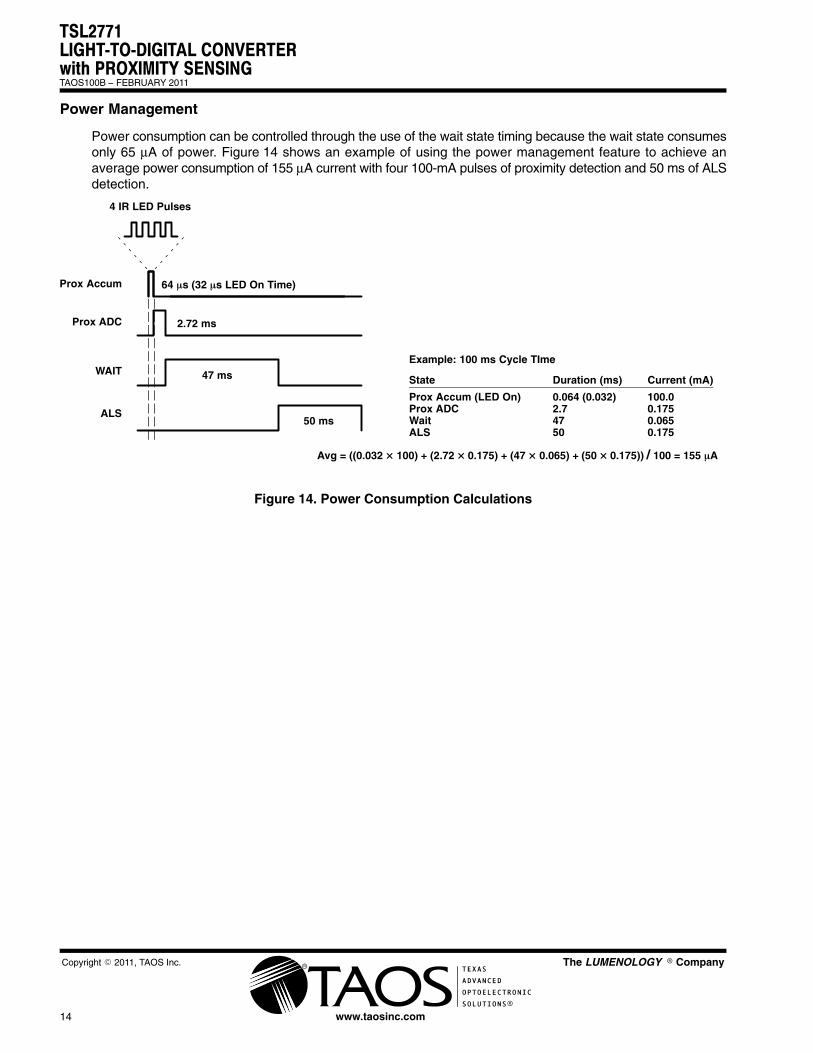
Power Management
Power consumption can be controlled through the use of the wait state timing because the wait state consumesonly 65 μA of power. Figure 14 shows an example of using the power management feature to achieve anaverage power consumption of 155 μA current with four 100-mA pulses of proximity detection and 50 ms of ALSdetection.
4 IR LED Pulses
64 �s (32 �s LED On Time)
2.72 ms
47 ms
50 ms
Prox ADC
Prox Accum
WAIT
ALS
Avg = ((0.032 � 100) + (2.72 � 0.175) + (47 � 0.065) + (50 � 0.175)) / 100 = 155 �A
State Duration (ms) Current (mA)
Prox Accum (LED On) 0.064 (0.032) 100.0Prox ADC 2.7 0.175Wait 47 0.065ALS 50 0.175
Example: 100 ms Cycle TIme
Figure 14. Power Consumption Calculations

TSL2771
LIGHT-TO-DIGITAL CONVERTER
with PROXIMITY SENSINGTAOS100B − FEBRUARY 2011
15
The LUMENOLOGY � Company�
�
Copyright � 2011, TAOS Inc.
www.taosinc.com
I2C Protocol
Interface and control are accomplished through an I2C serial compatible interface (standard or fast mode) toa set of registers that provide access to device control functions and output data. The devices support the 7-bitI2C addressing protocol.
The I2C standard provides for three types of bus transaction: read, write, and a combined protocol (Figure 15).During a write operation, the first byte written is a command byte followed by data. In a combined protocol, thefirst byte written is the command byte followed by reading a series of bytes. If a read command is issued, theregister address from the previous command will be used for data access. Likewise, if the MSB of the commandis not set, the device will write a series of bytes at the address stored in the last valid command with a registeraddress. The command byte contains either control information or a 5-bit register address. The controlcommands can also be used to clear interrupts.
The I2C bus protocol was developed by Philips (now NXP). For a complete description of the I2C protocol, pleasereview the NXP I2C design specification at http://www.i2c−bus.org/references/.
A Acknowledge (0)N Not Acknowledged (1)P Stop ConditionR Read (1)S Start ConditionS Repeated Start ConditionW Write (0)... Continuation of protocol Master-to-Slave Slave-to-Master
W
7
Data ByteSlave AddressS
1
A AA
81 1 1 8
Command Code
1
P
1
...
I2C Write Protocol
I2C Read Protocol
I2C Read Protocol — Combined Format
R
7
DataSlave AddressS
1
A AA
81 1 1 8
Data
1
P
1
...
W
7
Slave AddressSlave AddressS
1
A RA
81 1 1 7 1 1
Command Code S
1
A
Data AA
8 1 8
Data
1
P
1
...
Figure 15. I2C Protocols

TSL2771
LIGHT-TO-DIGITAL CONVERTER
with PROXIMITY SENSINGTAOS100B − FEBRUARY 2011
16
�
�
Copyright � 2011, TAOS Inc. The LUMENOLOGY � Company
www.taosinc.com
Register Set
The TSL2771 is controlled and monitored by data registers and a command register accessed through the serialinterface. These registers provide for a variety of control functions and can be read to determine results of theADC conversions. The register set is summarized in Table 1.
Table 1. Register Address
ADDRESS RESISTER NAME R/W REGISTER FUNCTION RESET VALUE
−− COMMAND W Specifies register address 0x00
0x00 ENABLE R/W Enables states and interrupts 0x00
0x01 ATIME R/W ALS ADC time 0xFF
0x02 PTIME R/W Proximity ADC time 0xFF
0x03 WTIME R/W Wait time 0xFF
0x04 AILTL R/W ALS interrupt low threshold low byte 0x00
0x05 AILTH R/W ALS interrupt low threshold high byte 0x00
0x06 AIHTL R/W ALS interrupt high threshold low byte 0x00
0x07 AIHTH R/W ALS interrupt high threshold high byte 0x00
0x08 PILTL R/W Proximity interrupt low threshold low byte 0x00
0x09 PILTH R/W Proximity interrupt low threshold high byte 0x00
0x0A PIHTL R/W Proximity interrupt high threshold low byte 0x00
0x0B PIHTH R/W Proximity interrupt high threshold high byte 0x00
0x0C PERS R/W Interrupt persistence filters 0x00
0x0D CONFIG R/W Configuration 0x00
0x0E PPCOUNT R/W Proximity pulse count 0x00
0x0F CONTROL R/W Control register 0x00
0x12 ID R Device ID ID
0x13 STATUS R Device status 0x00
0x14 C0DATA R CH0 ADC low data register 0x00
0x15 C0DATAH R CH0 ADC high data register 0x00
0x16 C1DATA R CH1 ADC low data register 0x00
0x17 C1DATAH R CH1 ADC high data register 0x00
0x18 PDATA R Proximity ADC low data register 0x00
0x19 PDATAH R Proximity ADC high data register 0x00
The mechanics of accessing a specific register depends on the specific protocol used. See the section on I2Cprotocols on the previous pages. In general, the COMMAND register is written first to specify the specificcontrol/status register for following read/write operations.

TSL2771
LIGHT-TO-DIGITAL CONVERTER
with PROXIMITY SENSINGTAOS100B − FEBRUARY 2011
17
The LUMENOLOGY � Company�
�
Copyright � 2011, TAOS Inc.
www.taosinc.com
Command Register
The command registers specifies the address of the target register for future write and read operations.
Table 2. Command Register
67 5 4
ADD
23 1 0
COMMAND COMMAND TYPE − −
FIELD BITS DESCRIPTION
COMMAND 7 Select Command Register. Must write as 1 when addressing COMMAND register.
TYPE 6:5 Selects type of transaction to follow in subsequent data transfers:
FIELD VALUE DESCRIPTION
00 Repeated byte protocol transaction
01 Auto-increment protocol transaction
10 Reserved — Do not use
11 Special function — See description below
Transaction type 00 will repeatedly read the same register with each data access.Transaction type 01 will provide an auto-increment function to read successive register bytes.
ADD 4:0 Address register/special function field. Depending on the transaction type, see above, this field eitherspecifies a special function command or selects the specific control-status-register for the following writeand read transactions. The field values listed below apply only to special function commands:
FIELD VALUE DESCRIPTION
00000 Normal — no action
00101 Proximity interrupt clear
00110 ALS interrupt clear
00111 Proximity and ALS interrupt clear
other Reserved — Do not write
ALS/Proximity Interrupt Clear clears any pending ALS/Proximity interrupt. This special function is selfclearing.

TSL2771
LIGHT-TO-DIGITAL CONVERTER
with PROXIMITY SENSINGTAOS100B − FEBRUARY 2011
18
�
�
Copyright � 2011, TAOS Inc. The LUMENOLOGY � Company
www.taosinc.com
Enable Register (0x00)
The ENABLE register is used to power the device on/off, enable functions, and interrupts.
Table 3. Enable Register
67 5 4
PON
23 1 0
ENABLE Reserved Resv AIEN Address0x00AENPIEN WEN PEN
FIELD BITS DESCRIPTION
Reserved 7:6 Reserved. Write as 0.
PIEN 5 Proximity interrupt mask. When asserted, permits proximity interrupts to be generated.
AIEN 4 ALS interrupt mask. When asserted, permits ALS interrupts to be generated.
WEN 3 Wait Enable. This bit activates the wait feature. Writing a 1 activates the wait timer. Writing a 0 disables thewait timer.
PEN 2 Proximity enable. This bit activates the proximity function. Writing a 1 enables proximity. Writing a 0disables proximity.
AEN 1 ALS Enable. This bit actives the two channel ADC. Writing a 1 activates the ALS. Writing a 0 disablesthe ALS.
PON 1, 2 0 Power ON. This bit activates the internal oscillator to permit the timers and ADC channels to operate.Writing a 1 activates the oscillator. Writing a 0 disables the oscillator.
NOTES: 1. See Power Management section for more information.2. A minimum interval of 2.72 ms must pass after PON is asserted before either a proximity or ALS can be initiated. This required time
is enforced by the hardware in cases where the firmware does not provide it.

TSL2771
LIGHT-TO-DIGITAL CONVERTER
with PROXIMITY SENSINGTAOS100B − FEBRUARY 2011
19
The LUMENOLOGY � Company�
�
Copyright � 2011, TAOS Inc.
www.taosinc.com
ALS Timing Register (0x01)
The ALS timing register controls the internal integration time of the ALS channel ADCs in 2.72 ms increments.
Table 4. ALS Timing Register
FIELD BITS DESCRIPTION
ATIME 7:0 VALUE INTEG_CYCLES TIME MAX COUNT
0xFF 1 2.72 ms 1024
0xF6 10 27.2 ms 10240
0xDB 37 101 ms 37888
0xC0 64 174 ms 65535
0x00 256 696 ms 65535
Proximity Time Control Register (0x02)
The proximity timing register controls the integration time of the proximity ADC in 2.72 ms increments. It isrecommended that this register be programmed to a value of 0xFF (1 integration cycle).
Table 5. Proximity Time Control Register
FIELD BITS DESCRIPTION
PTIME 7:0 VALUE INTEG_CYCLES TIME MAX COUNT
0xFF 1 2.72 ms 1023
Wait Time Register (0x03)
Wait time is set 2.72 ms increments unless the WLONG bit is asserted in which case the wait times are 12×longer. WTIME is programmed as a 2’s complement number.
Table 6. Wait Time Register
FIELD BITS DESCRIPTION
WTIME 7:0 REGISTER VALUE WAIT TIME TIME (WLONG = 0) TIME (WLONG = 1)
0xFF 1 2.72 ms 0.032 sec
0xB6 74 201 ms 2.4 sec
0x00 256 696 ms 8.3 sec
NOTE: The Proximity Wait Time Register should be configured before PEN and/or AEN is/are asserted.

TSL2771
LIGHT-TO-DIGITAL CONVERTER
with PROXIMITY SENSINGTAOS100B − FEBRUARY 2011
20
�
�
Copyright � 2011, TAOS Inc. The LUMENOLOGY � Company
www.taosinc.com
ALS Interrupt Threshold Registers (0x04 − 0x07)
The ALS interrupt threshold registers provides the values to be used as the high and low trigger points for thecomparison function for interrupt generation. If C0DATA crosses below the low threshold specified, or abovethe higher threshold, an interrupt is asserted on the interrupt pin.
Table 7. ALS Interrupt Threshold Register
REGISTER ADDRESS BITS DESCRIPTION
AILTL 0x04 7:0 ALS low threshold lower byte
AILTH 0x05 7:0 ALS low threshold upper byte
AIHTL 0x06 7:0 ALS high threshold lower byte
AIHTH 0x07 7:0 ALS high threshold upper byte
Proximity Interrupt Threshold Registers (0x08 − 0x0B)
The proximity interrupt threshold registers provide the values to be used as the high and low trigger points forthe comparison function for interrupt generation. If the value generated by proximity channel crosses below thelower threshold specified, or above the higher threshold, an interrupt is signaled to the host processor.
Table 8. Proximity Interrupt Threshold Register
REGISTER ADDRESS BITS DESCRIPTION
PILTL 0x08 7:0 Proximity low threshold lower byte
PILTH 0x09 7:0 Proximity low threshold upper byte
PIHTL 0x0A 7:0 Proximity high threshold lower byte
PIHTH 0x0B 7:0 Proximity high threshold upper byte

TSL2771
LIGHT-TO-DIGITAL CONVERTER
with PROXIMITY SENSINGTAOS100B − FEBRUARY 2011
21
The LUMENOLOGY � Company�
�
Copyright � 2011, TAOS Inc.
www.taosinc.com
Persistence Register (0x0C)
The persistence register controls the filtering interrupt capabilities of the device. Configurable filtering isprovided to allow interrupts to be generated after each ADC integration cycle or if the ADC integration hasproduced a result that is outside of the values specified by threshold register for some specified amount of time.Separate filtering is provided for proximity and ALS functions. ALS interrupts are generated using C0DATA.
Table 9. Persistence Register
67 5 4
APERS
23 1 0
PERS PPERSAddress0x0C
FIELD BITS DESCRIPTION
PPERS 7:4 Proximity interrupt persistence. Controls rate of proximity interrupt to the host processor.
FIELD VALUE MEANING INTERRUPT PERSISTENCE FUNCTION
0000 −−− Every proximity cycle generates an interrupt
0001 1 1 proximity value out of range
0010 2 2 consecutive proximity values out of range
... ... ...
1111 15 15 consecutive proximity values out of range
APERS 3:0 Interrupt persistence. Controls rate of interrupt to the host processor.
FIELD VALUE MEANING INTERRUPT PERSISTENCE FUNCTION
0000 Every Every ALS cycle generates an interrupt
0001 1 1 value outside of threshold range
0010 2 2 consecutive values out of range
0011 3 3 consecutive values out of range
0100 5 5 consecutive values out of range
0101 10 10 consecutive values out of range
0110 15 15 consecutive values out of range
0111 20 20 consecutive values out of range
1000 25 25 consecutive values out of range
1001 30 30 consecutive values out of range
1010 35 35 consecutive values out of range
1011 40 40 consecutive values out of range
1100 45 45 consecutive values out of range
1101 50 50 consecutive values out of range
1110 55 55 consecutive values out of range
1111 60 60 consecutive values out of range

TSL2771
LIGHT-TO-DIGITAL CONVERTER
with PROXIMITY SENSINGTAOS100B − FEBRUARY 2011
22
�
�
Copyright � 2011, TAOS Inc. The LUMENOLOGY � Company
www.taosinc.com
Configuration Register (0x0D)
The configuration register sets the wait long time.
Table 10. Configuration Register
67 5 4 23 1 0
CONFIG Reserved WLONGAddress0x0DReserved
FIELD BITS DESCRIPTION
Reserved 7:2 Reserved. Write as 0.
WLONG 1 Wait Long. When asserted, the wait cycles are increased by a factor 12× from that programmed in theWTIME register.
Reserved 0 Reserved. Write as 0.
Proximity Pulse Count Register (0x0E)
The proximity pulse count register sets the number of proximity pulses that will be transmitted. When proximitydetection is enabled, a proximity detect cycle occurs after each ALS cycle. PPULSE defines the number ofpulses to be transmitted at a 62.5-kHz rate.
NOTE: The ATIME register will be used to time the interval between proximity detection events even if the ALSfunction is disabled.
Table 11. Proximity Pulse Count Register
67 5 4 23 1 0
PPULSE PPULSEAddress0x0E
FIELD BITS DESCRIPTION
PPULSE 7:0 Proximity Pulse Count. Specifies the number of proximity pulses to be generated.

TSL2771
LIGHT-TO-DIGITAL CONVERTER
with PROXIMITY SENSINGTAOS100B − FEBRUARY 2011
23
The LUMENOLOGY � Company�
�
Copyright � 2011, TAOS Inc.
www.taosinc.com
Control Register (0x0F)
The Control register provides eight bits of miscellaneous control to the analog block. These bits typically controlfunctions such as gain settings and/or diode selection.
Table 12. Control Register
67 5 4 23 1 0
CONTROL PDRIVE ResvAddress0x0FPDIODE Reserved AGAIN
FIELD BITS DESCRIPTION
PDRIVE 7:6 LED Drive Strength.
FIELD VALUE LED STRENGTH
00 100 mA
01 50 mA
10 25 mA
11 12.5 mA
PDIODE 5:4 Proximity Diode Select.
FIELD VALUE DIODE SELECTION
00 Reserved
01 Proximity uses the CH0 diode
10 Proximity uses the CH1 diode
11 Proximity uses both diodes
Reserved 3:2 Reserved. Write bits as zero (0:0)
AGAIN 1:0 ALS Gain Control.
FIELD VALUE ALS GAIN VALUE
00 1× gain
01 8× gain
10 16× gain
11 120× gain
ID Register (0x12)
The ID Register provides the value for the part number. The ID register is a read-only register.
Table 13. ID Register
67 5 4 23 1 0
ID IDAddress0x12
FIELD BITS DESCRIPTION
ID 7:0 Part number identification0x00 = TSL27711 & TSL27715
ID 7:0 Part number identification0x09 = TSL27713 & TSL27717
TSL2771
LIGHT-TO-DIGITAL CONVERTER
with PROXIMITY SENSINGTAOS100B − FEBRUARY 2011
24
�
�
Copyright � 2011, TAOS Inc. The LUMENOLOGY � Company
www.taosinc.com
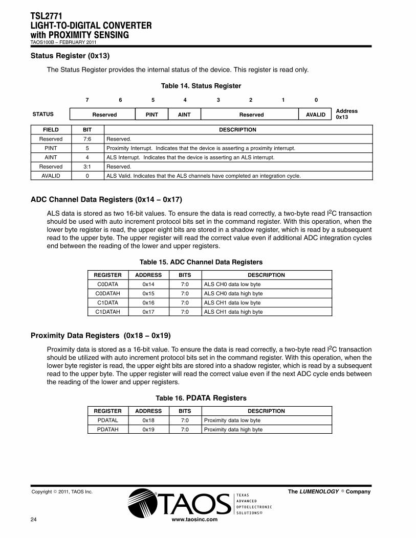
Status Register (0x13)
The Status Register provides the internal status of the device. This register is read only.
Table 14. Status Register
67 5 4
AVALID
23 1 0
STATUS Reserved Resv AINTAddress0x13ReservedPINT
FIELD BIT DESCRIPTION
Reserved 7:6 Reserved.
PINT 5 Proximity Interrupt. Indicates that the device is asserting a proximity interrupt.
AINT 4 ALS Interrupt. Indicates that the device is asserting an ALS interrupt.
Reserved 3:1 Reserved.
AVALID 0 ALS Valid. Indicates that the ALS channels have completed an integration cycle.
ADC Channel Data Registers (0x14 − 0x17)
ALS data is stored as two 16-bit values. To ensure the data is read correctly, a two-byte read I2C transactionshould be used with auto increment protocol bits set in the command register. With this operation, when thelower byte register is read, the upper eight bits are stored in a shadow register, which is read by a subsequentread to the upper byte. The upper register will read the correct value even if additional ADC integration cyclesend between the reading of the lower and upper registers.
Table 15. ADC Channel Data Registers
REGISTER ADDRESS BITS DESCRIPTION
C0DATA 0x14 7:0 ALS CH0 data low byte
C0DATAH 0x15 7:0 ALS CH0 data high byte
C1DATA 0x16 7:0 ALS CH1 data low byte
C1DATAH 0x17 7:0 ALS CH1 data high byte
Proximity Data Registers (0x18 − 0x19)
Proximity data is stored as a 16-bit value. To ensure the data is read correctly, a two-byte read I2C transactionshould be utilized with auto increment protocol bits set in the command register. With this operation, when thelower byte register is read, the upper eight bits are stored into a shadow register, which is read by a subsequentread to the upper byte. The upper register will read the correct value even if the next ADC cycle ends betweenthe reading of the lower and upper registers.
Table 16. PDATA Registers
REGISTER ADDRESS BITS DESCRIPTION
PDATAL 0x18 7:0 Proximity data low byte
PDATAH 0x19 7:0 Proximity data high byte
TSL2771
LIGHT-TO-DIGITAL CONVERTER
with PROXIMITY SENSINGTAOS100B − FEBRUARY 2011
25
The LUMENOLOGY � Company�
�
Copyright � 2011, TAOS Inc.
www.taosinc.com
APPLICATION INFORMATION: HARDWARE
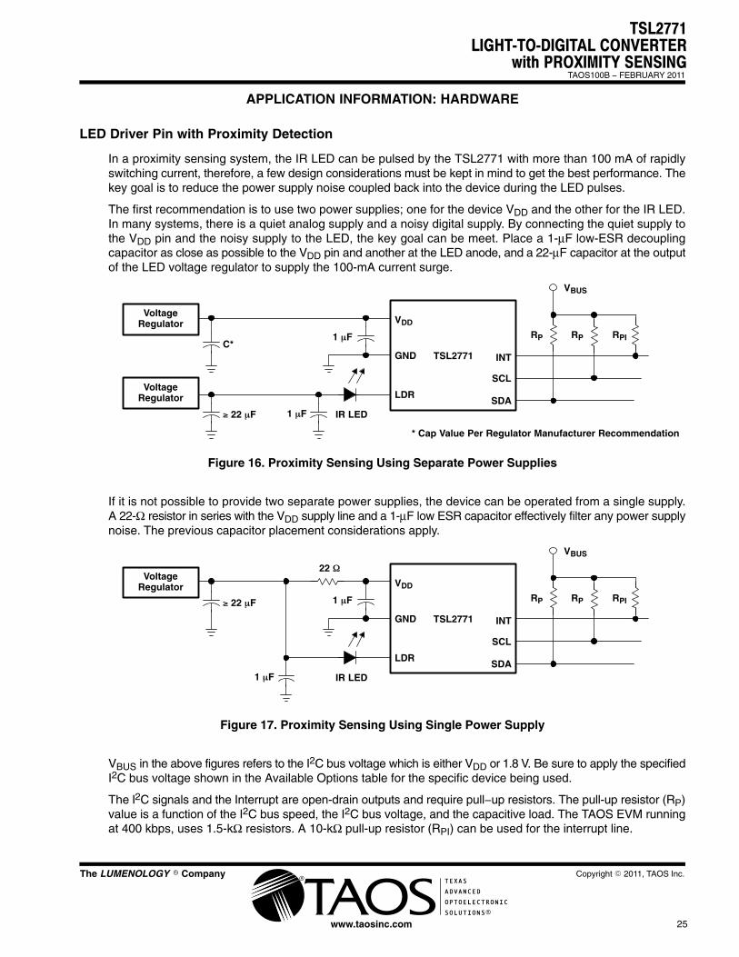
LED Driver Pin with Proximity Detection
In a proximity sensing system, the IR LED can be pulsed by the TSL2771 with more than 100 mA of rapidlyswitching current, therefore, a few design considerations must be kept in mind to get the best performance. Thekey goal is to reduce the power supply noise coupled back into the device during the LED pulses.
The first recommendation is to use two power supplies; one for the device VDD and the other for the IR LED.In many systems, there is a quiet analog supply and a noisy digital supply. By connecting the quiet supply tothe VDD pin and the noisy supply to the LED, the key goal can be meet. Place a 1-μF low-ESR decouplingcapacitor as close as possible to the VDD pin and another at the LED anode, and a 22-μF capacitor at the outputof the LED voltage regulator to supply the 100-mA current surge.
TSL2771 INT
SDA
SCL
VDD
LDR
1 �F
VoltageRegulator
VoltageRegulator
� 22 �F
* Cap Value Per Regulator Manufacturer Recommendation
IR LED
GND
VBUS
RP RP RPIC*
1 �F
Figure 16. Proximity Sensing Using Separate Power Supplies
If it is not possible to provide two separate power supplies, the device can be operated from a single supply.A 22-Ω resistor in series with the VDD supply line and a 1-μF low ESR capacitor effectively filter any power supplynoise. The previous capacitor placement considerations apply.
TSL2771 INT
SDA
SCL
VDD
LDR
1 �F
VoltageRegulator
� 22 �F
IR LED
GND
VBUS
RP RP RPI
1 �F
22 �
Figure 17. Proximity Sensing Using Single Power Supply
VBUS in the above figures refers to the I2C bus voltage which is either VDD or 1.8 V. Be sure to apply the specifiedI2C bus voltage shown in the Available Options table for the specific device being used.
The I2C signals and the Interrupt are open-drain outputs and require pull−up resistors. The pull-up resistor (RP)value is a function of the I2C bus speed, the I2C bus voltage, and the capacitive load. The TAOS EVM runningat 400 kbps, uses 1.5-kΩ resistors. A 10-kΩ pull-up resistor (RPI) can be used for the interrupt line.

TSL2771
LIGHT-TO-DIGITAL CONVERTER
with PROXIMITY SENSINGTAOS100B − FEBRUARY 2011
26
�
�
Copyright � 2011, TAOS Inc. The LUMENOLOGY � Company
www.taosinc.com
APPLICATION INFORMATION: HARDWARE
PCB Pad Layout
Suggested PCB pad layout guidelines for the Dual Flat No-Lead (FN) surface mount package are shown inFigure 18.
400
2500
400
1000
1700
650
1000
650
Note: Pads can beextended further if handsoldering is needed.
NOTES: A. All linear dimensions are in micrometers.B. This drawing is subject to change without notice.
Figure 18. Suggested FN Package PCB Layout
TSL2771
LIGHT-TO-DIGITAL CONVERTER
with PROXIMITY SENSINGTAOS100B − FEBRUARY 2011
27
The LUMENOLOGY � Company�
�
Copyright � 2011, TAOS Inc.
www.taosinc.com
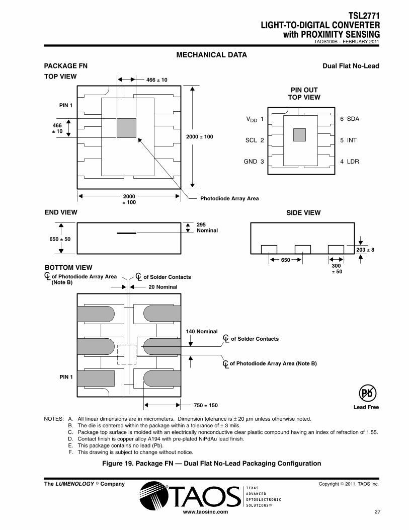
MECHANICAL DATAPACKAGE FN Dual Flat No-Lead
203 � 8
6 SDA
5 INT
4 LDR
VDD 1
SCL 2
GND 3
TOP VIEW
SIDE VIEW
BOTTOM VIEW
Lead Free
Pb
300� 50
650
2000� 100
2000 � 100
PIN 1
PIN 1
END VIEW
650 � 50
PIN OUTTOP VIEW
750 � 150
Photodiode Array Area
295Nominal
466� 10
466 � 10
CL of Solder ContactsCL of Photodiode Array Area(Note B)
20 Nominal
CL of Solder Contacts
of Photodiode Array Area (Note B)CL
140 Nominal
NOTES: A. All linear dimensions are in micrometers. Dimension tolerance is ± 20 μm unless otherwise noted.B. The die is centered within the package within a tolerance of ± 3 mils.C. Package top surface is molded with an electrically nonconductive clear plastic compound having an index of refraction of 1.55.D. Contact finish is copper alloy A194 with pre-plated NiPdAu lead finish.E. This package contains no lead (Pb).F. This drawing is subject to change without notice.
Figure 19. Package FN — Dual Flat No-Lead Packaging Configuration

TSL2771
LIGHT-TO-DIGITAL CONVERTER
with PROXIMITY SENSINGTAOS100B − FEBRUARY 2011
28
�
�
Copyright � 2011, TAOS Inc. The LUMENOLOGY � Company
www.taosinc.com
MECHANICAL DATA
TOP VIEW
DETAIL A
2.18 � 0.05Ao
0.254� 0.02
5� Max
4.00
8.00
3.50 � 0.05
� 1.504.00
2.00 � 0.05
+ 0.30− 0.10
1.75
B
BA A
� 1.00� 0.25
DETAIL B
2.18 � 0.05Bo
5� Max
0.83 � 0.05Ko
NOTES: A. All linear dimensions are in millimeters. Dimension tolerance is ± 0.10 mm unless otherwise noted.B. The dimensions on this drawing are for illustrative purposes only. Dimensions of an actual carrier may vary slightly.C. Symbols on drawing Ao, Bo, and Ko are defined in ANSI EIA Standard 481−B 2001.D. Each reel is 178 millimeters in diameter and contains 3500 parts.E. TAOS packaging tape and reel conform to the requirements of EIA Standard 481−B.F. In accordance with EIA standard, device pin 1 is located next to the sprocket holes in the tape.G. This drawing is subject to change without notice.
Figure 20. Package FN Carrier Tape

TSL2771
LIGHT-TO-DIGITAL CONVERTER
with PROXIMITY SENSINGTAOS100B − FEBRUARY 2011
29
The LUMENOLOGY � Company�
�
Copyright � 2011, TAOS Inc.
www.taosinc.com
MANUFACTURING INFORMATION
The FN package has been tested and has demonstrated an ability to be reflow soldered to a PCB substrate.
The solder reflow profile describes the expected maximum heat exposure of components during the solderreflow process of product on a PCB. Temperature is measured on top of component. The components shouldbe limited to a maximum of three passes through this solder reflow profile.
Table 17. Solder Reflow Profile
PARAMETER REFERENCE DEVICE
Average temperature gradient in preheating 2.5°C/sec
Soak time tsoak 2 to 3 minutes
Time above 217°C (T1) t1 Max 60 sec
Time above 230°C (T2) t2 Max 50 sec
Time above Tpeak −10°C (T3) t3 Max 10 sec
Peak temperature in reflow Tpeak 260°C
Temperature gradient in cooling Max −5°C/sec
t3t2t1tsoak
T3
T2
T1
TpeakNot to scale — for reference only
Time (sec)
Tem
per
atu
re (�C
)
Figure 21. Solder Reflow Profile Graph

TSL2771
LIGHT-TO-DIGITAL CONVERTER
with PROXIMITY SENSINGTAOS100B − FEBRUARY 2011
30
�
�
Copyright � 2011, TAOS Inc. The LUMENOLOGY � Company
www.taosinc.com
MANUFACTURING INFORMATION
Moisture Sensitivity
Optical characteristics of the device can be adversely affected during the soldering process by the release andvaporization of moisture that has been previously absorbed into the package. To ensure the package containsthe smallest amount of absorbed moisture possible, each device is dry-baked prior to being packed for shipping.Devices are packed in a sealed aluminized envelope called a moisture barrier bag with silica gel to protect themfrom ambient moisture during shipping, handling, and storage before use.
The FN package has been assigned a moisture sensitivity level of MSL 3 and the devices should be stored underthe following conditions:
Temperature Range 5°C to 50°CRelative Humidity 60% maximumTotal Time 12 months from the date code on the aluminized envelope — if unopenedOpened Time 168 hours or fewer
Rebaking will be required if the devices have been stored unopened for more than 12 months or if the aluminizedenvelope has been open for more than 168 hours. If rebaking is required, it should be done at 50°C for 12 hours.

TSL2771
LIGHT-TO-DIGITAL CONVERTER
with PROXIMITY SENSINGTAOS100B − FEBRUARY 2011
31
The LUMENOLOGY � Company�
�
Copyright � 2011, TAOS Inc.
www.taosinc.com
PRODUCTION DATA — information in this document is current at publication date. Products conform tospecifications in accordance with the terms of Texas Advanced Optoelectronic Solutions, Inc. standardwarranty. Production processing does not necessarily include testing of all parameters.
LEAD-FREE (Pb-FREE) and GREEN STATEMENTPb-Free (RoHS) TAOS’ terms Lead-Free or Pb-Free mean semiconductor products that are compatible with the currentRoHS requirements for all 6 substances, including the requirement that lead not exceed 0.1% by weight in homogeneousmaterials. Where designed to be soldered at high temperatures, TAOS Pb-Free products are suitable for use in specifiedlead-free processes.
Green (RoHS & no Sb/Br) TAOS defines Green to mean Pb-Free (RoHS compatible), and free of Bromine (Br) andAntimony (Sb) based flame retardants (Br or Sb do not exceed 0.1% by weight in homogeneous material).
Important Information and Disclaimer The information provided in this statement represents TAOS’ knowledge andbelief as of the date that it is provided. TAOS bases its knowledge and belief on information provided by third parties,and makes no representation or warranty as to the accuracy of such information. Efforts are underway to better integrateinformation from third parties. TAOS has taken and continues to take reasonable steps to provide representativeand accurate information but may not have conducted destructive testing or chemical analysis on incoming materials andchemicals. TAOS and TAOS suppliers consider certain information to be proprietary, and thus CAS numbers and otherlimited information may not be available for release.
NOTICETexas Advanced Optoelectronic Solutions, Inc. (TAOS) reserves the right to make changes to the products contained in thisdocument to improve performance or for any other purpose, or to discontinue them without notice. Customers are advisedto contact TAOS to obtain the latest product information before placing orders or designing TAOS products into systems.
TAOS assumes no responsibility for the use of any products or circuits described in this document or customer productdesign, conveys no license, either expressed or implied, under any patent or other right, and makes no representation thatthe circuits are free of patent infringement. TAOS further makes no claim as to the suitability of its products for any particularpurpose, nor does TAOS assume any liability arising out of the use of any product or circuit, and specifically disclaims anyand all liability, including without limitation consequential or incidental damages.
TEXAS ADVANCED OPTOELECTRONIC SOLUTIONS, INC. PRODUCTS ARE NOT DESIGNED OR INTENDED FORUSE IN CRITICAL APPLICATIONS IN WHICH THE FAILURE OR MALFUNCTION OF THE TAOS PRODUCT MAYRESULT IN PERSONAL INJURY OR DEATH. USE OF TAOS PRODUCTS IN LIFE SUPPORT SYSTEMS IS EXPRESSLYUNAUTHORIZED AND ANY SUCH USE BY A CUSTOMER IS COMPLETELY AT THE CUSTOMER’S RISK.
LUMENOLOGY, TAOS, the TAOS logo, and Texas Advanced Optoelectronic Solutions are registered trademarks of Texas AdvancedOptoelectronic Solutions Incorporated.

TSL2771
LIGHT-TO-DIGITAL CONVERTER
with PROXIMITY SENSINGTAOS100B − FEBRUARY 2011
32
�
�
Copyright � 2011, TAOS Inc. The LUMENOLOGY � Company
www.taosinc.com


