
Tunable van Hove Singularities and Correlated States in Twisted
Trilayer Graphene
Yanmeng Shi1,2,†, Shuigang Xu2,†, Mohammed M. Al Ezzi3,†, Nilanthy Balakrishnan2,†, Aitor Garcia-
Ruiz1,2, Bonnie Tsim1,2, Ciaran Mullan1, Julien Barrier1,2, Na Xin2, Benjamin A. Piot4, Takashi Taniguchi5,
Kenji Watanabe5, Alexandra Carvalho3, Artem Mishchenko1,2, A. K. Geim1,2, Vladimir I. Fal’ko1,2,6,
Shaffique Adam3,7, Antonio Helio Castro Neto3, Kostya S. Novoselov1,2,3,8,*
1Department of Physics and Astronomy, University of Manchester, Manchester M13 9PL, UK. 2National Graphene Institute, University of Manchester, Manchester M13 9PL, UK.
3Centre for Advanced 2D Materials, National University of Singapore, 117546, Singapore 4Laboratoire National des Champs Magnétiques Intenses, LNCMI-CNRS-UGA-UPS-INSA-EMFL, 25 avenue
des Martyrs, 38042 Grenoble, France. 5National Institute for Materials Science, 1-1 Namiki, Tsukuba, 305-0044, Japan.
6Henry Royce Institute for Advanced Materials, Manchester, M13 9PL, UK. 7Yale-NUS College, 16 College Avenue West, 138527 Singapore.
8Chongqing 2D Materials Institute, Liangjiang New Area, Chongqing 400714, China †These authors contributed equally *e-mail: [email protected]
Abstract
Understanding and tuning correlated states is of great interest and significance to modern condensed matter physics. The recent discovery of unconventional superconductivity and Mott-like insulating states in magic-angle twisted bilayer graphene (tBLG) presents a unique platform to study correlation phenomena, in which the Coulomb energy dominates over the quenched kinetic energy as a result of hybridized flat bands. Extending this approach to the case of twisted multilayer graphene would allow even higher control over the band structure because of the reduced symmetry of the system. Here, we study electronic transport properties in twisted trilayer graphene (tTLG, bilayer on top of monolayer graphene heterostructure). We observed the formation of van Hove singularities which are highly tunable by twist angle and displacement field and can cause strong correlation effects under optimum conditions, including superconducting states. We provide basic theoretical interpretation of the observed electronic structure.
Van der Waals heterostructures technology provides a variety of tuning knobs, including
twist angle, displacement field, and stacking order, for band engineering by precise stacking of one
atomically thin crystal onto another1. The lattice constant mismatch and relative twist angle give rise
to a moiré superlattice, where, under some conditions, interlayer hybridization leads to the
formation of an isolated low energy flat band, which quenches the kinetic energy of electronic
system. Such low-energy subbands have been realised in several structures and emergent
phenomena have been reported, including Mott-like insulators2, unconventional superconductivity3-5
and ferromagnetism6,7 in twisted bilayer graphene (tBLG) and twisted double bilayer graphene
(tDBLG)8-11. Similar correlated states have also been reported in ABC-trilayer graphene (TLG)
superlattice on hexagonal boron nitride (hBN) and rhombohedral stacked graphite films12-14.
In this work, we study small-angle twisted trilayer graphene (tTLG) van der Waals
heterostructures, where a monolayer graphene (MLG) and bilayer graphene (BLG) are stacked and
rotated by a small angle with respect to each other. Compared to tBLG, more tuning knobs are
expected in tTLG, since the band structures in multi-layer graphene are more tunable than that of
the monolayer counterpart15-18. In particular, there naturally exists two stacking orders in trilayer
graphene, Bernal (ABA)-stacking with mirror symmetry and rhombohedral (ABC)-stacking with
inversion symmetry. The former is semimetallic, while the latter is known to be semiconducting with

a band gap tunable with an out-of-plane displacement field19. The symmetry is further reduced in
tTLG, by stacking mono- and bi-layer graphene together with a small relative twist angle20,21,
resulting into ABA-, ABB- and ABC-stacked domains. In this report, we observed electron-hole
asymmetry, tunable van Hove singularities as well as correlated insulating states at commensurate
fillings on the electron side under finite displacement field in tTLG. The correlated states are
asymmetric with respect to D, and highly tunable with varying twist angle. In addition, we observed
superconductivity signatures in the vicinity of the quarter-filling insulating state. tTLG can be seen as
a model system to understand emergent phenomena in the field of twistronics, with twist angle,
displacement field and charge density as tuning parameters.
Our twisted graphene heterostructures encapsulated in hBN flakes are fabricated using the
recently developed ‘tear & stack’ method22,23. We select the exfoliated graphene flakes with
monolayer/bilayer steps to ensure the precise orientation between the two crystals. We use the
dual-gate configuration as shown in Fig. 1b, to allow independent tuning of the carrier density n and
transverse displacement field D. By simultaneously applying the top and bottom gate voltages, we
obtain 𝑛 =𝑉𝑡𝑔𝐶𝑡𝑔+𝑉𝑏𝑔𝐶𝑏𝑔
𝑒and 𝐷 =
𝑉𝑏𝑔𝐶𝑏𝑔−𝑉𝑡𝑔𝐶𝑡𝑔
2 0, where 𝐶𝑡𝑔 and 𝐶𝑏𝑔 are the top and bottom gate
capacitances (normalised to unit area) measured from the Hall effect, 𝑒 is the electron charge, and
휀0 is the vacuum permittivity, respectively. The twist angles are determined by the charge density at
full filling of each sub-band and the Brown-Zak oscillations24 (Fig. s3). We have studied more than
half a dozen samples with different twist angles ranging between 1.22o and 1.6o. Here we mainly
focus on two samples, S1 with twist angle ≈1.47o and S2 with ≈1.22o.
The schematic of moiré superlattice with a relative twist angle in tTLG, together with the
schematics of the transport measurements are presented in Fig. 1a,b. The electronic band structures
of mono- and bi-layer graphene hybridize and fold into mini Brillouin zone (MBZ). The size of the
moiré unit cell is given by 𝜆 =𝑎
2𝑠𝑖𝑛𝜃
2
, where a=0.246 nm is the lattice constant of graphene, and
the area of moiré unit cell is 𝐴 =√3
2𝜆2. Each superlattice band in the MBZ can accommodate charge
density 𝑛0 =4
𝐴 , where the prefactor 4 is because of spin and valley degeneracies in graphene and
the filling factor is defined as n/n0.
The transport behaviour of our samples is presented in Fig. 1c-g, which display xx(n/n0,D)
maps for samples with from 1.22o to 1.6o, and n is normalized to the full-filling charge density
𝑛0 =8
√3𝜆2 , associated with the corresponding twist angle . Note that tTLG can be fabricated in two
mirror-symmetric configurations, either with BLG on top or MLG on top. When we compare the
samples with mirror-symmetric configurations, the overall picture flipped (see Fig. s1) which
demonstrates that the structure of the states we observe is not an artefact. Therefore, the
asymmetry with respect to D could be related to the lack of symmetry in tTLG21. To be consistent, we
define positive D when electric fields point from monolayer to bilayer graphene (see Fig. s1).
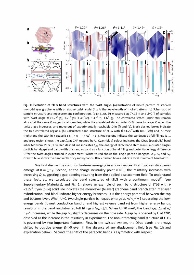
Fig. 1: Evolution of tTLG band structures with the twist angle. (a)Illustration of moiré pattern of stacked
mono-bilayer graphene with a relative twist angle θ. λ is the wavelength of moiré pattern. (b) Schematic of
sample structure and measurement configuration. (c-g) ρxx(n, D) measured at T=1.6 K and B=0 T of samples
with twist angle θ ≈1.22o
(c), 1.26o
(d), 1.41o
(e), 1.47o
(f), 1.6o
(g). The correlated states under D>0 remain
almost at the same D range for all samples, while the correlated states under D<0 move to larger D when the
twist angle increases, and move out of experimentally reachable D in (f) and (g). Black dashed boxes indicate
the two correlated regions. (h) Calculated band structure of tTLG with θ ≈1.22o
with U=0 (left) and 70 meV
(right) and the path in k-space is ( 𝛤 ⟶ 𝑀 ⟶ 𝐾/𝐾′ ⟶ 𝛤 ). Red regions indicate the bandgaps at full fillings 1,
and grey region shows the gap 0 at CNP opened by U. Cyan (blue) colour indicates the Dirac (parabolic) band
inherited from MLG (BLG). Red dashed line indicates EDS, the energy of Dirac band shift. (i-m) Calculated single-
particle bandgaps and bandwidth of c1 and v1 band as a function of band filling and potential energy difference
U for the twist angles studied in experiment. White to red shows the single-particle bangaps, -1, 0 and 1.
Grey to blue shows the bandwidth of c1 and v1 bands. Black dashed boxes indicate local minima of bandwidth.
We first discuss the common features emerging in all our devices. First, two resistive peaks
emerge at 𝑛 = ±𝑛0. Second, at the charge neutrality point (CNP), the resistivity increases with
increasing D, suggesting a gap opening resulting from the applied displacement field. To understand
these features, we calculated the band structures of tTLG with a continuum model25 (see
Supplementary Materials), and Fig. 1h shows an example of such band structure of tTLG with
≈1.22o. Cyan (blue) solid line indicates the monolayer (bilayer) graphene band branch after interlayer
hybridization, and black indicate higher energy branches. U is the energy potential between the top
and bottom layer. When U=0, two single-particle bandgaps emerge at 𝑛/𝑛0= ±1 separating the low-
energy bands (lowest conduction band c1 and highest valence band v1) from higher energy bands,
resulting in the band insulators at full fillings 𝑛/𝑛0 =±1. When U=70 meV, the band gap 1 at 𝑛/
𝑛0=1 increases, while the gap -1 slightly decreases on the hole side. A gap 0 is opened by U at CNP,
observed as the increase in the resistivity in experiment. The non-interacting band structure of tTLG
is governed by two important features. First, in the twisted system, the Dirac bands are always
shifted to positive energy EDS>0 even in the absence of any displacement field (see Fig. 1h and
explanation below). Second, the shift of the parabolic bands is asymmetric with respect
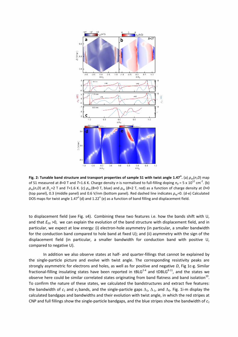
Fig. 2: Tunable band structure and transport properties of sample S1 with twist angle 1.47o. (a) ρxx(n,D) map
of S1 measured at B=0 T and T=1.6 K. Charge density n is normalised to full-filling doping n0 = 5 x 10¹²
cm-2
. (b)
ρxy(n,D) at 𝐵⊥=2 T and T=1.6 K. (c) ρxx (B=0 T, blue) and ρxy (B=2 T, red) as a function of charge density at D=0
(top panel), 0.3 (middle panel) and 0.6 V/nm (bottom panel). Red dashed line indicates ρxy=0. (d-e) Calculated
DOS maps for twist angle 1.47o
(d) and 1.22o (e) as a function of band filling and displacement field.
to displacement field (see Fig. s4). Combining these two features i.e. how the bands shift with U,
and that EDS >0, we can explain the evolution of the band structure with displacement field, and in
particular, we expect at low energy: (i) electron-hole asymmetry (in particular, a smaller bandwidth
for the conduction band compared to hole band at fixed U); and (ii) asymmetry with the sign of the
displacement field (in particular, a smaller bandwidth for conduction band with positive U,
compared to negative U).
In addition we also observe states at half- and quarter-fillings that cannot be explained by
the single-particle picture and evolve with twist angle. The corresponding resistivity peaks are
strongly asymmetric for electrons and holes, as well as for positive and negative D, Fig 1c-g. Similar
fractional-filling insulating states have been reported in tBLG2-4 and tDBLG8-11, and the states we
observe here could be similar correlated states originating from band flatness and band isolation10.
To confirm the nature of these states, we calculated the bandstructures and extract five features:
the bandwidth of c1 and v1 bands, and the single-particle gaps 1, -1, and 0. Fig. 1i-m display the
calculated bandgaps and bandwidths and their evolution with twist angle, in which the red stripes at
CNP and full fillings show the single-particle bandgaps, and the blue stripes show the bandwidth of c1

and v1 band. In Fig. 1i, two local bandwidth minima are present, as indicated by the black dashed
boxes. The bandwidth minimum of c1 band for U>0 increases with , consistent with the
experimental observation that the correlated feature on the positive D side fades away with
increasing . While for U<0, the position of minimum bandwidth of c1 band moves to larger U. As a
result, the flattest band moves out of D range that is experimentally achievable for twist angle
>1.41o, and becomes less isolated from higher conduction bands as 1 decreases with increasing U.
The electron-hole asymmetry could also be explained by the band flatness and band
isolation. For example, in Fig. 1i, the band width minimum of v1 band occurs when 80<U<120 meV,
where the gap -1 shrinks in the presence of U, meaning the v1 band is less isolated from lower
valence bands. With increasing angle, the v1 bandwidth minimum moves to higher U, and the gap -1
is closed. Therefore, the extracted features from our band structures calculation explain the
electron-hole asymmetry as well as why the correlated features are asymmetric with D, and absent
on negative D for samples with > 1.41o in the experiment. In fact, the asymmetric features of the
band structure is due to the Dirac energy shift20 where Dirac cone energy states originating from the
monolayer are shifted upward compared to the electronic state of the bilayer (Fig. 1h and Fig. s4).
We note that the displacement field has two effects on the band structure20. First, regardless of the
sign of the displacement field, it pushes the conduction band of the monolayer upwards and the
valence band downwards with equal magnitude. Second, for parabolic bands originating from the
bilayer graphene, a positive U shifts the conduction band upwards by U/2, as might be expected
from an isolated BLG, and the valence band downwards by U/6. This effect is reversed for negative
U. Notice, therefore, that for positive U, a bandgap at charge neutrality is opened up only after the
conduction band of the parabolic bilayer is shifted upwards by the displacement field U≥2EDS. The
resultant conduction band is very flat because the top of the moiré band is pinned at the Γ
point. The positive EDS also guarantees that the conduction bandwidth is flatter than the hole
bandwidth. For negative U, the band gap at charge neutrality is opened once U≥6EDS, and generically
the electron and hole bandwidths are larger than for positive U. These features can be clearly seen
in the numerical band structures shown in Fig. 1h and Fig. s4, calculated within the continuum model.
Fig. 2a shows the longitudinal resistivity xx of sample S1 as a function of n and D (n is
normalized to the full filling-charge density n0= 5 x 1012 cm-2, associated with a twist angle ≈1.47o).
The angle is confirmed by Brown-Zak oscillation (see Fig. s3). On the hole side, fractional filling
resistive peaks emerge in the whole range of D measured, and the position of this resistive peak
evolves with D. While on the electron side, resistive peaks only appear in a small range of D,
between 0.4-0.7 V/nm, and are absent for D<0, in contrast to the case of tDBLG10, in which the
correlated states are symmetric with respect to the sign of D.
To characterise the resistive peaks at fractional fillings, we study the response of the sample
in a perpendicular magnetic field. Fig. 2b shows the Hall resistivity at B=2 T, where sign changes are
present at CNP and at full fillings 𝑛 = ±𝑛0, in agreement with the presence of single-particle gaps
and change of charge type. Unexpectedly, xy also tends to change sign, i.e. Hall density resets, at
half filling n/n0=1/2 for 0.4<D<0.7 V/nm in Fig. 2b, which indicates the change of charge type from
hole-like to electron-like. Considering the metallic low resistivity (≈200 ) in this region, the change
of charge type at half filling could indicate the overlap between electron-like and hole-like bands,
suggesting new band edge formation as a result of electron correlations when each moiré unit cell
hosts 2 electrons.
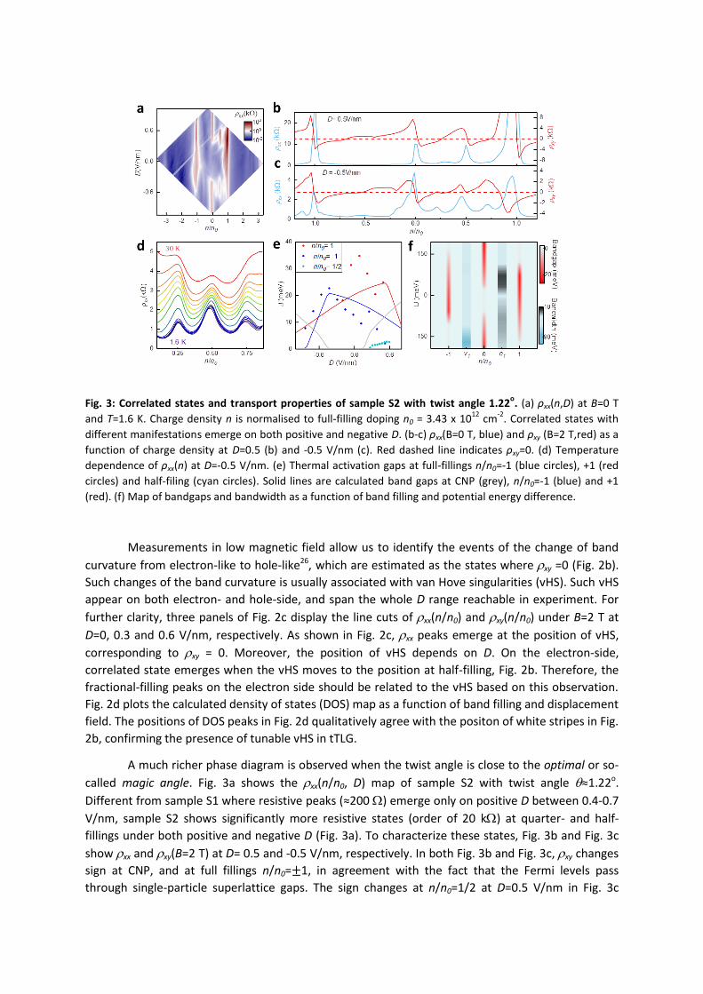
Fig. 3: Correlated states and transport properties of sample S2 with twist angle 1.22o. (a) ρxx(n,D) at B=0 T
and T=1.6 K. Charge density n is normalised to full-filling doping n0 = 3.43 x 10¹²
cm-2
. Correlated states with
different manifestations emerge on both positive and negative D. (b-c) ρxx(B=0 T, blue) and ρxy (B=2 T,red) as a
function of charge density at D=0.5 (b) and -0.5 V/nm (c). Red dashed line indicates ρxy=0. (d) Temperature
dependence of ρxx(n) at D=-0.5 V/nm. (e) Thermal activation gaps at full-fillings n/n0=-1 (blue circles), +1 (red
circles) and half-filing (cyan circles). Solid lines are calculated band gaps at CNP (grey), n/n0=-1 (blue) and +1
(red). (f) Map of bandgaps and bandwidth as a function of band filling and potential energy difference.
Measurements in low magnetic field allow us to identify the events of the change of band
curvature from electron-like to hole-like26, which are estimated as the states wherexy =0 (Fig. 2b).
Such changes of the band curvature is usually associated with van Hove singularities (vHS). Such vHS
appear on both electron- and hole-side, and span the whole D range reachable in experiment. For
further clarity, three panels of Fig. 2c display the line cuts of xx(n/n0) and xy(n/n0) under B=2 T at
D=0, 0.3 and 0.6 V/nm, respectively. As shown in Fig. 2c, xx peaks emerge at the position of vHS,
corresponding to xy = 0. Moreover, the position of vHS depends on D. On the electron-side,
correlated state emerges when the vHS moves to the position at half-filling, Fig. 2b. Therefore, the
fractional-filling peaks on the electron side should be related to the vHS based on this observation.
Fig. 2d plots the calculated density of states (DOS) map as a function of band filling and displacement
field. The positions of DOS peaks in Fig. 2d qualitatively agree with the positon of white stripes in Fig.
2b, confirming the presence of tunable vHS in tTLG.
A much richer phase diagram is observed when the twist angle is close to the optimal or so-
called magic angle. Fig. 3a shows the xx(n/n0, D) map of sample S2 with twist angle ≈1.22o.
Different from sample S1 where resistive peaks (≈200 ) emerge only on positive D between 0.4-0.7
V/nm, sample S2 shows significantly more resistive states (order of 20 k) at quarter- and half-
fillings under both positive and negative D (Fig. 3a). To characterize these states, Fig. 3b and Fig. 3c
show xx and xy(B=2 T) at D= 0.5 and -0.5 V/nm, respectively. In both Fig. 3b and Fig. 3c, xy changes
sign at CNP, and at full fillings n/n0=±1, in agreement with the fact that the Fermi levels pass
through single-particle superlattice gaps. The sign changes at n/n0=1/2 at D=0.5 V/nm in Fig. 3c

indicates the formation of a new Mott-like bandgap as a result of strong correlation. On the contrary,
at D=-0.5 V/nm, Hall density resettings appear at all commensurate fillings, indicating formations of
three new Fermi surfaces when c1 band hosts integer number of electrons. The amplitude of the
resistivity for the three states decreases with temperature (after background subtraction, see Fig. 3d,
as well as Fig. s2). Therefore, we attribute these three peaks to the correlation at commensurate
fillings, and the correlation weakens with increasing T. The relatively low resistivity and metallic
behaviour of the features at D<0 could be because the correlations cause band overlaps, rather than
open bandgaps when c1 band hosts integer number of electrons.
The correlated states manifesting themselves as resistive peaks at commensurate fillings
n/n0 = 1/4, 1/2, and 3/4, show qualitatively different behaviour for positive and negative D. The D>0
correlated states are more resistive (order of 20 k) than those on the D<0 side (<2.5 k), Fig. 3a.
The correlation is much stronger at half filling than at quarter and three-quarter fillings on the
positive D side, while on the negative D side, the resistive peaks are of the same order at all
commensurate fillings. The correlated states on the positive D side exhibit insulating behaviour,
while the negative side are metallic, as shown in Fig. 3d.
In tDBLG8-10, the correlated states at fractional fillings are attributed to the band flatness and
maximum isolation of the first electron c1 band from its neighbouring bands, and in tBLG2,3, spin and
valley degeneracy are broken as a result of strong correlation, giving rise to the correlated states at
integer number of electron/hole fillings. Fig. 3f shows the bandwidth of c1 and v1 bands, as well as
the bandgaps at CNP and n/n0=±1. Indeed, we find flattest c1 band occur at positive potential
difference 40<U<70 meV, where both the gaps at CNP and n/n0=1 are present. In addition, a local
minimum bandwidth also emerges for -120<U<-70 meV. The observation that the c1 band is flatter
when U>0 than that when U<0 agrees with the experimental observation that correlated states
under positive D are more robust than that under negative D. Fig. 3e displays the experimental
thermal activation gaps at n/n0=±1, and the calculated single-particle gaps as a function of D, which
qualitatively agree well with each other, confirming that the band isolation plays a role in the
correlation.
For a correlation mediated insulator, being close to commensuration is necessary but not
sufficient condition. Similar to tBLG, the origin of the strongly correlated insulator is not yet
understood. It could arise from the formation of a Mott insulator2, a Wigner crystal27, or because
the electron interactions lift the spin or valley degrees of freedom5. For all of these mechanisms, the
insulating state is expected to occur at commensurate fillings. This is because electron-electron
interactions conserve momentum, and can only dissipate current by the Umklapp processes that are
enabled when a moiré subband is completely filled28.
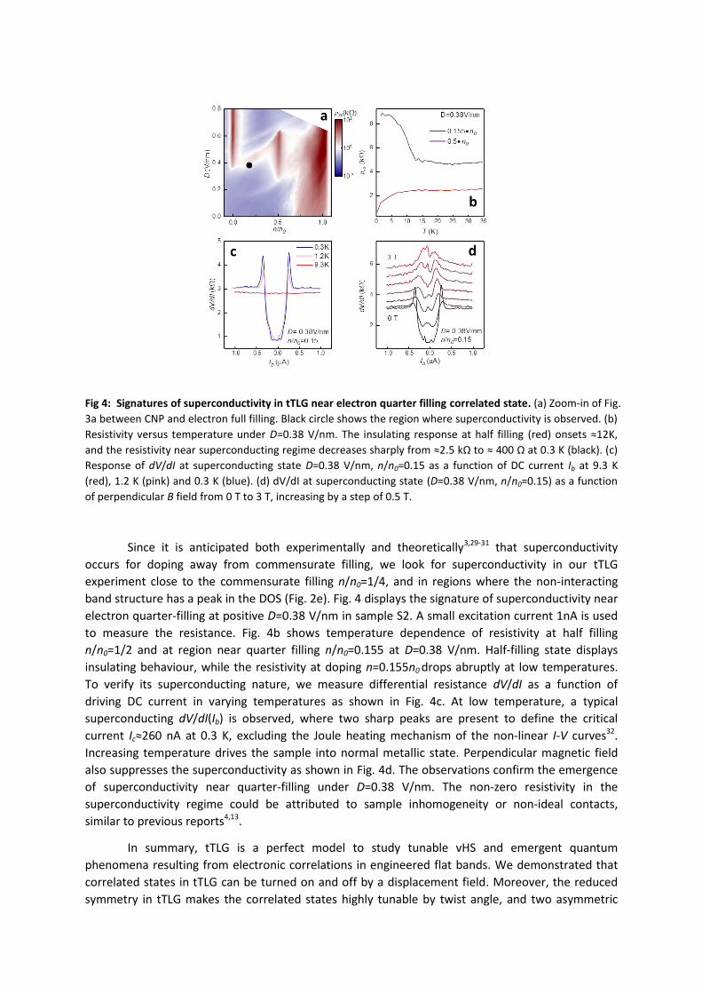
Fig 4: Signatures of superconductivity in tTLG near electron quarter filling correlated state. (a) Zoom-in of Fig.
3a between CNP and electron full filling. Black circle shows the region where superconductivity is observed. (b)
Resistivity versus temperature under D=0.38 V/nm. The insulating response at half filling (red) onsets ≈12K,
and the resistivity near superconducting regime decreases sharply from ≈2.5 kΩ to ≈ 400 Ω at 0.3 K (black). (c)
Response of dV/dI at superconducting state D=0.38 V/nm, n/n0=0.15 as a function of DC current Ib at 9.3 K
(red), 1.2 K (pink) and 0.3 K (blue). (d) dV/dI at superconducting state (D=0.38 V/nm, n/n0=0.15) as a function
of perpendicular B field from 0 T to 3 T, increasing by a step of 0.5 T.
Since it is anticipated both experimentally and theoretically3,29-31 that superconductivity
occurs for doping away from commensurate filling, we look for superconductivity in our tTLG
experiment close to the commensurate filling n/n0=1/4, and in regions where the non-interacting
band structure has a peak in the DOS (Fig. 2e). Fig. 4 displays the signature of superconductivity near
electron quarter-filling at positive D=0.38 V/nm in sample S2. A small excitation current 1nA is used
to measure the resistance. Fig. 4b shows temperature dependence of resistivity at half filling
n/n0=1/2 and at region near quarter filling n/n0=0.155 at D=0.38 V/nm. Half-filling state displays
insulating behaviour, while the resistivity at doping n=0.155n0 drops abruptly at low temperatures.
To verify its superconducting nature, we measure differential resistance dV/dI as a function of
driving DC current in varying temperatures as shown in Fig. 4c. At low temperature, a typical
superconducting dV/dI(Ib) is observed, where two sharp peaks are present to define the critical
current Ic≈260 nA at 0.3 K, excluding the Joule heating mechanism of the non-linear I-V curves32.
Increasing temperature drives the sample into normal metallic state. Perpendicular magnetic field
also suppresses the superconductivity as shown in Fig. 4d. The observations confirm the emergence
of superconductivity near quarter-filling under D=0.38 V/nm. The non-zero resistivity in the
superconductivity regime could be attributed to sample inhomogeneity or non-ideal contacts,
similar to previous reports4,13.
In summary, tTLG is a perfect model to study tunable vHS and emergent quantum
phenomena resulting from electronic correlations in engineered flat bands. We demonstrated that
correlated states in tTLG can be turned on and off by a displacement field. Moreover, the reduced
symmetry in tTLG makes the correlated states highly tunable by twist angle, and two asymmetric

correlated regions with respect to D are observed in our samples. In addition to the interesting
correlation physics, the Bernal (ABA) and rhombohedral (ABC) stacked domains in tTLG provide ideal
platforms to study topological edge states as ABA- and ABC-stacked few-layer graphene host totally
different band structures33. Our work thus paves the way for understanding the mechanism of
strong correlations in twistronics.
Methods
The heterostructures of twisted trilayer graphene encapsulated by hBN were assembled by
the standard dry-transfer and tear-and-stack techniques22 with a polypropylene carbonate (PPC) film
on top of a polydimethylsiloxane (PDMS) stamp. Graphene flake with monolayer/bilayer steps and
hBN flakes were exfoliated onto SiO2/Si substrate. After picking up a top hBN flake with the
PPC/PDMS stamp, we used the stack to tear and pick up the monolayer part of graphene flake from
the bilayer part at the temperature of 40 C. The remaining bilayer part on the substrate was then
rotated by a desired angle and subsequently picked up by the monolayer graphene/hBN stack. The
heterostructures were then released onto a bottom hBN exfoliated on 300 nm SiO2/doped Si
substrate to form hBN/monolayer Gr/bilayer Gr/hBN stack. The standard Hall bar geometry of the
devices was defined by e-beam lithography and etched by CHF3/O2 plasma. The one-dimensional
electrical contacts and top gate were deposited by e-beam evaporation of Cr/Au.
Transport measurements were performed in an either dry or liquid helium cryostat using
standard low-frequency AC measurement with Lock-in amplifiers. To detect the superconductivity,
the sample was loaded into 3He cryostat. Low temperature electrical filters were used to increase
the signal-to-noise ratio. The difference resistance dV/dI were measured by coupling a small AC
current (1 nA) and a DC current bias and measuring the differential voltage using lock-in technique.
References
1 Novoselov, K. S. et al. 2D materials and van der Waals heterostructures. Science 353, aac9439-aac9439, doi:10.1126/science.aac9439 (2016).
2 Cao, Y. et al. Correlated insulator behaviour at half-filling in magic-angle graphene superlattices. Nature 556, 80-84, doi:10.1038/nature26154 (2018).
3 Cao, Y. et al. Unconventional superconductivity in magic-angle graphene superlattices. Nature 556, 43-50, doi:10.1038/nature26160 (2018).
4 Yankowitz, M. et al. Tuning superconductivity in twisted bilayer graphene. Science 363, 1059-1064, doi:10.1126/science.aav1910 (2019).
5 Lu, X. et al. Superconductors, orbital magnets and correlated states in magic-angle bilayer graphene. Nature 574, 653-653, doi:10.1038/s41586-019-1695-0 (2019).
6 Sharpe, A. L. et al. Emergent ferromagnetism near three-quarters filling in twisted bilayer graphene. Science 365, 605-608, doi:10.1126/science.aaw3780 (2019).
7 Serlin, M. et al. Intrinsic quantized anomalous Hall effect in a moiré heterostructure. Science, doi:10.1126/science.aay5533 (2020).
8 Cao, Y. et al. Electric Field Tunable Correlated States and Magnetic Phase Transitions in Twisted Bilayer-Bilayer Graphene. arXiv, doi:arXiv:1903.08596 (2019).
9 Liu, X. et al. Spin-polarized Correlated Insulator and Superconductor in Twisted Double Bilayer Graphene. arXiv, doi:arXiv:1903.08130 (2019).
10 Burg, G. W. et al. Correlated Insulating States in Twisted Double Bilayer Graphene. PHYSICAL REVIEW LETTERS 123, 197702-197702, doi:10.1103/PhysRevLett.123.197702 (2019).
11 Shen, C. et al. Correlated states in twisted double bilayer graphene. Nature Physics, doi:10.1038/s41567-020-0825-9 (2020).
12 Chen, G. et al. Evidence of a gate-tunable Mott insulator in a trilayer graphene moiré superlattice. Nature Physics 15, 237-241, doi:10.1038/s41567-018-0387-2 (2019).
13 Chen, G. et al. Signatures of tunable superconductivity in a trilayer graphene moire superlattice. Nature 572, 215-219, doi:10.1038/s41586-019-1393-y (2019).
14 Shi, Y. et al. Electronic phase separation in topological surface states of rhombohedral graphite. arXiv, doi:arXiv:1911.04565 (2019).
15 Weitz, R. T., Allen, M. T., Feldman, B. E., Martin, J. & Yacoby, A. Broken-symmetry states in doubly gated suspended bilayer graphene. Science 330, 812-816, doi:10.1126/science.1194988 (2010).
16 Koshino, M. & McCann, E. Gate-induced interlayer asymmetry in ABA-stacked trilayer graphene. Physical Review B 79, doi:10.1103/PhysRevB.79.125443 (2009).
17 Zhang, Y. et al. Direct observation of a widely tunable bandgap in bilayer graphene. Nature 459, 820-823, doi:10.1038/nature08105 (2009).
18 Shi, Y. et al. Tunable Lifshitz Transitions and Multiband Transport in Tetralayer Graphene. Phys Rev Lett 120, 096802, doi:10.1103/PhysRevLett.120.096802 (2018).
19 Zou, K., Zhang, F., Clapp, C., MacDonald, A. H. & Zhu, J. Transport studies of dual-gated ABC and ABA trilayer graphene: band gap opening and band structure tuning in very large perpendicular electric fields. Nano Lett 13, 369-373, doi:10.1021/nl303375a (2013).
20 Suárez Morell, E., Pacheco, M., Chico, L. & Brey, L. Electronic properties of twisted trilayer graphene. Physical Review B 87, 125414, doi:10.1103/PhysRevB.87.125414 (2013).
21 Ma, Z. et al. Topological flat bands in twisted trilayer graphene. arXiv, doi:arXiv:1905.00622 (2019).
22 Kim, K. et al. van der Waals Heterostructures with High Accuracy Rotational Alignment. Nano Lett 16, 1989-1995, doi:10.1021/acs.nanolett.5b05263 (2016).
23 Cao, Y. et al. Superlattice-Induced Insulating States and Valley-Protected Orbits in Twisted Bilayer Graphene. Phys Rev Lett 117, 116804, doi:10.1103/PhysRevLett.117.116804 (2016).
24 Yankowitz, M., Ma, Q., Jarillo-Herrero, P. & LeRoy, B. J. van der Waals heterostructures combining graphene and hexagonal boron nitride. Nature Reviews Physics 1, 112-125, doi:10.1038/s42254-018-0016-0 (2019).
25 Bistritzer, R. & MacDonald, A. H. Moire bands in twisted double-layer graphene. PNAS 108, 12233-12237, doi:10.1073/pnas.1108174108 (2011).
26 Kim, Y. et al. Charge Inversion and Topological Phase Transition at a Twist Angle Induced van Hove Singularity of Bilayer Graphene. Nano Lett, doi:10.1021/acs.nanolett.6b01906 (2016).
27 Padhi, B., Setty, C. & Phillips, P. W. Doped Twisted Bilayer Graphene near Magic Angles: Proximity to Wigner Crystallization, Not Mott Insulation. Nano Letters 18, 6175-6180, doi:10.1021/acs.nanolett.8b02033 (2018).
28 Giamarchi, T. Umklapp process and resistivity in one-dimensional fermion systems. Physical Review B 44, 2905-2913, doi:10.1103/PhysRevB.44.2905 (1991).
29 Lee, P. A., Nagaosa, N. & Wen, X.-G. Doping a Mott insulator: Physics of high-temperature superconductivity. Reviews of Modern Physics 78, 17-85, doi:10.1103/RevModPhys.78.17 (2006).
30 Jiang, H.-C. & Devereaux, T. P. Superconductivity in the doped Hubbard model and its interplay with next-nearest hopping t′. Science 365, 1424, doi:10.1126/science.aal5304
(2019). 31 Gu, X. et al. Antiferromagnetism and chiral d-wave superconductivity from an effective t-J-D
model for twisted bilayer graphene. arxiv, doi:arXiv:1902.00029 (2019).
32 He, M. et al. Tunable correlation-driven symmetry breaking in twisted double bilayer graphene. arxiv, doi:arXiv:2002.08904 (2020).
33 Koshino, M. Interlayer screening effect in graphene multilayers with ABA and ABC stacking. Physical Review B 81, 125304, doi:10.1103/PhysRevB.81.125304 (2010).
34 Yankowitz, M. et al. Dynamic band-structure tuning of graphene moire superlattices with pressure. Nature 557, 404-408, doi:10.1038/s41586-018-0107-1 (2018).
35 Cheng, B. et al. Gate-Tunable Landau Level Filling and Spectroscopy in Coupled Massive and Massless Electron Systems. Physical Review Letters 117, 026601, doi:10.1103/PhysRevLett.117.026601 (2016).
36 Tan, C. et al. Realization of a universal hydrodynamic semiconductor in ultra-clean dual-gated bilayer graphene. arxiv, doi:arXiv:1908.10921 (2019).
37 Jung, J. & MacDonald, A. H. Accurate tight-binding models for the bands of bilayer graphene. Physical Review B 89, 035405, doi:10.1103/PhysRevB.89.035405 (2014).
38 Adak, P. C. et al. Tunable bandwidths and gaps in twisted double bilayer graphene on the verge of correlations. Physical Review B 101, 125428, doi:10.1103/PhysRevB.101.125428 (2020).
Supplementary Materials
1. Electronic properties of twisted trilayer graphene
Among the different van der Waals materials that can be twisted on each other, our system is
rather unique. For hetero-bilayers like graphene twisted on hexagonal boron nitride (hBN), the
lattice mismatch between carbon lattice and the BN lattice is the dominant physics, as is the
differential coupling between boron and nitrogen with carbon34. Since our system is all comprised of
carbon layers, we do not have any such complications of hetero bilayers. Yet, MLG and BLG are
electronically distinct materials. MLG has massless fermions with π Berry’s phase, while BLG has
massive fermions with 2π Berry’s phase. The moiré bands formed by hybridizing these have weight
on all three layers, and inherit the properties of both systems35. We know that MLG is much more
susceptible to disorder compared to BLG36, while BLG require much larger magnetic fields to have
the cyclotron energy comparable to the kinetic energy. Our system combines the advantages of
both. Also, an isolated MLG preserves electron-hole symmetry, and is not susceptible to a
displacement field, while an isolated BLG breaks both. In our system, these are only weakly broken
by higher order processes that couple the two systems, thereby giving us the advantages of both.
2. Continuum model of twisted trilayer graphene
To theoretically study the system of twisted monolayer-bilayer graphene, we built a
continuum model following the approach introduced in Ref25. In our case we have a monolayer
coupled to a bilayer graphene by three 2x4 tunneling matrices in contrast to the 2x2 matrices used
to couple two monolayer graphene.
The primitive lattice vectors for monolayer and bilayer graphene are defined as
𝑎1 = (𝑎
2 ,
√3 𝑎
2) , 𝑎2 = (
𝑎
2 ,
− √3 𝑎
2)
where a= 0.246 nm is the lattice constant of graphene.
The displacement vectors from an atom A to the nearest three B atoms are
𝛿1 = (0, 𝑎
√3 ), 𝛿2 = (
𝑎
2,
− 𝑎
2 √3 ), 𝛿3 = (
− 𝑎
2,
− 𝑎
2 √3)
The primitive reciprocal lattice vectors are given by
𝑏1 = (2𝜋
𝑎 ,
2𝜋
√3 𝑎), 𝑏2 = (
2𝜋
𝑎 ,
− 2𝜋
√3 𝑎)

Considering pz orbitals on A1 and B1 sublattices, the tight-binding description for monolayer
graphene is
𝐻𝑀𝐿𝐺 = (
− 𝑈
2𝛾0 𝑓(𝑘)
𝛾0 𝑓∗(𝑘)− 𝑈
2
)
where f(k) describes the nearest neighbor hopping, given by
𝑓(𝑘) = ∑ 𝑒𝑖 𝑘.𝛿𝑗
3
𝑗 =1
In the tight-binding description for AB-stacked bilayer graphene, we take four pz orbitals on A2, B2, A3
and B3 sites. The resulting Hamiltonian is
2)()()(
)(2
)(
)(0)(
)()()(0
=
*
0
*
43
01
*
4
41
*
0
*
340
BLG
Ukfkfkf
kfU
kf
kfkf
kfkfkf
H
with parameter values determined by DFT37 as
(𝛾0, 𝛾1, 𝛾3, 𝛾4) = (−2.61 , 0.361 , 0.283 , 0.138) 𝑒𝑉
Layer 1 and Layer 2 are coupled by three 2x 4 tunneling matrices
𝑇𝑗 =
00
00)1(
)1(
AAAB
ji
AB
ji
AA
wwe
wew
where 𝜙 = 2𝜋
3 and j=1,2,3, 𝑤𝐴𝐴= 0.050 eV is the Fourier component of the tunneling between
sublattice A1 and sublattice A2 and 𝑤𝐴𝐵= 0.085 eV is the Fourier component of the tunneling
between sublattice A1 and sublattice B238.

Fig. s1: Two mirror-symmetric configurations of tTLG. ρxx maps as a function of back gate voltage Vbg and top
gate voltage Vtg of samples with twist angle ≈1.47o (a) and 1.6
o (b) measured at T=1.6 K and B=0 T. The
schematics above the maps show the stacking configuration. Black and blue balls indicate bilayer and
monolayer graphene, respectively. Red arrows define positive D.
Fig. s2: Temperature dependence of correlated states under D<0 in sample S2. (a) The same figure as Fig. 3d
in the main text, but after subtracting a smooth background. (b) Peak amplitudes as a function of temperature
at fractional electron fillings.
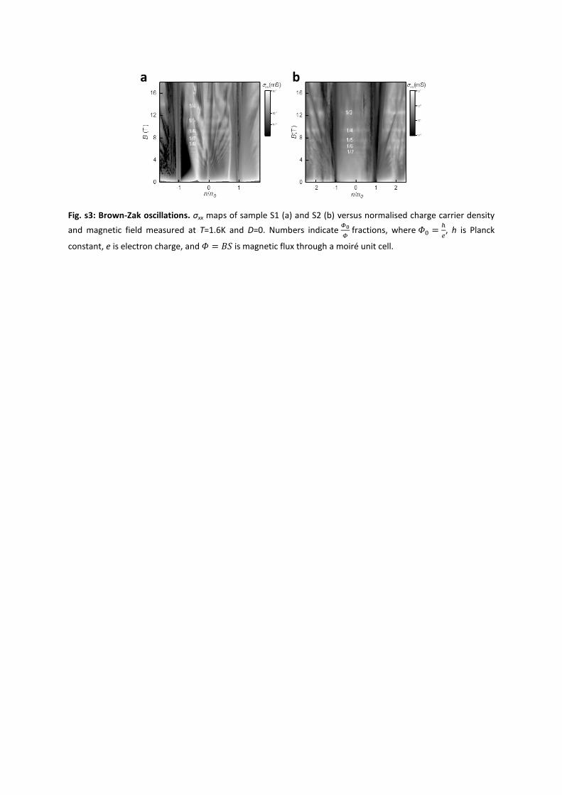
Fig. s3: Brown-Zak oscillations. σxx maps of sample S1 (a) and S2 (b) versus normalised charge carrier density
and magnetic field measured at T=1.6K and D=0. Numbers indicate 𝛷0
𝛷 fractions, where 𝛷0 =
ℎ
𝑒, h is Planck
constant, e is electron charge, and 𝛷 = 𝐵𝑆 is magnetic flux through a moiré unit cell.

Fig. s4: Dirac energy shift in the asymmetric evolution of band structure in tTLG. Energy units are in meV and
the path in k-space is ( 𝛤 ⟶ 𝐾/𝐾′ ⟶ 𝛤 ). (a) Band structure without coupling the two subsystems through the
tunnelling matrices T. (b) Band structure with non-zero tunnelling matrices for zero interlayer potential energy
difference U=0. The coupling of the two subsystems even without applying potential difference U results in
shifting the Dirac cone upwards. (c-h) Effect of applying positive interlayer potential energy difference U>0.
The bandgap at CNP needs U smaller than 30 meV to open. Moreover, electron band c1 is flatter than the hole
band v1. (i-n) Effect of applying negative interlayer potential energy difference U<0. In contrast to when U>0, it
requires larger energy difference U< -50 meV to open a gap at CNP.
Fig. s5: Dirac energy shift as a function of twist angle. Solid black curve is the Dirac energy shift produced by
our continuum model and the red dots are the results of tight-binding model in Ref 20.


