Download - UHF ASK/FSK Receiver ATA5724 ATA5728
Features• Frequency Receiving Range of (3 Versions)
– f0 = 312.5 MHz to 317.5 MHz or– f0 = 431.5 MHz to 436.5 MHz or– f0 = 868 MHz to 870 MHz
• 30 dB Image Rejection• Receiving Bandwidth
– BIF = 300 kHz for 315 MHz/433 MHz Version– BIF = 600 kHz for 868 MHz Version
• Fully Integrated LC-VCO and PLL Loop Filter• Very High Sensitivity with Power Matched LNA
– ATA5723/ATA5724:–107 dBm, FSK, BR_0 (1.0 kBit/s to 1.8 kBit/s), Manchester, BER 10E-3–113 dBm, ASK, BR_0 (1.0 kBit/s to 1.8 kBit/s), Manchester, BER 10E-3
– ATA5728:–105 dBm, FSK, BR_0 (1.0 kBit/s to 1.8 kBit/s), Manchester, BER 10E-3–111 dBm, ASK, BR_0 (1.0 kBit/s to 1.8 kBit/s), Manchester, BER 10E-3
• High System IIP3– –18 dBm at 868 MHz– –23 dBm at 433 MHz– –24 dBm at 315 MHz
• System 1-dB Compression Point – –27.7 dBm at 868 MHz– –32.7 dBm at 433 MHz– –33.7 dBm at 315 MHz
• High Large-signal Capability at GSM Band (Blocking –33 dBm at +10 MHz, IIP3 = –24 dBm at +20 MHz)
• Logarithmic RSSI Output• XTO Start-up with Negative Resistor of 1.5 kΩ• 5V to 20V Automotive Compatible Data Interface• Data Clock Available for Manchester and Bi-phase-coded Signals• Programmable Digital Noise Suppression• Low Power Consumption Due to Configurable Polling• Temperature Range –40°C to +105°C • ESD Protection 2 kV HBM, All Pins• Communication to Microcontroller Possible using a Single Bi-directional Data Line• Low-cost Solution Due to High Integration Level with Minimum External Circuitry
Requirements• Supply Voltage Range 4.5V to 5.5V
Benefits• Low BOM List Due to High Integration• Use of Low-cost 13 MHz Crystal• Lowest Average Current Consumption for Application Due to Self Polling Feature• Reuse of ATA5743 Software• World-wide Coverage with One PCB Due to 3 Versions are Pin Compatible
UHF ASK/FSK Receiver
ATA5723ATA5724ATA5728
9106E–RKE–07/08
29106E–RKE–07/08
ATA5723/ATA5724/ATA5728
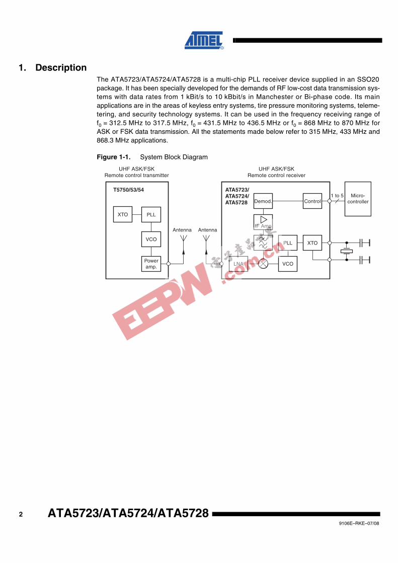
1. DescriptionThe ATA5723/ATA5724/ATA5728 is a multi-chip PLL receiver device supplied in an SSO20package. It has been specially developed for the demands of RF low-cost data transmission sys-tems with data rates from 1 kBit/s to 10 kBbit/s in Manchester or Bi-phase code. Its mainapplications are in the areas of keyless entry systems, tire pressure monitoring systems, teleme-tering, and security technology systems. It can be used in the frequency receiving range off0 = 312.5 MHz to 317.5 MHz, f0 = 431.5 MHz to 436.5 MHz or f0 = 868 MHz to 870 MHz forASK or FSK data transmission. All the statements made below refer to 315 MHz, 433 MHz and868.3 MHz applications.
Figure 1-1. System Block Diagram
Micro-controller
PLL
UHF ASK/FSKRemote control receiver
UHF ASK/FSKRemote control transmitter
T5750/53/54 ATA5723/ATA5724/ATA5728
LNA VCO
PLL XTO
Poweramp.
VCO
Antenna
Demod.
IF Amp
Control1 to 5
XTO
Antenna
39106E–RKE–07/08
ATA5723/ATA5724/ATA5728
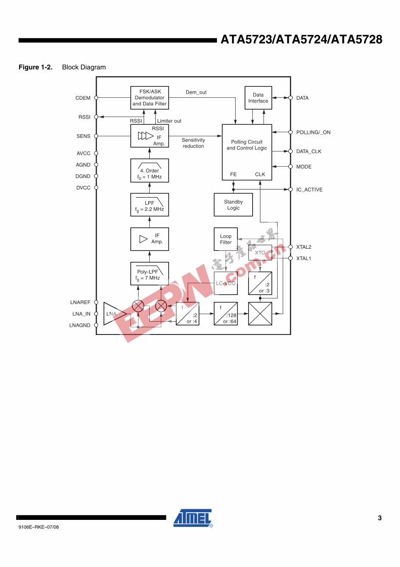
Figure 1-2. Block Diagram
4. Orderf0 = 1 MHz
IFAmp.
f
:2or :4
f
:2or :3
Polling Circuitand Control Logic
StandbyLogic
DataInterface
Sensitivityreduction
LoopFilter
f
:128or :64
IFAmp.
FSK/ASKDemodulator
and Data Filter
RSSI Limiter out
Dem_out
XTO
LNA
CLK
POLLING/_ON
IC_ACTIVE
XTAL1
XTAL2
MODE
DATA_CLK
DATA
FE
RSSI
Poly-LPFfg = 7 MHz
LPFfg = 2.2 MHz
CDEM
LNAREF
LNAGND
LNA_IN
DVCC
DGND
AGND
AVCC
SENS
RSSI
LC-VCO
49106E–RKE–07/08
ATA5723/ATA5724/ATA5728
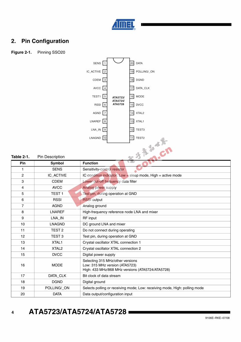
2. Pin Configuration
Figure 2-1. Pinning SSO20
TEST1
RSSI
LNA_IN
LNAGND
AGND
LNAREF
SENS
IC_ACTIVE
CDEM
AVCC
ATA5723/ATA5724/ATA5728
5
6
9
10
7
8
1
2
3
4
MODE
DVCC
TEST3
TEST2
XTAL2
XTAL1
DATA
POLLING/_ON
DGND
DATA_CLK
16
15
12
11
14
13
20
19
18
17
Table 2-1. Pin Description
Pin Symbol Function
1 SENS Sensitivity-control resistor
2 IC_ACTIVE IC condition indicator: Low = sleep mode, High = active mode
3 CDEM Lower cut-off frequency data filter
4 AVCC Analog power supply
5 TEST 1 Test pin, during operation at GND
6 RSSI RSSI output
7 AGND Analog ground
8 LNAREF High-frequency reference node LNA and mixer
9 LNA_IN RF input
10 LNAGND DC ground LNA and mixer
11 TEST 2 Do not connect during operating
12 TEST 3 Test pin, during operation at GND
13 XTAL1 Crystal oscillator XTAL connection 1
14 XTAL2 Crystal oscillator XTAL connection 2
15 DVCC Digital power supply
16 MODESelecting 315 MHz/other versionsLow: 315 MHz version (ATA5723)High: 433 MHz/868 MHz versions (ATA5724/ATA5728)
17 DATA_CLK Bit clock of data stream
18 DGND Digital ground
19 POLLING/_ON Selects polling or receiving mode; Low: receiving mode, High: polling mode
20 DATA Data output/configuration input

59106E–RKE–07/08
ATA5723/ATA5724/ATA5728
3. RF Front-endThe RF front-end of the receiver is a low-IF heterodyne configuration that converts the input sig-nal into about 1 MHz IF signal with a typical image rejection of 30 dB. According to Figure Figure1-2 on page 3 the front-end consists of an LNA (Low Noise Amplifier), LO (Local Oscillator), I/Qmixer, polyphase low-pass filter and an IF amplifier.
The PLL generates the drive frequency fLO for the mixer using a fully integrated synthesizer withintegrated low noise LC-VCO (Voltage Controlled Oscillator) and PLL-loop filter. The XTO (crys-tal oscillator) generates the reference frequency fREF = fXTO/2 (868 MHz and 433 MHz versions)or fREF = fXTO/3 (315 MHz version). The integrated LC-VCO generates two or four times themixer drive frequency fVCO. The I/Q signals for the mixer are generated with a divide by two orfour circuit (fLO = fVCO/2 for 868 MHz version, fLO = fVCO/4 for 433 MHz and 315 MHz versions).fVCO is divided by a factor of 128 or 64 and feeds into a phase frequency detector and is com-pared with fREF. The output of the phase frequency detector is fed into an integrated loop filterand thereby generates the control voltage for the VCO. If fLO is determined, fXTO can be calcu-lated using the following formula:
fREF = fLO/128 for 868 MHz band, fREF = fLO/64 for 433 MHz bands, fREF = fLO/64 for 315 MHzbands.
The XTO is a two-pin oscillator that operates at the series resonance of the quartz crystal withhigh current but low voltage signal, so that there is only a small voltage at the crystal oscillatorfrequency at pins XTAL1 and XTAL2. According to Figure 3-1, the crystal should be connectedto GND with two capacitors CL1 and CL2 from XTAL1 and XTAL2 respectively. The value ofthese capacitors are recommended by the crystal supplier. Due to an inductive impedance atsteady state oscillation and some PCB parasitics, a lower value of CL1 and CL2 is normallynecessary.
The value of CLx should be optimized for the individual board layout to achieve the exact value offXTO and hence of fLO. (The best way is to use a crystal with known load resonance frequency tofind the right value for this capacitor.) When designing the system in terms of receiving band-width and local oscillator accuracy, the accuracy of the crystal and the XTO must be considered.
Figure 3-1. XTO Peripherals
The nominal frequency fLO is determined by the RF input frequency fRF and the IF frequency fIFusing the following formula (low-side injection):
fLO = fRF – fIF
XTAL2
TEST2
TEST3
XTAL1
DVCCVS
CL2
CL1

69106E–RKE–07/08
ATA5723/ATA5724/ATA5728
To determine fLO, the construction of the IF filter must be considered. The nominal IF frequencyis fIF = 950 kHz. To achieve a good accuracy of the filter corner frequencies, the filter is tuned bythe crystal frequency fXTO. This means that there is a fixed relationship between fIF and fLO.
fIF = fLO/318 for the 315 MHz band (ATA5723)fIF = fLO/438 for the 433.92 MHz band (ATA5724)fIF = fLO/915 for the 868.3 MHz band (ATA5728)
The relationship is designed to achieve the nominal IF frequency of:
fIF = 987 kHz for the 315 MHz and BIF = 300 kHz (ATA5723)fIF = 987 kHz for the 433.92 MHz and BIF = 300 kHz (ATA5724)fIF = 947.8 kHz for the 868.3 MHz and BIF = 600 kHz (ATA5728)
The RF input either from an antenna or from an RF generator must be transformed to the RFinput pin LNA_IN. The input impedance of this pin is provided in the electrical parameters. Theparasitic board inductances and capacitances influence the input matching. The RF receiverATA5723/ATA5724/ATA5728 exhibits its highest sensitivity if the LNA is power matched.Because of this, matching to a SAW filter, a 50Ω or an antenna is easier.
Figure 14-1 on page 32 “Application Circuit” shows a typical input matching network forfRF = 315 MHz, fRF = 433.92 MHz or fRF = 868.3 MHz to 50Ω. The input matching network shownin Table 14-2 on page 32 is the reference network for the parameters given in the electricalcharacteristics.
4. Analog Signal Processing
4.1 IF FilterThe signals coming from the RF front-end are filtered by the fully integrated 4th-order IF filter.The IF center frequency is:
fIF = 987 kHz for the 315 MHz and BIF = 300 kHz (ATA5723)fIF = 987 kHz for the 433.92 MHz and BIF = 300 kHz (ATA5724)fIF = 947.9 kHz for the 868.3 MHz and BIF = 600 kHz (ATA5728)
The nominal bandwidth is 300 kHz for ATA5723 and ATA5724 and 600 kHz for ATA5728.
4.2 Limiting RSSI AmplifierThe subsequent RSSI amplifier enhances the output signal of the IF amplifier before it is fed intothe demodulator. The dynamic range of this amplifier is ΔRRSSI = 60 dB. If the RSSI amplifier isoperated within its linear range, the best S/N ratio is maintained in ASK mode. If the dynamicrange is exceeded by the transmitter signal, the S/N ratio is defined by the ratio of the maximumRSSI output voltage and the RSSI output voltage due to a disturber. The dynamic range of theRSSI amplifier is exceeded if the RF input signal is approximately 60 dB higher compared to theRF input signal at full sensitivity.
The S/N ratio is not affected by the dynamic range of the RSSI amplifier in FSK mode becauseonly the hard limited signal from a high-gain limiting amplifier is used by the demodulator.
The output voltage of the RSSI amplifier (VRSSI) is available at pin RSSI. Using the RSSI outputsignal, the signal strength of different transmitters can be distinguished. The usable input powerrange PRef is –100 dBm to –55 dBm.
79106E–RKE–07/08
ATA5723/ATA5724/ATA5728
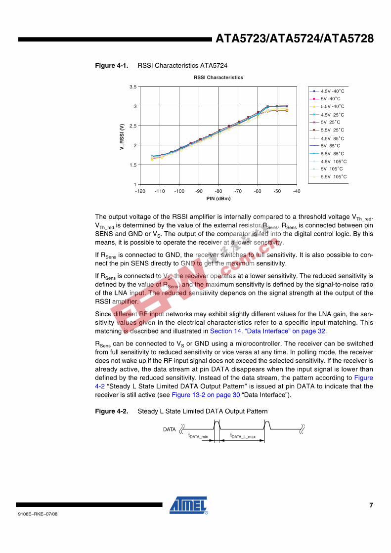
Figure 4-1. RSSI Characteristics ATA5724
The output voltage of the RSSI amplifier is internally compared to a threshold voltage VTh_red.VTh_red is determined by the value of the external resistor RSens. RSens is connected between pinSENS and GND or VS. The output of the comparator is fed into the digital control logic. By thismeans, it is possible to operate the receiver at a lower sensitivity.
If RSens is connected to GND, the receiver switches to full sensitivity. It is also possible to con-nect the pin SENS directly to GND to get the maximum sensitivity.
If RSens is connected to VS, the receiver operates at a lower sensitivity. The reduced sensitivity isdefined by the value of RSens, and the maximum sensitivity is defined by the signal-to-noise ratioof the LNA input. The reduced sensitivity depends on the signal strength at the output of theRSSI amplifier.
Since different RF input networks may exhibit slightly different values for the LNA gain, the sen-sitivity values given in the electrical characteristics refer to a specific input matching. Thismatching is described and illustrated in Section 14. “Data Interface” on page 32.
RSens can be connected to VS or GND using a microcontroller. The receiver can be switchedfrom full sensitivity to reduced sensitivity or vice versa at any time. In polling mode, the receiverdoes not wake up if the RF input signal does not exceed the selected sensitivity. If the receiver isalready active, the data stream at pin DATA disappears when the input signal is lower thandefined by the reduced sensitivity. Instead of the data stream, the pattern according to Figure4-2 “Steady L State Limited DATA Output Pattern” is issued at pin DATA to indicate that thereceiver is still active (see Figure 13-2 on page 30 “Data Interface”).
Figure 4-2. Steady L State Limited DATA Output Pattern
5.5V -40˚C
4.5V -40˚C
5V 25˚C
5.5V 25˚C
5V 105˚C
5.5V 105˚C
4.5V 105˚C
4.5V 85˚C
5.5V 85˚C
5V 85˚C
4.5V 25˚C
5V -40˚C
3.5
3
2.5
2
1.5
-120 -110 -100 -90
PIN (dBm)
V_R
SS
I (V
)
RSSI Characteristics
-80 -70 -60 -50 -401
tDATA_L_maxtDATA_min
DATA

89106E–RKE–07/08
ATA5723/ATA5724/ATA5728
4.3 FSK/ASK Demodulator and Data FilterThe signal coming from the RSSI amplifier is converted into the raw data signal by the ASK/FSKdemodulator. The operating mode of the demodulator is set using the bit ASK/_FSK in theOPMODE register. Logic L sets the demodulator to FSK, applying H to ASK mode.
In ASK mode an automatic threshold control circuit (ATC) is employed to set the detection refer-ence voltage to a value where a good signal to noise ratio is achieved. This circuit alsoimplements the effective suppression of any kind of in-band noise signals or competing transmit-ters. If the S/N (ratio to suppress in-band noise signals) exceeds about 10 dB the data signal canbe detected properly. However, better values are found for many modulation schemes of thecompeting transmitter.
The FSK demodulator is intended to be used for an FSK deviation of 10 kHz ≤Δf ≤100 kHz. Thedata signal in FSK mode can be detected if the S/N (ratio to suppress in-band noise signals)exceeds about 2 dB. This value is valid for all modulation schemes of a disturber signal.
The output signal of the demodulator is filtered by the data filter before it is fed into the digitalsignal processing circuit. The data filter improves the S/N ratio as its pass-band can be adoptedto the characteristics of the data signal. The data filter consists of a 1st order high-pass and a 2nd
order low-pass filter.
The high-pass filter cut-off frequency is defined by an external capacitor connected to pinCDEM. The cut-off frequency of the high-pass filter is defined by the following formula:
In self-polling mode the data filter must settle very rapidly to achieve a low current consumption.Therefore, CDEM cannot be increased to very high values if self-polling is used. On the otherhand, CDEM must be large enough to meet the data filter requirements according to the datasignal. Recommended values for CDEM are given in the electrical characteristics.
The cut-off frequency of the low-pass filter is defined by the selected baud-rate range(BR_Range). The BR_Range is defined in the OPMODE register (refer to Section 11. “Configur-ing the Receiver” on page 25). The BR_Range must be set in accordance to the baud-rate used.
The ATA5723/ATA5724/ATA5728 is designed to operate with data coding where the DC level ofthe data signal is 50%. This is valid for Manchester and Bi-phase coding. If other modulationschemes are used, the DC level should always remain within the range of VDC_min = 33% andVDC_max = 66%. The sensitivity may be reduced by up to 2 dB in that condition.
Each BR_Range is also defined by a minimum and a maximum edge-to-edge time (tee_sig).These limits are defined in the electrical characteristics. They should not be exceeded to main-tain full sensitivity of the receiver.
fcu_DF 12 π× 30 kΩ× CDEM×-------------------------------------------------------------=

99106E–RKE–07/08
ATA5723/ATA5724/ATA5728
5. Receiving CharacteristicsThe RF receiver ATA5723/ATA5724/ATA5728 can be operated with and without a SAWfront-end filter. In a typical automotive application, a SAW filter is used to achieve better selectiv-ity and large signal capability. The receiving frequency response without a SAW front-end filter isillustrated in Figure 5-1 “Narrow Band Receiving Frequency Response ATA5724”. This examplerelates to ASK mode. FSK mode exhibits a similar behavior. The plots are printed relatively tothe maximum sensitivity. If a SAW filter is used, an insertion loss of about 3 dB must be consid-ered, but the overall selectivity is much better.
When designing the system in terms of receiving bandwidth, the LO deviation must be consid-ered as it also determines the IF center frequency. The total LO deviation is calculated, to be thesum of the deviation of the crystal and the XTO deviation of the ATA5723/ATA5724/ATA5728.Low-cost crystals are specified to be within ±90 ppm over tolerance, temperature, and aging.The XTO deviation of the ATA5723/ATA5724/ATA5728 is an additional deviation due to theXTO circuit. This deviation is specified to be ±10 ppm worst case for a crystal with CM = 7 fF. Ifa crystal of ±90 ppm is used, the total deviation is ±100 ppm in that case. Note that the receivingbandwidth and the IF-filter bandwidth are equivalent in ASK mode but not in FSK mode.
Figure 5-1. Narrow Band Receiving Frequency Response ATA5724
10
0
-10
-20
-30
-40
-50
-60
-70
(dB
)
5.5V -40˚C
4.5V -40˚C
5V 25˚C
5.5V 25˚C
4.5V 105˚C
5.5V 105˚C
5V 105˚C
4.5V 25˚C
5V -40˚C
430 431 432 433
(MHz)
Image Rejection versus RF Frequency
434 435 436 437 438
109106E–RKE–07/08
ATA5723/ATA5724/ATA5728
6. Polling Circuit and Control LogicThe receiver is designed to consume less than 1 mA while being sensitive to signals from a cor-responding transmitter. This is achieved using the polling circuit. This circuit enables the signalpath periodically for a short time. During this time the bit-check logic verifies the presence of avalid transmitter signal. Only if a valid signal is detected, the receiver remains active and trans-fers the data to the connected microcontroller. If there is no valid signal present, the receiver isin sleep mode most of the time resulting in low current consumption. This condition is called poll-ing mode. A connected microcontroller is disabled during that time.
All relevant parameters of the polling logic can be configured by the connected microcontroller.This flexibility enables the user to meet the specifications in terms of current consumption, sys-tem response time, data rate etc.
The receiver is very flexible with regards to the number of connection wires to the microcon-troller. It can be either operated by a single bi-directional line to save ports to the connectedmicrocontroller or it can be operated by up to five uni-directional ports.
7. Basic Clock Cycle of the Digital CircuitryThe complete timing of the digital circuitry and the analog filtering is derived from one clock. Thisclock cycle TClk is derived from the crystal oscillator (XTO) in combination with a divide by 28 or30 circuit. According to Section 3. “RF Front-end” on page 5, the frequency of the crystal oscilla-tor (fXTO) is defined by the RF input signal (fRFin) which also defines the operating frequency ofthe local oscillator (fLO). The basic clock cycle for ATA5724 and ATA5728 is TClk 28/fXTO givingTClk = 2.066 µs for fRF = 868.3 MHz and TClk = 2.069 µs for fRF = 433.92 MHz. For ATA5723 thebasic clock cycle is TClk = 30/fREF giving TClk = 2.0382 µs for fRF = 315 MHz.
TClk controls the following application-relevant parameters:
• Timing of the polling circuit including bit check
• Timing of the analog and digital signal processing
• Timing of the register programming
• Frequency of the reset marker
• IF filter center frequency (fIF0)
Most applications are dominated by three transmission frequencies: fTransmit = 315 MHz is mainlyused in USA, fTransmit = 868.3 MHz and 433.92 MHz in Europe. All timings are based on TClk. Forthe aforementioned frequencies, TClk is given as:
• Application 315 MHz band (fXTO = 14.71875 MHz, fLO = 314.13 MHz, TClk = 2.0382 µs)
• Application 868.3 MHz band (fXTO = 13.55234 MHz, fLO = 867.35 MHz, TClk = 2.066 µs)
• Application 433.92 MHz band (fXTO = 13.52875 MHz, fLO = 432.93 MHz, TClk = 2.0696 µs)
For calculation of TClk for applications using other frequency bands, see table in Section 18.“Electrical Characteristics ATA5724, ATA5728” on page 37.

119106E–RKE–07/08
ATA5723/ATA5724/ATA5728
The clock cycle of some function blocks depends on the selected baud-rate range (BR_Range),which is defined in the OPMODE register. This clock cycle TXClk is defined by the followingformulas:
BR_Range = BR_Range0: TXClk = 8 × TClk
BR_Range1: TXClk = 4 × TClk
BR_Range2: TXClk = 2 × TClk
BR_Range3: TXClk = 1 × TClk
8. Polling ModeAccording to Figure 8-1 on page 12, the receiver stays in polling mode in a continuous cycle ofthree different modes. In sleep mode the signal processing circuitry is disabled for the timeperiod TSleep while consuming low current of IS = ISoff. During the start-up period, TStartup, all sig-nal processing circuits are enabled and settled. In the following bit-check mode, the incomingdata stream is analyzed bit-by-bit and compared with a valid transmitter signal. If no valid signalis present, the receiver is set back to sleep mode after the period TBit-check. This period variesaccording to each check as it is a statistical process. An average value for TBitcheck is given in theelectrical characteristics. During TStartup and TBit-check, the current consumption is IS = ISon. Thecondition of the receiver is indicated on pin IC_ACTIVE. The average current consumption inpolling mode is dependent on the duty cycle of the active mode and can be calculated as:
During TSleep and TStartup, the receiver is not sensitive to a transmitter signal. To guarantee thereception of a transmitted command, the transmitter must start the telegram with an adequatepreburst. The required length of the preburst depends on the polling parameters TSleep, TStartup,TBit-check and the start-up time of a connected microcontroller, TStart_microcontroller. Thus, TBit-check
depends on the actual bit rate and the number of bits (NBit-check) to be tested.
The following formula indicates how to calculate the preburst length.
TPreburst ≥ TSleep + TStartup + TBit-check + TStart_microcontroller
8.1 Sleep ModeThe length of period TSleep is defined by the 5-bit word Sleep of the OPMODE register, the exten-sion factor XSleep (according to Table 11-8 on page 27), and the basic clock cycle TClk. It iscalculated to be:
TSleep = Sleep × XSleep × 1024 × TClk
The maximum value of TSleep is about 60 ms if XSleep is set to 1. The time resolution is about2 ms in that case. The sleep time can be extended to almost half a second by setting XSleep to 8.XSleep can be set to 8 by bit XSleepStd to “1”.
Setting the configuration word Sleep to its maximal value puts the receiver into a permanentsleep mode. The receiver remains in this state until another value for Sleep is programmed intothe OPMODE register. This is particularily useful when several devices share a single data line.(It can also be used for microcontroller polling: using pin POLLING/_ON, the receiver can beswitched on and off.)
ISpollISoff TSleep ISon TStartup TBit-check+( )×+×
TSleep TStartup TBit-check+ +----------------------------------------------------------------------------------------------------------------=

129106E–RKE–07/08
ATA5723/ATA5724/ATA5728
Figure 8-1. Polling Mode Flow Chart
Bit-check Mode:The incoming data stream isanalyzed. If the timing indicates a validtransmitter signal, the receiver is set toreceiving mode. Otherwise it is set toSleep mode.Output level on Pin IC_ACTIVE = > high
TBit-check
IS = ISon
Start-up Mode:The signal processing circuits areenabled. After the start-up time (TStartup)all circuits are in stablecondition and ready to receive.Output level on Pin IC_ACTIVE = > high
TStartup
IS = ISon
Receiving Mode:The receiver is turned on permanentlyand passes the data stream to theconnected microcontroller.It can be set to Sleep mode through anOFF command via Pin DATA orPolling/_ON.Output level on Pin IC_ACTIVE = > highIS = ISon
Sleep Mode:All circuits for signal processing aredisabled. Only XTO and Polling logic areenabled.Output level on Pin IC_ACTIVE = > low
TSleep = Sleep × XSleep × 1024 × TClk
IS = ISoff
Bit CheckOK ?
5-bit word defined by Sleep 0 toSleep 4 in OPMODE register
Sleep:
Is defined by the selected baud raterange and TClk. The baud-rate rangeis defined by Baud 0 and Baud 1 inthe OPMODE register.
TStartup:
Basic clock cycle defined by fXTOand Pin MODE
TClk:
If the bit check fails, the averagetime period for that check dependson the selected baud-rate range andon TClk. The baud-rate range isdefined by Baud 0 and Baud 1 in theOPMODE register.
If the bit check is ok, TBit-checkdepends on the number of bits to bechecked (NBit-check) and on thedata rate used.
Depends on the result of the bit checkTBit-check:
Extension factor defined byXSleepStd according to Table 11-8
XSleep:
OFF Command
YES
NO
139106E–RKE–07/08
ATA5723/ATA5724/ATA5728
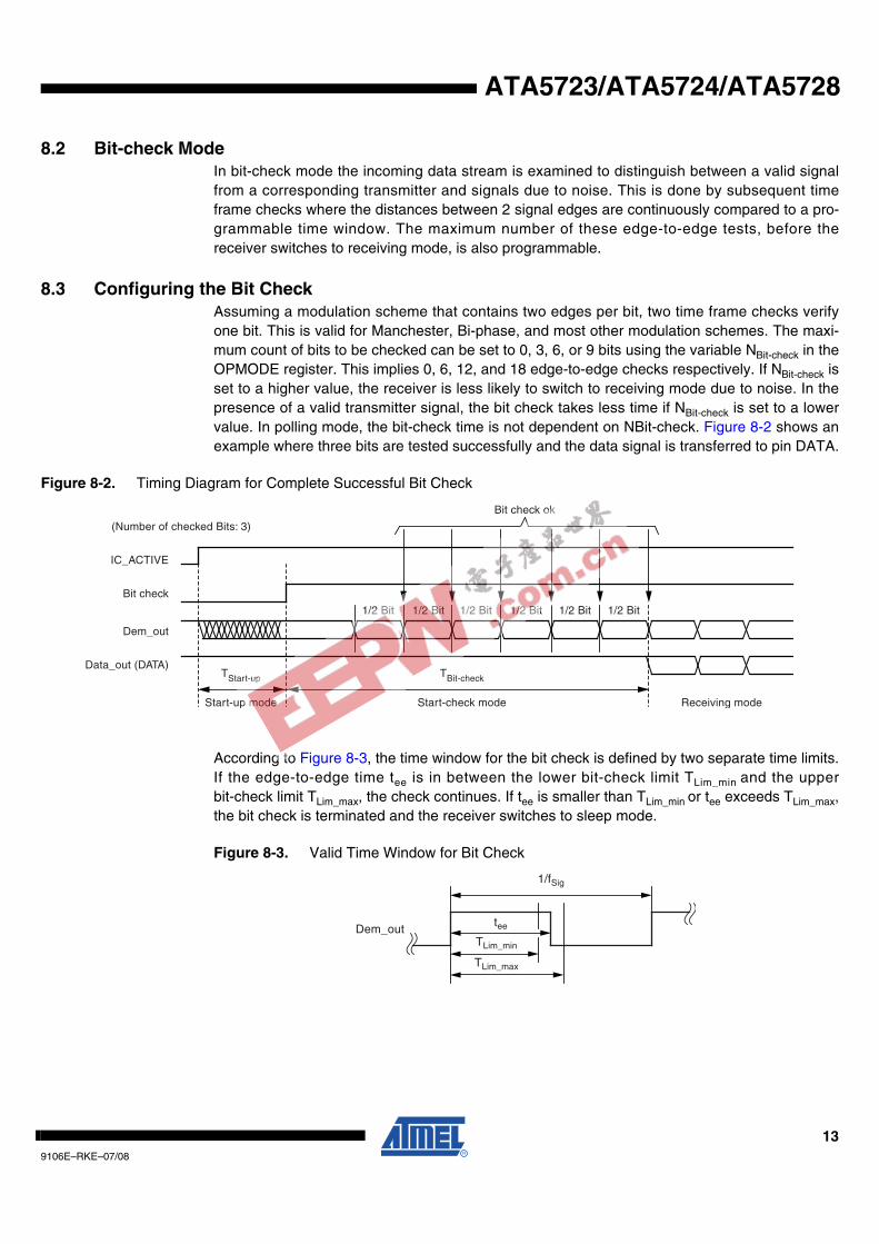
8.2 Bit-check ModeIn bit-check mode the incoming data stream is examined to distinguish between a valid signalfrom a corresponding transmitter and signals due to noise. This is done by subsequent timeframe checks where the distances between 2 signal edges are continuously compared to a pro-grammable time window. The maximum number of these edge-to-edge tests, before thereceiver switches to receiving mode, is also programmable.
8.3 Configuring the Bit CheckAssuming a modulation scheme that contains two edges per bit, two time frame checks verifyone bit. This is valid for Manchester, Bi-phase, and most other modulation schemes. The maxi-mum count of bits to be checked can be set to 0, 3, 6, or 9 bits using the variable NBit-check in theOPMODE register. This implies 0, 6, 12, and 18 edge-to-edge checks respectively. If NBit-check isset to a higher value, the receiver is less likely to switch to receiving mode due to noise. In thepresence of a valid transmitter signal, the bit check takes less time if NBit-check is set to a lowervalue. In polling mode, the bit-check time is not dependent on NBit-check. Figure 8-2 shows anexample where three bits are tested successfully and the data signal is transferred to pin DATA.
Figure 8-2. Timing Diagram for Complete Successful Bit Check
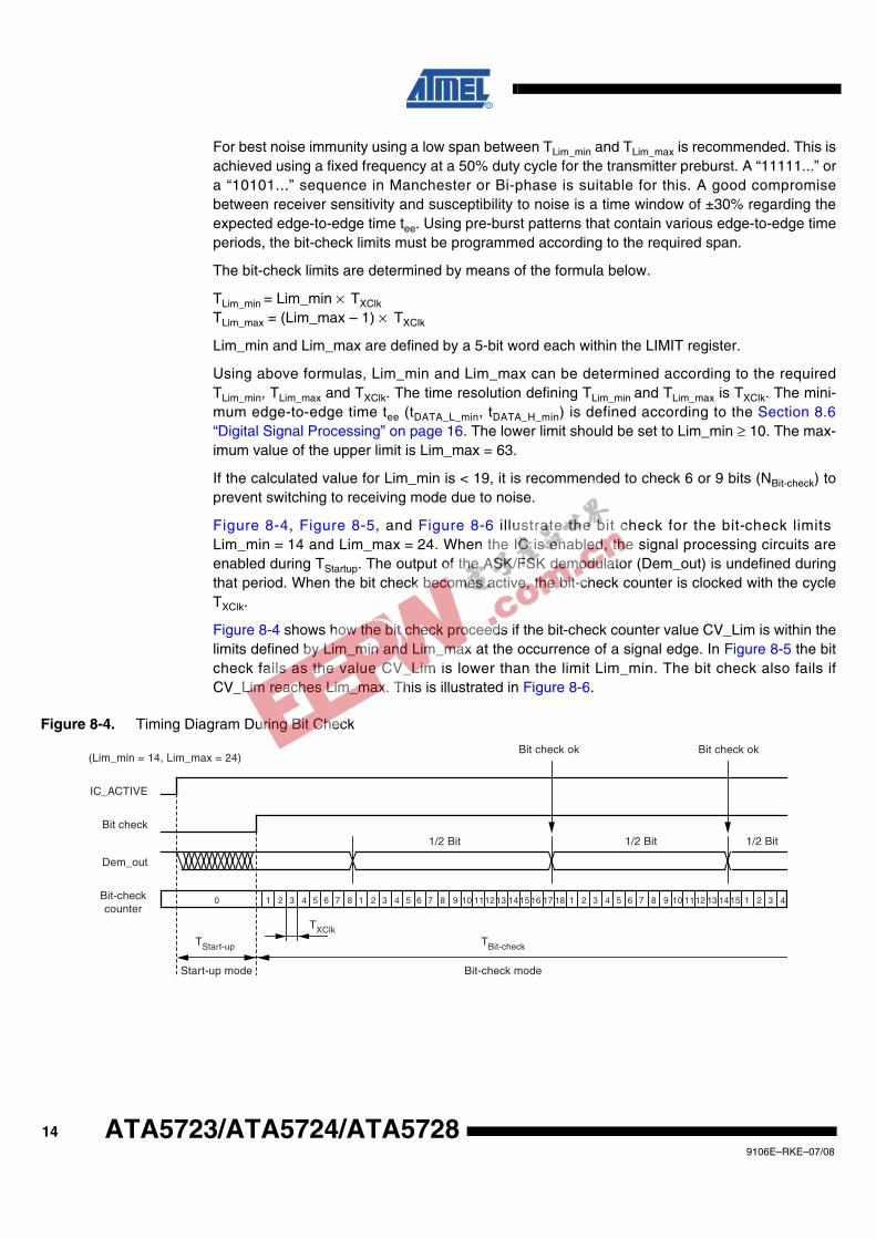
According to Figure 8-3, the time window for the bit check is defined by two separate time limits.If the edge-to-edge time tee is in between the lower bit-check limit TLim_min and the upperbit-check limit TLim_max, the check continues. If tee is smaller than TLim_min or tee exceeds TLim_max,the bit check is terminated and the receiver switches to sleep mode.
Figure 8-3. Valid Time Window for Bit Check
IC_ACTIVE
Data_out (DATA)
Dem_out
Bit check
TBit-check
Start-up mode
(Number of checked Bits: 3)
Bit check ok
1/2 Bit 1/2 Bit 1/2 Bit1/2 Bit1/2 Bit1/2 Bit
Start-check mode Receiving mode
TStart-up
1/fSig
tee
TLim_max
TLim_min
Dem_out
149106E–RKE–07/08
ATA5723/ATA5724/ATA5728
For best noise immunity using a low span between TLim_min and TLim_max is recommended. This isachieved using a fixed frequency at a 50% duty cycle for the transmitter preburst. A “11111...” ora “10101...” sequence in Manchester or Bi-phase is suitable for this. A good compromisebetween receiver sensitivity and susceptibility to noise is a time window of ±30% regarding theexpected edge-to-edge time tee. Using pre-burst patterns that contain various edge-to-edge timeperiods, the bit-check limits must be programmed according to the required span.
The bit-check limits are determined by means of the formula below.
TLim_min = Lim_min × TXClk
TLim_max = (Lim_max – 1) × TXClk
Lim_min and Lim_max are defined by a 5-bit word each within the LIMIT register.
Using above formulas, Lim_min and Lim_max can be determined according to the requiredTLim_min, TLim_max and TXClk. The time resolution defining TLim_min and TLim_max is TXClk. The mini-mum edge-to-edge time tee (tDATA_L_min, tDATA_H_min) is defined according to the Section 8.6“Digital Signal Processing” on page 16. The lower limit should be set to Lim_min ≥ 10. The max-imum value of the upper limit is Lim_max = 63.
If the calculated value for Lim_min is < 19, it is recommended to check 6 or 9 bits (NBit-check) toprevent switching to receiving mode due to noise.
Figure 8-4, Figure 8-5, and Figure 8-6 illustrate the bit check for the bit-check limitsLim_min = 14 and Lim_max = 24. When the IC is enabled, the signal processing circuits areenabled during TStartup. The output of the ASK/FSK demodulator (Dem_out) is undefined duringthat period. When the bit check becomes active, the bit-check counter is clocked with the cycleTXClk.
Figure 8-4 shows how the bit check proceeds if the bit-check counter value CV_Lim is within thelimits defined by Lim_min and Lim_max at the occurrence of a signal edge. In Figure 8-5 the bitcheck fails as the value CV_Lim is lower than the limit Lim_min. The bit check also fails ifCV_Lim reaches Lim_max. This is illustrated in Figure 8-6.
Figure 8-4. Timing Diagram During Bit Check
IC_ACTIVE
Bit-checkcounter
Dem_out
Bit check
TBit-check
Start-up mode
(Lim_min = 14, Lim_max = 24)Bit check okBit check ok
7 85 6 3 41 23 4 1513 1411129 101 27 85 63 4 17 1815 1613 1411129 101 27 85 63 41 20
1/2 Bit 1/2 Bit1/2 Bit
Bit-check mode
TStart-up
TXClk

159106E–RKE–07/08
ATA5723/ATA5724/ATA5728
Figure 8-5. Timing Diagram for Failed Bit Check (Condition: CV_Lim < Lim_min)
Figure 8-6. Timing Diagram for Failed Bit Check (Condition: CV_Lim ≥ Lim_max)
8.4 Duration of the Bit CheckIf no transmitter signal is present during the bit check, the output of the ASK/FSK demodulatordelivers random signals. The bit check is a statistical process and TBit-check varies for each check.Therefore, an average value for TBit-check is given in the electrical characteristics. TBit-check
depends on the selected baud-rate range and on TClk. A higher baud-rate range causes a lowervalue for TBit-check resulting in a lower current consumption in polling mode.
In the presence of a valid transmitter signal, TBit-check is dependent on the frequency of that sig-nal, fSig, and the count of the checked bits, NBit-check. A higher value for NBit-check thereby results ina longer period for TBit-check requiring a higher value for the transmitter pre-burst TPreburst.
8.5 Receiving ModeIf the bit check was successful for all bits specified by NBit-check, the receiver switches to receivingmode. According to Figure 8-2 on page 13, the internal data signal is switched to pin DATA inthat case, and the data clock is available after the start bit has been detected (see Figure 9-1 onpage 20). A connected microcontroller can be woken up by the negative edge at pin DATA or bythe data clock at pin DATA_CLK. The receiver stays in that condition until it is switched back topolling mode explicitly.
IC_ACTIVE
Bit-checkcounter
Dem_out
Bit check
TBit-check
Sleep mode
0
TSleep
Start-up mode
(Lim_min = 14, Lim_max = 24) Bit check failed (CV_Lim_ < Lim_min)
86 74 5 11129 102 315 63 41 20
1/2 Bit
Bit-check mode
TStart-up
IC_ACTIVE
Bit-checkcounter
Dem_out
Bit check
TBit-check
Sleep mode
0
TSleep
Start-up mode
(Lim_min = 14, Lim_max = 24) Bit check failed (CV_Lim ≥ Lim_max)
23 2421 2219 2086 74 5 17 1815 1613 1411129 102 37 15 63 41 20
1/2 Bit
Bit-check mode
TStart-up
169106E–RKE–07/08
ATA5723/ATA5724/ATA5728
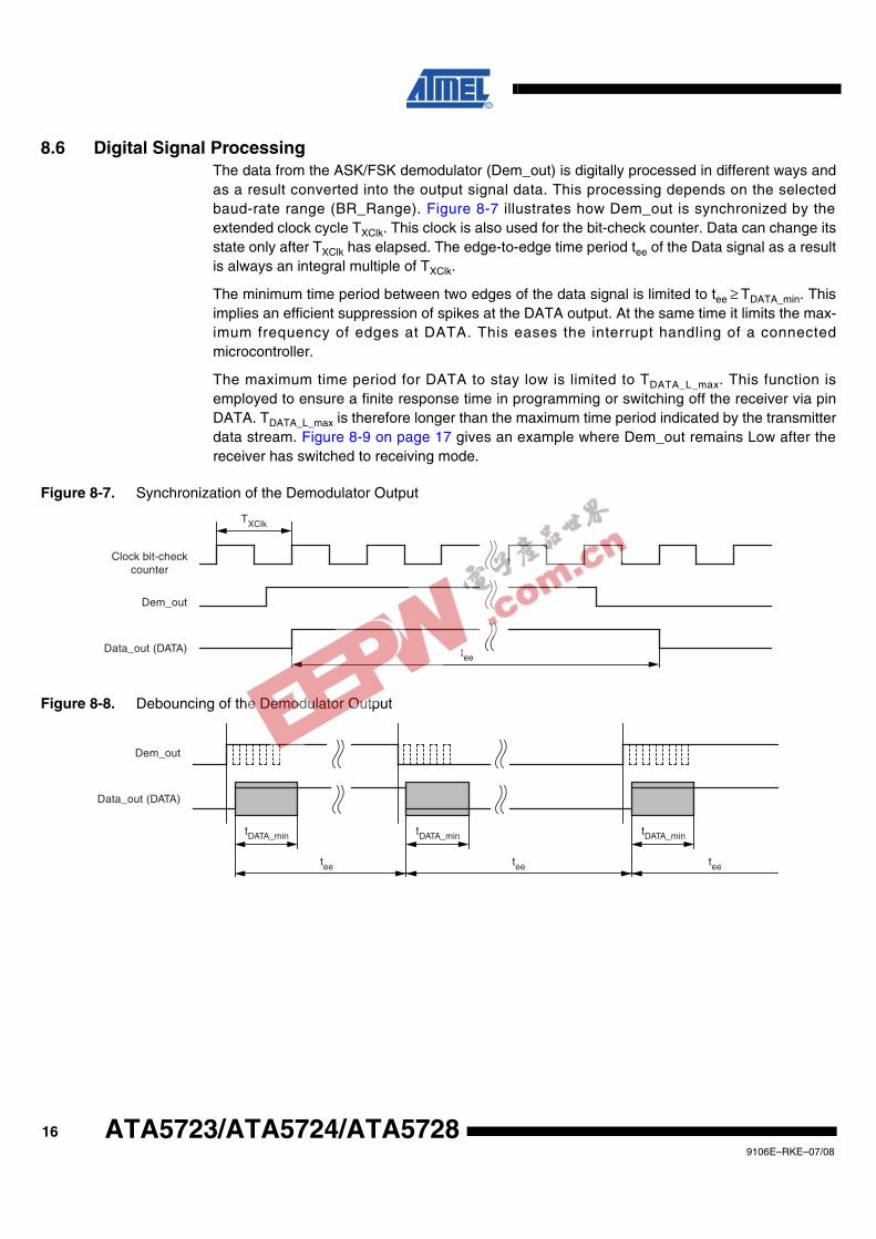
8.6 Digital Signal ProcessingThe data from the ASK/FSK demodulator (Dem_out) is digitally processed in different ways andas a result converted into the output signal data. This processing depends on the selectedbaud-rate range (BR_Range). Figure 8-7 illustrates how Dem_out is synchronized by theextended clock cycle TXClk. This clock is also used for the bit-check counter. Data can change itsstate only after TXClk has elapsed. The edge-to-edge time period tee of the Data signal as a resultis always an integral multiple of TXClk.
The minimum time period between two edges of the data signal is limited to tee ≥ TDATA_min. Thisimplies an efficient suppression of spikes at the DATA output. At the same time it limits the max-imum frequency of edges at DATA. This eases the interrupt handling of a connectedmicrocontroller.
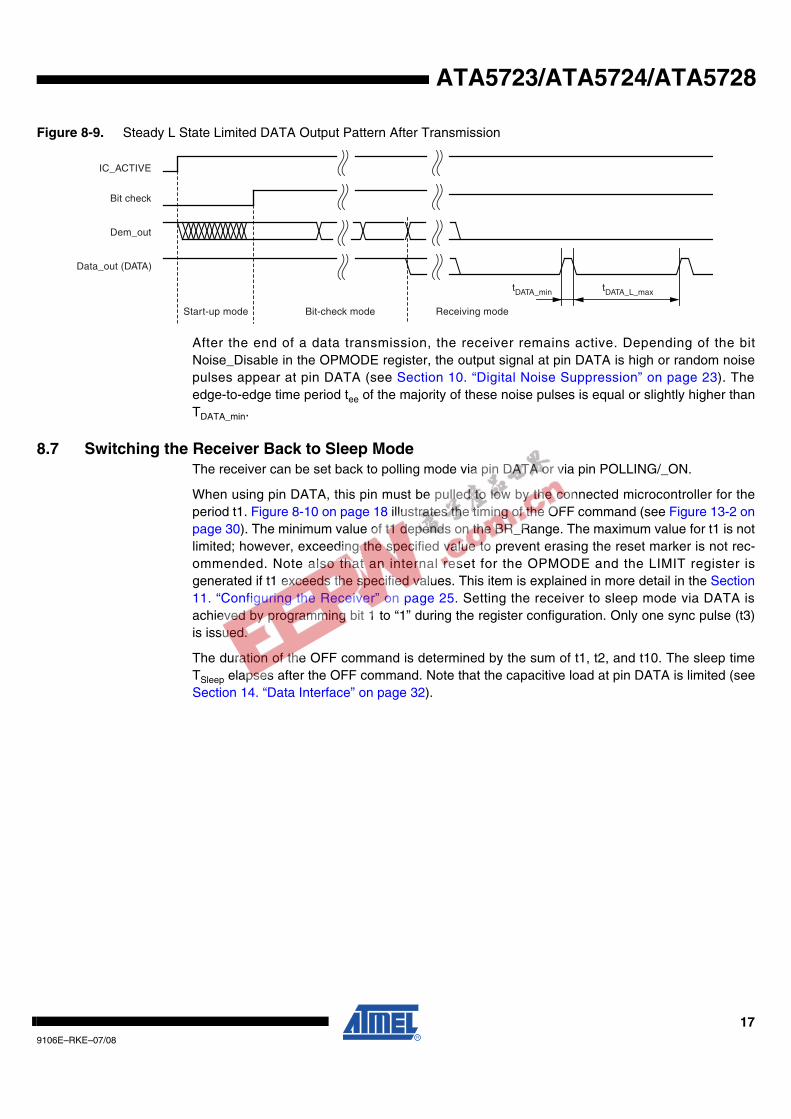
The maximum time period for DATA to stay low is limited to TDATA_L_max. This function isemployed to ensure a finite response time in programming or switching off the receiver via pinDATA. TDATA_L_max is therefore longer than the maximum time period indicated by the transmitterdata stream. Figure 8-9 on page 17 gives an example where Dem_out remains Low after thereceiver has switched to receiving mode.
Figure 8-7. Synchronization of the Demodulator Output
Figure 8-8. Debouncing of the Demodulator Output
Data_out (DATA)
Clock bit-checkcounter
Dem_out
TXClk
tee
Data_out (DATA)
Dem_out
teeteetee
tDATA_min tDATA_min tDATA_min
179106E–RKE–07/08
ATA5723/ATA5724/ATA5728
Figure 8-9. Steady L State Limited DATA Output Pattern After Transmission
After the end of a data transmission, the receiver remains active. Depending of the bitNoise_Disable in the OPMODE register, the output signal at pin DATA is high or random noisepulses appear at pin DATA (see Section 10. “Digital Noise Suppression” on page 23). Theedge-to-edge time period tee of the majority of these noise pulses is equal or slightly higher thanTDATA_min.
8.7 Switching the Receiver Back to Sleep ModeThe receiver can be set back to polling mode via pin DATA or via pin POLLING/_ON.
When using pin DATA, this pin must be pulled to low by the connected microcontroller for theperiod t1. Figure 8-10 on page 18 illustrates the timing of the OFF command (see Figure 13-2 onpage 30). The minimum value of t1 depends on the BR_Range. The maximum value for t1 is notlimited; however, exceeding the specified value to prevent erasing the reset marker is not rec-ommended. Note also that an internal reset for the OPMODE and the LIMIT register isgenerated if t1 exceeds the specified values. This item is explained in more detail in the Section11. “Configuring the Receiver” on page 25. Setting the receiver to sleep mode via DATA isachieved by programming bit 1 to “1” during the register configuration. Only one sync pulse (t3)is issued.
The duration of the OFF command is determined by the sum of t1, t2, and t10. The sleep timeTSleep elapses after the OFF command. Note that the capacitive load at pin DATA is limited (seeSection 14. “Data Interface” on page 32).
IC_ACTIVE
Data_out (DATA)
Dem_out
Bit check
tDATA_L_maxtDATA_min
Receiving modeStart-up mode Bit-check mode

189106E–RKE–07/08
ATA5723/ATA5724/ATA5728
Figure 8-10. Timing Diagram of the OFF Command using Pin DATA
Figure 8-11. Timing Diagram of the OFF Command using Pin POLLING/_ON
Figure 8-12. Activating the Receiving Mode using Pin POLLING/_ON
IC_ACTIVE
Serial bi-directionaldata line
Out1(microcontroller)
Data_out (DATA)
TSleep TStart-up
t7
t4
t5t3t2t1
t10
Bit 1("1")
(Start Bit)
OFF-command
X
X
Receiving mode Sleep mode Start-up mode
IC_ACTIVE
POLLING/_ON
Serial bi-directionaldata line
Data_out (DATA)
ton2 ton3
Receiving mode Sleep mode Start-up mode Receiving modeBit-check mode
Bit check ok
X X
X X
IC_ACTIVE
POLLING/_ON
Serial bi-directionaldata line
Data_out (DATA)
ton1
Start-up modeSleep mode Receiving mode
X
X

199106E–RKE–07/08
ATA5723/ATA5724/ATA5728
Figure 8-11 “Timing Diagram of the OFF Command using Pin POLLING/_ON” illustrates how toset the receiver back to polling mode using pin POLLING/_ON. The pin POLLING/_ON must beheld to low for the time period ton2. After the positive edge on pin POLLING/_ON and the delayton3, the polling mode is active and the sleep time TSleep elapses.
Using the POLLING/_ON command is faster than using pin DATA; however, this requires theuse of an additional connection to the microcontroller.
Figure 8-12 “Activating the Receiving Mode using Pin “POLLING/_ON” illustrates how to set thereceiver to receiving mode using the pin POLLING/_ON. The pin POLLING/_ON must be held tolow. After the delay ton1, the receiver changes from sleep mode to start-up mode regardless ofthe programmed values for TSleep and NBit-check. As long as POLLING/_ON is held to low, the val-ues for TSleep and NBit-check is ignored, but not deleted (see Section 10. “Digital NoiseSuppression” on page 23).
If the receiver is polled exclusively by a microcontroller, TSleep must be programmed to 31 (per-manent sleep mode). In this case the receiver remains in sleep mode as long as POLLING/_ONis held to high.
9. Data ClockThe pin DATA_CLK makes a data shift clock available to sample the data stream into a shift reg-ister. Using this data clock, a microcontroller can easily synchronize the data stream. This clockcan only be used for Manchester and Bi-phase coded signals.
9.1 Generation of the Data ClockAfter a successful bit check, the receiver switches from polling mode to receiving mode and thedata stream is available at pin DATA. In receiving mode, the data clock control logic (Man-chester/Bi-phase demodulator) is active and examines the incoming data stream. This is done,as with the bit check, by subsequent time frame checks where the distance between two edgesis continuously compared to a programmable time window. As illustrated in Figure 9-1 on page20, only two distances between two edges in Manchester and Bi-phase coded signals are valid(T and 2T).
The limits for T are the same as used with the bit check. They can be programmed in theLIMIT-register (Lim_min and Lim_max, see Table 11-10 on page 28 and Table 11-11 on page28).
The limits for 2T are calculated as follows:
Lower limit of 2T: Lim_min_2T = (Lim_min + Lim_max) – (Lim_max – Lim_min)/2
Upper limit of 2T: Lim_max_2T= (Lim_min + Lim_max) + (Lim_max – Lim_min)/2
(If the result for ’Lim_min_2T’ or ’Lim_max_2T’ is not an integer value, it is rounded up.)
The data clock is available, after the data clock control logic has detected the distance 2T (Startbit) and is issued with the delay tDelay after the edge on pin DATA (see Figure 9-1 on page 20).
If the data clock control logic detects a timing or logical error (Manchester code violation), asillustrated in Figure 9-2 on page 20 and Figure 9-3 on page 21, it stops the output of the dataclock. The receiver remains in receiving mode and starts with the bit check. If the bit check wassuccessful and the start bit has been detected, the data clock control logic starts again with thegeneration of the data clock (see Figure 9-4 on page 21).

209106E–RKE–07/08
ATA5723/ATA5724/ATA5728
Use the function of the data clock only in conjunction with the bit check 3, 6 or 9 is recom-mended. If the bit check is set to 0 or the receiver is set to receiving mode using the pinPOLLING/_ON, the data clock is available if the data clock control logic has detected the dis-tance 2T (Start bit).
Note that for Bi-phase-coded signals, the data clock is issued at the end of the bit.
Figure 9-1. Timing Diagram of the Data Clock
Figure 9-2. Data Clock Disappears Because of a Timing Error
Data_out (DATA)
DATA_CLK
Dem_out
tDelay
'1' '1' '1' '0' '1' '0''0' '1'
2T
DataPreburst
Start bitBit-check mode
Receiving mode,data clock control logic active
Bit check ok T
'1''1''1'
tP_Data_Clk
Data_out (DATA)
DATA_CLK
Dem_out
Tee
Tee < TLim_min or TLim_max < Tee < TLim_min_2T or Tee > TLim_max_2T
'1' '1' '1' '0' '1' '0''0' '1'
Data
Receiving mode,data clock control
logic active
Receiving mode,bit check active
Timing error
'1''1''1'

219106E–RKE–07/08
ATA5723/ATA5724/ATA5728
Figure 9-3. Data Clock Disappears Because of a Logical Error
Figure 9-4. Output of the Data Clock After a Successful Bit Check
The delay of the data clock is calculated as follows: tDelay = tDelay1 + tDelay2
tDelay1 is the delay between the internal signals Data_Out and Data_In. For the rising edge, tDelay1
depends on the capacitive load CL at pin DATA and the external pull-up resistor Rpup. For thefalling edge, tDelay1 depends additionally on the external voltage VX (see Figure 9-5, Figure 9-6on page 22 and Figure 13-2 on page 30). When the level of Data_In is equal to the level ofData_Out, the data clock is issued after an additional delay tDelay2.
Note that the capacitive load at pin DATA is limited. If the maximum tolerated capacitive load atpin DATA is exceeded, the data clock disappears (see Section 14. “Data Interface” on page 32).
Data_out (DATA)
DATA_CLK
Dem_out
'1' '1' '1' '0' '1' '0''1' '?'
Data
Receiving mode,data clock control
logic active
Receiving mode,bit check active
Logical error (Manchester code violation)
'0''0''1'
Data_out (DATA)
DATA_CLK
Dem_out
'1' '1' '1' '0' '1' '0''0' '1'
Data
Bit check ok
Start bit Receiving mode,data clock control
logic active
Receiving mode,bit check active
'1''1''1'

229106E–RKE–07/08
ATA5723/ATA5724/ATA5728
Figure 9-5. Timing Characteristic of the Data Clock (Rising Edge on Pin DATA)
Figure 9-6. Timing Characteristic of the Data Clock (Falling Edge of the Pin DATA)
DATA_CLK
Data_In
Serial bi-directionaldata line
Data_Out
VII = 0.35 VS
VIH = 0.65 VS
VX
tDelay tP_Data_Clk
tDelay2tDelay1
DATA_CLK
Data_In
Serial bi-directionaldata line
Data_Out
VII = 0.35 VS
VIH = 0.65 VS
VX
tDelay tP_Data_Clk
tDelay2tDelay1
239106E–RKE–07/08
ATA5723/ATA5724/ATA5728
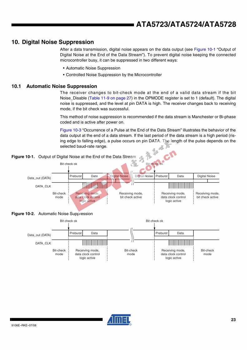
10. Digital Noise SuppressionAfter a data transmission, digital noise appears on the data output (see Figure 10-1 “Output ofDigital Noise at the End of the Data Stream”). To prevent digital noise keeping the connectedmicrocontroller busy, it can be suppressed in two different ways:
• Automatic Noise Suppression
• Controlled Noise Suppression by the Microcontroller
10.1 Automatic Noise SuppressionThe receiver changes to bit-check mode at the end of a valid data stream if the bitNoise_Disable (Table 11-9 on page 27) in the OPMODE register is set to 1 (default). The digitalnoise is suppressed, and the level at pin DATA is high. The receiver changes back to receivingmode, if the bit check was successful.
This method of noise suppression is recommended if the data stream is Manchester or Bi-phasecoded and is active after power on.
Figure 10-3 “Occurrence of a Pulse at the End of the Data Stream” illustrates the behavior of thedata output at the end of a data stream. If the last period of the data stream is a high period (ris-ing edge to falling edge), a pulse occurs on pin DATA. The length of the pulse depends on theselected baud-rate range.
Figure 10-1. Output of Digital Noise at the End of the Data Stream
Figure 10-2. Automatic Noise Suppression
DATA_CLK
Data_out (DATA)DataPreburst
Receiving mode,data clock control
logic active
Receiving mode,data clock control
logic active
Bit-checkmode
Bit check ok
Receiving mode,bit check active
Receiving mode,bit check active
Data Digital NoiseDigital NoiseDigital NoisePreburst
Bit check ok
DATA_CLK
Data_out (DATA)DataPreburst
Receiving mode,data clock control
logic active
Receiving mode,data clock control
logic active
Bit-checkmode
Bit-checkmode
Bit-checkmode
Bit check ok
DataPreburst
Bit check ok

249106E–RKE–07/08
ATA5723/ATA5724/ATA5728
Figure 10-3. Occurrence of a Pulse at the End of the Data Stream
10.2 Controlled Noise Suppression by the MicrocontrollerDigital noise appears at the end of a valid data stream if the bit Noise_Disable (see Table 11-9on page 27) in the OPMODE register is set to 0. To suppress the noise, the pin POLLING/_ONmust be set to low. The receiver remains in receiving mode. The OFF command then causes achange to start-up mode. The programmed sleep time (see Table 11-7 on page 27) is not exe-cuted because the level at pin POLLING/_ON is low; however, the bit check is active in thiscase. The OFF command also activates the bit check if the pin POLLING/_ON is held to low.The receiver changes back to receiving mode if the bit check was successful. To activate thepolling mode at the end of the data transmission, the pin POLLING/_ON must be set to high.This way of suppressing the noise is recommended if the data stream is not Manchester orBi-phase coded.
Figure 10-4. Controlled Noise Suppression
Data_out (DATA)
DATA_CLK
Dem_out
'1' '1'
Digital noiseData stream
Receiving mode,data clock control
logic active
Bit-check mode
'1'
tee < TLim_min or TLim_max < tee < tLim_min_2T or tee > TLim_max_2T Timing error
Tpulse
Tee
POLLING/_ON
(DATA_CLK)
Serial bi-directionaldata line DataPreburst
Receiving modeReceiving mode Start-upmode
Sleepmode
Bit-checkmode
Bit-checkmode
Bit check ok
Data Digital NoiseDigital NoisePreburst
OFF-command Bit check ok

259106E–RKE–07/08
ATA5723/ATA5724/ATA5728
11. Configuring the ReceiverThe ATA5723/ATA5724/ATA5728 receiver is configured using two 12-bit RAM registers calledOPMODE and LIMIT. The registers can be programmed by means of the bidirectional DATAport. If the register content has changed due to a voltage drop, this condition is indicated by athe output pattern called reset marker (RM). If this occurs, the receiver must be reprogrammed.After a Power-On Reset (POR), the registers are set to default mode. If the receiver is operatedin default mode, there is no need to program the registers. Table 11-3 on page 25 shows thestructure of the registers. According to Table 11-1, bit 1 defines whether the receiver is set backto polling mode using the OFF command (see “Receiving Mode” on page 15) or whether it isprogrammed. Bit 2 represents the register address. It selects the appropriate register to be pro-grammed. For high programming reliability, bit 15 (Stop bit), at the end of the programmingoperation, must be set to 0.
Table 11-1. Effect of Bit 1 and Bit 2 on Programming the Registers
Bit 1 Bit 2 Action
1 x The receiver is set back to polling mode (OFF command)
0 1 The OPMODE register is programmed
0 0 The LIMIT register is programmed
Table 11-2. Effect of Bit 15 on Programming the Register
Bit 15 Action
0 The values are written into the register (OPMODE or LIMIT)
1 The values are not written into the register
Table 11-3. Effect of the Configuration Words within the Registers
Bit 1 Bit 2 Bit 3 Bit 4 Bit 5 Bit 6 Bit 7 Bit 8 Bit 9 Bit 10 Bit 11 Bit 12 Bit 13 Bit 14 Bit 15
OFF command
1 – – – – – – – – – – – – – –
– OPMODE register –
0 1
BR_Range NBit-checkModu-lation
Sleep XSleepNoise
Suppression0
Baud1 Baud0 BitChk1 BitChk0ASK/ _FSK
Sleep4 Sleep3 Sleep2 Sleep1 Sleep0 XSleepStdNoise_Disable
Default values ofBit 3...14
0 0 0 1 0 0 0 1 1 0 0 1 –
– LIMIT register –
0 0
Lim_min Lim_max –
Lim_min5
Lim_min4
Lim_min3
Lim_min2
Lim_min1
Lim_min0
Lim_max5
Lim_max4
Lim_max3
Lim_max2
Lim_max1
Lim_max0
0
Defaultvalues ofBit 3...14
0 1 0 1 0 1 1 0 1 0 0 1 –
269106E–RKE–07/08
ATA5723/ATA5724/ATA5728
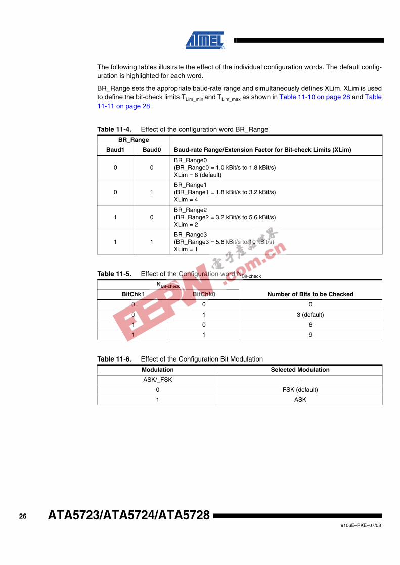
The following tables illustrate the effect of the individual configuration words. The default config-uration is highlighted for each word.
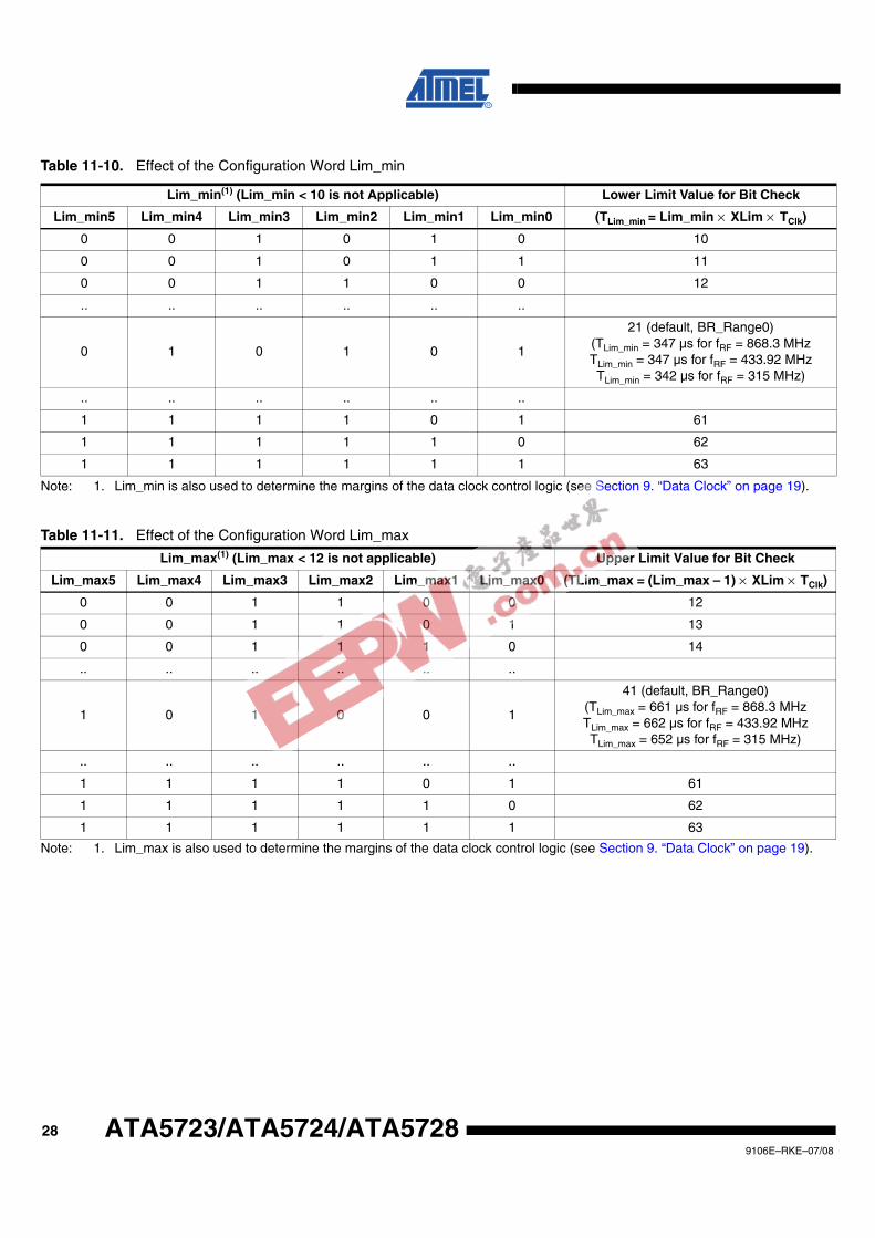
BR_Range sets the appropriate baud-rate range and simultaneously defines XLim. XLim is usedto define the bit-check limits TLim_min and TLim_max as shown in Table 11-10 on page 28 and Table11-11 on page 28.
Table 11-4. Effect of the configuration word BR_Range
BR_Range
Baud-rate Range/Extension Factor for Bit-check Limits (XLim)Baud1 Baud0
0 0BR_Range0 (BR_Range0 = 1.0 kBit/s to 1.8 kBit/s)XLim = 8 (default)
0 1BR_Range1 (BR_Range1 = 1.8 kBit/s to 3.2 kBit/s)XLim = 4
1 0BR_Range2 (BR_Range2 = 3.2 kBit/s to 5.6 kBit/s)XLim = 2
1 1BR_Range3 (BR_Range3 = 5.6 kBit/s to 10 kBit/s)XLim = 1
Table 11-5. Effect of the Configuration word NBit-check
NBit-check
Number of Bits to be CheckedBitChk1 BitChk0
0 0 0
0 1 3 (default)
1 0 6
1 1 9
Table 11-6. Effect of the Configuration Bit Modulation
Modulation Selected Modulation
ASK/_FSK –
0 FSK (default)
1 ASK
279106E–RKE–07/08
ATA5723/ATA5724/ATA5728
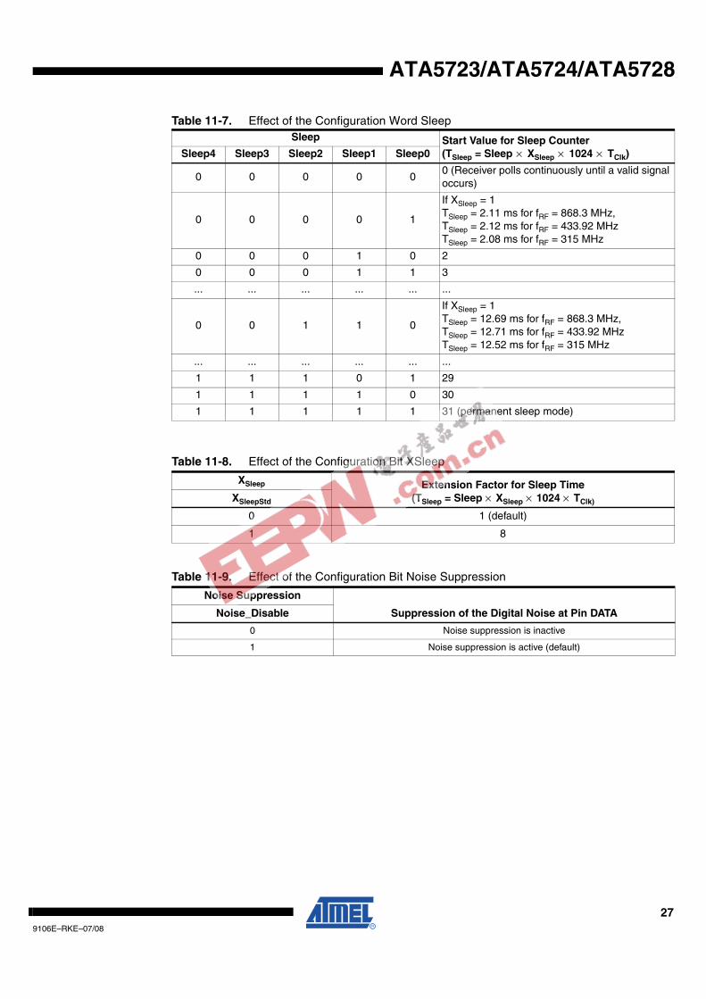
Table 11-7. Effect of the Configuration Word SleepSleep Start Value for Sleep Counter
(TSleep = Sleep × XSleep × 1024 × TClk)Sleep4 Sleep3 Sleep2 Sleep1 Sleep0
0 0 0 0 00 (Receiver polls continuously until a valid signal occurs)
0 0 0 0 1
If XSleep = 1TSleep = 2.11 ms for fRF = 868.3 MHz,TSleep = 2.12 ms for fRF = 433.92 MHzTSleep = 2.08 ms for fRF = 315 MHz
0 0 0 1 0 2
0 0 0 1 1 3
... ... ... ... ... ...
0 0 1 1 0
If XSleep = 1TSleep = 12.69 ms for fRF = 868.3 MHz,TSleep = 12.71 ms for fRF = 433.92 MHzTSleep = 12.52 ms for fRF = 315 MHz
... ... ... ... ... ...
1 1 1 0 1 29
1 1 1 1 0 30
1 1 1 1 1 31 (permanent sleep mode)
Table 11-8. Effect of the Configuration Bit XSleep
XSleep Extension Factor for Sleep Time (TSleep = Sleep × XSleep × 1024 × TClk)XSleepStd
0 1 (default)
1 8
Table 11-9. Effect of the Configuration Bit Noise Suppression
Noise Suppression
Suppression of the Digital Noise at Pin DATANoise_Disable
0 Noise suppression is inactive
1 Noise suppression is active (default)
289106E–RKE–07/08
ATA5723/ATA5724/ATA5728
Note: 1. Lim_min is also used to determine the margins of the data clock control logic (see Section 9. “Data Clock” on page 19).
Note: 1. Lim_max is also used to determine the margins of the data clock control logic (see Section 9. “Data Clock” on page 19).
Table 11-10. Effect of the Configuration Word Lim_min
Lim_min(1) (Lim_min < 10 is not Applicable) Lower Limit Value for Bit Check
Lim_min5 Lim_min4 Lim_min3 Lim_min2 Lim_min1 Lim_min0 (TLim_min = Lim_min × XLim × TClk)
0 0 1 0 1 0 10
0 0 1 0 1 1 11
0 0 1 1 0 0 12
.. .. .. .. .. ..
0 1 0 1 0 1
21 (default, BR_Range0)(TLim_min = 347 µs for fRF = 868.3 MHzTLim_min = 347 µs for fRF = 433.92 MHzTLim_min = 342 µs for fRF = 315 MHz)
.. .. .. .. .. ..
1 1 1 1 0 1 61
1 1 1 1 1 0 62
1 1 1 1 1 1 63
Table 11-11. Effect of the Configuration Word Lim_max
Lim_max(1) (Lim_max < 12 is not applicable) Upper Limit Value for Bit Check
Lim_max5 Lim_max4 Lim_max3 Lim_max2 Lim_max1 Lim_max0 (TLim_max = (Lim_max – 1) × XLim × TClk)
0 0 1 1 0 0 12
0 0 1 1 0 1 13
0 0 1 1 1 0 14
.. .. .. .. .. ..
1 0 1 0 0 1
41 (default, BR_Range0)(TLim_max = 661 µs for fRF = 868.3 MHzTLim_max = 662 µs for fRF = 433.92 MHzTLim_max = 652 µs for fRF = 315 MHz)
.. .. .. .. .. ..
1 1 1 1 0 1 61
1 1 1 1 1 0 62
1 1 1 1 1 1 63

299106E–RKE–07/08
ATA5723/ATA5724/ATA5728
12. Conservation of the Register InformationThe ATA5723/ATA5724 uses an integrated power-on reset and brown-out detection circuitry asa mechanism to preserve the RAM register information.
According to Figure 12-1, a power-on reset (POR) is generated if the supply voltage VS dropsbelow the threshold voltage VThReset. The default parameters are programmed into the configura-tion registers in that condition. The POR is cancelled after the minimum reset period tRst when VS
exceeds VThReset. A POR is also generated when the supply voltage of the receiver is turned on.
To indicate that condition, the receiver displays a reset marker (RM) at pin DATA after a reset.The RM is represented by the fixed frequency fRM at a 50% duty-cycle. RM can be cancelledusing a low pulse t1 at pin DATA. The RM has the following characteristics:
• fRM is lower than the lowest feasible frequency of a data signal. Due to this, RM cannot be misinterpreted by the connected microcontroller.
• If the receiver is set back to polling mode using pin DATA, RM cannot be cancelled accidentally if t1 is applied as described in the proposal in Section 13. “Programming the Configuration Register” on page 30.
Using this conservation mechanism, the receiver cannot lose its register information withoutcommunicating this condition using the reset marker RM.
Figure 12-1. Generation of the Power-on Reset
POR
Data_out (DATA) X
tRst
VThresetVS
1/fRM
309106E–RKE–07/08
ATA5723/ATA5724/ATA5728
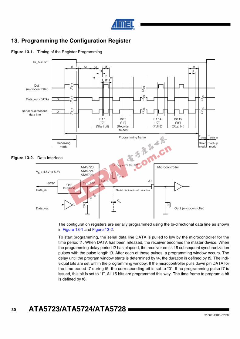
13. Programming the Configuration Register
Figure 13-1. Timing of the Register Programming
Figure 13-2. Data Interface
The configuration registers are serially programmed using the bi-directional data line as shownin Figure 13-1 and Figure 13-2.
To start programming, the serial data line DATA is pulled to low by the microcontroller for thetime period t1. When DATA has been released, the receiver becomes the master device. Whenthe programming delay period t2 has elapsed, the receiver emits 15 subsequent synchronizationpulses with the pulse length t3. After each of these pulses, a programming window occurs. Thedelay until the program window starts is determined by t4, the duration is defined by t5. The indi-vidual bits are set within the programming window. If the microcontroller pulls down pin DATA forthe time period t7 during t5, the corresponding bit is set to “0”. If no programming pulse t7 isissued, this bit is set to “1”. All 15 bits are programmed this way. The time frame to program a bitis defined by t6.
IC_ACTIVE
Serial bi-directionaldata line
Out1(microcontroller)
Data_out (DATA)
TSleep TStart-up
t7
Bit 2("1")
(Registerselect)
Bit 14("0")
(Poll 8)
Bit 15("0")
(Stop bit)
Bit 1("0")
(Start bit)
Programming frame
X
X
Receivingmode
Sleepmode
Start-upmode
t6
t8t4t1 t2 t3 t5 t9
InputInterface
Data_out Out1 (microcontroller)
Data_in
I/ODATA
VS = 4.5V to 5.5V
VX = 5V to 20V
Rpup
0V/5V 0V to 20V
MicrocontrollerATA5723ATA5724ATA5728
Serial bi-directional data line
ID
CL
319106E–RKE–07/08
ATA5723/ATA5724/ATA5728
Bit 15 is followed by the equivalent time window t9. During this window, the equivalenceacknowledge pulse t8 (E_Ack) occurs if the just programmed mode word is equivalent to themode word that was already stored in that register. E_Ack should be used to verify that themode word was correctly transferred to the register. The register must be programmed twice inthat case.
A register can be programmed when the receiver is in both sleep-mode and active mode. Duringprogramming, the LNA, LO, low-pass filter, IF-amplifier, and the FSK/MSK demodulator are dis-abled. The t1 pulse is used to start the programming or to switch the receiver back to pollingmode (OFF command). (The receiver is switched back to polling mode with the OFF command ifbit 1 is set to „1“.) The following convention should be considered for the length of the program-ming start pulse t1:
Using a t1 value of t1 (min) < t1 < 5632 TClk (where t1 (min) is the minimum specified value forthe relevant BR_Range) when the receiver is active i.e., not in reset mode initiates the program-ming or OFF command. However, if this t1 value is used when the receiver is in reset mode,programming or OFF command is NOT initiated and RM remains present at pin DATA. Note, theRM cannot be deleted when using this t1 value.
Using a t1 value of t1 > 7936 ´ TClk, programming or OFF command is initiated when thereceiver is in both reset mode and active mode. The registers PMODE and LIMIT are set to thedefault values and the RM is deleted, if present. This t1 values can be used if the connectedmicrocontroller detects an RM. Additionally, this t1 value can generally be used if the receiveroperates in default mode.
Note that the capacitive load at pin DATA is limited.

329106E–RKE–07/08
ATA5723/ATA5724/ATA5728
14. Data InterfaceThe data interface (see Figure 13-2 on page 30) is designed for automotive requirements. It canbe connected using the pull-up resistor Rpup up to 20V and is short-circuit-protected.
The applicable pull-up resistor Rpup depends on the load capacity CL at pin DATA and theselected BR_range (see Table 14-1).
Figure 14-1. Application Circuit: fRF = 315 MHz(1), 433.92 MHz or without SAW Filter
Note: For 315 MHz application pin MODE must be connected to GND.
Table 14-1. Applicable Rpup
- BR_range Applicable Rpup
CL ≤ 1nF
B0 1.6 kΩ to 47 kΩ
B1 1.6 kΩ to 22 kΩ
B2 1.6 kΩ to 12 kΩ
B3 1.6 kΩ to 5.6 kΩ
CL ≤ 100pF
B0 1.6 kΩ to 470 kΩ
B1 1.6 kΩ to 220 kΩ
B2 1.6 kΩ to 120 kΩ
B3 1.6 kΩ to 56 kΩ
11
12
13
14
15
16
17
18
19
20
3
10
9
8
7
6
5
4
2
1
LNAGND
LNA_IN
LNAREF
AGND
RSSI
TEST1
AVCC
CDEM
IC_ACTIVE
SENS
TEST2
TEST3
XTAL1
XTAL2
DVCC
MODE
DATA_CLK
DGND
POLLING/_ON
DATA
Fcrystal
CL2
R2
L1
GND
C16
C17RF_IN
VS
R31.6 kΩ
56 kΩ to 150 kΩ
CL1
DATA_CLK
Sensitivity reduction
POLLING/_ON
DATA
C1210 nF10%
C1310 nF10%
C1439 nF
5%
C74.7 µF10%
VX = 5V to 20V
IC_ACTIVE
RSSI
ATA5723ATA5724ATA5728
+
Table 14-2. Input Matching to 50Ω
RF Frequency (MHz)
LNA Matching Crystal Frequency fXTAL (MHz)C16 (pF) C17 (pF) L1 (nH)
315 Not connected 3 39 14.71875
433.92 Not connected 3 20 13.52875
868.3 1 3 6.8 13.55234

339106E–RKE–07/08
ATA5723/ATA5724/ATA5728
15. Absolute Maximum RatingsStresses beyond those listed under “Absolute Maximum Ratings” may cause permanent damage to the device. This is a stress rating only and functional operation of the device at these or any other conditions beyond those indicated in the operational sections of this specification is not implied. Exposure to absolute maximum rating conditions for extended periods may affect device reliability.
Parameters Symbol Min. Max. Unit
Supply voltage VS 6 V
Power dissipation Ptot 1000 mW
Junction temperature Tj 150 °C
Storage temperature Tstg –55 +125 °C
Ambient temperature Tamb –40 +105 °C
Maximum input level, input matched to 50Ω Pin_max 10 dBm
16. Thermal ResistanceParameters Symbol Value Unit
Junction ambient RthJA 100 K/W

349106E–RKE–07/08
ATA5723/ATA5724/ATA5728
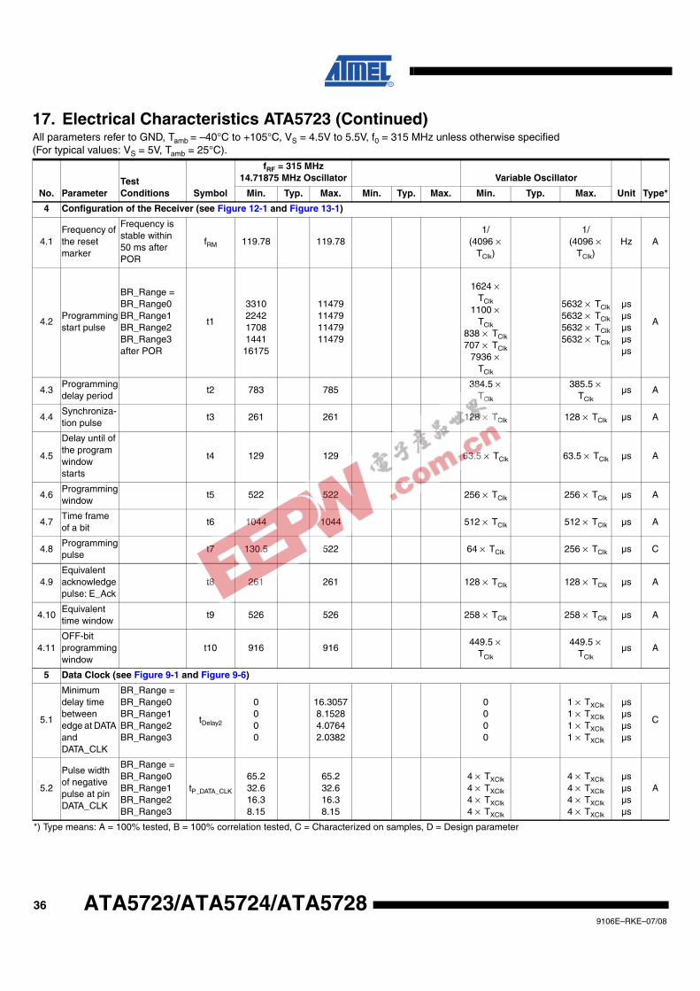
17. Electrical Characteristics ATA5723All parameters refer to GND, Tamb = –40°C to +105°C, VS = 4.5V to 5.5V, f0 = 315 MHz unless otherwise specified(For typical values: VS = 5V, Tamb = 25°C).
No. ParameterTest Conditions Symbol
fRF = 315 MHz14.71875 MHz Oscillator Variable Oscillator
Unit Type*Min. Typ. Max. Min. Typ. Max. Min. Typ. Max.
1 Basic Clock Cycle of the Digital Circuitry
1.1Basic clock cycle
TClk 2.0382 2.0382 30/fXTO 30/fXTO µs A
1.2Extended basic clock cycle
BR_Range0BR_Range1BR_Range2BR_Range3
TXClk
16.30578.15284.07642.0382
16.30578.15284.07642.0382
8 × TClk4 × TClk2 × TClk1 × TClk
8 × TClk4 × TClk2 × TClk1 × TClk
µsµsµsµs
A
2 Polling Mode
2.1
Sleep time (see Figure 8-1, Figure 8-10 and Figure 13-1)
Sleep and XSleep are defined in the OPMODE register
TSleep
Sleep × XSleep × 1024 × 2.0382
Sleep × XSleep × 1024 × 2.0382
Sleep × XSleep × 1024 ×
TClk
Sleep × XSleep ×
1024 × TClk
ms A
2.2
Start-up time (see Figure 8-1 and Figure 8-4)
BR_Range0BR_Range1BR_Range2BR_Range3
TStartup
182710441044653
182710441044653
896.5512.5512.5320.5× TClk
896.5512.5512.5320.5× TClk
µsµsµsµsµs
A
2.3Time for bit check (see Figure 8-1
Average bit-check time while polling,no RF applied (see Figure 8-5 and Figure 8-6)BR_Range0BR_Range1BR_Range2BR_Range3
TBit-check
0.450.240.140.08
0.450.240.140.08
msmsmsms
C
2.4Time for bit check (see Figure 8-1
Bit-check time for a valid input signal fSig (see Figure 8-5)NBit-check = 0NBit-check = 3NBit-check = 6NBit-check = 9
TBit-check1 × TXClk
3/fSig6/fSig9/fSig
1 × TXClk3.5/fSig6.5/fSig9.5/fSig
1 × TXClk3/fSig6/fSig9/fSig
1 × TClk3.5/fSig6.5/fSig9.5/fSig
msmsmsms
C
3 Receiving Mode
3.1Intermediate frequency
fIF 987 fIF = fLO/318 kHz A
3.2Baud-rate range
BR_Range0BR_Range1BR_Range2BR_Range3
BR_Range
1.01.83.25.6
1.83.25.6
10.0
BR_Range0 × 2 µs/TClk BR_Range1 × 2 µs/TClkBR_Range2 × 2 µs/TClkBR_Range3 × 2 µs/TClk
kBit/skBit/skBit/skBit/s
A
*) Type means: A = 100% tested, B = 100% correlation tested, C = Characterized on samples, D = Design parameter

359106E–RKE–07/08
ATA5723/ATA5724/ATA5728
3.3
Minimum time period between edges at pin DATA (see Figure 4-2 andFigure 8-8, Figure 8-9) (With the exception of parameter TPulse)
BR_Range =
BR_Range0BR_Range1BR_Range2BR_Range3
tDATA_min
163.0681.5340.7620.38
163.0681.5340.7620.38
10 × TXClk10 × TXClk10 × TXClk10 × TXClk
10 × TXClk10 × TXClk10 × TXClk10 × TXClk
µsµsµsµs
A
3.4
Maximum Low period at pin DATA(see Figure 4-2)
BR_Range =BR_Range0BR_Range1BR_Range2BR_Range3
tDATA_L_max
21201060530265
21201060530265
130 × TXClk130 × TXClk130 × TXClk130 × TXClk
130 × TXClk130 × TXClk130 × TXClk130 × TXClk
µsµsµsµs
A
3.5
Delay to activate the start-up mode (see Figure 8-12)
Ton1 19.36 21.4 9.5 × TClk 10.5 × TClk µs A
3.6
OFF command at pin POLLING/_ON (see Figure 8-11)
Ton2 16.3 8 × TClk µs A
3.7
Delay to activate the sleep mode(see Figure 8-11)
Ton3 17.32 19.36 8.5 × TClk 9.5 × TClk µs A
3.8
Pulse on pin DATA at the end of a data stream(see Figure 10-3)
BR_Range =BR_Range0BR_Range1BR_Range2BR_Range3
TPulse16.38.154.072.04
16.38.154.072.04
8 × TClk4 × TClk2 × TClk1 × TClk
8 × TClk4 × TClk2 × TClk1 × TClk
µsµsµsµs
C
17. Electrical Characteristics ATA5723 (Continued)All parameters refer to GND, Tamb = –40°C to +105°C, VS = 4.5V to 5.5V, f0 = 315 MHz unless otherwise specified(For typical values: VS = 5V, Tamb = 25°C).
No. ParameterTest Conditions Symbol
fRF = 315 MHz14.71875 MHz Oscillator Variable Oscillator
Unit Type*Min. Typ. Max. Min. Typ. Max. Min. Typ. Max.
*) Type means: A = 100% tested, B = 100% correlation tested, C = Characterized on samples, D = Design parameter
369106E–RKE–07/08
ATA5723/ATA5724/ATA5728
4 Configuration of the Receiver (see Figure 12-1 and Figure 13-1)
4.1Frequency of the reset marker
Frequency is stable within 50 ms after POR
fRM 119.78 119.781/
(4096 × TClk)
1/(4096 ×
TClk)Hz A
4.2Programming start pulse
BR_Range =BR_Range0BR_Range1BR_Range2BR_Range3after POR
t1
3310224217081441
16175
11479114791147911479
1624 × TClk
1100 × TClk
838 × TClk707 × TClk
7936 × TClk
5632 × TClk5632 × TClk5632 × TClk5632 × TClk
µsµsµsµsµs
A
4.3Programming delay period
t2 783 785384.5 ×
TClk
385.5 × TClk
µs A
4.4Synchroniza-tion pulse
t3 261 261 128 × TClk 128 × TClk µs A
4.5
Delay until of the program window starts
t4 129 129 63.5 × TClk 63.5 × TClk µs A
4.6Programming window
t5 522 522 256 × TClk 256 × TClk µs A
4.7Time frame of a bit
t6 1044 1044 512 × TClk 512 × TClk µs A
4.8Programming pulse
t7 130.5 522 64 × TClk 256 × TClk µs C
4.9Equivalent acknowledge pulse: E_Ack
t8 261 261 128 × TClk 128 × TClk µs A
4.10Equivalent time window
t9 526 526 258 × TClk 258 × TClk µs A
4.11OFF-bit programming window
t10 916 916449.5 ×
TClk
449.5 × TClk
µs A
5 Data Clock (see Figure 9-1 and Figure 9-6)
5.1
Minimum delay time between edge at DATA and DATA_CLK
BR_Range =BR_Range0BR_Range1BR_Range2BR_Range3
tDelay2
0000
16.30578.15284.07642.0382
0000
1 × TXClk1 × TXClk1 × TXClk1 × TXClk
µsµsµsµs
C
5.2
Pulse width of negative pulse at pin DATA_CLK
BR_Range =BR_Range0BR_Range1BR_Range2BR_Range3
tP_DATA_CLK
65.232.616.38.15
65.232.616.38.15
4 × TXClk4 × TXClk4 × TXClk4 × TXClk
4 × TXClk4 × TXClk4 × TXClk4 × TXClk
µsµsµsµs
A
17. Electrical Characteristics ATA5723 (Continued)All parameters refer to GND, Tamb = –40°C to +105°C, VS = 4.5V to 5.5V, f0 = 315 MHz unless otherwise specified(For typical values: VS = 5V, Tamb = 25°C).
No. ParameterTest Conditions Symbol
fRF = 315 MHz14.71875 MHz Oscillator Variable Oscillator
Unit Type*Min. Typ. Max. Min. Typ. Max. Min. Typ. Max.
*) Type means: A = 100% tested, B = 100% correlation tested, C = Characterized on samples, D = Design parameter

379106E–RKE–07/08
ATA5723/ATA5724/ATA5728
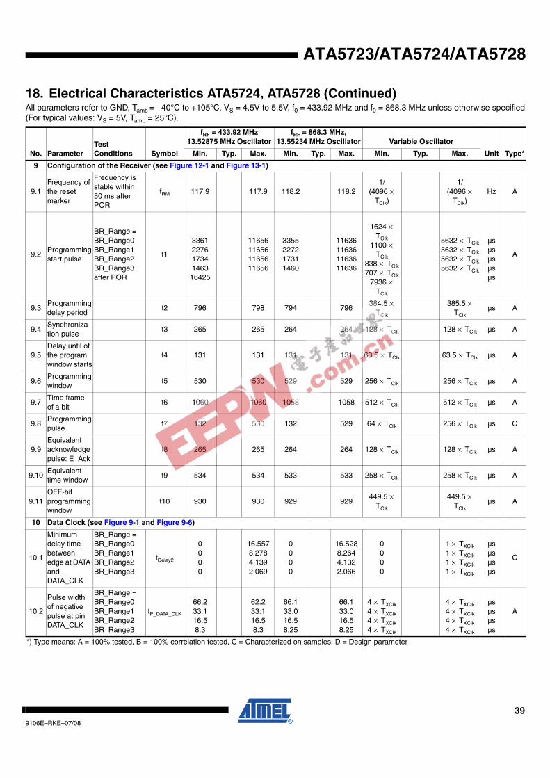
18. Electrical Characteristics ATA5724, ATA5728All parameters refer to GND, Tamb = –40°C to +105°C, VS = 4.5V to 5.5V, f0 = 433.92 MHz and f0 = 868.3 MHz unless otherwise specified(For typical values: VS = 5V, Tamb = 25°C).
No. ParameterTest Conditions Symbol
fRF = 433.92 MHz13.52875 MHz Oscillator
fRF = 868.3 MHz,13.55234 MHz Oscillator Variable Oscillator
Unit Type*Min. Typ. Max. Min. Typ. Max. Min. Typ. Max.
6 Basic Clock Cycle of the Digital Circuitry
6.1Basic clock cycle
TClk 2.0696 2.0696 2.066 2.066 28/fXTO 28/fXTO µs A
6.2Extended basic clock cycle
BR_Range0BR_Range1BR_Range2BR_Range3
TXClk
16.5578.2784.1392.069
16.5578.2784.1392.069
16.5288.2644.1322.066
16.5288.2644.1322.066
8 × TClk4 × TClk2 × TClk1 × TClk
8 × TClk4 × TClk2 × TClk1 × TClk
µsµsµsµs
A
7 Polling Mode
7.1
Sleep time (see Figure 8-1, Figure 8-10 and Figure 13-1)
Sleep and XSleep are defined in the OPMODE register
TSleep
Sleep × XSleep × 1024 × 2.0696
Sleep × XSleep × 1024 × 2.0696
Sleep × XSleep × 1024 × 2.066
Sleep × XSleep × 1024 × 2.066
Sleep × XSleep × 1024 ×
TClk
Sleep × XSleep ×
1024 × TClk
ms A
7.2
Start-up time (see Figure 8-1 and Figure 8-4)
BR_Range0BR_Range1BR_Range2BR_Range3
TStartup
185510601060663
185510601060663
185210581058662
185210581058662
896.5512.5512.5320.5× TClk
896.5512.5512.5320.5× TClk
µsµsµsµsµs
A
7.3Time for bit check (see Figure 8-1
Average bit-check time while polling,no RF applied (see Figure 8-8 on page 16 and Figure 8-9 on page 17)BR_Range0BR_Range1BR_Range2BR_Range3
TBit-check
0.450.240.140.08
0.450.240.140.08
0.450.240.140.08
msmsmsms
C
7.4Time for bit check (see Figure 8-1
Bit-check time for a valid input signal fSig (see Figure 8-5 on page 15)NBit-check = 0NBit-check = 3NBit-check = 6NBit-check = 9
TBit-check1 × TXClk
3/fSig6/fSig9/fSig
1 × TXClk3.5/fSig6.5/fSig9.5/fSig
1 × TXClk3/fSig6/fSig9/fSig
1 × TXClk3.5/fSig6.5/fSig9.5/fSig
1 × TXClk3/fSig6/fSig9/fSig
1 × TClk3.5/fSig6.5/fSig9.5/fSig
msmsmsms
C
8 Receiving Mode
8.1Intermediate frequency
fIF 987 947.9
fIF = fLO/438 for the 433.92 MHz band (ATA5724)
fIF = fLO/915 for the 868.3 MHz band (ATA5728)
kHz A
8.2Baud-rate range
BR_Range0BR_Range1BR_Range2BR_Range3
BR_Range
1.01.83.25.6
1.83.25.6
10.0
1.01.83.25.6
1.83.25.6
10.0
BR_Range0 × 2 µs/TClk BR_Range1 × 2 µs/TClkBR_Range2 × 2 µs/TClkBR_Range3 × 2 µs/TClk
kBit/skBit/skBit/skBit/s
A
*) Type means: A = 100% tested, B = 100% correlation tested, C = Characterized on samples, D = Design parameter

389106E–RKE–07/08
ATA5723/ATA5724/ATA5728
8.3
Minimum time period between edges at pin DATA (see Figure 4-2 andFigure 8-8, Figure 8-9) (With the exception of parameter TPulse)
BR_Range =
BR_Range0BR_Range1BR_Range2BR_Range3
tDATA_min
165.582.841.420.7
165.582.841.420.7
165.382.641.320.6
165.382.641.320.6
10 × TXClk10 × TXClk10 × TXClk10 × TXClk
10 × TXClk10 × TXClk10 × TXClk10 × TXClk
µsµsµsµs
A
8.4
Maximum Low period at pin DATA(see Figure 4-2)
BR_Range =BR_Range0BR_Range1BR_Range2BR_Range3
tDATA_L_max
21521076538269
21521076538269
21481074537
268.5
21481074537
268.5
130 × TXClk130 × TXClk130 × TXClk130 × TXClk
130 × TXClk130 × TXClk130 × TXClk130 × TXClk
µsµsµsµs
A
8.5
Delay to activate the start-up mode (see Figure 8-12)
Ton1 19.6 21.7 19.6 21.7 9.5 × TClk 10.5 × TClk µs A
8.6
OFF command at pin POLLING/_ON (see Figure 8-11)
Ton2 16.5 16.5 8 × TClk µs A
8.7
Delay to activate the sleep mode(see Figure 8-11)
Ton3 17.6 19.6 17.6 19.6 8.5 × TClk 9.5 × TClk µs A
8.8
Pulse on pin DATA at the end of a data stream(see Figure 10-3)
BR_Range =BR_Range0BR_Range1BR_Range2BR_Range3
TPulse16.5578.2784.1392.069
16.5578.2784.1392.069
16.5288.2644.1322.066
16.5288.2644.1322.066
8 × TClk4 × TClk2 × TClk1 × TClk
8 × TClk4 × TClk2 × TClk1 × TClk
µsµsµsµs
C
18. Electrical Characteristics ATA5724, ATA5728 (Continued)All parameters refer to GND, Tamb = –40°C to +105°C, VS = 4.5V to 5.5V, f0 = 433.92 MHz and f0 = 868.3 MHz unless otherwise specified(For typical values: VS = 5V, Tamb = 25°C).
No. ParameterTest Conditions Symbol
fRF = 433.92 MHz13.52875 MHz Oscillator
fRF = 868.3 MHz,13.55234 MHz Oscillator Variable Oscillator
Unit Type*Min. Typ. Max. Min. Typ. Max. Min. Typ. Max.
*) Type means: A = 100% tested, B = 100% correlation tested, C = Characterized on samples, D = Design parameter
399106E–RKE–07/08
ATA5723/ATA5724/ATA5728
9 Configuration of the Receiver (see Figure 12-1 and Figure 13-1)
9.1Frequency of the reset marker
Frequency is stable within 50 ms after POR
fRM 117.9 117.9 118.2 118.21/
(4096 × TClk)
1/(4096 ×
TClk)Hz A
9.2Programming start pulse
BR_Range =BR_Range0BR_Range1BR_Range2BR_Range3after POR
t1
3361227617341463
16425
11656116561165611656
3355227217311460
11636116361163611636
1624 × TClk
1100 × TClk
838 × TClk707 × TClk
7936 × TClk
5632 × TClk5632 × TClk5632 × TClk5632 × TClk
µsµsµsµsµs
A
9.3Programming delay period
t2 796 798 794 796384.5 ×
TClk
385.5 × TClk
µs A
9.4Synchroniza-tion pulse
t3 265 265 264 264 128 × TClk 128 × TClk µs A
9.5Delay until of the program window starts
t4 131 131 131 131 63.5 × TClk 63.5 × TClk µs A
9.6Programming window
t5 530 530 529 529 256 × TClk 256 × TClk µs A
9.7Time frame of a bit
t6 1060 1060 1058 1058 512 × TClk 512 × TClk µs A
9.8Programming pulse
t7 132 530 132 529 64 × TClk 256 × TClk µs C
9.9Equivalent acknowledge pulse: E_Ack
t8 265 265 264 264 128 × TClk 128 × TClk µs A
9.10Equivalent time window
t9 534 534 533 533 258 × TClk 258 × TClk µs A
9.11OFF-bit programming window
t10 930 930 929 929449.5 ×
TClk
449.5 × TClk
µs A
10 Data Clock (see Figure 9-1 and Figure 9-6)
10.1
Minimum delay time between edge at DATA and DATA_CLK
BR_Range =BR_Range0BR_Range1BR_Range2BR_Range3
tDelay2
0000
16.5578.2784.1392.069
0000
16.5288.2644.1322.066
0000
1 × TXClk1 × TXClk1 × TXClk1 × TXClk
µsµsµsµs
C
10.2
Pulse width of negative pulse at pin DATA_CLK
BR_Range =BR_Range0BR_Range1BR_Range2BR_Range3
tP_DATA_CLK
66.233.116.58.3
62.233.116.58.3
66.133.016.58.25
66.133.016.58.25
4 × TXClk4 × TXClk4 × TXClk4 × TXClk
4 × TXClk4 × TXClk4 × TXClk4 × TXClk
µsµsµsµs
A
18. Electrical Characteristics ATA5724, ATA5728 (Continued)All parameters refer to GND, Tamb = –40°C to +105°C, VS = 4.5V to 5.5V, f0 = 433.92 MHz and f0 = 868.3 MHz unless otherwise specified(For typical values: VS = 5V, Tamb = 25°C).
No. ParameterTest Conditions Symbol
fRF = 433.92 MHz13.52875 MHz Oscillator
fRF = 868.3 MHz,13.55234 MHz Oscillator Variable Oscillator
Unit Type*Min. Typ. Max. Min. Typ. Max. Min. Typ. Max.
*) Type means: A = 100% tested, B = 100% correlation tested, C = Characterized on samples, D = Design parameter

409106E–RKE–07/08
ATA5723/ATA5724/ATA5728
19. Electrical Characteristics ATA5723, ATA5724, ATA5728 All parameters refer to GND, Tamb = –40°C to +105°C, VS = 4.5V to 5.5V, f0 = 868.3 MHz, f0 = 433.92 MHz and f0 = 315 MHz, unless otherwise specified. (For typical values: VS = 5V, Tamb = 25°C)
No. Parameters Test Conditions Symbol Min. Typ. Max. Unit Type*
11 Current Consumption
11.1 Current consumption
Sleep mode(XTO and polling logic active)
ISoff 170 290 µA A
IC active (start-up-, bit-check-, receiving mode) Pin DATA = HFSKASK
ISon 8.58.0
11.010.4
mAmA
A
12 LNA, Mixer, Polyphase Low-pass and IF Amplifier (Input Matched According to Figure 14-1 on page 32 Referred to RFIN)
12.1 Third-order intercept point
LNA/mixer/IF amplifier868 MHz433 MHz315 MHz
IIP3–18–23–24
dBm C
12.2 LO spurious emission Required according to I-ETS 300220 ISLORF –70 –57 dBm A
12.3 System noise figure With power matching |S11| < –10 dB NF 5 dB B
12.4 LNA_IN input impedance
At 868.3 MHz
AT 433.92 MHz
At 315 MHz
ZiLNA_IN
(14.15 – j73.53)
(19.3 – j113.3)
(26.97 – j158.7)
Ω
Ω
Ω
C
12.5 1 dB compression point At 868.3 MHz AT 433.92 MHzAt 315 MHz
IP1db
–27.7–32.7–33.7
dBm C
12.6 Image rejection Within the complete image band 20 30 dB A
12.7 Maximum input levelBER ≤ 10-3,FSK modeASK mode
Pin_max –10–10
dBmdBm
C
13 Local Oscillator
13.1Operating frequency range VCO
ATA5728ATA5724ATA5723
fVCO
868431.5312.5
870436.5317.5
MHzMHzMHz
A
13.2 Phase noise local oscillatorfosc = 868.3 MHz at 10 MHzfosc = 433.92 MHz at 10 MHzfosc = 315 MHz at 10 MHz
L (fm)–140–143–143
–130–133–133
dBC/Hz B
13.3 Spurious of the VCO At ±fXTO –55 –45 dBC B
13.4 XTO pulling
XTO pulling,appropriate load capacitance must be connected to XTAL, crystal CL1 and CL2fXTAL = 14.71875 MHz (315 MHz band)fXTAL = 13.52875 MHz (433 MHz band)fXTAL = 13.55234 MHz (868 MHz band)
fXTO –10ppm fXTAL +10ppm MHz
B
13.5Series resonance resistor of the crystal
Parameter of the supplied crystal RS 120 Ω B
*) Type means: A = 100% tested, B = 100% correlation tested, C = Characterized on samples, D = Design parameter

419106E–RKE–07/08
ATA5723/ATA5724/ATA5728
13.6Static capacitance at pin XTAL1 to GND
Parameter of the supplied crystal and board parasitics
CL1 –5% 18 +5% pF B
13.7Static capacitance at pin XTAL2 to GND
Parameter of the supplied crystal and board parasitics
CL2 –5% 18 +5% pF B
13.8Crystal series resistor Rm at start-up
C0 < 1.8 pF, CL = 9 pF fXTAL = 14.71875 MHz
1.5 kΩ B
C0 < 2.0 pF, CL = 9 pF fXTAL = 13.52875 MHzfXTAL = 13.55234 MHz
1.5 kΩ B
14 Analog Signal Processing (Input Matched According to Figure 14-1 on page 32 Referred to RFIN)
14.1Input sensitivity ASK300 kHz IF Filter(ATA5723/ATA5724)
ASK (level of carrier) BER ≤ 10-3, 100% Modfin = 315 MHz/433.92 MHzVS = 5V, Tamb = 25°CfIF = 987 kHz
PRef_ASKBR_Range0 –111 –113 –115 dBm B
BR_Range1 –109.5 –111.5 –113.5 dBm B
BR_Range2 –109 –111 –113 dBm B
BR_Range3 –107 –109 –111 dBm B
14.2Input sensitivity ASK600 kHz IF Filter(ATA5728)
ASK (level of carrier) BER ≤ 10-3, 100% Modfin = 868.3 MHz VS = 5V, Tamb = 25°CfIF = 948 kHz
PRef_ASKBR_Range0 –109 –111 –113 dBm B
BR_Range1 –107.5 –109.5 –111.5 dBm B
BR_Range2 –107 –109 –111 dBm B
BR_Range3 –105 –107 –109 dBm B
14.3
Sensitivity variation ASK for the full operating range compared to Tamb = 25°C, VS = 5V(ATA5723/ATA5724/ATA5728)
300 kHz and 600 kHzfin = 315 MHz/433.92 MHz/868.3 MHzPASK = PRef_ASK + ΔPRef
ΔPRef +2.5 –1.5 dB B
14.4
Sensitivity variation ASK for full operating range including IF filter compared to Tamb = 25°C, VS = 5V
300 kHz version (ATA5723/ATA5724)fin = 315 MHz/433.92 MHzfIF = 987 kHzfIF = –110 kHz to +110 kHzfIF = –140 kHz to +140 kHzPASK = PRef_ASK + ΔPRef
ΔPRef +5.5+7.5
–1.5–1.5
dBdB
B
600 kHz version (ATA5728)fin = 868.3 MHzfIF = 948 kHzfIF = –210 kHz to +210 kHzfIF = –270 kHz to +270 kHzPASK = PRef_ASK + ΔPRef
ΔPRef +5.5+7.5
–1.5–1.5
dBdB
B
19. Electrical Characteristics ATA5723, ATA5724, ATA5728 (Continued)All parameters refer to GND, Tamb = –40°C to +105°C, VS = 4.5V to 5.5V, f0 = 868.3 MHz, f0 = 433.92 MHz and f0 = 315 MHz, unless otherwise specified. (For typical values: VS = 5V, Tamb = 25°C)
No. Parameters Test Conditions Symbol Min. Typ. Max. Unit Type*
*) Type means: A = 100% tested, B = 100% correlation tested, C = Characterized on samples, D = Design parameter

429106E–RKE–07/08
ATA5723/ATA5724/ATA5728
14.5Input sensitivity FSK 300 kHz IF filter(ATA5723/ATA5724)
BER ≤ 10-3
fin = 315 MHz/433.92 MHzVS = 5V, Tamb = 25°CfIF = 987 kHz
BR_Range0df = ±16 kHzdf = ±10 kHz to ±30 kHz
PRef_FSK –104–102
–107 –108.5–108.5
dBmdBm
B
BR_Range1df = ±16 kHzdf = ±10 kHz to ±30 kHz
PRef_FSK –102–100
–105 –106.5–106.5
dBmdBm
B
BR_Range2df = ±16 kHzdf = ±10 kHz to ±30 kHz
PRef_FSK –100.5–98.5
–103.5 –105–105
dBmdBm
B
BR_Range3df = ±16 kHzdf = ±10 kHz to ±30 kHz
PRef_FSK –98.5–96.5
–101.5 –103–103
dBmdBm
B
14.6Input sensitivity FSK 600 kHz IF filter(ATA5728)
BER ≤ 10-3
fin = 868.3 MHzVS = 5V, Tamb = 25°CfIF = 948 kHz
BR_Range0df = ±16 kHz to ±28 kHzdf = ±10 kHz to ±100 kHz
PRef_FSK –102–100
–105 –106.5–106.5
dBmdBm
B
BR_Range1df = ±16 kHz ±28 kHzdf = ±10 kHz to ±100 kHz
PRef_FSK –100–98
–103 –104.5–104.5
dBmdBm
B
BR_Range2df = ±18 kHz ±31 kHzdf = ±13 kHz to ±100 kHz
PRef_FSK –98.5–96.5
–101.5 –103–103
dBmdBm
B
BR_Range3df = ±25 kHz ±44 kHzdf = ±20 kHz to ±100 kHz
PRef_FSK –96.5–94.5
–99.5 –101–101
dBmdBm
B
14.7
Sensitivity variation FSK for the full operating range compared to Tamb = 25°C, VS = 5V(ATA5723/ATA5724/ATA5728)
300 kHz and 600 kHz versionsfin = 315 MHz/433.92 MHz/868.3 MHzPFSK = PRef_FSK + ΔPRef
ΔPRef +3 –1.5 dB B
19. Electrical Characteristics ATA5723, ATA5724, ATA5728 (Continued)All parameters refer to GND, Tamb = –40°C to +105°C, VS = 4.5V to 5.5V, f0 = 868.3 MHz, f0 = 433.92 MHz and f0 = 315 MHz, unless otherwise specified. (For typical values: VS = 5V, Tamb = 25°C)
No. Parameters Test Conditions Symbol Min. Typ. Max. Unit Type*
*) Type means: A = 100% tested, B = 100% correlation tested, C = Characterized on samples, D = Design parameter

439106E–RKE–07/08
ATA5723/ATA5724/ATA5728
14.8
Sensitivity variation FSK for the full operating range including IF filter compared to Tamb = 25°C, VS = 5V
300 kHz version (ATA5723/ATA5724)fin = 315 MHz/433.92 MHzfIF = 987 kHzfIF = –110 kHz to +110 kHzfIF = –140 kHz to +140 kHzfIF = –180 kHz to +180 kHzPFSK = PRef_FSK + ΔPRef
ΔPRef+6+8
+11
–2–2–2
dBdBdB
B
600 kHz version (ATA5728)fin = 868.3 MHzfIF = 948 kHzfIF = –150 kHz to +150 kHzfIF = –200 kHz to +200 kHzfIF = –260 kHz to +150 kHzPFSK = PRef_FSK + ΔPRef
ΔPRef+6+8
+11
–2–2–2
dBdBdB
B
14.9
S/N ratio to suppress in-band noise signals. Noise signals may have any modulation scheme
ASK modeFSK mode
SNRASKSNRFSK
102
123
dBdB
C
14.10 Dynamic range RSSI amplifier ΔRRSSI 60 dB A
14.11 RSSI output voltage range VRSSI 1 3.5 V A
14.12 RSSI gain GRSSI 20 mV/dB A
14.13Lower cut-off frequency of the data filter
CDEM = 33 nF
fcu_DF 0.11 0.16 0.20 kHz B
14.14Recommended CDEM for best performance
BR_Range0 (default)BR_Range1BR_Range2BR_Range3
CDEM
3922128.2
nFnFnFnF
C
14.15Edge-to-edge time period of the input data signal for full sensitivity
BR_Range0 (default)BR_Range1BR_Range2BR_Range3
tee_sig
2701568950
1000560320180
msmsmsms
C
14.16Upper cut-off frequency data filter
Upper cut-off frequency programmable in 4 ranges using a serial mode wordBR_Range0 (default)BR_Range1BR_Range2BR_Range3
fu2.84.88.0
15.0
3.46.0
10.019.0
4.07.2
12.023.0
kHzkHzkHzkHz
B
14.17 Reduced sensitivity
300 kHz version (ATA5723/ATA5724)RSense connected from pin SENSto VS, input matched according to Figure 14-1 “Application Circuit, fin = 315 MHz/433.92 MHz, VS = 5V, Tamb = +25°C
dBm (peak level)
RSense = 56 kΩ PRef_Red –74 –79 –83 dBm B
RSense = 100 kΩ PRef_Red –83 –88 –93 dBm B
19. Electrical Characteristics ATA5723, ATA5724, ATA5728 (Continued)All parameters refer to GND, Tamb = –40°C to +105°C, VS = 4.5V to 5.5V, f0 = 868.3 MHz, f0 = 433.92 MHz and f0 = 315 MHz, unless otherwise specified. (For typical values: VS = 5V, Tamb = 25°C)
No. Parameters Test Conditions Symbol Min. Typ. Max. Unit Type*
*) Type means: A = 100% tested, B = 100% correlation tested, C = Characterized on samples, D = Design parameter
fcu_DF1
2 π× 30 kΩ× CDEM×-------------------------------------------------------------=

449106E–RKE–07/08
ATA5723/ATA5724/ATA5728
14.18 Reduced sensitivity
600 kHz version (ATA5728)RSense connected from pin SENSto VS, input matched according to Figure 14-1 “Application Circuit, fin = 868.3 MHz, VS = 5V, Tamb = +25°C
dBm (peak level)
RSense = 56 kΩ PRef_Red –63 –68 –73 dBm B
RSense = 100 kΩ PRef_Red –72 –77 –82 dBm B
14.19Reduced sensitivity variation over full operating range
RSense = 56 kΩRSense = 100 kΩPRed = PRef_Red + ΔPRed
ΔPRed
55
00
00
dBdB C
14.20Reduced sensitivity variation for different values of RSense
Values relative to RSense = 56 kΩRSense = 56 kΩRSense = 68 kΩRSense = 82 kΩRSense = 100 kΩ
ΔPRed
0–3.5–6.0–9.0
dBdBdBdB
C
14.21 Threshold voltage for reset VThRESET 1.95 2.8 3.75 V A
15 Digital Ports
15.1
Data output- Saturation voltage Low
- max voltage at pin DATA- quiescent current - short-circuit current- ambient temp. in case of
permanent short-circuit Data input- Input voltage Low- Input voltage High
Iol ≤ 12 mAIol = 2 mA
Voh = 20VVol = 0.8V to 20VVoh = 0V to 20V
VolVolVohIqu
Iol_limtamb_sc
VIlVich
13
0.65 × VS
0.350.08
30
0.80.320204585
0.35 × VS
VVV
µAmA°C
VV
A
15.2DATA_CLK output- Saturation voltage Low- Saturation voltage High
IDATA_CLK = 1mAIDATA_CLK = –1mA
VolVoh VS – 0.4V
0.1VS –
0.15V
0.4 VV
A
15.3IC_ACTIVE output- Saturation voltage Low- Saturation voltage High
IIC_ACTIVE = 1 mAIIC_ACTIVE = –1 mA
VolVoh
VS – 0.4 V
0.1VS –
0.15V
0.4 VV
A
15.4POLLING/_ON input- Low level input voltage- High level input voltage
Receiving modePolling mode
VIlVIh 0.8 × VS
0.2 × VS VV
A
15.5MODE pin- High level input voltage
Test input must always be set to HighVIh 0.8 × VS V
A
15.6TEST 1 pin- Low level input voltage
Test input must always be set to LowVIl 0.2 × VS V
A
19. Electrical Characteristics ATA5723, ATA5724, ATA5728 (Continued)All parameters refer to GND, Tamb = –40°C to +105°C, VS = 4.5V to 5.5V, f0 = 868.3 MHz, f0 = 433.92 MHz and f0 = 315 MHz, unless otherwise specified. (For typical values: VS = 5V, Tamb = 25°C)
No. Parameters Test Conditions Symbol Min. Typ. Max. Unit Type*
*) Type means: A = 100% tested, B = 100% correlation tested, C = Characterized on samples, D = Design parameter

459106E–RKE–07/08
ATA5723/ATA5724/ATA5728
21. Package Information
20. Ordering InformationExtended Type Number Package Remarks
ATA5723P3-TKQY SSO20 315 MHz version
ATA5724P3-TKQY SSO20 433 MHz version
ATA5728P6-TKQY SSO20 868 MHz version
Package: SSO20Dimensions in mm
specificationsaccording to DINtechnical drawings
6.75-0.25
1120
101
Issue: 1; 10.03.04
Drawing-No.: 6.543-5056.01-4
5.85±0.05
1.3±
0.05
0.15
±0.
05
0.65±0.05
5.4±0.2
4.4±0.1
6.45±0.150.25±0.05
0.05
+0.
1

9106E–RKE–07/08
Headquarters International
Atmel Corporation2325 Orchard ParkwaySan Jose, CA 95131USATel: 1(408) 441-0311Fax: 1(408) 487-2600
Atmel AsiaRoom 1219Chinachem Golden Plaza77 Mody Road TsimshatsuiEast KowloonHong KongTel: (852) 2721-9778Fax: (852) 2722-1369
Atmel EuropeLe Krebs8, Rue Jean-Pierre TimbaudBP 30978054 Saint-Quentin-en-Yvelines CedexFranceTel: (33) 1-30-60-70-00 Fax: (33) 1-30-60-71-11
Atmel Japan9F, Tonetsu Shinkawa Bldg.1-24-8 ShinkawaChuo-ku, Tokyo 104-0033JapanTel: (81) 3-3523-3551Fax: (81) 3-3523-7581
Product Contact
Web Sitewww.atmel.com
Technical [email protected]
Sales Contactwww.atmel.com/contacts
Literature Requestswww.atmel.com/literature
Disclaimer: The information in this document is provided in connection with Atmel products. No license, express or implied, by estoppel or otherwise, to anyintellectual property right is granted by this document or in connection with the sale of Atmel products. EXCEPT AS SET FORTH IN ATMEL’S TERMS AND CONDI-TIONS OF SALE LOCATED ON ATMEL’S WEB SITE, ATMEL ASSUMES NO LIABILITY WHATSOEVER AND DISCLAIMS ANY EXPRESS, IMPLIED OR STATUTORYWARRANTY RELATING TO ITS PRODUCTS INCLUDING, BUT NOT LIMITED TO, THE IMPLIED WARRANTY OF MERCHANTABILITY, FITNESS FOR A PARTICULARPURPOSE, OR NON-INFRINGEMENT. IN NO EVENT SHALL ATMEL BE LIABLE FOR ANY DIRECT, INDIRECT, CONSEQUENTIAL, PUNITIVE, SPECIAL OR INCIDEN-TAL DAMAGES (INCLUDING, WITHOUT LIMITATION, DAMAGES FOR LOSS OF PROFITS, BUSINESS INTERRUPTION, OR LOSS OF INFORMATION) ARISING OUT OFTHE USE OR INABILITY TO USE THIS DOCUMENT, EVEN IF ATMEL HAS BEEN ADVISED OF THE POSSIBILITY OF SUCH DAMAGES. Atmel makes norepresentations or warranties with respect to the accuracy or completeness of the contents of this document and reserves the right to make changes to specificationsand product descriptions at any time without notice. Atmel does not make any commitment to update the information contained herein. Unless specifically providedotherwise, Atmel products are not suitable for, and shall not be used in, automotive applications. Atmel’s products are not intended, authorized, or warranted for useas components in applications intended to support or sustain life.
© 2008 Atmel Corporation. All rights reserved. Atmel®, logo and combinations thereof, and others are registered trademarks or trademarks ofAtmel Corporation or its subsidiaries. Other terms and product names may be trademarks of others.


