This is information on a product in full production.
March 2018 DS11840 Rev 6 1/91
ST25RU3993
UHF RFID single chip reader EPC Class1 Gen2 compatible
Datasheet - production data
Features
• Supply voltage range 3.0 to 3.6 V
– Limited operation possible down to 2.7 V
– Maximum PA supply voltage 4.3 V
– Peripheral I/O supply range 1.65 to 5.5 V
• Protocol support for:
– ISO 18000-6C (EPC Class1 Gen2)
– ISO 29143 (Air interface for mobile RFID)
– ISO 18000-6A/B through direct mode
• DRM: 250 kHz and 320 kHz filters for M4 and M8
• Integrated supply regulators
• Frequency hopping support
• ASK or PR-ASK modulation
• Automatic I/Q selection
• Phase bit for tag tracking with 8-bit linear RSSI
• Temperature range: -40 °C to 85 °C
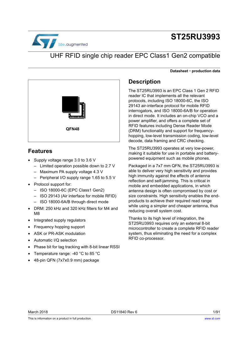
• 48-pin QFN (7x7x0.9 mm) package
Description
The ST25RU3993 is an EPC Class 1 Gen 2 RFID reader IC that implements all the relevant protocols, including ISO 18000-6C, the ISO 29143 air-interface protocol for mobile RFID interrogators, and ISO 18000-6A/B for operation in direct mode. It includes an on-chip VCO and a power amplifier, and offers a complete set of RFID features including Dense Reader Mode (DRM) functionality and support for frequency-hopping, low-level transmission coding, low-level decode, data framing and CRC checking.
The ST25RU3993 operates at very low-power, making it suitable for use in portable and battery-powered equipment such as mobile phones.
Packaged in a 7x7 mm QFN, the ST25RU3993 is able to deliver very high sensitivity and provides high immunity against the effects of antenna reflection and self-jamming. This is critical in mobile and embedded applications, in which antenna design is often compromised by cost or size constraints. High sensitivity enables the end-products to achieve their required read range while using a simpler and cheaper antenna, thus reducing overall system cost.
Thanks to its high level of integration, the ST25RU3993 requires only an external 8-bit microcontroller to create a complete RFID reader system, thus eliminating the need for a complex RFID co-processor.
QFN48
www.st.com
Contents ST25RU3993
2/91 DS11840 Rev 6
Contents
1 Description . . . . . . . . . . . . . . . . . . . . . . . . . . . . . . . . . . . . . . . . . . . . . . . . . 9
1.1 Block diagram . . . . . . . . . . . . . . . . . . . . . . . . . . . . . . . . . . . . . . . . . . . . . . . 9
2 Functional overview . . . . . . . . . . . . . . . . . . . . . . . . . . . . . . . . . . . . . . . . 10
2.1 Power supply . . . . . . . . . . . . . . . . . . . . . . . . . . . . . . . . . . . . . . . . . . . . . . 12
2.1.1 Main regulators . . . . . . . . . . . . . . . . . . . . . . . . . . . . . . . . . . . . . . . . . . . 12
2.1.2 Internal PA supply regulator . . . . . . . . . . . . . . . . . . . . . . . . . . . . . . . . . . 12
2.1.3 Periphery communication supply . . . . . . . . . . . . . . . . . . . . . . . . . . . . . . 12
2.1.4 Automatic power supply level setting . . . . . . . . . . . . . . . . . . . . . . . . . . . 12
2.1.5 Power modes . . . . . . . . . . . . . . . . . . . . . . . . . . . . . . . . . . . . . . . . . . . . . 13
2.2 Host communication . . . . . . . . . . . . . . . . . . . . . . . . . . . . . . . . . . . . . . . . . 14
2.2.1 Writing to registers . . . . . . . . . . . . . . . . . . . . . . . . . . . . . . . . . . . . . . . . . 16
2.2.2 Reading from registers . . . . . . . . . . . . . . . . . . . . . . . . . . . . . . . . . . . . . 17
2.2.3 Direct commands . . . . . . . . . . . . . . . . . . . . . . . . . . . . . . . . . . . . . . . . . . 18
2.2.4 SPI interface timing . . . . . . . . . . . . . . . . . . . . . . . . . . . . . . . . . . . . . . . . 22
2.2.5 CLSYS output . . . . . . . . . . . . . . . . . . . . . . . . . . . . . . . . . . . . . . . . . . . . 24
2.2.6 IO signal level and output characteristics . . . . . . . . . . . . . . . . . . . . . . . 25
2.2.7 OAD, OAD2 outputs . . . . . . . . . . . . . . . . . . . . . . . . . . . . . . . . . . . . . . . 25
2.3 PLL and VCO section . . . . . . . . . . . . . . . . . . . . . . . . . . . . . . . . . . . . . . . . 25
2.3.1 Voltage controlled oscillator . . . . . . . . . . . . . . . . . . . . . . . . . . . . . . . . . . 26
2.3.2 PLL prescaler and main divider . . . . . . . . . . . . . . . . . . . . . . . . . . . . . . . 27
2.3.3 PLL reference frequency . . . . . . . . . . . . . . . . . . . . . . . . . . . . . . . . . . . . 27
2.3.4 Reference frequency source . . . . . . . . . . . . . . . . . . . . . . . . . . . . . . . . . 27
2.3.5 Phase-frequency detector and charge pump . . . . . . . . . . . . . . . . . . . . . 28
2.3.6 Loop filter . . . . . . . . . . . . . . . . . . . . . . . . . . . . . . . . . . . . . . . . . . . . . . . . 28
2.3.7 Frequency hopping commands . . . . . . . . . . . . . . . . . . . . . . . . . . . . . . . 28
2.3.8 PLL start-up and frequency hopping . . . . . . . . . . . . . . . . . . . . . . . . . . . 28
2.4 Device status control . . . . . . . . . . . . . . . . . . . . . . . . . . . . . . . . . . . . . . . . 28
2.5 Protocol control . . . . . . . . . . . . . . . . . . . . . . . . . . . . . . . . . . . . . . . . . . . . 29
2.6 Transmission section . . . . . . . . . . . . . . . . . . . . . . . . . . . . . . . . . . . . . . . . 29
2.6.1 Tx data handling and coding . . . . . . . . . . . . . . . . . . . . . . . . . . . . . . . . . 30
2.6.2 Tx shape circuitry . . . . . . . . . . . . . . . . . . . . . . . . . . . . . . . . . . . . . . . . . . 30
2.6.3 Local oscillator (LO) path . . . . . . . . . . . . . . . . . . . . . . . . . . . . . . . . . . . . 30
2.6.4 Modulator . . . . . . . . . . . . . . . . . . . . . . . . . . . . . . . . . . . . . . . . . . . . . . . . 31
DS11840 Rev 6 3/91
ST25RU3993 Contents
5
2.7 Tx outputs . . . . . . . . . . . . . . . . . . . . . . . . . . . . . . . . . . . . . . . . . . . . . . . . . 31
2.8 Tx operation modes . . . . . . . . . . . . . . . . . . . . . . . . . . . . . . . . . . . . . . . . . 32
2.8.1 TX normal mode . . . . . . . . . . . . . . . . . . . . . . . . . . . . . . . . . . . . . . . . . . 32
2.8.2 TX direct mode . . . . . . . . . . . . . . . . . . . . . . . . . . . . . . . . . . . . . . . . . . . 33
2.9 Receiver . . . . . . . . . . . . . . . . . . . . . . . . . . . . . . . . . . . . . . . . . . . . . . . . . . 34
2.9.1 Input mixers . . . . . . . . . . . . . . . . . . . . . . . . . . . . . . . . . . . . . . . . . . . . . . 35
2.9.2 Local oscillator path . . . . . . . . . . . . . . . . . . . . . . . . . . . . . . . . . . . . . . . . 36
2.9.3 Fast AC coupling . . . . . . . . . . . . . . . . . . . . . . . . . . . . . . . . . . . . . . . . . . 36
2.9.4 Rx filter . . . . . . . . . . . . . . . . . . . . . . . . . . . . . . . . . . . . . . . . . . . . . . . . . . 36
2.9.5 IQ selection . . . . . . . . . . . . . . . . . . . . . . . . . . . . . . . . . . . . . . . . . . . . . . 39
2.9.6 Bit decoder . . . . . . . . . . . . . . . . . . . . . . . . . . . . . . . . . . . . . . . . . . . . . . . 40
2.9.7 Data framer . . . . . . . . . . . . . . . . . . . . . . . . . . . . . . . . . . . . . . . . . . . . . . 40
2.10 Data reception modes . . . . . . . . . . . . . . . . . . . . . . . . . . . . . . . . . . . . . . . 40
2.10.1 Rx normal mode . . . . . . . . . . . . . . . . . . . . . . . . . . . . . . . . . . . . . . . . . . 40
2.10.2 Rx direct mode . . . . . . . . . . . . . . . . . . . . . . . . . . . . . . . . . . . . . . . . . . . . 43
2.10.3 Modes supporting tuning of antenna or directivity device . . . . . . . . . . . 44
2.10.4 Logarithmic RSSI . . . . . . . . . . . . . . . . . . . . . . . . . . . . . . . . . . . . . . . . . . 44
2.11 A/D converter . . . . . . . . . . . . . . . . . . . . . . . . . . . . . . . . . . . . . . . . . . . . . . 44
2.11.1 External RF power detector . . . . . . . . . . . . . . . . . . . . . . . . . . . . . . . . . . 44
2.11.2 Reflected RF power indicator . . . . . . . . . . . . . . . . . . . . . . . . . . . . . . . . 45
2.11.3 Supply voltage measurement . . . . . . . . . . . . . . . . . . . . . . . . . . . . . . . . 45
2.11.4 Linear RSSI with sub-carrier phase bit . . . . . . . . . . . . . . . . . . . . . . . . . 45
2.11.5 Internal signal level detectors . . . . . . . . . . . . . . . . . . . . . . . . . . . . . . . . 46
2.12 Interrogator anti-collision support . . . . . . . . . . . . . . . . . . . . . . . . . . . . . . . 46
3 Register description . . . . . . . . . . . . . . . . . . . . . . . . . . . . . . . . . . . . . . . . 47
3.1 Main control registers . . . . . . . . . . . . . . . . . . . . . . . . . . . . . . . . . . . . . . . . 48
3.1.1 Device status control register . . . . . . . . . . . . . . . . . . . . . . . . . . . . . . . . 49
3.1.2 Protocol selection register . . . . . . . . . . . . . . . . . . . . . . . . . . . . . . . . . . . 49
3.2 Configuration registers . . . . . . . . . . . . . . . . . . . . . . . . . . . . . . . . . . . . . . . 50
3.2.1 Tx options register . . . . . . . . . . . . . . . . . . . . . . . . . . . . . . . . . . . . . . . . . 50
3.2.2 Rx options register . . . . . . . . . . . . . . . . . . . . . . . . . . . . . . . . . . . . . . . . . 50
3.2.3 TRcal high register . . . . . . . . . . . . . . . . . . . . . . . . . . . . . . . . . . . . . . . . . 51
3.2.4 TRcal low register . . . . . . . . . . . . . . . . . . . . . . . . . . . . . . . . . . . . . . . . . 51
3.2.5 AutoACK wait time register . . . . . . . . . . . . . . . . . . . . . . . . . . . . . . . . . . 52
3.2.6 Rx no response time register . . . . . . . . . . . . . . . . . . . . . . . . . . . . . . . . . 52
Contents ST25RU3993
4/91 DS11840 Rev 6
3.2.7 Rx wait time register . . . . . . . . . . . . . . . . . . . . . . . . . . . . . . . . . . . . . . . 53
3.2.8 Rx filter setting register . . . . . . . . . . . . . . . . . . . . . . . . . . . . . . . . . . . . . 53
3.2.9 Rx mixer and gain register . . . . . . . . . . . . . . . . . . . . . . . . . . . . . . . . . . . 54
3.2.10 Regulator and PA bias register . . . . . . . . . . . . . . . . . . . . . . . . . . . . . . . 55
3.2.11 RF output and LO control register . . . . . . . . . . . . . . . . . . . . . . . . . . . . . 56
3.2.12 Miscellaneous register 1 . . . . . . . . . . . . . . . . . . . . . . . . . . . . . . . . . . . . 56
3.2.13 Miscellaneous register 2 . . . . . . . . . . . . . . . . . . . . . . . . . . . . . . . . . . . . 57
3.2.14 Measurement control register . . . . . . . . . . . . . . . . . . . . . . . . . . . . . . . . 58
3.2.15 VCO control register . . . . . . . . . . . . . . . . . . . . . . . . . . . . . . . . . . . . . . . 58
3.2.16 CP control register . . . . . . . . . . . . . . . . . . . . . . . . . . . . . . . . . . . . . . . . . 59
3.2.17 Modulator control register 1 . . . . . . . . . . . . . . . . . . . . . . . . . . . . . . . . . . 60
3.2.18 Modulator control register 2 . . . . . . . . . . . . . . . . . . . . . . . . . . . . . . . . . . 60
3.2.19 Modulator control register 3 . . . . . . . . . . . . . . . . . . . . . . . . . . . . . . . . . . 61
3.2.20 Modulator control register 4 . . . . . . . . . . . . . . . . . . . . . . . . . . . . . . . . . . 62
3.2.21 PLL main register 1 . . . . . . . . . . . . . . . . . . . . . . . . . . . . . . . . . . . . . . . . 62
3.2.22 PLL main register 2 . . . . . . . . . . . . . . . . . . . . . . . . . . . . . . . . . . . . . . . . 63
3.2.23 PLL main register 3 . . . . . . . . . . . . . . . . . . . . . . . . . . . . . . . . . . . . . . . . 64
3.2.24 PLL auxiliary register 1 . . . . . . . . . . . . . . . . . . . . . . . . . . . . . . . . . . . . . 64
3.2.25 PLL auxiliary register 2 . . . . . . . . . . . . . . . . . . . . . . . . . . . . . . . . . . . . . 65
3.2.26 PLL auxiliary register 3 . . . . . . . . . . . . . . . . . . . . . . . . . . . . . . . . . . . . . 65
3.2.27 Interrogator collision detection and IQ selection settings register . . . . . 66
3.2.28 Emitter-coupled mixer options register . . . . . . . . . . . . . . . . . . . . . . . . . 66
3.3 Status registers . . . . . . . . . . . . . . . . . . . . . . . . . . . . . . . . . . . . . . . . . . . . . 67
3.3.1 Status readout page setting register . . . . . . . . . . . . . . . . . . . . . . . . . . . 67
3.3.2 AGC and internal status display register . . . . . . . . . . . . . . . . . . . . . . . . 67
3.3.3 RSSI display register . . . . . . . . . . . . . . . . . . . . . . . . . . . . . . . . . . . . . . . 68
3.3.4 AGL/VCO/F_CAL/PilotFreq status display register (r2Cpage[1:0] = 00) 68
3.3.5 AGL/VCO/F_CAL/PilotFreq status register (r2Cpage[1:0] = 01) . . . . . . 69
3.3.6 AGL/VCO/F_CAL/PilotFreq status register (r2Cpage[1:0] = 10) . . . . . . 69
3.3.7 ADC readout/regulator setting display register (r2Dpage[1:0] = 00) . . . 70
3.3.8 ADC readout/regulator setting display register (r2Dpage[1:0] = 01) . . . 70
3.3.9 Command status display register . . . . . . . . . . . . . . . . . . . . . . . . . . . . . 71
3.3.10 Version register . . . . . . . . . . . . . . . . . . . . . . . . . . . . . . . . . . . . . . . . . . . 71
3.4 Interrupt registers . . . . . . . . . . . . . . . . . . . . . . . . . . . . . . . . . . . . . . . . . . . 72
3.4.1 Enable interrupt register 1 . . . . . . . . . . . . . . . . . . . . . . . . . . . . . . . . . . . 72
3.4.2 Enable interrupt register 2 . . . . . . . . . . . . . . . . . . . . . . . . . . . . . . . . . . . 72
3.4.3 Interrupt register 1 . . . . . . . . . . . . . . . . . . . . . . . . . . . . . . . . . . . . . . . . . 73
DS11840 Rev 6 5/91
ST25RU3993 Contents
5
3.4.4 Interrupt register 2 . . . . . . . . . . . . . . . . . . . . . . . . . . . . . . . . . . . . . . . . . 74
3.5 Communication registers . . . . . . . . . . . . . . . . . . . . . . . . . . . . . . . . . . . . . 75
3.5.1 FIFO status register . . . . . . . . . . . . . . . . . . . . . . . . . . . . . . . . . . . . . . . . 75
3.5.2 Rx length register 1 . . . . . . . . . . . . . . . . . . . . . . . . . . . . . . . . . . . . . . . . 75
3.5.3 Rx length register 2 . . . . . . . . . . . . . . . . . . . . . . . . . . . . . . . . . . . . . . . . 76
3.5.4 Tx setting register . . . . . . . . . . . . . . . . . . . . . . . . . . . . . . . . . . . . . . . . . 76
3.5.5 Tx length register 1 . . . . . . . . . . . . . . . . . . . . . . . . . . . . . . . . . . . . . . . . 77
3.5.6 Tx length register 2 . . . . . . . . . . . . . . . . . . . . . . . . . . . . . . . . . . . . . . . . 77
3.5.7 FIFO I/O register . . . . . . . . . . . . . . . . . . . . . . . . . . . . . . . . . . . . . . . . . . 78
4 Pinouts and pin description . . . . . . . . . . . . . . . . . . . . . . . . . . . . . . . . . . 79
5 Electrical characteristics . . . . . . . . . . . . . . . . . . . . . . . . . . . . . . . . . . . . 82
5.1 Absolute maximum ratings . . . . . . . . . . . . . . . . . . . . . . . . . . . . . . . . . . . . 82
5.2 Operating conditions . . . . . . . . . . . . . . . . . . . . . . . . . . . . . . . . . . . . . . . . 83
5.3 Typical operating characteristics . . . . . . . . . . . . . . . . . . . . . . . . . . . . . . . 86
6 Package information . . . . . . . . . . . . . . . . . . . . . . . . . . . . . . . . . . . . . . . . 87
6.1 QFN48 package information . . . . . . . . . . . . . . . . . . . . . . . . . . . . . . . . . . 87
7 Part numbering . . . . . . . . . . . . . . . . . . . . . . . . . . . . . . . . . . . . . . . . . . . . 89
8 Revision history . . . . . . . . . . . . . . . . . . . . . . . . . . . . . . . . . . . . . . . . . . . 90
List of tables ST25RU3993
6/91 DS11840 Rev 6
List of tables
Table 1. Power modes overview. . . . . . . . . . . . . . . . . . . . . . . . . . . . . . . . . . . . . . . . . . . . . . . . . . . . 14Table 2. Serial data interface (SPI interface) signal lines . . . . . . . . . . . . . . . . . . . . . . . . . . . . . . . . . 14Table 3. SPI operation modes . . . . . . . . . . . . . . . . . . . . . . . . . . . . . . . . . . . . . . . . . . . . . . . . . . . . . 16Table 4. List of direct commands . . . . . . . . . . . . . . . . . . . . . . . . . . . . . . . . . . . . . . . . . . . . . . . . . . . 19Table 5. SPI timing parameters . . . . . . . . . . . . . . . . . . . . . . . . . . . . . . . . . . . . . . . . . . . . . . . . . . . . 22Table 6. I/O pin reassignment in direct mode . . . . . . . . . . . . . . . . . . . . . . . . . . . . . . . . . . . . . . . . . . 34Table 7. Rx filter characteristics (register 09h) . . . . . . . . . . . . . . . . . . . . . . . . . . . . . . . . . . . . . . . . . 37Table 8. Proposed Rx filter settings for supported link modes . . . . . . . . . . . . . . . . . . . . . . . . . . . . . 38Table 9. Registers map. . . . . . . . . . . . . . . . . . . . . . . . . . . . . . . . . . . . . . . . . . . . . . . . . . . . . . . . . . . 47Table 10. Device status control register . . . . . . . . . . . . . . . . . . . . . . . . . . . . . . . . . . . . . . . . . . . . . . 49Table 11. Protocol selection register . . . . . . . . . . . . . . . . . . . . . . . . . . . . . . . . . . . . . . . . . . . . . . . . . 49Table 12. Tx options register . . . . . . . . . . . . . . . . . . . . . . . . . . . . . . . . . . . . . . . . . . . . . . . . . . . . . . . 50Table 13. Rx options register . . . . . . . . . . . . . . . . . . . . . . . . . . . . . . . . . . . . . . . . . . . . . . . . . . . . . . . 50Table 14. TRcal high register . . . . . . . . . . . . . . . . . . . . . . . . . . . . . . . . . . . . . . . . . . . . . . . . . . . . . . . 51Table 15. TRcal low register . . . . . . . . . . . . . . . . . . . . . . . . . . . . . . . . . . . . . . . . . . . . . . . . . . . . . . . . 51Table 16. AutoACK wait time register . . . . . . . . . . . . . . . . . . . . . . . . . . . . . . . . . . . . . . . . . . . . . . . . . 52Table 17. Rx no response time register . . . . . . . . . . . . . . . . . . . . . . . . . . . . . . . . . . . . . . . . . . . . . . . 52Table 18. Rx wait time register . . . . . . . . . . . . . . . . . . . . . . . . . . . . . . . . . . . . . . . . . . . . . . . . . . . . . . 53Table 19. Rx filter setting register . . . . . . . . . . . . . . . . . . . . . . . . . . . . . . . . . . . . . . . . . . . . . . . . . . . . 53Table 20. Rx mixer and gain register . . . . . . . . . . . . . . . . . . . . . . . . . . . . . . . . . . . . . . . . . . . . . . . . . 54Table 21. Regulator and PA bias register . . . . . . . . . . . . . . . . . . . . . . . . . . . . . . . . . . . . . . . . . . . . . . 55Table 22. RF output and LO control register . . . . . . . . . . . . . . . . . . . . . . . . . . . . . . . . . . . . . . . . . . . 56Table 23. Miscellaneous register 1 . . . . . . . . . . . . . . . . . . . . . . . . . . . . . . . . . . . . . . . . . . . . . . . . . . . 56Table 24. Miscellaneous register 2 . . . . . . . . . . . . . . . . . . . . . . . . . . . . . . . . . . . . . . . . . . . . . . . . . . . 57Table 25. Measurement control register . . . . . . . . . . . . . . . . . . . . . . . . . . . . . . . . . . . . . . . . . . . . . . . 58Table 26. VCO control register . . . . . . . . . . . . . . . . . . . . . . . . . . . . . . . . . . . . . . . . . . . . . . . . . . . . . . 58Table 27. CP control register . . . . . . . . . . . . . . . . . . . . . . . . . . . . . . . . . . . . . . . . . . . . . . . . . . . . . . . 59Table 28. Modulator control register 1 . . . . . . . . . . . . . . . . . . . . . . . . . . . . . . . . . . . . . . . . . . . . . . . . 60Table 29. Modulator control register 2 . . . . . . . . . . . . . . . . . . . . . . . . . . . . . . . . . . . . . . . . . . . . . . . . 61Table 30. Modulator control register 3 . . . . . . . . . . . . . . . . . . . . . . . . . . . . . . . . . . . . . . . . . . . . . . . . 61Table 31. Modulator control register 4 . . . . . . . . . . . . . . . . . . . . . . . . . . . . . . . . . . . . . . . . . . . . . . . . 62Table 32. PLL main register 1. . . . . . . . . . . . . . . . . . . . . . . . . . . . . . . . . . . . . . . . . . . . . . . . . . . . . . . 62Table 33. PLL main register 2. . . . . . . . . . . . . . . . . . . . . . . . . . . . . . . . . . . . . . . . . . . . . . . . . . . . . . . 63Table 34. PLL main register 3. . . . . . . . . . . . . . . . . . . . . . . . . . . . . . . . . . . . . . . . . . . . . . . . . . . . . . . 64Table 35. PLL auxiliary register 1 . . . . . . . . . . . . . . . . . . . . . . . . . . . . . . . . . . . . . . . . . . . . . . . . . . . . 64Table 36. PLL auxiliary register 2 . . . . . . . . . . . . . . . . . . . . . . . . . . . . . . . . . . . . . . . . . . . . . . . . . . . . 65Table 37. PLL auxiliary register 3 . . . . . . . . . . . . . . . . . . . . . . . . . . . . . . . . . . . . . . . . . . . . . . . . . . . . 65Table 38. Interrogator collision detection and IQ selection settings register. . . . . . . . . . . . . . . . . . . . 66Table 39. Emitter-coupled mixer options register . . . . . . . . . . . . . . . . . . . . . . . . . . . . . . . . . . . . . . . . 66Table 40. Status readout page setting register . . . . . . . . . . . . . . . . . . . . . . . . . . . . . . . . . . . . . . . . . . 67Table 41. AGC and internal status display register . . . . . . . . . . . . . . . . . . . . . . . . . . . . . . . . . . . . . . 67Table 42. RSSI display register . . . . . . . . . . . . . . . . . . . . . . . . . . . . . . . . . . . . . . . . . . . . . . . . . . . . . 68Table 43. AGL/VCO/F_CAL/PilotFreq status display register (r2Cpage[1:0] = 00) . . . . . . . . . . . . . . 68Table 44. AGL/VCO/F_CAL/PilotFreq status register (r2Cpage[1:0] = 01) . . . . . . . . . . . . . . . . . . . . 69Table 45. AGL/VCO/F_CAL/PilotFreq status register (r2Cpage[1:0] = 10) . . . . . . . . . . . . . . . . . . . . 69Table 46. ADC readout/regulator setting display register (r2Dpage[1:0] = 00). . . . . . . . . . . . . . . . . . 70Table 47. ADC readout/regulator setting display register (r2Dpage[1:0] = 01). . . . . . . . . . . . . . . . . . 70Table 48. Command status display register . . . . . . . . . . . . . . . . . . . . . . . . . . . . . . . . . . . . . . . . . . . . 71

DS11840 Rev 6 7/91
ST25RU3993 List of tables
7
Table 49. Version register. . . . . . . . . . . . . . . . . . . . . . . . . . . . . . . . . . . . . . . . . . . . . . . . . . . . . . . . . . 71Table 50. Enable interrupt register 1 . . . . . . . . . . . . . . . . . . . . . . . . . . . . . . . . . . . . . . . . . . . . . . . . . 72Table 51. Enable interrupt register 2 . . . . . . . . . . . . . . . . . . . . . . . . . . . . . . . . . . . . . . . . . . . . . . . . . 72Table 52. Interrupt register 1 . . . . . . . . . . . . . . . . . . . . . . . . . . . . . . . . . . . . . . . . . . . . . . . . . . . . . . . 73Table 53. Interrupt register 2 . . . . . . . . . . . . . . . . . . . . . . . . . . . . . . . . . . . . . . . . . . . . . . . . . . . . . . . 74Table 54. FIFO status register . . . . . . . . . . . . . . . . . . . . . . . . . . . . . . . . . . . . . . . . . . . . . . . . . . . . . . 75Table 55. Rx length register 1. . . . . . . . . . . . . . . . . . . . . . . . . . . . . . . . . . . . . . . . . . . . . . . . . . . . . . . 75Table 56. Rx length register 2. . . . . . . . . . . . . . . . . . . . . . . . . . . . . . . . . . . . . . . . . . . . . . . . . . . . . . . 76Table 57. Tx setting register . . . . . . . . . . . . . . . . . . . . . . . . . . . . . . . . . . . . . . . . . . . . . . . . . . . . . . . . 76Table 58. Tx length register 1 . . . . . . . . . . . . . . . . . . . . . . . . . . . . . . . . . . . . . . . . . . . . . . . . . . . . . . . 77Table 59. Tx length register 2 . . . . . . . . . . . . . . . . . . . . . . . . . . . . . . . . . . . . . . . . . . . . . . . . . . . . . . . 77Table 60. FIFO I/O register . . . . . . . . . . . . . . . . . . . . . . . . . . . . . . . . . . . . . . . . . . . . . . . . . . . . . . . . . 78Table 61. ST25RU3993 pin definitions . . . . . . . . . . . . . . . . . . . . . . . . . . . . . . . . . . . . . . . . . . . . . . . . 79Table 62. Electrical parameters . . . . . . . . . . . . . . . . . . . . . . . . . . . . . . . . . . . . . . . . . . . . . . . . . . . . . 82Table 63. Electrostatic discharge . . . . . . . . . . . . . . . . . . . . . . . . . . . . . . . . . . . . . . . . . . . . . . . . . . . . 82Table 64. Continuous power dissipation. . . . . . . . . . . . . . . . . . . . . . . . . . . . . . . . . . . . . . . . . . . . . . . 82Table 65. Temperature ranges and storage conditions . . . . . . . . . . . . . . . . . . . . . . . . . . . . . . . . . . . 83Table 66. Operating conditions. . . . . . . . . . . . . . . . . . . . . . . . . . . . . . . . . . . . . . . . . . . . . . . . . . . . . . 83Table 67. Differential mixer . . . . . . . . . . . . . . . . . . . . . . . . . . . . . . . . . . . . . . . . . . . . . . . . . . . . . . . . . 84Table 68. Single-ended mixer . . . . . . . . . . . . . . . . . . . . . . . . . . . . . . . . . . . . . . . . . . . . . . . . . . . . . . . 85Table 69. CMOS Input (valid for all CMOS inputs) . . . . . . . . . . . . . . . . . . . . . . . . . . . . . . . . . . . . . . . 85Table 70. CMOS output (valid for all CMOS ouputs) . . . . . . . . . . . . . . . . . . . . . . . . . . . . . . . . . . . . . 86Table 71. Typical operating characteristics . . . . . . . . . . . . . . . . . . . . . . . . . . . . . . . . . . . . . . . . . . . . 86Table 72. QFN48, 7x7 mm, 0.5 mm pitch, package mechanical data . . . . . . . . . . . . . . . . . . . . . . . . 88Table 73. Package codification. . . . . . . . . . . . . . . . . . . . . . . . . . . . . . . . . . . . . . . . . . . . . . . . . . . . . . 88Table 74. Ordering information scheme . . . . . . . . . . . . . . . . . . . . . . . . . . . . . . . . . . . . . . . . . . . . . . . 89Table 75. Document revision history . . . . . . . . . . . . . . . . . . . . . . . . . . . . . . . . . . . . . . . . . . . . . . . . . 90
List of figures ST25RU3993
8/91 DS11840 Rev 6
List of figures
Figure 1. ST25RU3993 block diagram. . . . . . . . . . . . . . . . . . . . . . . . . . . . . . . . . . . . . . . . . . . . . . . . . 9Figure 2. Basic UHF reader system. . . . . . . . . . . . . . . . . . . . . . . . . . . . . . . . . . . . . . . . . . . . . . . . . . 10Figure 3. Possible SPI configurations . . . . . . . . . . . . . . . . . . . . . . . . . . . . . . . . . . . . . . . . . . . . . . . . 15Figure 4. Writing a single byte . . . . . . . . . . . . . . . . . . . . . . . . . . . . . . . . . . . . . . . . . . . . . . . . . . . . . . 16Figure 5. Writing registers using address auto-incrementing. . . . . . . . . . . . . . . . . . . . . . . . . . . . . . . 17Figure 6. Reading a single byte . . . . . . . . . . . . . . . . . . . . . . . . . . . . . . . . . . . . . . . . . . . . . . . . . . . . . 17Figure 7. Reading from registers using address auto-incrementing . . . . . . . . . . . . . . . . . . . . . . . . . 18Figure 8. Sending direct commands . . . . . . . . . . . . . . . . . . . . . . . . . . . . . . . . . . . . . . . . . . . . . . . . . 22Figure 9. SPI Write timing . . . . . . . . . . . . . . . . . . . . . . . . . . . . . . . . . . . . . . . . . . . . . . . . . . . . . . . . . 24Figure 10. SPI Read timing . . . . . . . . . . . . . . . . . . . . . . . . . . . . . . . . . . . . . . . . . . . . . . . . . . . . . . . . . 24Figure 11. PLL and VCO section . . . . . . . . . . . . . . . . . . . . . . . . . . . . . . . . . . . . . . . . . . . . . . . . . . . . . 26Figure 12. Transmission section . . . . . . . . . . . . . . . . . . . . . . . . . . . . . . . . . . . . . . . . . . . . . . . . . . . . . 30Figure 13. Receiver section . . . . . . . . . . . . . . . . . . . . . . . . . . . . . . . . . . . . . . . . . . . . . . . . . . . . . . . . . 35Figure 14. ST25RU3993 pinout . . . . . . . . . . . . . . . . . . . . . . . . . . . . . . . . . . . . . . . . . . . . . . . . . . . . . . 79Figure 15. QFN48, 7x7 mm, 0.5 mm pitch, package outline . . . . . . . . . . . . . . . . . . . . . . . . . . . . . . . . 87

DS11840 Rev 6 9/91
ST25RU3993 Description
46
1 Description
The ST25RU3993 device is ideally suited for:
• Embedded consumer/industrial applications with cost constraints such as beverage dispensing
• Hand-held readers
• Mobile UHF RFID readers
• Battery-powered stationary readers
1.1 Block diagram
The block diagram is shown in Figure 1.
Figure 1. ST25RU3993 block diagram

Functional overview ST25RU3993
10/91 DS11840 Rev 6
2 Functional overview
The ST25RU3993 UHF reader device is an integrated analog front end and protocol handling system for UHF RFID readers. The chip works on 3.3 V supply voltage and is therefore perfectly suited for low voltage, low-power applications.
It supports operation on DRM link frequencies used in ETSI and FCC regions (see Section 2.9.4: Rx filter for supported link modes). It complies with EPC Class1 Gen2 protocol (ISO 18000-6C) in normal mode and ISO 18000-6A/B in direct mode.
Figure 2. Basic UHF reader system
The RFID reader device features complete analog and digital functionality for the reader operation, including transmitter and receiver section with full EPC Class1 Gen2 (ISO18000-6C) digital protocol support.

DS11840 Rev 6 11/91
ST25RU3993 Functional overview
46
The reader is enabled by setting the EN pin of the device to a positive logic level. A four-wire serial peripheral interface (SPI) is used for communication between the host system (MCU) and the reader device. The MCU is notified to service an IRQ by a logic high level on the IRQ pin. The device configuration and fine tuning of the reader performance is achieved through direct access to all control registers. The baseband data is transferred via a dual 24-byte FIFO buffer register to and from the reader device. The transmission system comprises a parallel/serial data conversion, low level data encoding and automatic generation of FrameSync, Preamble, and cyclic redundancy check (CRC).
Two transmitter output ports are available:
• One differential low-power, high linearity 0 dBm output that drives its power into a single ended 50 Ω load.
• One differential high power output that is amplified by the internal PA. The high power output delivers up to 20 dBm and requires a single ended 50 Ω load.
Both outputs are capable of amplitude shift keying (ASK) or phase reversal amplitude shift keying (PR-ASK) shaped modulation. The integrated supply voltage regulators ensure supply ripple rejection of the complete reader system.
The receiver system ensures both AM and PM demodulation, and comprises a proprietary automatic gain control system.
Selectable gain stages and signal bandwidth cover a wide range of input link frequencies and bit rate options. The signal strength of AM and PM modulation is measured and can be accessed through the RSSI display register (2Bh). The receiver output is selectable between digitized sub-carrier signals and internal sub-carrier decoder output. The internal decoder output delivers a bit stream and a data clock.
The receiver system comprises a framing system for the baseband data. It performs a CRC check and organizes the data in bytes that are then accessible to the host system through a 24-byte FIFO register.
To minimize the bill of materials (BOM), it also comprises an on-board PLL section with an integrated voltage controlled oscillator (VCO), partially integrated loop filter, supply section, ADC section and host interface section. To cover a wide range of applications the reader device has several possible configurations. The register section configures the operation and the behavior of all blocks.
The device needs to be supplied via VEXT and VEXT_PA pins. The power supply connection is described in Power supply. At device power-up, the configuration registers are preset with their default values. The default values are described in the configuration register tables along with all option bits. The communication between the reader device and the transponder(s) follows the reader-talk-first method. After device power-up and register configuration, the host system (MCU) can start a communication with the transponder by turning the RF field ON and transmitting the first protocol command. Transmission and reception is possible in two modes:
• Normal mode
• Direct mode
In normal mode the base band data is transferred through the double FIFO buffer and all protocol data processing is done internally. In the direct mode the encoders and decoders are bypassed for transmission and reception and the data processing must be done by the MCU. In the direct mode the MCU can service the analog front-end in real time.
Functional overview ST25RU3993
12/91 DS11840 Rev 6
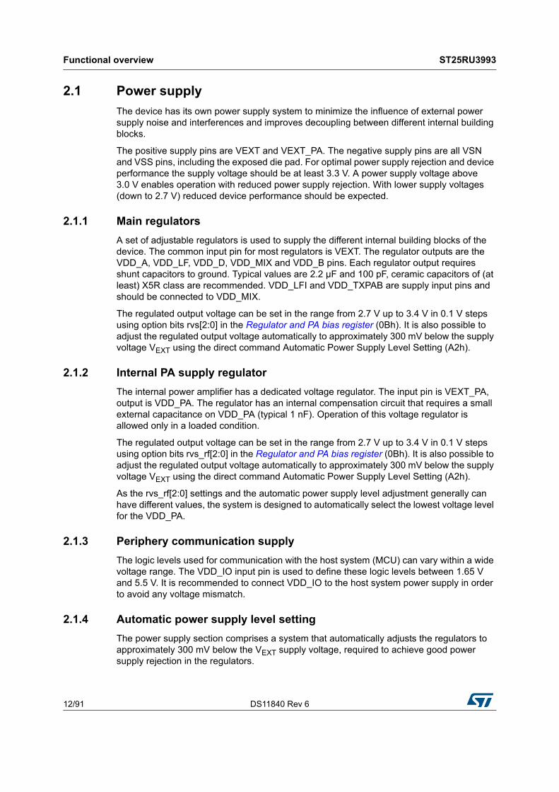
2.1 Power supply
The device has its own power supply system to minimize the influence of external power supply noise and interferences and improves decoupling between different internal building blocks.
The positive supply pins are VEXT and VEXT_PA. The negative supply pins are all VSN and VSS pins, including the exposed die pad. For optimal power supply rejection and device performance the supply voltage should be at least 3.3 V. A power supply voltage above 3.0 V enables operation with reduced power supply rejection. With lower supply voltages (down to 2.7 V) reduced device performance should be expected.
2.1.1 Main regulators
A set of adjustable regulators is used to supply the different internal building blocks of the device. The common input pin for most regulators is VEXT. The regulator outputs are the VDD_A, VDD_LF, VDD_D, VDD_MIX and VDD_B pins. Each regulator output requires shunt capacitors to ground. Typical values are 2.2 µF and 100 pF, ceramic capacitors of (at least) X5R class are recommended. VDD_LFI and VDD_TXPAB are supply input pins and should be connected to VDD_MIX.
The regulated output voltage can be set in the range from 2.7 V up to 3.4 V in 0.1 V steps using option bits rvs[2:0] in the Regulator and PA bias register (0Bh). It is also possible to adjust the regulated output voltage automatically to approximately 300 mV below the supply voltage VEXT using the direct command Automatic Power Supply Level Setting (A2h).
2.1.2 Internal PA supply regulator
The internal power amplifier has a dedicated voltage regulator. The input pin is VEXT_PA, output is VDD_PA. The regulator has an internal compensation circuit that requires a small external capacitance on VDD_PA (typical 1 nF). Operation of this voltage regulator is allowed only in a loaded condition.
The regulated output voltage can be set in the range from 2.7 V up to 3.4 V in 0.1 V steps using option bits rvs_rf[2:0] in the Regulator and PA bias register (0Bh). It is also possible to adjust the regulated output voltage automatically to approximately 300 mV below the supply voltage VEXT using the direct command Automatic Power Supply Level Setting (A2h).
As the rvs_rf[2:0] settings and the automatic power supply level adjustment generally can have different values, the system is designed to automatically select the lowest voltage level for the VDD_PA.
2.1.3 Periphery communication supply
The logic levels used for communication with the host system (MCU) can vary within a wide voltage range. The VDD_IO input pin is used to define these logic levels between 1.65 V and 5.5 V. It is recommended to connect VDD_IO to the host system power supply in order to avoid any voltage mismatch.
2.1.4 Automatic power supply level setting
The power supply section comprises a system that automatically adjusts the regulators to approximately 300 mV below the VEXT supply voltage, required to achieve good power supply rejection in the regulators.
DS11840 Rev 6 13/91
ST25RU3993 Functional overview
46
The direct command Automatic Power Supply Level Setting (A2h) activates the system. To switch back to manual power supply level adjustment, the direct command Manual Power Supply Level Setting (A3h) should be sent.
Before the direct command (A2h) is issued it is necessary to set and lock the PLL within the allowed target frequency (840 MHz to 960 MHz).
At the beginning of the automatic adjustment, the device sets the regulators to 3.4 V and enables the RF field to simulate a normal power supply load. During the procedure the device decreases the regulated voltage in 100 mV steps, each 300 µs long. The lowest voltage that the regulator can set is 2.7 V.
The procedure stops when the difference between the VEXT and the regulated voltages is at least 300 mV, or reaches the last step. The device then disables the RF field and sends an IRQ request with Irq_cmd bit (register 36h) set to high.
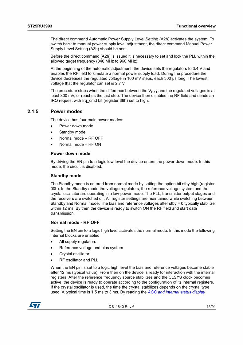
2.1.5 Power modes
The device has four main power modes:
• Power down mode
• Standby mode
• Normal mode – RF OFF
• Normal mode – RF ON
Power down mode
By driving the EN pin to a logic low level the device enters the power-down mode. In this mode, the circuit is disabled.
Standby mode
The Standby mode is entered from normal mode by setting the option bit stby high (register 00h). In the Standby mode the voltage regulators, the reference voltage system and the crystal oscillator are operating in a low-power mode. The PLL, transmitter output stages and the receivers are switched off. All register settings are maintained while switching between Standby and Normal mode. The bias and reference voltages after stby = 0 typically stabilize within 12 ms. By then the device is ready to switch ON the RF field and start data transmission.
Normal mode - RF OFF
Setting the EN pin to a logic high level activates the normal mode. In this mode the following internal blocks are enabled:
• All supply regulators
• Reference voltage and bias system
• Crystal oscillator
• RF oscillator and PLL
When the EN pin is set to a logic high level the bias and reference voltages become stable after 12 ms (typical value). From then on the device is ready for interaction with the internal registers. After the reference frequency source stabilizes and the CLSYS clock becomes active, the device is ready to operate according to the configuration of its internal registers. If the crystal oscillator is used, the time the crystal stabilizes depends on the crystal type used. A typical time is 1.5 ms to 3 ms. By reading the AGC and internal status display
Functional overview ST25RU3993
14/91 DS11840 Rev 6
register (2Ah), the MCU can check the crystal status. The status bit osc_ok = 1 in this register indicates that the crystal oscillation is stable and that the device is ready to operate.
If a continuously running TCXO is used the settling of the internal clock is faster, as only the OSCO pin DC level needs to be set. The same test with the osc_ok status bit as described above can be used.
After additional 500 ms (typ.) the device is ready to switch on the RF field and the transmission of inventory commands for transponder communication.
Normal mode - RF ON
By setting the rf_on option bit in the Device status control register (00h) the device immediately starts with the field ramp-up. The ramp-up time and shape are defined by trfon[1:0] and lin_mod option bits in the Modulator control register 3 (15h). When the RF field ramp-up is finished the rf_ok status bit (register 2Ah) is set to high. In addition an IRQ is generated, which is indicated by Irq_ana status bit set to high (register 38h).
Setting the option bit rf_on to low starts the field ramp-down. The RF field is decreased according to trfon[1:0] and lin_mod bits (register 15h). When this step is completed, the rf_ok status bit in AGC and internal status display register (2Ah) is set to low, and an IRQ is sent with the Irq_ana status bit high.
Table 1 summarizes the available power modes and the transitions times between them.
2.2 Host communication
A standard 4-wire serial interface (SPI) together with an interrupt request line (IRQ pin) is used to communicate with the device. An additional line (CLSYS) can be used as a system clock source for the MCU.
Table 1. Power modes overview
ModeEN
pin
Stby
option
bit
rf_on
option
bit
Current
consumption
Time to enter
the mode
Time from
mode to active RF field
Powerdown
L - - 1 μAImmediately from normal mode
12 - 17 ms (Crystal or TCXO start + bias start)
Standby H H L 3 mAImmediately from normal mode
12 - 17 ms (Crystal or TCXO start + bias start)
Normal H L L 24 mA12 - 17 ms (Crystal or TCXO start + bias start)
12.5 μs (Field ramp-up)
Normal with RF field on
H L H 75 mA12.5 μs (Field ramp-up)
NA
Table 2. Serial data interface (SPI interface) signal lines
Name SIgnal Signal level Description
NCS Digital input CMOS SPI enable (active low)
SCLK Digital input CMOS Serial clock
MOSI Digital input CMOS Serial data input
DS11840 Rev 6 15/91
ST25RU3993 Functional overview
46
By setting the NCS pin low the SPI interface is enabled. While NCS is high the SPI interface is deactivated. It is recommended to keep signal NCS high whenever the SPI interface is not used. MOSI is sampled at the falling edge of SCLK. The SPI communication is done in bytes. The first two bits of the first byte on the MOSI line (after NCS high-to-low) define the SPI operation mode. MSB bit is always transmitted first (valid for address and data).
The read and write modes support address auto incrementing for multi byte transfers. Only the first address needs to be sent and internally the address is incremented for consecutive reads or writes.
The MISO output is usually in tri-state and it is only driven when output data are available. This allows to short-circuit the MOSI and the MISO lines externally to create a bi-directional signal (see Figure 3).
During the time the MISO output is in high impedance it is possible to activate a 50 kΩ pull-down resistor by setting option bits miso_pd1 and miso_pd2 in Miscellaneous register 1 (0Dh).
Figure 3 shows the possible SPI interconnection options.
Figure 3. Possible SPI configurations
MISODigital output with tri-
stateCMOS Serial data output
IRQ Digital output CMOS Interrupt request output
CLSYS Digital output CMOS MCU clock output
Table 2. Serial data interface (SPI interface) signal lines (continued)
Name SIgnal Signal level Description
Functional overview ST25RU3993
16/91 DS11840 Rev 6
2.2.1 Writing to registers
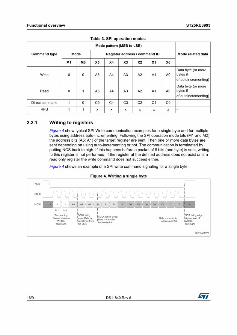
Figure 4 show typical SPI Write communication examples for a single byte and for multiple bytes using address auto-incrementing. Following the SPI operation mode bits (M1 and M2) the address bits (A5: A1) of the target register are sent. Then one or more data bytes are sent depending on using auto-incrementing or not. The communication is terminated by putting NCS back to high. If this happens before a packet of 8 bits (one byte) is sent, writing to this register is not performed. If the register at the defined address does not exist or is a read only register the write command does not succeed either.
Figure 4 shows an example of a SPI write command signaling for a single byte.
Figure 4. Writing a single byte
Table 3. SPI operation modes
Command type
Mode pattern (MSB to LSB)
Mode related dataMode Register address / command ID
M1 M0 X5 X4 X3 X2 X1 X0
Write 0 0 A5 A4 A3 A2 A1 A0Data byte (or more bytes if
of autoincrementing)
Read 0 1 A5 A4 A3 A2 A1 A0Data byte (or more bytes if
of autoincrementing)
Direct command 1 0 C5 C4 C3 C2 C1 C0 -
RFU 1 1 x x x x x x -
DS11840 Rev 6 17/91
ST25RU3993 Functional overview
46
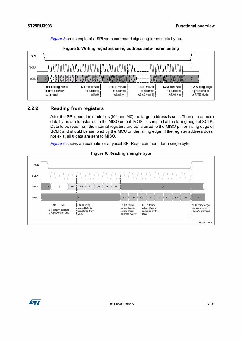
Figure 5 an example of a SPI write command signaling for multiple bytes.
Figure 5. Writing registers using address auto-incrementing
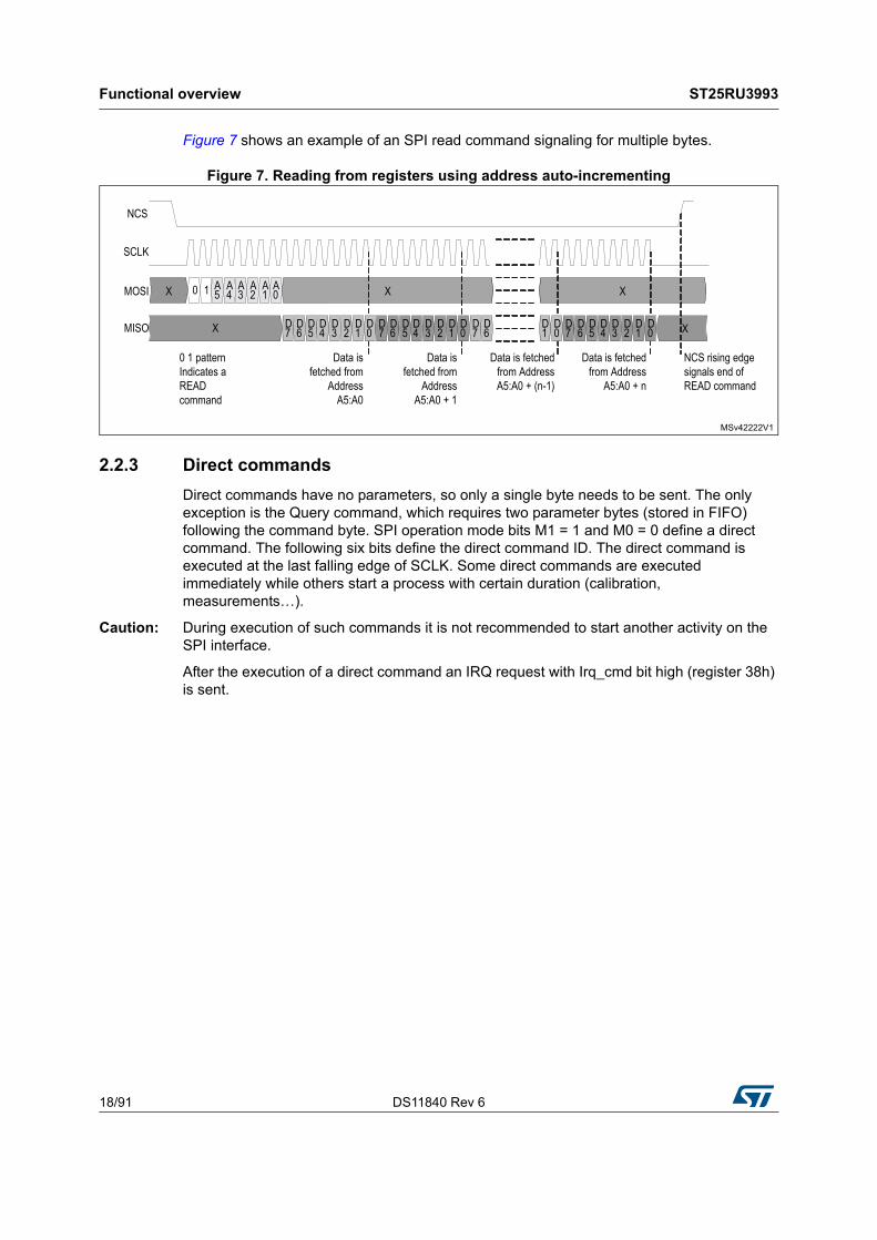
2.2.2 Reading from registers
After the SPI operation mode bits (M1 and M0) the target address is sent. Then one or more data bytes are transferred to the MISO output. MOSI is sampled at the falling edge of SCLK. Data to be read from the internal registers are transferred to the MISO pin on rising edge of SCLK and should be sampled by the MCU on the falling edge. If the register address does not exist all 0 data are sent to MISO.
Figure 6 shows an example for a typical SPI Read command for a single byte.
Figure 6. Reading a single byte
Functional overview ST25RU3993
18/91 DS11840 Rev 6
Figure 7 shows an example of an SPI read command signaling for multiple bytes.
Figure 7. Reading from registers using address auto-incrementing
2.2.3 Direct commands
Direct commands have no parameters, so only a single byte needs to be sent. The only exception is the Query command, which requires two parameter bytes (stored in FIFO) following the command byte. SPI operation mode bits M1 = 1 and M0 = 0 define a direct command. The following six bits define the direct command ID. The direct command is executed at the last falling edge of SCLK. Some direct commands are executed immediately while others start a process with certain duration (calibration, measurements…).
Caution: During execution of such commands it is not recommended to start another activity on the SPI interface.
After the execution of a direct command an IRQ request with Irq_cmd bit high (register 38h) is sent.

DS11840 Rev 6 19/91
ST25RU3993 Functional overview
46
Direct command description
The direct commands supported by the ST25RU3993 are detailed below. Values in parentheses show the related command byte.
Table 4. List of direct commands
Code (HEX) Command Direct execution
80h Idle Yes
81h Direct Mode Yes
83h Soft Init Yes
84h Hop to Main Frequency Yes
85h Hop to Auxiliary Frequency Yes
87h Trigger AD Conversion No
88h Trigger Rx Filter Calibration No
89h Decrease Rx Filter Calibration Data Yes
8Ah Increase Rx Filter Calibration Data Yes
90h Transmission with CRC Yes
91h Transmission with CRC Expecting Header Bit Yes
92h Transmission without CRC Yes
96h Block Rx Yes
97h Enable Rx Yes
98h Query Yes
99h QueryRep Yes
9Ah QueryAdjustUp Yes
9Bh QueryAdjustNic Yes
9Ch QueryAdjustDown Yes
9Dh ACK Yes
9Fh ReqRN Yes
A2h Automatic power supply level setting No
A3h Manual power supply level setting Yes
A4h Automatic VCO range selection No
A5h Manual VCO range selection Yes
A6h AGL On Yes
A7h AGL Off Yes
A8h Store RSSI Yes
A9h Clear RSSI Yes
AAh Interrogator anti-collision support enable Yes
ABh Interrogator anti-collision support disable Yes

Functional overview ST25RU3993
20/91 DS11840 Rev 6
• Direct mode (81h): device enters the direct mode.
• Soft init (83h): this command resets the configuration registers to their default values and terminates all functions that were triggered before.
• Hop to main frequency (84h): this command forces the PLL to use the frequency defined in the PLL Main Registers 1 - 3. The PLL main registers are used per default.
• Hop to auxiliary frequency (85h): This command forces the PLL to use the frequency setting defined in the PLL auxiliary register 1, PLL auxiliary register 2 and PLL auxiliary register 3.
• Trigger A/D conversion (87h): this command triggers the analog to digital conversion using the internal 8-bit A/D converter. For further information, refer to the A/D Converter description.
• Trigger Rx filter calibration (88h): this command triggers the Rx filter calibration procedure. For further information, refer to the Rx filter calibration description.
• Decrease Rx filter calibration data (89h), Increase Rx filter calibration data (8Ah): these commands adjust the automatically acquired Rx filter calibration data. For further information, refer to the Rx filter calibration description.
• Transmission with CRC (90h): transmission commands are used to transmit data from the reader to transponders. First, the Tx length registers (3Dh, 3Eh) need to be set with the number of complete bytes for transmission, including the number of bits for the incomplete byte. Then transmission data can be loaded in the FIFO register (3Fh). Transmission starts when the first byte is loaded. CRC-16 is included in the transmitted sequence. The optimal way to load all transmission data is to use the Continuous Write mode, starting with the address 3Dh. Example Using Address Auto-Incrementing: SPI data (MOSI): 90h - 3Dh - 00h - 30h - AAh - BBh - CCh operates as follows:
– 90h:Transmission with CRC
– Write 00h to 3Dh
– Write 30h to 3Eh (three bytes are going to be transmitted)
– Write AAh, BBh, CCh to address 3Fh (FIFO data which will be transmitted).
• Transmission with CRC expecting header bit (91h): same as the previous command, but it also informs Rx decoding logic that an header bit is expected in the response.
• Transmission without CRC (92h): same as direct command ‘Transmission with CRC’, but the CRC part is omitted.
• Block Rx (96h): the Block Rx command deactivates the digital part of receiver (bit decoder and framer). Turning OFF the receiver is useful if the system operates in a noisy environment, causing a constant switching of the sub-carrier input of the Rx digital part. The active receiver will try to detect a Preamble and if the noise pattern matches the expected signal pattern, an interrupt is generated. A constant flow of interrupt requests can be a problem for the MCU, Such situation can be avoided by deactivating the receive decoder using the Block RX command. The receiver is automatically reactivated at the end of any data transmission after the Rx wait time elapses. To set the Rx wait time refer to the Rx Wait Timer section. A second possibility to stop Block Rx is to send the Enable Rx (97h) command.
• Enable Rx (97h): this command prepares analog and digital part of the receiver for reception. This command should be sent to trigger the reception manually. This
DS11840 Rev 6 21/91
ST25RU3993 Functional overview
46
command should not be sent if reception is automatically triggered by a data transmission command.
• Query (98h): the Query command issues the EPC Query, which starts the inventory round. The Query command requires additional two data bytes which should be written to the FIFO (3Fh): The two bytes in the FIFO should contain: “00”, DR, M, TRext, Sel, Session, Target, Q Since this adds-up to 15 applicable bits, the LSB bit is disregarded. The transmitter in the end sends:
– Preamble
– Command ID
– Tx data (two bytes from FIFO)
– CRC-5.
The received RN16 is stored in the internal RN16 register for further communication steps (ACK, ReqRN). RN16 is also stored in the FIFO.
• QueryRep (99h): the QueryRep command issues the EPC Gen2 QueryRep command followed by two session bits. The session bits are taken from Tx setting register (3Ch). The received RN16 is stored in the internal RN16 register for further communications (ACK, ReqRN). RN16 is also accessible in the FIFO.
• QueryAdjustUp (9Ah): the QueryAdjustUp direct command issues the EPC Gen2 QueryAdjust command followed by two session bits and ‘up’ parameter (increasing the number of available slots). The session bits are taken from Tx setting register (3Ch). The received RN16 is stored in the internal RN16 register for further communications (ACK, ReqRN). RN16 is also accessible in the FIFO.
• QueryAdjustNic (9Bh): the QueryAdjustNic command issues the EPC Gen2 QueryAdjust command followed by two session bits and ‘no change’ parameter. The session bits are taken from Tx setting register (3Ch). The received RN16 is stored in the internal RN16 register for further communications (ACK, ReqRN). RN16 is also accessible in the FIFO.
• QueryAdjustDown (9Ch): the QueryAdjustUp command issues the EPC Gen2 QueryAdjust followed by two session bits and ‘down’ parameter (decreasing the number of available slots). The session bits are taken from Tx setting register(3Ch). The received RN16 is stored in the internal RN16 register for further communications (ACK, ReqRN). RN16 is also accessible in the FIFO.
• ACK (9Dh): the ACK command issues the EPC ACK followed by RN16 stored in the internal RN16 register during last successful Query command.
• NAK (9Eh): the NAK command issues the EPC Gen2 NAK command to tags.
• ReqRN (9Fh): the ReqRN command issues the EPC Request RN to the tag. The last received RN is used as a parameter and the received new RN16 (handle) is stored in the internal RN16 register for further communications (ACK, ReqRN). New RN16 is also stored in the FIFO.
• Automatic power supply level setting (A2h), manual power supply level setting (A3h): these commands trigger the automatic adjustment of the on-board voltage

Functional overview ST25RU3993
22/91 DS11840 Rev 6
regulators, and switch back to the manual selection. See Periphery Communication Supply description for more details.
• Automatic VCO range selection (A4h), manual VCO range selection (A5h): these commands trigger the automatic VCO range selection and switch back to manual VCO range selection. See PLL and VCO description for more details.
• AGL on (A6h), AGL off (A7h): these commands trigger and disable the AGL action. See AGL description for more details.
• Store RSSI (A8h), Clear RSSI (A9h): these commands store and clear the received signal strength indicator (RSSI) data that can be used for IQ decision circuitry. See IQ Selection description for more details.
• Interrogator anti-collision support enable (AAh), interrogator anti-collision support disable (ABh): these commands enable or disable the interrogator anti-collision support defined in ISO 29143.
Direct command chaining
Direct commands with immediate execution can be followed by another SPI commands like Read or Write without deactivating the NCS signal in between.
Figure 8. Sending direct commands
2.2.4 SPI interface timing
Table 5. SPI timing parameters
Symbol Parameter Note/Condition Min Typ Max Unit
General (VDD_IO > 3 V, CLOAD < 50 pF, hs_output = 1)
BRSPI Bit rate - - - 5 Mbps
tSCLKH Clock high time - 70 - - ns
tSCLKL Clock low time - 70 - - ns
tNCSL NCS setup time
Time between NCS high-low transition to first SCLK high transition
10 - - ns

DS11840 Rev 6 23/91
ST25RU3993 Functional overview
46
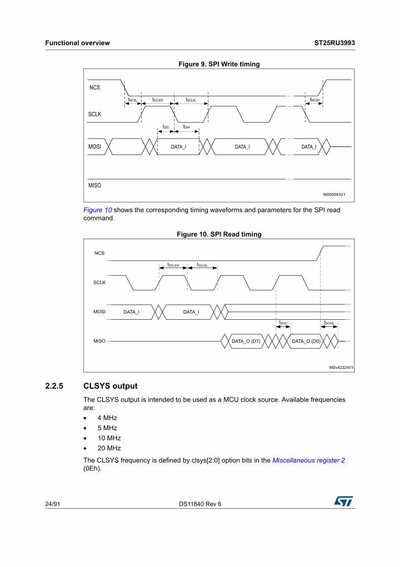
Figure 9 shows the corresponding timing waveforms and parameters for the SPI write
command.
tDISData-in setup
time- 10 - - ns
tDIH Data-in hold time - 10 - - ns
tNCSHNCS hold time Read / Write
Time between last SCLK falling edge and NCS low-high transition after a Read or Write
10 - - ns
tNCSHNCS hold time
direct command
Time between last SCLK falling edge and NCS low-high transition after a direct command
70 - - ns
Read timing
tDOD Data out delay
VDD_IO ≥ 3 V,
CLOAD = 50 pF,
hs_output = 1
- 30 - ns
tDOD Data out delay
VDD_IO ≥ 1.65 V,
CLOAD = 50 pF,
hs_output = 1
- 60 - ns
tDOD Data out delay
VDD_IO ≥ 3 V,
CLOAD = 50 pF,
hs_output = 0
- 90 - ns
tDOHZData out to high impedance delay
Time for the SPI to release the MISO line
- 40 - ns
Table 5. SPI timing parameters (continued)
Symbol Parameter Note/Condition Min Typ Max Unit
Functional overview ST25RU3993
24/91 DS11840 Rev 6
Figure 9. SPI Write timing
Figure 10 shows the corresponding timing waveforms and parameters for the SPI read command.
Figure 10. SPI Read timing
2.2.5 CLSYS output
The CLSYS output is intended to be used as a MCU clock source. Available frequencies are:
• 4 MHz
• 5 MHz
• 10 MHz
• 20 MHz
The CLSYS frequency is defined by clsys[2:0] option bits in the Miscellaneous register 2 (0Eh).

DS11840 Rev 6 25/91
ST25RU3993 Functional overview
46
2.2.6 IO signal level and output characteristics
The logic high level for the host communication and CLSYS is defined by the supply voltage connected to VDD_IO pin. The logic high level can be in the range between 1.65 V and 5.5 V. VDD_IO should be connected to the host system periphery supply voltage to ensure matching communication levels.
The digital outputs are by default configured for high-speed operation. A 5 MHz SPI clock is possible with a 50 pF capacitive load on the MISO and IRQ outputs and a minimum VDD_IO supply voltage of 3 V. A 3 MHz SPI clock is possible with a 50 pF load and a minimum VDD_IO supply voltage of 1.65V.
To decrease the harmonic content of the digital output signals, it is possible to configure the device outputs to provide weak, sloped output signals by setting the hs_output option bit in the Miscellaneous register 1 (0Dh) to low. In this configuration the possibility of interferences by the host system communication with other internal building blocks of the device is mitigated as well. Using this option a 2 MHz SPI clock is possible with maximum 50 pF capacitive load on MISO and IRQ and at least a VDD_IO supply voltage of 3 V.
It is also possible to define open drain N-MOS outputs by setting the option bit open_dr high (register 0Dh). This option reduces the harmonic content on the MISO, IRQ, and CLSYS signals further. It also decreases cross-coupling effects that could interfere with operation of other blocks of the device.
2.2.7 OAD, OAD2 outputs
The OAD and OAD2 outputs are analog and digital test outputs. When used as analog outputs, the received sub-carrier signals or mixer analog DC output levels are multiplexed at these pins. The signal is centered to AGD level. When used as digital output, the levels are configured with VDD_IO. The OAD pins can be configured as high speed outputs by setting the option bit hs_oad in the Miscellaneous register 1 (0Dh). During normal operation it is not recommended to use hs_oad, as higher harmonic content can increase the crosstalk to sensitive pins of the device.
2.3 PLL and VCO section
The PLL section comprises a voltage controlled oscillator, a pre-scaler, main and reference dividers, a phase-frequency detector, a charge pump and a loop filter.
Figure 11 shows a detailed block diagram of the PLL and VCO section of the ST25RU3993 device.

Functional overview ST25RU3993
26/91 DS11840 Rev 6
Figure 11. PLL and VCO section
All building blocks, except a section of the loop filter, are integrated in the ST25RU3993.The allowed frequency operation range is 840 MHz to 960 MHz.
2.3.1 Voltage controlled oscillator
The VCO is entirely integrated, including the variable capacitor and inductor. The frequency control input pin is LF_CEXT. The valid voltage range is between 0.5 V and VDD_A - 0.5 V. The option bits eosc[2:0] in the VCO control register (11h) are used for oscillator noise and current consumption optimization. Power supply decoupling is done via VOSC pin. The internal VCO frequency is set in the range of 1800 MHz, which is internally divided by two for decreased VCO pulling effect. The tuning curve of the 1800 MHz VCO is divided into 16 segments (ranges) to decrease the VCO gain and to attain lowest possible phase noise.
VCO tuning range selection
The selection of the VCO tuning range can be done manually by setting the option bits vco_r[3:0] in the VCO control register(11h). An automatic selection can be started by using the direct command Automatic VCO Range Selection (A4h). Reverting back to manual selection is possible by sending the direct command Manual VCO Range Selection (A5h). The Automatic VCO Range Selection (A4h) command starts a search algorithm that finds the appropriate VCO segment. When the algorithm is finished an IRQ request is sent with Irq_cmd and autovco_done status bit in the Command status display register (2Eh) set high.

DS11840 Rev 6 27/91
ST25RU3993 Functional overview
46
Readout of VCO tuning range status
The result of the automatic segment search algorithm is represented by vco_ri[7:4], which can be read out from the device via the AGL/VCO/F_CAL/PilotFreq status register (r2Cpage[1:0] = 01) (2Ch) when option bits r2Cpage[1:0] = 01b (register 29h).
VCO control voltage measurement
It is possible to measure the VCO control voltage by setting option bit mvco in VCO control register (11h) to high. The 3 bits result vco_ri[2:0] can be read from the AGL/VCO/F_CAL/PilotFreq status register (r2Cpage[1:0] = 01) (2Ch) using r2Cpage[1:0] = 01b (register 29h). During normal operation, the mvco option bit in register 11h should remain low. Details on using the 1800 MHz VCO are described in a dedicated application note.
2.3.2 PLL prescaler and main divider
The divide-by-32/33 prescaler is controlled by the N-divider. The divider ratio is defined by the PLL main register 1 and PLL main register 3 (17h-19h) or PLL auxiliary register 1 and PLL auxiliary register 3 (1Ah-1Ch). The lower ten bits of the three main (aux.) registers define the A value and the next upper ten bits define the B value. The A and B values define the main divider dividing ratio to:
The two registers PLL main register 1 and PLL main register 3 and PLL auxiliary register 1 and PLL auxiliary register 3 are intended to support frequency hopping using the direct commands Hop to Main Frequency (84h) and Hop to Auxiliary Frequency (85h).
2.3.3 PLL reference frequency
The reference frequency is selected by the RefFreq[2:0] bits in the PLL main register 1 (17h). Available values are:
• 125 kHz
• 100 kHz
• 50 kHz
• 25 kHz
2.3.4 Reference frequency source
For the reference frequency a frequency source of 20 MHz is required. It is possible to use an external oscillator (TCXO) or a quartz crystal. If a TCXO is used, it should be connected to the OSCO pin while the OSCI pin should be shorted to ground. The signal shape of the TCXO should be of a sinusoidal type and AC coupled. The level should be in the range between 0.8 Vpp and 3 Vpp. A low OSCO level is recommended to minimize the spectral signal components spaced by ±20 MHz around the Tx carrier frequency. The OSCO input impedance in this mode is typically 9 kΩ, with 9 pF in parallel. A crystal should be connected between the OSCI and OSCO pins with appropriate load capacitors in shunt configuration to ground. Load capacitances in the range from 15 pF to 20 pF are recommended. The maximum series resistance in resonance should be 30 Ω. The crystal oscillator is started-up in fast mode in order to speed-up a stable crystal oscillation. The device then switches back to the power saving mode. The device operation typically uses the power saving mode.
N B 32⋅ A 33⋅+=
Functional overview ST25RU3993
28/91 DS11840 Rev 6
Option bits xosc[1:0] in the Miscellaneous register 2 (0Eh) are available to manually control the crystal operation modes.
2.3.5 Phase-frequency detector and charge pump
The reference frequency and the divided RF frequency are compared in the phase-frequency detector that drives the charge pump connected to the LF_CEXT pin. The charge pump current is selectable between 150 µA and 2350 µA using option bits cp[2:0] in the CP control register (12h).
2.3.6 Loop filter
The loop filter is composed of an external and an internal portion. The first stage (series capacitor, series resistor and shunt capacitor) is external and is connected to the pin LF_CEXT. The second stage (R3/C3 filter) is internally connected between the LF_CEXT pin and the VCO control input.
The values for the internal part of the loop filter (R3 and C3) can be selected by option bits LF_R3[7:6] and LF_C3[5:3] both in the CP Control Register (12h). R3 can be set in a range from 30 kΩ to 100 kΩ and C3 can be set in a range from 20 pF to 200 pF.
2.3.7 Frequency hopping commands
Frequency hopping is possible by issuing the direct commands Hop to Main Frequency (84h) and Hop to Auxiliary Frequency (85h) that set the main divider ratio either to the main or the auxiliary PLL register. The host system (MCU) is responsible to perform correct frequency hopping according to local regulations.
2.3.8 PLL start-up and frequency hopping
Before enabling the RF field, the host system needs to configure the PLL through the CP control register (12h) and the PLL main register 1, PLL main register 2 and PLL main register 3 (17h, 18h, 19h). The PLL should be locked using one of the above defined possibilities. Any time during operating at one frequency, the host system can fill the auxiliary PLL Main Registers. When the frequency hop needs to be performed only the appropriate frequency hopping direct command needs to be sent to the device.
2.4 Device status control
In the Device status control register (00h), the main functionality of the device is controlled. By setting the option bit rf_on, the internal transmitter and receiver blocks are enabled. The initial RF field ramp-up is defined by the Tari[2:0] option bits in the Tx options register (02h) and by option bits trfon[1:0] in the Modulator control register 3(15h).
The available values are:
• 100 µs
• 200 µs
• 400 µs
• TARI determined
When finished, the rf_ok bit in the AGC and internal status display register (2Ah) is set and an IRQ with Irq_ana bit is sent. By setting the rf_on bit low, the RF field is ramped-down

DS11840 Rev 6 29/91
ST25RU3993 Functional overview
46
similarly to the ramp-up transient and an IRQ with Irq_ana bit set is sent. The rec_on bit enables the receiver only. The agc_on bit enables the AGC functionality. The stby bit puts the device into the standby mode.
2.5 Protocol control
In the Protocol selection register (01h), the main protocol parameters are selected. The prot[2:0] option bits should be set to 000b for EPC Class1 Gen2 operation and to 001b for ISO18000-6A/B FM0 decoder operation. The AutoACK[1:0] bits enables the automatic inventory round sequencing and define its depth. There are three possible modes:
• No automatic
• Automatic ACK
• Automatic ACK + ReqRN
The option bit RX_crc_n = 1 defines reception with no internal CRC check. The CRC is then just passed on to the FIFO like any other data bytes. In the EPC Gen 2 protocol this is a useful feature in case of a truncated EPC reply, where the stored CRC that a transponder transmits is not calculated over the actual transmitted data and is therefore an invalid CRC. The dir_mode bit defines the type of output signals while operating in the direct mode. It also disables any decoding and signal sensing automatics during the reception. It is advised to set this bit high when continuous analog measurements are performed.
2.6 Transmission section
The transmitter section comprises a data handling, an encoding part, a shaping circuitry, a modulator and amplifier circuitry.

Functional overview ST25RU3993
30/91 DS11840 Rev 6
Figure 12. Transmission section
The RF carrier is modulated with a shaped representation of the transmit data and (pre-)amplified for transmission.
2.6.1 Tx data handling and coding
The data handling part takes the baseband data from the FIFO and encodes it according to the Gen2 protocol (PIE). It adds a preamble or a frame-sync and calculates the CRC. The digital modulation signals are fed to the shape circuitry.
2.6.2 Tx shape circuitry
The modulation shape is controlled by a double D/A converter. The first 5-bit logarithmic converter creates two voltages, which define minimum and maximum (Vpp) modulation signal level. The two voltages are filtered by two external capacitors connected to the CD1 and CD2 pins to minimize the noise level and are used as a reference for the shaping circuitry. The second 9-bit linear converter transforms the digital modulation signal into a sinusoidal or linear shaped analog modulation signal. The output of the shaping circuit is interpolated and connected to the modulator input.
2.6.3 Local oscillator (LO) path
To improve the phase noise rejection, the local oscillator signal is derived from the output of the pre-amplifier stages. For optimal operation, the pre-amplifier levels should be close to
DS11840 Rev 6 31/91
ST25RU3993 Functional overview
46
nominal (set by TX_lev[4:0] in register 15h). If lower levels are used, the LO signal can be increased by approximately 6 dB using option bit eTX[7]. The drawback is increased received noise.
2.6.4 Modulator
The modulator modulates the RF carrier with the shaped representation of the digital modulation signal. The internal modulator is capable of ASK and PR-ASK modulation.
Tx level and shape adjustments
The output level and modulation shape properties are controlled by the Modulator control register 1 and Modulator control register 4 (13h-16h). The level of the output signal is adjusted by option bits TX_lev[4:0] in Modulator control register 3(15h). For good performance, it is advised to design the external circuit of the reader device to have the reader output power close to the ST25RU3993 nominal output power. If temporarily operation at decreased power is need the TX_lev[4:0] option bits should be used.
Sinusoidal or linear shape is defined by the option bit lin_mod in register (15h). PR-ASK modulation is selected by setting the pr_ask option bit to high. If PR-ASK is selected, the del_len[5:0] option bits are used to adjust the delimiter length in the range from 9.6 µs to 15.9 µs. For Tari = 25 µs PR-ASK and ASK delimiter shapes are available. The ASK transient which gives more accurate timing can be selected by the ook_ask option bit in register 15h. For Tari = 12.5 µs and 6.25 µs only the ASK delimiter shape is available.
ASK modulation is selected by setting the pr_ask option bit to low. In ASK modulation it is possible to adjust the delimiter length by setting the option bit ook_ask. In this case, ook_ask defines 100% ASK modulation and the del_len[5:0] bits are used for delimiter length setting as in the PR-ASK mode described above.
The rate of the modulation transient is automatically adjusted to the selected Tari setting and can be re-adjusted by the ask_rate[1:0] option bits (register 13h). For smoother transitions of the modulation signal an optional low pass filter can be activated by the e_lpf option bit in the Modulator control register 1 (13h). Bits aux_mod and main_mod define whether the modulation signal will be connected to the low-power output or to the internal PA output path. If one of the outputs is enabled by the eTX[3:0] bits in RF output and LO control register (0Ch) and corresponding aux_mod or main_mod bit is low, the output is enabled but not modulated (the device would output only a continuous wave signal).
2.7 Tx outputs
Two Tx differential output ports are available:
• Differential low-power, high linear output (nom. 0 dBm)
• Differential high power output (nom. 20 dBm)
The low-power output can be used to drive an external PA to generate a high power RF signal. The internal high power output can be used to directly drive an antenna suitable for applications with low to medium read range requirements.
low-power output
The differential low-power, high linear RF outputs (~0 dBm) are intended to be used to drive an external amplifier. The RF outputs composed of RFOPX and RFONX pins need external RF chokes connected to VDD_B, decoupling capacitors and a Balun with 2:1 impedance

Functional overview ST25RU3993
32/91 DS11840 Rev 6
ratio for optimal operation in a 50 Ω system. The output is enabled by eTX[1:0] bits in the RF Output and LO Control Register (0Ch). By using these bits, it is possible to adjust current capability of the RF output pins.
High power output
The differential high power output pins are the outputs of the internal power amplifier outputs PAOUT_P and PAOUT_N. They require external RF chokes, connected to VDD_PA and an impedance matching circuit for operation in a 50 Ω system. The amplifier is enabled by the eTX[4] and eTX[3:2] option bits in register 0Ch. Bit eTX[3:2] also define the bias of the internal pre-amplifier stage. The PA supply regulator is automatically enabled when the internal PA is enabled. The bias current for the internal PA is defined by the option bits pa_bias[1:0] in the Regulator and PA bias register (0Bh).
2.8 Tx operation modes
2.8.1 TX normal mode
The baseband data is transferred to the 24 byte FIFO and the complete signal processing (protocol encoding, adding preamble or frame-sync, CRC, signal shaping, and modulation) is done internally. The data is then coded to the modulation pulse level and sent to the modulator. This means that the MCU has only to load the FIFO with data.
Transmission start
There are three possibilities to start data transmission in the normal mode.
The first one is data transmission that can be triggered by sending related direct commands:
• Transmission with CRC (90h)
• Transmission with CRC Expecting Header Bit (91h)
• Transmission without CRC (92h)
followed by information about the number of bytes that should be transmitted and the baseband data. The number of bytes that needs to be written into the Tx length register 1 and Tx length register 2 (3Dh, 3Eh) and the data itself should be put into the FIFO I/O register (3Fh). Both operations can be done with one continuous Write command. The transmission is started when the first data byte is completely written to the FIFO.
The second possibility to trigger the transmission is with one of the direct commands related to the EPC Class1 Gen2 protocol:
• Inventory Commands:
– Query (98h)
– QueryRep (99h)
– QueryAdjustUp (9Ah)
– QueryAdjustNic (9Bh)
– QueryAdjustDown (9Ch)
• ACK (9Dh)
• ReqRN (9Fh)
In this case, the transmission is started upon receiving the command.
DS11840 Rev 6 33/91
ST25RU3993 Functional overview
46
The third possibility for data transmission is using one of the AutoACK modes. In this case the ACK or ReqRn is sent automatically if the previous reception was successful.
During data transmission, the TX_status bit in the FIFO status register (39h) is set. When the data transmission is finished, the reader device signals an IRQ request with Irq_TX bit set high.
Protocol adjustments
The EPC Class1 Gen 2 protocol allows the user to adjust transmission parameters. The three supported Tari values are selected by changing the Tari[1:0] option bits in the Tx options register (02h). The length of the high period of the (PIE encoded) logical one is selected by TXOne[1:0] option bits in the Tx options register (02h). The session parameters for the direct command Query (98h) are defined by the S1 and S0 option bits in the Tx setting register (3Ch). TRcal, which defines the backscatter link frequency, is incorporated in the Query command transmission. TRcal is defined by option bits TRcal[11:0] in the TRcal Registers (04h, 05h).
Caution: The software designer needs to take care that bits TRcal[11:0], RX_LF[3:0] and the DR bit in the transmission of the Query command follow the Gen2 protocol. A precise description can be found in the EPC Class1 Gen2 or ISO18000-6C protocol description. If TRcal data is required in normal transmission, it can be set by Force_TRcal option bit in the Tx setting register (3Ch). The cyclic redundancy check can be changed to CRC-5 instead of CRC-16. This is done in normal transmission by setting TXCRC_5 option bit in the Tx setting register (3Ch) to high.
Transmission FIFO
The reader device supports two fully separate 24-byte FIFO buffer registers, one for transmission and one for reception. They share the same address. By writing to FIFO address 3Fh the data will be passed to transmission FIFO, while reading from the register address 3Fh will fetch the values from the reception FIFO. This approach makes it possible to start a new transmission before the previously received data is read out by the MCU.
If the data bytes to transmit exceed the size of the FIFO buffer, the MCU should initially fill the FIFO register with 24 bytes. The reader device starts the transmission and sends an interrupt request, signaled by irq_fifo in the Interrupt register 1 (37h), when only 6 bytes are left in the FIFO. When the interrupt is received, the MCU needs to read from register 37h. By reading this register, the host system will know the cause for the interrupt and at the same time clear the interrupt bit. After this the MCU puts the remaining transmission data bytes to the FIFO considering the available FIFO size. If all transmission data bytes were already sent to the FIFO, the host system waits until the last data byte has been sent. The end of the transmission is signaled to the MCU by the IRQ request irq_TX in register 37h. The two Tx length register 1 and Tx length register 2 (3Dh, 3Eh) support incomplete byte transmission. The MCU needs to define the number of complete bytes and the number of the remaining bits that should be transmitted.
2.8.2 TX direct mode
Direct mode is chosen when using only analog functions, bypassing all the protocol handling support of the reader device.

Functional overview ST25RU3993
34/91 DS11840 Rev 6
Entering and terminating the Direct Mode
To enter the direct mode the direct command Direct Mode (81h) should be sent followed by a NCS low-to-high transition. The direct mode remains active as long as NCS is kept high. To terminate the direct mode the direct command Block Rx (96h) needs to be sent immediately after the NCS high-to-low transition. During the same or consecutive NCS low periods normal communication via the SPI interface is possible again.
Direct Mode Signals
The Table 6 shows the re-assignments of the I/O pins during the direct mode. The different reception outputs options are related to the dir_mode option bit in the Protocol selection register (01h).
In the direct mode the MCU must directly control the transmission modulation input pin MOSI (Tx data input). The RF field is set to a high level if MOSI is high and to low if MOSI is low. The circuitry shapes the field according to the settings in the Modulator control register 1 and Modulator control register 3 (13h-15h) and transmits the signal.
2.9 Receiver
The receiver section comprises two input mixers followed by a fast AC coupling, gain and filtering stages, and a digitizer. The two received signals are fed to the decision circuitry, the bit-decoder and the framer, where the preamble is removed and CRC is checked. The clean, framed baseband data is accessible for the MCU via the 24-byte FIFO I/O register (3Fh).
The receiver section is activated by the option bits rec_on or rf_on from the Device status control register (00h). The typical bias settling time is 3 ms if the reader device was previously in the normal mode (EN=H and stby=0). If the rec_on bit is set together with the EN pin or a stby high-low change, the normal mode power-up timing prevails.
Figure 13 shows a detailed block diagram of the receiver section of the ST25RU3993 device.
Table 6. I/O pin reassignment in direct mode
Pin NameBit Stream and Bit Clock Output
(dir_mode = 0)Sub Carrier Output
(dir_mode = 1)
MOSI Tx data input Tx data input
SCLK Enable Rx input Enable Rx input
MISO Rx data output I-Channel subcarrier output
IRQ Rx bit clock output Q-Channel subcarrier output

DS11840 Rev 6 35/91
ST25RU3993 Functional overview
46
Figure 13. Receiver section
2.9.1 Input mixers
The two input mixers are driven with 90° shifted LO signals and form an IQ demodulation circuit. By using an IQ demodulator architecture the AM-input signals are demodulated in the in-phase channel (I) while the PM-input signals are demodulated in the quadrature phase (Q) channel. The mixture of AM and PM-input signals is demodulated in both receiving channels. This configuration results in reliable operation, even if the transponder presents amplitude or phase modulation at receiver’s input, as it suppresses communication holes caused by alternating modulation types. A differential input mixer and a single ended input mixer are available.
Differential input mixer
The pins MIX_INP and MIX_INN are the inputs for the differential Rx mixer. The inputs should be AC coupled to the external circuitry. At power-up the device automatically chooses the differential Rx mixer. If the differential Rx mixer is not used the input pins should be shorted to ground. To optimize the receiver noise and input range properties, the differential Rx mixer features settings to adjust the input range. Depending on the reflectivity of the environment and the antenna properties, the receiver’s input RF voltage may increase to a level at which the differential Rx mixer operation gets corrupted. In such a case the input range can be extended by activating the internal input attenuator by setting the option bit mix_ir[0] in theRx mixer and gain register (0Ah) to high. If of low unwanted
Functional overview ST25RU3993
36/91 DS11840 Rev 6
reflected power (self-jammer), the host system can increase the mixer conversion gain improving the overall sensitivity of the receiver by setting the option bit mix_ir[1]. The drawback of this setting is a reduced dynamic input range.
Additional settings in Emitter-coupled mixer options register (22h):
• emix_vr[0]: (i2x) Increase differential Rx mixer range in mixer gain mode (~3dB)
• emix_vr[1]: (vsp_low) Adapts differential Rx mixer bias points to low supply
• iadd_sink[2:0]: Select differential Rx mixer load stage
Single ended input mixers
The single ended input mixer has emitter-coupled input topology. The input MIXS_IN pin should have a DC path to ground and should be AC coupled for the RF input signal. The single ended input mixer needs to be activated by s_mix bit in the Miscellaneous register 1 (0Dh).
Following options are available to optimize mixer operation for different mixer input ranges, sensitivity and current consumption requirements:
• mix_ir[1:0]: Select internal mixer impedance and gain in the Rx mixer and gain register (0Ah)
• emix_vr[2:0]: Select mixer input voltage range in the Emitter-coupled mixer options register (22h)
id2x, id1x5, iadd_sink[2:0]: Select mixer load stage current in the TRcal high register (04h) and the Emitter-coupled mixer options register (22h).
2.9.2 Local oscillator path
To improve the phase noise rejection, the local oscillator signal can be derived from RFOPX, RFONX or the internal pre-amplifier stage of the internal PA. The source from which the LO signal is tapped is selected by the eTX[6] option bit in the RF output and LO control register (0Ch). When using output RF levels lower than nominal, the LO signal can be increased by ~6 dB by setting the option bit eTX[7] to high. The drawback of this setting is an increase of received noise.
2.9.3 Fast AC coupling
The internal feedback AC coupling system stores the DC operating points prior the start of the transmit modulation. After data transmission the system progressively adjusts the high pass time constant, resulting in a very fast settling time before reception. Such a system is required to accommodate the short Tx-to-Rx time needed for the highest bit rates in the EPC Class1 Gen 2 protocol.
2.9.4 Rx filter
Filter topology
The Rx filter is composed of four filter stages:
• 4th-order elliptic low-pass with notch characteristic to suppress neighboring channels at 500 kHz or 600 kHz. The filter can be configured to have its 1dB-compression point
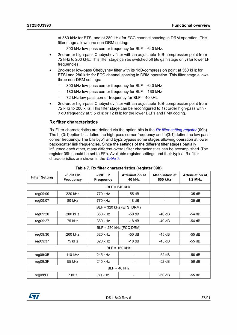
DS11840 Rev 6 37/91
ST25RU3993 Functional overview
46
at 360 kHz for ETSI and at 280 kHz for FCC channel spacing in DRM operation. This filter stage allows one non-DRM setting:
– 800 kHz low-pass corner frequency for BLF = 640 kHz.
• 2nd-order high-pass Chebyshev filter with an adjustable 1dB-compression point from 72 kHz to 200 kHz. This filter stage can be switched off (its gain stage only) for lower LF frequencies.
• 2nd-order low-pass Chebyshev filter with its 1dB-compression point at 360 kHz for ETSI and 280 kHz for FCC channel spacing in DRM operation. This filter stage allows three non-DRM settings:
– 800 kHz low-pass corner frequency for BLF = 640 kHz
– 180 kHz low-pass corner frequency for BLF = 160 kHz
– 72 kHz low-pass corner frequency for BLF = 40 kHz
• 2nd-order high-pass Chebyshev filter with an adjustable 1dB-compression point from 72 kHz to 200 kHz. This filter stage can be reconfigured to 1st order high-pass with -3 dB frequency at 5.5 kHz or 12 kHz for the lower BLFs and FM0 coding.
Rx filter characteristics
Rx Filter characteristics are defined via the option bits in the Rx filter setting register (09h). The hp[3:1]option bits define the high-pass corner frequency and lp[3:1] define the low pass corner frequency. The bits byp1 and byp2 bypass some stages allowing operation at lower back-scatter link frequencies. Since the settings of the different filter stages partially influence each other, many different overall filter characteristics can be accomplished. The register 09h should be set to FFh. Available register settings and their typical Rx filter characteristics are shown in the Table 7.
Table 7. Rx filter characteristics (register 09h)
Filter Setting-3 dB HP
Frequency-3dB LP
FrequencyAttenuation at
40 kHzAttenuation at
600 kHzAttenuation at
1.2 MHz
BLF = 640 kHz
reg09:00 220 kHz 770 kHz -55 dB - -35 dB
reg09:07 80 kHz 770 kHz -18 dB - -35 dB
BLF = 320 kHz (ETSI DRM)
reg09:20 200 kHz 380 kHz -50 dB -40 dB -54 dB
reg09:27 75 kHz 380 kHz -18 dB -40 dB -54 dB
BLF = 250 kHz (FCC DRM)
reg09:30 200 kHz 320 kHz -50 dB -45 dB -55 dB
reg09:37 75 kHz 320 kHz -18 dB -45 dB -55 dB
BLF = 160 kHz
reg09:3B 110 kHz 245 kHz - -52 dB -56 dB
reg09:3F 55 kHz 245 kHz - -52 dB -56 dB
BLF = 40 kHz
reg09:FF 7 kHz 80 kHz - -60 dB -55 dB
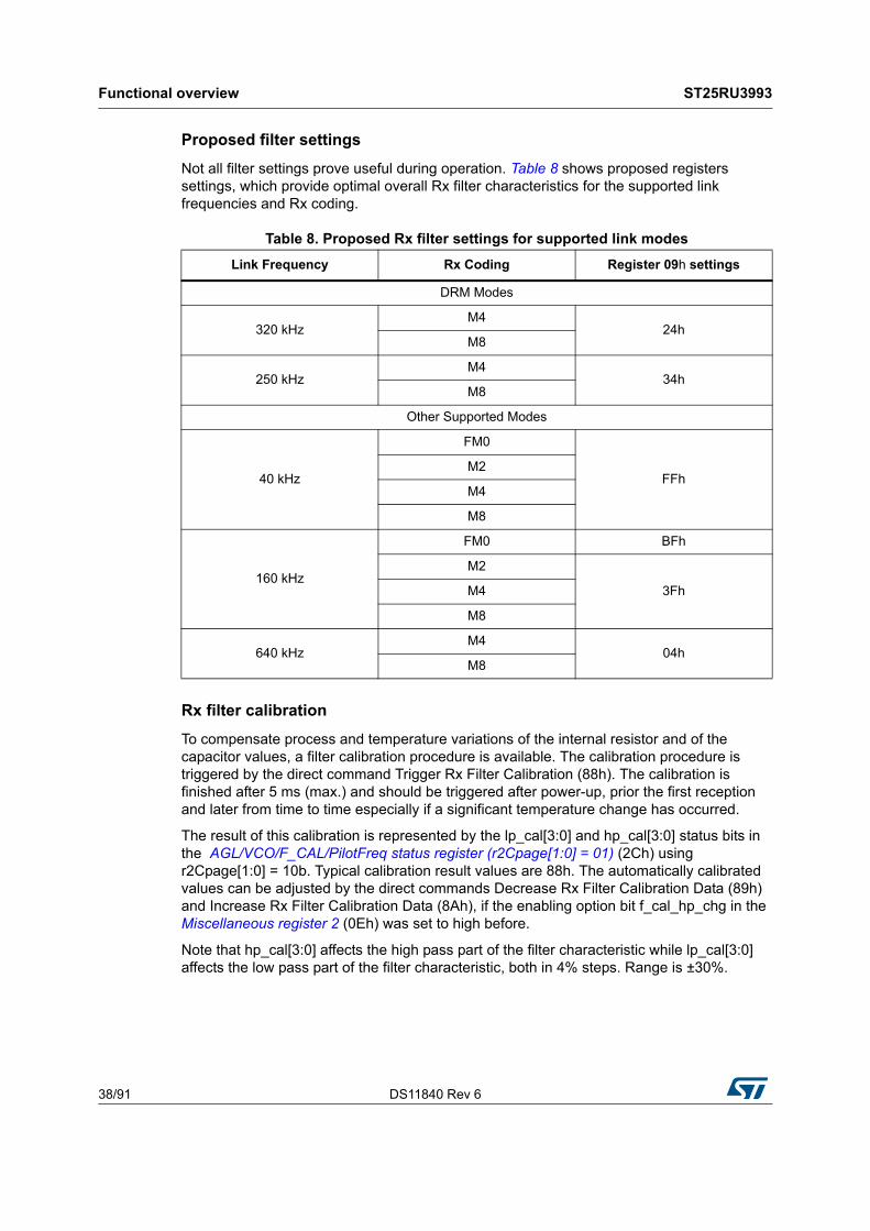
Functional overview ST25RU3993
38/91 DS11840 Rev 6
Proposed filter settings
Not all filter settings prove useful during operation. Table 8 shows proposed registers settings, which provide optimal overall Rx filter characteristics for the supported link frequencies and Rx coding.
Rx filter calibration
To compensate process and temperature variations of the internal resistor and of the capacitor values, a filter calibration procedure is available. The calibration procedure is triggered by the direct command Trigger Rx Filter Calibration (88h). The calibration is finished after 5 ms (max.) and should be triggered after power-up, prior the first reception and later from time to time especially if a significant temperature change has occurred.
The result of this calibration is represented by the lp_cal[3:0] and hp_cal[3:0] status bits in the AGL/VCO/F_CAL/PilotFreq status register (r2Cpage[1:0] = 01) (2Ch) using r2Cpage[1:0] = 10b. Typical calibration result values are 88h. The automatically calibrated values can be adjusted by the direct commands Decrease Rx Filter Calibration Data (89h) and Increase Rx Filter Calibration Data (8Ah), if the enabling option bit f_cal_hp_chg in the Miscellaneous register 2 (0Eh) was set to high before.
Note that hp_cal[3:0] affects the high pass part of the filter characteristic while lp_cal[3:0] affects the low pass part of the filter characteristic, both in 4% steps. Range is ±30%.
Table 8. Proposed Rx filter settings for supported link modes
Link Frequency Rx Coding Register 09h settings
DRM Modes
320 kHzM4
24hM8
250 kHzM4
34hM8
Other Supported Modes
40 kHz
FM0
FFhM2
M4
M8
160 kHz
FM0 BFh
M2
3FhM4
M8
640 kHzM4
04hM8
DS11840 Rev 6 39/91
ST25RU3993 Functional overview
46
Rx gain and digitizer hysteresis
The Rx gain in the receiving chain and digitizer hysteresis can be adjusted to optimize the signal to noise and interference ratio. There are three ways for adjustment:
• Manual
• AGC
• AGL
Manual Adjustment
This adjustment method is done by setting option bits in the Rx mixer and gain register (0Ah). The bits gain[2:0] increase the digitizer hysteresis by 3 dB per step (7 steps) and the bits gain[5:4] change the baseband amplifier gain by 3 dB per step (3 steps). The sign of the change (increase or decrease) is defined by the option bit gain_sign.
AGC
The built-in AGC comprises a system acting during the first periods of the incoming preamble. It partly changes the digitizer hysteresis (steps 1 - 4) and partly the baseband gain (steps 5 - 7). The hysteresis and baseband gain are changed equally for both channels maintaining the ratio between the I and Q channel so that the stronger signal is correctly digitized. The AGC can be enabled by setting the option bit agc_on in the Device status control register (00h) to high. The status of the AGC can be seen by the agc[2:0] status bits in the AGC and internal status display register (2Ah). The register value represents the number of 3 dB steps.
AGL
This adjustment is another possibility to decrease the sensitivity in case of bad reception conditions due to environmental noise and interferences. The AGL can be triggered by the direct command AGL On (A6h), during rf_ok = 1 after the direct command Enable Rx (97h) has been sent and during a period when there is no actual transponder response pending. This means that the RF ramp-up must be finished and the receiver is ready to receive the interference signals. This automatic feature increases the digitizer hysteresis for each channel independently to a level just above the noise and interference level. The maximum time required for the AGL action is 1 ms. The AGL result status for each channel can be seen by reading the agl[5:0] status bits in the AGL/VCO/F_CAL/PilotFreq status display register (r2Cpage[1:0] = 00) (2Ch) using r2Cpage[1:0] = 00b. The register values represent the number of 3 dB steps. There are four active steps available, while steps 5 - 7 are inactive (0 dB). The AGL is disabled by AGL Off (A7h) direct command. The result is stored and remains valid until the direct command AGL Off (A7h) was sent.
The difference between AGC and AGL is that AGC runs each time at the beginning of the data packet reception, while AGL only runs when the direct command AGL On (A6h) is sent.
Both AGC and AGL operate on the gain[2:0] bits in the Rx mixer and gain register (0Ah) and should be used exclusively. The manual setting has lower priority. In general, the system gain should be set to a level, that in good (normal) conditions only a small number of transitions occur on the digitizer output when no tag is transmitting. In such a case, also no AGL change would be seen.
2.9.5 IQ selection
The two receiving signals are digitized and evaluated. The decision circuit selects the in-phase signal or quadrature signal channel, whichever presents the better received signal,

Functional overview ST25RU3993
40/91 DS11840 Rev 6
for further processing. The chosen signal channel can be seen by reading the in_select status bit in the AGL/VCO/F_CAL/PilotFreq status display register (r2Cpage[1:0] = 00) (2Ah). This bit is valid from the end of the preamble until the start of the next transmission. For FM0 Rx encoding the selection is based on the evaluation of the digital representation of the received sub-carriers at the beginning of the data packet. For Miller Rx encoding the selection is supported by the logarithmic RSSI measurement. RSSI will be taken into account if at least one RSSI reading (I or Q) is higher than defined by the IQsel_Th[3:0] option bits in the Interrogator collision detection and IQ selection settings register (1Dh). Further improvements can be achieved by taking noise RSSI into account. To enable this mode (an active RF field and all mixer and gain settings as used for the subsequent reception are required) send the direct commands Enable Rx (97h) and Store RSSI (A8h). As a result only the difference between actual pilot RSSI and the stored noise RSSI will contribute to the IQ decision.
2.9.6 Bit decoder
The bit decoder converts the sub-carrier coded signals to a bit stream data according to the protocol defined by the option bits RX_cod[2:0 and RX_LF[3:0] in the Rx options register (03h). The system extracts the data clock and serial data bits, and removes the preamble. The decoder logic is designed for maximum error tolerance to enable successful decoding of partly corrupted sub-carrier signals due to noise or interference. In the EPC Class1 Gen2 protocol, the decoder supports long Rx preamble (TRext = 1) for FM0, and all Miller encoded signals. Short Rx preamble (TRext = 0) is supported for Miller4 and Miller8 encoded signals.
2.9.7 Data framer
In the data framer, the serial bit stream is formatted into bytes. The CRC bytes are checked and removed leaving pure baseband data, which is sent to the 24-byte FIFO register from where it can be read out by the MCU. The receiver also supports transfer of incomplete bytes.
2.10 Data reception modes
The device can operate in the normal mode or in direct mode.
2.10.1 Rx normal mode
In the normal mode the received data is stored in FIFO.
Reception start
The reception is triggered automatically at the end of the data transmission.
The second option to start the reception is done manually by sending the direct command Enable Rx (97h). For correct operation, the dir_mode bit in the Protocol selection register (01h) should be set to 0.
The third possibility to start reception is using one of the AutoACK modes, which automatically triggers the reception to acquire PC+EPC and Handle.
DS11840 Rev 6 41/91
ST25RU3993 Functional overview
46
Rx wait timer
The Rx wait timer defines a wait time between the end of data transmission and start of data reception. During this period, the decoder is not active. This prevents any incorrect detection that could occur due to transients caused by transmit operation, by noise or interference. The Rx wait time setting is done by the RXw[7:0] option bits in the Rx wait time register (08h). The step size for the Rx wait time is 6.4 µs.
Rx no response timer
The Rx no response timer starts with the reception slot of the anti-collision algorithm until a tag response arrives. In case no tag response is received during the defined time, the reception terminates and an IRQ is triggered with the Irq_noresp bit set. In case the e_irq_noresp option bit in the Enable interrupt register 1 (35h) is set, the reception is not terminated by the Rx No Response Timer. Therefore the reception needs to be terminated manually by sending the direct command Block Rx (96h). This mode is designed for commands where the response time can be long or not defined. The Rx no response timer is controlled by the Rx no response time register (07h). This time is defined in 25.6 µs steps. In case the timer is set to FFh the Rx no response time is fixed to 26.2 ms.
Decoder operation
During data reception the Rx_status bit in the FIFO status register (39h) is set high and when the data transmission is finished, the reader device issues an IRQ request with the Irq_RX bit set. In the Rx FIFO buffer 24 bytes can be stored. In case the number of received data bytes is higher than 18, an IRQ request with the Irq_fifo bit set high (register 37h) signals to the MCU that data should be removed from the FIFO. If an error in the data format or in the CRC is detected, the MCU is alerted by an IRQ request with the Irq_err bit set to high. Information about the cause for the error can be read from the Interrupt register 2 (38h). In case of a reception error, the system still receives the expected number of bits, to maintain a similar time flow for the reader and the tags.
Rx length register
Typically the expected reception length should be defined before the reception start. If this is not the case the reception length is updated during the reception when the actual length becomes available. When the reception is triggered at the end of normal data transmission (direct commands 90h, 91h, 92h), the reception length needs to be defined by the RXl[11:0] option bits in the Rx length register 1 and Rx length register 2 (3Ah, 3Bh).
For the direct Query commands (98h, 99h, 9Ah, 9Bh, 9Ch), the Rx length is predefined to 16 bits for the awaited RN16. For the direct command ReqRN (9Fh) the Rx length is internally set to 32 bits in order to receive handle and CRC. Only during the reception of the PC + EPC the reception length is not known in advance. To cover this case, the internal protocol logic checks the first received byte and adjusts the Rx length according to the value found in the first PC byte. In case reception is triggered manually by the direct command Enable Rx (97h), the Rx length needs to be set by the RXl[11:0] option bits in the Rx length register 1 and Rx length register 2 (3Ah, 3Bh). If one of the AutoACK procedures is used, the Rx length is automatically set for all tag responses received during the automatic inventory command sequence.
If the automatically set Rx length does not fit the actual tag data length, possibly due to future protocol extensions or custom tag functionality, the MCU can change the expected Rx length during reception. In case of automatically set PC+EPC length, the length change is possible after the second received byte. The MCU can request an additional interrupt after

Functional overview ST25RU3993
42/91 DS11840 Rev 6
receiving two bytes (PC part of the PC + EPC field). The MCU can read out the two bytes that define the length of the on-going reception and update the Rx length register. The IRQ request after the 2nd byte is enabled by the fifo_dir_irq2 option bit in the Rx length register 1 (3Ah). The side effect of this mode is that CRC bytes become available in the FIFO as well. The actual reception of the second byte is signaled by the Irq_2nd_byte IRQ bit set to high in the Interrupt register 1 (37h). If the actual Rx length is only available later, it is possible to extend the 2nd byte interrupt functionality to trigger additional IRQ requests after the 4th, 6th … received byte by setting the rep_irq2 option bit in the Rx length register 1 (3Ah). When the interrupt after the targeted number of received bytes is received, clearing the rep_irq2 option bit prevents extra interrupts for the rest of the reception.
For some Gen2 commands the tag can reply with a normal response or an error code. The two types of responses are different in length. For further MCU relief the auto_errcode_RXl option bit was prepared. When this option bit is set, the protocol logic checks the received header bit and adjusts its expected reception length to 41 bits (Gen2 error response length) if it detects an error code reception.
RN16 register
In the EPC Class1 Gen2 protocol, the timing between a tag response and the subsequent reader command in the inventory round is relatively short. To help the MCU from reading the RN16 (or handle) from the FIFO and then writing it back to the FIFO, a special register for storing the last received RN16 is built into the device. The RN16 is stored after the last successful reception upon one of the direct Query commands. The last stored RN16 is automatically used in the ACK command.
AutoACK modes
The AutoACK mode automatically performs the inventory command sequence for one transponder. The aim is relieve the MCU of time critical tasks by minimizing the number of interactions between the MCU and the reader device. The AutoACK mode is enabled by setting the AutoACK[1:0] option bits in the Protocol selection register (01h). Following modes are available:
• AutoACK[1:0] = 00b: Query only
• AutoACK[1:0] = 01b: Each query command is followed by an ACK
• AutoACK[1:0] = 10b: Each query command is followed by an ACK and ReqRN
The automatic inventory command sequence is triggered by the direct Query commands (98h, 99h, 9Ah, 9Bh, 9Ch). After successful RN16 reception, it automatically prepares and triggers the acknowledge command ACK and subsequent receptions. After successful reception of the PC+EPC, it automatically prepares and triggers the request for a handle (ReqRN) It also prepares the appropriate Rx length settings and provides the received data (PC+EPC, Handle) in the FIFO. The MCU reads out the baseband data and triggers next Query command to continue the inventory round or another tag command that can be used in tag open state.

DS11840 Rev 6 43/91
ST25RU3993 Functional overview
46
The number of interrupts that need to be serviced by the host system (MCU) is minimized:
• Irq_noresp is signaled if nothing is received.
• Irq_fifo is signaled if EPC is longer than 18 bytes. It informs that data should be read out from the FIFO.
• Irq_RX is signaled at the end of the EPC and Handle reception. This also tells that one AutoACK step is finished. Available data should be read out from the FIFO buffer if of no error.
• Irq_AutoACK is signaled at the end of the AutoACK procedure, meaning that a RN16 was received and that at least the ACK command was issued during the sequence.
• Irq_err is signaled if an error occurred during the procedure.
To successfully control the inventory round, the host system needs to distinguish between empty anti-collision slots and collided slots:
• Irq_noresp without Irq_AutoACK means that there was no response to a Query command. This presents a real empty slot in the inventory procedure.
• Irq_noresp with Irq_AutoACK or Irq_err with Irq_AutoACK means that RN16 was received, and that the empty slot or reception error happened later in the procedure. Probably some unidentified transponders are present in the field. But it could also mean that for particular settings and conditions, the filtered received noise level is above the digitizing hysteresis threshold and that the system recognizes it as tag signal.
The AutoACK function uses the Rx no response time register (07h) and Rx wait time register (08h) as they are used in other normal mode reception cases. An additional timer is used to define the T2 time according to the EPC Class1 Gen2 protocol. This time is defined in the AutoACK wait time register (06h). The timer is started at the end of the reception period and defines when the subsequent data transmission is triggered.
Normal mode with test outputs
Following possibilities in the Measurement control register (10h) are available to observe operation in normal mode and during board debugging:
• Digitized sub-carrier signals of both receiving channels (I and Q) are enabled by setting the option bits Tcomb[1:0] = 01b. Outputs are OAD and OAD2.
• The Tx modulation output and the selected digitized sub-carrier signal channel are enabled by setting the option bits Tcomb[1:0] = 10b. Outputs are OAD (TX) and OAD2 (Rx).
• Analog sub-carrier signals of both receiving channels (I and Q) are enabled by setting the option bits e_anaout[1:0] = 01b. Outputs are OAD and OAD2. Analog output has lower priority than the digital output.
2.10.2 Rx direct mode
Reception in the direct mode is triggered by setting the pin SCLK (Enable Rx input) to high. When receiving data from a tag in direct mode, there are three possibilities depending on option bits setting:
• Internally decoded bit stream and bit clock according to the protocol is enabled by dir_mode = 0 and defined by the option bits prot[2:0] in the Protocol selection register (01h), RX_cod[2:0] and RX_LF[3:0] option bits in the Rx options register (03h). The

Functional overview ST25RU3993
44/91 DS11840 Rev 6
outputs are the pins MISO and IRQ.
• Digitized sub-carrier signals of both receiving channels (I and Q) are enabled by setting the option bit dir_mode in the Protocol selection register (01h) to high. The outputs are the pins MISO and IRQ.
• Analog sub-carrier signals of both receiving channels (I and Q) are enabled by setting the option bits e_anaout[1:0] in the Measurement control register (10h) to 01b. The outputs are the pins OAD and OAD2.
For details on how to enter the direct mode and the re-assignments of the I/O pins in this mode refer to the Section 2.8.2: TX direct mode.
2.10.3 Modes supporting tuning of antenna or directivity device
In order to achieve low reflected Tx power the user has to actively tune the antenna or the direct device. To enable correct tuning the amplitude and the phase information of the incoming reflected power is available through the output DC levels of the two mixers. The analog representation of the two mixer DC level outputs is available on the OAD and OAD2 outputs by setting e_anaout[1:0] = 10b in the Measurement control register (10h). If the user does the tuning during reception, the Enable_RX signal is required to know when the receiver is enabled. This information is available on ADC pin if Tcomb[1:0] = 11b in the Measurement control register (10h). Another approach to acquire the tuning data is to read the digital representation of the reflected power level as described in the A/D Converter section.
2.10.4 Logarithmic RSSI
The receiver section comprises two logarithmic RSSI (Received Signal Strength Indicator) blocks. They are connected to the outputs of both signal channels (I and Q). The value of each RSSI reading is stored during the data reception at the second received byte in the RSSI display register (2Bh) using r2Bpage[3:0] = 0110b. The RSSI result is valid until the start of the next transmission.
2.11 A/D converter
An 8-bit on board A/D converter supports an external power detector and can be connected to the internal diagnostic circuitry. The input range is ±1V, centered at the AGD voltage (1.6 V). The 7 LSBs give information about the absolute output level, while the MSB acts as a sign bit (while high indicates positive values, and low means negative values). The source for A/D conversion is selected through the msel[3:0] option bits in the Measurement control register(10h). The conversion is triggered by the direct command Trigger AD conversion (87h) and the result is available through the ADC readout/regulator setting display register (r2Dpage[1:0] = 00) (2Dh) using r2Dpage[1:0] = 00b (Status readout page setting register). The A/D conversion is finished after 20 µs and an IRQ request is sent with the Irq_cmd option bit set (Interrupt register 2).
2.11.1 External RF power detector
An external RF power detector can be placed after the PA or at the input coupled port of a directional coupler, making it possible to measure actual RF output power. The resulting analog voltage from the power detector can be connected to the ADC pin of the reader device. The digital representation of this voltage level can be acquired with the on board A/D converter using msel[3:0] = 0011b (Measurement control register).

DS11840 Rev 6 45/91
ST25RU3993 Functional overview
46
2.11.2 Reflected RF power indicator
The receiver comprises an input RF level indicator, used for diagnostic purposes of the circuitry or for detecting environmental difficulties around the antenna. Reflections from poor antennas (S11), the reflective antenna’s environment and directional device leakage increase the carrier level (self-jammer level) at the mixer input. Since a higher carrier level causes an increase of demodulated noise, it is mandatory to keep the unwanted carrier level at the mixer input at a minimum. The reflected carrier that is seen on the two mixers inputs is down-converted to zero frequency. The two DC levels on the mixers outputs are proportional to the input RF level and can be used as a measure for the RF input level. The mixer DC levels are also dependent on the carrier input phase. The two mixer DC output levels can be connected to the on-board A/D converter by setting the option bits msel[3:0] = 0001b and 0010b. The id2x and id1x5 option bits adapt the gain of the reflected RF power level indicator.
2.11.3 Supply voltage measurement
The A/D converter can be also used to measure the supply voltages VEXT, VEXT_PA, VDD_B, and VDD_PA. Depending on the conversion results the MCU can decide on the voltage regulator setting strategy. The selected voltage is connected to A/D converter input (VINPUT) by setting the option bit to msel[3:0]:
• VEXT: 0111b
• VDD_B: 1000 b
• VEXT_PA: 1001 b
• VDD_PA: 1010 b
The conversion is started by the direct command Trigger AD conversion (87h) and the result is available in the ADC readout/regulator setting display register (r2Dpage[1:0] = 01) (2Dh) using r2Dpage[1:0] = 00b (Status readout page setting register).
The conversion result is given by the equation:
where the ADC register value is the value in register 2Dh and Vinput is the analog voltage present at the A/D converter input in volts.
2.11.4 Linear RSSI with sub-carrier phase bit
The demodulated peak-to-peak voltages of both signal channels (I and Q) are connected to a double sample and hold circuit and are sampled at the end of the tag-preamble (pilot tone). They can be A/D converted during or after the reception. The MCU can convert and read out the two voltages using the internal linear A/D converter by setting the option bits msel[3:0] = 1011b and msel[3:0] = 1100b (Measurement control register) and triggering the conversion by the direct command Trigger AD conversion (87h). The results are available in the ADC readout/regulator setting display register (r2Dpage[1:0] = 01) (2Dh) using r2Dpage[1:0] = 00b (Status readout page setting register). For the linear RSSI, the sampled voltages are shifted to use the whole ADC range. The minimum sample value gives -127 as
ADC register valueVinput 1.6–( ) 0.8⋅ 1.6–
0.0079-------------------------------------------------------------------=

Functional overview ST25RU3993
46/91 DS11840 Rev 6
ADC result, and the maximum sample value gives +127 as ADC result. The status bit subc_phase in the AGC and internal status display register (2Ah) shows whether the two sampled peak-to-peak voltages (I and Q) were in phase or in anti-phase at the moment of sampling. The phase bit is valid from the end of pilot tone till the end of reception and should be read out before the end of reception. Using the linear (absolute) I and Q RSSI values and the phase bit information the systems allows detecting the RSSI phase information within.
2.11.5 Internal signal level detectors
An internal signal level detector is placed at the output of the internal VCO and therefore enables the measurement of the internal RF carrier level. The selected source is connected to the A/D converter input through the option bits msel[3:0] = 0100b. For a description of the conversion procedure refer to the A/D converter description. The internal signal level detector is meant for diagnostic purposes only and should not be used for measurement of the output power.
2.12 Interrogator anti-collision support
To enable the ISO 29143 functionality, a RSSI based interrogator anti-collision support is arranged. The feature is enabled by the direct command Interrogator Anti-collision Support Enable (AAh). According to the ISO 29143 proposal, the system monitors the RSSI envelope of the received sub-carrier signals and informs the MCU in case at least in a part of the received data packet the RSSI level has exceeded the predefined threshold. It also stores RSSI and timing data of the data packet at relevant points.
Following RSSI values are stored:
• RSSI at pilot tone
• RSSI at data
• Maximum RSSI value in the telegram
Following timing data are stored:
• First time at which the predefined threshold was exceed
• Threshold exceedance duration
• Time of first protocol violation
Time is related to the received bits.
The predefined collision detection threshold is in the ICD_Th[3:0] bits in the Interrogator collision detection and IQ selection settings register (1Dh). To enable the functionality the direct command Interrogator Anti-collision Support Enable (AAh) needs to be sent. To disable it the Interrogator Anti-collision Support Disable (ABh) direct command should be used. To clear the peak RSSI value and timing data again use the Interrogator Anti-collision Support Disable (ABh) direct command.

DS11840 Rev 6 47/91
ST25RU3993 Register description
78
3 Register description
The 6-bit long register addresses are shown in the hexadecimal notation. There are two types of registers implemented in the reader device:
• Read/Write registers
• Read-only display registers.
They can be accessed via the serial interface.
Table 9. Registers map
Address(hex)
Main function Content Type
00Main control
Device status control register RW
01 Protocol selection register RW
02
Configuration
Tx options register RW
03 Rx options register RW
04 TRcal high register RW
05 TRcal low register RW
06 AutoACK wait time register RW
07 Rx no response time register RW
08 Rx wait time register RW
09 Rx filter setting register RW
0A Rx mixer and gain register RW
0B Regulator and PA bias register RW
0C RF output and LO control register RW
0D Miscellaneous register 1 RW
0E Miscellaneous register 2 RW
10 Measurement control register RW
11 VCO control register RW
12 CP control register RW
13 Modulator control register 1 RW
14 Modulator control register 2 RW
15 Modulator control register 3 RW
16 Modulator control register 4 RW
17 PLL main register 1 RW
18 PLL main register 2 RW
19 PLL main register 3 RW
1A PLL auxiliary register 1 RW
1B PLL auxiliary register 2 RW

Register description ST25RU3993
48/91 DS11840 Rev 6
In the register description tables the bit names along with their default value after device power-up (EN=L). A short function description and comment are given.
3.1 Main control registers
In the Register Description tables the bit names along with their default value after device power-up (EN = L). A short function description and comment are given.
1C
Configuration
PLL auxiliary register 3 RW
1DInterrogator collision detection and IQ selection settings register
RW
22 Emitter-coupled mixer options register RW
29
Status
Status readout page setting register RW
2A AGC and internal status display register R
2B RSSI display register R
2C
AGL/VCO/F_CAL/PilotFreq status display register (r2Cpage[1:0] = 00)
R
AGL/VCO/F_CAL/PilotFreq status register (r2Cpage[1:0] = 01)
R
2DADC readout/regulator setting display register (r2Dpage[1:0] = 00)
R
2E Command status display register R
33 Version register R
35
Interrupt
Enable interrupt register 1 RW
36 Enable interrupt register 2 RW
37 Interrupt register 1 R
38 Interrupt register 2 R
39
Communication
FIFO status register R
3A Rx length register 1 RW
3B Rx length register 2 RW
3C Tx setting register RW
3D Tx length register 1 RW
3E Tx length register 2 RW
3F FIFO I/O registerTx: WRx: R
Table 9. Registers map (continued)
Address(hex)
Main function Content Type

DS11840 Rev 6 49/91
ST25RU3993 Register description
78
3.1.1 Device status control register
Address: 00h
Type: RW
3.1.2 Protocol selection register
Address: 01h
Type: RW
Table 10. Device status control register
Bit Name Default Function Comments
7 stby 0 Stand-by mode 0: Normal mode
1: Standby mode
6 RFU 0 Not used RFU, do not set
5 RFU 0 Not used RFU, do not set
4 RFU 0 Not used RFU, do not set
3 RFU 0 Not used RFU, do not set
2 agc_on 0 AGC enable0: AGC OFF
1: AGC ON
1 rec_on 0 Receiver enable0: The receiver is disabled
1: The receiver is enabled
0 rf_on 0Transmitter and receiver enable
0: Tx RF field and receiver are disabled
1: Tx RF field and receiver are enabled
Table 11. Protocol selection register
Bit Name Default Function Comments
7 RX_crc_n 0Receiving without
CRC0: Rx with CRC
1: Rx without CRC
6 dir_mode 0 Decoder mode type
0: Normal operation
1: Disables any decoding and signal sensing automatics in the receiver. It is advised to set this bit high when continuous analog measurements are performed.
5 AutoACK[1] 0
AutoAck mode
00: No Auto ACK
01: AutoACK
10: AutoACK+ReqRN
11: RFU, do not set4 AutoACK[0] 0
3 RFU 0 Not used RFU, do not set
2 prot[2] 0
Protocol selection
000: EPC Class1 Gen2/ISO18000-6C
001: ISO18000-6 Type A/B direct mode decoder enable
Others: RFU, do not set
1 prot[1] 0
0 prot[0] 0

Register description ST25RU3993
50/91 DS11840 Rev 6
3.2 Configuration registers
3.2.1 Tx options register
Address: 02h
Type: RW
3.2.2 Rx options register
Address: 03h
Type: RW
Table 12. Tx options register
Bit Name Default Function Comments
7 RFU 0 Not used RFU, do not set
6 RFU 0 Not used RFU, do not set
5 TXOne[1] 1
Tx one length control
00: 1.50 * Tari
01: 1.66 * Tari
10: 1.83 * Tari
11: 2.00 * Tari4 TXOne[0] 1
3 RFU 0 Not used RFU, do not set
2 Tari[2] 0
Tari definition
000: Tari = 6.25 µs
001: Tari = 12.5 µs
010: Tari = 25 µs
Others: RFU, do not set
1 Tari[1] 1
0 Tari[0] 0
Table 13. Rx options register
Bit Name Default Function Comments
7 RX_LF[3] 1
Link frequency
0000: 40 kHz
0110: 160 kHz
1001: 250 kHz
1100: 320 kHz
1111: 640 kHz
Other: RFU, do not set
6 RX_LF[2] 1
5 RX_LF[1] 0
4 RX_LF[0] 0
3 TRext 1 Rx preamble length
0: Short preamble
1: Long preamble
Short preamble is supported for Miller 4 and Miller 8 coding.
2 RX_cod[2] 0
Rx coding
000: FM0
001: M2
010: M4
011: M8
Other: RFU, do not set
1 RX_cod[1] 1
0 RX_cod[0] 0

DS11840 Rev 6 51/91
ST25RU3993 Register description
78
3.2.3 TRcal high register
Address: 04h
Type: RW
3.2.4 TRcal low register
Address: 05h
Type: RW
Table 14. TRcal high register
Bit Name Default Function Comments
7 low_vsp_lo 0 low_vsp_lo1: Adaptation to low supply for the LO phase shifter
6 id2x 0 id2xAdapt gain 2x of the reflected RF power level
(mixer DC level) indicator
5 id1x5 0 id1x5Adapt gain 1.5x of the reflected RF power level
(mixer DC level) indicator
4 RFU Not used RFU, do not set
3 TRcal[11] 0
TRcal[11:0] bits define TRcal time
Description in register 05h2 TRcal[10] 0
1 TRcal[9] 1
0 TRcal[8] 0
Table 15. TRcal low register
Bit Name Default Function Comments
7 TRcal[7] 1
TRcal[11:0] bits define TRcal time
Range: 0.1 µs - 409 µs
Steps: 4096
Step size: 0.1 µs Worst case relative resolution in Gen 2 range: %
Gen2 defines a range from 17.2 µs to 225 µs
6 TRcal[6] 0
5 TRcal[5] 0
4 TRcal[4] 1
3 TRcal[3] 1
2 TRcal[2] 0
1 TRcal[1] 1
0 TRcal[0] 1
0.1μs17.2μs------------------ 0.6≈
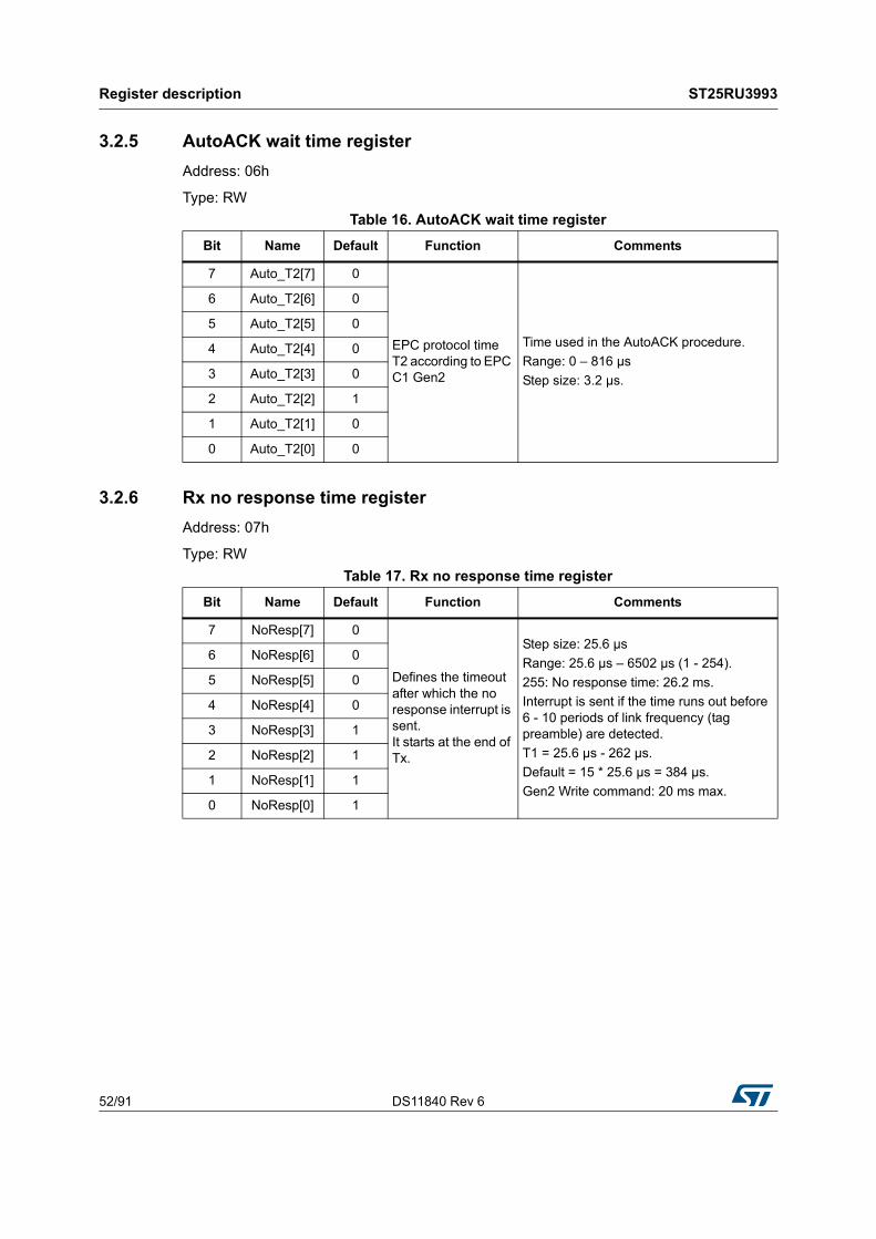
Register description ST25RU3993
52/91 DS11840 Rev 6
3.2.5 AutoACK wait time register
Address: 06h
Type: RW
3.2.6 Rx no response time register
Address: 07h
Type: RW
Table 16. AutoACK wait time register
Bit Name Default Function Comments
7 Auto_T2[7] 0
EPC protocol time T2 according to EPC C1 Gen2
Time used in the AutoACK procedure.
Range: 0 – 816 µs
Step size: 3.2 µs.
6 Auto_T2[6] 0
5 Auto_T2[5] 0
4 Auto_T2[4] 0
3 Auto_T2[3] 0
2 Auto_T2[2] 1
1 Auto_T2[1] 0
0 Auto_T2[0] 0
Table 17. Rx no response time register
Bit Name Default Function Comments
7 NoResp[7] 0
Defines the timeout after which the no response interrupt is sent. It starts at the end of Tx.
Step size: 25.6 µs
Range: 25.6 µs – 6502 µs (1 - 254).
255: No response time: 26.2 ms.
Interrupt is sent if the time runs out before 6 - 10 periods of link frequency (tag preamble) are detected.
T1 = 25.6 µs - 262 µs.
Default = 15 * 25.6 µs = 384 µs.
Gen2 Write command: 20 ms max.
6 NoResp[6] 0
5 NoResp[5] 0
4 NoResp[4] 0
3 NoResp[3] 1
2 NoResp[2] 1
1 NoResp[1] 1
0 NoResp[0] 1

DS11840 Rev 6 53/91
ST25RU3993 Register description
78
3.2.7 Rx wait time register
Address: 08h
Type: RW
3.2.8 Rx filter setting register
Address: 09h
Type: RW
Table 18. Rx wait time register
Bit Name Default Function Comments
7 RXw[7] 0
Rx wait time.
Defines the time during which the Rx input is ignored.
It starts from the end of Tx.
Step size: 6.4 µs
Range: 6.4 µs – 1632 µs (1 - 255),
00h: The receiver is enabled immediately after Tx
Gen2: T1min = 11.28 µs - 262 µs.
ISO1800-6A: 150 µs - 1150µs
ISO1800-6B: 85 µs - 460µs
Default = 7 * 6.4 µs = 44.8 µs.
6 RXw[6] 0
5 RXw[5] 0
4 RXw[4] 0
3 RXw[3] 0
2 RXw[2] 1
1 RXw[1] 1
0 RXw[0] 1
Table 19. Rx filter setting register
Bit Name Default Function Comments
7 byp2 0 bypass 2
Set to FFh: 40 kHz link frequency
6 byp1 0 bypass 1
5 lp[3] 1
Low pass setting4 lp[2] 0
3 lp[1] 0
2 hp[3] 1
High pass setting1 hp[2] 0
0 hp[1] 0

Register description ST25RU3993
54/91 DS11840 Rev 6
3.2.9 Rx mixer and gain register
Address: 0Ah
Type: RW
Table 20. Rx mixer and gain register
Bit Name Default Function Comments
7 gain[5] 0
Baseband gain change
Steps: 4
Step Size:3 dB
00: 0 dB
11: 9 dB
Increase/decrease defined by gain_sign option bit
6 gain[4] 0
5 gain_sign 0Sign bit for BB gain settings (gain[5:4])
0: Decrease baseband gain
1: Increase baseband gain
4 gain[2] 0
Digitizer hysteresis increase
Steps: 5
Step Size: 3 dB
000: 0 dB
100: 12 dB
Other: RFU, do not set
3 gain[1] 0
2 gain[0] 0
1 mix_ir[1] 0
Mixer gain and input range selection
Differential Rx mixer:
– 00: Nominal gain
– 01: 8 dB attenuation
– 10: 10 dB gain increase
Single ended Rx mixer:
– 00: 6 dB mixer gain decrease
– 01: Nominal gain
– 11: 6 dB mixer gain increase
0 mix_ir[0] 1
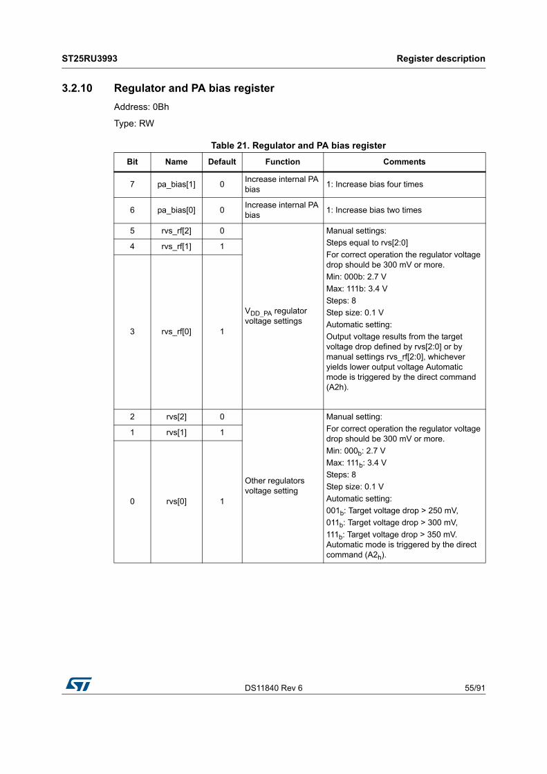
DS11840 Rev 6 55/91
ST25RU3993 Register description
78
3.2.10 Regulator and PA bias register
Address: 0Bh
Type: RW
Table 21. Regulator and PA bias register
Bit Name Default Function Comments
7 pa_bias[1] 0Increase internal PA bias
1: Increase bias four times
6 pa_bias[0] 0Increase internal PA bias
1: Increase bias two times
5 rvs_rf[2] 0
VDD_PA regulator voltage settings
Manual settings:
Steps equal to rvs[2:0]
For correct operation the regulator voltage drop should be 300 mV or more.
Min: 000b: 2.7 V
Max: 111b: 3.4 V
Steps: 8
Step size: 0.1 V
Automatic setting:
Output voltage results from the target voltage drop defined by rvs[2:0] or by manual settings rvs_rf[2:0], whichever yields lower output voltage Automatic mode is triggered by the direct command (A2h).
4 rvs_rf[1] 1
3 rvs_rf[0] 1
2 rvs[2] 0
Other regulators voltage setting
Manual setting:
For correct operation the regulator voltage drop should be 300 mV or more.
Min: 000b: 2.7 V
Max: 111b: 3.4 V
Steps: 8
Step size: 0.1 V
Automatic setting:
001b: Target voltage drop > 250 mV,
011b: Target voltage drop > 300 mV,
111b: Target voltage drop > 350 mV. Automatic mode is triggered by the direct command (A2h).
1 rvs[1] 1
0 rvs[0] 1

Register description ST25RU3993
56/91 DS11840 Rev 6
3.2.11 RF output and LO control register
Address: 0Ch
Type: RW
3.2.12 Miscellaneous register 1
Address: 0Dh
Type: RW
Table 22. RF output and LO control register
Bit Name Default Function Comments
7 eTX[7] 0LO (local oscillator) gain
0: Nominal
1: 6 dB gain in LO path
6 eTX[6] 0 LO source selection0: LO source is RFOPX, RFONX
1: LO source is pre-driver for the internal PA
5 eTX[5] 0Enable internal VDD_PA voltage regulator
VDD_PA regulator is automatically enabled if the internal PA is enabled via eTX[3:2]
4 RFU 0 Not used RFU, do not set
3 eTX[3] 0Main PA enable and bias current for main PA pre-driver
00: Disable
01: 7 mA
10: 14 mA
11: 22 mA2 eTX[2] 0
1 eTX[1] 1 Enable RF low-power output and bias current for RF output stage.
00: Disable
01: 7 mA
10: 14 mA (default)
11: 22 mA0 eTX[0] 0
Table 23. Miscellaneous register 1
Bit Name Default Function Comments
7 hs_output 1Strong, fast communication output drivers
Valid for MISO, IRQ, CLSYS
6 hs_oad 0Strong, fast test output drivers
Valid for OAD, OAD2, ADC
5 miso_pd2 0Pull down resistor: NCS = 0
1: Enable a pull down resistor on MISO, when NCS is low and MISO is not driven by the ST25RU3993
4 miso_pd1 0Pull down resistor: NCS = 1
1: Enable a pull down resistor on MISO when NCS is high
3 open_dr 0Open drain N-MOS outputs
Valid for MISO, IRQ, CLSYS
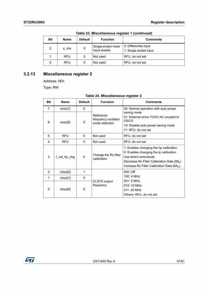
DS11840 Rev 6 57/91
ST25RU3993 Register description
78
3.2.13 Miscellaneous register 2
Address: 0Eh
Type: RW
2 s_mix 0Single-ended mixer input enable
0: Differential input
1: Single ended input
1 RFU 0 Not used RFU, do not set
0 RFU 0 Not used RFU, do not set
Table 23. Miscellaneous register 1 (continued)
Bit Name Default Function Comments
Table 24. Miscellaneous register 2
Bit Name Default Function Comments
7 xosc[1] 0
Reference frequency oscillator mode selection
00: Normal operation with auto power saving mode
01: External sinus TCXO AC coupled to OSCO
10: Disable auto power saving mode
11: RFU, do not set
6 xosc[0] 0
5 RFU 0 Not used RFU, do not set
4 RFU 0 Not used RFU, do not set
3 f_cal_hp_chg 0Change the Rx filter calibration
1: Enables changing the hp calibration
0: Enables changing the lp calibration
Use direct commands:
Decrease Rx Filter Calibration Data (89h)
Increase Rx Filter Calibration Data (8Ah).
2 clsys[2] 1
CLSYS output frequency
000: Off
100: 4 MHz
001: 5 MHz
010: 10 MHz
011: 20 MHz
Others: RFU, do not set
1 clsys[1] 0
0 clsys[0] 0

Register description ST25RU3993
58/91 DS11840 Rev 6
3.2.14 Measurement control register
Address: 10h
Type: RW
3.2.15 VCO control register
Address: 11h
Type: RW
Table 25. Measurement control register
Bit Name Default Function Comments
7 Tcomb[1] 0
Digital test output modes
00: Disable01: Digitized Rx sub-carriers outputs on OAD, OAD210: Tx modulation and selected Rx sub-carrier outputs on OAD, OAD211: Enable Rx output on ADC
6 Tcomb[0] 0
5 e_anaout[1] 0
Analog test output modes
00: Disable01: Analog sub-carrier out on OAD, OAD210: Analog mixer DC output on OAD, OAD211: RFU, do not set
4 e_anaout[0] 0
3 msel[3] 0
ADC measurement selection
0001: Mixer DC level I-channel0010: Mixer DC level Q-channel0011: ADC pin0100: Internal RF level0111: VEXT level
1000: VDD_B level
1001: VEXT_PA level
1010: VDD_PA level
1011: RSSI I level1100: RSSI Q level1111: RFOPX, RFONX power level0000: NC
2 msel[2] 0
1 msel[1] 0
0 msel[0] 0
Table 26. VCO control register
Bit Name Default Function Comments
7 mvco 0VCO measurement enable
Steps: 7Result in register 2Ch r2Cpage[1:0] = 01
6 eosc[2] 1
Internal oscillator bias current
8 steps,
Step size: 0.52 mA
000: Minimum bias current (~1.3 mA)
111: Maximum bias current (~5 mA)
5 eosc[1] 0
4 eosc[0] 0
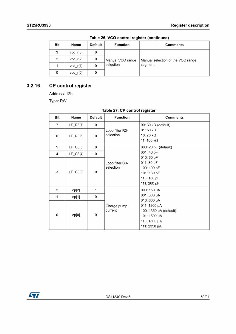
DS11840 Rev 6 59/91
ST25RU3993 Register description
78
3.2.16 CP control register
Address: 12h
Type: RW
3 vco_r[3] 0
Manual VCO range selection
Manual selection of the VCO range segment
2 vco_r[2] 0
1 vco_r[1] 0
0 vco_r[0] 0
Table 26. VCO control register (continued)
Bit Name Default Function Comments
Table 27. CP control register
Bit Name Default Function Comments
7 LF_R3[7] 0
Loop filter R3-selection
00: 30 kΩ (default)
01: 50 kΩ
10: 70 kΩ
11: 100 kΩ6 LF_R3[6] 0
5 LF_C3[5] 0
Loop filter C3-selection
000: 20 pF (default)
001: 40 pF
010: 60 pF
011: 80 pF
100: 100 pF
101: 130 pF
110: 160 pF
111: 200 pF
4 LF_C3[4] 0
3 LF_C3[3] 0
2 cp[2] 1
Charge pump current
000: 150 µA
001: 300 µA
010: 600 µA
011: 1200 µA
100: 1350 µA (default)
101: 1500 µA
110: 1800 µA
111: 2350 µA
1 cp[1] 0
0 cp[0] 0

Register description ST25RU3993
60/91 DS11840 Rev 6
3.2.17 Modulator control register 1
Address: 13h
Type: RW
3.2.18 Modulator control register 2
Address: 14h
Type: RW
Table 28. Modulator control register 1
Bit Name Default Function Comments
7 RFU 0 Not used RFU, do not set
6 main_mod 0Modulation connected to high power output
Enables the modulation of the high power outputs.
5 aux_mod 1Modulation connected to low-power output
Enables the modulation of the low-power outputs.
4 RFU 0 Not used RFU, do not set
3 RFU 0 Not used RFU, do not set
2 e_lpf 0Enable low pass filter for the modulation signal
To further smooth the modulation signal
1 ask_rate[1] 0ASK modulation transient rate change.
00: Tari determined
01: Use every 2nd modulator value.
10: Use every 4th modulator value.
11: Use every 8th modulator value.0 ask_rate[0] 0
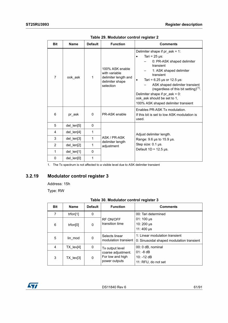
DS11840 Rev 6 61/91
ST25RU3993 Register description
78
3.2.19 Modulator control register 3
Address: 15h
Type: RW
Table 29. Modulator control register 2
Bit Name Default Function Comments
7 ook_ask 1
100% ASK enable with variable delimiter length and delimiter shape selection
Delimiter shape if pr_ask = 1:
• Tari = 25 µs:
– 0: PR-ASK shaped delimiter transient
– 1: ASK shaped delimiter transient
• Tari = 6.25 µs or 12.5 µs:
– ASK shaped delimiter transient (regardless of this bit setting)(1).
Delimiter shape if pr_ask = 0: ook_ask should be set to 1,
100% ASK shaped delimiter transient
1. The Tx spectrum is not affected to a visible level due to ASK delimiter transient
6 pr_ask 0 PR-ASK enableEnables PR-ASK Tx modulation.
If this bit is set to low ASK modulation is used.
5 del_len[5] 0
ASK / PR-ASK delimiter length adjustment
Adjust delimiter length.
Range: 9.6 µs to 15.9 µs.
Step size: 0.1 µs.
Default 1D = 12.5 µs.
4 del_len[4] 1
3 del_len[3] 1
2 del_len[2] 1
1 del_len[1] 0
0 del_len[0] 1
Table 30. Modulator control register 3
Bit Name Default Function Comments
7 trfon[1] 0
RF ON/OFF transition time
00: Tari determined
01: 100 µs
10: 200 µs
11: 400 µs6 trfon[0] 0
5 lin_mod 0Selects linear modulation transient
1: Linear modulation transient
0: Sinusoidal shaped modulation transient
4 TX_lev[4] 0 Tx output level coarse adjustment. For low and high power outputs
00: 0 dB, nominal
01: -8 dB
10: -12 dB
11: RFU, do not set3 TX_lev[3] 0
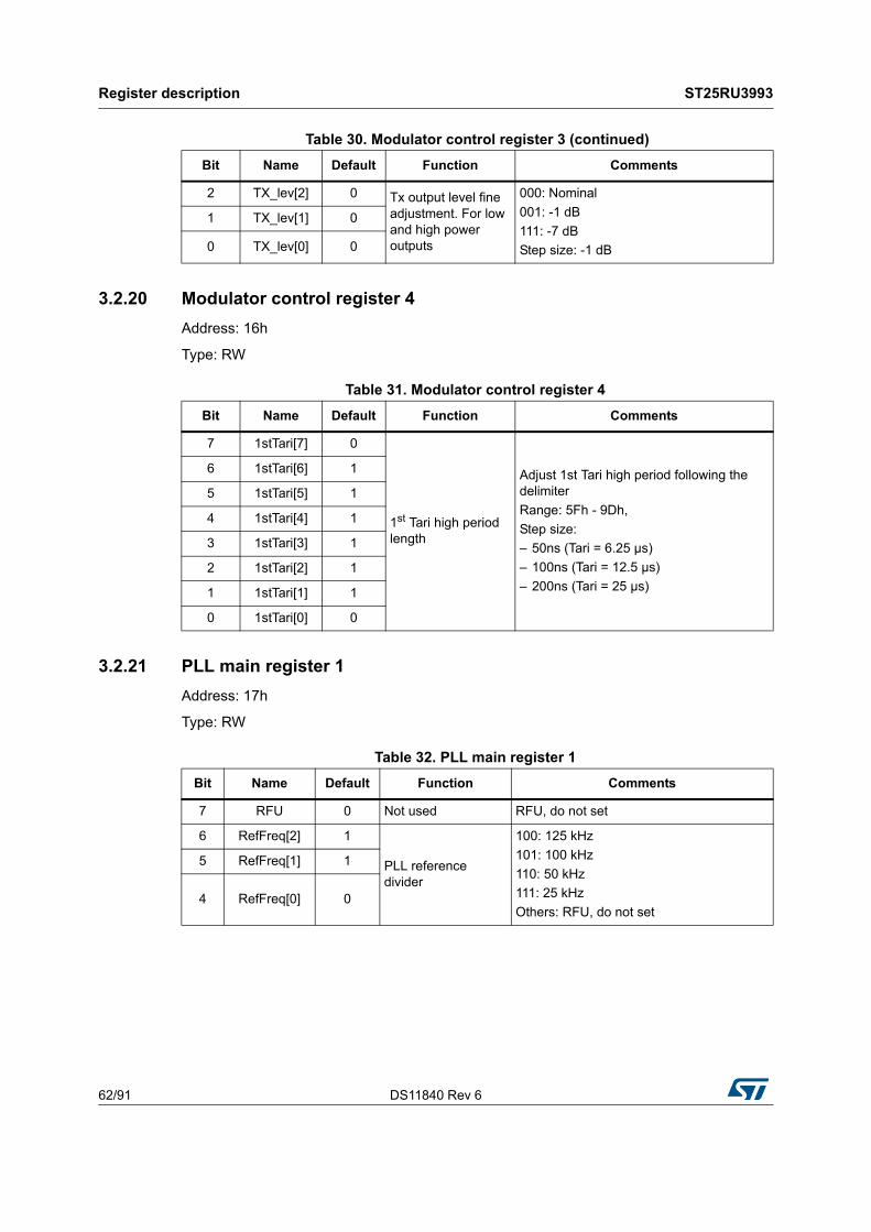
Register description ST25RU3993
62/91 DS11840 Rev 6
3.2.20 Modulator control register 4
Address: 16h
Type: RW
3.2.21 PLL main register 1
Address: 17h
Type: RW
2 TX_lev[2] 0 Tx output level fine adjustment. For low and high power outputs
000: Nominal
001: -1 dB
111: -7 dB
Step size: -1 dB
1 TX_lev[1] 0
0 TX_lev[0] 0
Table 30. Modulator control register 3 (continued)
Bit Name Default Function Comments
Table 31. Modulator control register 4
Bit Name Default Function Comments
7 1stTari[7] 0
1st Tari high period length
Adjust 1st Tari high period following the delimiter
Range: 5Fh - 9Dh,
Step size:
– 50ns (Tari = 6.25 µs)
– 100ns (Tari = 12.5 µs)
– 200ns (Tari = 25 µs)
6 1stTari[6] 1
5 1stTari[5] 1
4 1stTari[4] 1
3 1stTari[3] 1
2 1stTari[2] 1
1 1stTari[1] 1
0 1stTari[0] 0
Table 32. PLL main register 1
Bit Name Default Function Comments
7 RFU 0 Not used RFU, do not set
6 RefFreq[2] 1
PLL reference divider
100: 125 kHz
101: 100 kHz
110: 50 kHz
111: 25 kHz
Others: RFU, do not set
5 RefFreq[1] 1
4 RefFreq[0] 0
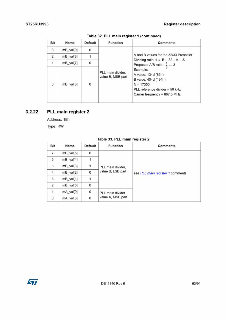
DS11840 Rev 6 63/91
ST25RU3993 Register description
78
3.2.22 PLL main register 2
Address: 18h
Type: RW
3 mB_val[9] 0
PLL main divider, value B, MSB part
A and B values for the 32/33 Prescaler
Dividing ratio:
Proposed A/B ratio: … 3
Example:
A value: 134d (86h)
B value: 404d (194h)
N = 17350
PLL reference divider = 50 kHz
Carrier frequency = 867.5 MHz
2 mB_val[8] 1
1 mB_val[7] 0
0 mB_val[6] 0
Table 32. PLL main register 1 (continued)
Bit Name Default Function Comments
N B 32⋅ A 33⋅+=13---
Table 33. PLL main register 2
Bit Name Default Function Comments
7 mB_val[5] 0
PLL main divider, value B, LSB part see PLL main register 1 comments
6 mB_val[4] 1
5 mB_val[3] 1
4 mB_val[2] 0
3 mB_val[1] 1
2 mB_val[0] 0
1 mA_val[9] 0 PLL main divider value A, MSB part0 mA_val[8] 0
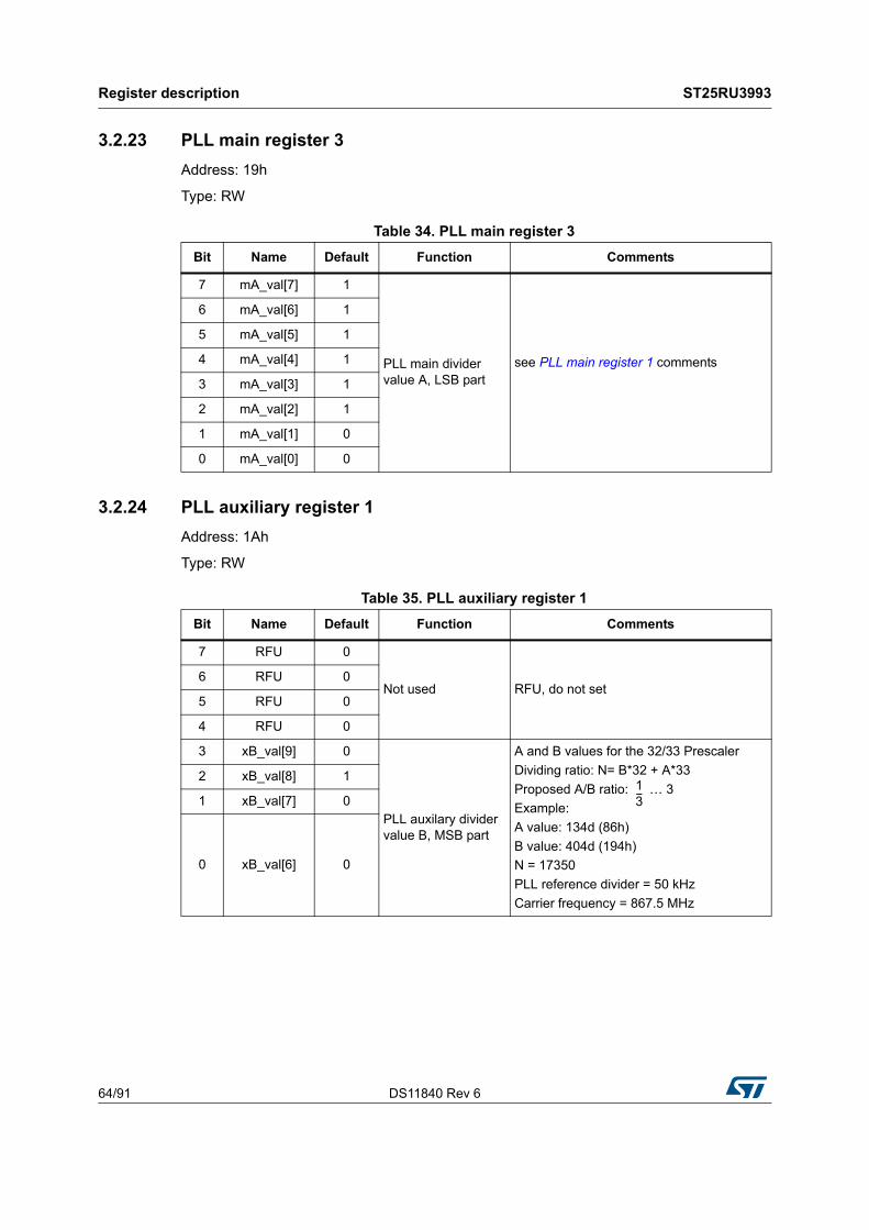
Register description ST25RU3993
64/91 DS11840 Rev 6
3.2.23 PLL main register 3
Address: 19h
Type: RW
3.2.24 PLL auxiliary register 1
Address: 1Ah
Type: RW
Table 34. PLL main register 3
Bit Name Default Function Comments
7 mA_val[7] 1
PLL main divider value A, LSB part
see PLL main register 1 comments
6 mA_val[6] 1
5 mA_val[5] 1
4 mA_val[4] 1
3 mA_val[3] 1
2 mA_val[2] 1
1 mA_val[1] 0
0 mA_val[0] 0
Table 35. PLL auxiliary register 1
Bit Name Default Function Comments
7 RFU 0
Not used RFU, do not set6 RFU 0
5 RFU 0
4 RFU 0
3 xB_val[9] 0
PLL auxilary divider value B, MSB part
A and B values for the 32/33 Prescaler
Dividing ratio: N= B*32 + A*33
Proposed A/B ratio: … 3
Example:
A value: 134d (86h)
B value: 404d (194h)
N = 17350
PLL reference divider = 50 kHz
Carrier frequency = 867.5 MHz
2 xB_val[8] 1
1 xB_val[7] 0
0 xB_val[6] 0
13---
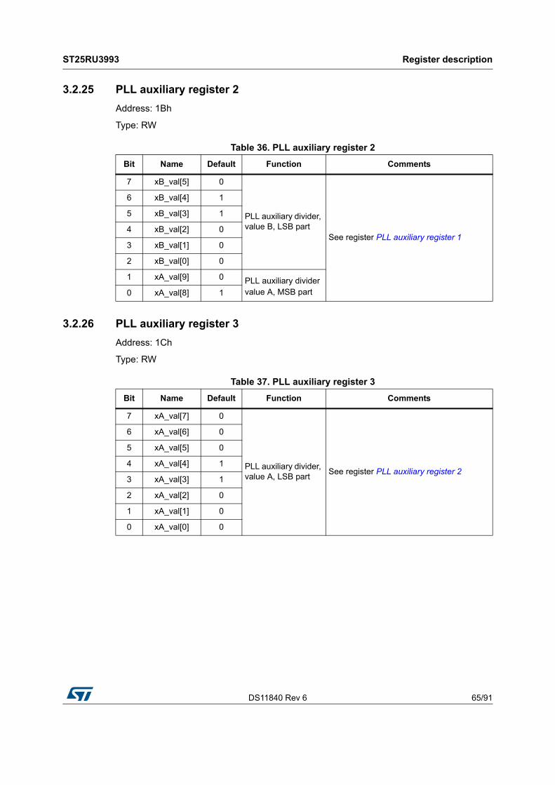
DS11840 Rev 6 65/91
ST25RU3993 Register description
78
3.2.25 PLL auxiliary register 2
Address: 1Bh
Type: RW
3.2.26 PLL auxiliary register 3
Address: 1Ch
Type: RW
Table 36. PLL auxiliary register 2
Bit Name Default Function Comments
7 xB_val[5] 0
PLL auxiliary divider, value B, LSB part
See register PLL auxiliary register 1
6 xB_val[4] 1
5 xB_val[3] 1
4 xB_val[2] 0
3 xB_val[1] 0
2 xB_val[0] 0
1 xA_val[9] 0 PLL auxiliary divider value A, MSB part0 xA_val[8] 1
Table 37. PLL auxiliary register 3
Bit Name Default Function Comments
7 xA_val[7] 0
PLL auxiliary divider, value A, LSB part
See register PLL auxiliary register 2
6 xA_val[6] 0
5 xA_val[5] 0
4 xA_val[4] 1
3 xA_val[3] 1
2 xA_val[2] 0
1 xA_val[1] 0
0 xA_val[0] 0
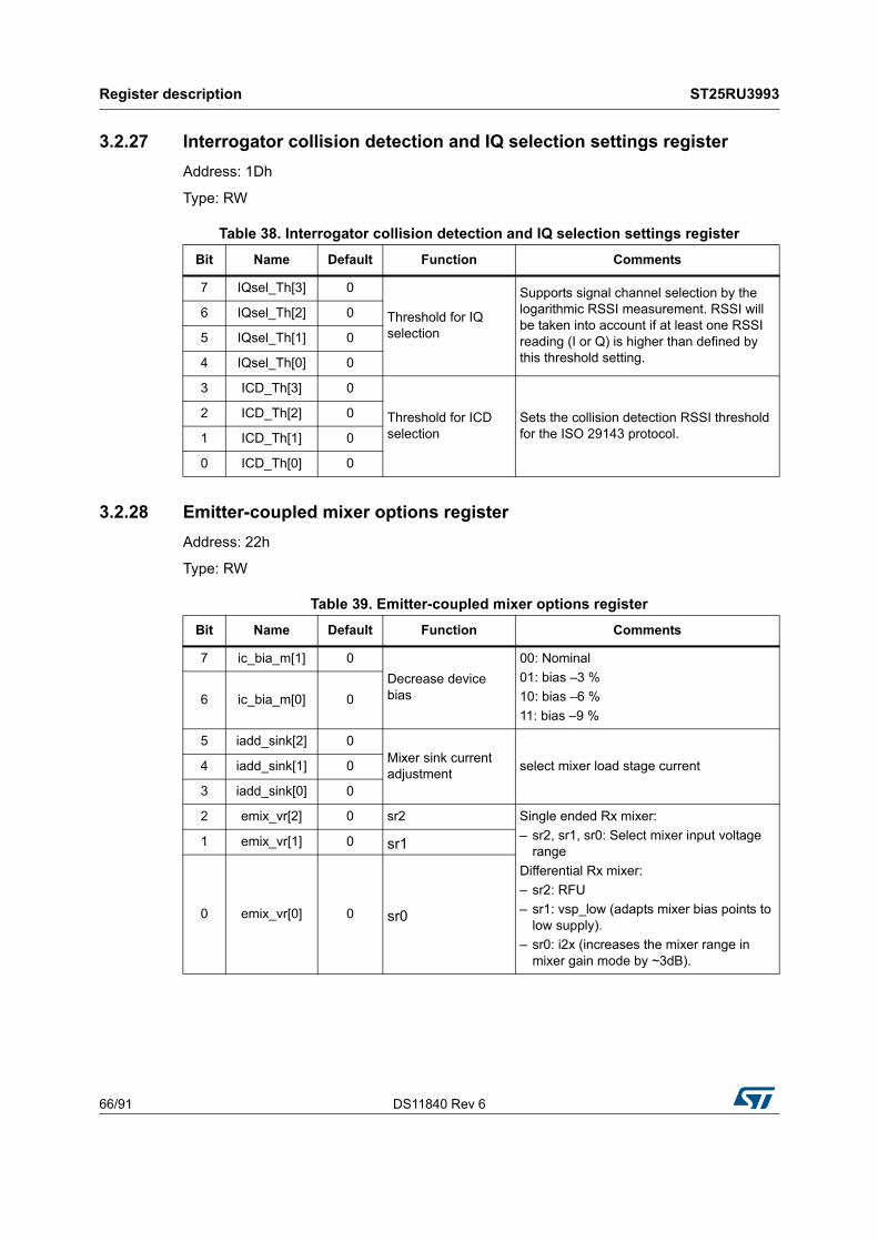
Register description ST25RU3993
66/91 DS11840 Rev 6
3.2.27 Interrogator collision detection and IQ selection settings register
Address: 1Dh
Type: RW
3.2.28 Emitter-coupled mixer options register
Address: 22h
Type: RW
Table 38. Interrogator collision detection and IQ selection settings register
Bit Name Default Function Comments
7 IQsel_Th[3] 0
Threshold for IQ selection
Supports signal channel selection by the logarithmic RSSI measurement. RSSI will be taken into account if at least one RSSI reading (I or Q) is higher than defined by this threshold setting.
6 IQsel_Th[2] 0
5 IQsel_Th[1] 0
4 IQsel_Th[0] 0
3 ICD_Th[3] 0
Threshold for ICD selection
Sets the collision detection RSSI threshold for the ISO 29143 protocol.
2 ICD_Th[2] 0
1 ICD_Th[1] 0
0 ICD_Th[0] 0
Table 39. Emitter-coupled mixer options register
Bit Name Default Function Comments
7 ic_bia_m[1] 0
Decrease device bias
00: Nominal
01: bias –3 %
10: bias –6 %
11: bias –9 %6 ic_bia_m[0] 0
5 iadd_sink[2] 0Mixer sink current adjustment
select mixer load stage current4 iadd_sink[1] 0
3 iadd_sink[0] 0
2 emix_vr[2] 0 sr2 Single ended Rx mixer:
– sr2, sr1, sr0: Select mixer input voltage range
Differential Rx mixer:
– sr2: RFU
– sr1: vsp_low (adapts mixer bias points to low supply).
– sr0: i2x (increases the mixer range in mixer gain mode by ~3dB).
1 emix_vr[1] 0 sr1
0 emix_vr[0] 0 sr0

DS11840 Rev 6 67/91
ST25RU3993 Register description
78
3.3 Status registers
3.3.1 Status readout page setting register
Address: 29h
Type: RW
3.3.2 AGC and internal status display register
Address: 2Ah
Type: R
Table 40. Status readout page setting register
Bit Name Default Function Comments
7 r2Dpage[1] 0 Register page selection for register 2Dh
Defines actual display of ADC readout/regulator setting display register (r2Dpage[1:0] = 01)6 r2Dpage[0] 0
5 r2Cpage[1] 0 Register page selection for register 2Ch
Defines actual display of AGL/VCO/F_CAL/PilotFreq status register (r2Cpage[1:0] = 01)4 r2Cpage[0] 0
3 r2Bpage[3] 0
Register page selection for register 2Bh
0000: Real time RSSI I,Q
0010 : RSSI-0-quiet (noise RSSI), I,Q Quiet level- Acquired by direct command Store RSSI (A8h)
0100: RSSI-1-pilot, I,Q Level at pilot
0110: RSSI-2-data, I,Q Level at 2nd byte
1000: RSSI-3-peak, I, Q Peak Level
1100: IDC-Time - Time at exceeding threshold.
1101: IDC-Length - Threshold exceeding duration.
1110: Err-Time - Time at first protocol violation. Time is in terms of received bits.
Others: not used
2 r2Bpage[2] 0
1 r2Bpage[1] 0
0 r2Bpage[0] 0
Table 41. AGC and internal status display register
Bit Name Function Comments
7 subc_phase Sub-carrier phase0: Sub-carriers are in anti-phase
1: Sub-carriers are in phase
6 agc[2]
AGC statusSteps: 7
Step size: 3 dB5 agc[1]
4 agc[0]
3 in_select
Shows the source of the sub-carrier signal that is used for decoding
0: I-Channel
1: Q-Channel
Value is valid from reception start until the start of the next transmission

Register description ST25RU3993
68/91 DS11840 Rev 6
3.3.3 RSSI display register
Address: 2Bh
Type: R
3.3.4 AGL/VCO/F_CAL/PilotFreq status display register (r2Cpage[1:0] = 00)
Address: 2Ch, r2Cpage[1:0] = 00
Type: R
2 rf_ok RF level stable Indicates that the RF carrier is stable
1 pll_ok PLL locked Indicates that PLL is locked to the RF carrier
0 osc_ok Crystal oscillator stableIndicates that the reference oscillator frequency is stable
Table 41. AGC and internal status display register (continued)
Bit Name Function Comments
Table 42. RSSI display register
Bit Name Function Comments
7 rssi[7] RSSI value of Q channel. The RSSI type defined in AGC and internal status display register, bits r2Bpage[3:0].
Displays the signal strength of the Q signal channel
Steps: 16
Step size: 2 dB
6 rssi[6]
5 rssi[5]
4 rssi[4]
3 rssi[3] RSSI value of I channel. The RSSI type defined in Status readout page setting register, bits r2Bpage[3:0].
Displays the signal strength of the I signal channel
Steps: 16
Step size: 2 dB
2 rssi[2]
1 rssi[1]
0 rsss[0]
Table 43. AGL/VCO/F_CAL/PilotFreq status display register (r2Cpage[1:0] = 00)
Bit Name Function Comments
7 RFU Not used Status bit, read as 0
6 RFU Not used Status bit, read as 0
5 agl[5]AGL status of Q channel Available steps are 0, 1, 2, 3, 4
Step size: 3 dB
Range: 0 dB – 12 dB
Steps 5, 6, 7 have no action
4 agl[4]
3 agl[3]
2 agl[2]
AGL status of I channel1 agl[1]
0 agl[0]

DS11840 Rev 6 69/91
ST25RU3993 Register description
78
3.3.5 AGL/VCO/F_CAL/PilotFreq status register (r2Cpage[1:0] = 01)
Address: 2Ch, r2Cpage[1:0] = 01
Type: R
3.3.6 AGL/VCO/F_CAL/PilotFreq status register (r2Cpage[1:0] = 10)
Address: 2Ch, r2Cpage[1:0] = 10
Type: R
Table 44. AGL/VCO/F_CAL/PilotFreq status register (r2Cpage[1:0] = 01)
Bit Name Function Comments
7 vco_ri[7]
VCO automatic range select result
Displays the result of the internal VCO automatic range selection procedure.
Steps: 16
6 vco_ri[6]
5 vco_ri[5]
4 vco_ri[4]
3 vco_ri[3] Set to logic 1 RFU, read as 1
2 vco_ri[2]
VCO pin voltage measurement result
Displays the result of the internal VCO measurement.
Steps: 7
Range: 0 V to VDD_A
1 vco_ri[1]
0 vco_ri[0]
Table 45. AGL/VCO/F_CAL/PilotFreq status register (r2Cpage[1:0] = 10)
Bit Name Function Comments
7 hp_cal[3]
High pass calibration data
Steps: 16
Step size: 4%
6 hp_cal[2]
5 hp_cal[1]
4 hp_cal[0]
3 lp_cal[3]
Low pass calibration data
Steps: 16
Step size: 4%
2 lp_cal[2]
1 lp_cal[1]
0 lp_cal[0]
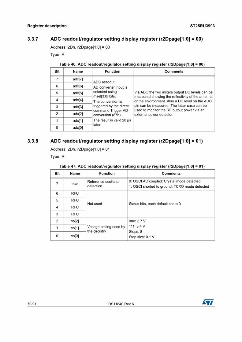
Register description ST25RU3993
70/91 DS11840 Rev 6
3.3.7 ADC readout/regulator setting display register (r2Dpage[1:0] = 00)
Address: 2Dh, r2Dpage[1:0] = 00
Type: R
3.3.8 ADC readout/regulator setting display register (r2Dpage[1:0] = 01)
Address: 2Dh, r2Dpage[1:0] = 01
Type: R
Table 46. ADC readout/regulator setting display register (r2Dpage[1:0] = 00)
Bit Name Function Comments
7 adc[7]ADC readout.
AD converter input is selected using msel[3:0] bits.
The conversion is triggered by the direct command Trigger AD conversion (87h).
The result is valid 20 µs later.
Via ADC the two mixers output DC levels can be measured showing the reflectivity of the antenna or the environment. Also a DC level on the ADC pin can be measured. The latter case can be used to monitor the RF output power via an external power detector.
6 adc[6]
5 adc[5]
4 adc[4]
3 adc[3]
2 adc[2]
1 adc[1]
0 adc[0]
Table 47. ADC readout/regulator setting display register (r2Dpage[1:0] = 01)
Bit Name Function Comments
7 tcxoReference oscillator detection
0: OSCI AC coupled: Crystal mode detected
1: OSCI shorted to ground: TCXO mode detected
6 RFU
Not used Status bits, each default set to 05 RFU
4 RFU
3 RFU
2 vs[2]
Voltage setting used by the circuitry
000: 2.7 V
111: 3.4 V
Steps: 8
Step size: 0.1 V
1 vs[1]
0 vs[0]
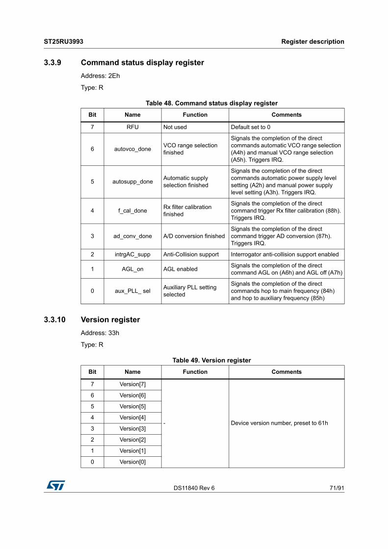
DS11840 Rev 6 71/91
ST25RU3993 Register description
78
3.3.9 Command status display register
Address: 2Eh
Type: R
3.3.10 Version register
Address: 33h
Type: R
Table 48. Command status display register
Bit Name Function Comments
7 RFU Not used Default set to 0
6 autovco_doneVCO range selection finished
Signals the completion of the direct commands automatic VCO range selection (A4h) and manual VCO range selection (A5h). Triggers IRQ.
5 autosupp_doneAutomatic supply selection finished
Signals the completion of the direct commands automatic power supply level setting (A2h) and manual power supply level setting (A3h). Triggers IRQ.
4 f_cal_doneRx filter calibration finished
Signals the completion of the direct command trigger Rx filter calibration (88h). Triggers IRQ.
3 ad_conv_done A/D conversion finishedSignals the completion of the direct command trigger AD conversion (87h). Triggers IRQ.
2 intrgAC_supp Anti-Collision support Interrogator anti-collision support enabled
1 AGL_on AGL enabledSignals the completion of the direct command AGL on (A6h) and AGL off (A7h)
0 aux_PLL_ selAuxiliary PLL setting selected
Signals the completion of the direct commands hop to main frequency (84h) and hop to auxiliary frequency (85h)
Table 49. Version register
Bit Name Function Comments
7 Version[7]
- Device version number, preset to 61h
6 Version[6]
5 Version[5]
4 Version[4]
3 Version[3]
2 Version[2]
1 Version[1]
0 Version[0]
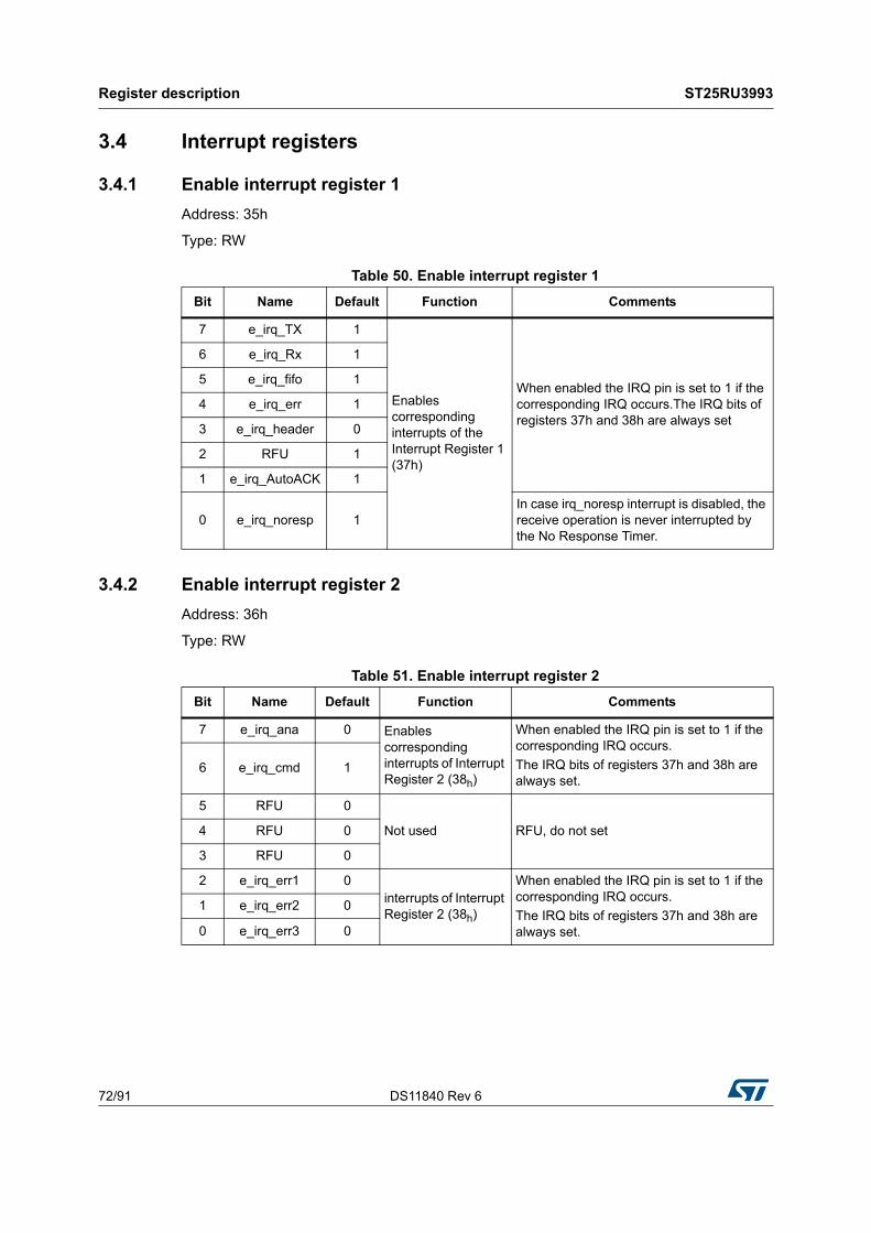
Register description ST25RU3993
72/91 DS11840 Rev 6
3.4 Interrupt registers
3.4.1 Enable interrupt register 1
Address: 35h
Type: RW
3.4.2 Enable interrupt register 2
Address: 36h
Type: RW
Table 50. Enable interrupt register 1
Bit Name Default Function Comments
7 e_irq_TX 1
Enables corresponding interrupts of the Interrupt Register 1 (37h)
When enabled the IRQ pin is set to 1 if the corresponding IRQ occurs.The IRQ bits of registers 37h and 38h are always set
6 e_irq_Rx 1
5 e_irq_fifo 1
4 e_irq_err 1
3 e_irq_header 0
2 RFU 1
1 e_irq_AutoACK 1
0 e_irq_noresp 1In case irq_noresp interrupt is disabled, the receive operation is never interrupted by the No Response Timer.
Table 51. Enable interrupt register 2
Bit Name Default Function Comments
7 e_irq_ana 0 Enables corresponding interrupts of Interrupt Register 2 (38h)
When enabled the IRQ pin is set to 1 if the corresponding IRQ occurs.
The IRQ bits of registers 37h and 38h are always set.
6 e_irq_cmd 1
5 RFU 0
Not used RFU, do not set4 RFU 0
3 RFU 0
2 e_irq_err1 0interrupts of Interrupt Register 2 (38h)
When enabled the IRQ pin is set to 1 if the corresponding IRQ occurs.
The IRQ bits of registers 37h and 38h are always set.
1 e_irq_err2 0
0 e_irq_err3 0

DS11840 Rev 6 73/91
ST25RU3993 Register description
78
3.4.3 Interrupt register 1
Address: 37h
Type: R
Note: The content of this register is set to 0 at power up and when EN = low. It is automatically reset at the end of a read phase. A reset also removes the IRQ flag.
Table 52. Interrupt register 1
Bit Name Function Comments
7 Irq_TX IRQ due to the end of TxAn interrupt is generated when Tx is finished.
6 Irq_RxIRQ due to the end of Rx
An interrupt is generated when Rx is finished.
5 Irq_fifo FIFO fill levelLess than 6 bytes in FIFO during Tx or more than 18 bytes in FIFO during Rx
4 Irq_err IRQ set due to an error Signaling a reception or transmission error
3Irq_header / Irq_2nd_byte
Header bit / 2nd byteReceived header bit is high /
Two bytes already in the FIFO – if fifo_dir_irq2 = 1 (Register 1Ah)
2 RFU Not Used -
1 Irq_AutoACK Auto ACK finished
AutoACK is finished.
Bit is set to 1 in the following cases:
The AutoACK procedure was successfully finished.
In the AutoACK procedure the ACK command was sent and the procedure was terminated due to a No Response IRQ.
In the AutoACK procedure the ACK command was sent and procedure was terminated due to a reception error.
0 Irq_noresp No response interruptSignals the MCU that the no response timer expired, it also interrupts receive operation.
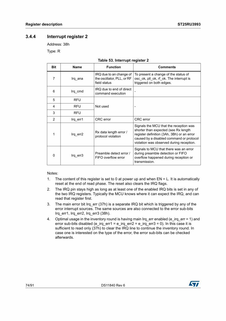
Register description ST25RU3993
74/91 DS11840 Rev 6
3.4.4 Interrupt register 2
Address: 38h
Type: R
Notes:
1. The content of this register is set to 0 at power up and when EN = L. It is automatically reset at the end of read phase. The reset also clears the IRQ flags.
2. The IRQ pin stays high as long as at least one of the enabled IRQ bits is set in any of the two IRQ registers. Typically the MCU knows where it can expect the IRQ, and can read that register first.
3. The main error bit Irq_err (37h) is a separate IRQ bit which is triggered by any of the error interrupt sources. The same sources are also connected to the error sub-bits Irq_err1, Irq_err2, Irq_err3 (38h).
4. Optimal usage in the inventory round is having main Irq_err enabled (e_irq_err = 1) and error sub-bits disabled (e_irq_err1 = e_irq_err2 = e_irq_err3 = 0). In this case it is sufficient to read only (37h) to clear the IRQ line to continue the inventory round. In case one is interested on the type of the error, the error sub-bits can be checked afterwards.
Table 53. Interrupt register 2
Bit Name Function Comments
7 Irq_anaIRQ due to an change of the oscillator, PLL, or RF field status
To present a change of the status of osc_ok, pll_ok, rf_ok. The interrupt is triggered on both edges.
6 Irq_cmdIRQ due to end of direct command execution
-
5 RFU
Not used -4 RFU
3 RFU
2 Irq_err1 CRC error CRC error
1 Irq_err2Rx data length error / protocol violation
Signals the MCU that the reception was shorter than expected (see Rx length register definition (3Ah, 3Bh) or an error caused by a disabled command or protocol violation was observed during reception.
0 Irq_err3 Preamble detect error / FIFO overflow error
Signals to MCU that there was an error during preamble detection or FIFO overflow happened during reception or transmission.

DS11840 Rev 6 75/91
ST25RU3993 Register description
78
3.5 Communication registers
3.5.1 FIFO status register
Address: 39h
Type: R
3.5.2 Rx length register 1
Address: 3Ah
Type: RW
Table 54. FIFO status register
Bit Name Function Comments
7 TX_status Tx status1: Shows that a data transmission is in progress.
6 Rx_status Rx status1: Shows that a data reception is in progress.
5 Fovfl FIFO overflow 1: More than 24 bytes were loaded to one of the FIFOs
4 Fb[4]
FIFO bytes
Number of bytes loaded in FIFO that has not been read out yet. In case an empty FIFO is read out the value 1Fh is displayed in the Fb[4:0] bits.
3 Fb[3]
2 Fb[2]
1 Fb[1]
0 Fb[0]
Table 55. Rx length register 1
Bit Name Default Function Comments
7 Rx_crc_n2 0Receiving without CRC
Temporary receiving without CRC.
6 fifo_dir_irq2 0Direct FIFO and 2nd byte IRQ
All bytes including CRC are transferred to FIFO, irq_header is changed to irq_2ndbyte. For PC+EPC manual reception length setting.
5 rep_irq2 0 Repeat 2nd byte IRQ
Enables IRQ after 4th, 6th… received byte. Bit can be set to 0 during reception when additional IRQs are not required. The aim is to support XPC words.

Register description ST25RU3993
76/91 DS11840 Rev 6
3.5.3 Rx length register 2
Address: 3Bh
Type: RW
3.5.4 Tx setting register
Address: 3Ch
Type: RW
4 auto_errcode_Rxl 0Automatic tag error code Rx length preset
In case received header bit is set to 1, the Rx length is automatically changed to the tag error code length (41bits).
Used to change the previously expected Rx length information when a tag transmits the error code instead of a normal response.
3 Rxl[11] 0
Rx length MSB part -2 Rxl[10] 0
1 Rxl[9] 0
0 Rxl[8] 0
Table 55. Rx length register 1 (continued)
Bit Name Default Function Comments
Table 56. Rx length register 2
Bit Name Default Function Comments
7 Rxl[7] 0
Rx length LSB part, number of bits
In case short direct commands are used the register is automatically preset to correct expected reception length.
16 bits are expected for commands 98h, 99h, 9Ah, 9Bh, 9Ch; 32 bits are expected for the direct command 9Fh.
In other cases the host system should set the expected length.
6 Rxl[6] 0
5 Rxl[5] 0
4 Rxl[4] 0
3 Rxl[3] 0
2 Rxl[2] 0
1 Rxl[1] 0
0 Rxl[0] 0
Table 57. Tx setting register
Bit Name Default Function Comments
7 RFU 0
Not used RFU, do not set6 RFU 0
5 RFU 0
4 RFU 0

DS11840 Rev 6 77/91
ST25RU3993 Register description
78
3.5.5 Tx length register 1
Address: 3Dh
Type: RW
3.5.6 Tx length register 2
Address: 3Eh
Type: RW
3 TXCRC_5 0 Tx CRC type0: CRC-16 1: CRC-5
2 Force_TRcal 0TRcal period in normal transmission
Normally TRcal is automatically transmitted when the direct command Query (98h), according to EPC Gen2 and ISO18000-6C, is issued.
In case Force_TRcal = 1 the TRcal period is transmitted also in normal data transmission (direct commands 90h, 91h)
1 S1 0Session bits
Used for Gen 2 direct commands Query (98h).0 S0 0
Table 57. Tx setting register (continued)
Bit Name Default Function Comments
Table 58. Tx length register 1
Bit Name Default Function Comments
7 TXl[11] 0
Tx length high nibble
High and mid nibbles of complete bytes being transmitted through the FIFO
6 TXl[10] 0
5 TXl[9] 0
4 TXl[8] 0
3 TXl[7] 0
Tx length mid nibble2 TXl[6] 0
1 TXl[5] 0
0 TXl[4] 0
Table 59. Tx length register 2
Bit Name Default Function Comments
7 TXl[3] 0
Tx length low nibbleLow nibbles of complete bytes being transmitted through the FIFO
6 TXl[2] 0
5 TXl[1] 0
4 TXl[0] 0
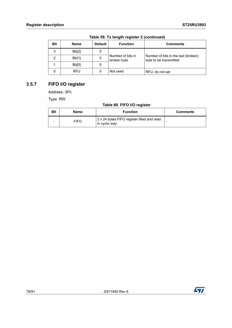
Register description ST25RU3993
78/91 DS11840 Rev 6
3.5.7 FIFO I/O register
Address: 3Fh
Type: RW
3 Bb[2] 0Number of bits in broken byte
Number of bits in the last (broken) byte to be transmitted
2 Bb[1] 0
1 Bb[0] 0
0 RFU 0 Not used RFU, do not set
Table 59. Tx length register 2 (continued)
Bit Name Default Function Comments
Table 60. FIFO I/O register
Bit Name Function Comments
- FIFO2 x 24 bytes FIFO register filled and read in cyclic way
-
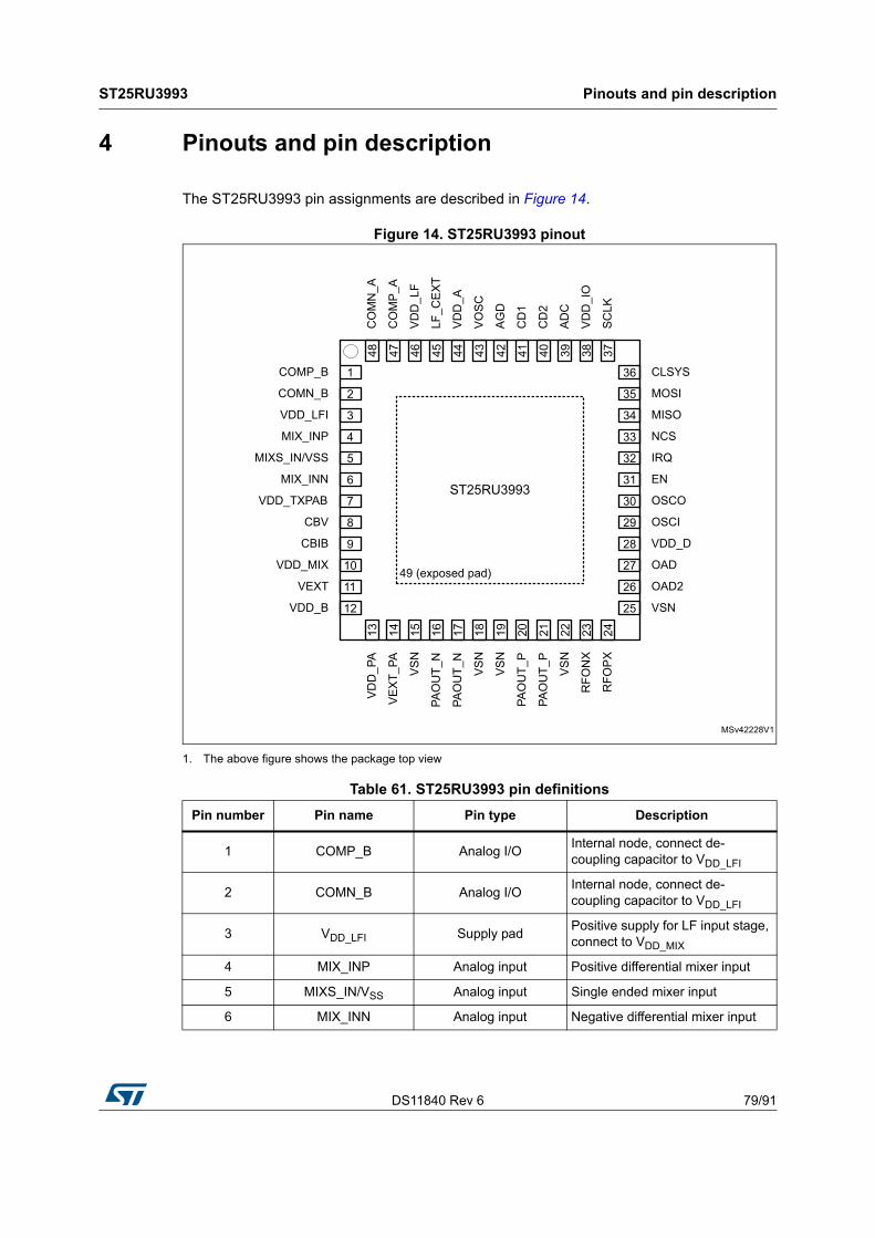
DS11840 Rev 6 79/91
ST25RU3993 Pinouts and pin description
81
4 Pinouts and pin description
The ST25RU3993 pin assignments are described in Figure 14.
Figure 14. ST25RU3993 pinout
1. The above figure shows the package top view
Table 61. ST25RU3993 pin definitions
Pin number Pin name Pin type Description
1 COMP_B Analog I/OInternal node, connect de-coupling capacitor to VDD_LFI
2 COMN_B Analog I/OInternal node, connect de-coupling capacitor to VDD_LFI
3 VDD_LFI Supply padPositive supply for LF input stage, connect to VDD_MIX
4 MIX_INP Analog input Positive differential mixer input
5 MIXS_IN/VSS Analog input Single ended mixer input
6 MIX_INN Analog input Negative differential mixer input

Pinouts and pin description ST25RU3993
80/91 DS11840 Rev 6
7 VDD_TXPAB Supply padBias positive supply. Connect to VDD_MIX
8 CBV Analog I/OInternal node, connect de-coupling capacitor to VDD_MIX
9 CBIB Analog I/OInternal node, connect de-coupling capacitor to ground
10 VDD_MIX Analog I/OMixer positive supply, internally regulated
11 VEXT Supply padMain positive supply input, input to regulators
12 VDD_B Analog I/OBuffer positive supply, internally regulated
13 VDD_PA Analog I/OPA positive supply, internally regulated
14 VEXT_PA Supply pad PA positive supply regulator input
15 VSN Supply pad Negative supply
16 PAOUT_N Analog output Negative PA RF output
17 PAOUT_N Analog output Negative PA RF output
18 VSN Supply pad Negative supply
19 VSN Supply pad Negative supply
20 PAOUT_P Analog output Positive PA RF output
21 PAOUT_P Analog output Positive PA RF output
22 VSN Supply pad Negative supply
23 RFONX Analog outputlow-power linear negative RF output (~0dBm)
24 RFOPX Analog outputlow-power linear positive RF output (~0dBm)
25 VSN Supply pad Negative supply
26 OAD2 Analog I/OAnalog or digital received signal output
27 OAD Analog I/OAnalog or digital received signal output
28 VDD_D Analog I/OPositive supply for logic, internally regulated
29 OSCI Analog inputCrystal oscillator input or short to ground if external TCXO is used
30 OSCO Analog I/OCrystal oscillator output or external 20MHz clock input
31 EN Digital input Enable input
32 IRQ Digital output Interrupt request output
Table 61. ST25RU3993 pin definitions
Pin number Pin name Pin type Description
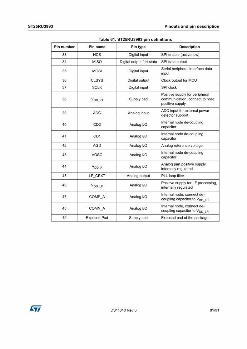
DS11840 Rev 6 81/91
ST25RU3993 Pinouts and pin description
81
33 NCS Digital input SPI enable (active low)
34 MISO Digital output / tri-state SPI data output
35 MOSI Digital inputSerial peripheral interface data input
36 CLSYS Digital output Clock output for MCU
37 SCLK Digital input SPI clock
38 VDD_IO Supply padPositive supply for peripheral communication, connect to host positive supply.
39 ADC Analog inputADC input for external power detector support
40 CD2 Analog I/OInternal node de-coupling capacitor
41 CD1 Analog I/OInternal node de-coupling capacitor
42 AGD Analog I/O Analog reference voltage
43 VOSC Analog I/OInternal node de-coupling capacitor
44 VDD_A Analog I/OAnalog part positive supply, internally regulated
45 LF_CEXT Analog output PLL loop filter
46 VDD_LF Analog I/OPositive supply for LF processing, internally regulated
47 COMP_A Analog I/OInternal node, connect de-coupling capacitor to VDD_LFI
48 COMN_A Analog I/OInternal node, connect de-coupling capacitor to VDD_LFI
49 Exposed Pad Supply pad Exposed pad of the package
Table 61. ST25RU3993 pin definitions
Pin number Pin name Pin type Description
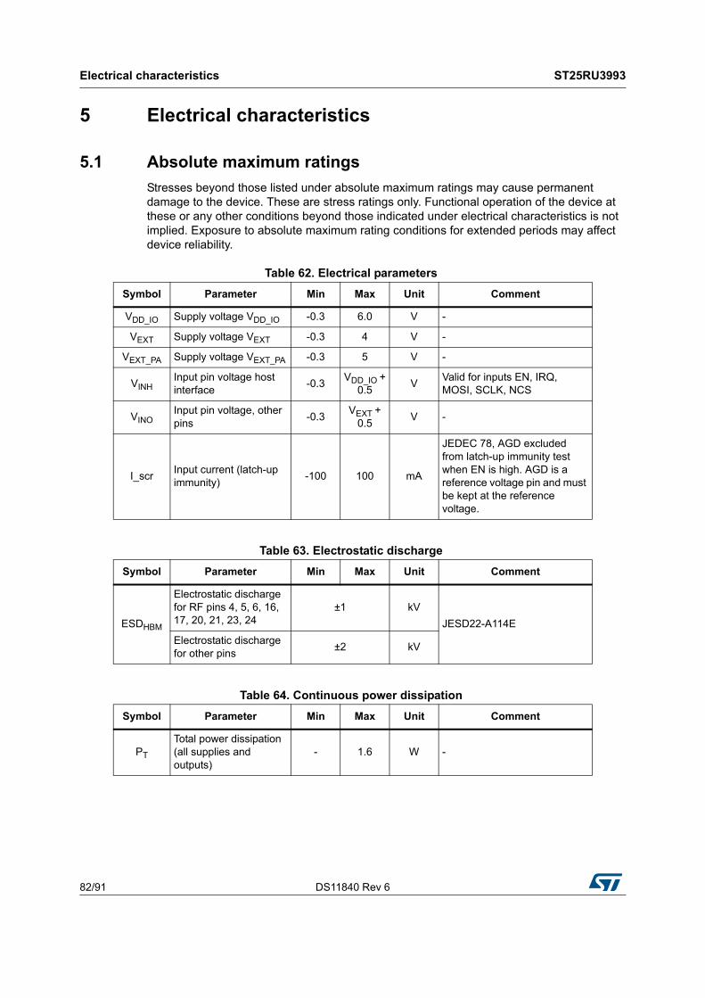
Electrical characteristics ST25RU3993
82/91 DS11840 Rev 6
5 Electrical characteristics
5.1 Absolute maximum ratings
Stresses beyond those listed under absolute maximum ratings may cause permanent damage to the device. These are stress ratings only. Functional operation of the device at these or any other conditions beyond those indicated under electrical characteristics is not implied. Exposure to absolute maximum rating conditions for extended periods may affect device reliability.
Table 62. Electrical parameters
Symbol Parameter Min Max Unit Comment
VDD_IO Supply voltage VDD_IO -0.3 6.0 V -
VEXT Supply voltage VEXT -0.3 4 V -
VEXT_PA Supply voltage VEXT_PA -0.3 5 V -
VINHInput pin voltage host interface
-0.3VDD_IO +
0.5V
Valid for inputs EN, IRQ, MOSI, SCLK, NCS
VINOInput pin voltage, other pins
-0.3VEXT +
0.5V -
I_scrInput current (latch-up immunity)
-100 100 mA
JEDEC 78, AGD excluded from latch-up immunity test when EN is high. AGD is a reference voltage pin and must be kept at the reference voltage.
Table 63. Electrostatic discharge
Symbol Parameter Min Max Unit Comment
ESDHBM
Electrostatic discharge for RF pins 4, 5, 6, 16, 17, 20, 21, 23, 24
±1 kV
JESD22-A114E
Electrostatic discharge for other pins
±2 kV
Table 64. Continuous power dissipation
Symbol Parameter Min Max Unit Comment
PT
Total power dissipation (all supplies and outputs)
- 1.6 W -

DS11840 Rev 6 83/91
ST25RU3993 Electrical characteristics
86
5.2 Operating conditions
All limits are guaranteed. The parameters with min and max values are guaranteed with production tests or SQC (Statistical Quality Control) methods.
VEXT = 3.3 V, VEXT_PA = 3.3 V, VDD_IO = 3.3 V, TAMB = 25 ºC unless otherwise noted.
Table 65. Temperature ranges and storage conditions
Symbol Parameter Min Max Unit Comment
TJ
Maximum operating virtual junction temperature
- 120 °C -
Tstrg Storage temperature -55 125 °C -
TbodyPackage body temperature
- 260 °C
IPC/JEDEC J-STD-020. The reflow peak soldering temperature (body temperature) is specified according IPC/JEDEC J-STD-020 “Moisture/Reflow Sensitivity Classification for Non-hermetic Solid State Surface Mount Devices. The lead finish for Pb-free leaded packages is “Matte Tin” (100% Sn).
RHNCRelative humidity (non condensing)
5 85 % -
MSLMoisture sensitivity level
3 -Represents a max. floor life time of 168h
Table 66. Operating conditions
Symbol Parameter Conditions Min Typ Max Unit
IEXT
Supply current without VDD_PA current
VEXT consumption 65(1) 75 - mA
IEXT_PASupply current for internal PA
VDD_PA = 3 Vpa_bias[1:0] = 00bTX_lev[4:0] = 0 dBeTX[3:2] = 00b
- 120 -
mAVDD_PA = 3 Vpa_bias[1:0] = 01bTX_lev[4:0] = 0 dBeTX[3:2] = 00b
- 180 -
ISTBYSupply current in standby mode
- - 3 - mA

Electrical characteristics ST25RU3993
84/91 DS11840 Rev 6
IPDSupply current in power-down mode
All system disabled including supply voltage regulators
- 1 10 μA
VAGD AGD voltage - 1.45 1.55 1.65 V
VPORPower-on reset voltage (POR)
- 1 1.8 2.0 V
VRD Regulator drop (2) - 300 - mV
VDD_PARegulated supply for internal PA
- - 3 - V
PPSSR
Rejection of external supply noise on the supply regulator
(3) - 26 - dB
PRFAUXAuxiliary RF output power
VDD_B =3 V - 0 - dBm
PPAOUTInternal PA output power
VDD_PA = 3 V
pa_bias[1:0] = 00bTX_lev[4:0] = 0 dB
eTX[3:2] = 00b
- 17 -
dBmVDD_PA = 3 V
pa_bias[1:0] = 01bTX_lev[4:0] = 0 dB
eTX[3:2] = 00b
- 20 -
1. Using ic_bia_m[1:0] option bits, the consumption can be decreased up to 9%. The drawback of decreased power consumption can be higher noise, lower output power, and declining sensitivity.
2. After execution of direct command: Automatic Power Supply Level Setting (A2h).
3. The difference between the external supply and the regulated voltage is higher than 300mV.
Table 67. Differential mixer
Symbol Parameter Conditions Min Typ Max Unit
RRFIN_DIFFDiff. mixer input impedance
- - 100 - Ω
VSENS_NOM_
DIFF
Nominal diff. mixer input sensitivity
Nominal diff. mixer setting,
PER=0.1%- -67 - dBm
VSENS_GAIN_
DIFF
Increased diff. mixer input sensitivity
Increased diff. mixer gain,
PER=0.1%- -77 - dBm
VSENS_LBT_
DIFF
Diff. mixer LBT sensitivity
Maximum diff. mixer LBT sensitivity
- -90 - dBm
IP3DIFFDiff. mixer third order intercept point
Nominal diff. mixer setting
VEXT = 3 V- 20 - dBm
Table 66. Operating conditions (continued)
Symbol Parameter Conditions Min Typ Max Unit
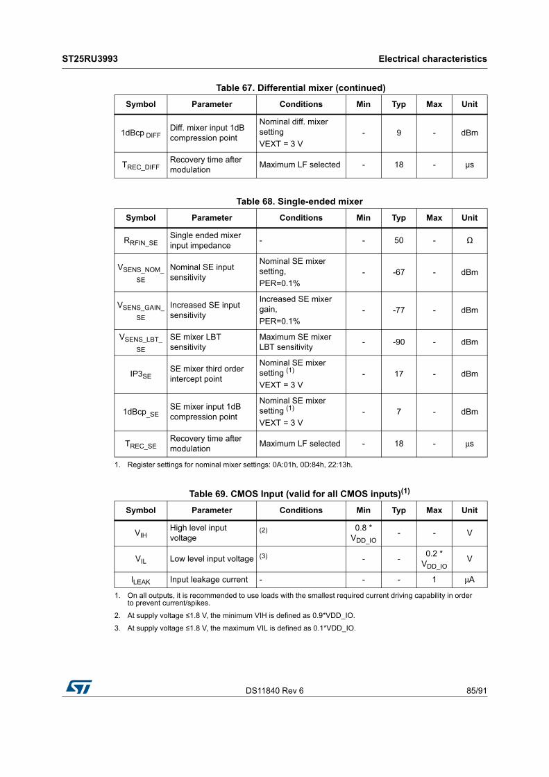
DS11840 Rev 6 85/91
ST25RU3993 Electrical characteristics
86
1dBcp DIFFDiff. mixer input 1dB compression point
Nominal diff. mixer setting
VEXT = 3 V- 9 - dBm
TREC_DIFFRecovery time after modulation
Maximum LF selected - 18 - μs
Table 68. Single-ended mixer
Symbol Parameter Conditions Min Typ Max Unit
RRFIN_SESingle ended mixer input impedance
- - 50 - Ω
VSENS_NOM_
SE
Nominal SE input sensitivity
Nominal SE mixer setting,
PER=0.1%- -67 - dBm
VSENS_GAIN_
SE
Increased SE input sensitivity
Increased SE mixer gain,
PER=0.1%- -77 - dBm
VSENS_LBT_
SE
SE mixer LBT sensitivity
Maximum SE mixer LBT sensitivity
- -90 - dBm
IP3SESE mixer third order intercept point
Nominal SE mixer setting (1)
VEXT = 3 V
1. Register settings for nominal mixer settings: 0A:01h, 0D:84h, 22:13h.
- 17 - dBm
1dBcp_SESE mixer input 1dB compression point
Nominal SE mixer setting (1)
VEXT = 3 V- 7 - dBm
TREC_SERecovery time after modulation
Maximum LF selected - 18 - μs
Table 69. CMOS Input (valid for all CMOS inputs)(1)
1. On all outputs, it is recommended to use loads with the smallest required current driving capability in order to prevent current/spikes.
Symbol Parameter Conditions Min Typ Max Unit
VIHHigh level input voltage
(2)
2. At supply voltage ≤1.8 V, the minimum VIH is defined as 0.9*VDD_IO.
0.8 * VDD_IO
- - V
VIL Low level input voltage (3)
3. At supply voltage ≤1.8 V, the maximum VIL is defined as 0.1*VDD_IO.
- -0.2 *
VDD_IO V
lLEAK Input leakage current - - - 1 μA
Table 67. Differential mixer (continued)
Symbol Parameter Conditions Min Typ Max Unit
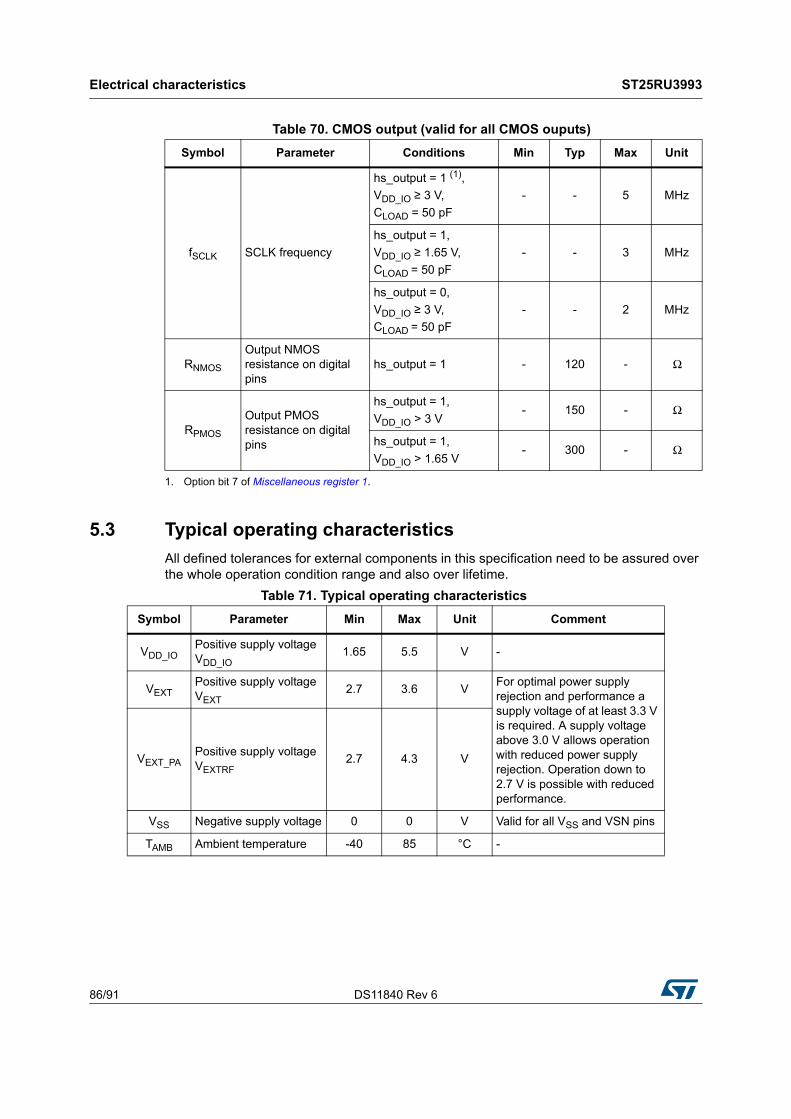
Electrical characteristics ST25RU3993
86/91 DS11840 Rev 6
5.3 Typical operating characteristics
All defined tolerances for external components in this specification need to be assured over the whole operation condition range and also over lifetime.
Table 70. CMOS output (valid for all CMOS ouputs)
Symbol Parameter Conditions Min Typ Max Unit
fSCLK SCLK frequency
hs_output = 1 (1),
VDD_IO ≥ 3 V,
CLOAD = 50 pF
1. Option bit 7 of Miscellaneous register 1.
- - 5 MHz
hs_output = 1,
VDD_IO ≥ 1.65 V,
CLOAD = 50 pF
- - 3 MHz
hs_output = 0,
VDD_IO ≥ 3 V,
CLOAD = 50 pF
- - 2 MHz
RNMOS
Output NMOS resistance on digital pins
hs_output = 1 - 120 - Ω
RPMOS
Output PMOS resistance on digital pins
hs_output = 1,
VDD_IO > 3 V- 150 - Ω
hs_output = 1,
VDD_IO > 1.65 V- 300 - Ω
Table 71. Typical operating characteristics
Symbol Parameter Min Max Unit Comment
VDD_IOPositive supply voltage VDD_IO
1.65 5.5 V -
VEXTPositive supply voltage VEXT
2.7 3.6 VFor optimal power supply rejection and performance a supply voltage of at least 3.3 V is required. A supply voltage above 3.0 V allows operation with reduced power supply rejection. Operation down to 2.7 V is possible with reduced performance.
VEXT_PAPositive supply voltage VEXTRF
2.7 4.3 V
VSS Negative supply voltage 0 0 V Valid for all VSS and VSN pins
TAMB Ambient temperature -40 85 °C -

DS11840 Rev 6 87/91
ST25RU3993 Package information
88
6 Package information
In order to meet environmental requirements, ST offers these devices in different grades of ECOPACK® packages, depending on their level of environmental compliance. ECOPACK® specifications, grade definitions and product status are available at www.st.com.
ECOPACK® is an ST trademark.
6.1 QFN48 package information
The ST25RU3993 is available in a 48-pin QFN (7 x 7 mm) package (see Figure 15).
The dimensions are detailed in millimeters.
Figure 15. QFN48, 7x7 mm, 0.5 mm pitch, package outline
1. All dimensions are in millimeters. Angles are in degrees.
2. Dimension b applies to metallized terminal and is measured between 0.25mm and 0.30mm from terminal tip. Dimension L1 represents terminal full back from package edge up to 0.15mm is acceptable.
3. Co-planarity applies to the exposed heat slug as well as the terminal.
4. Radius on terminal is optional.
5. This drawing is subject to change without notice.
6. N = 48, it indicate the pins number.
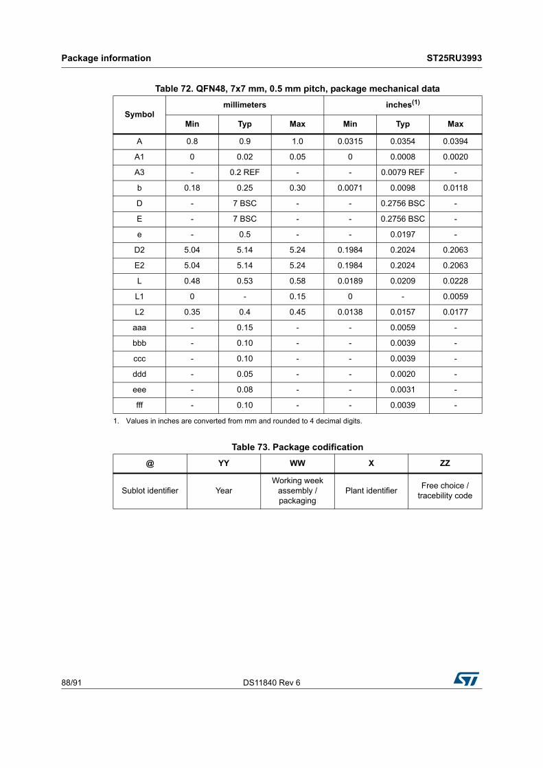
Package information ST25RU3993
88/91 DS11840 Rev 6
Table 72. QFN48, 7x7 mm, 0.5 mm pitch, package mechanical data
Symbolmillimeters inches(1)
1. Values in inches are converted from mm and rounded to 4 decimal digits.
Min Typ Max Min Typ Max
A 0.8 0.9 1.0 0.0315 0.0354 0.0394
A1 0 0.02 0.05 0 0.0008 0.0020
A3 - 0.2 REF - - 0.0079 REF -
b 0.18 0.25 0.30 0.0071 0.0098 0.0118
D - 7 BSC - - 0.2756 BSC -
E - 7 BSC - - 0.2756 BSC -
e - 0.5 - - 0.0197 -
D2 5.04 5.14 5.24 0.1984 0.2024 0.2063
E2 5.04 5.14 5.24 0.1984 0.2024 0.2063
L 0.48 0.53 0.58 0.0189 0.0209 0.0228
L1 0 - 0.15 0 - 0.0059
L2 0.35 0.4 0.45 0.0138 0.0157 0.0177
aaa - 0.15 - - 0.0059 -
bbb - 0.10 - - 0.0039 -
ccc - 0.10 - - 0.0039 -
ddd - 0.05 - - 0.0020 -
eee - 0.08 - - 0.0031 -
fff - 0.10 - - 0.0039 -
Table 73. Package codification
@ YY WW X ZZ
Sublot identifier YearWorking week
assembly / packaging
Plant identifierFree choice /
tracebility code
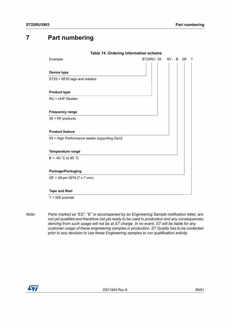
DS11840 Rev 6 89/91
ST25RU3993 Part numbering
90
7 Part numbering
Note: Parts marked as “ES”, “E” or accompanied by an Engineering Sample notification letter, are not yet qualified and therefore not yet ready to be used in production and any consequences deriving from such usage will not be at ST charge. In no event, ST will be liable for any customer usage of these engineering samples in production. ST Quality has to be contacted prior to any decision to use these Engineering samples to run qualification activity.
Table 74. Ordering information scheme
Example: ST25RU 39 93 - B QF T
Device type
ST25 = RFID tags and readers
Product type
RU = UHF Reader
Frequency range
39 = RF products
Product feature
93 = High Performance reader supporting Gen2
Temperature range
B = -40 °C to 85 °C
Package/Packaging
QF = 48-pin QFN (7 x 7 mm)
Tape and Reel
T = 500 pcs/reel
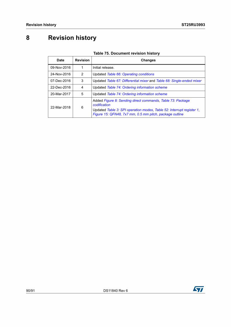
Revision history ST25RU3993
90/91 DS11840 Rev 6
8 Revision history
Table 75. Document revision history
Date Revision Changes
09-Nov-2016 1 Initial release.
24-Nov-2016 2 Updated Table 66: Operating conditions
07-Dec-2016 3 Updated Table 67: Differential mixer and Table 68: Single-ended mixer
22-Dec-2016 4 Updated Table 74: Ordering information scheme
20-Mar-2017 5 Updated Table 74: Ordering information scheme
22-Mar-2018 6
Added Figure 8: Sending direct commands, Table 73: Package codification
Updated Table 3: SPI operation modes, Table 52: Interrupt register 1, Figure 15: QFN48, 7x7 mm, 0.5 mm pitch, package outline

DS11840 Rev 6 91/91
ST25RU3993
91
IMPORTANT NOTICE – PLEASE READ CAREFULLY
STMicroelectronics NV and its subsidiaries (“ST”) reserve the right to make changes, corrections, enhancements, modifications, and improvements to ST products and/or to this document at any time without notice. Purchasers should obtain the latest relevant information on ST products before placing orders. ST products are sold pursuant to ST’s terms and conditions of sale in place at the time of order acknowledgement.
Purchasers are solely responsible for the choice, selection, and use of ST products and ST assumes no liability for application assistance or the design of Purchasers’ products.
No license, express or implied, to any intellectual property right is granted by ST herein.
Resale of ST products with provisions different from the information set forth herein shall void any warranty granted by ST for such product.
ST and the ST logo are trademarks of ST. All other product or service names are the property of their respective owners.
Information in this document supersedes and replaces information previously supplied in any prior versions of this document.
© 2018 STMicroelectronics – All rights reserved


