Ultralow Distortion IF Dual VGA Data Sheet AD8376
Rev. B Document Feedback Information furnished by Analog Devices is believed to be accurate and reliable. However, no responsibility is assumed by Analog Devices for its use, nor for any infringements of patents or other rights of third parties that may result from its use. Specifications subject to change without notice. No license is granted by implication or otherwise under any patent or patent rights of Analog Devices. Trademarks and registered trademarks are the property of their respective owners.
One Technology Way, P.O. Box 9106, Norwood, MA 02062-9106, U.S.A. Tel: 781.329.4700 ©2007–2013 Analog Devices, Inc. All rights reserved. Technical Support www.analog.com
FEATURES Dual independent digitally controlled VGAs Bandwidth of 700 MHz (−3 dB) Gain range: −4 dB to +20 dB Step size: 1 dB ± 0.2 dB Differential input and output Noise figure: 8.7 dB @ maximum gain Output IP3 of ~50 dBm at 200 MHz Output P1dB of 20 dBm at 200 MHz Dual parallel 5-bit control interface Provides constant SFDR vs. gain Power-down control Single 5 V supply operation 32-lead, 5 mm x 5 mm LFCSP
APPLICATIONS Differential ADC drivers Main and diversity IF sampling receivers Wideband multichannel receivers Instrumentation
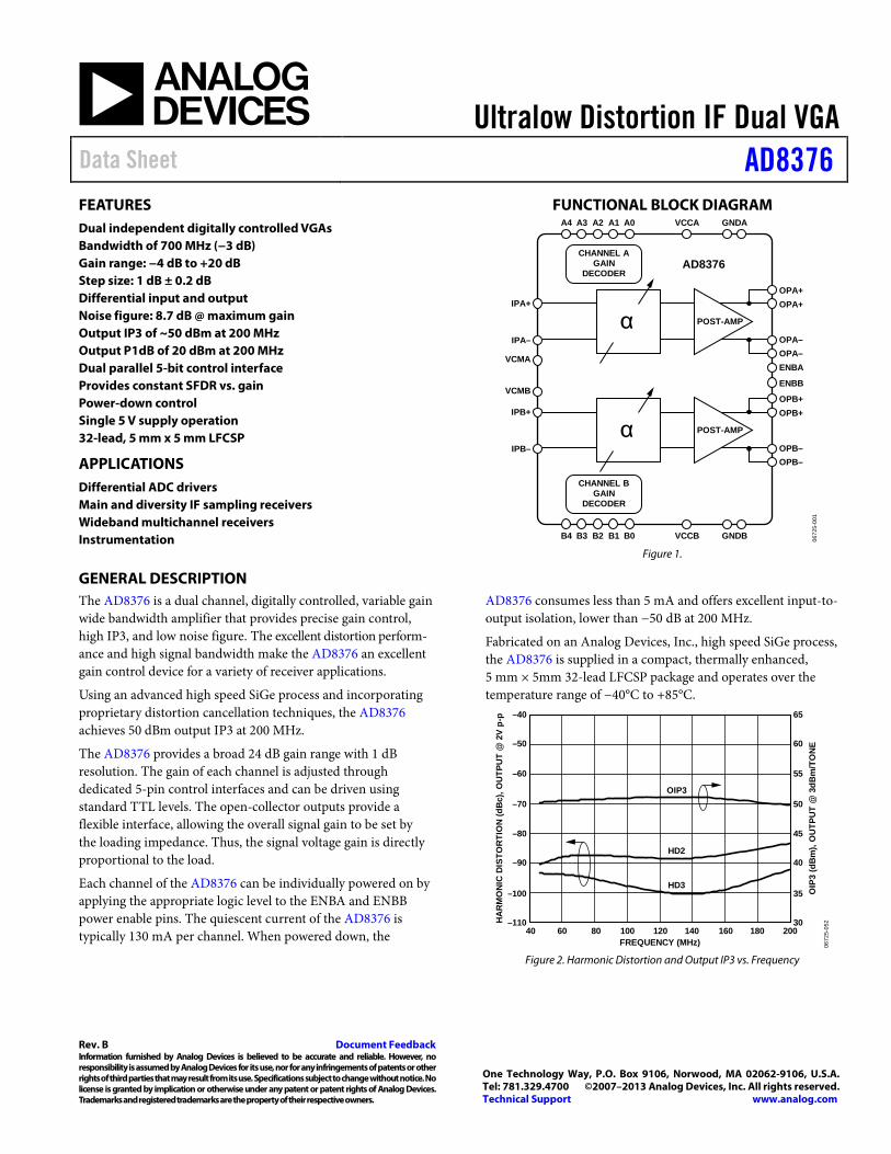
FUNCTIONAL BLOCK DIAGRAM
POST-AMPα
CHANNEL AGAIN
DECODER
CHANNEL BGAIN
DECODER
A0A1A2A3A4
B0B1B2B3B4
GNDAVCCA
GNDBVCCB
AD8376
IPA+
IPA–
VCMA
VCMB
OPA+OPA+
ENBB
OPA–OPA–ENBA
POST-AMPαIPB+
IPB–
OPB+OPB+
OPB–OPB–
0672
5-00
1
Figure 1.
GENERAL DESCRIPTION The AD8376 is a dual channel, digitally controlled, variable gain wide bandwidth amplifier that provides precise gain control, high IP3, and low noise figure. The excellent distortion perform-ance and high signal bandwidth make the AD8376 an excellent gain control device for a variety of receiver applications.
Using an advanced high speed SiGe process and incorporating proprietary distortion cancellation techniques, the AD8376 achieves 50 dBm output IP3 at 200 MHz.
The AD8376 provides a broad 24 dB gain range with 1 dB resolution. The gain of each channel is adjusted through dedicated 5-pin control interfaces and can be driven using standard TTL levels. The open-collector outputs provide a flexible interface, allowing the overall signal gain to be set by the loading impedance. Thus, the signal voltage gain is directly proportional to the load.
Each channel of the AD8376 can be individually powered on by applying the appropriate logic level to the ENBA and ENBB power enable pins. The quiescent current of the AD8376 is typically 130 mA per channel. When powered down, the
AD8376 consumes less than 5 mA and offers excellent input-to-output isolation, lower than −50 dB at 200 MHz.
Fabricated on an Analog Devices, Inc., high speed SiGe process, the AD8376 is supplied in a compact, thermally enhanced, 5 mm × 5mm 32-lead LFCSP package and operates over the temperature range of −40°C to +85°C.
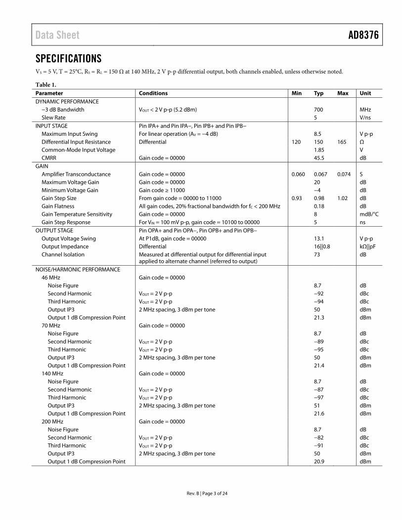
–40
–60
–50
–70
–90
–80
–100
–110
65
55
60
50
40
45
35
30HA
RM
ON
IC D
ISTO
RTI
ON
(dB
c), O
UTP
UT
@ 2
V p-
p
OIP
3 (d
Bm
), O
UTP
UT
@ 3
dBm
/TO
NE
40 60 80 100 120 140 160 180 200FREQUENCY (MHz) 06
725-
052
OIP3
HD2
HD3
Figure 2. Harmonic Distortion and Output IP3 vs. Frequency

AD8376 Data Sheet
Rev. B | Page 2 of 24
TABLE OF CONTENTS Features .............................................................................................. 1 Applications ....................................................................................... 1 Functional Block Diagram .............................................................. 1 General Description ......................................................................... 1 Revision History ............................................................................... 2 Specifications ..................................................................................... 3 Absolute Maximum Ratings ............................................................ 5
ESD Caution .................................................................................. 5 Pin Configuration and Function Descriptions ............................. 6 Typical Performance Characteristics ............................................. 7 Circuit Description ......................................................................... 12
Basic Structure ............................................................................ 12 Applications ..................................................................................... 13
Basic Connections ...................................................................... 13 Single-Ended-to-Differential Conversion ............................... 13 Broadband Operation ................................................................ 15 ADC Interfacing ......................................................................... 15 Layout Considerations ............................................................... 18 Characterization Test Circuits .................................................. 18 Evaluation Board ........................................................................ 19
Outline Dimensions ....................................................................... 23 Ordering Guide .......................................................................... 23
REVISION HISTORY 10/13—Rev. A to Rev. B
Changed ENBA, ENBB, A0 to A4, B0 to B4 Maximum Rating to +0.6 V; Table 3 .............................................................................. 5 Updated Outline Dimensions ....................................................... 23 Changes to Ordering Guide .......................................................... 23
10/10—Rev. 0 to Rev. A
Changes to Figure 3 and Table 4 ..................................................... 6 Changes to Figure 36 ...................................................................... 14 Added Exposed Pad Notation to Outline Dimensions ............. 23
8/07—Revision 0: Initial Version
Data Sheet AD8376
Rev. B | Page 3 of 24
SPECIFICATIONS VS = 5 V, T = 25°C, RS = RL = 150 Ω at 140 MHz, 2 V p-p differential output, both channels enabled, unless otherwise noted.
Table 1. Parameter Conditions Min Typ Max Unit DYNAMIC PERFORMANCE
−3 dB Bandwidth VOUT < 2 V p-p (5.2 dBm) 700 MHz Slew Rate 5 V/ns
INPUT STAGE Pin IPA+ and Pin IPA−, Pin IPB+ and Pin IPB− Maximum Input Swing For linear operation (AV = −4 dB) 8.5 V p-p Differential Input Resistance Differential 120 150 165 Ω Common-Mode Input Voltage 1.85 V CMRR Gain code = 00000 45.5 dB
GAIN Amplifier Transconductance Gain code = 00000 0.060 0.067 0.074 S Maximum Voltage Gain Gain code = 00000 20 dB Minimum Voltage Gain Gain code ≥ 11000 −4 dB Gain Step Size From gain code = 00000 to 11000 0.93 0.98 1.02 dB Gain Flatness All gain codes, 20% fractional bandwidth for fC < 200 MHz 0.18 dB Gain Temperature Sensitivity Gain code = 00000 8 mdB/°C Gain Step Response For VIN = 100 mV p-p, gain code = 10100 to 00000 5 ns
OUTPUT STAGE Pin OPA+ and Pin OPA−, Pin OPB+ and Pin OPB− Output Voltage Swing At P1dB, gain code = 00000 13.1 V p-p Output Impedance Differential 16||0.8 kΩ||pF Channel Isolation Measured at differential output for differential input
applied to alternate channel (referred to output) 73 dB
NOISE/HARMONIC PERFORMANCE 46 MHz Gain code = 00000
Noise Figure 8.7 dB Second Harmonic VOUT = 2 V p-p −92 dBc Third Harmonic VOUT = 2 V p-p −94 dBc Output IP3 2 MHz spacing, 3 dBm per tone 50 dBm Output 1 dB Compression Point 21.3 dBm
70 MHz Gain code = 00000 Noise Figure 8.7 dB Second Harmonic VOUT = 2 V p-p −89 dBc Third Harmonic VOUT = 2 V p-p −95 dBc Output IP3 2 MHz spacing, 3 dBm per tone 50 dBm Output 1 dB Compression Point 21.4 dBm
140 MHz Gain code = 00000 Noise Figure 8.7 dB Second Harmonic VOUT = 2 V p-p −87 dBc Third Harmonic VOUT = 2 V p-p −97 dBc Output IP3 2 MHz spacing, 3 dBm per tone 51 dBm Output 1 dB Compression Point 21.6 dBm
200 MHz Gain code = 00000 Noise Figure 8.7 dB Second Harmonic VOUT = 2 V p-p −82 dBc Third Harmonic VOUT = 2 V p-p −91 dBc Output IP3 2 MHz spacing, 3 dBm per tone 50 dBm Output 1 dB Compression Point 20.9 dBm
AD8376 Data Sheet
Rev. B | Page 4 of 24
Parameter Conditions Min Typ Max Unit POWER INTERFACE
Supply Voltage 4.5 5.0 5.5 V VCC and Output Quiescent Current
with Both Channels Enabled Thermal connection made to exposed paddle under device 245 250 255 mA
vs. Temperature −40°C ≤ TA ≤ +85°C 285 mA Power-Down Current, Both Channels ENBA and ENBB Low 5.4 mA
vs. Temperature −40°C ≤ TA ≤ +85°C 7 mA POWER-UP/GAIN CONTROL Pin A0 to Pin A4, Pin B0 to Pin B4, Pin ENBA, and Pin ENBB
VIH Minimum voltage for a logic high 1.6 V VIL Maximum voltage for a logic low 0.8 V Logic Input Bias Current 900 nA
Table 2. Gain Code vs. Voltage Gain Look-Up Table 5-Bit Binary Gain Code Voltage Gain (dB) 00000 +20 00001 +19 00010 +18 00011 +17 00100 +16 00101 +15 00110 +14 00111 +13 01000 +12 01001 +11 01010 +10 01011 +9 01100 +8
5-Bit Binary Gain Code Voltage Gain (dB) 01101 +7 01110 +6 01111 +5 10000 +4 10001 +3 10010 +2 10011 +1 10100 0 10101 −1 10110 −2 10111 −3 11000 −4 >11000 −4

Data Sheet AD8376
Rev. B | Page 5 of 24
ABSOLUTE MAXIMUM RATINGS Table 3. Parameter Rating Supply Voltage, VPOS 5.5 V ENBA, ENBB, A0 to A4, B0 to B4 −0.6 V to (VPOS + 0.6 V) Input Voltage, VIN+, VIN− −0.15 V to +4.15 V DC Common Mode VCMA, VCMB ± 0.25 V VCMA, VCMB ± 6 mA Internal Power Dissipation 1.6 W θJA (Exposed Paddle Soldered Down) 34.6°C/W θJC (At Exposed Paddle) 3.6°C/W Maximum Junction Temperature 140°C Operating Temperature Range −40°C to +85°C Storage Temperature Range −65°C to +150°C
Stresses above those listed under Absolute Maximum Ratings may cause permanent damage to the device. This is a stress rating only; functional operation of the device at these or any other conditions above those indicated in the operational section of this specification is not implied. Exposure to absolute maximum rating conditions for extended periods may affect device reliability.
ESD CAUTION
AD8376 Data Sheet
Rev. B | Page 6 of 24
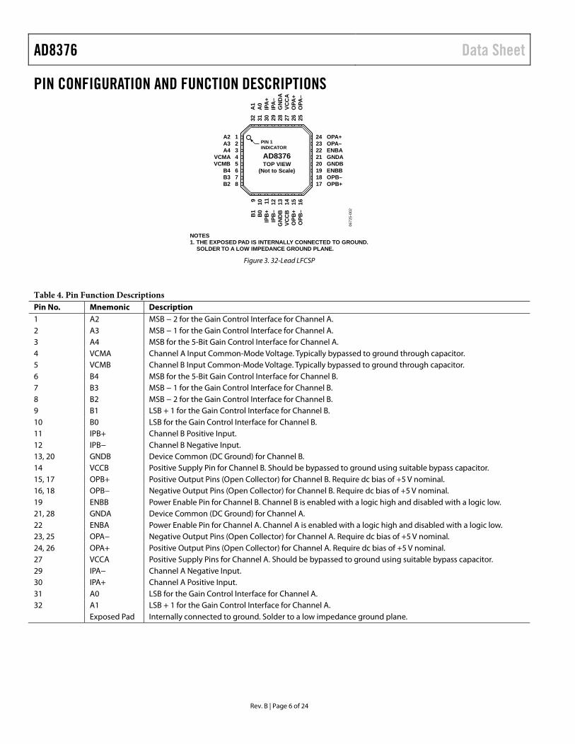
PIN CONFIGURATION AND FUNCTION DESCRIPTIONS
PIN 1INDICATOR
1A22A33A44VCMA
NOTES1. THE EXPOSED PAD IS INTERNALLY CONNECTED TO GROUND. SOLDER TO A LOW IMPEDANCE GROUND PLANE.
5VCMB6B47B38B2
24 OPA+23 OPA–22 ENBA21 GNDA20 GNDB19 ENBB18 OPB–17 OPB+
9B
110
B0
11IP
B+
12IP
B–
13G
ND
B14
VCC
B15
OPB
+16
OPB
–
32A
131
A0
30IP
A+
29IP
A–
28G
ND
A27
VCC
A26
OPA
+25
OPA
–
AD8376TOP VIEW
(Not to Scale)
0672
5-00
2
Figure 3. 32-Lead LFCSP
Table 4. Pin Function Descriptions Pin No. Mnemonic Description 1 A2 MSB − 2 for the Gain Control Interface for Channel A. 2 A3 MSB − 1 for the Gain Control Interface for Channel A. 3 A4 MSB for the 5-Bit Gain Control Interface for Channel A. 4 VCMA Channel A Input Common-Mode Voltage. Typically bypassed to ground through capacitor. 5 VCMB Channel B Input Common-Mode Voltage. Typically bypassed to ground through capacitor. 6 B4 MSB for the 5-Bit Gain Control Interface for Channel B. 7 B3 MSB − 1 for the Gain Control Interface for Channel B. 8 B2 MSB − 2 for the Gain Control Interface for Channel B. 9 B1 LSB + 1 for the Gain Control Interface for Channel B. 10 B0 LSB for the Gain Control Interface for Channel B. 11 IPB+ Channel B Positive Input. 12 IPB− Channel B Negative Input. 13, 20 GNDB Device Common (DC Ground) for Channel B. 14 VCCB Positive Supply Pin for Channel B. Should be bypassed to ground using suitable bypass capacitor. 15, 17 OPB+ Positive Output Pins (Open Collector) for Channel B. Require dc bias of +5 V nominal. 16, 18 OPB− Negative Output Pins (Open Collector) for Channel B. Require dc bias of +5 V nominal. 19 ENBB Power Enable Pin for Channel B. Channel B is enabled with a logic high and disabled with a logic low. 21, 28 GNDA Device Common (DC Ground) for Channel A. 22 ENBA Power Enable Pin for Channel A. Channel A is enabled with a logic high and disabled with a logic low. 23, 25 OPA− Negative Output Pins (Open Collector) for Channel A. Require dc bias of +5 V nominal. 24, 26 OPA+ Positive Output Pins (Open Collector) for Channel A. Require dc bias of +5 V nominal. 27 VCCA Positive Supply Pins for Channel A. Should be bypassed to ground using suitable bypass capacitor. 29 IPA− Channel A Negative Input. 30 IPA+ Channel A Positive Input. 31 A0 LSB for the Gain Control Interface for Channel A. 32 A1 LSB + 1 for the Gain Control Interface for Channel A. Exposed Pad Internally connected to ground. Solder to a low impedance ground plane.
Data Sheet AD8376
Rev. B | Page 7 of 24
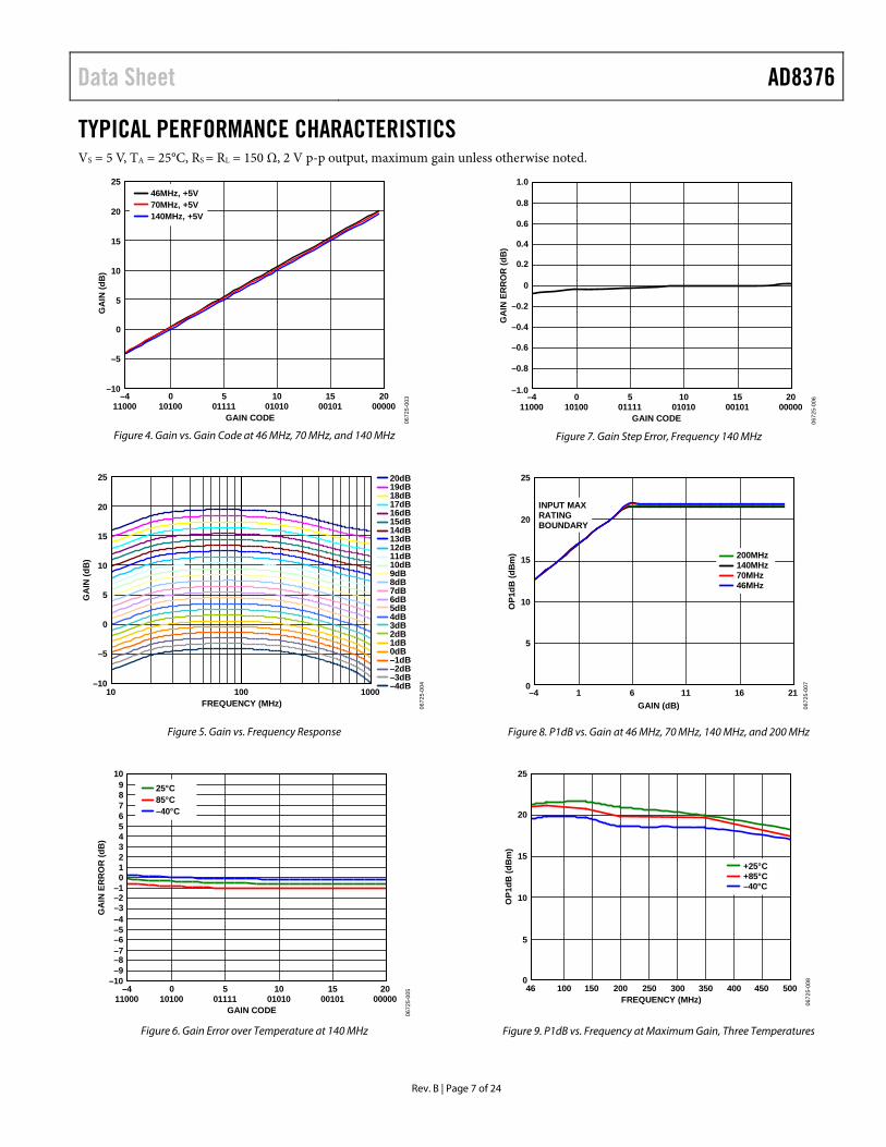
TYPICAL PERFORMANCE CHARACTERISTICS VS = 5 V, TA = 25°C, RS = RL = 150 Ω, 2 V p-p output, maximum gain unless otherwise noted.
25
20
10
15
5
0
–10
–5
GA
IN (d
B)
–411000
010100
501111
1001010
1500101
2000000
GAIN CODE
46MHz, +5V70MHz, +5V140MHz, +5V
0672
5-00
3
Figure 4. Gain vs. Gain Code at 46 MHz, 70 MHz, and 140 MHz
25
20
15
10
5
0
–5
–10
GA
IN (d
B)
10 100 1000FREQUENCY (MHz)
20dB19dB18dB17dB16dB15dB14dB13dB12dB11dB10dB9dB8dB7dB6dB5dB4dB3dB2dB1dB0dB–1dB–2dB–3dB–4dB
0672
5-00
4
Figure 5. Gain vs. Frequency Response
109876543210
–1–2–3–4–5–6–7–8–9
–10
GA
IN E
RR
OR
(dB
)
–411000
010100
501111
1001010
1500101
2000000
GAIN CODE
25°C85°C–40°C
0672
5-00
5
Figure 6. Gain Error over Temperature at 140 MHz
1.0
0.8
0.6
0.4
0.2
0
–0.2
–0.4
–0.6
–0.8
–1.0
GA
IN E
RR
OR
(dB
)
–411000
010100
501111
1001010
1500101
2000000
GAIN CODE 0672
5-00
6
Figure 7. Gain Step Error, Frequency 140 MHz
25
20
15
10
5
0
OP1
dB (d
Bm
)
–4 1 6 11 16 21GAIN (dB) 06
725-
007
INPUT MAXRATINGBOUNDARY
200MHz140MHz70MHz46MHz
Figure 8. P1dB vs. Gain at 46 MHz, 70 MHz, 140 MHz, and 200 MHz
25
20
15
10
5
0
OP1
dB (d
Bm
)
46 100 150 200 250 300 350 400 450 500FREQUENCY (MHz)
+25°C+85°C–40°C
0672
5-00
8
Figure 9. P1dB vs. Frequency at Maximum Gain, Three Temperatures

AD8376 Data Sheet
Rev. B | Page 8 of 24
52
51
50
49
48
47
46
45
44
43
42
4140
30 50 70 90 110 130 150 170 190 210FREQUENCY (MHz)
OIP
3 (d
Bm
)
AV = 0dB
AV = –4dB
AV = +10dB
AV = +20dB
0672
5-00
9
Figure 10. Output Third-Order Intercept at Four Gains, Output Level at 3 dBm/Tone
52
51
50
49
48
47
46
45
44
43
42
4140
–4 –3 –2 –1 0 1 2 3 4 5 6POUT (dBm)
OIP
3 (d
Bm
)
AV = 0dB
AV = –4dB
AV = +20dB
AV = +10dB
0672
5-01
0
Figure 11. Output Third-Order Intercept vs. Power at Four Gains, Frequency 140 MHz
+25°C
+85°C –40°C
70
60
65
55
45
50
40
30
35
OIP
3 (d
Bm
)
40 60 80 100 120 140 160 180 200FREQUENCY (MHz) 06
725-
011
Figure 12. Output Third-Order Intercept vs. Frequency, Three Temperatures, Output Level at 3 dBm/Tone
25
30
35
40
45
50
55
–3 –2 –1 0 1 2 3 4 535
40
45
50
55
60
65
OIP
3 (d
Bm
)
POUT PER TONE (dBm)
OIP
3 (d
Bm
)
+25°C 20dB–40°C 20dB+85°C 20dB+25°C 0dB–40°C 0dB+85°C 0dB
AV = 0dB
AV = 20dB
0672
5-01
2
Figure 13. Output Third-Order Intercept vs. Power, Frequency 140 MHz, Three Temperatures
–70
–80
–75
–85
–95
–90
–100
–110
–105
IMD
3 (d
Bc)
–4 1 6 11 16GAIN (dB) 06
725-
013
46MHz70MHz140MHz200MHz
Figure 14. Two-Tone Output IMD vs. Gain at 46 MHz, 70 MHz, 140 MHz, and 200 MHz, Output Level at 3 dBm/Tone
+25°C
+85°C
–40°C
–70
–80
–75
–85
–95
–90
–100
–110
–105
IMD
3 (d
Bc)
40 60 80 100 120 140 160 180 200FREQUENCY (MHz) 06
725-
014
Figure 15. Two-Tone Output IMD vs. Frequency, Three Temperatures, Output Level at 3 dBm/Tone
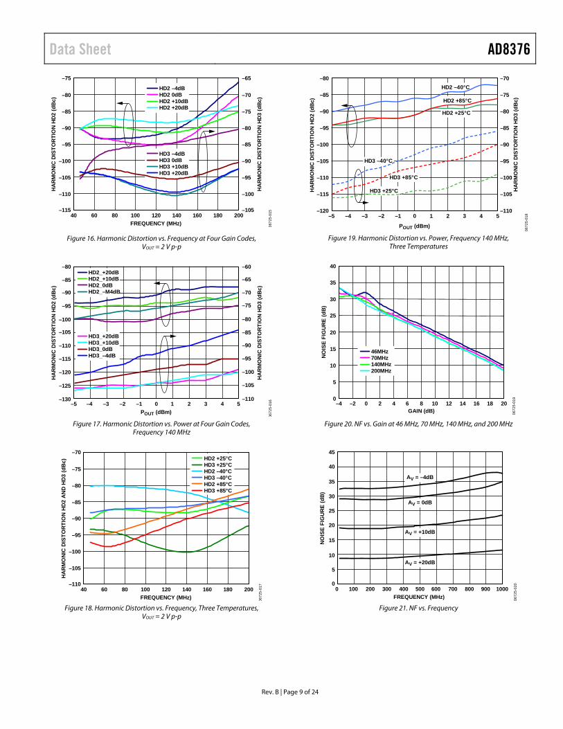
Data Sheet AD8376
Rev. B | Page 9 of 24
–75
–80
–85
–90
–95
–100
–105
–110
–115
–65
–70
–75
–80
–85
–90
–95
–100
–105
HA
RM
ON
IC D
ISTO
RTI
ON
HD
2 (d
Bc)
HA
RM
ON
IC D
ISTO
RTI
ON
HD
3 (d
Bc)
40 60 80 100 120 140 160 180 200FREQUENCY (MHz)
HD2 –4dBHD2 0dBHD2 +10dBHD2 +20dB
HD3 –4dBHD3 0dBHD3 +10dBHD3 +20dB
0672
5-01
5
Figure 16. Harmonic Distortion vs. Frequency at Four Gain Codes, VOUT = 2 V p-p
–80
–85
–90
–95
–100
–105
–110
–115
–120
–125
–130
–60
–65
–70
–75
–80
–85
–90
–95
–100
–105
–110
HA
RM
ON
IC D
ISTO
RTI
ON
HD
2 (d
Bc)
HA
RM
ON
IC D
ISTO
RTI
ON
HD
3 (d
Bc)
–5 –4 –3 –2 –1 0 1 2 3 4 5POUT (dBm)
HD3_+20dBHD3_+10dBHD3_0dBHD3_–4dB
HD2_+20dBHD2_+10dBHD2_0dBHD2_–M4dB
0672
5-01
6
Figure 17. Harmonic Distortion vs. Power at Four Gain Codes, Frequency 140 MHz
–70
–75
–80
–85
–90
–95
–100
–105
–110
HA
RM
ON
IC D
ISTO
RTI
ON
HD
2 A
ND
HD
3 (d
Bc)
40 60 80 100 120 140 160 180 200FREQUENCY (MHz)
HD2 +25°CHD3 +25°CHD2 –40°CHD3 –40°CHD2 +85°CHD3 +85°C
0672
5-01
7
Figure 18. Harmonic Distortion vs. Frequency, Three Temperatures, VOUT = 2 V p-p
–120
–85
–115
–110
–105
–100
–95
–90
–80
–5 –4 –3 –2 –1 0 1 2 3 4 5–110
–105
–100
–95
–90
–85
–80
–75
–70
HA
RM
ON
IC D
ISTO
RTI
ON
HD
3 (d
Bc)
POUT (dBm)
HA
RM
ON
IC D
ISTO
RTI
ON
HD
2 (d
Bc)
HD3 +25°C
HD3 +85°C
HD3 –40°C
HD2 –40°C
HD2 +25°C
HD2 +85°C
0672
5-01
8
Figure 19. Harmonic Distortion vs. Power, Frequency 140 MHz, Three Temperatures
35
40
30
25
20
15
10
5
0
NO
ISE
FIG
UR
E (d
B)
–4 –2 0 2 4 6 8 10 12 14 16 18 20GAIN (dB)
46MHz70MHz140MHz200MHz
0672
5-01
9
Figure 20. NF vs. Gain at 46 MHz, 70 MHz, 140 MHz, and 200 MHz
45
40
35
30
25
20
15
10
5
00 100 200 300 400 500 600 700 800 900 1000
FREQUENCY (MHz)
NO
ISE
FIG
UR
E (d
B)
AV = 0dB
AV = –4dB
AV = +10dB
AV = +20dB
0672
5-02
0
Figure 21. NF vs. Frequency

AD8376 Data Sheet
Rev. B | Page 10 of 24
CH1 500mV Ω CH2 500mV Ω M10.0ns 10.0GS/s IT 10.0ps/ptA CH1 960mV
1
2
0672
5-02
1
Figure 22. Gain Step Time Domain Response
CH1 500mV Ω CH2 500mV Ω M20.0ns 10.0GS/s IT 20.0ps/ptA CH1 960mV
1
2
0672
5-02
2
Figure 23. ENBL Time Domain Response
R4
M2.5ns 20.0GS/s IT 10.0ps/ptA CH4 28.0mV
R3R1
REF1 POSITION–420mV/DIVREF1 SCALE
2V0pF
10pF EACH SIDE
INPUT
REF 1 2.0V 2.5ns 0672
5-02
3
Figure 24. Pulse Response to Capacitive Loading, Gain −4 dB
M2.5ns 20.0GS/s IT 10.0ps/ptA CH4 28.0mV
R3
REF3 POSITION–600mV/DIVREF3 SCALE
500mV0pF
INPUT
R1
10pF EACH SIDE
REF3 500mV 2.5ns 0672
5-02
4
Figure 25. Pulse Response to Capacitive Loading, Gain 20 dB
0672
5-02
5
INPUT
OUTPUT
REF1 50.0mV
REF1
CH2 500mV M2.5ns 20GspsIT 2.5ps/pt
A CH2 –590mV
2
REF1 POSITION –1.08/DIVREF1 SCALE50mVRISE (C2) 1.339nsFALL(C2) 1.367ns
Figure 26. Large Signal Pulse Response
0
–5
–10
–15
–20
–25
–30
180
120
60
0
–60
–120
–18010 100 1000
FREQUENCY (MHz)
S11
MA
G (d
B)
S11
PHA
SE (D
egre
es)
0672
5-02
6
Figure 27. S11 vs. Frequency

Data Sheet AD8376
Rev. B | Page 11 of 24
0
–20
–40
–60
–80
–100
–120
S12
(dB
)
0 100 200 300 400 500 600 700 800 900 1000FREQUENCY (MHz) 06
725-
027
Figure 28. Reverse Isolation vs. Frequency
0
–10
–20
–30
–40
–50
–60
–70
–80
–90
–100
ISO
LATI
ON
(dB
)
10 100 1000FREQUENCY (MHz) 06
725-
028
Figure 29. Off-State Isolation vs. Frequency
1.00E–09
9.00E–10
8.00E–10
7.00E–10
6.00E–10
5.00E–10
4.00E–10
3.00E–10
2.00E–10
1.00E–10
0.00E+00
DEL
AY
(Sec
onds
)
0 100 200 300 400 500 600 700 800 900 1000FREQUENCY (MHz)
0dB, 5V, 25°C+10dB, 5V, 25°C+20dB, 5V, 25°C–4dB, 5V, 25°C
0672
5-02
9
Figure 30. Group Delay vs. Frequency at Gain
–10
–20
–30
–40
–50
–60
–70
–80
–90
ISO
LATI
ON
(dB
)
0 200 400 600 800 900100 300 500 700 1000FREQUENCY (MHz) 06
725-
032
AV = 0dBAV = –4dB
AV = +10dB
AV = +20dB
Figure 31. Channel Isolation (Output to Output) vs. Frequency
60
50
40
30
20
10
0
CM
RR
(dB
)
0 200 400 600 800 900100 300 500 700 1000FREQUENCY (MHz) 06
725-
031
Figure 32. Common-Mode Rejection Ratio vs. Frequency
AD8376 Data Sheet
Rev. B | Page 12 of 24
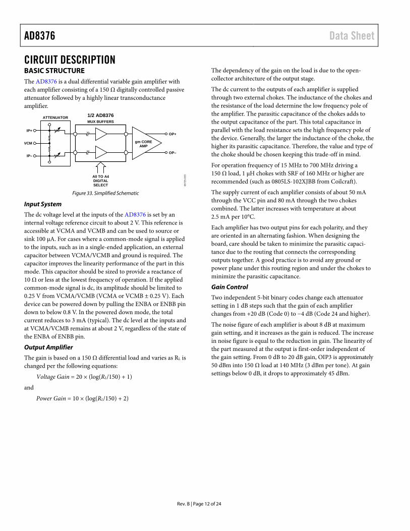
CIRCUIT DESCRIPTION BASIC STRUCTURE The AD8376 is a dual differential variable gain amplifier with each amplifier consisting of a 150 Ω digitally controlled passive attenuator followed by a highly linear transconductance amplifier.
0672
5-03
3
gm COREAMP
MUX BUFFERS1/2 AD8376
A0 TO A4DIGITALSELECT
ATTENUATOR
IP+
VCM
IP–
OP+
OP–
Figure 33. Simplified Schematic
Input System
The dc voltage level at the inputs of the AD8376 is set by an internal voltage reference circuit to about 2 V. This reference is accessible at VCMA and VCMB and can be used to source or sink 100 μA. For cases where a common-mode signal is applied to the inputs, such as in a single-ended application, an external capacitor between VCMA/VCMB and ground is required. The capacitor improves the linearity performance of the part in this mode. This capacitor should be sized to provide a reactance of 10 Ω or less at the lowest frequency of operation. If the applied common-mode signal is dc, its amplitude should be limited to 0.25 V from VCMA/VCMB (VCMA or VCMB ± 0.25 V). Each device can be powered down by pulling the ENBA or ENBB pin down to below 0.8 V. In the powered down mode, the total current reduces to 3 mA (typical). The dc level at the inputs and at VCMA/VCMB remains at about 2 V, regardless of the state of the ENBA of ENBB pin.
Output Amplifier
The gain is based on a 150 Ω differential load and varies as RL is changed per the following equations:
Voltage Gain = 20 × (log(RL/150) + 1)
and
Power Gain = 10 × (log(RL/150) + 2)
The dependency of the gain on the load is due to the open-collector architecture of the output stage.
The dc current to the outputs of each amplifier is supplied through two external chokes. The inductance of the chokes and the resistance of the load determine the low frequency pole of the amplifier. The parasitic capacitance of the chokes adds to the output capacitance of the part. This total capacitance in parallel with the load resistance sets the high frequency pole of the device. Generally, the larger the inductance of the choke, the higher its parasitic capacitance. Therefore, the value and type of the choke should be chosen keeping this trade-off in mind.
For operation frequency of 15 MHz to 700 MHz driving a 150 Ω load, 1 μH chokes with SRF of 160 MHz or higher are recommended (such as 0805LS-102XJBB from Coilcraft).
The supply current of each amplifier consists of about 50 mA through the VCC pin and 80 mA through the two chokes combined. The latter increases with temperature at about 2.5 mA per 10°C.
Each amplifier has two output pins for each polarity, and they are oriented in an alternating fashion. When designing the board, care should be taken to minimize the parasitic capaci-tance due to the routing that connects the corresponding outputs together. A good practice is to avoid any ground or power plane under this routing region and under the chokes to minimize the parasitic capacitance.
Gain Control
Two independent 5-bit binary codes change each attenuator setting in 1 dB steps such that the gain of each amplifier changes from +20 dB (Code 0) to −4 dB (Code 24 and higher).
The noise figure of each amplifier is about 8 dB at maximum gain setting, and it increases as the gain is reduced. The increase in noise figure is equal to the reduction in gain. The linearity of the part measured at the output is first-order independent of the gain setting. From 0 dB to 20 dB gain, OIP3 is approximately 50 dBm into 150 Ω load at 140 MHz (3 dBm per tone). At gain settings below 0 dB, it drops to approximately 45 dBm.

Data Sheet AD8376
Rev. B | Page 13 of 24
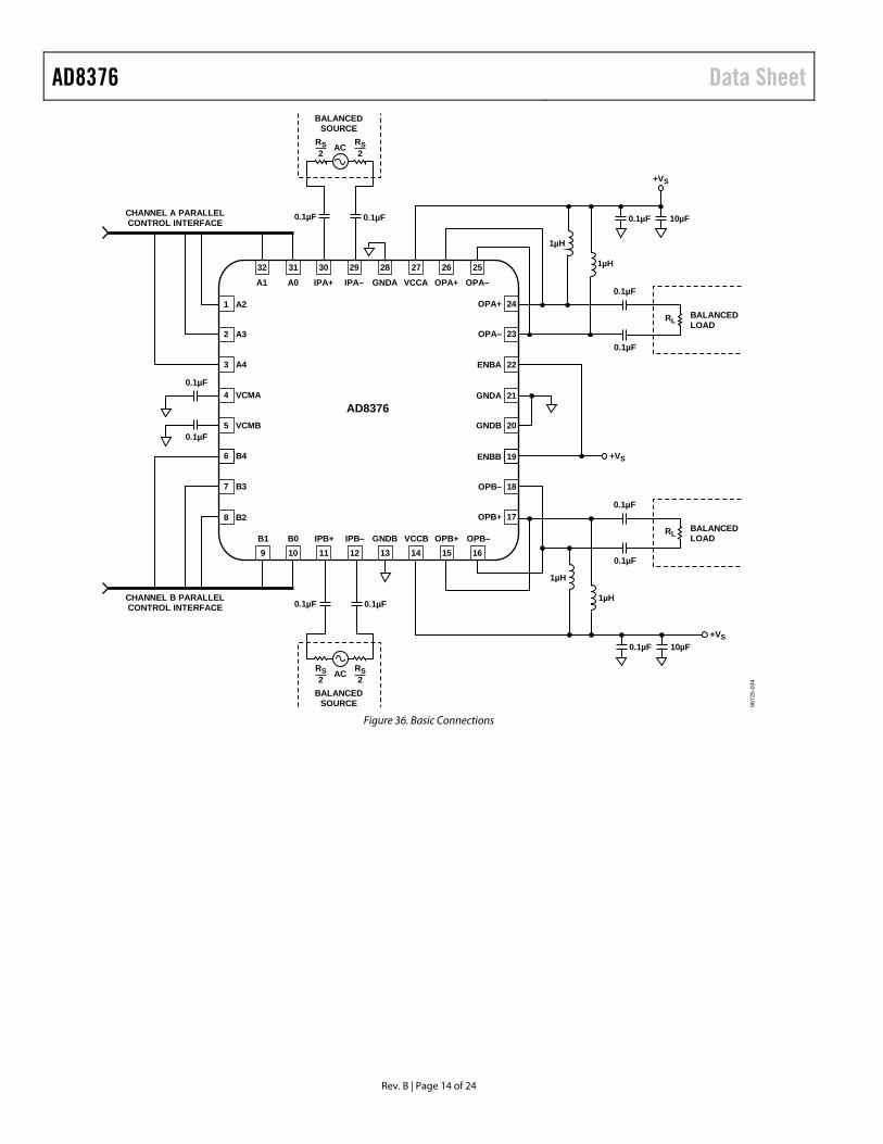
APPLICATIONS BASIC CONNECTIONS Figure 36 shows the basic connections for operating the AD8376. A voltage between 4.5 V and 5.5 V should be applied to the supply pins. Each supply pin should be decoupled with at least one low inductance, surface-mount ceramic capacitor of 0.1 μF placed as close as possible to the device.
The outputs of the AD8376 are open collectors that need to be pulled up to the positive supply with 1 µH RF chokes. The differ-ential outputs are biased to the positive supply and require ac-coupling capacitors, preferably 0.1 µF. Similarly, the input pins are at bias voltages of about 2 V above ground and should be ac-coupled as well. The ac-coupling capacitors and the RF chokes are the principle limitations for operation at low frequencies.
To enable each channel of the AD8376, the ENBA or ENBB pin must be pulled high. Taking ENBA or ENBB low puts the channels of the AD8376 in sleep mode, reducing current consumption to approximately 5 mA per channel at ambient.
SINGLE-ENDED-TO-DIFFERENTIAL CONVERSION The AD8376 can be configured as a single-ended input to differential output driver, as shown in Figure 34. A 150 Ω resistor in parallel with the input impedance of input pin provides an impedance matching of 50 Ω. The voltage gain and the bandwidth of this configuration, using a 150 Ω load, remains the same as when using a differential input.
Using a single-ended input decreases the power gain by 3 dB and limits distortion cancellation. Consequently, the second-order distortion is degraded. The third-order distortion remains low to 200 MHz, as shown in Figure 35.
5
0.1µF
0.1µF
0.1µF
0.1µF
37.5Ω
150Ω
1/2AD8376
1µH
150Ω
A0 TO A4
1µH
+5V
0672
5-03
5
VCM
0.1µF
50Ω
AC
Figure 34. Single-Ended-to-Differential Conversion
Featuring ½ of the AD8376
0672
5-03
6
–60
–65
–70
–75
–80
–85
–90
–95
–100
HA
RM
ON
IC D
ISTO
RTI
ON
(dB
c)
0 20015010050FREQUENCY (MHz)
HD2
HD3
Figure 35. Harmonic Distortion vs. Frequency of
Single-Ended-to-Differential Conversion
AD8376 Data Sheet
Rev. B | Page 14 of 24
0672
5-03
4
0.1µF
0.1µF
0.1µF 0.1µF
0.1µF
0.1µF
1µH
1µH
IPA+ IPA– GNDA VCCA OPA+ OPA–
2530 29 28
A1 A0
32 31 27 26
IPB+ IPB– GNDB VCCB OPB+ OPB–1611 12 13
B1 B09 10 14 15
24
23
22
21
20
19
1
2
3
4
5
6
A2
A3
A4
VCMA
VCMB
B4
7
8
B3
B2
OPA+
OPA–
ENBA
GNDA
GNDB
ENBB
18
17
OPB–
OPB+
AD8376
ACRS2
RS2
BALANCEDSOURCE
0.1µF 0.1µF
ACRS2
RS2
BALANCEDSOURCE
CHANNEL A PARALLELCONTROL INTERFACE
CHANNEL B PARALLELCONTROL INTERFACE
RLBALANCEDLOAD
0.1µF 10µF
0.1µF 10µF
+VS
+VS
0.1µF
0.1µF
RLBALANCEDLOAD
+VS
1µH
1µH
Figure 36. Basic Connections
Data Sheet AD8376
Rev. B | Page 15 of 24
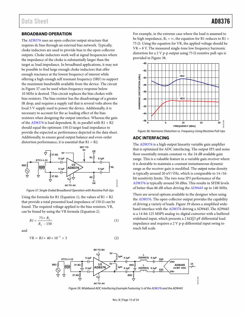
BROADBAND OPERATION The AD8376 uses an open-collector output structure that requires dc bias through an external bias network. Typically, choke inductors are used to provide bias to the open-collector outputs. Choke inductors work well at signal frequencies where the impedance of the choke is substantially larger than the target ac load impedance. In broadband applications, it may not be possible to find large enough choke inductors that offer enough reactance at the lowest frequency of interest while offering a high enough self resonant frequency (SRF) to support the maximum bandwidth available from the device. The circuit in Figure 37 can be used when frequency response below 10 MHz is desired. This circuit replaces the bias chokes with bias resistors. The bias resistor has the disadvantage of a greater IR drop, and requires a supply rail that is several volts above the local 5 V supply used to power the device. Additionally, it is necessary to account for the ac loading effect of the bias resistors when designing the output interface. Whereas the gain of the AD8376 is load dependent, RL in parallel with R1 + R2 should equal the optimum 150 Ω target load impedance to provide the expected ac performance depicted in the data sheet. Additionally, to ensure good output balance and even-order distortion performance, it is essential that R1 = R2.
5
0.1µF
0.1µF
0.1µF
0.1µF50Ω
ETC1-1-13
37.5Ω
37.5Ω5V
SET TO5V
R1
R2
VR
VR
RL
A0 TO A4
1/2AD8376
0672
5-03
7
Figure 37. Single-Ended Broadband Operation with Resistive Pull-Ups
Using the formula for R1 (Equation 1), the values of R1 = R2 that provide a total presented load impedance of 150 Ω can be found. The required voltage applied to the bias resistors, VR, can be found by using the VR formula (Equation 2).
15075
−
×=
L
L
RR
R1 (1)
and
51040 3 +××= −R1VR (2)
For example, in the extreme case where the load is assumed to be high impedance, RL = ∞, the equation for R1 reduces to R1 = 75 Ω. Using the equation for VR, the applied voltage should be VR = 8 V. The measured single-tone low frequency harmonic distortion for a 2 V p-p output using 75 Ω resistive pull-ups is provided in Figure 38.
–80
–82
–84
–86
–88
–90
–92
–94
–96
HA
RM
ON
IC D
ISTO
RTI
ON
(dB
c)
0 5 10 15 20FREQUENCY (MHz)
HD2
HD3
0672
5-03
8
Figure 38. Harmonic Distortion vs. Frequency Using Resistive Pull-Ups
ADC INTERFACING The AD8376 is a high output linearity variable gain amplifier that is optimized for ADC interfacing. The output IP3 and noise floor essentially remain constant vs. the 24 dB available gain range. This is a valuable feature in a variable gain receiver where it is desirable to maintain a constant instantaneous dynamic range as the receiver gain is modified. The output noise density is typically around 20 nV/√Hz, which is comparable to 14-/16-bit sensitivity limits. The two-tone IP3 performance of the AD8376 is typically around 50 dBm. This results in SFDR levels of better than 86 dB when driving the AD9445 up to 140 MHz.
There are several options available to the designer when using the AD8376. The open-collector output provides the capability of driving a variety of loads. Figure 39 shows a simplified wide-band interface with the AD8376 driving a AD9445. The AD9445 is a 14-bit 125 MSPS analog-to-digital converter with a buffered wideband input, which presents a 2 kΩ||3 pF differential load impedance and requires a 2 V p-p differential input swing to reach full scale.
0.1µF
0.1µF50Ω
ETC1-1-13
37.5Ω
37.5Ω
0.1µF
0.1µF
0.1µF
0.1µF82Ω
82Ω
1µH5V
1µH5V
33Ω
33Ω
14AD944514-BIT ADC
1/2AD8376
5
5
B0 TO B4
A0 TO A4 0672
5-03
9
L(SERIES)
L(SERIES)
VIN+
VIN–
Figure 39. Wideband ADC Interfacing Example Featuring ½ of the AD8376 and the AD9445

AD8376 Data Sheet
Rev. B | Page 16 of 24
For optimum performance, the AD8376 should be driven differentially using an input balun or impedance transformer. Figure 39 uses a wideband 1:1 transmission line balun followed by two 37.5 Ω resistors in parallel with the 150 Ω input imped-ance of the AD8376 to provide a 50 Ω differential terminated input impedance. This provides a wideband match to a 50 Ω source. The open-collector outputs of the AD8376 are biased through the two 1 μH inductors and are ac-coupled to the two 82 Ω load resistors. The 82 Ω load resistors in parallel with the series-terminated ADC impedance yields the target 150 Ω differential load impedance, which is recommended to provide the specified gain accuracy of the device. The load resistors are ac-coupled from the AD9445 to avoid common-mode dc loading. The 33 Ω series resistors help to improve the isolation between the AD8376 and any switching currents present at the analog-to-digital sample and hold input circuitry.
0–10–20–30–40–50–60–70–80–90
–100–110–120–130–140–150
(dB
FS)
0 5.25 10.50 15.75 21.00 26.25 31.50 36.75 42.00 47.25 52.50FREQUENCY (MHz)
SNR = 64.93dBcSFDR = 86.37dBcNOISE FLOOR = –108.1dBFUND = –1.053dBFsSECOND = –86.18dBcTHIRD = –86.22dBc
1
2 3
4 5 6+
0672
5-04
0
Figure 40. Measured Single-Tone Performance of the
Circuit in Figure 39 for a 100 MHz Input Signal
The circuit depicted in Figure 39 provides variable gain, isolation, and source matching for the AD9445. Using this circuit with the AD8376 in a gain of 20 dB (maximum gain), an SFDR performance of 86 dBc is achieved at 100 MHz, as indicated in Figure 40.
The addition of the series inductors L (series) in Figure 39 extends the bandwidth of the system and provides response flatness. Using 100 nH inductors as L (series), the wideband system response of Figure 41 is obtained. The wideband frequency response is an advantage in broadband applications such as predistortion receiver designs and instrumentation applications. However, by designing for a wide analog input frequency range, the cascaded SNR performance is somewhat degraded due to high frequency noise aliasing into the wanted Nyquist zone.
0
–1
–2
–3
–4
–5
–6
–7
–8
–9
–10
(dB
FS)
20 48 76 104 132 160 188 216 244 272 300FREQUENCY (MHz)
FIRST POINT = –2.93dBFsEND POINT = –9.66dBFsMID POINT = –2.33dBFsMIN = –9.66dBFsMAX = –1.91dBFs
0672
5-04
1
Figure 41. Measured Frequency Response of Wideband
ADC Interface Depicted in Figure 39
An alternative narrow-band approach is presented in Figure 42. By designing a narrow band-pass antialiasing filter between the AD8376 and the target ADC, the output noise of the AD8376 outside of the intended Nyquist zone can be attenuated, helping to preserve the available SNR of the ADC. In general, the SNR improves several dB when including a reasonable order antialias-ing filter. In this example, a low loss 1:3 input transformer is used to match the AD8376’s 150 Ω balanced input to a 50 Ω unbal-anced source, resulting in minimum insertion loss at the input.
Data Sheet AD8376
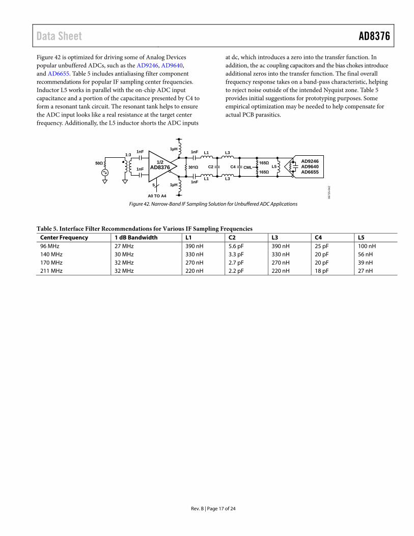
Rev. B | Page 17 of 24
Figure 42 is optimized for driving some of Analog Devices popular unbuffered ADCs, such as the AD9246, AD9640, and AD6655. Table 5 includes antialiasing filter component recommendations for popular IF sampling center frequencies. Inductor L5 works in parallel with the on-chip ADC input capacitance and a portion of the capacitance presented by C4 to form a resonant tank circuit. The resonant tank helps to ensure the ADC input looks like a real resistance at the target center frequency. Additionally, the L5 inductor shorts the ADC inputs
at dc, which introduces a zero into the transfer function. In addition, the ac coupling capacitors and the bias chokes introduce additional zeros into the transfer function. The final overall frequency response takes on a band-pass characteristic, helping to reject noise outside of the intended Nyquist zone. Table 5 provides initial suggestions for prototyping purposes. Some empirical optimization may be needed to help compensate for actual PCB parasitics.
5
1nF
1nF
1nF
1nF
50Ω
1:3
1/2AD8376 301Ω C2
A0 TO A4
C4
1µH
1µH
L1
L1
L3
L3
CML165Ω
165ΩL5
AD9246AD9640AD6655
0672
5-04
2
Figure 42. Narrow-Band IF Sampling Solution for Unbuffered ADC Applications
Table 5. Interface Filter Recommendations for Various IF Sampling Frequencies Center Frequency 1 dB Bandwidth L1 C2 L3 C4 L5 96 MHz 27 MHz 390 nH 5.6 pF 390 nH 25 pF 100 nH 140 MHz 30 MHz 330 nH 3.3 pF 330 nH 20 pF 56 nH 170 MHz 32 MHz 270 nH 2.7 pF 270 nH 20 pF 39 nH 211 MHz 32 MHz 220 nH 2.2 pF 220 nH 18 pF 27 nH
AD8376 Data Sheet
Rev. B | Page 18 of 24
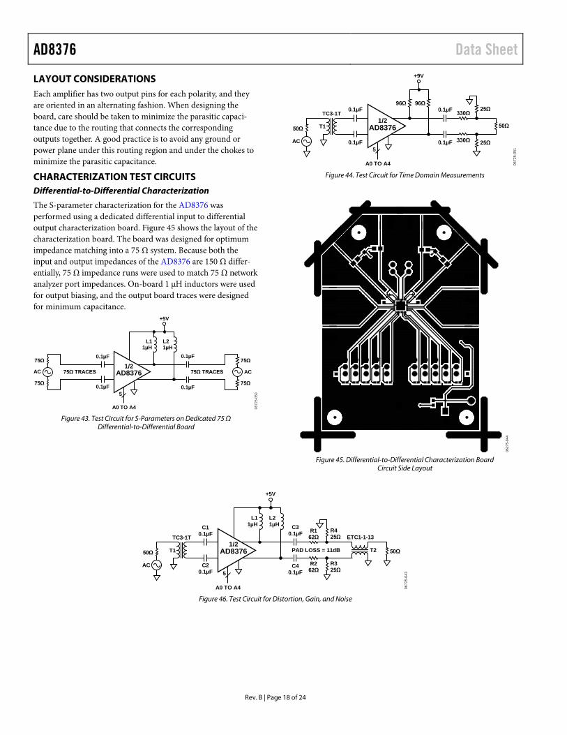
LAYOUT CONSIDERATIONS Each amplifier has two output pins for each polarity, and they are oriented in an alternating fashion. When designing the board, care should be taken to minimize the parasitic capaci-tance due to the routing that connects the corresponding outputs together. A good practice is to avoid any ground or power plane under this routing region and under the chokes to minimize the parasitic capacitance.
CHARACTERIZATION TEST CIRCUITS Differential-to-Differential Characterization
The S-parameter characterization for the AD8376 was performed using a dedicated differential input to differential output characterization board. Figure 45 shows the layout of the characterization board. The board was designed for optimum impedance matching into a 75 Ω system. Because both the input and output impedances of the AD8376 are 150 Ω differ-entially, 75 Ω impedance runs were used to match 75 Ω network analyzer port impedances. On-board 1 μH inductors were used for output biasing, and the output board traces were designed for minimum capacitance.
0.1µF
0.1µF
0672
5-05
0
L11µH
L21µH
0.1µF
0.1µF
+5V
5
A0 TO A4
AC 75Ω TRACES75Ω TRACES
75Ω
75Ω
75Ω
75Ω
AC1/2
AD8376
Figure 43. Test Circuit for S-Parameters on Dedicated 75 Ω
Differential-to-Differential Board
0.1µF
0.1µF
TC3-1T
0672
5-05
1
T1
0.1µF
0.1µF
330Ω
330Ω
25Ω
25Ω
50Ω
+9V
5
A0 TO A4
50Ω
96Ω 96Ω
AC
1/2AD8376
Figure 44. Test Circuit for Time Domain Measurements
0627
5-04
4
Figure 45. Differential-to-Differential Characterization Board
Circuit Side Layout
C10.1µF
C20.1µF
TC3-1T
0672
5-04
3
T1
L11µH
L21µH C3
0.1µF
C40.1µF
R162Ω
R262Ω
R425Ω
R325Ω
ETC1-1-13
T2 50ΩPAD LOSS = 11dB
+5V
5
A0 TO A4
50Ω
AC
1/2AD8376
Figure 46. Test Circuit for Distortion, Gain, and Noise

Data Sheet AD8376
Rev. B | Page 19 of 24
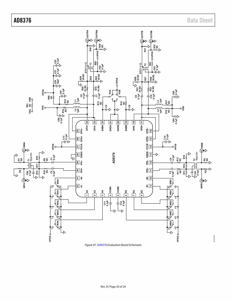
EVALUATION BOARD Figure 47 shows the schematic of the AD8376 evaluation board. The silkscreen and layout of the component and circuit sides are shown in Figure 48 through Figure 51. The board is powered by a single supply in the 4. 5 V to 5.5 V range. The power supply is decoupled by 10 µF and 0.1 µF capacitors at each power supply pin. Additional decoupling, in the form of a series resistor or inductor at the supply pins, can also be added. Table 6 details the various configuration options of the evaluation board.
The output pins of the AD8376 require supply biasing with 1 µH RF chokes. Both the input and output pins must be ac-coupled. These pins are converted to single-ended with a pair of baluns (Mini-Circuits® TC3-1T+ and M/A-COM ETC1-1-13). The baluns at the input, T1 and T2, are used to transform 50 Ω source impedances to the desired 150 Ω reference levels. The output baluns, T3 and T4, and the matching components are configured to provide 150 Ω to 50 Ω impedance transformations with insertion losses of about 11 dB.
AD8376 Data Sheet
Rev. B | Page 20 of 24
R2630.9Ω
R27
R2830.9Ω
T4
C9
0.1µF
C10
0.1µF
R21
61.9Ω
R22
61.9Ω
L4
1µH
L31µH
C64
0.1µF
C650.1µF
R170Ω
R18 0Ω
VPOS
R63
C630.1µF
ETC1-1-13
R320Ω
R31
OUTPB
OUTNB
VXB
VPOS
R13 0Ω R14 0Ω
PUA
PUB
C5
C6
WB0
WB1
WB2
WB3
WB4
VPOS
0 1
0 1
0 1
0 1
0 1R11 0Ω
R73
R74
R75
R120Ω T2C40.1µF
C3
0.1µF
C61
0.1µF
R40ΩTC3-1T+
R3
INPB
INNB
C140.1µF
VPOS
C11
0.1µF
C12
0.1µF
WA0
WA1
WA2
WA3
WA4
VPOS
01
01
01
01
01
C130.1µF
VPOS
R2
R72
R71
R70
R10Ω
C60
0.1µF
T1TC3-1T+
INNA
INPA
R90Ω
R10 0Ω C2
0.1µF
C10.1µF
R2530.9Ω
R24
R2330.9Ω
T3
C8
0.1µF
C7
0.1µF
R20
61.9Ω
R90 0Ω
R19
61.9Ω
L2
1µH
L11µH
C66
0.1µF
C670.1µF
R150Ω
R16 0Ω
VPOS
VPOS
R62
C620.1µF
ETC1-1-13
R290Ω
R30
OUTPA
OUTNA
VXA
C210.1µF
C2010µF
C220.1µF
IPA+
IPA–
GNDAVCCAOPA+OPA–
2530
2928
A1
A0
3231
2726
IPB+
IPB–GNDBVCCBOPB+
OPB–
1611
1213
B1
B0
910
1415
24 23 22 21 20 19
1 2 3 4 5 6
A2
A3
A4
VCMA
VCMB
B4
7 8
B3
B2
OPA+
OPA–
ENBA
GNDA
GNDB
ENBB
18 17
OPB–
OPB+
AD8376
VXB
VXA
R91 0Ω
0672
5-04
5
Figure 47. AD8376 Evaluation Board Schematic
Data Sheet AD8376
Rev. B | Page 21 of 24
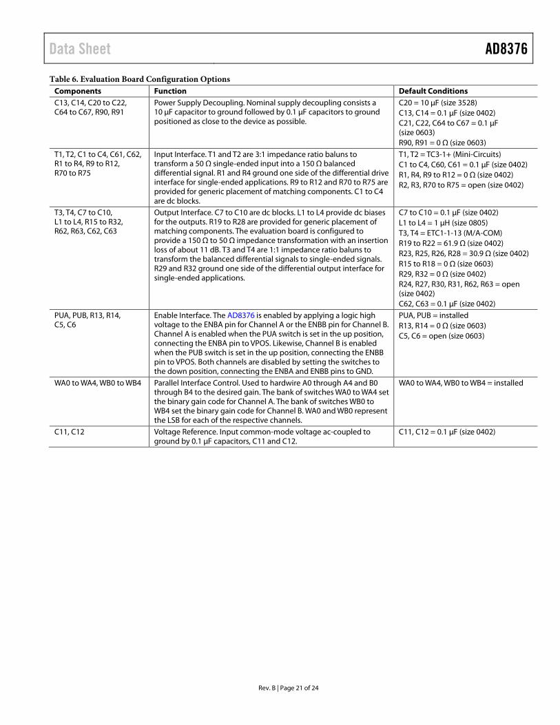
Table 6. Evaluation Board Configuration Options Components Function Default Conditions C13, C14, C20 to C22, C64 to C67, R90, R91
Power Supply Decoupling. Nominal supply decoupling consists a 10 µF capacitor to ground followed by 0.1 µF capacitors to ground positioned as close to the device as possible.
C20 = 10 µF (size 3528) C13, C14 = 0.1 µF (size 0402) C21, C22, C64 to C67 = 0.1 µF (size 0603) R90, R91 = 0 Ω (size 0603)
T1, T2, C1 to C4, C61, C62, R1 to R4, R9 to R12, R70 to R75
Input Interface. T1 and T2 are 3:1 impedance ratio baluns to transform a 50 Ω single-ended input into a 150 Ω balanced differential signal. R1 and R4 ground one side of the differential drive interface for single-ended applications. R9 to R12 and R70 to R75 are provided for generic placement of matching components. C1 to C4 are dc blocks.
T1, T2 = TC3-1+ (Mini-Circuits) C1 to C4, C60, C61 = 0.1 µF (size 0402) R1, R4, R9 to R12 = 0 Ω (size 0402) R2, R3, R70 to R75 = open (size 0402)
T3, T4, C7 to C10, L1 to L4, R15 to R32, R62, R63, C62, C63
Output Interface. C7 to C10 are dc blocks. L1 to L4 provide dc biases for the outputs. R19 to R28 are provided for generic placement of matching components. The evaluation board is configured to provide a 150 Ω to 50 Ω impedance transformation with an insertion loss of about 11 dB. T3 and T4 are 1:1 impedance ratio baluns to transform the balanced differential signals to single-ended signals. R29 and R32 ground one side of the differential output interface for single-ended applications.
C7 to C10 = 0.1 µF (size 0402) L1 to L4 = 1 µH (size 0805) T3, T4 = ETC1-1-13 (M/A-COM) R19 to R22 = 61.9 Ω (size 0402) R23, R25, R26, R28 = 30.9 Ω (size 0402) R15 to R18 = 0 Ω (size 0603) R29, R32 = 0 Ω (size 0402) R24, R27, R30, R31, R62, R63 = open (size 0402) C62, C63 = 0.1 µF (size 0402)
PUA, PUB, R13, R14, C5, C6
Enable Interface. The AD8376 is enabled by applying a logic high voltage to the ENBA pin for Channel A or the ENBB pin for Channel B. Channel A is enabled when the PUA switch is set in the up position, connecting the ENBA pin to VPOS. Likewise, Channel B is enabled when the PUB switch is set in the up position, connecting the ENBB pin to VPOS. Both channels are disabled by setting the switches to the down position, connecting the ENBA and ENBB pins to GND.
PUA, PUB = installed R13, R14 = 0 Ω (size 0603) C5, C6 = open (size 0603)
WA0 to WA4, WB0 to WB4 Parallel Interface Control. Used to hardwire A0 through A4 and B0 through B4 to the desired gain. The bank of switches WA0 to WA4 set the binary gain code for Channel A. The bank of switches WB0 to WB4 set the binary gain code for Channel B. WA0 and WB0 represent the LSB for each of the respective channels.
WA0 to WA4, WB0 to WB4 = installed
C11, C12 Voltage Reference. Input common-mode voltage ac-coupled to ground by 0.1 µF capacitors, C11 and C12.
C11, C12 = 0.1 µF (size 0402)

AD8376 Data Sheet
Rev. B | Page 22 of 24
\ 0672
5-04
6
Figure 48. Component Side Silkscreen
0672
5-04
7
Figure 49. Circuit Side Silkscreen
0672
5-04
8
Figure 50. Component Side Layout
0672
5-04
9
Figure 51. Circuit Side Layout
Data Sheet AD8376
Rev. B | Page 23 of 24
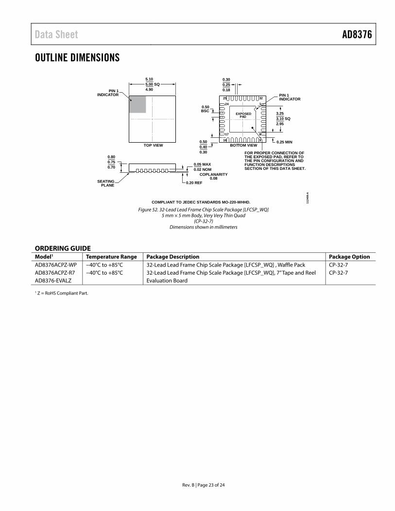
OUTLINE DIMENSIONS
COMPLIANT TO JEDEC STANDARDS MO-220-WHHD. 1124
08-A
10.50BSC
BOTTOM VIEWTOP VIEW
PIN 1INDICATOR
32
916
17
24
25
8
EXPOSEDPAD
PIN 1INDICATOR
3.253.10 SQ2.95
SEATINGPLANE
0.05 MAX0.02 NOM
0.20 REF
COPLANARITY0.08
0.300.250.18
5.105.00 SQ4.90
0.800.750.70
FOR PROPER CONNECTION OFTHE EXPOSED PAD, REFER TOTHE PIN CONFIGURATION ANDFUNCTION DESCRIPTIONSSECTION OF THIS DATA SHEET.
0.500.400.30
0.25 MIN
Figure 52. 32-Lead Lead Frame Chip Scale Package [LFCSP_WQ]
5 mm × 5 mm Body, Very Very Thin Quad (CP-32-7)
Dimensions shown in millimeters
ORDERING GUIDE Model1 Temperature Range Package Description Package Option AD8376ACPZ-WP −40°C to +85°C 32-Lead Lead Frame Chip Scale Package [LFCSP_WQ] , Waffle Pack CP-32-7 AD8376ACPZ-R7 −40°C to +85°C 32-Lead Lead Frame Chip Scale Package [LFCSP_WQ], 7” Tape and Reel CP-32-7 AD8376-EVALZ Evaluation Board 1 Z = RoHS Compliant Part.

AD8376 Data Sheet
Rev. B | Page 24 of 24
NOTES
©2007–2013 Analog Devices, Inc. All rights reserved. Trademarks and registered trademarks are the property of their respective owners. D06725-0-10/13(B)


