UNIVERSITI PUTRA MALAYSIA
PREPARATION OF TIN SELENIDE THIN FILM SEMICONDUCTOR BY ELECTROCHEMICAL DEPOSITION AND ELECTROSELENISATION
ALI JIMALE ALI
FSAS 2000 10
PREPARATION OF TIN SELENIDE THIN FILM SEMICONDUCTOR BY ELECTROCHEMICAL DEPOSITION AND ELECTROSELENISATION
By
ALI J1MALE ALI
Thesis Submitted in Fulfilment of the Requirements for the Degree of Master of Science in the Faculty of
Science and Environmental Studies Universiti Putra Malaysia
September 2000

II
Abstract of thesis presented to the Senate of Universiti Putra Malaysia in fulfilment of the requirements for the degree of Master of Science
PREPARATION OF TIN SELENIDE THIN FILM SEMICONDUCTOR BY ELECTROCHEMICAL DEPOSITION AND ELECTROSELENISATION
By
ALI JIMALE ALI
September 2000
Chairman: Associate Professor Zulkarnain Zainal, Ph.D.
Faculty: Science and Environmental Studies
Electrochemical preparation of tin selenide thin film semiconductor for
photoe1ectrochemical cells (PECs) was studied. The film has been potentiostatically
deposited on tin substrate at room temperature from aqueous solution containing
SnCh and Na2Se03. The effect of the electrodeposition potentials and bath
electrolytes concentrations proportion were investigated to detennine the optimum
condition for electrodeposition. The structure, morphology and the photosensitivity
of the electrosynthesised samples were studied by using X-ray diffiaction, scanning
electron microscopy (SEM) and linear sweep voltammetry techniques. The bandgap
energy and type of optical transition were detennined from optical absorbance data.
The X-ray diffraction analysis confirmed the formation of polycrystalline SnSe on
the tin substrate. Scanning electron microscopy reaffirmed the existence of a
crystalline deposit with different grain size and shape. The films prepared in this
study showed a p-type semiconductor behaviour with very good photosensitivity. The

III
optical absorbance is in the visible light range and the bandgap energy (Eg) is ].0 eV.
The tin selenide thin film semiconductor was also deposited alternately, through
electroselenisation technique on ITO-glass, from aqueous SnCb and Na2Se03
solutions in separate baths. The film showed very good photosensitivity, a p-type
semiconductor behaviour and energy gap of 0.95 eV, but the XRD analysis cannot
confirm the existence of tin selenide due to the very thin layer of the deposit.

Abstrak tesis yang dikemukakan kepada Senat Universiti Putra Malaysia sebagai memenuhi keperluan untuk ijazah Master Sains
IV
PENYEDIAAN LAPISAN NIPIS SEMIKONDUKTOR TIMAH SULFIDA
MELALUI PENGENAPAN ELEKTROKIMIA DAN ELEKTROSELENISASI
Oleh
ALI JIMALE ALI
September 2000
Pengerusi: Profesor Madya Zulkarnain Zainal, Ph.D.
Fakulti: Sains dan Pengajian Alam Sekitar
Penyediaan filem nipis semikonduktor timah selenida secara elektrokimia
untuk sel fotoelektrokimia (PECs) telah dikaji. Filem tersebut telah dienapkan pada
keupayaan tetap di atas substrat timah pada suhu bilik daripada larutan akueous yang
mengandungi SnCl2 dan Na2Se03. Kesan nisbah keupayaan elektroenapan dan
kepekatan larutan elektrolit telah dikaji bagi menentukan keadaan optimum peng
elektroenapan. Struktur, morfologi dan fotosensitiviti sampel yang dielektrosintesis
telah dianalisis dengan menggunakan teknik pembelauan sinar-X, mikroskop
pengimbasan elektron (SEM) dan voltammetri pengimbasan linear. Nilai luang
tenaga dan jenis peralihan optik telah ditentukan daripada data serapan optik.
Analisis pembelauan sinar-X membuktikan terdapat pembentukan polihablur SnSe
di atas substrat timah. Mikroskopi pengimbasan e1ektron telah mengesahkan sekali
lagi kewujudan hablur enapan dengan saiz butiran dan bentuknya yang berbeza.
Filem yang disediakan dalam kajian ini menunjukkan sifat semikonduktor jenis-p,
bukan sahaja mempunyai fotosensitlvitl yang sangat baik, tetapl Juga serapan optik
dalam julat cahaya narnpak serta nilai luang tenaganya (Eg) 1.0 eV. Filern nipis
semikonduktor juga telah disediakan melalui teknik elektroselenisasi di atas kaca
ITO daripada larutan akueous Snel2 dan Na2Se03 secara berasingan. Filem tersebut
menunjukkan fotosensitiviti yang baik, sifat semikonduktor jenis-p dan nilai luang
tenaganya 0.95 eV, tetapi analisis XRD tidak dapat membuktikan kewujudan timah
selenida kerana filem yang diperolehi terlalu nipis.

VI
ACKNOWLEDGEMENTS
All praises should go to ALLAH for giving me the courage and patience to
finish this work. I would like to express my earnest appreciation and heartfelt thanks
to Associate Professor, Dr. Zulkarnain Zainal, the chairman of the supervisory
committee, for his extraordinary patience, guidance, kindness and logistic support
throughout my studies. Thanks to him, I have been introduced to this prospective and
wonderful photoelectrochemistry field of study, and mostly, he opened my eyes to
the gratifying world of research. Despite his academic and research obligations, he
was able to find enough time for my questions and provided required enlightenment
when it mattered most.
My sincere gratitude goes to Associate Professor Dr Anuar Kassim and
Associate Professor Dr Mohd Zobir Hussein, the members of my supervisory
committee, for their suggestions, kind co-operation and continuous encouragement.
Their brotherly attitudes have been conducive for the completion of my study.
The financial support of this research and the Postgraduate Assistantship
offered are also acknowledged.
I also would like to extend special thanks to Professor Dr Hamzah, Mr.
Azhari, Puan Azilah and Mr. Ho for their support in analysing my samples. Many
thanks also go to my lab-mates in chemistry department, Sharizan, Norlaili, Ow Wee

Vll
Shing Tat, Siva, Rodhy and Yamin, for their brotherly assistance and appreciation.
They really made me feel at home.
Special thanks also should go to Engineer Mohammed Ahmed Salleh and
sister Arniza Ghazali for their early suggestions and kind assistance.
Last but not the least, my heartfelt thanks should go to my mother, my wife
Halima H. Abdi and to my supportive uncle H. Mahamoud as well as my brothers
and sisters for their prayers, encouragement and understanding, which have always
been a source of inspiration and strength throughout my study.
Finally, I would like to say thank to the Malaysian people for the friendly
environment and patience attitude, I have many things to learn from them. They
made me feel that my choice to study in Malaysia was right.

Vlll
I certify that an Examination Committee met on 23 September, 2000 to conduct the final examination of Ali Jimale Ali on his Master of Science thesis entitled "Preparation of Tin Selenide Thin Film Semiconductor by Electrochemical Deposition and Electroselenisation" in accordance with Universiti Pertanian Malaysia (higher Degree) Act 1980 and Universiti Pertanian Malaysia (higher Degree) Regulations 1981. The committee recommends that the candidate be awarded the relevant degree. Members of the Examination Committee are as follows:
TAN WEE TEE, Ph.D. Faculty of Science Universiti Putra Malaysia (Chairman)
ZULKARNAIN ZAINAL, Ph.D. Faculty of Science Universiti Putra Malaysia (Member)
ANUAR KASSIM , Ph.D. Faculty of Science Universiti Putra Malaysia (Member)
MOHD ZOBIR HUSSEIN, Ph.D. Faculty of Science Universiti Putra Malaysia (Member)
Q GHAZALI MOHA YIDIN, Ph.D.
Professor/Deputy Dean of Graduate School Universiti Putra Malaysia
Date: 0 1 NOV 2000

IX
This thesis was submitted to the Senate of the Universiti Putra Malaysia and was accepted as fulfilment of requirements for the degree of Master of Science.
�:"4� ----------�===-�-------KAMIS A WANG, Ph.D. Associate ProfessorlDean of Graduate School Universiti Putra Malaysia
Date: 14 DEC 2000

x
DECLARATION
I hereby declare that the thesis is based on my original work except for quotations and citations which have been duly acknowledged. I also declare that it has not been previously or concurrently submitted for any other degree at UPM or other institutions.
(W� (A. J. Ali)
Date: 1/ A { l:l '00 0
Xl
T ABLE OF CONTENTS
Page ABSTRA CT ............................................................................................ I)
ABSTRAK ..................... .................... _................................................... iv ACKN"OWLEDGEMENTS .................................................................. vi APPROVAL SHEETS .......................................................................... viii DECLARATION FO"RM ..................................................................... x
LIST OF TABLES .. _ ......................................................................... . xiii LIST OF FIGURES .............................................................................. xiv LIST OF ABBREVIATIONS ..............................................................
CHAPTER
1
2
INTRODUCTION ......................................................... .
Semiconductor ................................................................. . Direct and Indirect Semiconductor ...................... . Semiconductor and Photoelectrochemistry .......... . Photoeffect at the Semiconductor-Electrolyte Interface ................................................................ . Semiconductor and Energy Conversion ............... .
Thin Films ......................................................................... . Metal Chalcogenide Thin Film Semiconductors ... . Tin as a Substrate .................................................. . Thin Film Preparation .......................................... .
Electrodeposition ............................................................. . Electrodeposition Medium .................................. .. Cyclic Voltammetry (CV) ..................................... .
Works on the Metal Chalcogenides ......... � ......... ............... . Works on the Tin Chalcogenide Semiconductors .................................................... . Previous Work on SnSe ......................................... .
MATERIALS AND METHOD ........................................ .
Tin Selenide Electrodeposition ........................................ .. Solutions Preparation ............................................ . Working Electrode Preparation ............................ . Cyclic Voltammetry (CV) Experiment .................. . Tin Selenide Electrodeposition ........................... , .
Investigation of Deposition Parameters .......................... . Different Deposition Potentials ........................... . Varying the Electrolytes Concentrations .............. .
Electroselenisation Method ................................................ . Analysis .................. . ........ ..................... ................ ............ .
X-ray DifTractometry (XRD) .............................. . .
Scanning Electron Microscopy (SEM) and Electron Dispersive Analysis of X-ray (EDAX) . .. . .
xviii
1 4 6 8
9 11 12 14 15 16 17 18 19 21
23 24
27 27 27 28 29 31 31 3] 31 32 33 33
34
3
4
Photo activity Test .... . . . . . .. . . . . . . .. . . . . .. ... . . . . . . . . . . . . . . . . . . . . . . Optical Absorption Study . . . . . . . . . . . . . . . . . . . . . . . . .. . . . . . . . . . . . . . . . . . . . . . . . . RESULTS AND DISCUSSION .................................... .. Cyclic Voltammetry (CV) . . . . . . . . . . . . . . . . . . . . . . . . . . . . . .. . . . . . . . . . . . . . . . . . . Tin Selenide Electrodeposition . . . . . . . . . . . . . . . . . .. . . . . . . . . . . . . . . . . . . . . . Investigation of Deposition Parameters . . . . . . . . . . .. . . . . . . .. . . . . . . . .
Different Deposition Potentials . . . . . . . . . . . . . . . . . . . . . . . . . . . . Effect of Solutions Concentration . . . . . . . . . . . . . . . . . . . . . . . .
Optical Properties . . . . . . . . . . . . . . . . . . . . . . . . . . . . . . . . . . . . . . . . . . . . . . . . . . . . . . . . . . . Preparation of SnSe by Electroselenisation . . . . . . . . . . . . . . . . . . . . . . . . .
Analysis . . . . . . . . . . . . . . . . . . . . . . . . . . . . .. . . . . . . . . . . . . . . . . . . . . . . . . . . . . . . . . . Optical Absorption Study . . . . . . . . . . . . . . . . . . . . . . . . . . . . . . . . . . . . . .
CONCLUSION ............................................................... ..
Xli
34 36 38 38 43 43 43 57 75 78 79 81
84
BIBLIOGRAPHY ................................................................................. 87
APPENDIX
A
B C-l
C-2
C-3
D
E-l
E-2
F
0-1
0-2
VITA
Photosensitivity Test Result of the Sample from CV Experiment, Illuminated Intermittently in contact with a Na2S203 Solution . . . . . . . . . . . . . . . . . . . . . . . . . . . . . . . . . . . . . . . . . . . . . . . . . . . . . . . . . . . . . . . Intensity Calibration for the Halogen Lamp . . . . . . . . . . . . . . . . . . . . . . . Comparison of the Photoactivity Ratio, (Ip-Id)/ Ip %, of the SnSe Samples Deposited at Different Potentials . . . . . . . . . . . . Comparison of the Photoactivity Ratio, (Ip-l.J)/ Ip% at Selected Potentials, of the Films Prepared at Various Na2Se03 Concentrations (0.OO5-O.02M). The SnCl2 Concentration is 0.01 M . . . .. . . . . . .. . . . . . . . . . . . . . . . . . ... . . .... . . . .. . . . . .. . . . . . . Comparison of the Photoactivity Ratio, (lp-L)/ Ip at Selected Potentials, of the Films Prepared at Various Snel2 Concentrations (0.OO5-0.02M). The Na2Se03 Concentration is 0.01 M . . . . . . . . . . . . . . . . . . . . . . . . . . . . . . . . . . . . . . . . . . . . . . . . . . . . . . Micro Powder Diffraction SearchlMatch Card Number Result
XRD Pattern of Sample Obtained through Two Steps ofElectroselenisation Method . . . . . . . . . . . . . . . . . . . . . . . . . . . . . . .. . . . . . . . . . . . . . . . XRD Pattern of Sample Obtained through Three Steps of Electroselenisation Method . . . . . . . . . . . . . . . . . . . . . . . . . . . . . . . . . . . . . . . . . . . . . . . Photosensitivity Test Result of the Sample Obtained through One Step Electroselenisation Method . . . . . . . . . . . . . . . . .. . . . . Optical Absorbance Data ofthe Electrodeposited film and the Results from Stern Equation Treatment . . . . . ... . . . . . . . . . . . . Optical Absorbance Data of the Electroselenized film and the Results from Stern Equation Treatment . . . . . . . . . . . . . . . . . .. .
........................................................................................................
90
91 91
92
92
93 93
94
94
95
96
97
98

XllI
LIST OF TABLES
Table Page
3 . 1 Comparison of the Theoretical d-spacings Data for SnSe and Experimentally Observed Values from the Samples Deposited in Different Potentials . . . . . . . . . . . . . . . . . . . . . . . . . . . . . . . . . . . . . . . . . . . . . . . . . . . . . . . . . . . . . . . . . . . 46
3.2 Comparison of the Theoretical d-spacings Data for SnSe and Experimentally Observed Values from the Samples Prepared in Different Na2Se03 Concentrations (0.005-0.02M) and Constant SnCl2 Concentration . . . . . . . . . . . . . . . . . . . . . . . . . . . . . . . . . . . . . . .. . . . . . . . . . . . . . . . . . . . . . . . . . . . . 60
3 .3 Comparison of the Theoretical d-spacings Data for SnSe and Experimentally Observed Values from the Samples Prepared in Different SnCl2 Concentrations (0.005-0.02M) and Constant Na2Se03 Concentration . . . . . . . . . . . . . . . . . . . . . . . . . . . . . . . . . . . . . . . . . . . . . . . . . . . . . . . . . . . . . . . . . 69
C-1 Comparison of the Photoactivity Ratio -(Ip-L)I Ip at Selected Potentials- of the SnSe Samples Deposited in Different Potentials . . . . . . . . . . . . . . . . . . . . . . . . . . . . . . . . . . . . . . . . . . . . . . . . . . . . . . . . . . . . . . . . 92
C-2 Comparison ofthe Photoactivity Ratio - (Ip-1d)/ Ip at Selected Potentials- of the Films Prepared in Various Na2Se03 Concentrations (0.005-0.02M) and Constant SnCl2 Concentration . . . . . . . . . . . . . . . . . . . . . . . . . . . . . . . . . . . . . . . . . . . . . . . . . . . . . . . . . . . . 92
C-3 Comparison of the Photoactivity Ratio - (Ip-1d)/ Jp at Selected Potentials- of the Films Prepared in Various SnCb Concentrations (0.005-0.02M) and Constant Na2Se03 Concentration . . . . . . . . . .. . . . . . . . . . . . . . . . . . . . . . . . . . . . . . . . . . . . . . . . . . . . . . . . . . . . . 93
D Micro Powder Diffraction SearchlMatch Card Number Result . . . 93

XIV
LIST OF FIGURES
Figure Page
1.1 Different Applications of the Semiconductor Thin Films
1.2 Bandgap Energy (Eg) of Some Common Semiconductors
3
Relative to the Optical Spectrum . . . . . . . . . . . . . . . . . . . . . . . . . . . . . . . . . . ,.................. 4
1.3 The Energygap (Eg) Difference Between the Metal, Insulator and Semiconductor .. . . . . . . . ..... . .......... . . ........... . . . . . ............. ... . . . . . . ............ . . . . 5
1.4 Direct and Indirect Electron Transitions and the influence of the minima of AlGaAs . . . . . ............ ........... ....... .... ........ ...... ......... .... 7
1.5 Dependence of Absorption Coefficient (a) on the Incident Light Energy (hv). Solid Line, Direct Transition Materials; Dashed Line, Indirect Transition Materials. ... . . . . ... . . . ..... ... . . ...... . . . . 8
1.6 Energy Diagram and EHP movements in n-type and p-type Semiconductors in Contact with Electrolyte Solution and
1.7
Illuminated . . . . . . . . . . .. . . . . . . . . . . . . . .. . . . . . . . . . ... . . . . . . . . . . . . . . . . . . . . . . . . . . . .. . . . . . . . . . . . . . . . 10
A Typical Cyclic VoItammogram for Electrodeposition 21
1.8 Typical X-ray Diffraction Spectra of Poly crystalline SnSe Film Electrodeposited by Engelken ....... ............................ 25
1.9 Photocurrent Test Results of the Larger SnSe Crystals Prepared by Sharon ........... .. ............... ........... '" ..... ....... ...... ....... 26
2.1 The Working Electrode With The Substrate and its Detailed Montage ......... .... ...... ......... ..... .............. ..... ...... 29
2.2 Set-up for the Cyclic Voltammetry Experiment and Electrodeposition . . ........... . . ......... ..... . . .... ........... . . ... . ...... . .. . . ........ 30
2.3 Set-up for the Deposit Photoactivity Test . . . . . . . . . . . .. . . . . . . . . . . . ... . . . . . . . 35
3.1
3.1
(a) Cyclic Voltammetry of the Tin Electrode in only Acidified Sn-EDTA Aqueous Solution
(b) Cyclic Voltammetry of the Tin Electrode in only Acidified Na2Se03 Aqueous Solution
39
41

3.1 (c) Cyclic Voltammetry of the Electrodeposition System, Tin Cathode in Na2Se03 and SnCI2 Aqueous Solutions . . . . . . ... . .. .. 42
3.2 XRD Patterns of Samples Prepared in Different Deposition Potentials: -0.650, -0.750, -0. 850 and -0.950 V vs. Ag/AgCl . . . . . . . . . . . . . . . . . . . . . . . . . . . . . . . . . . . . . . . . . . . . . . . . . . . . . . . . . . . . . . . . . 45
3 .3 Comparison of the Photosensitivity of the SnSe Films Deposited in Different Potentials (a) �0.650, (b) -0.750, (c)-0.850 and (d) -0.950 V . . . . . . . . . . . ... . . . .. . . . . . . . . . . . . . . . . . .. . . . . . . . . . . . . . . . . . . . . 48
3.4 Comparison of the Photocurrent to Darkcurrent Ratio, (Ip-1d)/lp, of SnSe Samples Prepared in Different Potentials: -0.650, -0.750, -0. 850 and -0.950 V . . . . . . . . . . . . . . . . . . . . . . . . . . . . . . . . . . . . . . . . . 50
3 .5 EDAX of the Films Deposited in (a) -0.650, (b) -0.750, . . . . . . . . . . . . . . . . . . . . . . . . . . . . . . . . . . . . . . . . . . . . . . . . . . . . . . . . . . . . . 55 (c) -0.850 and (d) -0.950 V . . . . . . . . . . . . .. .. . . . . . .. . . . . . . . . . . . . . . . . . ... . . . . . . . . . . .. . 56
3 .6 XRD Patterns of Samples Prepared in Different Na2Se03 Concentrations: 0.005,0.01, 0.015 and 0.02 M and Constant SnCI2, 0.0 1 M . . . . . . . . . . . . . . . . . . . . . . . . . . . . . . . . . . . . . . . . . . . 59
3 . 7 Comparison of the photosensitivity of the Samples prepared in Different Na2Se03 Concentrations (a) 0.005, (b) 0.0 1 , (c) 0.0 1 5, and (d) 0.02 M and constant SnCb concentration, 0.0 1 M . . . .. . . . 62
3 .8 Comparison of the Photocurrent to Darkcurrent Ratio, (Ip-1d)/lp%, Between Films Prepared in Different Na2SeOJ Concentrations and constant SnCb Solution, 0.01 M . . . . . . . . . . . . . . . . . . . . . . . . . . . . . . . . . . . . . . . . . 63
3 .9 XRD Patterns of the Samples Prepared in Different SnClz Concentrations, 0.005 - 0.02 M, and Constant Na2Se03 Concentrations, 0.01 M . .. ... . . . .. ........... . .. ............ ... . . .... . 68
3 . 1 0 Comparison of the Photosensitivity of the Samples Prepared in Different SnCl2 Concentrations (a) 0.005, (b) 0.0 1 , (c) 0.0 1 5, (d) 0.02 M and Constant Na2Se03 Concentration, 0.01 M . . . . . . . . . . . 70
3 .11 Comparison of the Photocurrent to Darkcurrent Ratio, (Ip-1d)/Ip%, Between Films Prepared in Different SnCb Concentrations, 0.005 - 0.02 M, and Constant Na2Se03 Concentration, 0.01 M 71
3.12 Optical Absorbance vs. Wavelength of the Film Electrodeposited on ITO-glass . . .. ... . .. . . . ....... . .... . .... . . . . ..... . . . . . . . . . . . . 76
3.13 Plot of (Ahv)211 vs. hv, (a) n = 4, (b) n = 1 . . . . .... ..... .... ..... .. ..... 77
xv

3. 14 Photoactivity Result of the Films Prepared through Electroselenisation (a) in two Steps (b) three Steps
3.15 Optical Absorbance vs. Wavelength of the Film
80
Prepared through Electroselenisation . ............. . ...... ... ... . ..... .. .... . 8 1
3.1 6 Plotof(Ahv)1� vs. hv,(a) n=4,(b) n =] .. . .. ....... . ... ... .... . . . . 82
XVI
. . XVII
LIST OF PLATES
Plate Page
3.1 SEM Micrographs of SnSe Films Prepared at Different Potentials: (a) -0.650 and (b) -0.750 V vs. AglAgCI . . . . .... . . . . .. . . . .. . . 52
3.2 SEM Micrographs of SnSe Films Prepared at Different Potentials: (a) -0.850 and (b) -0.950 V .... . . . . .. . . . . . . . . . . . . . . . ... . . . . . . . . . . . . . 53
3.3 SEM Micrographs of Films Prepared at Different Na2Se03 Concentrations (a) 0.005 and (b) 0.01 M and Constant SnCI2 Concentration, 0.01 M .. . . . .. . . . . . . . . . . . .. . . . .. . . . ... . . 65
3.4 SEM Micrographs of Films Prepared at Different Na2Se03 Concentrations (a) 0.015 and (b) 0.02 M and Constant SnCb Concentration, 0.01 M . . . . .. . . . . .. .. . . . . . . .. . . . . . .. . . . . 66
3.5 SEM Micrographs of Films Prepared at Different SnCl2 Concentrations (a) 0.005 and (b) 0.01 M and Constant Na2Se03 Concentration, 0.01 M . .. . . . . . . . . . . . . . . . . . . . .. . . . . . 73
3.6 SEM Micrographs of Films Prepared at Different SnCl2 Concentrations (a) 0.015 and (b) 0.02 M and Constant Na2Se03 Concentration, 0.01 M . .. . . . . . .. . . .. ... . . . . . .. . . . . 74

LIST OF ABBREVIATIONS
PECs Photoelectrochemical Cells
Eg Energygap
ITO Indium Tin Oxide
PEC Photoelectrochemistry
LPD Liquid Phase Deposition
VPD Vapour Phase Deposition
DMF Dimethyl formamide
DMSO Dimethyl sulfoxide
CV Cyclic Voltammetry
VB Valence Band
CB Conduction Band
EHP Electron Hole Pair
EDT A Ethylenediaminetetraacetic Acid
PIFE Polytetrafluoroethylene
LSV Linear Sweep Voltammetry
SEM Scanning Electron Microscopy
EDAX Energy Dispersive Analysis of X-ray
XRD X-ray Diffraction
JCPDS Joint Committee of Powder DitTraction Standard
t-lPDSM micro Powder Diffraction Search/Match
XVlll
CHAPTER 1
INTRODUCTION
In order to sustain the present standard of life and development, reliable and
save supply of electrical energy is vital. The electrical energy currently in use mainly
comes from fossil fuels and nuclear reactor, but there is future uncertainty due to the
limited resources of fossil fuels coupled by the increasing energy demand. The deep
concern on the short and long term safety of nuclear reactors also adds to the energy
problem. Thus, the renewable energy sources may play a significant role in
sustainable energy supply in the future. This is due to the minor impact the
renewable energy sources are expected to have on the environment and their great
technological potential.
Among the renewable energy sources such as hydropower, wind energy and
biomass, the solar energy is the most attractive and promising alternative energy
source for the future, especially for the highly populated and ever growing societies
in the tropical regions.
In order to exploit the solar energy, development of semiconductor materials
for the solar energy conversion devices (photovoltaic cells) are essential .
2
Efforts are be ing made through out the world to produce new semiconductors
as well as developing the existing ones.
The photovoltaic cells technology seems ideal as it requires no or very little
maintenance and lubricants. Unlike the current electricity generators, it also involves
no rotating parts. Furthermore, one of its versions (photoelectrochemical cells,
PEes) enable us to convert the day time solar radiation energy and meantime store it
as a chemical energy, so we can use it when we need (Yuri, 1990).
The PEes are more preferable than the solid-state photovoltaic solar cells
since the latter are manufactured from highly pure and perfectly crystalline materials
and the p-n-junctions in the photovoltaic cells are obtained by using sophisticated
and costly technology. In the former, use is made of an interface which forms on
mere by dipping the semiconductor into an electrolyte solution and do not call for
creation of a p-n-junction (Yuri, 1990). Thus, to realise a significant utilisation and
storage of solar energy, efforts should be made in developing a quality
semiconductor materials for the PEes.
The semiconductors also have other important applications such as catalyst
of photo-degradation process of the industrial effluents in the waste water. Figure 1.1
shows some of the various applications of the semiconductor materials. The
disclosure of their diversified applications, in the past few decades, make them a
subject of research interest in di tIerent fields.

3
This research is a part of the efforts to develop tin based semiconductors for
PEes. Success made on tin based semiconductor materials will contribute the value
added of the Malaysian minerals as tin is one of the local mineral resources.
Figure 1 .1: Different Applications of the Semiconductor Thin Films
Two important factors that should be considered in producing semiconductor
material for solar cells are bandgap energy (Eg) matching with the solar spectrum
(Figure 1.2) and the competitiveness of production cost (Zainal et aI., 1996).
The highest efficiency of the white light energy conversion is expected from
solar cells device made from semiconductors with bandgap energy around 1.4 eV, as
this kind of semiconductors can absorb all the bands in the visible region of the
spectrum (380�A.�750 run), thus the white light of solar radiation (Figure 1.2).
Bandgap eneq,'Y (Eg) is the quantity of energy required to agitate the
semiconductor electrons in the upper valence band so that they can participate in
electricity conduction process. In other words, it is the quantum energy required to
overcome the barrier between the valence and conduction bands. The barrier cannot
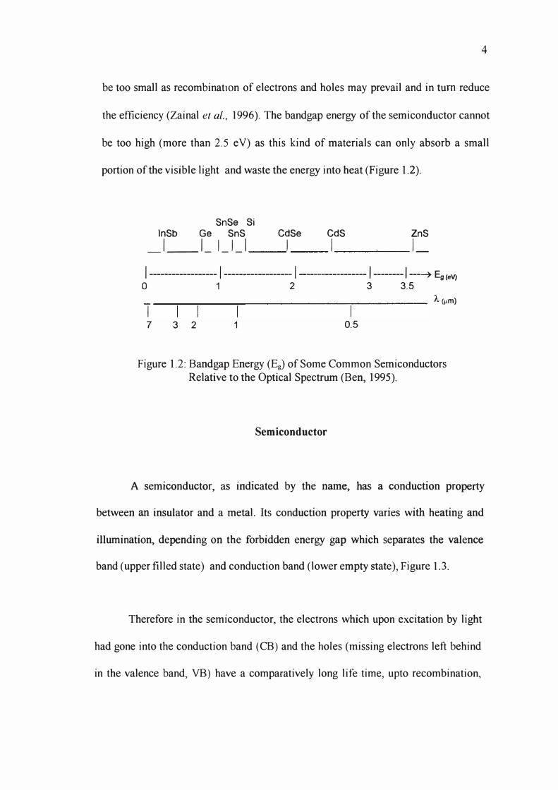
4
be too small as recombinatIOn of electrons and holes may prevail and in tum reduce
the efficiency (Zainal et al., 1 996). The bandgap energy of the semiconductor cannot
be too high (more than 2.5 eV) as this kind of materials can only absorb a small
portion ofthe visible light and waste the energy into heat (Figure 1.2).
SnSe Si InSb Ge SnS CdSe CdS ZnS 1 __ 1- 1_1_1 __ 1 __ 1 ____ 1_
1------------------1------------------1-----------------I--------I---� Eg (eV) o 1 2 3 3.5
1 _�--�----�----------------�---------- A(�m)
7 3 2 1 0.5
Figure 1.2: Bandgap Energy (Eg) of Some Common Semiconductors Relative to the Optical Spectrum (Ben, 1995).
Semiconductor
A semiconductor, as indicated by the name, has a conduction property
between an insulator and a metal. Its conduction property varies with heating and
illumination, depending on the forbidden energy gap which separates the valence
band (upper filled state) and conduction band (lower empty state), Figure 1 .3.
Therefore in the semiconductor, the electrons which upon excitation by light
had gone into the conduction band (CB) and the holes (missing electrons left behind
in the valence band, VB) have a comparatively long life time, upto recombination,

5
sufficient for them to participate In the electrochemical reaction at the
semiconductor-electrode/electrolyte interface (Yuri, 1990).
CB
~ Metal Insulator Semiconductor
Valance Band V7ZI Conduction Band 1-1 __ ..... Overlapping Band I><X><I
Figure 1 .3: The Energy gap (Eg) Difference Between the Metal, Insulator and Semiconductor
An important distinction between a metal and semiconductor has been noted
by Kavanos, 1990. In a metal, the orbitals are normally so closely packed that when
an electron is promoted from a low-lying to higher-lying orbital, the electron almost
instantaneously decays back to the lower state. In a semiconductor, the electron does
not "relax" so rapidly since it must pass over a wider bandgap. This property make
the semiconductor special and more appropriate for certain applications. Each
semiconductor is characterised by a bandgap energy, Eg. Semiconductor can absorb
photons having energy, hv > Eg . The energy of each absorbed photon is consumed
by raising an electron from the valence-band up to the conduction band and creating
an electron and hole pair (EHP). Each photon having hv greater than the Eg (up to
several E� ) is capable of generating an EHP, also known as charge carriers. Photons
with hv < Eg are basically not absorbed by the semiconductor and cannot generate

6
EHP. This fact and spectral distribution of radiation lead to the conclusion that the
carriers-generation rate per unit area is a function of Eg of the semiconductor (Hu
and White, 1983).
Semiconductors can be divided into two groups, pure and doped. The pure
semiconductors are those with their conductivity and Eg determined by their inherent
property. The doped are those with their conductivity and Eg influenced by
introducing traces of impurity atoms. By doping a pure semiconductor, the amount of
energy required to induce conduction in the semiconductor is greatly reduced. The
doped semiconductors can be subdivided into p-type (positive) and n-type (negative)
according to their electrochemical behaviour. They would manifest anodic or
cathodic photocurrent depending on their majority carrier current flow (Yuri, 1 990).
An n-type semiconductor would show anodic photocurrent as it contains electrons as
its majority carriers while a p-type shows cathodic photocurrent flow as it contains
holes as its majority carriers. Thus, the p-type induces reduction on the electrolyte
species at the semiconductor-electrolyte interface while n-type induces oxidation,
when they are deployed as photoelectrodes in the PEes.
Direct and Indirect Semiconductors
Beside the p and n-type, the semiconductor can also be direct or indirect
transition material, depending on its electronic transfer between VB and CB. In its
conduction band, the semiconductor has a low laying enef!:,'}' level (minimum, m)


