
With EMI Analyzer
Verification of Optimal EMI Filter Design
Cheol-Soo, Kim
EMCIS Co., Ltd

2
Table
1. EMI Measurement
2. Optimal EMI filter design
3. Verification of EMI Filter Design
4. Case Study
LISN
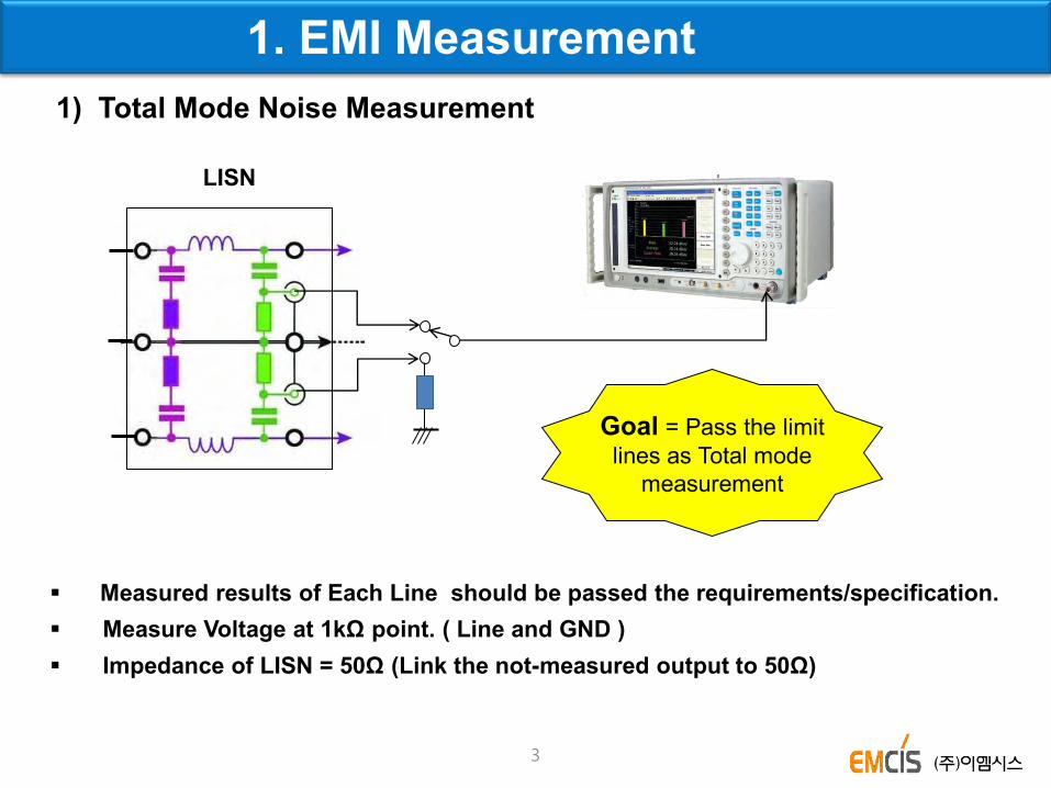
1. EMI Measurement 1) Total Mode Noise Measurement
3
Goal = Pass the limit lines as Total mode
measurement
Measured results of Each Line should be passed the requirements/specification. Measure Voltage at 1kΩ point. ( Line and GND ) Impedance of LISN = 50Ω (Link the not-measured output to 50Ω)

LISN
EMI Source (EUT)
ICM/2
IOP+IDM ICM/2
: Differential-mode (DM) noise current (IDM) path
: Common-mode (CM) noise current (ICM) path
IOP : main operating current
ICM/2+IDM ICM/2-IDM
1. EMI Measurement 1) Total Mode Noise Measurement
4
The measured results is the mixture of CM &DM Noises The measured results shown on the instruments is only the higher level between CM & DM noises

5
1. EMI Measurement 1) Total Mode Noise Measurement
- Takes a long time
- Cost up
- Larger filter sizes
Interpretation difficulties for circuit
Multi-stage filter circuit
5

2. Optimal filter design
6
1) Must-Be consideration in Optimal Filter Design
Cost
No. of Components
Size
Frame, Material of Case
Stage of Filter
Location of Filter
Ground
Additional Cost
+ Directly Linked
7
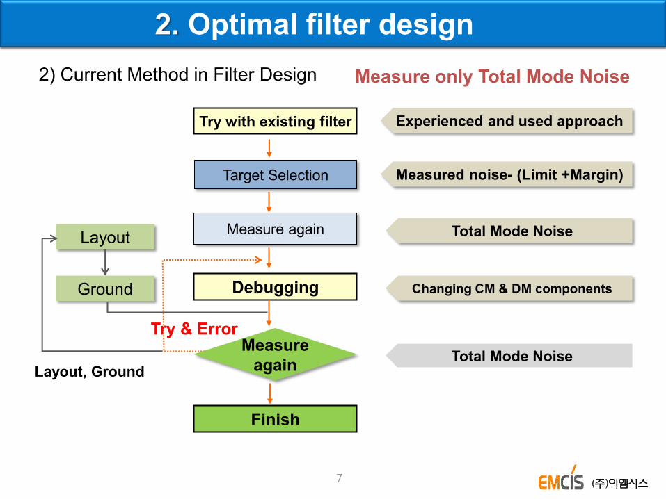
2. Optimal filter design Measure only Total Mode Noise
Try with existing filter
Debugging
Finish
Layout, Ground
Try & Error
2) Current Method in Filter Design
Measure again
Layout
Ground
Measure again
Target Selection Measured noise- (Limit +Margin)
Total Mode Noise
Changing CM & DM components
Experienced and used approach
Total Mode Noise
8
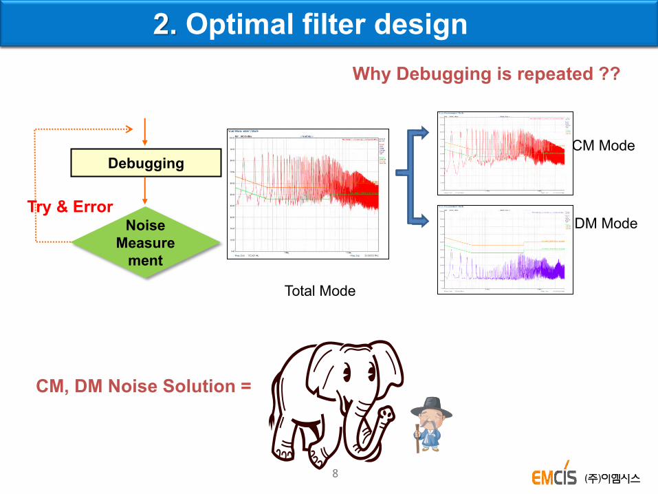
2. Optimal filter design
8
Why Debugging is repeated ??
Total Mode
CM Mode
DM Mode
Debugging
Try & Error Noise
Measurement
CM, DM Noise Solution =

9
EMI Analyzer EA-300
System
2. Optimal filter design
Impedance Module
3. Filter Design with EMI Analyzer
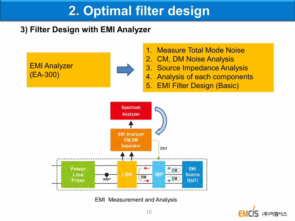
10
2. Optimal filter design
EMI Measurement and Analysis
1. Measure Total Mode Noise 2. CM, DM Noise Analysis 3. Source Impedance Analysis 4. Analysis of each components 5. EMI Filter Design (Basic)
3) Filter Design with EMI Analyzer
EMI Analyzer (EA-300)

11
2. Optimal filter design 4) EMCIS Filter Design Process
Measure Noise
Analysis of Noises
Source Impedance analysis of CM, DM
CM, DM Filter Design
Measure Noise
Finish
Layout, Frame
Ground
Target Decision
Total Mode Noise
CM, DM Mode Noise
Measured Noise- (Limit +Margin)
Impedance Analysis of each mode under EUT operation
CM Mode Filter Design
Total Mode Noise

12
2. Optimal filter design
Measure Noise
Analysis of Noise, CM and DM
Source Impedance Analysis, CM, DM
CM, DM Filter Design
Measure the
results
Finish
Layout, Frame
Ground
Target Decision
4) EMCIS Filter Design Process Total Mode Noise measurement
L1 or L2 Noise (Total Noise)
13
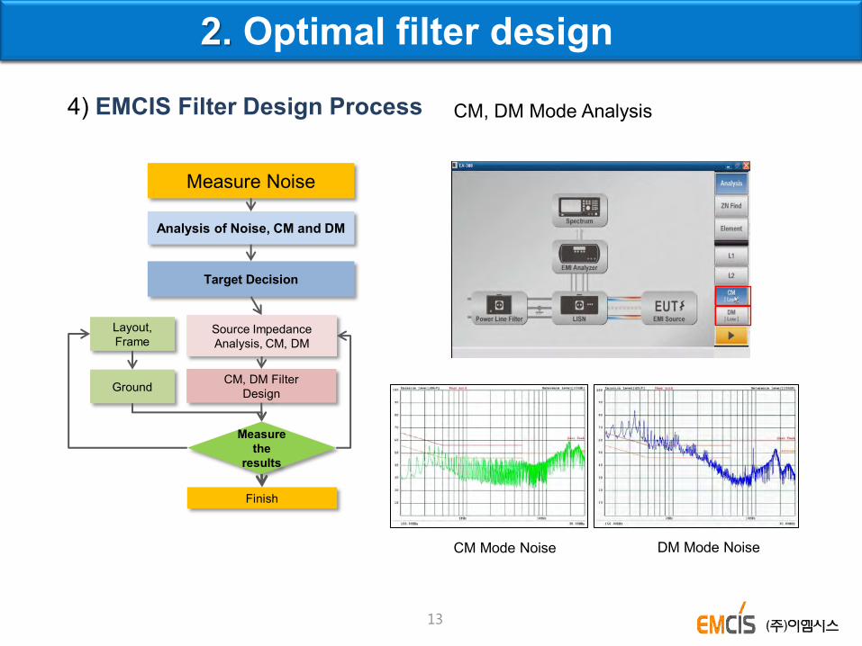
2. Optimal filter design
CM, DM Mode Analysis
DM Mode Noise CM Mode Noise
4) EMCIS Filter Design Process
Measure Noise
Analysis of Noise, CM and DM
Source Impedance Analysis, CM, DM
CM, DM Filter Design
Measure the
results
Finish
Layout, Frame
Ground
Target Decision
2. Optimal filter design
14
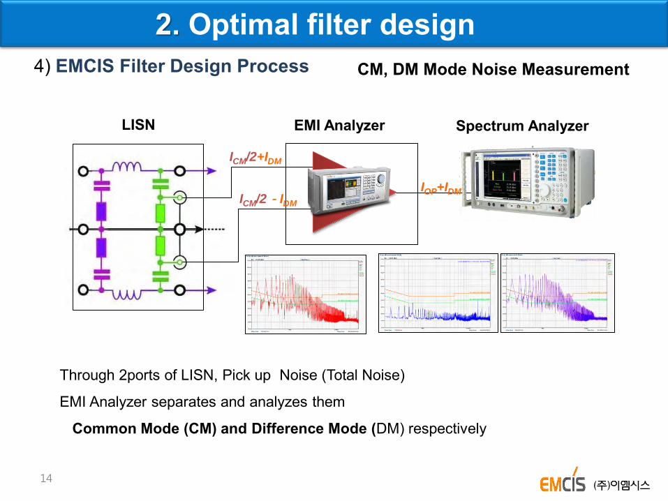
Through 2ports of LISN, Pick up Noise (Total Noise)
EMI Analyzer separates and analyzes them
Common Mode (CM) and Difference Mode (DM) respectively
ICM/2+IDM
ICM/2-IDM IOP+IDM
LISN EMI Analyzer Spectrum Analyzer
CM, DM Mode Noise Measurement 4) EMCIS Filter Design Process

15
2. Optimal filter design
200kHz Total CM Mode DM Mode
Noise Level 90dBuV 81dBuV 86dBuV
LIMIT 53dBuV 53dBuV 53dBuV
Margin 3dBuV 3dBuV 3dBuV
Insertion loss 40dBuV 31dBuV 36dBuV
Target - Solution
4) EMCIS Filter Design Process
Measure Noise
Analysis of Noise, CM and DM
Source Impedance Analysis, CM, DM
CM, DM Filter Design
Measure the
results
Finish
Layout, Frame
Ground
Target Decision

16
2. Optimal filter design Source Impedance Analysis
CM Mode 1) Select CM Mode
2) Set up Frequency
1st frequency over the Limit
Input Frequency
4) EMCIS Filter Design Process
Measure Noise
Analysis of Noise, CM and DM
Source Impedance Analysis, CM, DM
CM, DM Filter Design
Measure the
results
Finish
Layout, Frame
Ground
Target Decision
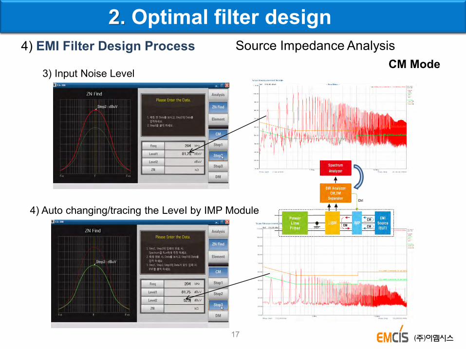
CM Mode 3) Input Noise Level
4) Auto changing/tracing the LeveI by IMP Module
17
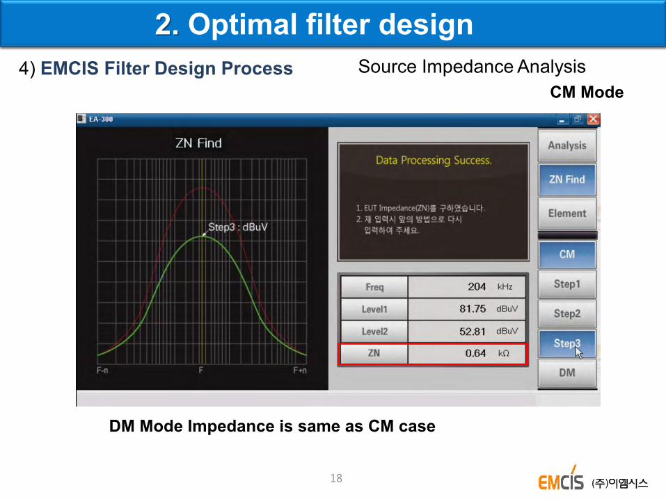
2. Optimal filter design 4) EMI Filter Design Process Source Impedance Analysis
18
2. Optimal filter design
DM Mode Impedance is same as CM case
CM Mode 4) EMCIS Filter Design Process Source Impedance Analysis

2. Optimal filter design
NV
LZ
NZ
SZ
SZ
oV
V0 LISN
EUT ZS ZN
VN
ZL
S
SN
O
N
Z
ZZL
v
vIL
22
2020)()(
loglog
4) EMCIS Filter Design Process Source Impedance Analysis
Nv
CZ
NZsZsZ
NZ
CZsZ
ov
)(
EUT V0 LISN
ZS ZC ZN
VN
S
SNNS
S
SNNS
O
N
Z
ZZZCZ
Z
ZZZsCZ
v
vIL
22 )()(log20
log20log20
CM Mode
DM Mode
20
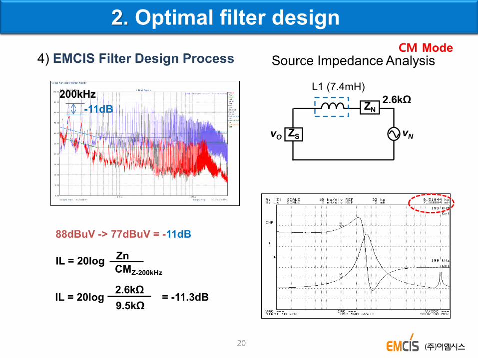
2. Optimal filter design CM Mode
4) EMCIS Filter Design Process Source Impedance Analysis
ZS
ZN
vO vN
88dBuV -> 77dBuV = -11dB
IL = 20log 2.6kΩ 9.5kΩ
= -11.3dB
Zn CMZ-200kHz
IL = 20log
2.6kΩ L1 (7.4mH)
200kHz -11dB

21
2. Optimal filter design DM Mode
87dBuV ->72dBuV = -15dB
ZS
ZN
vO vN C=0.47uF
Source Impedance Analysis
200kHz
-15dB
20log Zn XCZ - 200kHz
20log 10Ω 1.7Ω = -15.4 dB
IL =
10Ω
IL =
4) EMCIS Filter Design Process
22
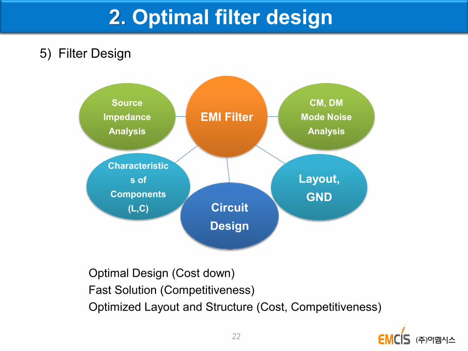
2. Optimal filter design
EMI Filter
Optimal Design (Cost down) Fast Solution (Competitiveness) Optimized Layout and Structure (Cost, Competitiveness)
5) Filter Design
Circuit Design
Source Impedance
Analysis
Characteristics of
Components (L,C)
Layout, GND
CM, DM Mode Noise
Analysis

5) EMI Filter Design (Basic)
23
2. Optimal filter design
(DM Mode) (CM Mode)

CM Mode Noise
DM Mode Noise
Total Mode Noise
1) Verifying by Noise characteristics
• Check the proper margin (from the limit line) at each mode, CM,DM, and Total Mode with EMI Analyzer
• Recommended/acceptable about 3dB margin at Low frequency range
3. Verification of EMI Filter Design

25
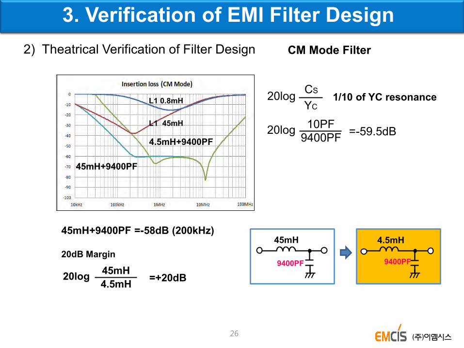
CM Mode Filter 2) Theatrical Verification of Filter Design
CM Mode Noise 38dB
ZN 2π F
Ref L = = 0.8mH (-3dB)
45mH 0.8mH 20log =-35dB =-38dB
ZS
ZN
vO
vN
1kΩ L1
21Ω L1 0.8mH
L1 45mH
CM L
Y-Cap ZS
ZN vO vN
Check the capacity of CML & Y-Capacitor is reasonable ??
200kHz
3. Verification of EMI Filter Design
26
45mH
9400PF
CM Mode Filter
45mH+9400PF
L1 0.8mH CS YC
20log 1/10 of YC resonance
9400PF 10PF 20log =-59.5dB
4.5mH+9400PF
L1 45mH
45mH+9400PF =-58dB (200kHz)
20dB Margin
4.5mH 45mH 20log =+20dB
4.5mH
9400PF
3. Verification of EMI Filter Design 2) Theatrical Verification of Filter Design
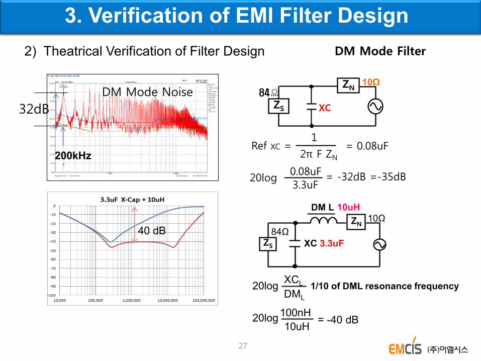
27
DM Mode Filter
DM Mode Noise
3.3uF
0.08uF 20log = -32dB =-35dB
1
2π F ZN Ref XC = = 0.08uF
32dB
10Ω
ZS
ZN
XC
84Ω
XC 3.3uF ZS
ZN
DM L 10uH
84Ω 10Ω
DML
XCL 20log
= -40 dB
200kHz
1/10 of DML resonance frequency
10uH
100nH 20log
40 dB
3. Verification of EMI Filter Design 2) Theatrical Verification of Filter Design

28
4. Case Study of EMI Filter Design
Input AC220V Output DC300V
1) Battery charger on Hybrid Vehicle
29
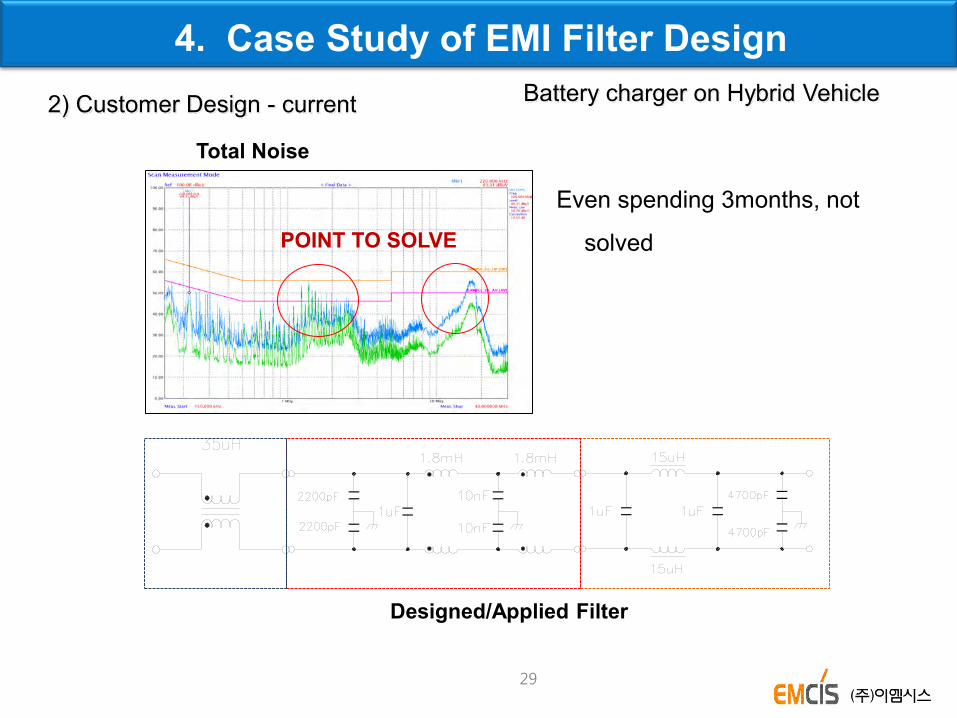
Total Noise
2) Customer Design - current
POINT TO SOLVE
Designed/Applied Filter
Even spending 3months, not
solved
4. Case Study of EMI Filter Design Battery charger on Hybrid Vehicle

30
2 Ferrite cores feed on cable
-2 turns (35uH)
3stage Filter design
4 stage Filter design
2) Customer design - current
4. Case Study of EMI Filter Design Battery charger on Hybrid Vehicle

Common Mode Differential Mode
Result : the Noise in target is determined as Common Mode Noise
3) Noise Analysis – EMCIS
4. Case Study of EMI Filter Design Battery charger on Hybrid Vehicle
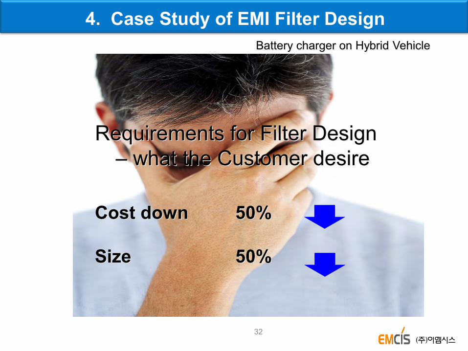
32
Requirements for Filter Design – what the Customer desire
Cost down 50% Size 50%
4. Case Study of EMI Filter Design Battery charger on Hybrid Vehicle

33
4) Measure the noises
Total Noise
60dB
Target
215kHz 112.7dBuv->53dBuV = Min 60dB deduction
Measure the current noise to decide
the target and the Filter design
33
(Meausre without any filter)
4. Case Study of EMI Filter Design Battery charger on Hybrid Vehicle

34
Common Mode Differential Mode
5) Analyze the Noise characteristics
Target
CM Mode : 215kHz 123.7dBuV -53dBuV =70dB
DM Mode : 240kHz 116.7dBuV -53dBuV =70dB
Measure each mode, CM & DM respectively
for Filter Design
34
4. Case Study of EMI Filter Design Battery charger on Hybrid Vehicle

35
C L
L C
6) Source Impedance Analysis
CM Mode Frequency 216kHz
By Pass 123dBuV Impedance Module
Control 116dBuV
Level Difference 7dB Source Impedance 7 kΩ
35
LISN
EMI Source (EUT)
ICM/2
IOP+IDM ICM/2
L
G
N CM noise
IMP
DM Mode Freq 240kHz
By Pass 116.7dBuV Impedance Module
Control 95.2dBuV
Level Difference 21.5dB Source Impedance 16.8Ω
4. Case Study of EMI Filter Design Battery charger on Hybrid Vehicle
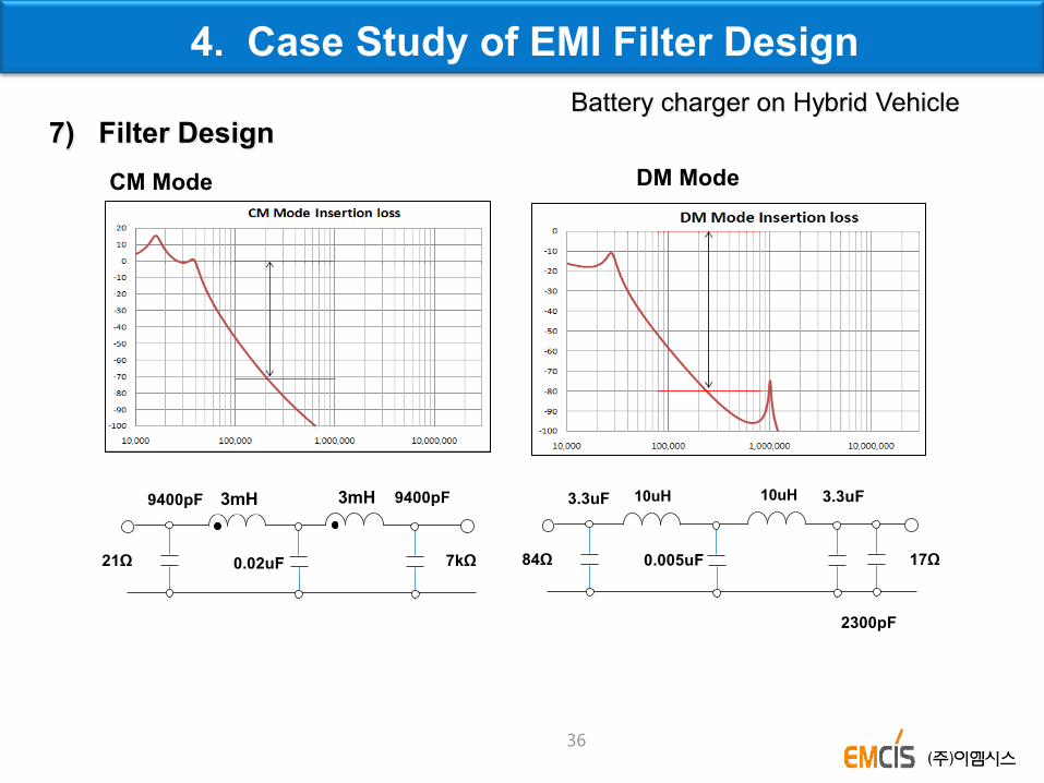
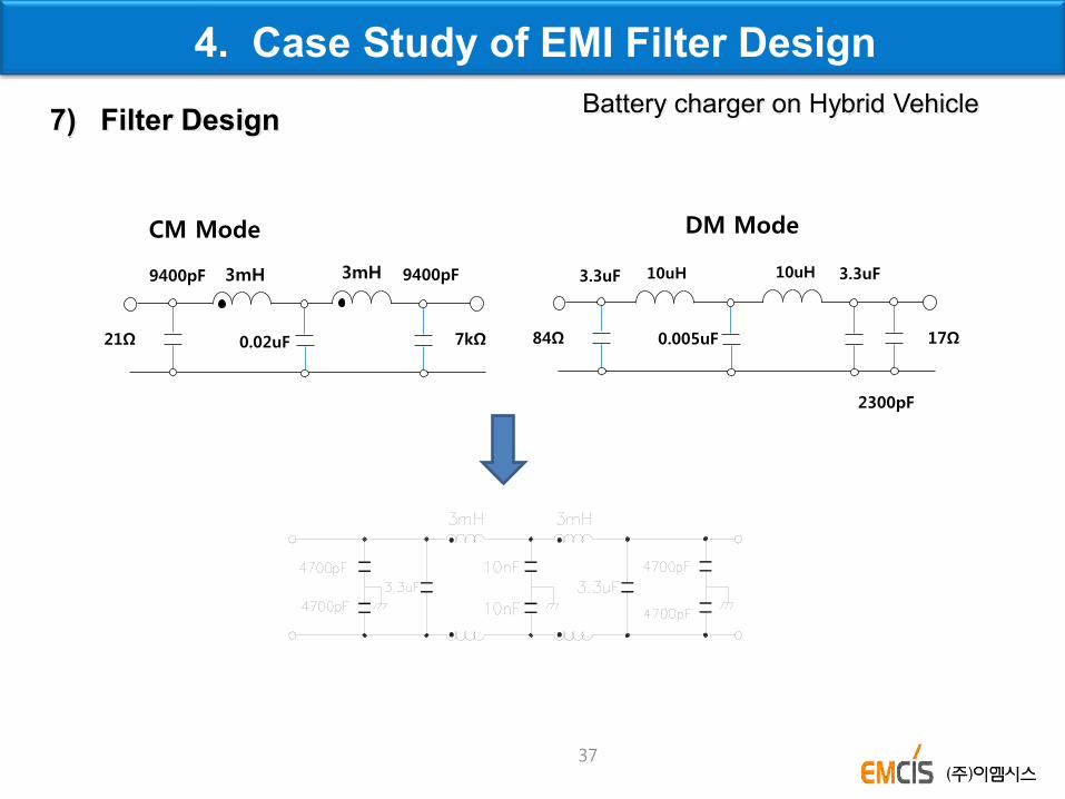
36
7) Filter Design CM Mode DM Mode
9400pF
0.02uF
3mH 3mH
21Ω
9400pF
7kΩ
3.3uF
0.005uF
10uH 10uH
84Ω
3.3uF
17Ω
2300pF
4. Case Study of EMI Filter Design Battery charger on Hybrid Vehicle
37
9400pF
0.02uF
3mH 3mH
21Ω
9400pF
7kΩ
3.3uF
0.005uF
10uH 10uH
84Ω
3.3uF
17Ω
2300pF
7) Filter Design
CM Mode DM Mode
4. Case Study of EMI Filter Design Battery charger on Hybrid Vehicle

38
The noise is over the limit line beyond 1MHz frequency
EMI Filter Design = Very Good !!!
8) Measure applying EMCIS design filter
This is the Point why EMI solution is
impossible for last 3months!!
4. Case Study of EMI Filter Design Battery charger on Hybrid Vehicle

39
Common Mode
Differential Mode
9) Analysis of the Pointed range
Results – the Cause 1. the problem is by Common Mode Noise 2. Ground
4. Case Study of EMI Filter Design Battery charger on Hybrid Vehicle
Measure Noise
Analysis of Noise, CM and DM
Source Impedance Analysis, CM, DM
CM, DM Filter Design
Measure the
results
Finish
Layout, Frame
Ground
Target Decision

40
* Delete 472Y-CAP * The purpose of Y-Cap in input portion : Coupling noise elimination caused by layout
Total Noise : L1, L2
10) Circuit modification
4. Case Study of EMI Filter Design Battery charger on Hybrid Vehicle

41
11) Conclusion
Before After
4. Case Study of EMI Filter Design Battery charger on Hybrid Vehicle

42
Target 215kHz 112.7dBuv->53dBuV 59.7dB ≒ 60dB이상
Result 215kHz 112.7dBuv->43dBuV 69.7dB ≒ 70dB
70dB 80dB
70dB
11) Conclusion
42
4. Case Study of EMI Filter Design Battery charger on Hybrid Vehicle

43
Thank you


