
Voltage translationHow to manage mixed-voltage designswith NXP level translators
2 Voltage translation — How to manage mixed-voltage designs using NXP level translators Voltage translation — How to manage mixed-voltage designs using NXP level translators 3
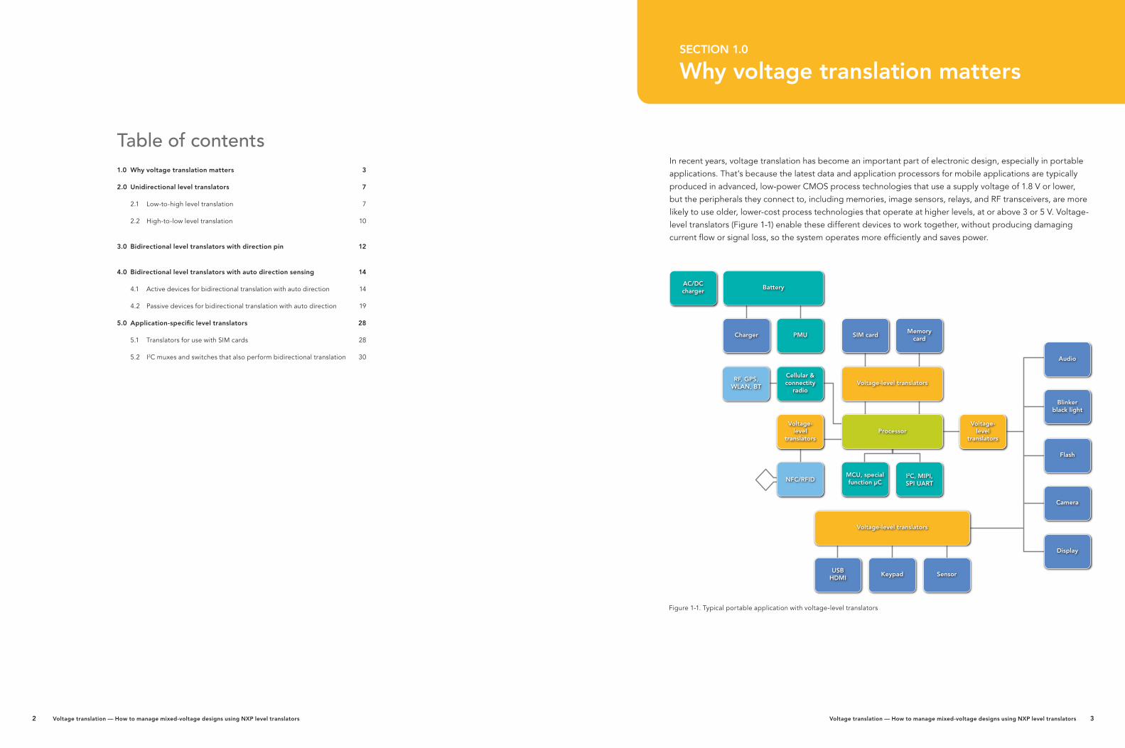
In recent years, voltage translation has become an important part of electronic design, especially in portable applications. That’s because the latest data and application processors for mobile applications are typically produced in advanced, low-power CMOS process technologies that use a supply voltage of 1.8 V or lower, but the peripherals they connect to, including memories, image sensors, relays, and RF transceivers, are more likely to use older, lower-cost process technologies that operate at higher levels, at or above 3 or 5 V. Voltage-level translators (Figure 1-1) enable these different devices to work together, without producing damaging current flow or signal loss, so the system operates more efficiently and saves power.
AC/DCcharger
NFC/RFID
RF, GPS,WLAN, BT
Cellular &connectity
radio
Processor
SIM cardMemory
card
Blinkerblack light
Audio
Flash
Camera
Display
USBHDMI
Keypad Sensor
MCU, specialfunction µC
I2C, MIPI,SPI UART
Voltage-level translators
Voltage-level translators
Voltage-level
translators
Voltage-level
translators
Battery
Charger PMU
Figure 1-1. Typical portable application with voltage-level translators
Why voltage translation mattersSECTION 1.0
Table of contents1.0 Why voltage translation matters 3
2.0 Unidirectional level translators 7
2.1 Low-to-high level translation 7
2.2 High-to-low level translation 10
3.0 Bidirectional level translators with direction pin 12
4.0 Bidirectional level translators with auto direction sensing 14
4.1 Active devices for bidirectional translation with auto direction 14
4.2 Passive devices for bidirectional translation with auto direction 19
5.0 Application-specific level translators 28
5.1 Translators for use with SIM cards 28
5.2 I2C muxes and switches that also perform bidirectional translation 30

4 Voltage translation — How to manage mixed-voltage designs using NXP level translators Voltage translation — How to manage mixed-voltage designs using NXP level translators 5
A quick overview
In most mixed-voltage designs, the output voltage level of a driver device needs to be shifted up or down so that the receiver device can interpret it correctly, or vice versa (Figure 1-2).
There are often variations in the logic switching input (VIH and VIL) and the output levels (VOH and VOL) for commonly used logic devices in the range of 3 and 5 V (Figure 1-3).
When the driver VOH is less than the receiver VIH, and/or the driver VOL is greater than the receiver VIL, system behavior becomes unpredictable (Figure 1-4).
Configuring the system to translate voltages from high to low or from low to high, according to the recommended guidelines for the input and output voltage levels of each component, makes the system more predictable, improves overall performance, and saves energy.
Unidirectional and bidirectional devices
Devices that translate voltages from low to high levels or from high to low levels also transfer data. The data transfer can work in one direction (unidirectional) or in two directions (bidirectional). Figure 1-5 shows a digital camera that uses the NXP 74AUP1T45, a bidirectional level translator, to translate between the color processor, which uses 1.8 V signals, and the memory subsystem, which uses 3.3 V signals.
Some bidirectional translators have a direction pin (DIR) to control the direction of data. Others have DIR and Output Enable (OE) pins for tri-stating the output. Another feature, called auto-direction sensing has no DIR pin, and this helps reduce the number of control pins required in the system for data flow.
Devices for level translation and signal switching
In situations that need voltage translation and signal switching, a crossbar switch equipped with a diode can be used.
0.0 V
0.5 V
1.0 V
1.5 V
2.0 V
2.5 V
3.0 V
3.5 V
4.0 V
4.5 V
5.0 V
1.2 VCMOS
1.8 VCMOS
3 VBiCMOS
5 VBiCMOS
3 VCMOS
5 VTTL/CMOS
5 VCMOS
Undefined region: behavior of system is unpredictable
3.4 V
2.0 V
1.5 V
0.8 V
0.35 V
5 V
3.6 V
2.0 V
2.5 V
0.55 V
1.08 V
1.5 V
0.275 V
1.2 V
0.47 V0.5 V0.78 V0.825 V
1.8 V
0.31 V
0.63 V
0.9 V1.17 V1.35 V
3.6 V
2.0 V
3.4 V
0.4 V0.5 V
1.5 V
5 V
4.5 V
3.5 V
2.5 V
1.5 V
0.4 V
5 V
2.0 V
1.5 V
0.8 V
0.4 V
4.7 V
VCC
VOH
VIH
VT
VIL
VOL
Vol1 < VII1
Vol > VIIVOH < VIH
Figure 1-4. Incompatible voltages can cause unpredictable system behavior
TT
TT
Driver
Receiver
Receiver3.3 V
3.3 V
1.8 V
1.8 V
3.3 V
1.8 V
Driver
Figure 1-2. Shifting the output voltage level up or down
SDRAM74AUP1T45
1.8 V
1.8 V
3.3 V
3.3 V
Colorprocessor
Figure 1-5. Low-to-high level translation in a digital camera0.0 V
0.5 V
1.0 V
1.5 V
2.0 V
2.5 V
3.0 V
3.5 V
4.0 V
4.5 V
5.0 V
1.2 VCMOS
1.8 VCMOS
3 VBiCMOS
5 VBiCMOS
3 VCMOS
5 VTTL/CMOS
5 VCMOS
3.4 V
2.0 V
1.5 V
0.8 V
0.35 V
5 V
3.6 V
2.0 V
2.5 V
0.55 V
1.08 V
1.5 V
0.275 V
1.2 V
0.47 V0.5 V0.78 V0.825 V
1.8 V
0.31 V
0.63 V
0.9 V1.17 V1.35 V
3.6 V
2.0 V
3.4 V
0.4 V0.5 V
1.5 V
5 V
4.5 V
3.5 V
2.5 V
1.5 V
0.4 V
5 V
2.0 V
1.5 V
0.8 V
0.4 V
4.7 V
VCC
VOH
VIH
VT
VIL
VOL
Figure 1-3. Switching input and output levels for 3 V and 5 V logic devices

6 Voltage translation — How to manage mixed-voltage designs using NXP level translators Voltage translation — How to manage mixed-voltage designs using NXP level translators 7
Find the right translator for your designNXP offers level translators for specific protocols and translators that work in general-purpose applications. This guide can help you find the right one for your design.
Table 1-1 lists the families available from NXP. Active devices include a CMOS output stage with a specific source and sink currents. Passive devices do not have CMOS outputs; the sink and source currents come from the supply voltage.
Table 1-1. NXP level translators
Type Drive NXP families Description
Unidirectional Active
AHC, ALVC, ALVT, AUP, HC, HEF, LV, LVC
Suitable for use as low-to-high or high-to-low translators, these are standard logic devices with features like low-threshold inputs, open-drain outputs, TTL inputs, input-clamping diodes, current-limiting resistors, and overvoltage-tolerant inputs.
Bidirectional with direction pin
Active
ALVC, AUP, AVCnTGTL, LVCnT*
These devices perform bidirectional level translation and have a direction pin that sets the direction of the data flow. The AUP, AVC, and LVC families are for general-purpose voltage translation in the range from 0.8 to 5.5 V. GTL level translators are specially designed to support GTL logic, which is widely used on processors. They convert GTL levels to LVTTL levels.
Bidirectional with auto direction sensing
Active NTB, PCA These devices perform bidirectional level translation without a direction pin. The NTB and NTS translators integrate one-shot edge accelerators and are suitable for use with open-drain outputs. The NTB and PCA families support buffered outputs. The NTS and NTB families have integrated pull-ups, and are a good choice for applications that use interfaces based on I2C, SMBus, SPI, or UARTs. CBTD and CBTLVD devices are bus switches that also perform level translation.
PassiveCBTD, CBTLVD, GTL, NTS, NVT
Application-specific
ActiveNVT level shifters for SIM cards
The NVT SIM card level shifters contain an LDO that can deliver two different voltages, from a typical mobile phone battery voltage, and convert the data, RSTn and CLKn signals between a SIM card and a host microcontroller.
PassivePCA muxes and switches for I2C
These multiplexers and switches split the I2C-bus into several branches, so the I2C master can select and address multiple identical devices without address conflicts. They also permit a single master to interface with multiple devices with different power-supply voltages.
*n = 1, 2, 4, 8, or 16 channelsThe rest of this guide provides details and recommendations for each type.
Many of NXP’s standard logic devices include features that let them be used as unidirectional translators that perform low-to-high or high-to-low level translation.
The relevant product families include AHC, ALVC, ALVT, AUP, HC, HEF, LV, and LVC. This covers devices with features like low-threshold inputs, open-drain outputs, TTL inputs, input-clamping diodes, current-limiting resistors, and overvoltage-tolerant inputs. They are active devices that have a CMOS output stage with specific source and sink currents.
2.1 Low-to-high level translationLogic devices equipped with low-threshold inputs or open-drain outputs can be used for low-to-high level translation.
Devices with low-threshold inputs
CMOS devices with input switching thresholds lower than the typical values can be used for low-to-high translation. Several NXP families are equipped with low-threshold inputs (Figure 2-1).
Unidirectional level translatorsSECTION 2.0
VCC
To logic circuit
P1
D1
P2
GND
N1
ESD protection
Figure 2-1. Simplified CMOS input with lower-than-typical threshold values
8 Voltage translation — How to manage mixed-voltage designs using NXP level translators Voltage translation — How to manage mixed-voltage designs using NXP level translators 9
The combination of N1 sizing and the drop across diode D1 determines the input threshold. Also, the P2 PMOS reduces cross-bar current through the inverter.
The AHC(T) and HCT series operate in the 5 V range and can be used to interface with 3.3 V outputs. The AUP1T and NX3 series operate in the 3.6 V range and can be used to interface with 1.8 V outputs.
Devices with open-drain outputs
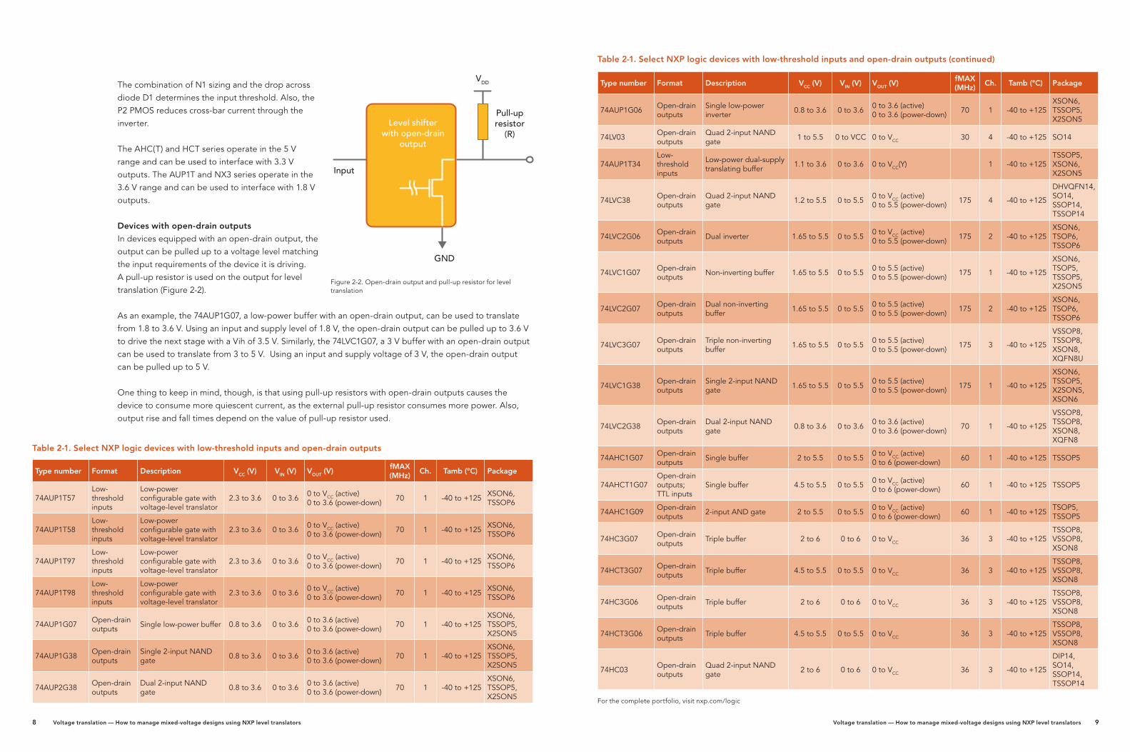
In devices equipped with an open-drain output, the output can be pulled up to a voltage level matching the input requirements of the device it is driving. A pull-up resistor is used on the output for level translation (Figure 2-2).
As an example, the 74AUP1G07, a low-power buffer with an open-drain output, can be used to translate from 1.8 to 3.6 V. Using an input and supply level of 1.8 V, the open-drain output can be pulled up to 3.6 V to drive the next stage with a Vih of 3.5 V. Similarly, the 74LVC1G07, a 3 V buffer with an open-drain output can be used to translate from 3 to 5 V. Using an input and supply voltage of 3 V, the open-drain output can be pulled up to 5 V.
One thing to keep in mind, though, is that using pull-up resistors with open-drain outputs causes the device to consume more quiescent current, as the external pull-up resistor consumes more power. Also, output rise and fall times depend on the value of pull-up resistor used.
Type number Format Description VCC (V) VIN (V) VOUT (V)fMAX (MHz)
Ch. Tamb (°C) Package
74AUP1T57Low-threshold inputs
Low-power configurable gate with voltage-level translator
2.3 to 3.6 0 to 3.6 0 to VCC (active) 0 to 3.6 (power-down) 70 1 -40 to +125 XSON6,
TSSOP6
74AUP1T58Low-threshold inputs
Low-power configurable gate with voltage-level translator
2.3 to 3.6 0 to 3.6 0 to VCC (active) 0 to 3.6 (power-down) 70 1 -40 to +125 XSON6,
TSSOP6
74AUP1T97Low-threshold inputs
Low-power configurable gate with voltage-level translator
2.3 to 3.6 0 to 3.6 0 to VCC (active) 0 to 3.6 (power-down) 70 1 -40 to +125 XSON6,
TSSOP6
74AUP1T98Low-threshold inputs
Low-power configurable gate with voltage-level translator
2.3 to 3.6 0 to 3.6 0 to VCC (active) 0 to 3.6 (power-down) 70 1 -40 to +125 XSON6,
TSSOP6
74AUP1G07 Open-drain outputs Single low-power buffer 0.8 to 3.6 0 to 3.6 0 to 3.6 (active)
0 to 3.6 (power-down) 70 1 -40 to +125XSON6, TSSOP5, X2SON5
74AUP1G38 Open-drain outputs
Single 2-input NAND gate 0.8 to 3.6 0 to 3.6 0 to 3.6 (active)
0 to 3.6 (power-down) 70 1 -40 to +125XSON6, TSSOP5, X2SON5
74AUP2G38 Open-drain outputs
Dual 2-input NAND gate 0.8 to 3.6 0 to 3.6 0 to 3.6 (active)
0 to 3.6 (power-down) 70 1 -40 to +125XSON6, TSSOP5, X2SON5
Table 2-1. Select NXP logic devices with low-threshold inputs and open-drain outputs
Table 2-1. Select NXP logic devices with low-threshold inputs and open-drain outputs (continued)
Input
VDD
GND
Pull-upresistor
(R)Level shifter
with open-drainoutput
Figure 2-2. Open-drain output and pull-up resistor for level translation
Type number Format Description VCC (V) VIN (V) VOUT (V)fMAX (MHz)
Ch. Tamb (°C) Package
74AUP1G06 Open-drain outputs
Single low-power inverter 0.8 to 3.6 0 to 3.6 0 to 3.6 (active)
0 to 3.6 (power-down) 70 1 -40 to +125XSON6, TSSOP5, X2SON5
74LV03 Open-drain outputs
Quad 2-input NAND gate 1 to 5.5 0 to VCC 0 to VCC 30 4 -40 to +125 SO14
74AUP1T34Low-threshold inputs
Low-power dual-supply translating buffer 1.1 to 3.6 0 to 3.6 0 to VCC(Y) 1 -40 to +125
TSSOP5, XSON6, X2SON5
74LVC38 Open-drain outputs
Quad 2-input NAND gate 1.2 to 5.5 0 to 5.5 0 to VCC (active)
0 to 5.5 (power-down) 175 4 -40 to +125
DHVQFN14, SO14, SSOP14, TSSOP14
74LVC2G06 Open-drain outputs Dual inverter 1.65 to 5.5 0 to 5.5 0 to VCC (active)
0 to 5.5 (power-down) 175 2 -40 to +125XSON6, TSOP6, TSSOP6
74LVC1G07 Open-drain outputs Non-inverting buffer 1.65 to 5.5 0 to 5.5 0 to 5.5 (active)
0 to 5.5 (power-down) 175 1 -40 to +125
XSON6, TSOP5, TSSOP5, X2SON5
74LVC2G07 Open-drain outputs
Dual non-inverting buffer 1.65 to 5.5 0 to 5.5 0 to 5.5 (active)
0 to 5.5 (power-down) 175 2 -40 to +125XSON6, TSOP6, TSSOP6
74LVC3G07 Open-drain outputs
Triple non-inverting buffer 1.65 to 5.5 0 to 5.5 0 to 5.5 (active)
0 to 5.5 (power-down) 175 3 -40 to +125
VSSOP8, TSSOP8, XSON8, XQFN8U
74LVC1G38 Open-drain outputs
Single 2-input NAND gate 1.65 to 5.5 0 to 5.5 0 to 5.5 (active)
0 to 5.5 (power-down) 175 1 -40 to +125
XSON6, TSSOP5, X2SON5, XSON6
74LVC2G38 Open-drain outputs
Dual 2-input NAND gate 0.8 to 3.6 0 to 3.6 0 to 3.6 (active)
0 to 3.6 (power-down) 70 1 -40 to +125
VSSOP8, TSSOP8, XSON8, XQFN8
74AHC1G07 Open-drain outputs Single buffer 2 to 5.5 0 to 5.5 0 to VCC (active)
0 to 6 (power-down) 60 1 -40 to +125 TSSOP5
74AHCT1G07Open-drain outputs; TTL inputs
Single buffer 4.5 to 5.5 0 to 5.5 0 to VCC (active) 0 to 6 (power-down) 60 1 -40 to +125 TSSOP5
74AHC1G09 Open-drain outputs 2-input AND gate 2 to 5.5 0 to 5.5 0 to VCC (active)
0 to 6 (power-down) 60 1 -40 to +125 TSOP5, TSSOP5
74HC3G07 Open-drain outputs Triple buffer 2 to 6 0 to 6 0 to VCC 36 3 -40 to +125
TSSOP8, VSSOP8, XSON8
74HCT3G07 Open-drain outputs Triple buffer 4.5 to 5.5 0 to 5.5 0 to VCC 36 3 -40 to +125
TSSOP8, VSSOP8, XSON8
74HC3G06 Open-drain outputs Triple buffer 2 to 6 0 to 6 0 to VCC 36 3 -40 to +125
TSSOP8, VSSOP8, XSON8
74HCT3G06 Open-drain outputs Triple buffer 4.5 to 5.5 0 to 5.5 0 to VCC 36 3 -40 to +125
TSSOP8, VSSOP8, XSON8
74HC03 Open-drain outputs
Quad 2-input NAND gate 2 to 6 0 to 6 0 to VCC 36 3 -40 to +125
DIP14, SO14, SSOP14, TSSOP14
For the complete portfolio, visit nxp.com/logic

10 Voltage translation — How to manage mixed-voltage designs using NXP level translators Voltage translation — How to manage mixed-voltage designs using NXP level translators 11
2.2 High-to-low level translationThis category includes devices with overvoltage-tolerant inputs and devices with input-clamping diodes and current-limiting resistors.
When a driver is operating at a supply voltage higher than that of the receiver, the output voltage level of the driver must be lowered to match the input switching thresholds of the receiver (Figure 2-3). This protects the inputs of the receiver from over- and undervoltage conditions, and from overcurrent conditions. The output impedance of the driver should be matched to the impedance of the cable/trace so that there are no reflections from the receiver side. Integrated ESD protection also helps to suppress the unwanted transients due to overvoltage on the trace.
Devices with input-clamping diodes and current-limiting resistors
On some logic devices, the inputs have input clamping diodes to VCC and to GND (Figure 2-4). The input clamping diodes serve as overvoltage and ESD protection. When using CMOS devices that have current-limiting resistors at the inputs, the input voltage can exceed maximum specified values as long as the maximum current rating is observed.
In some cases, especially in industrial and automotive applications, the logic device may need to interface with voltages far above the normal 5 V limit. In these cases, choose logic devices with input-clamping diodes and use current-limiting resistors. NXP’s LV, HC, and HEF families have input-clamping diodes to VCC and can be used with current-limiting resistors for high-to-low level translation.
Devices with overvoltage-tolerant inputs
Newer ESD structures eliminate the diode to VCC and use a grounded NMOS (Figure 2-5). Without the diode, any voltage within the limits of the manufacturing process can be applied to the input without opening a current path to VCC. As a result, logic levels that exceed the device’s power supply can be applied to the inputs without impacting the application.
Since devices with overvoltage-tolerant inputs can tolerate a VIN higher than VCC, and outputs swing to VCC only, they make good choices for high-to-low level translation. The NXP LVC, LVT, ALVT, and AHC(T) families have inputs that are overvoltage-tolerant to 5.5 V, as long as input and output current ratings are observed. The inputs of AUP and AVC devices are tolerant to 3.6 V, making them suitable for designs that use a mix of 1.8 and 3.3 V devices.
VCC = 3V
ESDprotection
Overvoltage-tolerant CMOS input
Output buffer Input buffer
CableConnectorGND GND
Figure 2-3. High-to-low level translation
VCC = 3 V
GND
ESDprotection
Overvoltage-tolerant CMOS input
Input buffer
Figure 2-5. Diode-free ESD protection with an overvoltage-tolerant input
Clamping diode
VCC
GND
Input buffer
ESDprotection
RCC (min) =
VCC = 15 V
Device A
RCL
15 V - (5.0 V = 0.7 V)
IIK
IIK is found in the limiting values table of the datasheet
Figure 2-4. Using current-limiting resistors to enable high-to-low level translation
Type number Format Description VCC (V)
Output drive
capability (mA)
tpd (ns)
Rth(j-a) (K/W)
Ψth(j-top) (K/W)
Tamb (°C) Package
74AHC157 Overvoltage-tolerant inputs
Quad 2-input multiplexer 2.0 to 5.5 ±8 3.2 58 30 -40 to +125 DHVQFN16,
SO16, TSSOP16
74AUP2G157 Overvoltage-tolerant inputs
Single 2-input multiplexer 1.1 to 3.6 1.9/-1.9 3.4 206 51 -40 to +125 VSSOP8, XSON8,
XQFN8U
74LV00 Current-limiting resistors
Quad 2-input NAND gate 1.0 to 5.5 ±12 7 61 32 -40 to +125
DHVQFN14, SO14, SSOP14, TSSOP14, DIP14
74LV03 Current-limiting resistors
Quad 2-input NAND gate; open-drain 1.0 to 5.5 ±12 8 127 13 -40 to +125 SO14
74HC02 Current-limiting resistors
Quad 2-input NOR gate 2.0 to 6.0 ±5.2 7 61 32 -40 to +125
DHVQFN14, SO14, SSOP14, TSSOP14, DIP14
74ALVC74 Overvoltage-tolerant inputs
Dual D-type flip-flop with set and reset; positive-edge trigger
1.65 to 3.6 ±24 2.3 61 32 -40 to +85 DHVQFN14, SO14, TSSOP14
74AHC1G86 Overvoltage-tolerant inputs
2-input EXCLUSIVE-OR gate 2.0 to 5.5 ±8 3.4 250 69 -40 to +125 TSOP5, TSSOP5
74ALVT162244 Overvoltage-tolerant inputs
16-bit buffer/line driver with bus hold and 30 Ω termination resistors (3-state)
2.3 to 3.6 ±12 2.2 104 23 -40 to +85 TSSOP48, SSOP48
74HEF4104BP Overvoltage-tolerant inputs
Quad low-to-high voltage translator (3-state)
3.0 to 15.0 CMOS ±2.4 -40 to +85 DIP16, SO16
For the complete portfolio, visit nxp.com/logic
Table 2-2. Select NXP logic devices with overvoltage-tolerant inputs or current-limiting resistors

12 Voltage translation — How to manage mixed-voltage designs using NXP level translators Voltage translation — How to manage mixed-voltage designs using NXP level translators 13
Voltage translators that are equipped with two supply voltages, each supporting a different voltage range, can be used to translate from low to high or from high to low, and are typically available in versions that support either unidirectional or bidirectional level translation.
The devices in this section use the DIR pin to control the direction of translation, from the A to the B port or from the B to the A port. Integrated IOFF circuitry eliminates damaging backflow current when outputs are disabled during suspend or power-down mode. They are active translators, meaning they have a CMOS output stage with specific source and sink currents.
Bidirectional translators equipped with a direction pin are available with the NXP AUP, AVC, LVC, and ALVC families. These families support mixed-voltage designs ranging from 0.8 to 5.5 V. The output signals of one device can be translated from high to low or from low to high as needed to match the input thresholds. There are versions for unidirectional and bidirectional level translation. Options include formats of 1, 2, 4, 8, or 16 bits, covering the translation range of 0.8 to 3.6 V and 1.2 to 5.5 V. The result is complete coverage for designs that use supply voltages of 1.2, 1.8, 2.5, 3.3, and 5.0 V.
Bus-hold circuit
Products with an “H” in the type designation have a bus-hold circuit (Figure 3-1) that ensures a defined logic level when inputs are floating. This prevents the input voltage from floating near the threshold voltage, which can damage the device.
Figure 3-1. Bus-hold circuit of newer CMOS families
Active bus-hold circuitry in the LVC and AVC families prevents floating inputs by holding unused data inputs at a valid logic level. The bus-hold circuit acts as an input latch, retaining the last data driven if inputs are tri-stated or held in high impedance. When power is initially applied the logic state of the bus-hold latch is not guaranteed; it may power-up high or low. If a default logic state is required, external resistors will also be required, and these should be sized to overdrive the input’s bus-hold current to avoid contention issues. Details on the use of bus-hold circuits can be found in product data sheets and in application note AN240.
GTL-to-LVTTL level translators and transceivers
Gunning transceiver logic (GTL) is a type of logic signaling used to drive electronic backplane buses. Defined by the JEDEC standard JESD 8-3, GTL has a voltage swing between 0.4 and 1.5 V — much lower than that used in TTL and CMOS logic — and performs symmetrical parallel resistive termination.
GTL is often found in front-side buses based on the Intel architecture. For GTL signals to be compatible with the rest of the system, GTL levels need to be translated to low-voltage TTL (LVTTL). NXP offers a complete range of dedicated translators and transceivers for the GTL format.
Bidirectional level translators with direction pin
SECTION 3.0
Internalcircuit
Input
GND
D1 D4
D3
Q1
VCC
Q2 Q4
Q3
Type number DescriptionOperating range (V)
LVTTL 5 V tolerance
Package name
GTL2005 4-bit GTL/GTL+ to LVTTL/TTL bidirectional non-latched translator 3.0 to 3.6 Yes TSSOP14
GTL2006 13-bit GTL–/GTL/GTL+ to LVTTL translator 3.0 to 3.6 No TSSOP28
GTL2007 12-bit GTL to LVTTL translator 3.0 to 3.6 No TSSOP28
GTL2008 12-bit GTL to LVTTL translator with high impedance LVTTL and GTL outputs 3.0 to 3.6 No TSSOP28
GTL2012 2-bit LVTTL to GTL transceiver 3.0 to 3.6 Yes (Input only) TSSOP8, VSSOP8
GTL2014 4-bit LVTTL to GTL transceiver 3.0 to 3.6 Yes (Input only) TSSOP14
GTL2018 8-bit LVTTL to GTL transceiver 3.0 to 3.6 Yes (Input only) TSSOP24
GTL2034 4-bit GTL to GTL buffer 3.0 to 3.6 No TSSOP14
GTL2107 12-bit GTL-/GTL/GTL+ to LVTTL translator 3.0 to 3.6 No TSSOP28
For the complete portfolio, visit nxp.com/logic
Table 3-1. Select NXP devices for GTL-to-LVTTL translation

14 Voltage translation — How to manage mixed-voltage designs using NXP level translators Voltage translation — How to manage mixed-voltage designs using NXP level translators 15
These are dual-supply translators that use the DIR and OE pins to tri-state the output. They automatically sense the direction of the data flow. This eliminates the need for an external direction pin and the associated control logic. Auto-direction sensing makes these devices especially suited for applications where the microcontroller doesn’t have enough GPIO to change the direction of data flow, since the translators can be added to the design without external GPIO extenders or multiplexers on the PCB.
Level translators with auto direction sensing are available in active and passive formats. The active devices have a CMOS output stage with a specific source and sink. The passive devices do not have CMOS outputs; the sink and source currents come from the supply voltage.
4.1 Active devices for bidirectional level translation with auto directionPCA series: Level-translating buffers for I2C applications
Systems that use I2C (and SMBus or similar) devices operating at different voltage levels may need to be attached to a common bus. PCA series devices translate between 1 and 5 V, allowing devices specified for different voltages to be connected to the same bus. For example, a 5 V I2C master on one segment of the bus can communicate with a 1.8 V (non 5 V-tolerant) SMBus device on a different segment.
PCA devices use channel pass gates to limit the high voltage for the device output. This makes it possible for each pair to use a different bus voltage. The I2C device maintains its functions and operating mode during the level shift, and the dual supply pins can be powered up in any sequence. When any of the supply pins are unpowered, the 5 V-tolerant I/O are high-impedance.
Some PCA devices are specifically designed for level-shifting applications. They are bidirectional and require no direction control. The level-shifting bus buffers support two I2C (or SMBus) branches of up to 400 pF (Figure 4-1). They can be used to extend the bus to support loads larger than the 400 pF maximum. The bus can be extended with more devices or longer bus lengths, or both. There will be a delay equal to TPROP between the external devices. PCA devices are multi-master capable and support arbitration and bus contention on any segment.
Figure 4-1. Typical application of PCA level-shifting bus buffer
PCA devices can be used to extend or isolate the bus, and can be configured to use the internal current source to replace a pull-up resistor. See NXP application note AN10418.
NTB level shifters: Bidirectional level translation with auto-direction sensing
NTB level shifters (Figure 4-2) are ideal for use as push-pull or CMOS-type drivers that drive long-trace, capacitive, or high-impedance loads in applications that use SPI, Secure Digital, or UART interfaces.
Bidirectional level translators with auto direction sensing
SECTION 4.0
Bus ABus B
Bus master400 kHz
Slave400 kHz
PCA9517A
SDA
SCL
SDAB
SCLB
EN
SDAA
SCLA
SDA
SCL
3.3 V 1.2 V
VCC (A)VCC (B)
10 k 10 k 10 k 10 k
Type number Description VCC(A) (V) VCC(B) (V) ChannelsA-side offset
B-side offset
Package name
PCA9507 2.7 V-to-5.5 V level shifter 2.7 to 5.5 2.7 to 5.5 2 Normal Static offset SO8,
TSSOP8
PCA95080.9 V-to-5.5 V level shifter with offset free hot-swap
0.9 to 5.5 2.7 to 5.5 2 Normal Static offset SO8, TSSOP8
PCA9509 1.0 V-to-5.5 V level shifter
1.1 to (VCC(B) - 1) 3.0 to 5.5 2 Static offset Normal
SO8, TSSOP8, XQFN8
PCA9517A 0.9 V-to-5.5 V level shifter 0.9 to 5.5 2.7 to 5.5 2 Normal Static offset
SO8, TSSOP8, HWSON8
PCA9519 1.1 V-to-5.5 V quad level shifter
1.1 to (VCC(B) - 1) 3.0 to 5.5 4 Static offset Normal TSSOP20,
HVQFN24
PCA9527 3.0 V-to-5.5 V level shifter 2.7 to 5.5 2.7 to 3.6 3 Normal Static offset TSSOP10
PCA9617A 0.8 V-to-5.5 V level shifter 0.8 to 5.5 2.2 to 5.5 2 Normal Static offset TSSOP8,
HWSON8
PCA9521/22 1.8 V to 10 V level shifter 1.8 to 10 1.8 to 10 2 Incremental
offsetIncremental
offsetSO8, TSSOP8
For the complete portfolio, visit www.nxp.com/logic
Table 4-1. Select PCA devices for I2C applications
16 Voltage translation — How to manage mixed-voltage designs using NXP level translators Voltage translation — How to manage mixed-voltage designs using NXP level translators 17
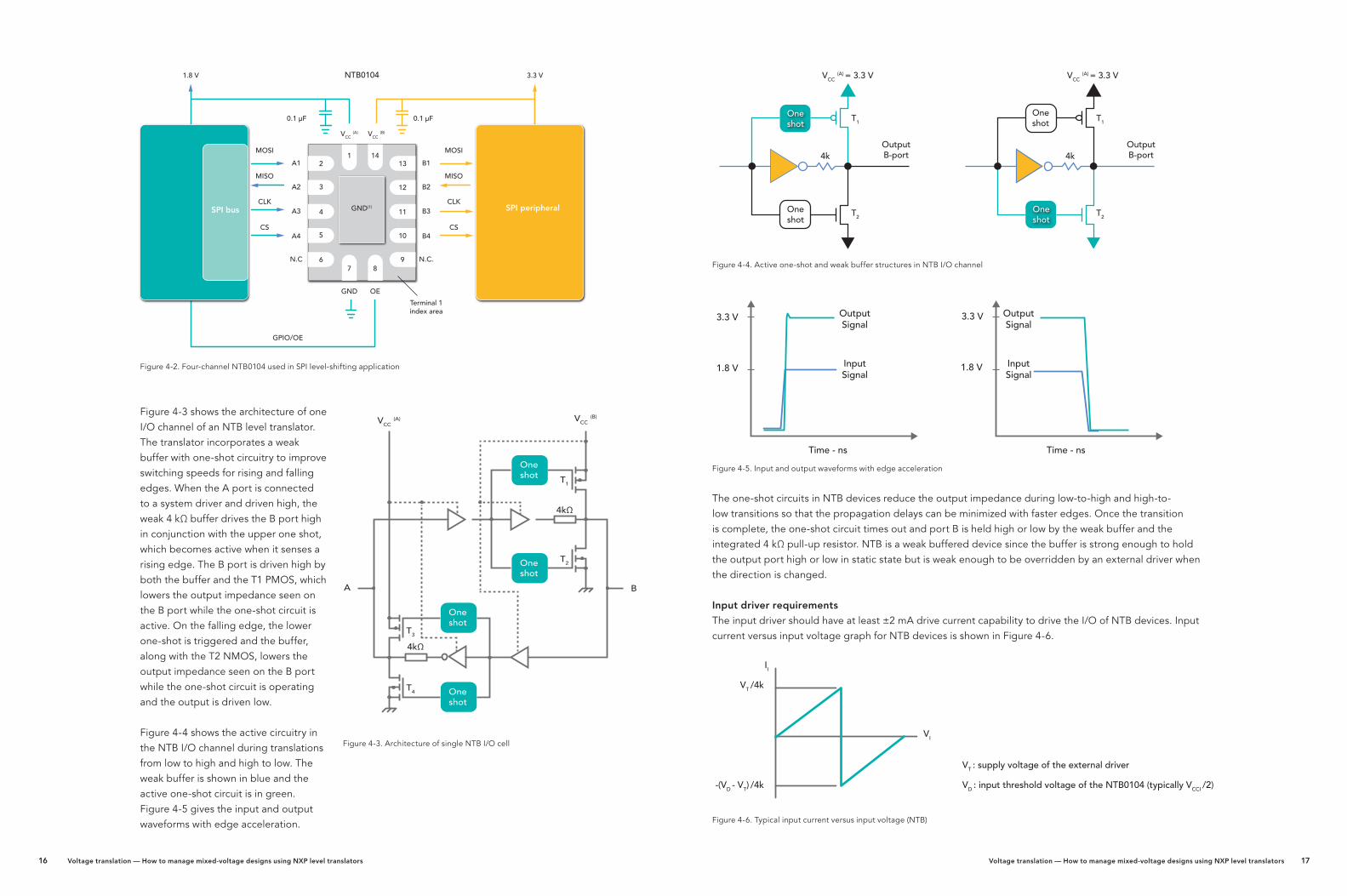
Figure 4-2. Four-channel NTB0104 used in SPI level-shifting application
Figure 4-3 shows the architecture of one I/O channel of an NTB level translator. The translator incorporates a weak buffer with one-shot circuitry to improve switching speeds for rising and falling edges. When the A port is connected to a system driver and driven high, the weak 4 kΩ buffer drives the B port high in conjunction with the upper one shot, which becomes active when it senses a rising edge. The B port is driven high by both the buffer and the T1 PMOS, which lowers the output impedance seen on the B port while the one-shot circuit is active. On the falling edge, the lower one-shot is triggered and the buffer, along with the T2 NMOS, lowers the output impedance seen on the B port while the one-shot circuit is operating and the output is driven low.
Figure 4-4 shows the active circuitry in the NTB I/O channel during translations from low to high and high to low. The weak buffer is shown in blue and the active one-shot circuit is in green. Figure 4-5 gives the input and output waveforms with edge acceleration.
Figure 4-4. Active one-shot and weak buffer structures in NTB I/O channel
Figure 4-5. Input and output waveforms with edge acceleration
The one-shot circuits in NTB devices reduce the output impedance during low-to-high and high-to-low transitions so that the propagation delays can be minimized with faster edges. Once the transition is complete, the one-shot circuit times out and port B is held high or low by the weak buffer and the integrated 4 kΩ pull-up resistor. NTB is a weak buffered device since the buffer is strong enough to hold the output port high or low in static state but is weak enough to be overridden by an external driver when the direction is changed.
Input driver requirements
The input driver should have at least ±2 mA drive current capability to drive the I/O of NTB devices. Input current versus input voltage graph for NTB devices is shown in Figure 4-6.
Figure 4-6. Typical input current versus input voltage (NTB)
SPI peripheralSPI bus GND(1)
GPIO/OE
Terminal 1index area
CS
CLK
MISO
MOSI
0.1 µF 0.1 µF
1.8 V NTB0104 3.3 V
CS
CLK
MISO
MOSI1 14
7 8
13
12
11
10
9
2A1
A2
A3
A4
N.C
GND OE
VCC (A) VCC (B)
B1
B2
B3
B4
N.C.
3
4
5
6
T1
T2
4k
VCC (A) = 3.3 V
Oneshot
OutputB-port
Oneshot
T1
T2
4k
VCC (A) = 3.3 V
Oneshot
OutputB-port
Oneshot
OutputSignal
InputSignal
OutputSignal
InputSignal
Time - ns Time - ns
1.8 V
3.3 V
1.8 V
3.3 V
II
VI
VT /4k
VT : supply voltage of the external driver
VD : input threshold voltage of the NTB0104 (typically VCCI /2)-(VD - VT) /4k
VCC (A)
A B
T1
T2
T3
T4
4kΩ
4kΩ
VCC (B)
Oneshot
Oneshot
Oneshot
Oneshot
Figure 4-3. Architecture of single NTB I/O cell
18 Voltage translation — How to manage mixed-voltage designs using NXP level translators Voltage translation — How to manage mixed-voltage designs using NXP level translators 19
Since NTB buffers are designed for driving high-impedance loads, it is important to carefully select the external pull-up or pull-down resistors if they are used in the application. For any external pull-up or pull-down resistor used with the NTB resistor, a resistor divider network is formed with a 4 kΩ buffer. The value of the external resistor should be large enough (typically greater than 50 kΩ) so that there is little change on VOH or VOL levels.
For example, the value of VOL can be determined from the following equation, when a 50 kΩ external pull-up is used:
VOL = 4k/50k + 4k x VCCO = 0.075 x VCCO
During output transitions, the typical output impedance is 70 Ω at VCCO equals 1.2 to 1.8 V, 50 Ω at VCCO equals 1.8 to 3.3 V and 40 Ω at VCCO equals 3.3 to 5.0 V. When the circuits are active, a resulting high AC drive is realized by turning on T1 and the rising-edge speeds up. The output port is maintained at a high signal level through this 4 kΩ internal resistor. During low-to-high transitions, one-shot circuits turn on the PMOS transistors T1 for a short time, accelerating the output edges. However, the one-shot circuits are turned off when output voltage reaches approximately 95% of the steady-state value. For high-to-low output transitions, the one-shot turns off when output voltage reaches approximately 5% of the steady-state value.
Output-enable (OE) control
NTB level translators offer a maximum power consumption of 5 µA when OE is high. When the OE is low, the NTB translator buffer will be disabled and the outputs are put into high impedance for increased power savings. The /OE pin is referenced to VCC(A) voltage supply and when outputs are disabled, the one-shot and 4 kΩ buffer are also disabled for both the A and B ports. In this state, output leakage IOZ will be less than ±2 µA. If the application does not require output-enable control, the OE pin should be tied to VCC(A) supply and must never be left floating. A floating OE results in excessive quiescent current consumed by the device, which increases the total power consumption. Unwanted output oscillations may also result due to indeterminate logic level at /OE pin.
The outputs of NTB devices are tri-stated in case any of the two power supplies is 0 V. This feature, called VCC isolation, means that if VCC(B) or VCC(A) equals 0 V, the I/O of A and B ports are in high impedance. These devices are fully specified for partial power-down applications using IOFF. The IOFF circuitry disables the output, preventing the presence of damaging backflow current when the device is powered down.
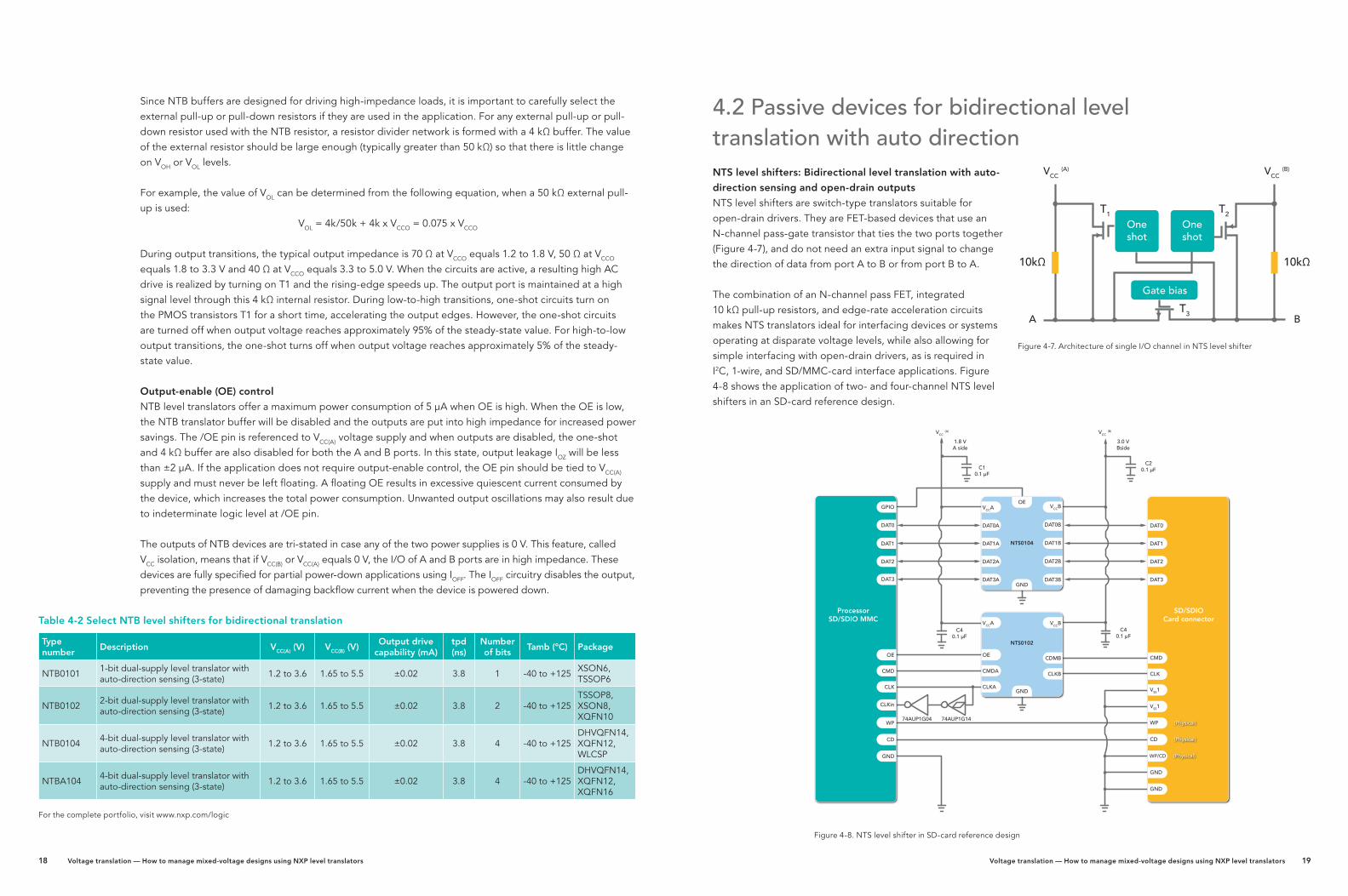
4.2 Passive devices for bidirectional level translation with auto directionNTS level shifters: Bidirectional level translation with auto-
direction sensing and open-drain outputs
NTS level shifters are switch-type translators suitable for open-drain drivers. They are FET-based devices that use an N-channel pass-gate transistor that ties the two ports together (Figure 4-7), and do not need an extra input signal to change the direction of data from port A to B or from port B to A.
The combination of an N-channel pass FET, integrated 10 kΩ pull-up resistors, and edge-rate acceleration circuits makes NTS translators ideal for interfacing devices or systems operating at disparate voltage levels, while also allowing for simple interfacing with open-drain drivers, as is required in I2C, 1-wire, and SD/MMC-card interface applications. Figure 4-8 shows the application of two- and four-channel NTS level shifters in an SD-card reference design.
Figure 4-8. NTS level shifter in SD-card reference design
Type number
Description VCC(A) (V) VCC(B) (V)Output drive
capability (mA)tpd (ns)
Number of bits
Tamb (°C) Package
NTB0101 1-bit dual-supply level translator with auto-direction sensing (3-state) 1.2 to 3.6 1.65 to 5.5 ±0.02 3.8 1 -40 to +125 XSON6,
TSSOP6
NTB0102 2-bit dual-supply level translator with auto-direction sensing (3-state) 1.2 to 3.6 1.65 to 5.5 ±0.02 3.8 2 -40 to +125
TSSOP8, XSON8, XQFN10
NTB0104 4-bit dual-supply level translator with auto-direction sensing (3-state) 1.2 to 3.6 1.65 to 5.5 ±0.02 3.8 4 -40 to +125
DHVQFN14, XQFN12, WLCSP
NTBA104 4-bit dual-supply level translator with auto-direction sensing (3-state) 1.2 to 3.6 1.65 to 5.5 ±0.02 3.8 4 -40 to +125
DHVQFN14, XQFN12, XQFN16
For the complete portfolio, visit www.nxp.com/logic
Table 4-2 Select NTB level shifters for bidirectional translation
VCC (A)
A B
T1 T2
T3
10kΩ 10kΩ
VCC (B)
Oneshot
Gate bias
Oneshot
Figure 4-7. Architecture of single I/O channel in NTS level shifter
1.8 VA side
3.0 VBside
VCC (A) VCC (B)
C40.1 µF
C10.1 µF
C20.1 µF
C40.1 µF
DAT0
DAT1
GPIO
DAT2
DAT3
OE
CMD
CLK
CLKin
WP
CD
GND
VCCA
DAT0A
DAT1A
DAT2A
DAT3A
VCCA
OE
CMDA
CLKA
VCCB
DAT0B
DAT1B
DAT2B
DAT3B
VCCB
CDMB
CLKB
OE
GND
GND
DAT0
DAT1
DAT2
DAT3
CMD
CLK
VSS1
VSS1
WP
CD
WP/CD
GND
GND
(Physical)
(Physical)
(Physical)
NTS0104
NTS0102
74AUP1G1474AUP1G04
ProcessorSD/SDIO MMC
SD/SDIOCard connector
20 Voltage translation — How to manage mixed-voltage designs using NXP level translators Voltage translation — How to manage mixed-voltage designs using NXP level translators 21
The N-channel pass-gate transistor is used to open and close the connection between the A and B ports. When a driver connected to A or B port is low, the opposite port is, in turn, pulled low by the N2 pass-gate transistor. The gate bias voltage of the pass-gate transistor (T3) is set at approximately one threshold voltage above the VCC level of the low-voltage side.
During a low-to-high transition, the output one-shot accelerates the output transition by switching on the PMOS transistors (T1, T2), bypassing the 10 kΩ pull-up resistors, and increasing current drive capability. The one-shot is activated once the input transition reaches approximately VCCI/2, and is de-activated approximately 50 ns after the output reaches VCCO/2. During the acceleration time, the driver output resistance is between approximately 50 and 70 Ω. To avoid signal contention and minimize dynamic ICC, the user should wait for the one-shot circuit to turn off before applying a signal in the opposite direction.
The pass-gate transistor T3 is on when VGS is greater than VT. When one side of T3 is held low by an external driver, with the input to T3 at 0 V, T3 will be on and the output of T3 will be held to nearly 0 V due to the on-state resistance of T3. As the input voltage rises due to a rising edge, the output voltage of T3 tracks the input until the input voltage reaches VGATE minus VT and T3 turns off. After T3 stops conducting, the input and output ports continue to rise to their respective supply voltages due to the internal pull-up resistors. In the second case, both ports start with high levels since the integrated pull-up resistors tie the inputs to the respective supply voltages, VCC(A) and VCC(B). When the input ports are pulled low by external drivers, T3 starts to conduct when VGS is greater than VT and output starts tracking the input. The source current needed for this operation must be provided by the external driver connected to the A or B port.
To achieve faster data rates through the device, NTS translators include rising edge-rate acceleration circuitry to provide stronger AC-drive by bypassing the integrated 10 kΩ pull-up resistors through a low-impedance path during low-to-high signal transitions. A one-shot circuit with associated T1/T2 PMOS transistors is used to increase switching speeds for the rising-edge input signals. When a rising edge is detected by the one-shot circuit, the T1/T2 PMOS transistors turn on momentarily to rapidly drive the port high, effectively lowering the output impedance seen on that port and speeding up the rising-edge inputs.
Input driver requirements
Since NTS level shifters are switch-type level shifters, properties of the input driver directly affect the output signal. The external open-drain or push-pull driver applied to an I/O determines the static current sinking capability of the system; the maximum data rate high-to-low output transition time (tTHL) and the propagation delay (tPHL) depend on the output impedance and the edge rate of the external driver. The limits provided in the datasheet for these parameters assume use of a driver with output impedance below 50 Ω.
Output load considerations
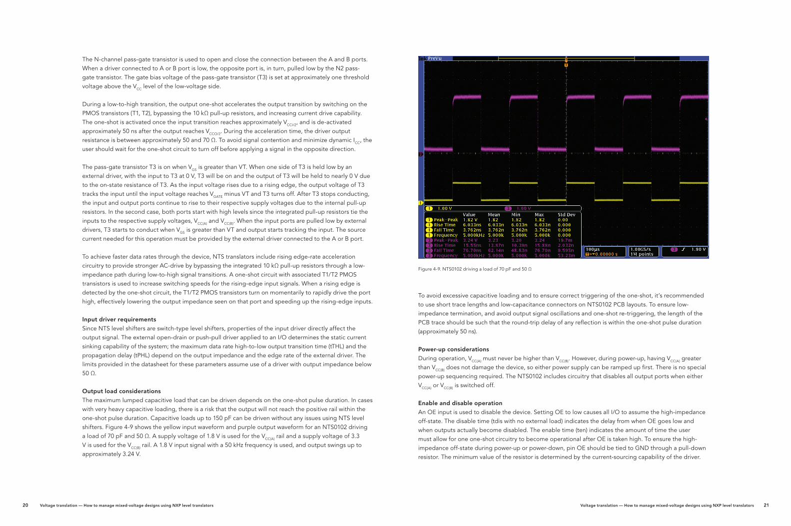
The maximum lumped capacitive load that can be driven depends on the one-shot pulse duration. In cases with very heavy capacitive loading, there is a risk that the output will not reach the positive rail within the one-shot pulse duration. Capacitive loads up to 150 pF can be driven without any issues using NTS level shifters. Figure 4-9 shows the yellow input waveform and purple output waveform for an NTS0102 driving a load of 70 pF and 50 Ω. A supply voltage of 1.8 V is used for the VCC(A) rail and a supply voltage of 3.3 V is used for the VCC(B) rail. A 1.8 V input signal with a 50 kHz frequency is used, and output swings up to approximately 3.24 V.
Figure 4-9. NTS0102 driving a load of 70 pF and 50 Ω
To avoid excessive capacitive loading and to ensure correct triggering of the one-shot, it’s recommended to use short trace lengths and low-capacitance connectors on NTS0102 PCB layouts. To ensure low-impedance termination, and avoid output signal oscillations and one-shot re-triggering, the length of the PCB trace should be such that the round-trip delay of any reflection is within the one-shot pulse duration (approximately 50 ns).
Power-up considerations
During operation, VCC(A) must never be higher than VCC(B). However, during power-up, having VCC(A) greater than VCC(B) does not damage the device, so either power supply can be ramped up first. There is no special power-up sequencing required. The NTS0102 includes circuitry that disables all output ports when either VCC(A) or VCC(B) is switched off.
Enable and disable operation
An OE input is used to disable the device. Setting OE to low causes all I/O to assume the high-impedance off-state. The disable time (tdis with no external load) indicates the delay from when OE goes low and when outputs actually become disabled. The enable time (ten) indicates the amount of time the user must allow for one one-shot circuitry to become operational after OE is taken high. To ensure the high-impedance off-state during power-up or power-down, pin OE should be tied to GND through a pull-down resistor. The minimum value of the resistor is determined by the current-sourcing capability of the driver.

22 Voltage translation — How to manage mixed-voltage designs using NXP level translators Voltage translation — How to manage mixed-voltage designs using NXP level translators 23
Pull-up or pull-down resistors on I/O lines
Each A port I/O has an internal 10 kΩ pull-up resistor to VCC(A), and each B port I/O has an internal 10 kΩ pull-up resistor to VCC(B). If a smaller value of pull-up resistor is required, an external resistor must be added parallel to the internal 10 kΩ. This will affect the VOL level. When OE goes low the internal pull-ups of the NTS0102 are disabled.
NTSX level shifters: Bidirectional level translation
with auto-direction sensing, open-drain outputs,
and dual-edge accelerators
NTSX level shifters are similar to NTS devices but use a modified architecture that enables use at higher capacitive loads (typically up to 600 pF). Figure 4-10 gives the architecture of a single NTSX I/O channel.
There are two N-channel pass-gate transistors that tie the ports together. There is an output edge-rate accelerator that detects and accelerates rising and falling edges on the I/O pins (Figure 4-11).
During an input transition, a one-shot accelerates the output transition by switching on the PMOS transistors (T1, T3) for a low-to-high transition. Alternatively, the one-shot switches on the NMOS transistors (T2, T4) for a high-to-low transition (Figure 4-12). Once activated, the one-shot is deactivated after approximately 25 ns. During the acceleration time, the driver output resistance is between approximately 10 and 35 Ω. To avoid signal contention, the application must not exceed the maximum data rate or must wait for the one-shot circuit to turn off before applying a signal in the opposite direction.
Input driver requirements
Because the NTSX2102 is a switch-type translator, properties of the input driver directly affect the output signal. The external open-drain driver applied to an I/O determines the static current sinking capability of the system. The maximum data rate, output transition times (tTHL, tTLH), and propagation delays (tPHL, tPLH) depend on the output impedance and the edge-rate of the external driver.
Output load considerations
The maximum lumped capacitive load that can be driven depends on the one-shot pulse duration and has been tuned to 600 pF. In cases with higher capacitive loading, there is a risk that the output does not reach the positive rail within the one-shot pulse duration. To avoid excessive capacitive loading and ensure correct triggering of the one-shot, use short trace lengths and low-capacitance connectors on NTSX2102 PCB layouts. The length of the PCB trace should be such that the round-trip delay of any reflection is within the one-shot pulse duration. Such a length ensures low impedance termination and avoids output signal oscillations and one-shot retriggering.
Output enable (OE)
An OE input is used to disable the device. Setting OE to low causes all I/O to assume the high-impedance off-state. One of the advantages of NTSX translators is that either VCC(A) or VCC(B) can be powered up first. Defining the OE pin reduces dissipation during power-up. The OE pin can be connected via a pull-down resistor to GND or, if the application allows, hardwired to VCC(A). If the OE pin is hardwired to VCC(A), either supply can be powered up or down first. If a pull-down is used, the following sequences are recommended.
Table 4-3 Select NTS and NTSX level shifters for bidirectional translation
NVT level shifters: Bidirectional level translation with auto-direction sensing, open-drain outputs,
no external pull-ups
NVT level shifters perform bidirectional translation using an array of matching N-channel pass transistors with their gates tied together internally at the enable (EN) pin (Figure 4-13).
A B
T1
T2
T5 T6
T3
T4
VCC (A)
VCC (A)
VCC (B)
VCC (B)
Oneshot
Oneshot
Oneshot
Oneshot
Figure 4-10. Architecture of NTSX2102 I/O channel
4
3
2
1
0
VI (An) (V)
VO (Bn) (V)
T (ns)
4
3
2
1
00
20 40 60 80 100
Figure 4-11. Input and output waveforms showing edge-rate acceleration
One shottime (ns)
80
60
40
20
0
1 2 3 4 5
V (V)
6
Figure 4-12. One-shot pulse time versus VCCO
Type number
Description VCC(A) (V) VCC(B) (V)Output drive
capability (mA)tpd (ns)
Number of bits
Tamb (°C) Package
NTS0101 1-bit dual-supply level translator with auto-direction sensing (3-state) 1.65 to 3.6 2.3 to 5.5 -0.02 4.4 1 -40 to +125 XSON6,
TSSOP6
NTS0102 2-bit dual-supply level translator with auto-direction sensing (3-state) 1.65 to 3.6 2.3 to 5.5 -0.02 4.4 2 -40 to +125
TSSOP8, XSON8, XQFN8, XQFN10
NTS0103 3-bit dual-supply level translator with auto-direction sensing (3-state) 1.65 to 3.6 2.3 to 5.5 -0.02 4.4 2 -40 to +125 XQFN10
NTS0104 4-bit dual-supply level translator with auto-direction sensing (3-state) 1.65 to 3.6 2.3 to 5.5 -0.02 4.4 4 -40 to +125
DHVQFN14, XQFN12, TSSOP14, WLCSP
NTSX2101 2-bit dual-supply level translator with auto-direction sensing (3-state) 1.65 to 5.5 1.65 to 5.5 6 2 2 -40 to +125 XSON8,
XQFN8
For the complete portfolio, visit www.nxp.com/logic
For power-up
1. Apply power to either supply pin 2. Apply power to the other supply pin 3. Enable the device by driving OE high
For power-down
1. Disable the device by driving OE low 2. Remove power from either supply pin 3. Remove power from the other supply pin

24 Voltage translation — How to manage mixed-voltage designs using NXP level translators Voltage translation — How to manage mixed-voltage designs using NXP level translators 25
Figure 4-13. Typical NVT20xx device schematic
A similar method, but with different characteristics for RON, CIO, and ESD protection, is used by two other level translators – the PCA9306, a 2-bit dual-supply level translator with auto-direction sensing (which is the same as the NVT2002 but with support for the SMBus and a wider range of packages), and the GTL2005, a 4-bit GTL-to-LVTTL bidirectional non-latched translator (see section 3).
Basic operation
One of the Field-Effect Transistors (FETs) is used as a reference transistor, and the remainder as pass transistors. The low side (A1 to An) is the FET source, while the high side (B1 to Bn) is the FET drain. On the low side, the voltage of the reference transistor is the limit for the remaining pass transistors. The gate of the reference transistor should be tied to its drain to ensure that the FETs operate within the saturation region.
The reference transistor and one resistor are used to set VBIAS and the gate voltage (VG) for all the pass transistors. The gate voltage is VCC(A) plus the gate-to-source voltage (VGS). VGS can vary from 0.6 to 1.0 V. The pass transistors on the low side are limited to VCC(A).
When either an An or Bn port is driven low, the FET is turned on and a low-resistance path exists between the An and Bn port. The low on-state resistance (RON) of the pass transistor allows connections to be made with minimal propagation delay.
When the Bn port is driven or pulled high, the voltage on the An port is limited to VCC(A). When the An port is driven or pulled high, the Bn port is pulled to VCC(B) by the pull-up resistors. VCC(A) is set equal to the I/O voltage level of the CPU and VCC(B) is set equal to the I/O voltage level of the peripheral device. This enables seamless translation between high and low levels without the need for directional control.
When EN is connected through a 200 kΩ pull-up resistor to a high-voltage VCC(B), and the An and Bn I/O are connected, the translator switch is on, allowing bidirectional data flow between ports. When EN is pulled low, the transistor switch is off and a high-impedance or disconnect state exists between ports. In this way, these translators protect new, lower-voltage devices from the overvoltage and ESD conditions applied by older, high-voltage devices, and make easy work of translating the VIH and VOH switching levels.
Bidirectional level translation with open-drain I/O
For bidirectional level translation, the drivers on both sides of the translator either must be open-drain outputs or must be controlled to prevent contention between a high level on an output driver on one side and a low level on the other.
Using an open-drain device means there has to be pull-up resistors on the B side, and the resistors have to be sized so as not to overload the output drivers.
With the NVT20xx and PCA9306, if VCC(B) minus VCC(A) is greater than 1 V, then pull-up resistors are not required on the A side. If, however, VCC(B) minus VCC(A) is less than 1 V, then pull-up resistors must be used on the A side to bring the An outputs to VCC(A). Note that if pull-up resistors are required on both the A and B sides, then the equivalent pull-up resistor value becomes the parallel combination of the two resistors when the pass transistor is on.
A similar situation exists with the GTL2000, GTL2002, GTL2003, and GTL2010. If VCC(B) minus VCC(A) is greater than or equal to 1.5 V, then pull-up resistors are not required on the A/S side. If, however, the difference is less than 1.5 V, then pull-up resistors must be used on both the A/S and B/D sides, and the equivalent pull-up resistor value becomes the parallel combination of the two resistors when the pass transistor is on.
Unidirectional level translation and push-pull I/O
The translators support unidirectional level translation (low to high or high to low) with push-pull or totem-pole I/O, but the I/O must be the only driver on the bus during translation. Using this configuration for bidirectional push-pull control requires a direction control bit to determine which I/O is acting on the bus and prevent bus contention. Details for unidirectional translation are given in application note AN11127.
VCC (B) = 3.3 V
VCC (A) = 1.2 V
NVT20xx
200 k
1 k
0.1 µF
1 k 1 k 1 k
EN
VREFB
Open-drainperipheral
high-voltageI/O bus
Open-drainGPU low-voltage
I/O bus
VREFA
GND
PasstransistorsReference
transistors
(drain)
(source)
(gate)
A1 A2 A3
B1 B2 B3 BN
AN

26 Voltage translation — How to manage mixed-voltage designs using NXP level translators Voltage translation — How to manage mixed-voltage designs using NXP level translators 27
CBTD and CBTLVD bus switches: Devices that perform signal switching and level translation
In designs that require voltage translation and signal switching, a crossbar switch equipped with a diode can be used. Bus switches are natural translators. The switch function turns the signal on or off and, as a result, the output voltage, also called the pass voltage (VPASS), is lower than the VCC. A bus switch placed between a 5 V memory and a 3 V CPU, for example, can perform double duty, providing signal switching as well as level translation (Figure 4-14). There is no capacitive isolation between inputs and outputs when the switches are off. The drive capability of bus switches depends on the load connected and the output drive of the driver.
The NXP CBT product family includes a number of bus switches. The CBTD series adds a diode to the lower gate voltage and, as a result, typically has a VPASS that is 1 V lower than the CBT series. This makes the CBTD series a good choice for applications that need switching between 3 V devices and/or translation from 5.0 to 3.3 V.
Figure 4-15 gives results from a CBTD3306, a dual bus switch with level shifting. Assuming a switch current of 6 mA and an operating temperature of 25 °C, when VCC is 5 V, the output/pass voltage would approximately 2.7 V. Note that the voltage at switch input (VIN) is higher than VPASS and could be up to 7 V. Under the same conditions, but with a smaller switch current, such as 100 µA, VPASS would be closer to 3 V.
The CBTD3306 can also be used for 3 V signal switching when VCC is in the range of 4.5 to 5.5 V. For example, assuming a typical RON of 17 Ω and a switch current of 15 mA, when VCC is 4.5 V, and the input voltage is 2.4 V, the switch output will be 2.145 V. CBTD data sheets provide further details.
CBTLVD devices are low-voltage variants of the CBTD series. They are suitable for translating signals from 3.3 to 1.8 V. Figure 4-16 gives results from a CBTLVD3244, an 8-bit level-shifting bus switch with 4-bit output enables, when the input voltage is greater than VPASS, up to 4.6 V.
Type number Description VCC(A) (V) VCC(B) (V)Number of bits
Package
NVT2001 1-bit dual-supply level translator with auto-direction sensing 1.0 to 3.6 1.0 to 5.5 1
TSSOP8, XSON8U, XSON6
NVT2002* 2-bit dual-supply level translator with auto-direction sensing 1.0 to 3.6 1.8 to 5.5 2
TSSOP8, XSON8, XQFN10, XQFN8
NVT2003 3-bit dual-supply level translator with auto-direction sensing 1.0 to 3.6 1.8 to 5.5 3 TSSOP10
NVT2004 4-bit dual-supply level translator with auto-direction sensing 1.0 to 3.6 1.8 to 5.5 4 HXSON12
NVT2006 6-bit dual-supply level translator with auto-direction sensing 1.0 to 3.6 1.8 to 5.5 6
DHVQFN16, HVQFN16, TSSOP16
NVT2008 8-bit dual-supply level translator with auto-direction sensing 1.0 to 3.6 1.8 to 5.5 8 DHVQFN20,
TSSOP20
NVT2010 10-bit dual-supply level translator with auto-direction sensing 1.0 to 3.6 1.8 to 5.5 10
DHVQFN24, HVQFN24, TSSOP24
* The PCA9306 is the same as the NVT2002 but with more package options (SO8, VSSOP8)For the complete portfolio, visit nxp.com/logic
Table 4-4. Select NVT bidirectional translators
VCC = 5 V CBTD3384
CBT3384
OE
3 V
3 V CPU
3 V MEMORY
5 V CPU
5 V I/O5 V
3 V 5 V
2.0
2.0
2.0
(1)
(2)
(3)
(4)
2.0
2.0
Vpass (V)
5.24.4 4.8 5.6VCC (V)
3.0 3.2 3.4
20 µA
2 mA
4 mA
100 µA
3.6
1.90
Vpass (V)
VCC (V)
1.85
1.80
1.75
1.70
1.65
1.60
1.55
Figure 4-15. CBTD pass voltage versus supply voltage
Figure 4-14. Sample application with CPU and memory
Figure 4-16. CBTLVD pass voltage versus supply voltage
Type number Description VCC (V)VPASS (V)
Logic switching
levelsRON (Ω)
f(-3dB) (MHz)
tpd (ns)
Tamb (°C) Package
CBTD16210 20-bit bus-switch level translator 4.5 to 5.5 3.3 TTL 7 300 0.25 -40 to +85 TSSOP48, SSOP48
CBTD16211 24-bit bus-switch level translator 4.5 to 5.5 3.3 TTL 7 300 0.25 -40 to +85 TSSOP56, SSOP56
CBTD3306 Dual bus-switch level translator 4.5 to 5.5 3.3 TTL 7 300 0.25 -40 to +85SO8, XQFN8U, XSON8, TSSOP8
CBTD3384 10-bit bus-switch level translator 4.5 to 5.5 3.3 TTL 7 300 0.25 -40 to +85 SO24, SSOP24, TSSOP24
CBTD3861 10-bit bus-switch level translator 4.5 to 5.5 3.3 TTL 7 300 0.25 -40 to +85DHVQFN24, SSOP24, TSSOP24
CBTLVD3244 Octal bus switch level translator 3.0 to 3.6 1.8 CMOS / LVTTL 7 400 0.2 -40 to +125
DHVQFN20, SSOP20, TSSOP20
CBTLVD3245 Octal bus-switch level translator 3.0 to 3.6 1.8 CMOS / LVTTL 7 400 0.2 -40 to +125
DHVQFN20, SSOP20, TSSOP20
CBTLVD3384 10-bit bus-switch level translator 3.0 to 3.6 1.8 CMOS / LVTTL 7 400 0.2 -40 to +125
DHVQFN24, SSOP24, TSSOP24
CBTLVD3861 10-bit bus-switch level translator 3.0 to 3.6 1.8 CMOS / LVTTL 7 400 0.2 -40 to +125
DHVQFN24, SSOP24, TSSOP24
For the complete portfolio, visit nxp.com/logic
Table 4-5. Select CBTD and CBTLVD bus switches for voltage translation
28 Voltage translation — How to manage mixed-voltage designs using NXP level translators Voltage translation — How to manage mixed-voltage designs using NXP level translators 29
This section discusses level translators that make it easier to work with SIM cards and special translators for the I2C-bus.
5.1 Translators for use with SIM cardsNVT4555 WLCSP bidirectional SIM card interface level translator and supply voltage LDO
The NVT455 interfaces between the host processor of a smartphone and its SIM card (Figure 5-1). Available in a tiny wafer-level chipscale package (WLCSP), it combines robust performance with the smallest available footprint. The device complies with the SIM power supply, includes EMI and ESD protection, and handles the shutdown sequence specified by the ISO 7816-3 specification.
Figure 5-1. NVT4555 interfacing with a typical SIM card
The internal low-dropout (LDO) regulator supplies power to the SIM card using a high power supply rejection ratio (PSSR) at a very low dropout voltage (VBAT-VSIM). The NVT455 provides two levels of fixed voltage regulation, at 1.8 or 2.95 V, selectable using the CTRL pin.
Using the ISO 7816-3 shutdown sequence for the SIM card signals ensures the card is properly disabled and, during hot swap, the shutdown sequence helps avoid data corruption and improper writes.
The NVT4555 has greater than ± 8 kV contact IEC 61000-4-2 ESD protection for the SIM pins and standard ± 2 kV contact for all other pins.
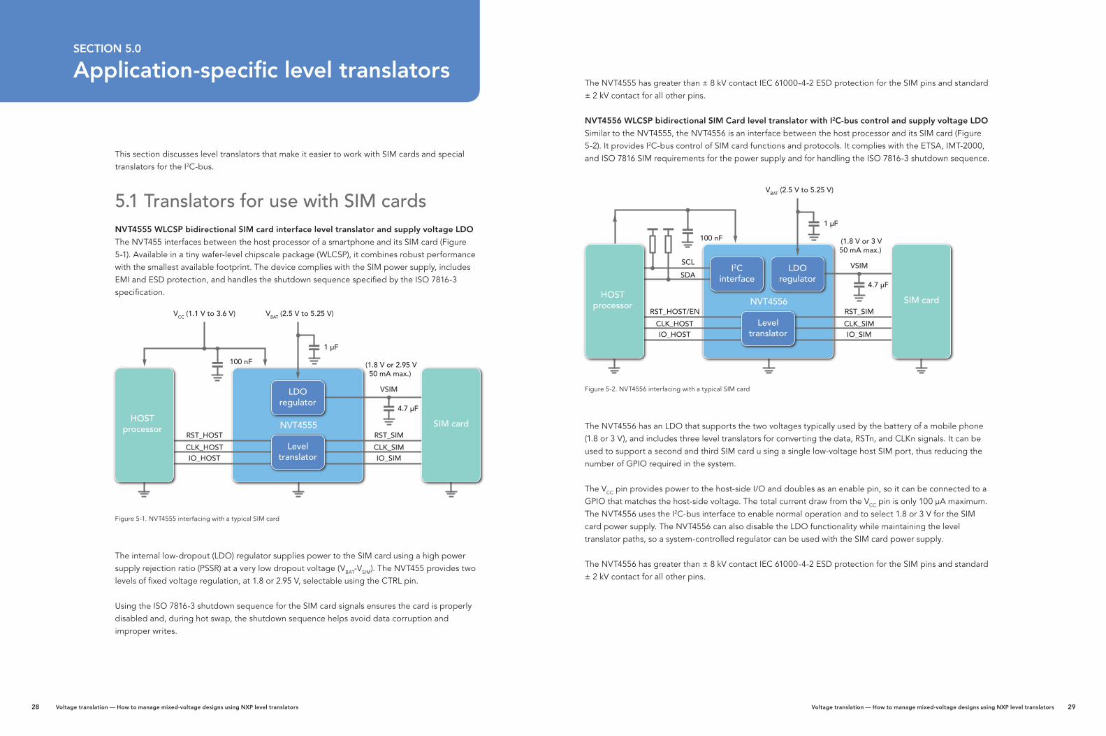
NVT4556 WLCSP bidirectional SIM Card level translator with I2C-bus control and supply voltage LDO
Similar to the NVT4555, the NVT4556 is an interface between the host processor and its SIM card (Figure 5-2). It provides I2C-bus control of SIM card functions and protocols. It complies with the ETSA, IMT-2000, and ISO 7816 SIM requirements for the power supply and for handling the ISO 7816-3 shutdown sequence.
Figure 5-2. NVT4556 interfacing with a typical SIM card
The NVT4556 has an LDO that supports the two voltages typically used by the battery of a mobile phone (1.8 or 3 V), and includes three level translators for converting the data, RSTn, and CLKn signals. It can be used to support a second and third SIM card u sing a single low-voltage host SIM port, thus reducing the number of GPIO required in the system.
The VCC pin provides power to the host-side I/O and doubles as an enable pin, so it can be connected to a GPIO that matches the host-side voltage. The total current draw from the VCC pin is only 100 μA maximum. The NVT4556 uses the I2C-bus interface to enable normal operation and to select 1.8 or 3 V for the SIM card power supply. The NVT4556 can also disable the LDO functionality while maintaining the level translator paths, so a system-controlled regulator can be used with the SIM card power supply.
The NVT4556 has greater than ± 8 kV contact IEC 61000-4-2 ESD protection for the SIM pins and standard ± 2 kV contact for all other pins.
Application-specific level translatorsSECTION 5.0
NVT4555
VCC (1.1 V to 3.6 V)
100 nF
1 μF
VSIM
4.7 μF
RST_HOST
CLK_HOSTIO_HOST
RST_SIM
CLK_SIMIO_SIM
Leveltranslator
SIM cardNVT4555HOST
processor
LDOregulator
VBAT (2.5 V to 5.25 V)
(1.8 V or 2.95 V50 mA max.)
NVT4555
100 nF
1 μF
VSIM
4.7 μF
RST_HOST/EN
CLK_HOST
SDA
SCL
IO_HOST
RST_SIM
CLK_SIMIO_SIM
Leveltranslator
SIM cardNVT4556HOST
processor
LDOregulator
I2Cinterface
VBAT (2.5 V to 5.25 V)
(1.8 V or 3 V50 mA max.)

30 Voltage translation — How to manage mixed-voltage designs using NXP level translators Voltage translation — How to manage mixed-voltage designs using NXP level translators 31
5.2 I2C muxes and switches that also perform bidirectional translationPCA954x bidirectional translating muxes and switches
Some specialized devices only have one I2C or SMBus address. When several identical devices are needed in the same system, devices can’t be accessed individually. Multiplexers and switches split the I2C-bus into several branches and allow the I2C master to select and address one of multiple identical devices without address conflicts.
Many I2C peripheral devices operate at different voltage levels due to the analog nature of the sensors. This would normally require a separate master for each different power supply. Multiplexers and switches permit a single master to interface with multiple peripheral devices that use different power supply voltages.
The PCA954x are I2C multiplexers and switches that also perform bidirectional translation (Figure 5-3).
Figure 5-3. Sample application using a PCA954x mux/switch
Figure 5-4. PCA9540B block diagram
The PCA9540B (Figure 5-4) serves as an example for the entire family.
The upstream SCL/SDA pair fans out to downstream pairs or channels controlled by FET switches. The number of downstream pairs depends on the device. The I2C signals on the upstream channel are passed on to all the downstream channels, without amplification. The I2C-bus limit of 400 pF must be observed for the upstream channel and for all active downstream channels. Pull-up resistors are required on all upstream and downstream channels.
I2C commands from the bus master on the upstream channel or any active downstream channel can turn any channel on or off. The channel status is changed when the stop command is sent. A multiplexer allows only a single downstream channel to be selected at any time, but a switch allows any or all downstream channels to be connected. Since there is direct connection between the upstream and downstream buses, the pull-up resistors on all connected buses are paralleled and there is added capacitance on all connected buses.
With a MOSFET pass transistor placed between the upstream and downstream buses, any excursions of the bus voltage on the downstream side are limited by the gate voltage applied to the pass transistors. The downstream bus can only rise to the gate voltage minus the transistor’s threshold voltage. Using the pass transistor’s gate voltage as its power supply lets the PCA954x perform voltage-level translation.
The graph in figure 5-5 shows that the I2C voltage can be translated between the various channels of a PCA954x device.
Master
5 V 5 V
5 V 5 V
3.3 V 3.3 V
MUX orswitch
PCA954x
Slave
Slave
SC1
Switch control logic
Power-onreset
Inputfilter
I2C-buscontrol
VSS
VDD
SCL
SDA
SC0
SD1
SD0

32 Voltage translation — How to manage mixed-voltage designs using NXP level translators
Figure 5-5. PCA954x voltage translation
For example, assume the upstream channel uses 5 V while the downstream channel uses 3.3 V. If the PCA954x is supplied with 3.3 V, it will clamp the voltage to about 2.3 V so the 5 V will not appear on the 3.3 V side. A pull-up resistor on the 3.3 V side then pulls it all the way up to the 3.3 V rail. In most situations, the design engineer should use the maximum voltage curve since this is the situation found over the entire temperature range. The important thing to note is that the multiplexer/switch should be supplied with the lowest I2C voltage needed to ensure proper level translation.
Table 5-1. Select PCA954x I2C muxes and switches
VDD
VO (SW)
(V)
5.54.53.0 4.0
3.0
2.0
4.0
5.0
(V)
1.03.5 5.02.52.0
Maximum
Typical
Minimum
Type number FunctionNumber of addresses
Hardware reset
Voltage range (V)
PCA9540B 1:2 mux 1 No 2.3 to 5.5
PCA9541 2:1 mux, master selector 16 Yes 2.3 to 5.5
PCA9542A 1:2 mux 8 No 2.3 to 5.5
PCA9543A 1:2 switch 4 Yes 2.3 to 5.5
PCA9544A 1:4 mux 8 No 2.3 to 5.5
PCA9545 1:4 switch 4 Yes 2.3 to 5.5
PCA9546A 1:4 switch 8 Yes 2.3 to 5.5
PCA9547 1:8 mux 8 Yes 2.3 to 5.5
PCA9548A 1:8 switch 8 Yes 2.3 to 5.5
For the complete portfolio, visit nxp.com/logic

www.nxp.com
Date of release: May 2014
Document order number: 9397 750 17511
Published in the USA
© 2014 NXP Semiconductors N.V.
All rights reserved. Reproduction in whole or in part is prohibited without the prior written consent of the
copyright owner. The information presented in this document does not form part of any quotation or contract,
is believed to be accurate and reliable and may be changed without notice. No liability will be accepted by
the publisher for any consequence of its use. Publication thereof does not convey nor imply any license under
patent or other industrial or intellectual property rights.


