
www.innocomm.com i
WB10-AT i.MX 8M Development Kit Hardware User
Guide
April 2018
Version 0.2
Hardware Version: R001
www.innocomm.com ii
Revisions History
Date Version
Number Document Changes
2018/03/09 0.1 Initial Draft
2018/04/13 0.2 Fixed some typos
www.innocomm.com iii
Table of Contents
1 Overview ................................................................................................................................................................................. 4
1.1 ... General Information ......................................................................................................................................................... 4
1.2 ... Architecture and Block Diagram ................................................................................................................................ 6
1.3 ... Feature Summary .............................................................................................................................................................. 6
1.4 ... Dimension .............................................................................................................................................................................. 7
2 Main Hardware Components ......................................................................................................................................... 9
2.1 ... CPU ............................................................................................................................................................................................ 9
2.2 ... Memory ................................................................................................................................................................................ 10
2.3 ... Power Management IC ................................................................................................................................................. 10
2.4 ... eMMC Storage ................................................................................................................................................................... 10
2.5 ... Wi-Fi/Bluetooth Module .............................................................................................................................................. 11
3 Interfaces and Connectors ............................................................................................................................................ 12
3.1 ... SOMCON2601 Connector ............................................................................................................................................. 12
3.2 ... SOMCON2401 Connector ............................................................................................................................................. 14
3.3 ... SOMCON2501 Connector ............................................................................................................................................. 15
3.4 ... Carrier board Expansion Header ............................................................................................................................. 16
3.5 ... Power Signals .................................................................................................................................................................... 17
3.6 ... HDMI, RJ45, USB and Trace Log ............................................................................................................................... 18
3.7 ... DSI Connector ................................................................................................................................................................... 19
3.8 ... MIPI CSI connector ......................................................................................................................................................... 20
3.9 ... SD/MMC ............................................................................................................................................................................... 21
3.10 . SAIs......................................................................................................................................................................................... 21
3.11 . M.2 Connector ................................................................................................................................................................... 23
4 Reference Documents ..................................................................................................................................................... 24
www.innocomm.com 4
1 Overview
1.1 General Information
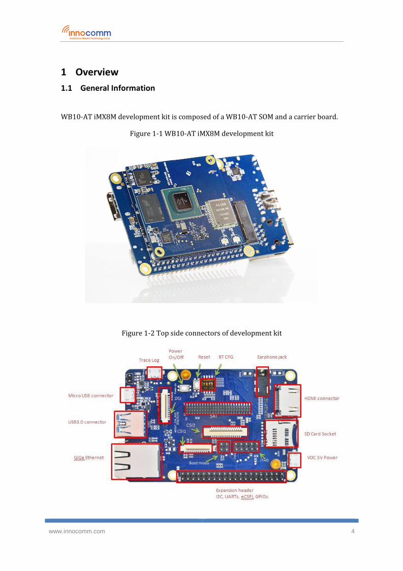
WB10-AT iMX8M development kit is composed of a WB10-AT SOM and a carrier board.
Figure 1-1 WB10-AT iMX8M development kit
Figure 1-2 Top side connectors of development kit

www.innocomm.com 5
Figure 1-3 Bottom side connectors of development kit
WB10-AT i.MX8M SOM is a high-performance System on Module (SOM) which is
designed based on NXP® i.MX 8M Quad processor. The i.MX 8M Quad integrates four
ARM® Cotex-A53 up to 1.5GHz and one Cotex-M4 cores to provide industry-leading
audio voice and video processing for applications that scale from consumer home audio
to home & building automation, voice assistance & machine vision, healthcare industry,
etc. It supports video quality with full 4K Ultra HD resolution and supports the highest
levels of pro audio fidelity with more than 20 audio channels each @384KHz as well.
WB10-AT SOM module offers a wide range of interfaces - GPIOs, PWM, I2C, SPI, CSI, DSI,
HDMI, UART, USB 3.0 and synchronous audio interface (SAI) that supports full duplex
serial interfaces with frame synchronization, such as I2S, AC97, TDM, and codec/DSP
interfaces. Moreover, this module features an Ethernet PHY on the module to support
Gigabits Ethernet Transceiver with HP Auto-MDIX.
It targets a wide range of embedded products such as medical devices, industrial
automation, Human Machine Interfaces (HMI), data acquisition, and much more.

www.innocomm.com 6
1.2 Architecture and Block Diagram
Figure 1-4 WB10-AT System Block Diagram
1.3 Feature Summary
NXP i.MX 8M
1GB LPDDR4 RAM
4GB eMMC
HDMI2.0a output
www.innocomm.com 7
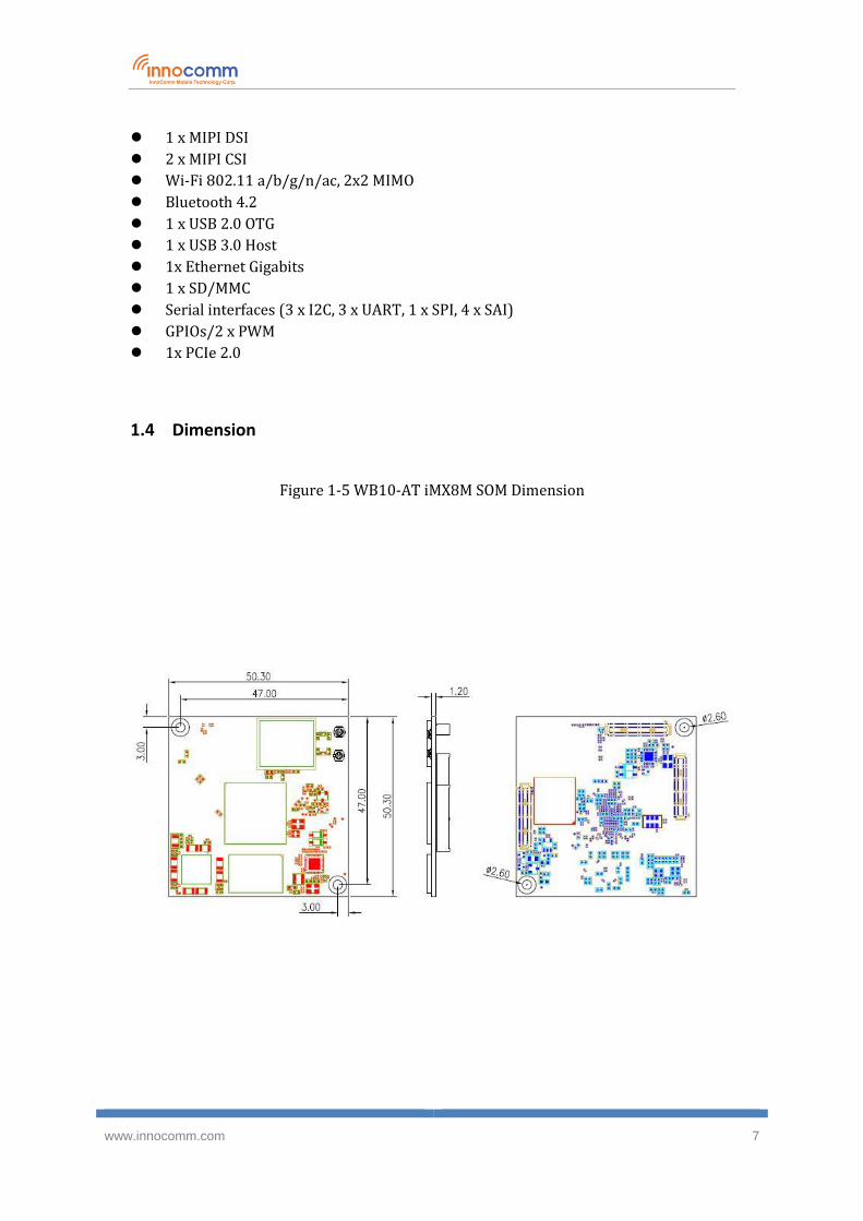
1 x MIPI DSI
2 x MIPI CSI
Wi-Fi 802.11 a/b/g/n/ac, 2x2 MIMO
Bluetooth 4.2
1 x USB 2.0 OTG
1 x USB 3.0 Host
1x Ethernet Gigabits
1 x SD/MMC
Serial interfaces (3 x I2C, 3 x UART, 1 x SPI, 4 x SAI)
GPIOs/2 x PWM
1x PCIe 2.0
1.4 Dimension
Figure 1-5 WB10-AT iMX8M SOM Dimension
www.innocomm.com 8
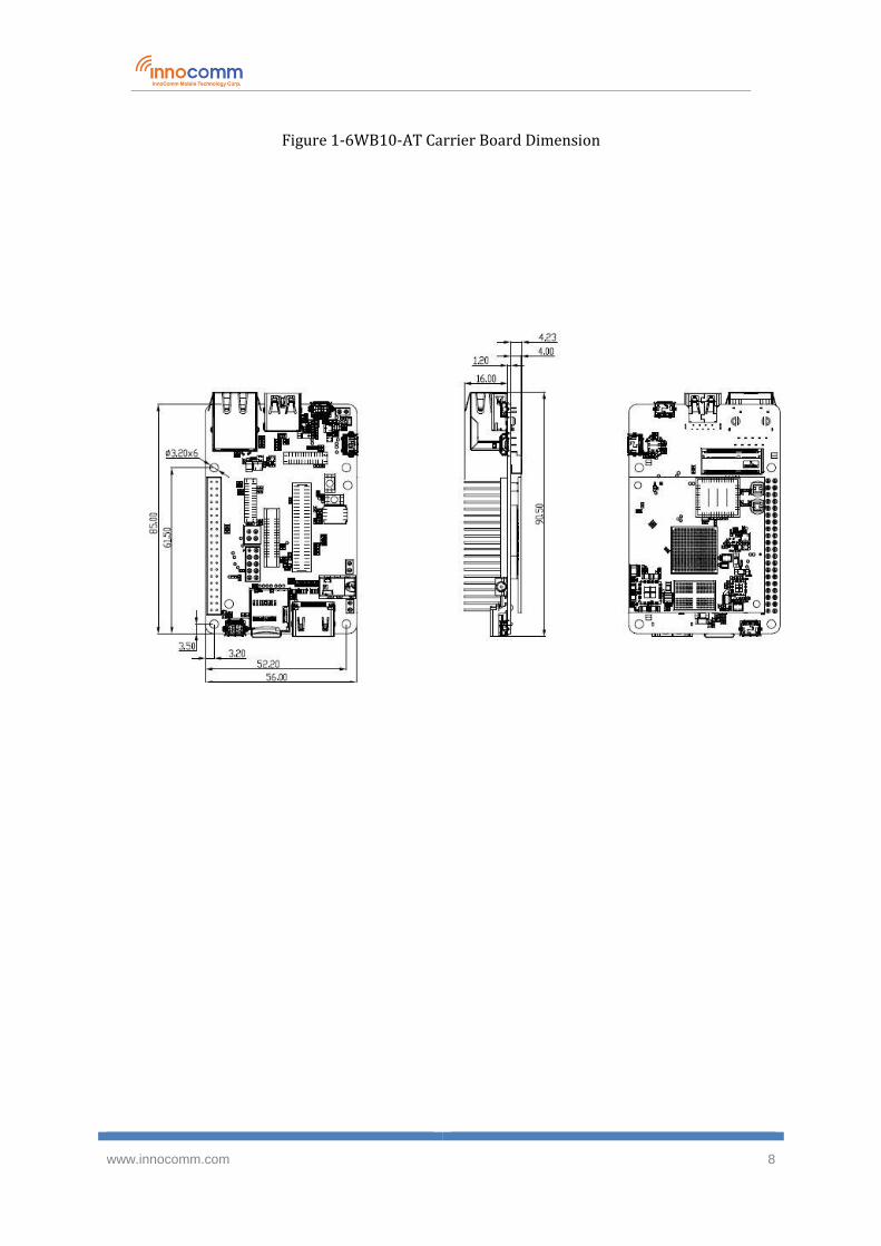
Figure 1-6WB10-AT Carrier Board Dimension
www.innocomm.com 9
2 Main Hardware Components
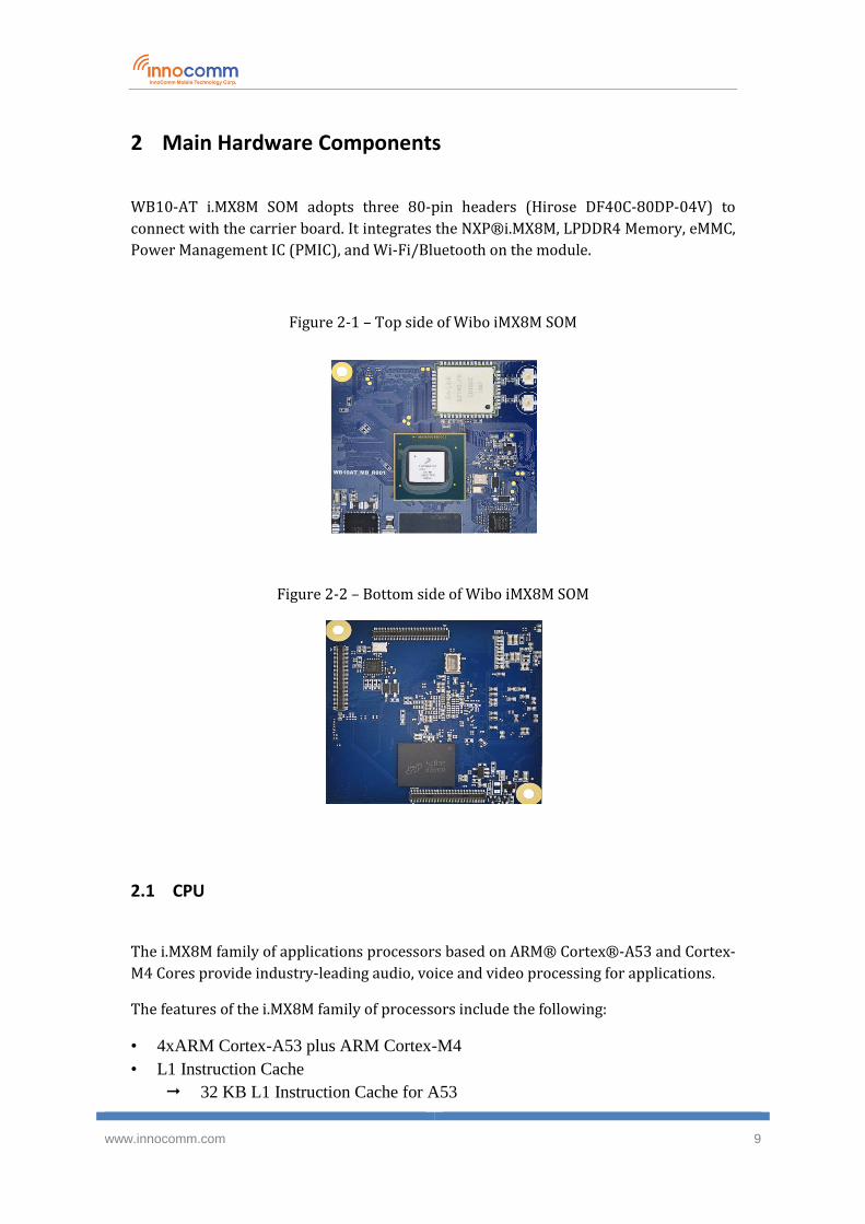
WB10-AT i.MX8M SOM adopts three 80-pin headers (Hirose DF40C-80DP-04V) to
connect with the carrier board. It integrates the NXP®i.MX8M, LPDDR4 Memory, eMMC,
Power Management IC (PMIC), and Wi-Fi/Bluetooth on the module.
Figure 2-1 – Top side of Wibo iMX8M SOM
Figure 2-2 – Bottom side of Wibo iMX8M SOM
2.1 CPU
The i.MX8M family of applications processors based on ARM® Cortex®-A53 and Cortex-
M4 Cores provide industry-leading audio, voice and video processing for applications.
The features of the i.MX8M family of processors include the following:
• 4xARM Cortex-A53 plus ARM Cortex-M4
• L1 Instruction Cache
32 KB L1 Instruction Cache for A53

www.innocomm.com 10
16 KB L1 instruction Cache for M4
• L1 Data Cache (each core)
32 KB L1 Data Cache (A7)
16 KB L1 Data Cache (M4)
• The ARM Cortex-A53 Core complex shares
General interrupt controller (GIC)
Global timer
Snoop control unit (SCU)
Unified instruction and data (1MB)
2.2 Memory
WB10-AT i.MX8M SOM is available with up to 3GB of LPDDR4 memory. The default
configuration is 1GB LPDDR4.
2.3 Power Management IC
WB10-AT i.MX8M SOM features Rohm BD7183MWV power management IC.
BD7183MWV is a programmable power management IC that integrates 8 buck
regulators and 7 LDOs to provide all power rails required by SoC and peripherals.
For system management, it provides the following features,
Support software shutdown or hardware power off
External wakeup source
Output monitor
PWROK signal for reset or power off
OVP, UVLO, TSD
2.4 eMMC Storage
The onboard eMMC device is connected on the SD1 pins of the i.MX8M processor in an 8-
bit width configuration.

www.innocomm.com 11
2.5 Wi-Fi/Bluetooth Module
The WB10-AT iMX8M SOM adopts Fn-Link 8274B combo module that integrates
wireless local area network 802.11a/b/g/n/ac2x2 MIMO and Bluetooth 4.2

www.innocomm.com 12
3 Interfaces and Connectors WB10-AT SOM is equipped with three Hirose DF40C-80DP-04Vconnectors- CON2401,
CON2501 and CON2601 to connected with Carrier board.
Below are the detail pin assignments and functionality of both SOM and carrier board.
3.1 SOMCON2601 Connector
Table 3-1 SOM CNO2601 Connector
CON2601
Pin# Signal Name
i.MX8
Pin # i.MX8 Ball Name
CON2601
Pin# Signal Name
i.MX8
Pin # i.MX8 Ball Name
1 PWRON_B . 2 VDD_SD2 .
3 BTB_GPIO5_IO7 A4 ECSPI1_MOSI 4 VDD_ETH_3V3 .
5 BTB_GPIO5_IO6 D5 ECSPI1_SCLK 6 GND .
7 GND . 8 GPIO3_IO6 G20
9 PCIE2_RXM D24 10 GPIO3_IO12 L19
11 PCIE2_RXP D25 12 GPIO3_IO15 K19
13 GND . 14 GPIO3_IO7 J20
15 PCIE2_TXM E24 16 GPIO3_IO16 K20
17 PCIE2_TXP E25 18 GPIO3_IO10 L20
19 GND . 20 GPIO3_IO8 H22
21 PCIE2_REF_CLKM F24 22 GPIO3_IO11 J22
23 PCIE2_REF_CLKP F25 24 GPIO3_IO9 J21
25 GND . 26 GPIO3_IO18 K21
27 GPIO3_IO17 K22 28 GND .
29 SD2_CLK L22 30 SD2_WP M21
31 GPIO3_IO14 M20 32 SD2_CMD M22
33 GPIO3_IO13 M19 34 SD2_DATA0 N22
35 SD2_DATA3 P21 36 SD2_DATA1 N21
37 SD2_nRST R22 38 SD2_DATA2 P22
39 SD2_nSDCD L21 40 GND .
41 JTAG_TCK T5 42 JTAG_TMS V5
43 JTAG_nTRST U6 44 JTAG_TDO U5
45 GND . 46 BOOT_MODE1 V6
47 ETHER_TRXN3 . 48 BOOT_MODE0 W6
49 ETHER_TRXP3 . 50 JTAG_TDI W5
51 GND . 52 ONOFF W21 ONOFF
53 ETHER_TRXN2 . 54 GND .
55 ETHER_TRXP2 . 56 LED_1000 .
57 GND . 58 LED_ACT .
59 ETHER_TRXN1 . 60 SYS_nRST .
61 ETHER_TRXP1 . 62 VDD_1V8 .
63 GND . 64 VDD_1V8 .

www.innocomm.com 13
65 ETHER_TRXN0 . 66 VDD_SNVS_3V3 .
67 ETHER_TRXP0 . 68 PORn W20 POR_B
69 GND . 70 GND .
71 VDC_5V . 72 VDC_5V .
73 VDC_5V . 74 VDC_5V .
75 VDC_5V . 76 VDC_5V .
77 VDC_5V . 78 VDC_5V .
79 VDC_5V . 80 VDC_5V .
www.innocomm.com 14
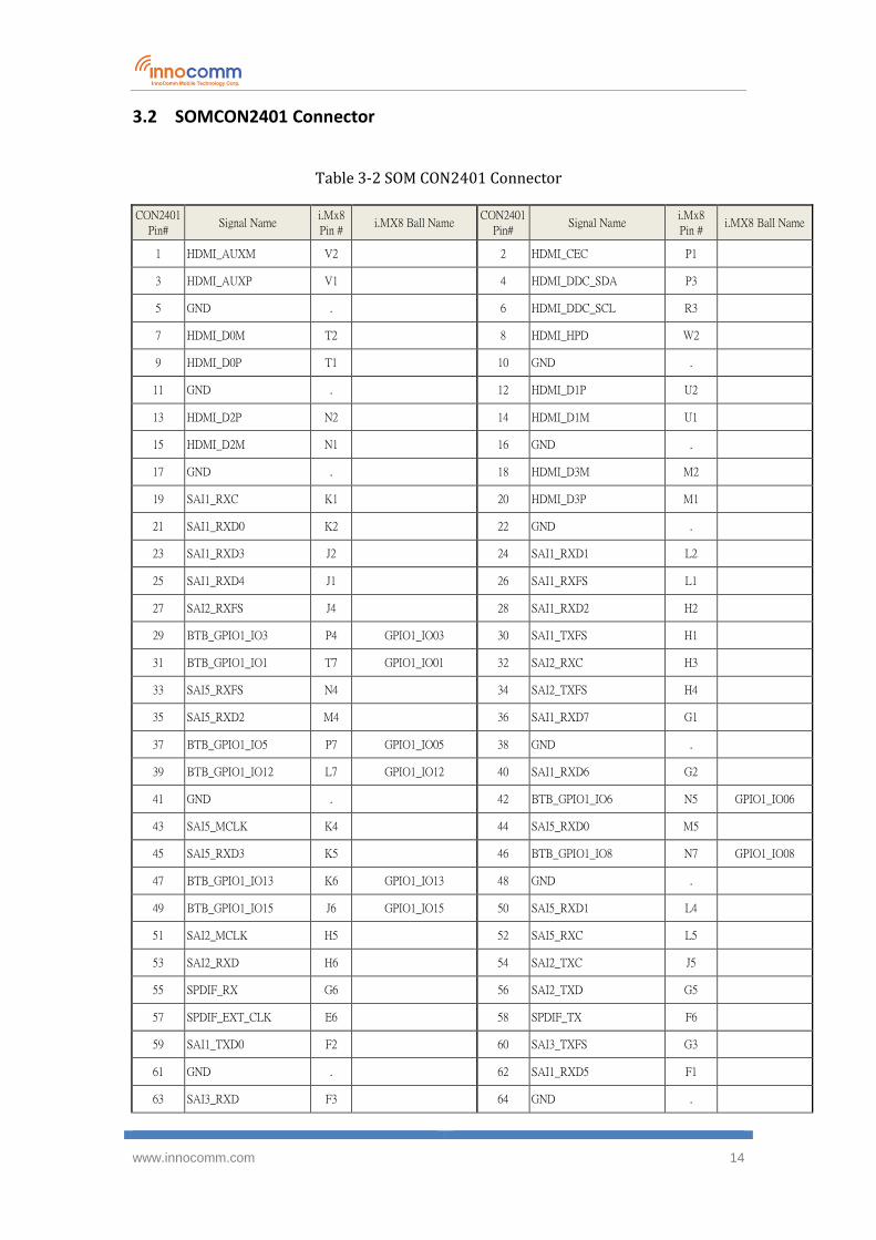
3.2 SOMCON2401 Connector
Table 3-2 SOM CON2401 Connector
CON2401
Pin# Signal Name
i.Mx8
Pin # i.MX8 Ball Name
CON2401
Pin# Signal Name
i.Mx8
Pin # i.MX8 Ball Name
1 HDMI_AUXM V2 2 HDMI_CEC P1
3 HDMI_AUXP V1 4 HDMI_DDC_SDA P3
5 GND . 6 HDMI_DDC_SCL R3
7 HDMI_D0M T2 8 HDMI_HPD W2
9 HDMI_D0P T1 10 GND .
11 GND . 12 HDMI_D1P U2
13 HDMI_D2P N2 14 HDMI_D1M U1
15 HDMI_D2M N1 16 GND .
17 GND . 18 HDMI_D3M M2
19 SAI1_RXC K1 20 HDMI_D3P M1
21 SAI1_RXD0 K2 22 GND .
23 SAI1_RXD3 J2 24 SAI1_RXD1 L2
25 SAI1_RXD4 J1 26 SAI1_RXFS L1
27 SAI2_RXFS J4 28 SAI1_RXD2 H2
29 BTB_GPIO1_IO3 P4 GPIO1_IO03 30 SAI1_TXFS H1
31 BTB_GPIO1_IO1 T7 GPIO1_IO01 32 SAI2_RXC H3
33 SAI5_RXFS N4 34 SAI2_TXFS H4
35 SAI5_RXD2 M4 36 SAI1_RXD7 G1
37 BTB_GPIO1_IO5 P7 GPIO1_IO05 38 GND .
39 BTB_GPIO1_IO12 L7 GPIO1_IO12 40 SAI1_RXD6 G2
41 GND . 42 BTB_GPIO1_IO6 N5 GPIO1_IO06
43 SAI5_MCLK K4 44 SAI5_RXD0 M5
45 SAI5_RXD3 K5 46 BTB_GPIO1_IO8 N7 GPIO1_IO08
47 BTB_GPIO1_IO13 K6 GPIO1_IO13 48 GND .
49 BTB_GPIO1_IO15 J6 GPIO1_IO15 50 SAI5_RXD1 L4
51 SAI2_MCLK H5 52 SAI5_RXC L5
53 SAI2_RXD H6 54 SAI2_TXC J5
55 SPDIF_RX G6 56 SAI2_TXD G5
57 SPDIF_EXT_CLK E6 58 SPDIF_TX F6
59 SAI1_TXD0 F2 60 SAI3_TXFS G3
61 GND . 62 SAI1_RXD5 F1
63 SAI3_RXD F3 64 GND .
www.innocomm.com 15
65 SAI1_TXC E1 66 SAI3_RXFS G4
67 SAI1_TXD1 E2 68 SAI1_TXD3 D1
69 SAI3_RXC F4 70 SAI1_TXD4 D2
71 SAI1_TXD7 C1 72 SAI3_TXD C3
73 SAI1_TXD5 C2 74 SAI3_MCLK D3
75 GND . 76 GND .
77 SAI1_TXD2 B2 78 SAI1_TXD6 B3
79 SAI1_MCLK A3 80 SAI3_TXC C4
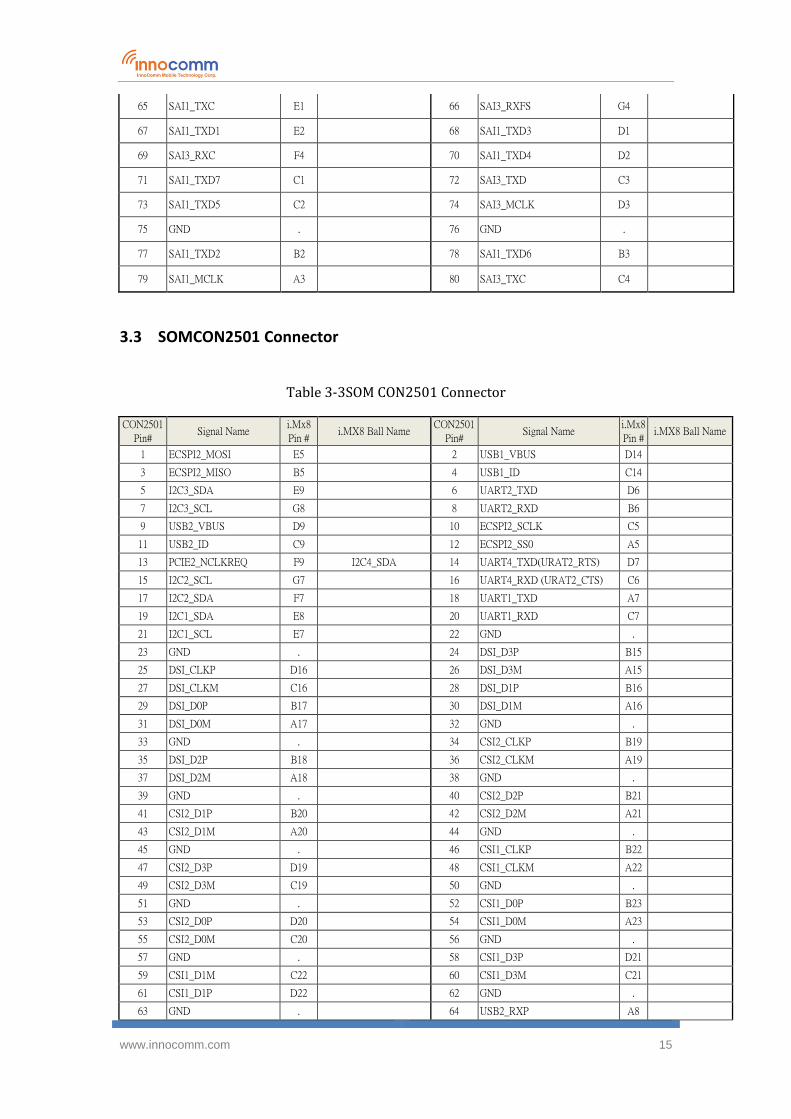
3.3 SOMCON2501 Connector
Table 3-3SOM CON2501 Connector
CON2501
Pin# Signal Name
i.Mx8
Pin # i.MX8 Ball Name
CON2501
Pin# Signal Name
i.Mx8
Pin # i.MX8 Ball Name
1 ECSPI2_MOSI E5 2 USB1_VBUS D14
3 ECSPI2_MISO B5 4 USB1_ID C14
5 I2C3_SDA E9 6 UART2_TXD D6
7 I2C3_SCL G8 8 UART2_RXD B6
9 USB2_VBUS D9 10 ECSPI2_SCLK C5
11 USB2_ID C9 12 ECSPI2_SS0 A5
13 PCIE2_NCLKREQ F9 I2C4_SDA 14 UART4_TXD(URAT2_RTS) D7
15 I2C2_SCL G7 16 UART4_RXD (URAT2_CTS) C6
17 I2C2_SDA F7 18 UART1_TXD A7
19 I2C1_SDA E8 20 UART1_RXD C7
21 I2C1_SCL E7 22 GND .
23 GND . 24 DSI_D3P B15
25 DSI_CLKP D16 26 DSI_D3M A15
27 DSI_CLKM C16 28 DSI_D1P B16
29 DSI_D0P B17 30 DSI_D1M A16
31 DSI_D0M A17 32 GND .
33 GND . 34 CSI2_CLKP B19
35 DSI_D2P B18 36 CSI2_CLKM A19
37 DSI_D2M A18 38 GND .
39 GND . 40 CSI2_D2P B21
41 CSI2_D1P B20 42 CSI2_D2M A21
43 CSI2_D1M A20 44 GND .
45 GND . 46 CSI1_CLKP B22
47 CSI2_D3P D19 48 CSI1_CLKM A22
49 CSI2_D3M C19 50 GND .
51 GND . 52 CSI1_D0P B23
53 CSI2_D0P D20 54 CSI1_D0M A23
55 CSI2_D0M C20 56 GND .
57 GND . 58 CSI1_D3P D21
59 CSI1_D1M C22 60 CSI1_D3M C21
61 CSI1_D1P D22 62 GND .
63 GND . 64 USB2_RXP A8

www.innocomm.com 16
65 CSI1_D2M B24 66 USB2_RXN B8
67 CSI1_D2P C23 68 USB2_TXP A9
69 GND . 70 USB2_TXN B9
71 USB2_DP A10 72 USB1_RXP A12
73 USB2_DN B10 74 USB1_RXN B12
75 USB1_DP A14 76 USB1_TXP A13
77 USB1_DN B14 78 USB1_TXN B13
79 VDDIO_3V3 . 80 VDDIO_3V3 .
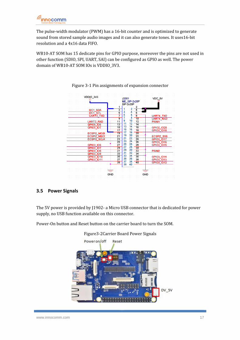
3.4 Carrier board Expansion Header
Expansion connector is a 40-pin header which contains I2Cs, UARTs, eCSPI, PWM, GPIOs
and power for user use.
UART interface support the following serial data transmit/receive protocols and
configurations:
• 7- or 8-bit data words, 1 or 2 stop bits, programmable parity (even, odd or none)
• Programmable baud rates up to 4 Mbps. This is a higher max baud rate relative to
the 1.875 MHz, which is stated by the TIA/EIA-232-F standard.
• 32-byte FIFO on Tx and 32 half-word FIFO on Rx supporting auto-baud
UART4_TXD, UART4_RXD can be configured as UART2_RTS and UART2_CTS respectively.
I2C interfaces which provide serial interface for external devices. Data rates of up to 400
kbps are supported
WB10-AT SOM supports one full-duplex Enhanced Configurable Serial Peripheral
Interface (ECSPI). The ECSPI contain a 64x32 receive buffer and a 64x32 transmit buffer.
The ECSPI power domain is VDDIO_3V3.
www.innocomm.com 17
The pulse-width modulator (PWM) has a 16-bit counter and is optimized to generate
sound from stored sample audio images and it can also generate tones. It uses16-bit
resolution and a 4x16 data FIFO.
WB10-AT SOM has 15 dedicate pins for GPIO purpose, moreover the pins are not used in
other function (SDIO, SPI, UART, SAI) can be configured as GPIO as well. The power
domain of WB10-AT SOM IOs is VDDIO_3V3.
Figure 3-1 Pin assignments of expansion connector
3.5 Power Signals
The 5V power is provided by J1902- a Micro USB connector that is dedicated for power
supply, no USB function available on this connector.
Power-On button and Reset button on the carrier board to turn the SOM.
Figure3-2Carrier Board Power Signals
www.innocomm.com 18
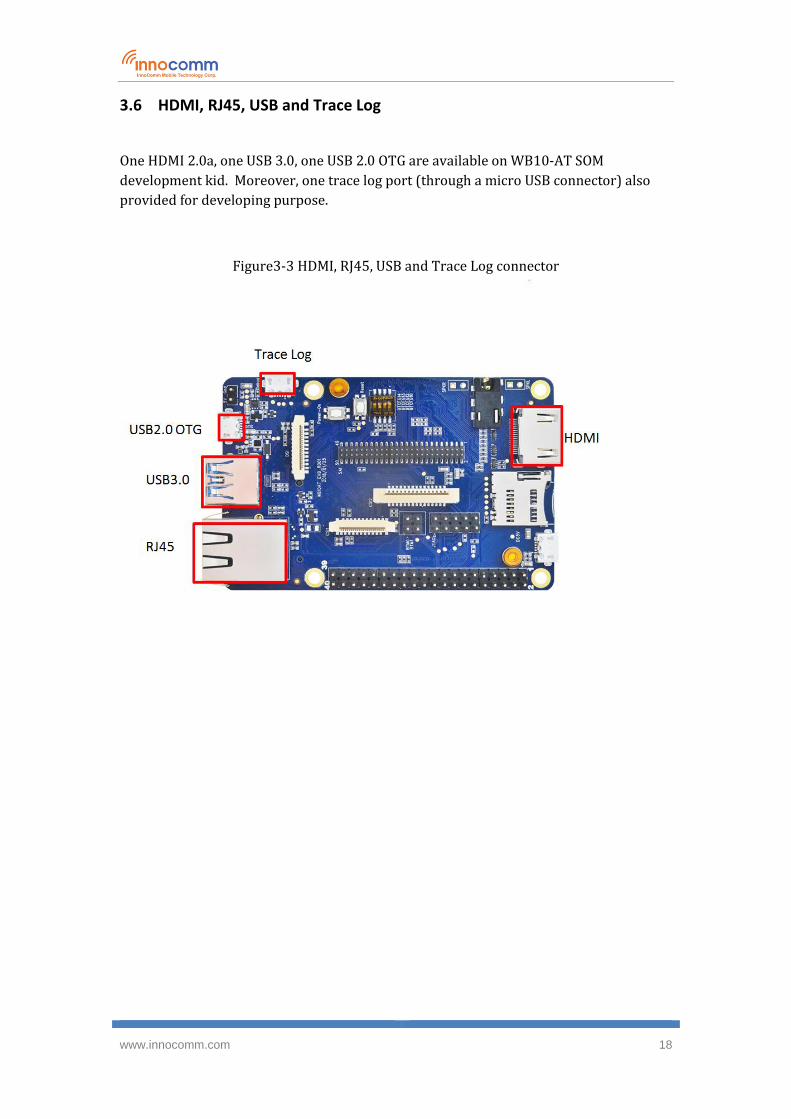
3.6 HDMI, RJ45, USB and Trace Log
One HDMI 2.0a, one USB 3.0, one USB 2.0 OTG are available on WB10-AT SOM
development kid. Moreover, one trace log port (through a micro USB connector) also
provided for developing purpose.
Figure3-3 HDMI, RJ45, USB and Trace Log connector
www.innocomm.com 19
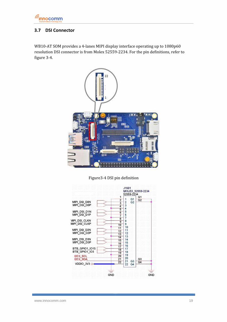
3.7 DSI Connector
WB10-AT SOM provides a 4-lanes MIPI display interface operating up to 1080p60
resolution DSI connector is from Molex 52559-2234. For the pin definitions, refer to
figure 3-4.
Figure3-4 DSI pin definition
www.innocomm.com 20
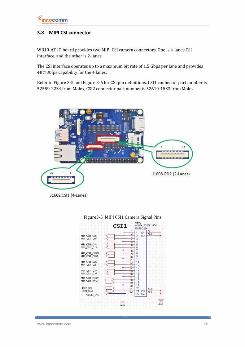
3.8 MIPI CSI connector
WB10-AT IO board provides two MIPI CSI camera connectors. One is 4-lanes CSI
interface, and the other is 2-lanes.
The CSI interface operates up to a maximum bit rate of 1.5 Gbps per lane and provides
4K@30fps capability for the 4 lanes.
Refer to Figure 3-5 and Figure 3-6 for CSI pin definitions. CSI1 connector part number is
52559-2234 from Molex, CSI2 connector part number is 52610-1533 from Molex.
Figure3-5 MIPI CSI1 Camera Signal Pins

www.innocomm.com 21
Figure3-5 MIPI CSI1 Camera Signal Pins
3.9 SD/MMC
Fully compatible with MMC command/response sets and Physical Layer as defined in
the Multimedia Card System Specification, v5.0/v4.4/v4.41/v4.4/v4.3/v4.2.
• Fully compatible with SD command/response sets and Physical Layer as defined in
the SD Memory Card Specifications v 3.0 including high-capacity SDXC cards up to 2
TB.
• Fully compatible with SDIO command/response sets and interrupt/Read-Wait mode
as defined in the SDIO Card Specification, Part E1, v. 3.0.
3.10 SAIs
The SAI interface provides a synchronous audio interface (SAI) that supports full duplex
serial interfaces with frame synchronization, such as I2S, AC97, TDM, and codec/DSP
interfaces.

www.innocomm.com 22
SAI2 is connected to the stereo CODEC, WM8960 in this design. WM8960 provides
stereo speaker output, stereo headset output and one MIC input.
Two 2-PIN headers next to earphone jack are the output of Left/Right speaker.
Headset L/R out and MIC in are connected to earphone jack. The pin definitions of SAI
and earphone jack are in Figure3-6 and Figure3-7.
Figure3-6 SAI Connector

www.innocomm.com 23
Figure 3-7 Earphone Pin definition
3.11 M.2 Connector
WB10-AT supports PCIe interface that is connected to M.2 connector from Amphenol
MDT420E01001 on bottom side of carrier board.
Pin definitions are shown in Figure3-8.

www.innocomm.com 24
Figure3-8 M.2 Connector
4 Reference Documents
1. i.MX 8M Family of Applications Processors Datasheet
2. i.MX 8M Family of Applications Processor Reference Manual
3. BD71837MWV Data sheet
4. Fn-Link 8274B Combo Wi-Fi Module Datasheet
5. LAN AR8035 Datasheet
6. WM8960 datasheet - Stereo CODEC with 1W Stereo Class D Speaker Drivers and
Headphone Drivers for Portable Audio Applications


