Organic ElectronicsStephen R. Forrest
Week 1-13
Thin Film Deposition, Processing and Patterning
Deposition from vapor (continued) & solutionPost-growth processing (annealing)
Device patterning
Chapter 5.4.2.4 - 5.6 (except 5.6.4)

Organic ElectronicsStephen R. Forrest
Crystal Platelets Grow on Cold Chamber Walls Via OVPD
• Same phenomenon as found in thermal gradient sublimation• Sometimes called ”plate sublimation”
rubrene pyrene
Karl, Organic Crystals, Springer (1980)de Boer et al. Phys. Stat. Sol. (a) 201 1302 (2004)
Organic ElectronicsStephen R. Forrest
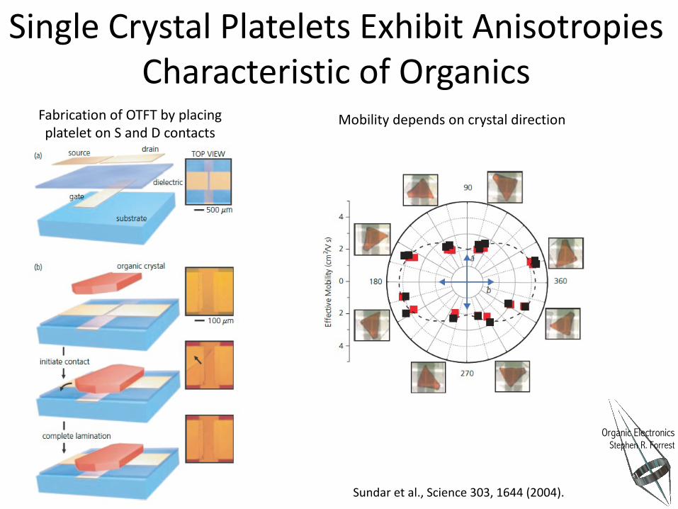
Single Crystal Platelets Exhibit Anisotropies Characteristic of Organics
Sundar et al., Science 303, 1644 (2004).
Fabrication of OTFT by placing platelet on S and D contacts
Mobility depends on crystal direction

Organic ElectronicsStephen R. Forrest
Solution Deposition: Common Methods
Spin-on
Drop fluid onto spinning substrate:Excess fluid thrown off
Evaporation rate = spin-off rate
Evaporation rate > spin-off rate: Film deposition complete
Doctor blade (Spread-on) Spray-on
Organic ElectronicsStephen R. Forrest
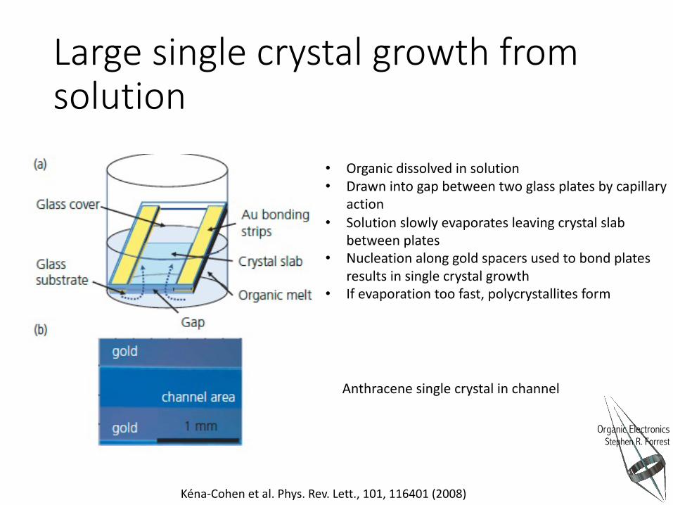
Large single crystal growth from solution
• Organic dissolved in solution • Drawn into gap between two glass plates by capillary
action• Solution slowly evaporates leaving crystal slab
between plates• Nucleation along gold spacers used to bond plates
results in single crystal growth• If evaporation too fast, polycrystallites form
Anthracene single crystal in channel
Kéna-Cohen et al. Phys. Rev. Lett., 101, 116401 (2008)

Organic ElectronicsStephen R. Forrest
Crystalline Growth from Solution Four methods that result in supersaturation of the solute in the
solvent, forcing crystallization
solvent evaporation temperature reduction
vapor diffusion• Source highly soluble in low volatility solvent 2• Less soluble in high volatility solvent 1• Solvent 1 concentration increases in inner
ampoule, resulting in supersaturation
liquid interdiffusion• Source highly soluble in solvent 2• Less soluble in solvent 1• Solvent 1 & 2 interdiffuse until supersaturation

Organic ElectronicsStephen R. Forrest
Langmuir-Blodgett Monolayer Film Deposition• Float molecules functionalized with hydrophilic and phobic groups on opposite ends on H2O• Draw hydrophilic or phobic sample surface through the film to pick up molecules• Squeeze film by bringing barriers in from edges of trough to “heal” the film hole• Repeat for as many cycles as MLs needed
Hydrophilic surface deposition Hydrophilic surface: layer 2 Hydrophobic surface deposition
Different configurations of 3 MLs on substrate surface
Organic ElectronicsStephen R. Forrest
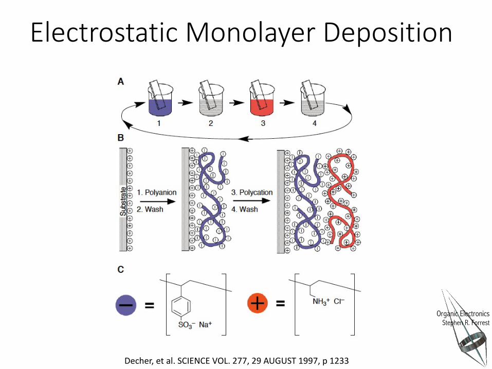
Electrostatic Monolayer Deposition
Decher, et al. SCIENCE VOL. 277, 29 AUGUST 1997, p 1233
Organic ElectronicsStephen R. Forrest
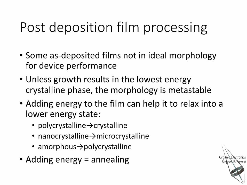
Post deposition film processing
• Some as-deposited films not in ideal morphology for device performance• Unless growth results in the lowest energy
crystalline phase, the morphology is metastable• Adding energy to the film can help it to relax into a
lower energy state:• polycrystalline→crystalline• nanocrystalline→microcrystalline• amorphous→polycrystalline
• Adding energy = annealing
Organic ElectronicsStephen R. Forrest
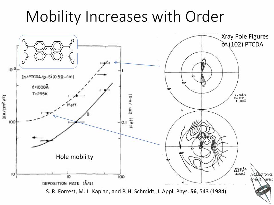
Mobility Increases with Order
S. R. Forrest, M. L. Kaplan, and P. H. Schmidt, J. Appl. Phys. 56, 543 (1984).
Hole mobiilty
O
O
O
O
O
O
Xray Pole Figuresof (102) PTCDA

Organic ElectronicsStephen R. Forrest
Film Annealing Processes
Source solution
Film coating
Non-equilibrium morphology
Thermal annealing
Thermodynamically driven reorganization
toward equilibriumSolvent vapor annealing
FIGURE ID: Fig05-052.epsIMAGE WIDTH X HEIGHT: 107.71 X 43.37MM
RESOLUTION/COLOR: N/A/N/AFILE SIZE: 0.45MB
Forrest
Near-equilibrium film morphology
Source solution
Film coating
Non-equilibrium morphology
Thermal annealing
Thermodynamically driven reorganization
toward equilibriumSolvent vapor annealing
FIGURE ID: Fig05-052.epsIMAGE WIDTH X HEIGHT: 107.71 X 43.37MM
RESOLUTION/COLOR: N/A/N/AFILE SIZE: 0.45MB
ForrestSource solution
Film coating
Non-equilibrium morphology
Thermal annealing
Thermodynamically driven reorganization
toward equilibriumSolvent vapor annealing
FIGURE ID: Fig05-052.epsIMAGE WIDTH X HEIGHT: 107.71 X 43.37MM
RESOLUTION/COLOR: N/A/N/AFILE SIZE: 0.45MB
Forrest
Film coating
Source solution
Film coating
Non-equilibrium morphology
Thermal annealing
Thermodynamically driven reorganization
toward equilibriumSolvent vapor annealing
FIGURE ID: Fig05-052.epsIMAGE WIDTH X HEIGHT: 107.71 X 43.37MM
RESOLUTION/COLOR: N/A/N/AFILE SIZE: 0.45MB
Forrest
Thermal annealing
Increase molecular mobility within the film byAdding heatIntroducing small solvent molecules

Organic ElectronicsStephen R. Forrest
Thermal annealing can be constrained with a capping layer
as-deposited 550K500 K450K
15 min anneal with Ag cap to hold top surface flat
CuPc:PTCBI 4:1
atom-atom potential structure calculation
Organic ElectronicsStephen R. Forrest
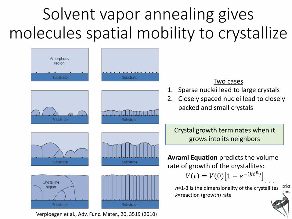
Solvent vapor annealing gives molecules spatial mobility to crystallize
Two cases1. Sparse nuclei lead to large crystals2. Closely spaced nuclei lead to closely
packed and small crystals
Crystal growth terminates when it grows into its neighbors
Avrami Equation predicts the volume rate of growth of the crystallites:
𝑉 𝑡 = 𝑉 0 1 − 𝑒! "#!
n=1-3 is the dimensionality of the crystallitesk=reaction (growth) rate
Verploegen et al., Adv. Func. Mater., 20, 3519 (2010)
Organic ElectronicsStephen R. Forrest
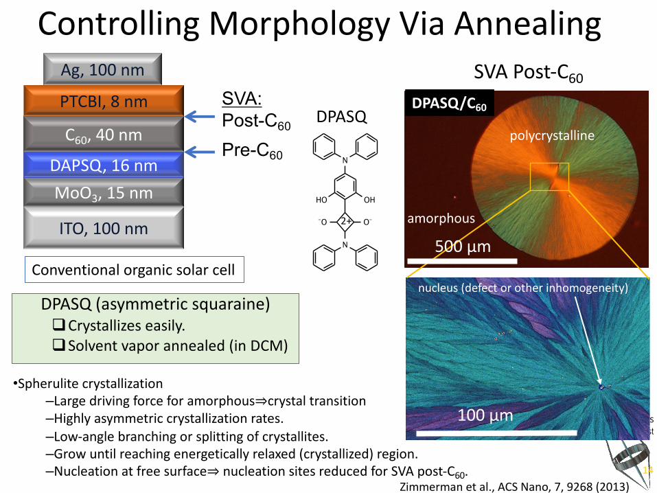
Controlling Morphology Via Annealing
DPASQ (asymmetric squaraine)qCrystallizes easily.qSolvent vapor annealed (in DCM)
14
2+
DPASQ
Conventional organic solar cell
DPASQ/C60
amorphous
polycrystalline
SVA Post-C60
100 μm
500 μm
MoO3, 15 nm
ITO, 100 nm
DAPSQ, 16 nm
C60, 40 nm
PTCBI, 8 nm
Ag, 100 nm
SVA:Post-C60Pre-C60
•Spherulite crystallization–Large driving force for amorphous⇒crystal transition–Highly asymmetric crystallization rates.–Low-angle branching or splitting of crystallites.–Grow until reaching energetically relaxed (crystallized) region.–Nucleation at free surface⇒ nucleation sites reduced for SVA post-C60.
nucleus (defect or other inhomogeneity)
Zimmerman et al., ACS Nano, 7, 9268 (2013)
Organic ElectronicsStephen R. Forrest
DPASQ:DPSQ+C60
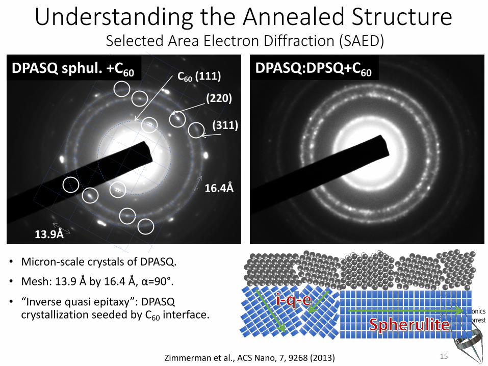
Understanding the Annealed StructureSelected Area Electron Diffraction (SAED)
15
13.9Å
16.4Å
C60 (111)
(220)
(311)
• Micron-scale crystals of DPASQ.
• Mesh: 13.9 Å by 16.4 Å, α=90°.
• “Inverse quasi epitaxy”: DPASQ crystallization seeded by C60 interface.
DPASQ sphul. +C60
Zimmerman et al., ACS Nano, 7, 9268 (2013)
Organic ElectronicsStephen R. Forrest
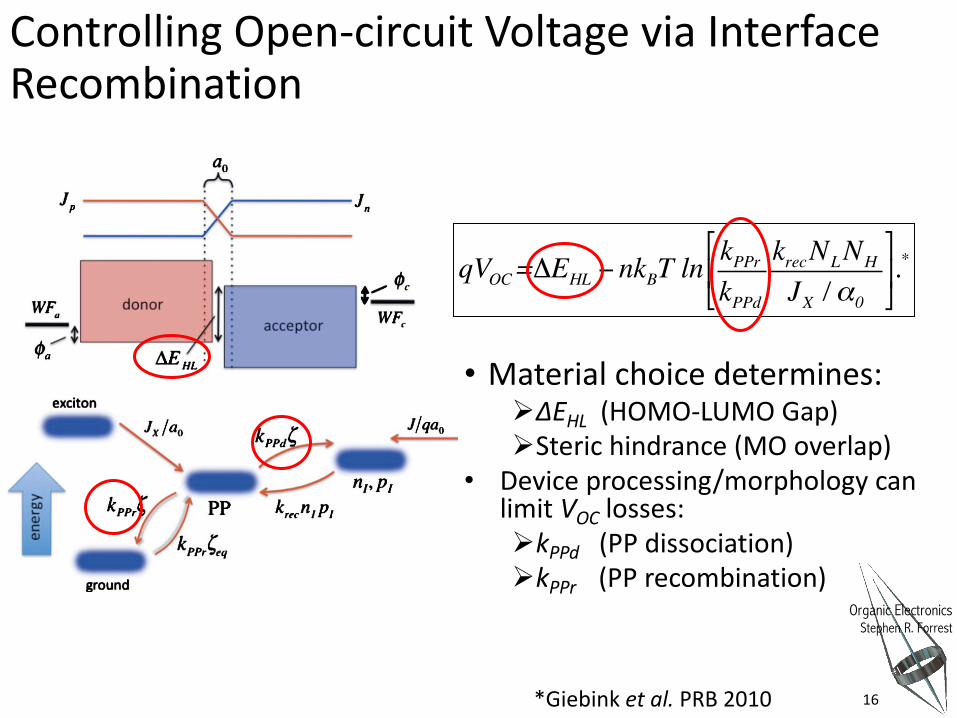
Controlling Open-circuit Voltage via Interface Recombination
qVOC=ΔEHL − nkBT ln kPPr
kPPd
krecNL NH
JX /α0
#
$%
&
'(.*
*Giebink et al. PRB 2010
• Material choice determines:ØΔEHL (HOMO-LUMO Gap)ØSteric hindrance (MO overlap)
• Device processing/morphology can limit VOC losses:ØkPPd (PP dissociation)ØkPPr (PP recombination)
16
Organic ElectronicsStephen R. Forrest
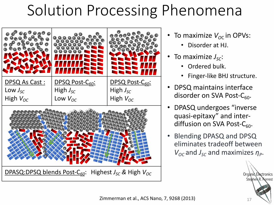
DPSQ As Cast :Low JSCHigh VOC
DPSQ Post-C60: High JSCLow VOC
DPSQ Post-C60:High JSCHigh VOC
DPASQ:DPSQ blends Post-C60: Highest JSC & High VOC
Solution Processing Phenomena
17
• To maximize VOC in OPVs:• Disorder at HJ.
• To maximize JSC:• Ordered bulk.• Finger-like BHJ structure.
• DPSQ maintains interface disorder on SVA Post-C60.
• DPASQ undergoes “inverse quasi-epitaxy” and inter-diffusion on SVA Post-C60.
• Blending DPASQ and DPSQ eliminates tradeoff between VOC and JSC and maximizes ηP.
Zimmerman et al., ACS Nano, 7, 9268 (2013)

Organic ElectronicsStephen R. Forrest
Device and Film PatterningPrimary purpose is to define the device area, suited to its function
Example: Pixel micro-patterning in OLED displays
• Requirements ØSimpleØNon-destructive of the materials forming the deviceØAdaptable to large substrate areasØAdaptable to flexible substratesØRapid (for large scale manufacturing)
• MethodsØShadow maskingØDirect printing (Ink jet and OVJP)ØPhotolithographyØStamping and nanopatterningØLITI

Organic ElectronicsStephen R. Forrest
30 cm
s
s
l
t
10-5 – 10-10 Torr 10-1 – 10 Torr
Vacuum Evaporation Vapor Phase Depositionvs.
2Bk T
Pl
s×
=× ×
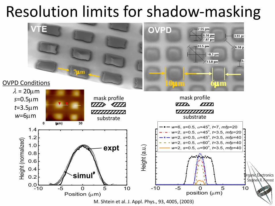
Shadow mask patterning in the kinetic and diffusive film growth regimes
M. Shtein et al. J. Appl. Phys., 93, 4005, (2003)
Mean free path
• Shadow mask patterning is the most common form of organic device electrode definition• Used for producing OLED displays for small mobile and large TV applications
Organic ElectronicsStephen R. Forrest
10µm 6µm7µm
VTE OVPD
-10 -5 0 5 100.00.20.40.60.81.01.21.4
Heigh
t (no
rmali
zed)
Position (µm)
OVPD Conditionsl = 20µms=0.5µmt=3.5µmw=6µm
0 30(µm)
-10 -5 0 5 10
Heigh
t (a.u
.)
position (µm)
w=6, s=0.5, a=45o, t=7, mfp=20 w=2, s=0.5, a=45o, t=3.5, mfp=20 w=2, s=0.5, a=45o, t=3.5, mfp=40 w=2, s=0.5, a=60o, t=3.5, mfp=40 w=2, s=0.5, a=90o, t=3.5, mfp=40
expt
simul’
Resolution limits for shadow-masking
M. Shtein et al. J. Appl. Phys., 93, 4005, (2003)
mask profile
substrate
mask profile
substrate
Organic ElectronicsStephen R. Forrest
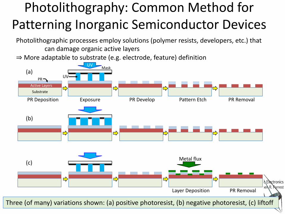
Substrate
(a)
(b)
(c)
Active LayersPR
UV Mask
PR Deposition Exposure PR Develop Pattern Etch PR Removal
Layer Deposition PR Removal
UV
Metal flux
Photolithography: Common Method for Patterning Inorganic Semiconductor Devices
Photolithographic processes employ solutions (polymer resists, developers, etc.) that can damage organic active layers
⇒ More adaptable to substrate (e.g. electrode, feature) definition
Three (of many) variations shown: (a) positive photoresist, (b) negative photoresist, (c) liftoff
Organic ElectronicsStephen R. Forrest
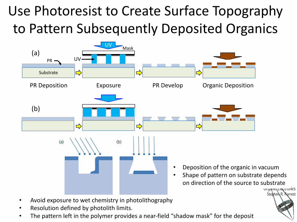
Substrate
(a)
(b)
PR
UV Mask
PR Deposition Exposure PR Develop Organic Deposition
UV
Use Photoresist to Create Surface Topography to Pattern Subsequently Deposited Organics
• Avoid exposure to wet chemistry in photolithography• Resolution defined by photolith limits.• The pattern left in the polymer provides a near-field “shadow mask” for the deposit
• Deposition of the organic in vacuum• Shape of pattern on substrate depends
on direction of the source to substrate

Organic ElectronicsStephen R. Forrest
Inkjet Printing
(a)
(b)
(c)
θσ sl σ sg
σ lg
• Organic semiconductors similar to inks used in printing• Organics must be soluble• Droplets injected into wells formed by polymer walls
• Film cross section depends on its rheological properties and relative energy with substrate surface
• “Coffee stain effect” encourages piling up of deposit near edges –can result in non-uniform device performance
Organic ElectronicsStephen R. Forrest
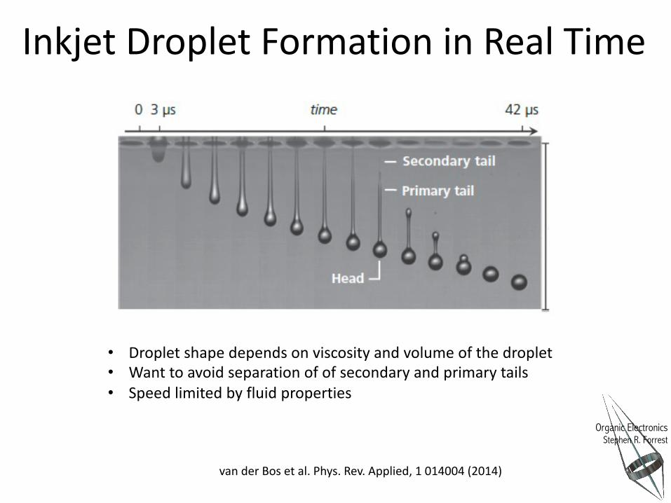
Inkjet Droplet Formation in Real Time
• Droplet shape depends on viscosity and volume of the droplet• Want to avoid separation of of secondary and primary tails• Speed limited by fluid properties
van der Bos et al. Phys. Rev. Applied, 1 014004 (2014)

Organic ElectronicsStephen R. Forrest
25
Printing an R-G-B WOLED Using Organic Vapor Jet Deposition
• Optimized R-G-B OLEDs can be combined to form a WOLED
• Each color separately optimized by choosing guest/host combinations
• Tunable color balance • Motion stage beneath nozzle• Nozzle creates high speed vapor jet
Arnold et al. Appl. Phys. Lett., 92, 053301 (2008)
Organic ElectronicsStephen R. Forrest
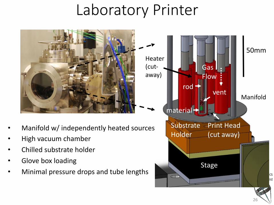
Laboratory Printer
50mm
Stage
SubstrateHolder
Heater(cut-away)
ventrod
material
Print Head(cut away)
Manifold
GasFlow
• Manifold w/ independently heated sources• High vacuum chamber• Chilled substrate holder• Glove box loading• Minimal pressure drops and tube lengths
26
Organic ElectronicsStephen R. Forrest
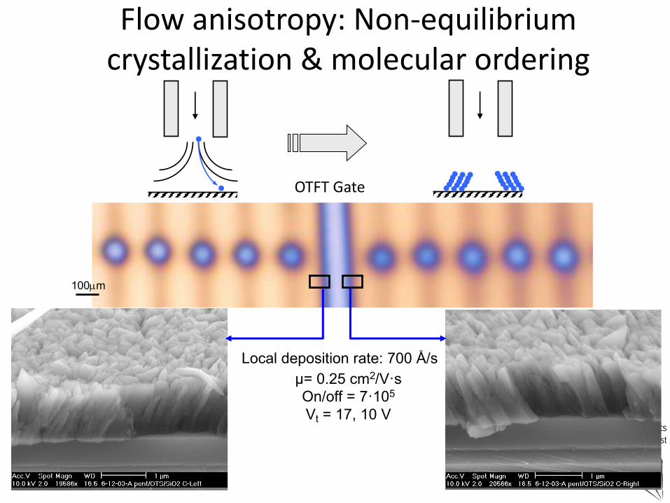
100µm
Flow anisotropy: Non-equilibrium crystallization & molecular ordering
Local deposition rate: 700 Å/sµ= 0.25 cm2/V·sOn/off = 7·105Vt = 17, 10 V
OTFT Gate

Organic ElectronicsStephen R. Forrest
Flow Dynamics That Govern OVJP Deposit Shape
• Nozzles “focus” molecular plus carrier gas flows toward the substrate• Heavier molecules (Alq3 in this example) take straigher trajectories and deposit nearly
directly under nozzle• Lighter carrier gas (N2) exhausts laterally• Flow rates are 100’s of m/s creating a high dynamic pressure beneath the nozzle
Shtein et al., J. Appl. Phys. 93,4005 (2003)

Organic ElectronicsStephen R. Forrest
Deposition ProfilesResolution Limits
g =10 μm
• deposit width increases with nozzle-substrate distance: g
• width increases with flow rate, Q, for small g• Shape of deposition profile accurately
reproduced by Monte Carlo simulations• 1.5 μm features possible
McGraw, et al. App. Phys. Lett. 8 013302 (2011) 29
sim
g=nozzle-substrate distance
20 µm nozzle width
Organic ElectronicsStephen R. Forrest
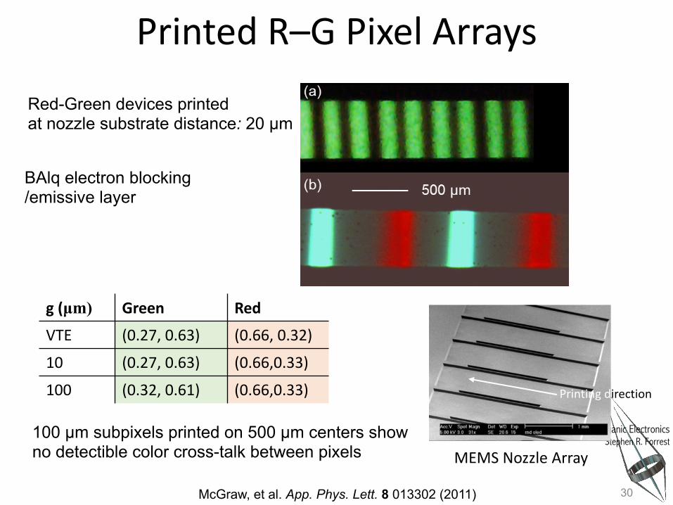
Printed R–G Pixel Arrays
BAlq electron blocking/emissive layer
100 μm subpixels printed on 500 μm centers showno detectible color cross-talk between pixels
g (μm) Green Red
VTE (0.27, 0.63) (0.66, 0.32)
10 (0.27, 0.63) (0.66,0.33)
100 (0.32, 0.61) (0.66,0.33)
30
MEMS Nozzle Array
Printing direction
McGraw, et al. App. Phys. Lett. 8 013302 (2011)
Red-Green devices printed at nozzle substrate distance: 20 μm

Organic ElectronicsStephen R. Forrest
Laser Induced Thermal Imaging (LITI)
Donor film
Substrate
Organic
Scanning laser beam
• High power laser beam absorbed in the donor film preloaded with the organic to be transferred
• Donor film placed in contact with substrate• Heat generated by laser volitalizes organic that transfers to the substrate in the
desired pattern
• Donor film must be replaced after each printing• Useful for sublimable materials (small molecules)• Radiation damage must be controlled by appropriate absorbing layer


