dpa-switch – 19.2 w dc-dc flyback converter with dpa425 · 36 vdc to 72 vdc input, +12v @ 0.8a,...
TRANSCRIPT
The products and applications illustrated herein (including circuits external to the products and transformer construction) may be covered by one or more U.S. and foreign patents or potentially by pending U.S. and foreign patent applications assigned to Power Integrations. A complete list of Power Integrations’ patents may be found at www.powerint.com
Power Integrations, Inc.
5245 Hellyer Avenue, San Jose, CA 95138 USA. Applications Hotline: Tel: +1 408 414 9660 Fax: +1 408 414 9760
www.powerint.com
Title DPA-Switch – 19.2 W DC-DC Flyback Converter with DPA425
Specification 36 VDC to 72 VDC Input, +12V @ 0.8A, -12V @ 0.8A Output
Application Telecom
Author RSP/RM
Document Number ASM-140197
Date 2/19/03
Revision 1 Features
• Low parts Count • Layout allows for tightly regulated +12V output or primary
side regulation with no opto-coupler for reduced parts count and lower cost

9/15/2014 ASM-140197
Page 2 of 21
Power Integrations, Inc. Tel: +1 408 414 9660 Fax: +1 408 414 9760 www.powerint.com
Table of Contents 1 Introduction ................................................................................................................. 3 2 Power Supply Specification ........................................................................................ 4 3 Schematic ................................................................................................................... 5
3.1 Circuit Operation ................................................................................................. 6 3.2 Input EMI filtering ................................................................................................ 6 3.3 Output Rectification ............................................................................................. 6 3.4 Output Feedback ................................................................................................. 6
4 Bill Of Materials .......................................................................................................... 7 4.1 Layout.................................................................................................................. 8
5 Design Spreadsheet ................................................................................................... 9 6 Transformer .............................................................................................................. 10 7 Performance Measurements .................................................................................... 12
7.1 Efficiency ........................................................................................................... 12 7.2 Regulation ......................................................................................................... 13
7.2.1 Load ........................................................................................................... 13 7.2.2 Line ............................................................................................................ 14
8 Waveforms ............................................................................................................... 15 8.1 Drain Voltage, Normal Operation ...................................................................... 15 8.2 Output Voltage Start-up Profile .......................................................................... 16 8.3 Output Ripple Measurements ............................................................................ 17
8.3.1 Ripple Measurement Technique ................................................................ 17 8.3.2 Measurement Results at 48 VDC ............................................................... 18
9 Revision History ........................................................................................................ 19

ASM-140197 9/15/2014
Page 3 of 21
Power Integrations, Inc.Tel: +1 408 414 9660 Fax: +1 408 414 9760
www.powerint.com
1 Introduction This document is an engineering report describing a dual output Flyback converter employing the DPA425R. The input voltage range is 36 to 72VDC providing a regulated +12V at 0.8A and a cross-regulated -12V @ 0.8A. The design also allow a primary-side regulation of the auxiliary winding that affords further parts count reduction and coarsely regulated +/-12V outputs. This document contains the power supply specification, schematic, and bill of materials, transformer documentation, printed circuit layout, and performance data.
Figure 1 - Populated Circuit Board.

9/15/2014 ASM-140197
Page 4 of 21
Power Integrations, Inc. Tel: +1 408 414 9660 Fax: +1 408 414 9760 www.powerint.com
2 Power Supply Specification
Description Symbol Min Typ Max Units Comment Input Voltage VIN 36 48 72 VDC No-load Input Power (60VDC) 0.75 W
Output Output Voltage 1 VOUT1 11.5 12.1 12.7 V ± 5% Output Ripple Voltage 1 VRIPPLE1 100 mV 20 MHz Bandwidth Output Current 1 IOUT1 0.8 A
Output Voltage 2 VOUT2 11.5 12.1 12.7 V ±5% Output Ripple Voltage 2 VRIPPLE2 100 mV 20 MHz Bandwidth Output Current 2 IOUT2 0.8 A
Total Output Power
Continuous Output Power POUT 19.6 W Peak Output Power POUT_PEAK W
Efficiency η 83 % Measured at Max. POUT, 25 oC
Ambient Temperature TAMB 0 40 oC Free convection, Sea level
ASM-140197 9/15/2014
Page 5 of 21
Power Integrations, Inc.Tel: +1 408 414 9660 Fax: +1 408 414 9760
www.powerint.com
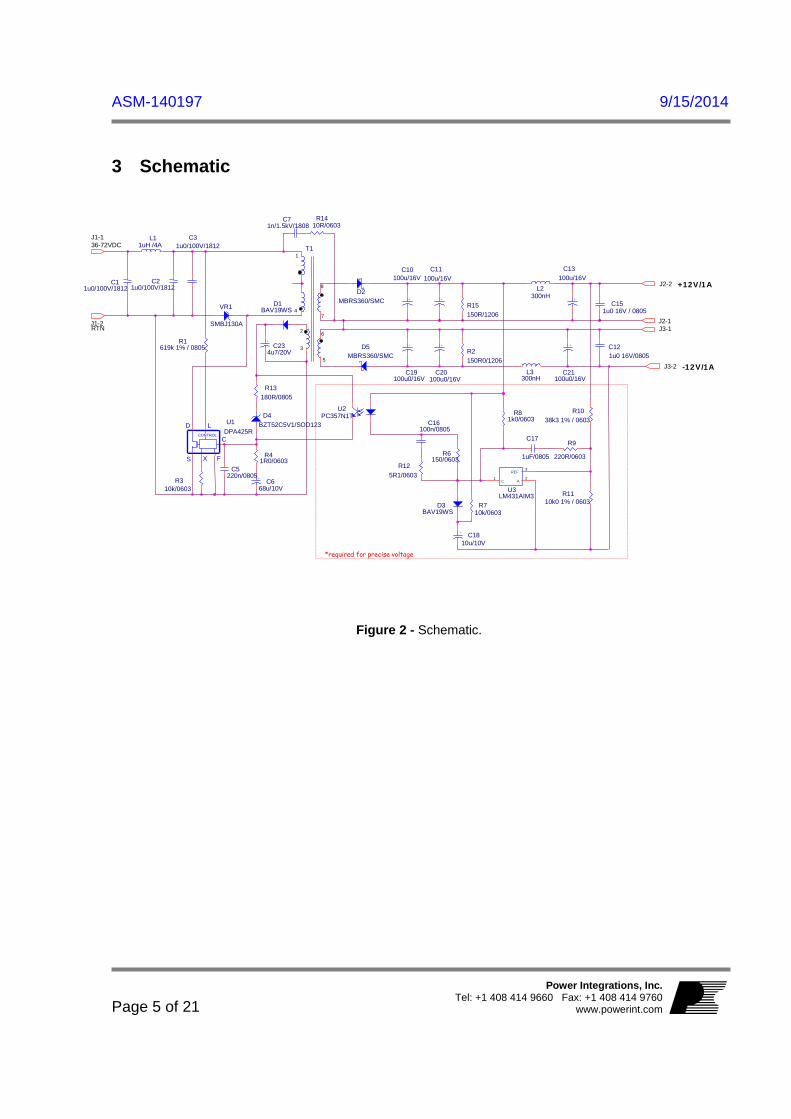
3 Schematic
Figure 2 - Schematic.
RTN
*required for precise voltage
VR1 SMBJ130A
+
C19100u0/16V
C17
1uF/0805
J1-2 J3-1
L3300nH
+ C1810u/10V
U2PC357N1T
-12V/1A
R1410R/0603
2
R3 10k/0603
F
D
S C
L CONTROL
X
U1DPA425R
L1 1uH /4A C3
1u0/100V/1812
8 J2-2
R6150/0603
U3LM431AIM3
1 2
3
C A
REF
D3BAV19WS
6 3 +
C23 4u7/20V
+
C11100u/16V
5
R9 220R/0603
D4 BZT52C5V1/SOD123
C1 1u0/100V/1812
+
C20100u0/16V
+ C6 68u/10V
C7 1n/1.5kV/1808
J3-2
R13 180R/0805
D1 BAV19WS
R81k0/0603
+
C10100u/16V
D2MBRS360/SMC
1
+12V/1A
C15 1u0 16V / 0805
R10 38k3 1% / 0603
R4 1R0/0603
36-72VDC
C2 1u0/100V/1812
R15150R/1206
C5220n/0805
R710k/0603
R1 619k 1% / 0805
4
L2300nH
R125R1/0603
J2-1
R11 10k0 1% / 0603
+
C13 100u/16V
J1-1
+
C21 100u0/16V
7
R2150R0/1206
C16100n/0805
D5MBRS360/SMC
C12 1u0 16V/0805
T1

9/15/2014 ASM-140197
Page 6 of 21
Power Integrations, Inc. Tel: +1 408 414 9660 Fax: +1 408 414 9760 www.powerint.com
3.1 Circuit Operation
3.2 Input EMI filtering Figure 1 shows a single-ended Flyback converter using the DPA425R. The circuit is designed for 36 V to 72 V input range and +/-12 V, 0.8A outputs. C1 and L1 provide input filtering. C2 and C3 bypass the DC rail. The DC rail is applied to the primary winding of T1. The other side of the transformer primary is driven by the integrated MOSFET in U1. VR1 clamps the U1 drain leakage spikes. R1 is used to set the low line turn-on threshold to approximately 33 V, and also sets the over-voltage shutdown level to approximately 88 V. C5 bypasses the U1 control pin, and provides the peak current necessary for driving the DPA-Switch internal MOSFET. C6 has three functions. It provides the energy required by U1 during startup, sets the auto-restart frequency during fault conditions, and also reduces the gain of U1 as a function of frequency. R4 adds a zero to stabilize the power supply control loop.
3.3 Output Rectification The output of T1 is rectified and filtered by D2 (D3) and C10-11 (C19-C20). L2 (L3) and C13 (C21) provides additional high frequency filtering. R2 (R15) damps primary to secondary circulating current, which would otherwise appear imposed on the output ripple voltage. An auxiliary Flyback winding on T1 powers U1 during normal operation. This winding delivers energy during the off time of U1, with an output voltage proportional to the supply output voltage. The turns-ratio of T1 sets the output voltage of the auxiliary winding to approximately 12 V. D1 and C23 rectify and filter the auxiliary winding output.
3.4 Output Feedback R10 and R11 divide down the supply output voltage and apply it to the reference pin of error amplifier U3. U3 drives opto-coupler U2 through resistor R6 to provide feedback information to the CONTROL pin of U1. The opto-coupler output also provides power to U1 during normal operating conditions. D3 and C18 apply drive to the opto-coupler during supply startup to eliminate output voltage overshoot. D3 isolates C18 from the supply feedback loop after startup. R7 discharges C18 when the supply is off. R8 provides bias current to U3. C6, C16, C17, R4, R6, R9, and R12 all play a role in compensating the power supply control loop. C6 rolls off the gain of U1 at a relatively low frequency. R4 provides a zero to cancel the phase shift of C6. R6 sets the gain of the direct signal path from the supply output through U2 and U3. C17 and R9 roll off the gain of U3. R12 and C16 provide phase boost near the resonant frequency of the transformer and output capacitors to improve phase margin and stability.
ASM-140197 9/15/2014
Page 7 of 21
Power Integrations, Inc.Tel: +1 408 414 9660 Fax: +1 408 414 9760
www.powerint.com
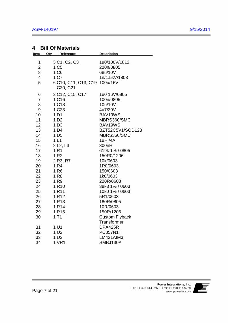
4 Bill Of Materials
Item Qty Reference Description
1 3 C1, C2, C3 1u0/100V/1812 2 1 C5 220n/0805 3 1 C6 68u/10V 4 1 C7 1n/1.5kV/1808 5 6 C10, C11, C13, C19
C20, C21 100u/16V
6 3 C12, C15, C17 1u0 16V/0805 7 1 C16 100n/0805 8 1 C18 10u/10V 9 1 C23 4u7/20V
10 1 D1 BAV19WS 11 1 D2 MBRS360/SMC 12 1 D3 BAV19WS 13 1 D4 BZT52C5V1/SOD123 14 1 D5 MBRS360/SMC 15 1 L1 1uH /4A 16 2 L2, L3 300nH 17 1 R1 619k 1% / 0805 18 1 R2 150R0/1206 19 2 R3, R7 10k/0603 20 1 R4 1R0/0603 21 1 R6 150/0603 22 1 R8 1k0/0603 23 1 R9 220R/0603 24 1 R10 38k3 1% / 0603 25 1 R11 10k0 1% / 0603 26 1 R12 5R1/0603 27 1 R13 180R/0805 28 1 R14 10R/0603 29 1 R15 150R/1206 30 1 T1 Custom Flyback
Transformer 31 1 U1 DPA425R 32 1 U2 PC357N1T 33 1 U3 LM431AIM3 34 1 VR1 SMBJ130A
9/15/2014 ASM-140197
Page 8 of 21
Power Integrations, Inc. Tel: +1 408 414 9660 Fax: +1 408 414 9760 www.powerint.com
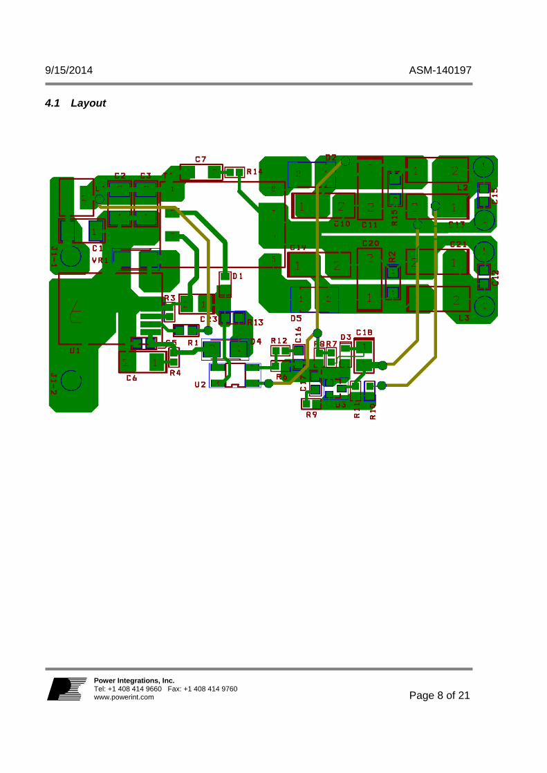
4.1 Layout
ASM-140197 9/15/2014
Page 9 of 21
Power Integrations, Inc.Tel: +1 408 414 9660 Fax: +1 408 414 9760
www.powerint.com
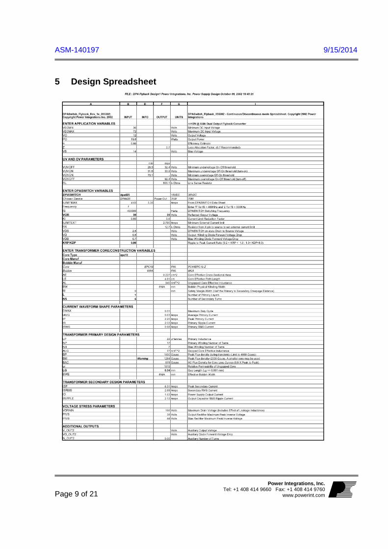
5 Design Spreadsheet
9/15/2014 ASM-140197
Page 10 of 21
Power Integrations, Inc. Tel: +1 408 414 9660 Fax: +1 408 414 9760 www.powerint.com
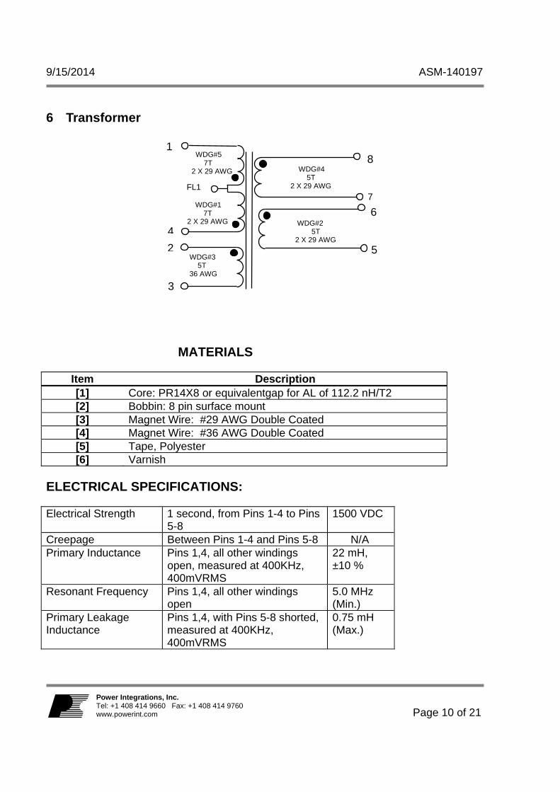
6 Transformer
MATERIALS
Item Description [1] Core: PR14X8 or equivalentgap for AL of 112.2 nH/T2 [2] Bobbin: 8 pin surface mount [3] Magnet Wire: #29 AWG Double Coated[4] Magnet Wire: #36 AWG Double Coated [5] Tape, Polyester [6] Varnish
ELECTRICAL SPECIFICATIONS:
Electrical Strength 1 second, from Pins 1-4 to Pins
5-8 1500 VDC
Creepage Between Pins 1-4 and Pins 5-8 N/APrimary Inductance Pins 1,4, all other windings
open, measured at 400KHz, 400mVRMS
22 mH, ±10 %
Resonant Frequency Pins 1,4, all other windings open
5.0 MHz (Min.)
Primary Leakage Inductance
Pins 1,4, with Pins 5-8 shorted, measured at 400KHz, 400mVRMS
0.75 mH (Max.)
8
7
WDG#4 5T 2 X 29 AWG
WDG#5 7T 2 X 29 AWG
1
4
FL1
WDG#1 7T 2 X 29 AWG
WDG#3 5T 36 AWG
2
3
WDG#2 5T 2 X 29 AWG
6
5

ASM-140197 9/15/2014
Page 11 of 21
Power Integrations, Inc.Tel: +1 408 414 9660 Fax: +1 408 414 9760
www.powerint.com
TRANSFORMER CONSTRUCTION
WINDING INSTRUCTIONS:
½ Primary Start at Pin 4. Wind 7 bifiliar turns of item [3]. Finish on Exit-finish lead at bobbin flange slot on primary side of bobbin, leaving 1” lead length.
Basic Insulation Use one layer of item [5] for basic insulation.
-12V Winding Start at Pin 6. Wind 5 bifiliar turns of item [3] Finish on Pin 5. Basic Insulation Use one layer of item [5] for basic insulation. Primary Bias Start at Pin 2. Wind 5 turns of item [4] Finish on Pin 3. Basic Insulation Use one layer of item [5] for basic insulation. +12V Winding Start at Pin 8. Wind 5 bifiliar turns of item [3] Finish on Pin 7. ½ Primary Start in bobbin flange slot on primary side of transformer
leave 1” lead length at start. Wind 7 bifiliar turns of item [3]. Finish on Pin 1.
Outer Wrap Wrap windings with 3 layers of tape [item [5]. Flying Lead Finish
Twist start of winding 4 together with finish of winding 2. Tin and trim to 1/8” length (FL1).
Final Assembly Assemble and secure core halves. Varnish and impregnate (item [6]).
Primary Bias
½ Primary
Tape5
4
3
FL ½ Primary
6 -12V Winding
1
8 +12V Winding7
2

9/15/2014 ASM-140197
Page 12 of 21
Power Integrations, Inc. Tel: +1 408 414 9660 Fax: +1 408 414 9760 www.powerint.com
7 Performance Measurements All measurements performed at room temperature.
7.1 Efficiency
0.00%
10.00%
20.00%
30.00%
40.00%
50.00%
60.00%
70.00%
80.00%
90.00%
100.00%
30 35 40 45 50 55 60 65
Input Voltage (VDC)
Effic
ienc
y (%
)
I (+12V) = I (-12V) =0.2A
"I (+12V) = I (-12V) =0.4A"
"I (+12V) = I (-12V) =0.6A"
"I (+12V) = I (-12V) =0.8A"
Efficiency vs. Input Voltage, Full Load, Room Temperature

ASM-140197 9/15/2014
Page 13 of 21
Power Integrations, Inc.Tel: +1 408 414 9660 Fax: +1 408 414 9760
www.powerint.com
7.2 Regulation
7.2.1 Load
11.5
11.7
11.9
12.1
12.3
12.5
12.7
0 0.1 0.2 0.3 0.4 0.5 0.6 0.7 0.8
Load Current (ADC)
|Out
put V
olta
ge| (
VDC
)
"Vout = +12V: Vin = 36V
Vout = -12V: Vin = 36V
"Vout = +12V: Vin = 48V
"Vout = -12V: Vin = 48V
"Vout = +12V: Vin = 60V
"Vout = -12V: Vin =60V
Load Regulation, enter conditions
9/15/2014 ASM-140197
Page 14 of 21
Power Integrations, Inc. Tel: +1 408 414 9660 Fax: +1 408 414 9760 www.powerint.com
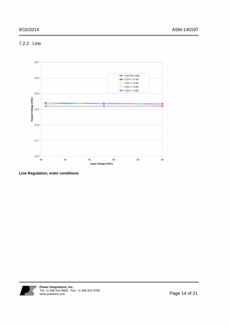
7.2.2 Line
11.5
11.7
11.9
12.1
12.3
12.5
12.7
35 40 45 50 55 60
Input Voltage (VDC)
Out
put V
olta
ge (V
DC
)
+12V No Load+12V I = 0.2A+12V I = 0.4A+12V I = 0.6A+12V I = 0.8A
Line Regulation, enter conditions
ASM-140197 9/15/2014
Page 15 of 21
Power Integrations, Inc.Tel: +1 408 414 9660 Fax: +1 408 414 9760
www.powerint.com
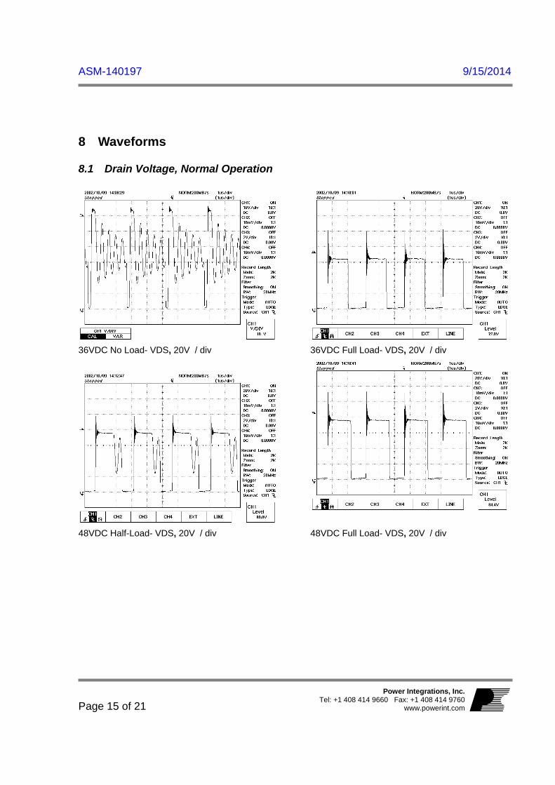
8 Waveforms
8.1 Drain Voltage, Normal Operation
36VDC No Load- VDS, 20V / div
48VDC Half-Load- VDS, 20V / div
36VDC Full Load- VDS, 20V / div
48VDC Full Load- VDS, 20V / div

9/15/2014 ASM-140197
Page 16 of 21
Power Integrations, Inc. Tel: +1 408 414 9660 Fax: +1 408 414 9760 www.powerint.com
63VDC No Load- VDS, 20V / div
63VDC Full Load- VDS, 20V / div
8.2 Output Voltage Start-up Profile
Start-up Profile, Vin = 48V, No Load (20msec/div) & (2V/div)
Start-up Profile, Vin = 48V, Full-Load (20msec/div) & (2V/div

ASM-140197 9/15/2014
Page 17 of 21
Power Integrations, Inc.Tel: +1 408 414 9660 Fax: +1 408 414 9760
www.powerint.com
8.3 Output Ripple Measurements
8.3.1 Ripple Measurement Technique For DC output ripple measurements, a modified oscilloscope test probe must be utilized in order to reduce spurious signals due to pickup. Details of the probe modification are provided in Figure 24 and Figure 25. The 5125BA probe adapter is affixed with two capacitors tied in parallel across the probe tip. The capacitors include one (1) 0.1 µF/50 V ceramic type and one (1) 1.0 µF/50 V aluminum electrolytic. The aluminum electrolytic type capacitor is polarized, so proper polarity across DC outputs must be maintained (see below).
Oscilloscope Probe Prepared for Ripple Measurement. (End Cap and Ground Lead Removed)
Oscilloscope Probe with Probe Master 5125BA BNC Adapter. (Modified with wires for probe ground for
ripple measurement, and two parallel decoupling capacitors added)
Probe Ground
Probe Tip

9/15/2014 ASM-140197
Page 18 of 21
Power Integrations, Inc. Tel: +1 408 414 9660 Fax: +1 408 414 9760 www.powerint.com
8.3.2 Measurement Results at 48 VDC
+12 V Ripple, No Load
2 us, 10 mV / div
+12 V Ripple, Full Load 2 us, 10 mV / div

9/15/2014 ASM-140197
Page 19 of 21
Power Integrations, Inc.Tel: +1 408 414 9660 Fax: +1 408 414
9760www.powerint.com
9 Revision History
Date Author Revision Description & changes 2/19/2003 RM 1 Initial Release

ASM-140197 9/15/2014
Page 20 of 21
Power Integrations, Inc. Tel: +1 408 414 9660 Fax: +1 408 414 9760 www.powerint.com
Notes

9/15/2014 ASM-140197
Page 21 of 21
Power Integrations, Inc.Tel: +1 408 414 9660 Fax: +1 408 414
9760www.powerint.com
For the latest updates, visit our website: www.powerint.com Power Integrations reserves the right to make changes to its products at any time to improve reliability or manufacturability. Power Integrations does not assume any liability arising from the use of any device or circuit described herein, nor does it convey any license under its patent rights or the rights of others. PI Logo, TOPSwitch and TinySwitch are registered trademarks of Power Integrations, Inc. ©Copyright 2001, Power Integrations, Inc. The products and applications illustrated herein (including circuits external to the products and transformer construction) may be covered by one or more U.S. and foreign patents or potentially by pending U.S. and foreign patent applications assigned to Power Integrations. A complete list of Power Integrations’ patents may be found at www.powerint.com. WORLD HEADQUARTERS AMERICAS Power Integrations, Inc. 5245 Hellyer Avenue San Jose, CA 95138 USA. Main: +1-408-414-9200 Customer Service: Phone: +1-408-414-9665 Fax: +1-408-414-9765 E-Mail: [email protected]
EUROPE & AFRICA Power Integrations (Europe) Ltd. Centennial Court Easthampstead Road Bracknell Berkshire RG12 1YQ, United Kingdom Phone: +44-1344-462-300 Fax: +44-1344-311-732 E-Mail: [email protected]
SINGAPORE Power Integrations, Singapore 51 Goldhill Plaza #16-05 Republic of Singapore 308900 Phone: +65-6358-2160 Fax: +65-6358-2015 E-Mail: [email protected]
TAIWAN Power Integrations International Holdings, Inc. 17F-3, No. 510, Chung Hsiao E. Rd., Sec. 5, Taipei, Taiwan 110, R.O.C. Phone: +886-2-2727-1221 Fax: +886-2-2727-1223 E-Mail: [email protected]
CHINA Power Integrations International Holdings, Inc. Rm# 1705, Bao Hua Bldg. 1016 Hua Qiang Bei Lu Shenzhen Guangdong, 518031, China Phone: +86-755-8367-5143 Fax: +86-755-8377-9610 E-Mail: [email protected]
KOREA Power Integrations International Holdings, Inc. 8th Floor, DongSung Building 17-8, Yoido-dong, Youngdeungpo-gu, Seoul, 150-874, Korea Phone: +82-2-782-2840 Fax: +82-2-782-4427 E-Mail: [email protected]
JAPANPower Integrations, K.K. Keihin-Tatemono 1st Bldg. 12-20 Shin-Yokohama 2-Chome, Kohoku-ku, Yokohama-shi, Kanagawa 222-0033, Japan Phone: +81-45-471-1021 Fax: +81-45-471-3717 E-Mail: [email protected]
INDIA (Technical Support)Innovatech #1, 8th Main Road Vasanthnagar Bangalore, India 560052 Phone: +91-80-226-6023 Fax: +91-80-228-9727 E-Mail: [email protected]
APPLICATIONS HOTLINEWorld Wide +1-408-414-9660
APPLICATIONS FAXWorld Wide +1-408-414-9760