dpg3 - farnell.com · and allows a user to download a data vector into the dpg3, ... on these pcs,...
TRANSCRIPT
One Technology Way · P.O. Box 9106 · Norwood, MA 02062-9106 · Tel: 781.329.4700 · Fax: 781.461.3113 · www.analog.com
Rev 26 Jun 2014 13:42 | Page 1
DPG3
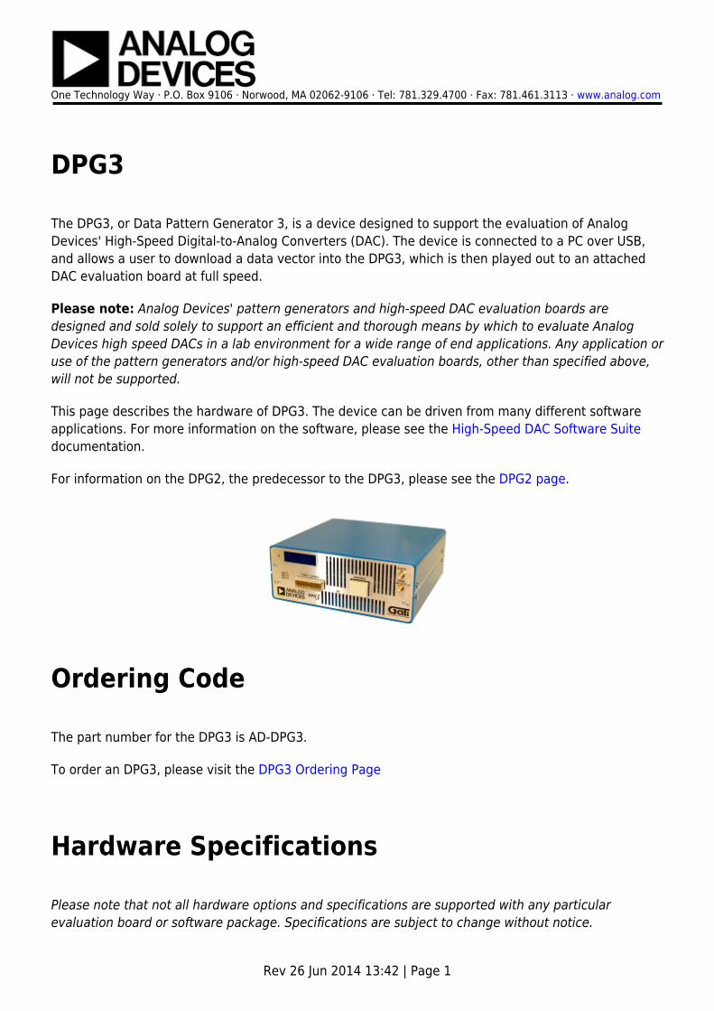
The DPG3, or Data Pattern Generator 3, is a device designed to support the evaluation of AnalogDevices' High-Speed Digital-to-Analog Converters (DAC). The device is connected to a PC over USB,and allows a user to download a data vector into the DPG3, which is then played out to an attachedDAC evaluation board at full speed.
Please note: Analog Devices' pattern generators and high-speed DAC evaluation boards aredesigned and sold solely to support an efficient and thorough means by which to evaluate AnalogDevices high speed DACs in a lab environment for a wide range of end applications. Any application oruse of the pattern generators and/or high-speed DAC evaluation boards, other than specified above,will not be supported.
This page describes the hardware of DPG3. The device can be driven from many different softwareapplications. For more information on the software, please see the High-Speed DAC Software Suitedocumentation.
For information on the DPG2, the predecessor to the DPG3, please see the DPG2 page.
Ordering Code
The part number for the DPG3 is AD-DPG3.
To order an DPG3, please visit the DPG3 Ordering Page
Hardware Specifications
Please note that not all hardware options and specifications are supported with any particularevaluation board or software package. Specifications are subject to change without notice.

Rev 26 Jun 2014 13:42 | Page 2
Converter Interfaces●
CMOS Interface❍
32-bits (shared with the P lines of the LVDS bus)■
Up to 250Mbps per bit(SDR)■
Same connector and pinout as DPG2■
LVDS Interface❍
32-bits (P lines shared with CMOS interface)■
Up to 1.6Gbps per bit (800MHz DDR)■
Same connector and pinout as DPG2■
High-Speed Serial Interface (For JESD204 Converters)❍
16 Tx lanes■
Up to 8.5Gbps per lane■
Memory●
Dual DDR3 SO-DIMM❍
Maximum pattern length of 134M samples (limited to 30M samples in most 3'rd party software)❍
PC Interface●
USB 2.0 “B” connector❍
Clocking●
On-connector clock input for all interfaces❍
Optional external clock input via front-panel SMA jack for CMOS and LVDS interfaces❍
Trigger●
SMA jack for trigger input or output❍
Specified for operation at 25ºC only●
Some PCs with USB 3.0 SuperSpeed ports have been unable to communicate reliably with theDPG3. On these PCs, the standard USB 2.0 ports (without the logo) should be used withthe DPG3.

Rev 26 Jun 2014 13:42 | Page 3
Output Data
The vector length must be at least 64 points per channel, and the vector length must be divisible by64 for proper operation.
Clocking
The clocking system varies between the traditional CMOS/LVDS interfaces and the newer high-speedserial interface. In all cases, the DPG needs to be provided with a clock. It cannot generate a dataclock internally.
CMOS/LVDS
Most evaluation boards will supply a clock to the DPG over the CMOS/LVDS connector. In all cases,this clock is LVDS, even if the rest of the interface is CMOS. A clock will be provided with the data thatis synchronous to the data (source synchronous), which will match the format of the data.
Alternatively, a clock can be provided externally via the SMA jack on the front of the unit. In this case,the clock's amplitude must be +4dBm. This method is not recommended for general use. To enablethe external clock operation, click the Advanced/Debug button in DPGDownloader, and select Frontpanel SMA jack as the Clock Source in the Clock section.

Rev 26 Jun 2014 13:42 | Page 4
High-Speed Serial
The high-speed serial transceivers inside the DPG3 require a reference clock in order to be able tolock on to the embedded clock inside the serial data stream. This clock must be provided over theconnector to the evaluation board.
External Trigger
The SMA jack on the front of the unit for the trigger can be used either as an input or as an outputtrigger. To enable the trigger, click Advanced/Debug in DPGDownloader, and check the Enable Triggerbox in the Trigger section.
Input Trigger
When set as an input, the unit will start playback when the trigger is asserted (raised from low tohigh).
The input high threshold is 2.0V, and the input low threshold is 0.8V, allowing it to be directlyinterfaced with 3.3V logic signals.
Output Trigger
When set as an output, the trigger will pulse when the playback is running at the beginning of thevector. Therefore, it will pulse every time the vector is looped when in Loop mode, or only once if theunit is in Count mode.
Connector Pinouts
The DGP3 has two separate connector systems for interfacing with evaluation boards. One, for CMOSand LVDS interface DACs, is backwards compatible with the DPG2. The second connector is new tothe DPG3, and supports high-speed serial, power, and communications.
Rev 26 Jun 2014 13:42 | Page 5
CMOS/LVDS Pinout
The CMOS/LVDS connection on DPG2 and DPG3 uses two AMP/Tyco 1469169-1 connectors, placedside-by-side, with 139.2mil spacing between the centers of the innermost pins on both connectors.The mating connector on the evaluation board side is two AMP/Tyco 1469028-1. Note that bothconnectors are always required.
Left Side Connector
The left connector when looking at the connection on the DPG from the evaluation board side (J17 onthe DPG2, J8 on the DPG3)
Pin Name Description
A1 CLK_DCOA_P Data Clock Out from the DUT, into the DPG. Positive side of differential signal.(required)
B1 CLK_DCOA_N Data Clock Out from the DUT, into the DPG. Negative side of differential signal.(required)
A2 CLK_TXI_O_P Data Clock output from DPG, synchronous with “I” data. Positive side ofdifferential signal.
B2 CLK_TXI_O_N Data Clock output from DPG, synchronous with “I” data. Negative side ofdifferential signal.
A3 TXI_DATA_P15 “I” channel data bit 15.B3 TXI_DATA_N15 “I” channel data bit 15, negative side in LVDS mode. Not used in CMOS mode.A4 TXI_DATA_P14 “I” channel data bit 14.B4 TXI_DATA_N14 “I” channel data bit 14, negative side in LVDS mode. Not used in CMOS mode.A5 TXI_DATA_P13 “I” channel data bit 13.B5 TXI_DATA_N13 “I” channel data bit 13, negative side in LVDS mode. Not used in CMOS mode.A6 TXI_DATA_P12 “I” channel data bit 12.B6 TXI_DATA_N12 “I” channel data bit 12, negative side in LVDS mode. Not used in CMOS mode.A7 TXI_DATA_P11 “I” channel data bit 11.B7 TXI_DATA_N11 “I” channel data bit 11, negative side in LVDS mode. Not used in CMOS mode.A8 TXI_DATA_P10 “I” channel data bit 10.B8 TXI_DATA_N10 “I” channel data bit 10, negative side in LVDS mode. Not used in CMOS mode.A9 TXI_DATA_P9 “I” channel data bit 9.B9 TXI_DATA_N9 “I” channel data bit 9, negative side in LVDS mode. Not used in CMOS mode.A10 TXI_DATA_P8 “I” channel data bit 8.B10 TXI_DATA_N8 “I” channel data bit 8, negative side in LVDS mode. Not used in CMOS mode.BG1 GROUND Digital GroundBG2 GROUND Digital GroundBG3 GROUND Digital GroundBG4 GROUND Digital GroundBG5 GROUND Digital GroundBG6 GROUND Digital Ground

Rev 26 Jun 2014 13:42 | Page 6
BG7 GROUND Digital GroundBG8 GROUND Digital GroundBG9 GROUND Digital GroundBG10 GROUND Digital Ground
C1 N/C No Connect (DPG2) / “Q” channel bi-directional, low-speed LVDS 1, positiveside (DPG3)
D1 N/C No Connect (DPG2) / “Q” channel bi-directional, low-speed LVDS 1, negativeside (DPG3)
C2 N/C No Connect (DPG2) / “Q” channel bi-directional, low-speed LVDS 0, positiveside (DPG3)
D2 N/C No Connect (DPG2) / “Q” channel bi-directional, low-speed LVDS 0, negativeside (DPG3)
C3 TXQ_DATA_P15 “Q” channel data bit 15.D3 TXQ_DATA_N15 “Q” channel data bit 15, negative side in LVDS mode. Not used in CMOS mode.C4 TXQ_DATA_P14 “Q” channel data bit 14.D4 TXQ_DATA_N14 “Q” channel data bit 14, negative side in LVDS mode. Not used in CMOS mode.C5 TXQ_DATA_P13 “Q” channel data bit 13.D5 TXQ_DATA_N13 “Q” channel data bit 13, negative side in LVDS mode. Not used in CMOS mode.C6 TXQ_DATA_P12 “Q” channel data bit 12.D6 TXQ_DATA_N12 “Q” channel data bit 12, negative side in LVDS mode. Not used in CMOS mode.C7 TXQ_DATA_P11 “Q” channel data bit 11.D7 TXQ_DATA_N11 “Q” channel data bit 11, negative side in LVDS mode. Not used in CMOS mode.C8 TXQ_DATA_P10 “Q” channel data bit 10.D8 TXQ_DATA_N10 “Q” channel data bit 10, negative side in LVDS mode. Not used in CMOS mode.C9 TXQ_DATA_P9 “Q” channel data bit 9.D9 TXQ_DATA_N9 “Q” channel data bit 9, negative side in LVDS mode. Not used in CMOS mode.C10 TXQ_DATA_P8 “Q” channel data bit 8.D10 TXQ_DATA_N8 “Q” channel data bit 8, negative side in LVDS mode. Not used in CMOS mode.DG1 GROUND Digital GroundDG2 GROUND Digital GroundDG3 GROUND Digital GroundDG4 GROUND Digital GroundDG5 GROUND Digital GroundDG6 GROUND Digital GroundDG7 GROUND Digital GroundDG8 GROUND Digital GroundDG9 GROUND Digital GroundDG10 GROUND Digital Ground
Right Side Connector
The right connector when looking at the connection on the DPG from the evaluation board side (J18 onthe DPG2, J10 on the DPG3)
Pin Name Description

Rev 26 Jun 2014 13:42 | Page 7
A1 TXI_DATA_P7 “I” channel data bit 7.B1 TXI_DATA_N7 “I” channel data bit 7, negative side in LVDS mode. Not used in CMOS mode.A2 TXI_DATA_P6 “I” channel data bit 6.B2 TXI_DATA_N6 “I” channel data bit 6, negative side in LVDS mode. Not used in CMOS mode.A3 TXI_DATA_P5 “I” channel data bit 5.B3 TXI_DATA_N5 “I” channel data bit 5, negative side in LVDS mode. Not used in CMOS mode.A4 TXI_DATA_P4 “I” channel data bit 4.B4 TXI_DATA_N4 “I” channel data bit 4, negative side in LVDS mode. Not used in CMOS mode.A5 TXI_DATA_P3 “I” channel data bit 3.B5 TXI_DATA_N3 “I” channel data bit 3, negative side in LVDS mode. Not used in CMOS mode.A6 TXI_DATA_P2 “I” channel data bit 2.B6 TXI_DATA_N2 “I” channel data bit 2, negative side in LVDS mode. Not used in CMOS mode.A7 TXI_DATA_P1 “I” channel data bit 1.B7 TXI_DATA_N1 “I” channel data bit 1, negative side in LVDS mode. Not used in CMOS mode.A8 TXI_DATA_P0 “I” channel data bit 0.B8 TXI_DATA_N0 “I” channel data bit 0, negative side in LVDS mode. Not used in CMOS mode.
A9 N/C No Connect (DPG2) / “I” channel bi-directional, low-speed LVDS 1, positive side(DPG3)
B9 N/C No Connect (DPG2) / “I” channel bi-directional, low-speed LVDS 1, negativeside(DPG3)
A10 N/C No Connect (DPG2) / “I” channel bi-directional, low-speed LVDS 0, positive side(DPG3)
B10 N/C No Connect (DPG2) / “I” channel bi-directional, low-speed LVDS 0, negative side(DPG3)
BG1 GROUND Digital GroundBG2 GROUND Digital GroundBG3 GROUND Digital GroundBG4 GROUND Digital GroundBG5 GROUND Digital GroundBG6 GROUND Digital GroundBG7 GROUND Digital GroundBG8 GROUND Digital GroundBG9 GROUND Digital GroundBG10 GROUND Digital GroundC1 TXQ_DATA_P7 “Q” channel data bit 7.D1 TXQ_DATA_N7 “Q” channel data bit 7, negative side in LVDS mode. Not used in CMOS mode.C2 TXQ_DATA_P6 “Q” channel data bit 6.D2 TXQ_DATA_N6 “Q” channel data bit 6, negative side in LVDS mode. Not used in CMOS mode.C3 TXQ_DATA_P5 “Q” channel data bit 5.D3 TXQ_DATA_N5 “Q” channel data bit 5, negative side in LVDS mode. Not used in CMOS mode.C4 TXQ_DATA_P4 “Q” channel data bit 4.D4 TXQ_DATA_N4 “Q” channel data bit 4, negative side in LVDS mode. Not used in CMOS mode.C5 TXQ_DATA_P3 “Q” channel data bit 3.D5 TXQ_DATA_N3 “Q” channel data bit 3, negative side in LVDS mode. Not used in CMOS mode.C6 TXQ_DATA_P2 “Q” channel data bit 2.

Rev 26 Jun 2014 13:42 | Page 8
D6 TXQ_DATA_N2 “Q” channel data bit 2, negative side in LVDS mode. Not used in CMOS mode.C7 TXQ_DATA_P1 “Q” channel data bit 1.D7 TXQ_DATA_N1 “Q” channel data bit 1, negative side in LVDS mode. Not used in CMOS mode.C8 TXQ_DATA_P0 “Q” channel data bit 0.D8 TXQ_DATA_N0 “Q” channel data bit 0, negative side in LVDS mode. Not used in CMOS mode.
C9 CLK_TXQ_O_P Data Clock output from DPG, synchronous with “Q” data. Positive side ofdifferential signal.
D9 CLK_TXQ_O_N Data Clock output from DPG, synchronous with “Q” data. Negative side ofdifferential signal.
C10 CLK_DCOB_P Data Clock Out from the DUT, into the DPG. Positive side of differential signal.Must be phase and frequency locked with CLK_DCOA. (required for DPG2)
D10 CLK_DCOB_N Data Clock Out from the DUT, into the DPG. Negative side of differential signal.Must be phase and frequency locked with CLK_DCOA. (required for DPG2)
DG1 GROUND Digital GroundDG2 GROUND Digital GroundDG3 GROUND Digital GroundDG4 GROUND Digital GroundDG5 GROUND Digital GroundDG6 GROUND Digital GroundDG7 GROUND Digital GroundDG8 GROUND Digital GroundDG9 GROUND Digital GroundDG10 GROUND Digital Ground
High-Speed Serial Connector
The second connector system on the DPG3 uses an FCi AirMax connector, part number10057041-101LF. The mating connector used on the evaluation board is part number10037324-101LF.
Pin Name DescriptionA1 SCL I2C Clock for communicating with evaluation boardB1 SDA I2C Data for communicating with evaluation boardC1 GROUND Digital GroundD1 ALIGN_TX_N SYSREF clock input for TxE1 ALIGN_TX_P SYSREF clock input for TxF1 GROUND Digital GroundG1 FRAME_TX_N Device clock input for TxH1 FRAME_TX_P Device clock input for TxI1 GROUND Digital GroundJ1 TXSYNC2_N SYNC input for Tx (secondary)K1 TXSYNC2_P SYNC input for Tx (secondary)L1 GROUND Digital GroundM1 TXSYNC1_N SYNC input for Tx

Rev 26 Jun 2014 13:42 | Page 9
N1 TXSYNC1_P SYNC input for TxO1 GROUND Digital GroundA2 GPIO3 General-Purpose I/O 3
B2 PWR_SENSE Pulled up to 3.3V on the evaluation board to allow the DPG3 to detect when aboard is powered
C2 BRD_DETECT Tied to ground on the evaluation board to allow the DPG3 to detect a connectedboard
D2 GROUND Digital GroundE2 RX13_N Receive SERDES Lane (into FPGA) 13*F2 RX13_P Receive SERDES Lane (into FPGA) 13*G2 GROUND Digital GroundH2 TX9_N Transmit SERDES Lane (from FPGA) 9I2 TX9_P Transmit SERDES Lane (from FPGA) 9J2 GROUND Digital GroundK2 RX5_N Receive SERDES Lane (into FPGA) 5*L2 RX5_P Receive SERDES Lane (into FPGA) 5*M2 GROUND Digital GroundN2 TX1_N Transmit SERDES Lane (from FPGA) 1O2 TX1_P Transmit SERDES Lane (from FPGA) 1A3 GROUND Power GroundB3 +6V0 +6V PowerC3 GROUND Digital GroundD3 RX14_N Receive SERDES Lane (into FPGA) 14*E3 RX14_P Receive SERDES Lane (into FPGA) 14*F3 GROUND Digital GroundG3 TX10_N Transmit SERDES Lane (from FPGA) 10H3 TX10_P Transmit SERDES Lane (from FPGA) 10I3 GROUND Digital GroundJ3 RX6_N Receive SERDES Lane (into FPGA) 6*K3 RX6_P Receive SERDES Lane (into FPGA) 6*L3 GROUND Digital GroundM3 TX2_N Transmit SERDES Lane (from FPGA) 2N3 TX2_P Transmit SERDES Lane (from FPGA) 2O3 GROUND Digital GroundA4 +6V0 +6V PowerB4 GROUND Power GroundC4 +6V0 +6V PowerD4 GROUND Digital GroundE4 RX15_N Receive SERDES Lane (into FPGA) 15*F4 RX15_P Receive SERDES Lane (into FPGA) 15*G4 GROUND Digital GroundH4 TX11_N Transmit SERDES Lane (from FPGA) 11I4 TX11_P Transmit SERDES Lane (from FPGA) 11J4 GROUND Digital GroundK4 RX7_N Receive SERDES Lane (into FPGA) 7*

Rev 26 Jun 2014 13:42 | Page 10
L4 RX7_P Receive SERDES Lane (into FPGA) 7*M4 GROUND Digital GroundN4 TX3_N Transmit SERDES Lane (from FPGA) 3O4 TX3_P Transmit SERDES Lane (from FPGA) 3A5 GROUND Power GroundB5 +6V0 +6V PowerC5 GROUND Digital GroundD5 RX16_N Receive SERDES Lane (into FPGA) 16*E5 RX16_P Receive SERDES Lane (into FPGA) 16*F5 GROUND Digital GroundG5 TX12_N Transmit SERDES Lane (from FPGA) 12H5 TX12_P Transmit SERDES Lane (from FPGA) 12I5 GROUND Digital GroundJ5 RX8_N Receive SERDES Lane (into FPGA) 8*K5 RX8_P Receive SERDES Lane (into FPGA) 8*L5 GROUND Digital GroundM5 TX4_N Transmit SERDES Lane (from FPGA) 4N5 TX4_P Transmit SERDES Lane (from FPGA) 4O5 GROUND Digital GroundA6 +6V0 +6V PowerB6 GROUND Power GroundC6 +6V0 +6V PowerD6 GROUND Digital GroundE6 TX13_N Transmit SERDES Lane (from FPGA) 13F6 TX13_P Transmit SERDES Lane (from FPGA) 13G6 GROUND Digital GroundH6 RX9_N Receive SERDES Lane (into FPGA) 9*I6 RX9_P Receive SERDES Lane (into FPGA) 9*J6 GROUND Digital GroundK6 TX5_N Transmit SERDES Lane (from FPGA) 5L6 TX5_P Transmit SERDES Lane (from FPGA) 5M6 GROUND Digital GroundN6 RX1_N Receive SERDES Lane (into FPGA) 1*O6 RX1_P Receive SERDES Lane (into FPGA) 1*A7 CS3 SPI Chip Select 3†B7 CS6 SPI Chip Select 6†C7 GROUND Digital GroundD7 TX14_N Transmit SERDES Lane (from FPGA) 14E7 TX14_P Transmit SERDES Lane (from FPGA) 14F7 GROUND Digital GroundG7 RX10_N Receive SERDES Lane (into FPGA) 10*H7 RX10_P Receive SERDES Lane (into FPGA) 10*I7 GROUND Digital GroundJ7 TX6_N Transmit SERDES Lane (from FPGA) 6

Rev 26 Jun 2014 13:42 | Page 11
K7 TX6_P Transmit SERDES Lane (from FPGA) 6L7 GROUND Digital GroundM7 RX2_N Receive SERDES Lane (into FPGA) 2*N7 RX2_P Receive SERDES Lane (into FPGA) 2*O7 GROUND Digital GroundA8 CS2 SPI Chip Select 2†B8 CS5 SPI Chip Select 5†C8 CS7 SPI Chip Select 7†D8 GROUND Digital GroundE8 TX15_N Transmit SERDES Lane (from FPGA) 15F8 TX15_P Transmit SERDES Lane (from FPGA) 15G8 GROUND Digital GroundH8 RX11_N Receive SERDES Lane (into FPGA) 11*I8 RX11_P Receive SERDES Lane (into FPGA) 11*J8 GROUND Digital GroundK8 TX7_N Transmit SERDES Lane (from FPGA) 7L8 TX7_P Transmit SERDES Lane (from FPGA) 7M8 GROUND Digital GroundN8 RX3_N Receive SERDES Lane (into FPGA) 3*O8 RX3_P Receive SERDES Lane (into FPGA) 3*A9 CS1 SPI Chip Select 1†B9 CS4 SPI Chip Select 4†C9 GROUND Digital GroundD9 TX16_N Transmit SERDES Lane (from FPGA) 16E9 TX16_P Transmit SERDES Lane (from FPGA) 16F9 GROUND Digital GroundG9 RX12_N Receive SERDES Lane (into FPGA) 12*H9 RX12_P Receive SERDES Lane (into FPGA) 12*I9 GROUND Digital GroundJ9 TX8_N Transmit SERDES Lane (from FPGA) 8K9 TX8_P Transmit SERDES Lane (from FPGA) 8L9 GROUND Digital GroundM9 RX4_N Receive SERDES Lane (into FPGA) 4*N9 RX4_P Receive SERDES Lane (into FPGA) 4*O9 GROUND Digital GroundA10 MISO SPI Master-In, Slave-Out Data†B10 MOSI SPI Master-Out, Slave-In Data†C10 SCLK SPI Clock†D10 GROUND Digital GroundE10 ALIGN_RX_N SYSREF clock input for Rx*F10 ALIGN_RX_P SYSREF clock input for Rx*G10 GROUND Digital GroundH10 FRAME_RX_N Device clock input for Rx*I10 FRAME_RX_P Device clock input for Rx*

Rev 26 Jun 2014 13:42 | Page 12
J10 GROUND Digital GroundK10 RXSYNC2_N SYNC input for Rx (secondary)*L10 RXSYNC2_P SYNC input for Rx (secondary)*M10 GROUND Digital GroundN10 RXSYNC1_N SYNC input for Rx*O10 RXSYNC1_P SYNC input for Rx*
* The RX SERDES lines are not enabled, and can not be used with JESD204 ADCs
† The SPI lines are not enabled. Communication with parts on the evaluation board is performed overthe I2C link, and converted into SPI on the evaluation board
Firmware Update
The firmware of the DPG3 can be updated when newfeatures or fixes are available. To update the firmware,click the Advanced/Debug button in DPGDownloader.Click the Update button in the Firmware section, andselect the new firmware file. Do not interrupt thefirmware update process. The unit may becomeinoperable if the update process is interrupted.
Legacy CMOS Evaluation Boards
Some legacy evaluation boards for DACs with a CMOS data interface use a ribbon cable to connect toa pattern generator, instead of connecting directly. To use these boards on a DPG3, an adapter boardis required. Please contact DPG Support to request this adapter board.
Support
Please contact DPG Support with any additional questions regarding the DPG or DAC Software Suite.
© Analog Devices, Inc. All rights reserved. Trademarks andregistered trademarks are the property of their respective owners. www.analog.com