dr. leach's filter potpourri
TRANSCRIPT

Dr. Leach’s Filter PotpourriTransfer Functions
For sinusoidal time variations, the input voltage to a filter can be written
vI (t) = Re[Vie
jωt]
where Vi is the phasor input voltage, i.e. it has an amplitude and a phase, and ejωt =cosωt+ j sinωt. A sinusoidal signal is the only signal in nature that is preserved by a linearsystem. Therefore, if the filter is linear, its output voltage can be written
vO (t) = Re[Voe
jωt]
where Vo is the phasor output voltage. The ratio of Vo to Vi is called the voltage-gain transferfunction. It is a function of frequency. Let us denote
T (jω) =VoVi
We can write T (jω) as follows:
T (jω) = A (ω) ejϕ(ω)
where A (ω) and ϕ (ω) are real functions of ω. A (ω) is called the gain function and ϕ (ω) iscalled the phase function.
As an example, consider the filter input voltage
vI (t) = V1 cos (ωt+ θ) = Re[V1e
jθejωt]
The corresponding phasor input and output voltages are
Vi = V1ejθ
Vo = V1ejθA (ω) ejϕ(ω)
It follows that the filter voltage is
vO (t) = Re[V1e
jθA (ω) ejϕ(ω)ejωt]= A (ω)V1 cos [ωt+ θ + ϕ (ω)]
This equation illustrates why A (ω) is called the gain function and ϕ (ω) is called the phasefunction.
The complex frequency s is usually used in place of jω in writing transfer functions. Ingeneral, most transfer functions can be written in the form
T (s) = KN (s)
D (s)
where K is a gain constant and N (s) and D (s) are polynomials in s containing no reciprocalpowers of s. The roots of D (s) are called the poles of the transfer function. The roots ofN (s) are called the zeros.
As an example, consider the function
T (s) = 4s/4 + 1
s2/6 + 5s/6 + 1= 4
s/4 + 1
(s/2 + 1) (s/3 + 1)
1

The function has a zero at s = −4 and poles at s = −2 and s = −3. Note that T (∞) = 0.Because of this, some texts would say that T (s) has a zero at s = ∞. However, this is notcorrect because N (∞) = 0.
Note that the constant terms in the numerator and denominator of T (s) are both unity.This is one of two standard ways for writing transfer functions. Another way is to make thecoefficient of the highest powers of s unity. In this case, the above transfer function wouldbe written
T (s) = 6s+ 4
s2 + 5s+ 6= 6
s+ 4
(s+ 2) (s+ 3)
Because it is usually easier to construct Bode plots with the first form, that form is usedhere.
Because the complex frequency s is the operator which represents d/dt in the differentialequation for a system, the transfer function contains the differential equation. Let thetransfer function above represent the voltage gain of a circuit, i.e. T (s) = Vo/Vi, where Voand Vi, respectively, are the phasor output and input voltages. It follows that
(s2
6+5s
6+ 1
)Vo = 4
(s4+ 1)Vi
When the operator s is replaced with d/dt, the following differential equation is obtained:
1
6
d2vOdt2
+5
6
dvOdt
+ vO =dvIdt+ 4vI
where vO and vI , respectively, are the time domain output and input voltages. Note that thepoles are related to the derivatives of the output and the zeros are related to the derivativesof the input.
How to Do Bode PlotsA Bode plot is a plot of either the magnitude or the phase of a transfer function T (jω) as afunction of ω. The magnitude plot is the more common plot because it represents the gainof the system. Therefore, the term “Bode plot” usually refers to the magnitude plot. Therules for making Bode plots can be derived from the following transfer function:
T (s) = K
(s
ω0
)±n
where n is a positive integer. For +n as the exponent, the function has n zeros at s = 0.For -n, it has n poles at s = 0. With s = jω, it follows that T (jω) = Kj±n (ω/ω0)
±n,|T (jω)| = K (ω/ω0)
±n and T (jω) = ±n× 90 . If ω is increased by a factor of 10, |T (jω)|changes by a factor of 10±n. Thus a plot of |T (jω)| versus ω on log− log scales has a slopeof log (10±n) = ±n decades/decade. There are 20 dBs in a decade, so the slope can also beexpressed as ±20n dB/decade.
As a first example, consider the low-pass transfer function
T (s) =K
1 + s/ω1
This function has a pole at s = −ω1 and no zeros. For s = jω and ω/ω1 1,we haveT (jω) K, |T (jω)| K, and T (jω) 0 × 90 = 0 . For ω/ω1 1, T (jω) K (jω/ω1)
−1, |T (jω)| K (ω/ω1)−1, and T (jω) −1× 90 = −90 . On log− log scales,
2

the magnitude plot for the low-frequency approximation has a slope of 0 while that for thehigh-frequency approximation has a slope of−1. The low and high-frequency approximationsintersect when K = K (ω1/ω), or when ω = ω1. For ω = ω1, |T (jω)| = K/ |1 + j| = K/
√2
and T (jω) = − arctan (1) = −45 . Note that this is the average value of the phase onthe two adjoining asymptotes. The Bode magnitude and phase plots are shown in Fig. 1.Note that the slope of the asymptotic magnitude plot rotates by −1 at ω = ω1. Becauseω1 is the magnitude of the pole frequency, we say that the slope rotates by −1 at a pole.A straight line segment that is tangent to the phase plot at ω = ω1 would intersect the 0
level at ω1/4.81 and the −90 level at 4.81ω1.
Figure 1 Bode plots. (a) Magnitude. (b) Phase.
As a second example, consider the transfer function
T (s) = K
(1 +
s
ω1
)
This function has a zero at s = −ω1. For s = jω and ω/ω1 1,we have T (jω) K,|T (jω)| K, and T (jω) 0× 90 = 0 . For ω/ω1 1, T (jω) K (jω/ω1)
1 |T (jω)| K (ω/ω1) and T (jω) +1×90 = 90 . On log− log scales, the magnitude plot for the low-frequency approximation has a slope of 0 while that for the high-frequency approximation hasa slope of +1. The low and high-frequency approximations intersect when K = K (ω/ω1),or when ω = ω1. For ω = ω1, |T (jω)| = K
√2 and T (jω) = arctan (1) = 45 . Note
that this is the average of the phase on the two adjoining asymptotes. The Bode magnitudeand phase plots are shown in Fig. 2. Note that the slope of the asymptotic magnitude plotrotates by +1 at ω = ω1. Because ω1 is the magnitude of the zero frequency, we say thatthe slope rotates by +1 at a zero. A straight line segment that is tangent to the phase plotat ω = ω1 would intersect the 0 level at ω1/4.81 and the 90 level at 4.81ω1.
Figure 2 Bode plots. (a) Magnitude. (b) Phase.
From the above examples, we can summarize the basic rules for making Bode plots asfollows:
1. In any frequency band where a transfer function can be approximated by K (jω/ω0)±n,
the slope of the Bode magnitude plot is ±n dec/dec. The phase is ±n× 90 .3
2. Poles cause the asymptotic slope of the magnitude plot to rotate clockwise by one unitat the pole frequency.
3. Zeros cause the asymptotic slope of the magnitude plot to rotate counter-clockwise byone unit at the zero frequency.
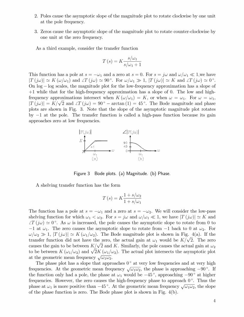
As a third example, consider the transfer function
T (s) = Ks/ω1
s/ω1 + 1
This function has a pole at s = −ω1 and a zero at s = 0. For s = jω and ω/ω1 1,we have|T (jω)| K (ω/ω1) and T (jω) 90 . For ω/ω1 1, |T (jω)| K and T (jω) 0 .On log− log scales, the magnitude plot for the low-frequency approximation has a slope of+1 while that for the high-frequency approximation has a slope of 0. The low and high-frequency approximations intersect when K (ω/ω1) = K, or when ω = ω1. For ω = ω1,|T (jω)| = K/
√2 and T (jω) = 90 − arctan (1) = 45 . The Bode magnitude and phase
plots are shown in Fig. 3. Note that the slope of the asymptotic magnitude plot rotatesby −1 at the pole. The transfer function is called a high-pass function because its gainapproaches zero at low frequencies.
Figure 3 Bode plots. (a) Magnitude. (b) Phase.
A shelving transfer function has the form
T (s) = K1 + s/ω21 + s/ω1
The function has a pole at s = −ω1 and a zero at s = −ω2. We will consider the low-passshelving function for which ω1 < ω2. For s = jω and ω/ω1 1, we have |T (jω)| K and T (jω) 0 . As ω is increased, the pole causes the asymptotic slope to rotate from 0 to−1 at ω1. The zero causes the asymptotic slope to rotate from −1 back to 0 at ω2. Forω/ω2 1, |T (jω)| K (ω1/ω2). The Bode magnitude plot is shown in Fig. 4(a). If thetransfer function did not have the zero, the actual gain at ω1 would be K/
√2. The zero
causes the gain to be between K/√2 and K. Similarly, the pole causes the actual gain at ω2
to be between K (ω1/ω2) and√2K (ω1/ω2). The actual plot intersects the asymptotic plot
at the geometric mean frequency√ω1ω2.
The phase plot has a slope that approaches 0 at very low frequencies and at very highfrequencies. At the geometric mean frequency
√ω1ω2, the phase is approaching −90 . If
the function only had a pole, the phase at ω1 would be −45 , approaching −90 at higherfrequencies. However, the zero causes the high-frequency phase to approach 0 . Thus thephase at ω1 is more positive than −45 . At the geometric mean frequency
√ω1ω2, the slope
of the phase function is zero. The Bode phase plot is shown in Fig. 4(b).
4

Figure 4 Bode plots. (a) Magnitude. (b) Phase.
Classes of Filter FunctionsThe filters considered in this experiment can be divided into four classes. These are low-pass,high-pass, band-pass and band-reject. Although it is impossible to realize an ideal filter, thecharacteristics of the four classes of filters are simplest to describe for ideal filters. Anideal low-pass filter has a cutoff frequency below which the gain is independent of frequencyand above which the gain is zero. Fig. 5(a) illustrates the magnitude response of an ideallow-pass filter having a gain K. The responses of two physically realizable filters are alsoshown. An ideal high-pass filter has a cutoff frequency above which the gain is constant andbelow which the gain is zero. The magnitude responses of an ideal high-pass filter and twophysically realizable filters are illustrated in Fig. 5(b). An ideal band-pass filter has twocutoff frequencies between which the gain is constant and zero elsewhere. The magnituderesponses of an ideal band-pass filter and two physically realizable filters are illustrated inFig. 5(c). An ideal band-reject filter has two cutoff frequencies between which the gain iszero and constant elsewhere. The magnitude responses of an ideal band-reject filter and twophysically realizable filters are illustrated in Fig. 5(d).
Figure 5 (a) Low pass. (b) High pass. (c) Band pass. (d) Band reject.
Low-pass filters are used in applications where it is desired to remove the high-frequencycontent of a signal. For example, aliasing distortion can occur if a signal is applied to theinput of an analog-to-digital converter that has a frequency higher than one-half the samplingfrequency of the converter. A low-pass filter might be used to limit the bandwidth of thesignal. Similarly, a high-pass filter is used in applications where it is desired to remove thelow-frequency content of a signal. For example, the tweeter driver in a loudspeaker can be
5
damaged by low frequencies signals. To prevent this, a high-pass filter called a crossovernetwork must be connected to the tweeter.
A band-pass filter is used in applications where it is desired to pass only the frequenciesin a band. For example, to detect a low level tone that is buried in noise, a band-passfilter might be used to pass the tone and reject the noise. A band-reject filter is used inapplications where it is desired to reject a particular frequency or band of frequencies. Forexample, a 60 Hz hum induced in the amplifier of a public address system might be filteredout with a band-pass filter.
Frequency TransformationsFilter transfer functions are normally derived as low-pass functions. Frequency transforma-tions are then used to transform the low-pass functions into either high-pass, band-pass,or band-reject transfer functions. For a low-pass filter, let the normalized frequency p bedefined by
p =s
ωc
where ωc is a normalization frequency. For the case of low-pass and high-pass filters, ωcis the called the cutoff frequency of the filter. Depending on the type of filter, it is notnecessarily the −3 dB cutoff frequency. To distinguish between the two in the following, ω3is used to denote the −3 dB cutoff frequency. In the case of a band-pass filter, ωc is thecenter frequency of the band-pass response. In the case of a band-reject filter, ωc is thecenter frequency of the band-reject response.
The frequency transformations are defined as follows:
Low-Pass to High-Pass p → 1
p
Low-Pass to Band-Pass p → B
(p+
1
p
)
Low-Pass to Band-Reject p → B−1
(p+
1
p
)−1
where the arrow is read “is replaced by”. The parameter B determines the −3 dB bandwidthof the band-pass and band-reject functions.
Transformations of First-Order Functions
As an example, consider the first-order low-pass filter function
TLP (s) =1
1 + s/aωc
where a is a positive constant. The function TLP (p) is given by
TLP (p) =1
1 + p/a
The high-pass, band-pass, and band-reject transfer functions are given by
High-Pass THP (p) =1
1 + 1/ap=
ap
1 + ap
Band-Pass TBP (p) =1
1 +B (p+ 1/p) /a=
(a/B) p
p2 + (a/B) p+ 1
6

Band-Reject TBR (p) =1
1 +B−1 (p+ 1/p)−1 /a=
p2 + 1
p2 + (1/aB) p + 1
Note that the order of the transfer function is doubled for the band-pass and band-rejecttransformations.
Transformations of Second-Order Functions
Consider the second-order low-pass function
TLP (s) =1
(s/aωc)2 + (1/b) (s/aωc) + 1
where a and b are positive constants. The function TLP (p) is given by
TLP (p) =1
(p/a)2 + (1/b) (p/a) + 1
The high-pass, band-pass, and band-reject transfer functions are given by
High Pass THP (p) =1
(1/ap)2 + (1/b) (1/ap) + 1=
(ap)2
(ap)2 + (1/b) (ap) + 1
Band Pass TBP (p) =1
[B (p+ 1/p) /a]2 + (1/b) [B (p+ 1/p) /a] + 1
=(a2/B2) p2
p4 + (a/bB) p3 + (a2/B2 + 2) p2 + (a/bB) p+ 1
Band Reject TBR (p) =1
[B−1 (p+ 1/p)−1 /a
]2+ (1/b)
[B−1 (p+ 1/p)−1 /a
]+ 1
=(p2 + 1)
2
p4 + (1/abB) p3 + (1/a2B2 + 2) p2 + (1/abB) p+ 1
Butterworth Filter Transfer FunctionsThe Butterworth Approximation
The general form of a nth-order low-pass filter transfer function having no zeros can bewritten
TLP (s) = K1
1 + c1 (s/ωc) + c2 (s/ωc)2 + · · ·+ cn (s/ωc)
n
where K is the dc gain constant, ωc is a normalization frequency, and the ci are positiveconstants. The magnitude squared function is obtained by setting s = jω and solving for|TLP (jω)|2. This function contains only even powers of ω and is of the form
|TLP (jω)|2 = K2 1
1 + C1 (ω/ωc)2 + C2 (ω/ωc)
4 + · · ·+ Cn (ω/ωc)2n
where the Ci are positive constants which are related to the ci.For the Butterworth filter, the constants Ci are chosen so that |TLP (jω)|2 approximates
the magnitude squared function of an ideal low-pass filter in the maximally flat sense. Themagnitude squared function for the ideal filter is defined by
|TLP (jω)|2 = K2 for ω ≤ ωc
= 0 for ω > ωc
7

To obtain the maximally-flat approximation, the Ci are chosen to make as many derivativesas possible of |TLP (jω)|2 equal to zero at ω = 0. If the derivative of a function is zero, thederivative of the reciprocal of the function is also zero. It follows that the maximally flatcondition can be imposed by solving for the constants Ci which make as many derivatives as
possible of[|TLP (jω)|2
]−1equal to zero at ω = 0. Because the denominator polynomial of
|TLP (jω)|2 is an even function, all odd-order derivatives are already zero at ω = 0. For thesecond derivative to be zero, we must have C1 = 0. For the fourth derivative to be zero, wemust have C2 = 0. This procedure is repeated to obtain Ci = 0 for all i. However, we cannotset Cn = 0 because this would make the approximating function independent of frequency.Therefore, we set Ci = 0 for all 1 ≤ i ≤ n− 1 to obtain
|TLP (jω)|2 = K2 1
1 + Cn (ω/ωc)2n
The first 2n− 1 derivatives of this function are zero at ω = 0.It is standard to choose Cn to make |TLP (jωc)|2 = K2/2. This forces the−3 dB frequency
ω3 to be equal to the normalization frequency ωc. This condition requires Cn = 1. Thus themagnitude squared function of the nth-order Butterworth low-pass filter becomes
|TLP (jω)|2 = K2 1
1 + (ω/ωc)2n
Figure 6 shows example plots of |TLP (jω)| for 1 ≤ n ≤ 5 for the Butterworth low-passfilter. The plots assume that K = 1. The horizontal axis is the normalized radian frequencyv = ω/ωc. Each function has the value 1 at v = 0, the value 0.5 at v = 1, and approaches 0as v →∞. As the order n increases, the width of the flat region in the passband is extendedand the filter exhibits a sharper cutoff. The response characteristic is called maximally flatbecause there are no ripples in the passband response.
2.521.510.50
1
0.75
0.5
0.25
0
x
y
x
y
Figure 6 Plots of the Butterworth magnitude response for 1 ≤ n ≤ 5.
To illustrate how the maximally flat condition is applied to a specific filter transferfunction, consider the third-order low-pass function
TLP (s) = K1
1 + c1 (s/ωc) + c2 (s/ωc)2 + c3 (s/ωc)
3
The magnitude squared function is given by
|TLP (jω)|2 = K2 1
1 + (c21 − 2c2) (ω/ωc)2 + (c22 − 2c1c3) (ω/ωc)4 + c23 (ω/ωc)6
8

For this to be maximally flat with a −3 dB cutoff frequency of ωc, we must have
c21 − 2c2 = 0
c22 − 2c1c3 = 0
c3 = 1
Solution for c1 and c2 yields c1 = c2 = 2. Thus the Butterworth third-order low-pass transferfunction is
TLP (s) = K1
1 + 2 (s/ωc) + 2 (s/ωc)2 + (s/ωc)
3
= K1
1 + (s/ωc)× 1
1 + (s/ωc) + (s/ωc)2
The maximally flat filters are called Butterworth filters after S. Butterworth who de-scribed the procedure for deriving the transfer functions in his 1930 paper “On the Theoryof Filter Amplifiers” which was published in Wireless Engineer. The resulting denomina-tor polynomials for TLP (s) are called Butterworth polynomials. The first six Butterworthpolynomials in factored form are
b1 (x) = (x+ 1)
b2 (x) =(x2 + 1.4142x+ 1
)
b3 (x) = (x+ 1)(x2 + x+ 1
)
b4 (x) =(x2 + 0.7654x+ 1
) (x2 + 1.8478x+ 1
)
b5 (x) = (x+ 1)(x2 + 0.6180x+ 1
) (x2 + 1.6180x+ 1
)
b6 (x) =(x2 + 0.5176x+ 1
) (x2 + 1.4142x+ 1
) (x2 + 1.9319x+ 1
)
Even-Order Butterworth Filters
For an even-order Butterworth low-pass filter of order n, the transfer function can be writtenin the product form
TLP (s) =
n/2∏
i−1
1
(s/ωc)2 + (1/bi) (s/ωc) + 1
The constants bi are given by
bi =1
2 sin θi
where the θi are given by
θi =2i− 1
n× 90 for 1 ≤ i ≤ n
2
Example 1 Solve for the transfer functions of the second-order Butterworth low-pass and
high-pass filters.
Solution. For n = 2, there is only one second-order transfer function. The calculationsare summarized as follows:
i θi bi1 45 1/
√2
9

The low-pass transfer function is given by
T (s) = K1
(s/ωc)2 +
√2 (s/ωc) + 1
The high-pass transfer function is obtained by replacing s/ωc with ωc/s to obtain
T (s) = K1
(ωc/s)2 +
√2 (ωc/s) + 1
= K(s/ωc)
2
(s/ωc)2 +
√2 (s/ωc) + 1
Odd-Order Butterworth Filters
For an odd-order Butterworth low-pass filter of order n, the transfer function can be writtenin the product form
TLP (s) =1
s/ωc + 1×(n−1)/2∏
i=1
1
(s/ωc)2 + (1/bi) (s/ωc) + 1
The constants bi are given by
bi =1
2 sin θi
where the θi are given by
θi =2i− 1
n× 90 for 1 ≤ i ≤ n− 1
2
Example 2 Solve for the transfer functions of the third-order Butterworth low-pass and
high-pass filters.
Solution. For n = 3, each transfer function contains one first-order polynomial and onesecond-order polynomial. The calculations for the second-order polynomial are summarizedas follows:
i θi bi1 30 1
The low-pass transfer function is given by
TLP (s) =1
(s/ωc) + 1× 1
(s/ωc)2 + (s/ωc) + 1
The high-pass transfer function is obtained by replacing s/ωc with ωc/s to obtain
THP (s) =1
(ωc/s) + 1× 1
(ωc/s)2 + (ωc/s) + 1
=(s/ωc)
(s/ωc) + 1× (s/ωc)
2
(s/ωc)2 + (s/ωc) + 1
10

The Cutoff Frequency
For the Butterworth low-pass and high-pass filter functions, the cutoff frequency ωc is thefrequency at which the magnitude-squared function is down by a factor of 1/2. This is the−3 dB frequency ω3. For the band-pass and band-reject filter functions, the cutoff frequencyωc is the so-called center frequency. There are two frequencies, one on each side of ωc, atwhich the magnitude-squared function is down by a factor of 1/2. These are the two −3 dBfrequencies. Let these be denoted by ωc1 and ωc2. If these are specified, the center frequencyωc and the parameter B in the frequency transformations are given by
ωc =√ωc1ωc2 B =
ωcωc2 − ωc1
Chebyshev Filter Transfer FunctionsThe Chebyshev Approximation
In 1899, the Russian mathematician P. L. Chebyshev (also written Tschebyscheff, Tchebysh-eff, or Tchebicheff) described a set of polynomials tn (x) which have the feature that theyripple between the peak values of +1 and −1 for −1 ≤ x ≤ +1. His polynomials are widelyused in filter approximations for frequencies that span the audio band to the microwaveband. The first six Chebyshev polynomials are
t1 (x) = x
t2 (x) = 2x2 − 1t3 (x) = 4x3 − 3xt4 (x) = 8x4 − 8x2 + 1t5 (x) = 16x5 − 20x3 + 5xt6 (x) = 32x6 − 48x4 + 18x2 − 1
Figure 7 shows the plots of the first four of these polynomials over the range −2 ≤ x ≤ +2.
2.51.250-1.25-2.5
2
1
0
-1
-2
x
y
x
y
Figure 7 Plots of Chebyshev polynomials for 1 ≤ n ≤ 4.
The Chebyshev approximation to the magnitude squared function of a low-pass filter isgiven by
|TLP (jω)|2 = K2 1 + ε2t2n (0)
1 + ε2t2n (ω/ωc)
where K is the dc gain constant and ε is a parameter which determines the amount of ripplein the approximation. For ω = 0, it follows that |TLP (jω)|2 = K2. For n odd, t2n (0) = 0 sothat the numerator in |TLP (jω)|2 has the value 1. For 0 ≤ ω ≤ ωc, the denominator ripples
11

between the values 1 and 1 + ε2. This causes |TLP (jω)|2 to ripple between the values K2
and K2/ (1 + ε2). At ω = ωc, it has the value K2/ (1 + ε2). For ω > ωc, |TLP (jω)|2 → 0.For n even, t2n (0) = 1 so that the numerator in |TLP (jω)|2 has the value 1 + ε2. For
0 ≤ ω ≤ ωc, the denominator ripples between the values 1 and 1+ε2. This causes |TLP (jω)|2to ripple between the values K2 and K2 (1 + ε2). At ω = ωc, it has the value K2. For ω > ωc,|TLP (jω)|2 → 0. The major difference between the even and odd order approximations isthat the odd-order functions ripple down from the zero frequency value whereas the even-order functions ripple up.
Figure 8 shows example plots of |TLP (jω)| for the 0.5 dB ripple 4th and 5th order filters.The plots assume that K = 1. The horizontal axis is the normalized radian frequencyv = ω/ωc. The figure shows the 4th order approximation rippling up by 0.5 dB from itszero frequency value. The 5th order approximation ripples down by 0.5 dB from its zerofrequency. Compared to the Butterworth filters, the Chebyshev filters exhibit a sharpercutoff at the expense of ripple in the passband. The more the ripple, the sharper the cutoff.
0
0.2
0.4
0.6
0.8
1
1.2
y
0.5 1 1.5 2 2.5v
Figure 8 Plots of the magnitude responses of the 0.5 dB ripple 4th and 5th order Chebyshevfilters.
The dB Ripple
The dB ripple for a Chebyshev filter is the peak-to-peak passband ripple in the Bode mag-nitude plot of the filter response. The dB ripple determines the parameter ε as follows:
dB ripple = 10 log(1 + ε2
)
This can be solved for ε to obtain
ε =√10dB/10 − 1
The Cutoff Frequency
Unlike the Butterworth filter, the cutoff frequency for the Chebyshev filter is not the fre-quency at which the response is down by 3 dB. The cutoff frequency is the frequency atwhich the Bode magnitude plot leaves the “equal-ripple box” in the filter passband. For theeven-order low-pass filters, the gain at the cutoff frequency is equal to the zero frequencygain. For the odd-order low-pass filters, the gain at the cutoff frequency is down from thezero frequency gain by an amount equal to the dB ripple.
For the nth-order Chebyshev low-pass filter, the −3 dB frequency ω3 can be related tothe cutoff frequency ωc by setting |F (jω)|2 = K2/2. The value of ω which satisfies thisequation is the −3 dB frequency ω3. If we let x = ω/ωc, this leads to the equation
tn (x)−√1
ε2+ 2t2n (0) = 0
12
The positive value of x which satisfies this equation is the desired solution. If the −3 dBfrequency for the low-pass and high-pass filters is specified, the required cutoff frequency ωcis given by
Low Pass (of order n) ωc =ω3x
High Pass (of order n) ωc = xω3
For the band-pass and band-reject filter functions, the cutoff frequency ωc is the so-calledcenter frequency. There are two frequencies, one on each side of ωc, at which the magnitude-squared function is down by a factor of 1/2. These are the two −3 dB frequencies. Let thesebe denoted by ωc1 and ωc2. If these are specified, the center frequency ωc and the parameterB in the frequency transformations are given by
ω2 − ωc1ωc2ωωc
=ωc1 − ωc2
ωc=
ωc2 − ωc1ωc
Band Pass (of order 2n) ωc =√ωc1ωc2 B =
xωcωc2 − ωc1
Band Reject (of order 2n) ωc =√ωc1ωc2 B =
ωc/x
ωc2 − ωc1where ω3 is the −3 dB radian frequency. For any x, there are two values of ω3 which satisfythe band-pass and band-reject relations. Denote these by ωa and ωb. The geometric meanof these two frequencies must equal ωc, i.e. ωc =
√ωaωb. In a design from specifications,
the −3 dB frequencies might be specified for the band-pass and band-reject filters. In thiscase, the required values for the center frequency and the parameter B in the frequencytransformation can be solved for.
Example 3 An 4th-order 0.5 dB ripple low-pass filter is to have the −3 dB cutoff frequencyf3 = 10 kHz. Calculate the required cutoff frequency fc.
Solution. The parameter ε has the value ε =√100.5/10 − 1 = 0.34931. We must solve for
the positive real root of the equation
8x4 − 8x2 + 1−√
1
0.349312+ 2 = 0
The desired root is x = 1.1063. It follows that the required cutoff frequency is fc = f3/x =9.039 kHz.
Example 4 An 4th-order 0.5 dB ripple high-pass filter is to have the −3 dB cutoff frequencyf3 = 10 kHz. Calculate the required cutoff frequency fc.
Solution. The value of x from the low-pass example gives fc = xf3 = 11.063 kHz.
Example 5 An 8th-order 0.5 dB ripple band-pass filter is to have a center frequency fc =10 kHz and a bandwidth fc2 − fc1 = 2kHz. Note that the transfer function is obtained fromthat for the 4th-order LPF so that the band-pass filter is 8th order. Calculate the value of Bin the low-pass to band-pass transformation.
Solution. The value of x from the low-pass example gives B = xfc/ (fc2 − fc1) = 5.532.
Example 6 An 8th-order 0.5 dB ripple band-reject filter is to have a center frequency fc =10 kHz and a bandwidth fc2 − fc1 = 2kHz. Note that the transfer function is obtained fromthat for the 4th-order LPF so that the band-reject filter is 8th order.. Calculate the value ofB in the low-pass to band-pass transformation.
Solution. The value of x from the low-pass example gives B = (fcx−1) / (fc2 − fc1) = 4.52.
13

The Parameter hTo write the Chebyshev transfer functions, the parameter h is required. Given the order nand the ripple parameter ε, h is defined by
h = tanh
(1
nsinh−1
1
ε
)
Even-Order Chebyshev Filters
For an even-order Chebyshev low-pass filter of order n, the transfer function can be writtenin the product form
TLP (s) =
n/2∏
i=1
1
(s/aiωc)2 + (1/bi) (s/aiωc) + 1
The constants ai and bi are given by
ai =
(1
1− h2− sin2 θi
)1/2for 1 ≤ i ≤ n/2
bi =1
2
(1 +
1
h2 tan2 θi
)1/2for 1 ≤ i ≤ n/2
where the θi are given by
θi =2i− 1
n× 90 for 1 ≤ i ≤ n/2
Example 7 Solve for the transfer function of the 0.5 dB ripple fourth-order Chebyshev low-pass and high-pass filters.
Solution. The parameters ε and h are given by
ε =(100.5/10 − 1
)1/2= 0.3493
h = tanh
(1
4sinh−1
1
0.3493
)= 0.4166
For n = 4, there are two second-order polynomials in each transfer function. The calculationsare summarized as follows:
i θi ai bi1 22.5 1.0313 2.94062 67.5 0.59703 0.7051
The low-pass transfer function is given by
TLP (s) =1
(s/1.0313ωc)2 + (1/2.9406) (s/1.0313ωc) + 1
× 1
(s/0.59703ωc)2 + (1/0.7051) (s/0.59703ωc) + 1
14

The high-pass transfer function is obtained by replacing s/ωc with ωc/s to obtain
THP (s) =1
(ωc/1.0313s)2 + (1/2.9406) (ωc/1.0313s) + 1
× 1
(ωc/0.59703s)2 + (1/0.7051) (ωc/0.59703s) + 1
=(1.0313s/ωc)
2
(1.0313s/ωc)2 + (1/2.9406) (1.0313s/ωc) + 1
× (0.59703s/ωc)2
(0.59703s/ωc)2 + (1/0.7051) (0.59703s/ωc) + 1
Odd-Order Chebyshev Filters
For an odd-order Chebyshev low-pass filter of order n, the transfer function can be writtenin the form
TLP (s) =1
s/a(n+1)/2ωc + 1×(n−1)/2∏
i=1
1
(s/aiωc)2 + (1/bi) (s/aiωc) + 1
The constants ai and bi are given by
a(n+1)/2 =h√1− h2
for i = (n+ 1) /2
ai =
(1
1− h2− sin2 θi
)1/2for 1 ≤ i ≤ (n− 1) /2
bi =1
2
(1 +
1
h2 tan2 θi
)1/2for 1 ≤ i ≤ (n− 1) /2
where the θi are given by
θi =2i− 1
n× 90 for 1 ≤ i ≤ (n− 1) /2
Example 8 Solve for the transfer function for the 1 dB ripple third-order Chebyshev low-pass and high-pass filters.
Solution. The parameters ε and h are given by
ε =(101/10 − 1
)1/2= 0.5088
h = tanh
(1
3sinh−1
1
0.5088
)= 0.4430
For n = 3, each transfer function contains one second-order polynomial and one first-orderpolynomial. The calculations are summarized as follows:
i θi ai bi1 30 0.9971 2.01772 – 0.4942 –
15

The low-pass transfer function is given by
TLP (s) =1
(s/0.4942ωc) + 1× 1
(s/0.9971ωc)2 + (1/2.0177) (s/0.9971ωc) + 1
The high-pass function is obtained by replacing s/ωc with ωc/s to obtain
THP (s) =1
(ωc/0.4942s) + 1× 1
(ωc/0.9971s)2 + (1/2.0177) (ωc/0.9971s) + 1
=(0.4942s/ωc)
(0.4942s/ωc) + 1× (0.9971s/ωc)
2
(0.9971s/ωc)2 + (1/2.0177) (0.9971s/ωc) + 1
Elliptic Filter Transfer FunctionsThe elliptic filter is also known as the Cauer-Chebyshev filter. It is a filter which exhibitsequal ripple in the passband and in the stop band. It can be designed to have a much steeperroll off than the Chebyshev filter. The approximation to the magnitude squared function ofthe elliptic low-pass filter is of the form
|TLP (jω)|2 = K2 1 + ε2R2n (0)
1 + ε2R2n (ω/ωc)
where K is the dc gain constant, ε determines the dB ripple, and Rn (ω/ωc) is the rationalChebychev function. This function has the form
Rn (x) =
n/2∏
i=1
q2i1− (x/qi)2
1− (qix)2for n even
= x
(n−1)/2∏
i=1
q2i1− (x/qi)2
1− (qix)2for n odd
where 0 < qi < 1. From this definition, it follows that Rn (x) satisfies the following properties:
Rn
(1
x
)=
1
Rn (x)Rn (qi) = 0 Rn
(1
qi
)=∞
Rn (0) =
n/2∏
i=1
q2i for n even
= 0 for n odd
Rn (1) = (−1)n/2 for n even
= (−1)(n−1)/2 for n odd
Rn (∞) =
n/2∏
i=1
(−1)ia2i
for n even
= ∞ for n odd
16

It is beyond the scope of this treatment to describe how the qi are specified. For n even,the transfer function can be put into the form
TLP (s) =
n/2∏
i=1
(s/ciωc)2 + 1
(s/aiωc)2 + (1/bi) (s/aiωc) + 1
For n odd, the form is
TLP (s) =1
s/a(n+1)/2ωc + 1×(n−1)/2∏
i=1
(s/ciωc)2 + 1
(s/aiωc)2 + (1/bi) (s/aiωc) + 1
These differ from the forms for the Chebyshev filter by the presence of zeros on the jω axis.That is, TLP (jω) = 0 for ω = ciωc.
Figure 9 shows the plot of |TLP (jv)| for a 4th-order elliptic filter, where v = ω/ωc isthe normalized radian frequency. The filter has a dB ripple of 0.5 dB for v ≤ 1. Like theChebyshev filters, the gain ripples up from its dc value for the even order filter. There aretwo zeros in the response, one at v = 1.59 and the other at v = 3.48. For v > 1.5, the gainripples between 0 and 0.0153. As v becomes large, the gain approaches the value 0.0153which is 36.3 dB down from the dc value. Odd order elliptic filters have the property thatthe gain ripples down from the dc value and approaches 0 as v becomes large.
0
0.2
0.4
0.6
0.8
1
y
2 4v
Figure 9 Magnitude response versus normalized frequency for the example elliptic filter.
The passband for the elliptic filter is the band defined by ω ≤ ωc. Like the Chebyshevfilters, the dB ripple is defined in this band. The even-order filters ripple up from the dc gain,whereas the odd-order filters ripple down. At ω = ωc, the gain of an even-order filter is equalto the dc gain, whereas the gain of an odd-order filter is down by an amount equal to the dBripple. For ω > ωc, the gain decreases rapidly and is equal to zero at the zero frequencies ofthe transfer function. Between adjacent zeros, the gain peaks up in an equal ripple fashion,i.e. with equal values at the peaks. Let the gain at the peaks between adjacent zeros have adB level that is down from the dc gain by Amin dB. The stop band frequency ωs is defined asthe frequency between the cutoff frequency ωc and the first zero frequency at which the gainis down by Amin dB. For ω > ωs, the gain is down from the dc level by Amin dB or more.
The three parameters which define the alignment of an elliptic filter are the dB ripple inthe passband, the ratio ωs/ωc of the stop band frequency to the cutoff frequency, and theminimum dB attenuation Amin in the stop band. The tables below give the values of the ai,bi, and ci in the elliptic transfer functions for 0.5 dB ripple filters having ωs/ωc values of 1.5,2.0, and 3.0 for orders n = 2 through n = 5.
17
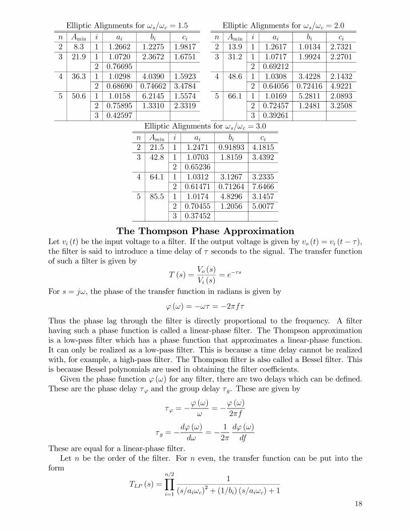
Elliptic Alignments for ωs/ωc = 1.5
n Amin i ai bi ci2 8.3 1 1.2662 1.2275 1.98173 21.9 1 1.0720 2.3672 1.6751
2 0.766954 36.3 1 1.0298 4.0390 1.5923
2 0.68690 0.74662 3.47845 50.6 1 1.0158 6.2145 1.5574
2 0.75895 1.3310 2.33193 0.42597
Elliptic Alignments for ωs/ωc = 2.0
n Amin i ai bi ci2 13.9 1 1.2617 1.0134 2.73213 31.2 1 1.0717 1.9924 2.2701
2 0.692124 48.6 1 1.0308 3.4228 2.1432
2 0.64056 0.72416 4.92215 66.1 1 1.0169 5.2811 2.0893
2 0.72457 1.2481 3.25083 0.39261
Elliptic Alignments for ωs/ωc = 3.0
n Amin i ai bi ci2 21.5 1 1.2471 0.91893 4.18153 42.8 1 1.0703 1.8159 3.4392
2 0.652364 64.1 1 1.0312 3.1267 3.2335
2 0.61471 0.71264 7.64665 85.5 1 1.0174 4.8296 3.1457
2 0.70455 1.2056 5.00773 0.37452
The Thompson Phase ApproximationLet vi (t) be the input voltage to a filter. If the output voltage is given by vo (t) = vi (t− τ ),the filter is said to introduce a time delay of τ seconds to the signal. The transfer functionof such a filter is given by
T (s) =Vo (s)
Vi (s)= e−τs
For s = jω, the phase of the transfer function in radians is given by
ϕ (ω) = −ωτ = −2πfτThus the phase lag through the filter is directly proportional to the frequency. A filterhaving such a phase function is called a linear-phase filter. The Thompson approximationis a low-pass filter which has a phase function that approximates a linear-phase function.It can only be realized as a low-pass filter. This is because a time delay cannot be realizedwith, for example, a high-pass filter. The Thompson filter is also called a Bessel filter. Thisis because Bessel polynomials are used in obtaining the filter coefficients.
Given the phase function ϕ (ω) for any filter, there are two delays which can be defined.These are the phase delay τϕ and the group delay τ g. These are given by
τϕ = −ϕ (ω)
ω= −ϕ (ω)
2πf
τ g = −dϕ (ω)
dω= − 1
2π
dϕ (ω)
df
These are equal for a linear-phase filter.Let n be the order of the filter. For n even, the transfer function can be put into the
form
TLP (s) =
n/2∏
i=1
1
(s/aiωc)2 + (1/bi) (s/aiωc) + 1
18

For n odd, the form is
TLP (s) =1
s/a(n+1)/2ωc + 1×(n−1)/2∏
i=1
1
(s/aiωc)2 + (1/bi) (s/aiωc) + 1
where the time delay of the filter is given by τ = 1/ωc. It is beyond the scope of the treatmenthere to describe how the ai and bi are obtained. The tables below give the values for n = 1to n = 6. Also given is the ratio of the −3 dB frequency f3 to the cutoff frequency fc.
Thompson Alignments for 1 ≤ n ≤ 4n f3/fc i ai bi1 1 1 1.02 1.3617 1 1.7321 0.577353 1.7557 1 2.5415 0.69105
2 2.32224 2.1139 1 3.0233 0.52193
2 3.3894 0.80554
Thompson Alignments for 5 ≤ n ≤ 6n f3/fc i ai bi5 2.4274 1 3.7779 0.56354
2 4.2610 0.916483 3.64674
6 2.8516 1 4.3360 0.510322 4.5665 0.611193 5.1492 1.0233
Figure 10 shows the plot of |T (j2πf)| as a function of frequency for the 4th-order Thomp-son filter for the case ωc = 1 rad/s. This choice gives a delay of 1 second. The −3 dBfrequency of the filter is f3 = 2.1139ω0/2π = 0.3364Hz. If the −3 dB frequency is multipliedby a constant, the delay time is divided by that constant. Fig. 11 shows the phase responseof the filter. The phase delay is shown plotted in Fig. 12. It can be seen from this figurethat the delay is approximately equal to 1 second up to the −3 dB frequency of the filter.
0
0.2
0.4
0.6
0.8
1
y
0.2 0.4 0.6 0.8 1 1.2 1.4f
Figure 10 Plot of |T (j2πf)| versus f .
Second-Order Filter TopologiesSallen-Key Low-Pass Filter
Figure 13 shows the circuit diagram of the second-order Sallen-Key low-pass filter. Thevoltage-gain transfer function is given by
VoVi= K
1
(s/ω0)2 + (1/Q) (s/ω0) + 1
where K is the dc gain constant, ω0 is the radian resonance frequency, and Q is the qualityfactor. These are given by
K = 1 +R4
R3
19

-300
-250
-200
-150
-100
-50
0
y
0.2 0.4 0.6 0.8 1 1.2 1.4f
Figure 11 Plot of the phase in degrees of T (j2πf) versus f .
0.6
0.7
0.8
0.9
1
y
0.2 0.4 0.6 0.8 1 1.2 1.4f
Figure 12 Plot of the phase delay in seconds of T (j2πf) versus f .
20

ω0 =1√
R1R2C1C2
Q =
√R1R2C1C2
(1−K)R1C1 + (R1 +R2)C2
Figure 13 Second-order Sallen-Key low-pass filter.
Special Case 1
Let K = 1 (R4 a short and R3 an open). If R1, R2, ω0, and Q are specified, C1 and C2 aregiven by
C1 =Q
ω0
(1
R1+1
R2
)
C2 =1
Qω0 (R1 +R2)
The filter is often realized with R1 = R2.
Special Case 2
Capacitor values are often difficult to obtain. It is possible to specify C1 and C2 and calculatethe resistors. Let K = 1 (R4 a short and R3 an open). If C1, C2, ω0, and Q are specified,R1 and R2 are given by
R1, R2 =1
2Qω0C2
[
1±√1− 4Q2
C2C1
]
Any value for the ratio C2/C1 can be chosen provided 4Q2C2/C1 ≤ 1. Note that the valuesfor R1 and R2 are interchangeable.
Example 9 Design a unity-gain second-order Sallen-Key low-pass filter with f0 = 1kHzand Q = 1/
√2.
Solution. Let C1 = 0.1µF and C2 = 0.022µF. R1 and R2 are given by
R1, R2 =
√2
2× 2π1000× 0.022× 10−6
[
1±√
1− 4× 12× 0.22
]
= 1.29 kΩ and 8.94 kΩ
Either value may be assigned to R1. The other value is then assigned to R2.
21

Special Case 3
Let R1 = R2 = R and C1 = C2 = C. If C, ω0, and Q are specified, R and K are given by
R =1
ω0C
K = 3− 1
Q
Infinite-Gain Multi-Feedback Low-Pass Filter
Figure 14 shows the circuit diagram of the second-order infinite-gain multi-feedback low-passfilter. The voltage-gain transfer function is given by
VoVi= −K 1
(s/ω0)2 + (1/Q) (s/ω0) + 1
where K is the dc gain constant, ω0 is the radian resonance frequency, and Q is the qualityfactor. These are given by
K =R3R1
ω0 =1√
R2R3C1C2
Q =
√R2R3C1/C2
R2 +R3 +R2R3/R1
Figure 14 Second-order infinite gain multi-feedback low-pass filter.
Special Case 1
Let R1 = R2 = R3 so that K = −1. If R, ω0, and Q are specified, C1 and C2 are given by
C1 =Q
ω0
(2
R1+1
R2
)
C2 =1
Qω0 (R1 + 2R2)
The filter is often designed with R1 = R2.
22

Special Case 2
Capacitor values are often difficult to obtain. It is possible to specify C1 and C2 and calculatethe resistors. Let K = −1 (R3 = R1). If C1, C2, ω0, and Q are specified, R1/2 and R2 aregiven by
R1
2, R2 =
1
4Qω0C2
[
1±√1− 8Q2
C2C1
]
Any value for the ratio C2/C1 can be chosen provided 8Q2C2/C1 ≤ 1. Note that the valuesfor R1/2 and R2 are interchangeable.
Example 10 Design a unity-gain second-order infinite-gain multi-feedback low-pass filter
with f0 = 1 kHz and Q = 1/√2.
Solution. Let C1 = 0.1µF and C2 = 0.01µF. R1/2 and R2 are given by
R12, R2 =
√2
4× 2π1000× 0.01× 10−6
[
1±√1− 8× 1
2× 0.1
]
= 1.27 kΩ and 9.99 kΩ
The filter can be designed either with R1 = 2.54 kΩ and R2 = 9.99 kΩ or with R1 = 20 kΩand R2 = 1.27 kΩ.
Second-Order Low-Pass Filter -3dB Cutoff FrequencyThe −3 dB radian cutoff frequency ω3 of the filters in Figures 13 and 14 is given by
ω3 = ω0
(1− 1
2Q2
)+
√(1− 1
2Q2
)2+ 1
1/2
Sallen-Key High-Pass Filter
Figure 15 shows the circuit diagram for the second-order Sallen-Key high-pass filter. Thevoltage-gain transfer function is given by
VoVi= K
(s/ω0)2
(s/ω0)2 + (1/Q) (s/ω0) + 1
where K is the asymptotic high-frequency gain, ω0 is the resonance frequency, and Q is thequality factor. These are given by
K = 1 +R4
R3
ω0 =1√
R1R2C1C2
Q =
√R1R2C1C2
R1 (C1 + C2) + (1−K)R2C2
23

Figure 15 Second-order Sallen-Key high-pass filter.
Special Case 1
Let C1 = C2 = C and K = 1 (RF a short and R3 an open). If C, ω0, and Q are specified,R1 and R2 are given by
R1 =1
2Qω0C
R2 =2Q
ω0C
Special Case 2
Let R1 = R2 = R and C1 = C2 = C. If R, ω0, and Q are specified, C and K are given by
C =1
ω0R
K = 3− 1
Q
Infinite-Gain Multi-Feedback High-Pass Filter
The second-order infinite-gain multi-feedback high-pass filter is not a stable circuit in prac-tice. This is because its input node connects through two series capacitors to the V− node ofthe op amp. At high frequencies, the input node becomes shorted to a virtual ground. Thiscan cause oscillation problems in the source that drives the filter. Therefore, this topologyis not recommended.
Second-Order High-Pass Filter -3dB Cutoff FrequencyThe −3 dB lower radian cutoff frequency ω3 for the circuit in Figure 15 is given by
ω3 = ω0
(1− 1
2Q2
)+
√(1− 1
2Q2
)2+ 1
−1/2
Sallen-Key Band-Pass Filter
Figure 16 shows the circuit diagram of the second-order Sallen-Key band-pass filter. Thevoltage-gain transfer function is given by
VoVi= K
(1/Q) (s/ω0)
(s/ω0)2 + (1/Q) (s/ω0) + 1
24

where K is the gain at resonance, ω0 is the resonance frequency, and Q is the quality factor.These are given by
K =R2
R1 +R2× K0R3C2(R1‖R2) (C1 + C2) +R3C2 [1−K0R1/ (R1 +R2)]
ω0 =1
√(R1‖R2)R3C1C2
Q =
√(R1‖R2)R3C1C2
(R1‖R2) (C1 + C2) +R3C2 [1−K0R1/ (R1 +R2)]
where K0 is the gain from the non-inverting input of the op amp to the output. This is givenby
K0 = 1 +R5
R4
Figure 16 Second-order Sallen-Key band-pass filter.
Special Case
Let R1 = R2 = R3 = R and C1 = C2 = C. If Q, ω0, and C are specified, R, K0 and K aregiven by
R =
√2
ω0CK0 = 4−
1
Q2K = 4Q2 − 1
Infinite-Gain Multi-Feedback Band-Pass Filter
Figure 17 shows the circuit diagram of the second-order infinite-gain multi-feedback band-pass filter. The voltage-gain transfer function is given by
VoVi= −K (1/Q) (s/ω0)
(s/ω0)2 + (1/Q) (s/ω0) + 1
where K is the gain at resonance, ω0 is the resonance frequency, and Q is the quality factor.These are given by
K =R3C1
R1 (C1 + C2)
ω0 =1
√(R1‖R2)R3C1C2
Q =
√R3C1C2/ (R1‖R2)
C1 + C2
25

Figure 17 Second-order infinite gain multi-feedback band-pass filter.
Special Case
Let C1 = C2 = C. For a specified K, ω0, and Q, R1, R2, and R3 are given by
R1 =Q
Kω0CR2 =
R1(2Q2/K)− 1 R3 =
2Q
ω0C
Second-Order Band-Pass Filter Bandwidth
The −3 dB bandwidth ∆ω3 of a second-order band-pass filter is related to the resonancefrequency ω0 and the quality factor Q by
∆ω3 =ω0Q
Let the lower and upper −3 dB cutoff frequencies, respectively, be denoted by ωa and ωb.These frequencies are related to the bandwidth and the quality factor by
∆ω3 = ωb − ωa
ω0 =√ωaωb
A Biquad Filter
A biquadratic transfer function, or biquad for short, is a transfer function that is the ratioof two second-order polynomials. It has the form
TBQ (s) = K(s/ωn)
2 + (1/Qn) (s/ωn) + 1
(s/ωd)2 + (1/Qd) (s/ωd) + 1
where K, ωn, Qn, ωd, and Qd are constants. The function can be thought of as the sum ofthree transfer functions: a low-pass, a band-pass, and a high-pass. For the case Qn → ∞,the zeros are on the jω axis and the transfer function exhibits a notch at ω = ωc, i.e.TBQ (jωn) = 0. Band-reject filters and elliptic filters have biquad terms of this form.
In general, the simplest biquad circuits to realize are the ones which require more thanone op amp. Compared to the single op amp biquads, these circuits can be realized withonly one capacitor value and they are usually easier to tweak. Fig. 18 shows the circuitdiagram of an example three op amp biquad. For this circuit, we can write
Va = −(R4‖
1
Cs
)(ViR3
+VbR
)
Vo = −R(VaR+
ViR2
)
Vb =−1Cs
(VoR+
ViR1
)
26

Figure 18 Biquad filter.
Although these equations look deceptively simple, a lot of algebra is required to solve forVo/Vi. The solution is of the form of TBQ (s) given above. For a specified K, ωd, Qd, ωn, Qn,and C, the design equations for the circuit are
R =1
ωdC
R1 =R
K
R2 =
(ωnωd
)2R1
R3 =ωdR2
ωd/Qd − ωn/Qn
R4 = QdR
Example 11 Design a third-order elliptic low-pass filter having 0.5 dB ripple, a notch in itstransfer function at f = 15, 734Hz, a stop-band attenuation of 21.9 dB, and a stop band tocutoff frequency ratio of fs/fc = 1.5. The gain at dc is to be unity.
Solution. From the fc/fs = 1.5 Elliptic filter table, the transfer function is given by
F (s) =1
s/0.76695ωc + 1× (s/1.6751ωc)
2 + 1
(s/1.0720ωc)2 + (1/2.3672) (s/1.0720ωc) + 1
where ωc is the cutoff frequency. The transfer function has a null at ω = 1.6751ωc. For thenull to be at 15, 734Hz, we have ωc = 2π15734/1.6751 = 59, 017. Thus the transfer functionis
F (s) =1
s/45263 + 1× (s/98859)2 + 1
(s/63266)2 + (1/2.367) (s/63266) + 1
The biquadratic term can be realized with the three op amp biquad. Let C = 1000 pF.
27

The element values are given by
R =1
63266C= 15.81 kΩ
R1 =R
1= 15.81 kΩ
R2 =
(98859
63266
)2R1 = 38.60 kΩ
R3 =63266R2
63266/2.367− 98859/∞ = 2.367R2 = 91.37 kΩ
R4 = 2.367R = 37.42 kΩ
The first-order term can be realized as a passive filter at either the input or the output ofthe biquad. The preferred realization does not require a buffer stage for isolation. One wayof accomplishing this is to divide R1, R2, and R3 each into two series resistors, where theratio of the resistors in each pair is the same. By voltage division, the voltage at the nodewhere the resistors in each pair connect is the same for the three pairs. Thus these threenodes can be connected together. A capacitor to ground from this node then realizes thefirst-order term.
Let the ratio of the resistors in each pair be 0.33/0.67. Divide R1 into series resistorsof values 0.33R1 = 5.217 kΩ and 0.67R1 = 10.59 kΩ. Similarly, divide R2 into resistorsof values 0.33R2 = 12.74 kΩ and 0.67R2 = 25.86 kΩ and divide R3 into resistors of values0.33R3 = 30.15 kΩ and 0.67R3 = 61.21 kΩ. Let the smaller of the resistors in each pairconnect to the Vi node. These three resistors are in parallel in the circuit and can bereplaced with a single resistor of value 5.217‖12.74‖30.15 = 3.297 kΩ. The time constantfor the capacitor which sets the single-pole term in the transfer function is RpC, whereRp = 3.297‖10.59‖25.86‖61.21 = 2.209 kΩ. Thus C = 1/ (45263× 2209) = 0.01µF. Thecompleted circuit is given in Fig. 19. The magnitude response is shown in Fig. 20.
Figure 19 Completed elliptic filter.
28

0
0.2
0.4
0.6
0.8
1
5 10 15 20 25v
Figure 20 Magnitude response versus frequency in kHz.
A Second Biquad Filter
A second biquad filter that has its zeros on the jω axis is shown in Fig. 21. The followingequations can be written for the circuit:
Va = − ViR1C1s
− VoR3C1s
Vb = −R4R5
Vi
Vc =
(VaR2
+ VbC2s
)(R2‖
1
C2s
)Vo =
(1 +
R7R6
)Vc
These equations can be solved for Vo/Vi to obtain
VoVi= −K (s/ωn)
2 + 1
(s/ωd)2 + (1/Qd) (s/ωd) + 1
where
K =R3R1
ωn =
√R5
R1R2R4C1C2
ωd =
√1 +R7/R6R2R3C1C2
Qd =
√(1 +
R7
R6
)R2C2R3C1
Figure 21 A second biquad circuit.
29

Because there are more element values than equations that relate them, values must beassigned to some of the elements before the others can be calculated. Let values for C1, C2,K, R5, and 1 +R7/R6 be specified. The other element values are given by
R1 =1 +R7/R6KQdC1ωd
R2 =Qd
ωdC2R3 = KR1 R4 = K
(ωdωn
)2R5
1 + R7/R6
Third-Order Sallen-Key Filter CircuitsThe filter circuits given in this section consist of a first-order stage in cascade with a second-order stage with no buffer amplifier isolating the two stages. The transfer functions aredifficult to derive.
Low-Pass Filters
Figure 22 Third-order Sallen-Key low-pass filter.
Figure 22 shows the circuit diagram of a third-order unity-gain Sallen-Key low-pass filter.For R1 = R2 = R3 = R, it can be shown that the transfer function for this filter is given by
VoVi=
1
R3C1C2C3s3 + 2R2C1 (C2 + C3) s2 +R (3C1 + C3) s+ 1
For a cutoff frequency ωc, the element values for Butterworth and Chebyshev filters are givenin the following table. The Butterworth filters are 3 dB down at :ωc whereas the Chebyshevfilters are down by an amount equal to the dB ripple.
Alignment R1 R2 R3 C1 C2 C3Butterworth R R R 0.20245/Rωc 3.5465/Rωc 1.3926/Rωc
0.01 dB Chebyshev R R R 0.07130/Rωc 2.5031/Rωc 0.8404/Rωc0.03 dB Chebyshev R R R 0.07736/Rωc 3.3128/Rωc 1.0325/Rωc0.10 dB Chebyshev R R R 0.09691/Rωc 4.7921/Rωc 1.3145/Rωc0.30 dB Chebyshev R R R 0.08582/Rωc 7.4077/Rωc 1.6827/Rωc1.0 dB Chebyshev R R R 0.05872/Rωc 14.784/Rωc 2.3444/Rωc
High-Pass Filters
Figure 23 shows the circuit diagram of a third-order unity-gain Sallen-Key high-pass filter.For C1 = C2 = C3 = C, it can be shown that the transfer function for this filter is given by
VoVi=
R1R2R3C3s3
R1R2R3C3s3 +R2 (R1 + 3R3)C2s2 + 2 (R2 +R3)Cs+ 1
For a cutoff frequency ωc, the element values for Butterworth and Chebyshev filters are givenin the following table. The Butterworth filters are 3 dB down at :ωc whereas the Chebyshevfilters are down by an amount equal to the dB ripple.
30

Figure 23 Third-order Sallen-Key high-pass filter.
Alignment R1 R2 R3 C1 C2 C3Butterworth 4.93949/ωcC 0.28194/ωcC 0.71808/ωcC C C C
0.01 dB Chebyshev 10.9130/ωcC 0.39450/ωcC 1.18991/ωcC C C C0.03 dB Chebyshev 10.09736/ωcC 0.30186/ωcC 0.96852/ωcC C C C0.1 dB Chebyshev 10.3188/ωcC 0.20868/ωcC 0.76075/ωcC C C C0.3 dB Chebyshev 11.65230/ωcC 0.13499/ωcC 0.59428/ωcC C C C1.0 dB Chebyshev 17.0299/ωcC 0.06764/ωcC 0.42655/ωcC C C C
Impedance Transfer FunctionsRC Network
The impedance transfer function for a two-terminal RC network which contains only onecapacitor and is not an open circuit at dc can be written
Z = Rdc1 + τ zs
1 + τps
where Rdc is the dc resistance of the network, τ p is the pole time constant, and τ z is thezero time constant. The pole time constant is the time constant of the network with theterminals open circuited. The zero time constant is the time constant of the network with theterminals short circuited. Figure 24(a) shows the circuit diagram of an example two-terminalRC network. The impedance transfer function can be written by inspection to obtain
Z = R11 +R2Cs
1 + (R1 +R2)Cs
Figure 24 Example RC and RL impedance networks.
RL Network
The impedance transfer function for a two-terminal RL network which contains only oneinductor and is not a short circuit at dc can be written
Z = Rdc1 + τ zs
1 + τps
31

where Rdc is the dc resistance of the network, τ p is the pole time constant, and τ z is thezero time constant. The pole time constant is the time constant of the network with theterminals open circuited. The zero time constant is the time constant of the network with theterminals short circuited. Figure 24(b) shows the circuit diagram of an example two-terminalRL network. The impedance transfer function can be written by inspection to obtain
Z = R1‖R21 + (L/R2) s
1 + [L/ (R1 +R2)] s
Voltage Divider Transfer FunctionsRC Network
The voltage-gain transfer function of a RC voltage-divider network containing only onecapacitor and having a non-zero gain at dc can be written
VoVi= k
1 + τ zs
1 + τ ps
where k is the dc gain (C an open circuit), τ p is the pole time constant, and τ z is the zerotime constant. The pole time constant is the time constant of the network with Vi = 0 andVo open circuited. The zero time constant is the time constant of the network with Vo = 0and Vi open circuited. Figure 25(a) shows the circuit diagram of an example RC network.The voltage-gain transfer function can be written by inspection to obtain
VoVi=
R2 +R3
R1 +R2 +R3× 1 + (R2‖R3)Cs
1 + [(R1 +R2) ‖R3]Cs
Figure 25(b) shows the circuit diagram of a second example RC network. The voltage-gaintransfer function can be written by inspection to obtain
VoVi=
R3R1 +R3
× 1 + (R1 +R2)Cs
1 + [(R1‖R3) +R2]Cs
Figure 25 Example RC voltage divider networks.
High-Pass RC Network
The voltage-gain transfer function of a high-pass RC voltage-divider network containing onlyone capacitor can be written
VoVi= k
τps
1 + τ ps
where k is the infinite frequency gain (C a short circuit) and τ p is the pole time constant.The pole time constant is calculated with Vi = 0 and Vo open circuited. Figure 25(c) shows
32

the circuit diagram of a third example RC network. The voltage-gain transfer function canbe written by inspection to obtain
VoVi=
R2R1 +R2
× (R1 +R2)Cs
1 + (R1 +R2)Cs
RL Network
The voltage-gain transfer function of a RL voltage-divider network containing only oneinductor and having a non-zero gain at dc can be written
VoVi= k
1 + τ zs
1 + τ ps
where k is the zero frequency gain (L a short circuit), τp is the pole time constant, and τ zis the zero time constant. The pole time constant is the time constant of the network withVi = 0 and Vo open circuited. The zero time constant is the time constant of the networkwith Vo = 0 and Vi open circuited. Figure 26(a) shows the circuit diagram of an exampleRL network. The voltage-gain transfer function can be written by inspection to obtain
VoVi=
R2R1 +R2
× 1 + [L/ (R2‖R3)] s1 + (L/ [(R1 +R2) ‖R3]) s
Figure 26(b) shows the circuit diagram of a second example RL network. The voltage-gaintransfer function can be written by inspection to obtain
VoVi=
R3R1 +R3
× 1 + (L/R1) s
1 + (L/ [R1‖ (R2 +R3)]) s
Figure 26 Example RL voltage divider circuits.
High-Pass RL Network
The voltage-gain transfer function of a high-pass RL voltage-divider network containing onlyone inductor can be written
VoVi= k
τps
1 + τ ps
where k is the infinite frequency gain (L an open circuit) and τp is the pole time constant.The pole time constant is calculated with Vi = 0 and Vo open circuited. Figure 26(c) showsthe circuit diagram of a third example RL network. The voltage-gain transfer function canbe written by inspection to obtain
VoVi=
R2R1 +R2
× [L/ (R1‖R2)] s1 + [L/ (R1‖R2)] s
33