dr. p. stamenov
TRANSCRIPT
Semiconductor Devices 2013Semiconductor Devices - 2013
Lecture CoursePart ofPart of
SS Module PY4P03
Dr. P. Stamenov
School of Physics and CRANN, Trinity College,Dublin 2, Ireland,
Hilary Term, TCD04th of Feb ‘13
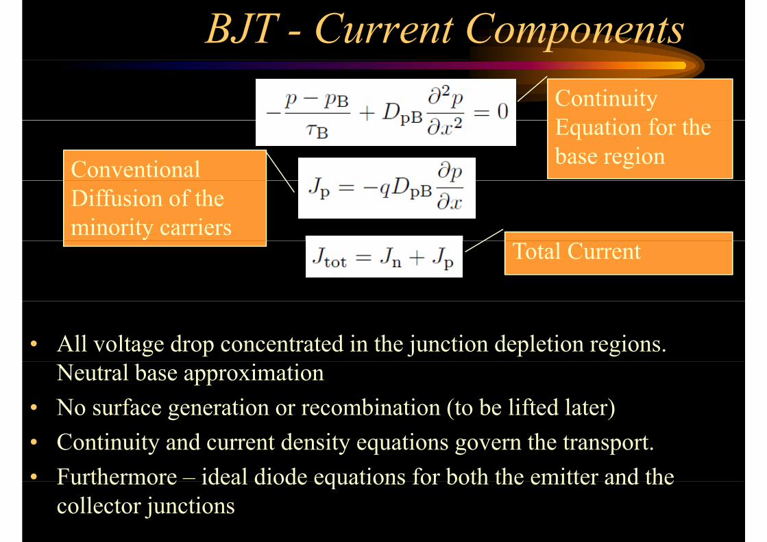
BJT - Current ComponentsContinuityE ti f thEquation for thebase regionConventional
Diffusion of theminority carriers
Total Current
• All voltage drop concentrated in the junction depletion regions. Neutral base approximation
• No surface generation or recombination (to be lifted later)• Continuity and current density equations govern the transport.• Furthermore – ideal diode equations for both the emitter and theFurthermore ideal diode equations for both the emitter and the
collector junctions

BJT – Schematic 1D DiagramNd
+-Na-
wE wB wC
-xE -xC
x

Excess Carrier Balance
At the emitterAt the emitterdepletion-layeredgesedges.
At the collectordepletion layerdepletion-layeredges.
• p n and n are the equilibrium carrier concentrations in the base• pB, nE and nC are the equilibrium carrier concentrations in the base, emitter and collector, respectively.Id l di d ti• Ideal diode equations.
• The most important contribution is, the minority holes in the base.
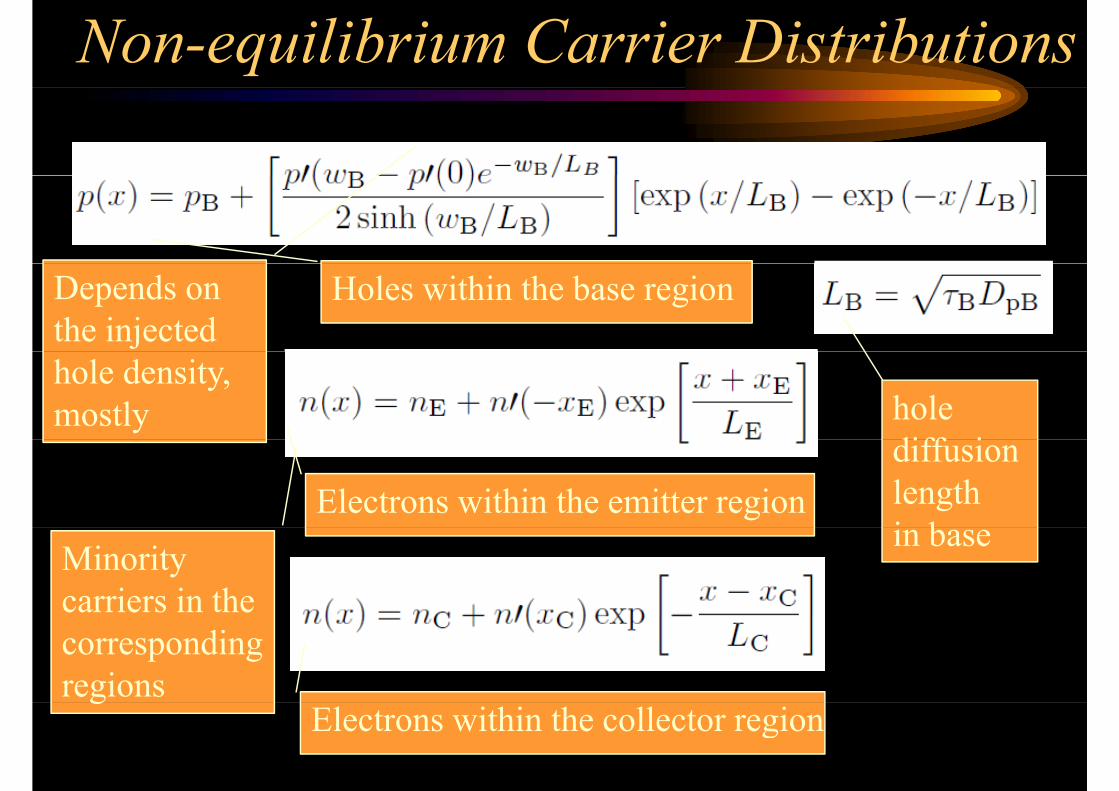
Non-equilibrium Carrier Distributions
Holes within the base regionDepends onthe injected
holediff i
hole density,mostly
Electrons within the emitter regiondiffusionlengthi bin base
Minoritycarriers in thecorrespondingregions
Electrons within the collector regiong
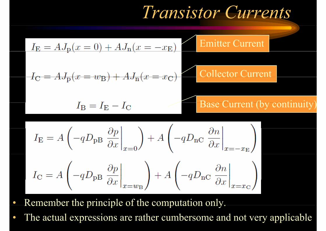
Transistor CurrentsEmitter Current
Collector CurrentCo ecto Cu e t
Base C rrent (b contin it )Base Current (by continuity)
• Remember the principle of the computation only.Remember the principle of the computation only.• The actual expressions are rather cumbersome and not very applicable
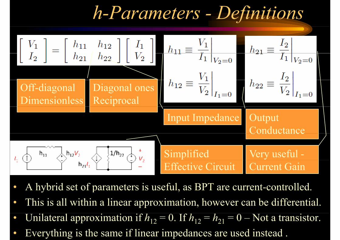
h-Parameters - Definitions
Off-diagonalDimensionless
Diagonal onesReciprocal
Input Impedance Output ConductanceConductance
Very useful -Simplified
• A hybrid set of parameters is useful as BPT are current controlled
Current GainEffective Circuit
• A hybrid set of parameters is useful, as BPT are current-controlled.• This is all within a linear approximation, however can be differential.• Unilateral approximation if h12 = 0. If h12 = h21 = 0 – Not a transistor.• Everything is the same if linear impedances are used instead .
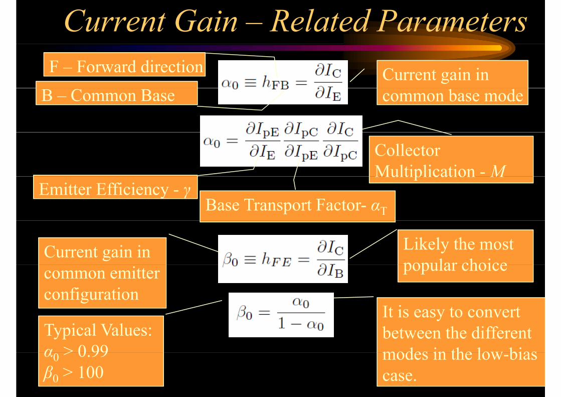
Current Gain – Related ParametersCurrent gain inF – Forward directioncommon base modeB – Common Base
CollectorMultiplication - M
Emitter Efficiency - γBase Transport Factor- αT
Multiplication M
Likely the most popular choice
Current gain in popular choice
It i t t
common emitterconfiguration
It is easy to convertbetween the differentmodes in the low bias
Typical Values:α > 0 99 modes in the low-bias
case.α0 > 0.99β0 > 100

How to Estimate the Current Gain?
Common base current gainEmitter efficiency
Base transport factor
Collector Multiplicationp
The Famous hFE

Rough Estimate of the Current Gain...Effective base widthhas to be thin to achievehigh gainsBase diffusion length –
the longer – the betterthe longer the betterCollector Multiplication Can be higher in
real transistors andreal transistors andat high collector bias–
Emitter efficiencyThe base transportfactor would typicallyEmitter efficiency
would normally bethe dominant factor
yp ybe very close to unity
The common basecurrent gain
Typical of popularTypical of popularbipolar transistors

Output CharacteristicsA typical set of characteristics is shown (right) for the output current Icvs output voltage V for different base currents I for the case of thevs output voltage Vce for different base currents Ib for the case of the BPT ‘common emitter’ circuit configuration (left – p-n-p shown).
Note the almost lineardependence of the Saturation current on Ib

The Early Effect - (J. M. Early 1952) Points
(i)
–
(iii)
(ii) I ≠ 0 for Ib = 0 because of leakage effects at the collector(i) Common emitter current gain of this transistor ≈ 400 (from fig. !)(ii) Ic ≠ 0 for Ib = 0 because of leakage effects at the collector-base junction (neglected in this analysis). (iii) Th h t i ti l d i th i i ith(iii) The characteristics slope upwards, i.e. the gain increases with increasing Vce.This is because the reverse voltage Vcb across the collector-base junction = Vce–Vbe ≈ Vce– 0.6 V and is
h f l i itherefore also increasing.
The collector-base depletion player width is increasing.
The effective base width, wn, is decreasing to wn’ (see figure).is decreasing to wn (see figure).

Bipolar Transistors - Usage
Basic DC biasing concept
Basic AC decoupling
• Common emitter is the most abundant circuit connection type.• Typically Resistor dividers are used for DC biasing• Typically Resistor dividers are used for DC biasing.• Decoupling capacitors are used extensively for AC decoupling.• There is no direct way to provide for bipolar amplification (later• There is no direct way to provide for bipolar amplification (later other examples will be provided within unipolar devices)