drv10983, drv10975, drv10983-q1, and drv10987 …
TRANSCRIPT

LM3478
TPD3S014
USB/Other ON/OFF
12-V to 26-V VIN
5-V USB VIN
ON/OFF Logic
TPS63070
2-V to16-V VIN
DRV10983DRV10975
DRV10983-Q1DRV10987
Socket
DRV10983DRV10975
DRV10983-Q1DRV10987
Socket
DRV10983DRV10975
DRV10983-Q1DRV10987
Socket
DRV10983DRV10975
DRV10983-Q1DRV10987
Socket
DRV10983DRV10975
DRV10983-Q1DRV10987
Socket
DRV10983DRV10975
DRV10983-Q1DRV10987
Socket
DRV10983DRV10975
DRV10983-Q1DRV10987
Socket
DRV10983DRV10975
DRV10983-Q1DRV10987
Socket
Socket Board
Programming Board
ON/OFF Signal (across boards)
MSP430G2553
LCD Screen
GPIO Buttons (5X)
SN74LV4T125
SN74LV4T125
SN74LV4T12511 11
5TPD8E003ESD
ProtectionISO1541DRI2C
SDASCL
5 V
5 V
5-V iso
4
3v3
3v3
5-V iso
DCP010505B
3v3 iso
LP5907 3.3
TCA9548A
I2CSDASCLiso
I2C - SDA SCL iso(across boards)
16
LP5907 3.3
TPD8E003ESD
Protection
TPD8E003ESD
Protection
Copyright © 2017, Texas Instruments Incorporated
1TIDUCX2A–March 2017–Revised October 2017Submit Documentation Feedback
Copyright © 2017, Texas Instruments Incorporated
DRV10983, DRV10975, DRV10983-Q1, and DRV10987 EEPROMProgramming Tool Reference Design
TI Designs: TIDA-01373DRV10983, DRV10975, DRV10983-Q1, and DRV10987EEPROM Programming Tool Reference Design
DescriptionThe TIDA-01373 is a reference hardware and softwareexample of a scalable programming tool for theDRV10983, DRV10975, DRV10983 -Q1, andDRV10987 integrated BLDC motor drivers. Thesedevices feature configurable EEPROM registers thatmust be set to motor-specific parameters. Thisreference design provides details on how to programup to eight EEPROM registers of a motor driver devicewith user-specified motor parameter values.
Resources
Design FolderTIDA-01373Product FoldersDRV10983 DRV10975 DRV10983-Q1 DRV10987MSP430G2553 TCA9548A TPS630701 TPD3S014LP5907-3.3 SN74LV4T125 DCP010505B ISO1541DRLM3478 TPD8E003
ASK Our E2E Experts
Features• Software and Hardware Support up to Eight
Devices• User-Configurable EEPROM Settings• Single ON and OFF Switch• Overvoltage Protection• Power Supply Isolation• Two-Wire JTAG Interface to MCU• DRV10983, DRV10975, DRV10983-Q1, and
DRV10987 EEPROM Software Examples• LCD Screen for User to Read Back Verification• ESD Protection for GPIO and I2C Interfaces
Applications• EEPROM Programming Tool

System Description www.ti.com
2 TIDUCX2A–March 2017–Revised October 2017Submit Documentation Feedback
Copyright © 2017, Texas Instruments Incorporated
DRV10983, DRV10975, DRV10983-Q1, and DRV10987 EEPROMProgramming Tool Reference Design
An IMPORTANT NOTICE at the end of this TI reference design addresses authorized use, intellectual property matters and otherimportant disclaimers and information.
1 System DescriptionThe DRV10983, DRV10975, DRV10983-Q1, and DRV10987 are integrated brushless DC (BLDC) motordrivers with configurable, electrically erasable programmable read-only memory (EEPROM) registers thatmust be set to motor-specific parameters. The EEPROM registers can be written to and read from throughI2C protocol.
The TIDA-01373 is a hardware and software reference design for a DRV10983, DRV10975, DRV10983-Q1, and DRV10987 programming tool. The design is intended to be used as an example of how ascalable programming tool may be built to program the configurable registers of the DRV10983,DRV10975, DRV10983-Q1, and DRV10987 devices through the I2C protocol described in the I2C SerialInterface sections of the respective device data sheet [1] [2] [3].
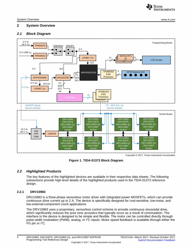
The TIDA-01373 hardware consists of two separate printed-circuit boards (PCBs). The first board isreferred to as the programming board and the second board is referred to as the socket board. Theprogramming board consists of power management, whole system ON and OFF switch, microcontroller(MCU), I2C multiplexer (MUX), liquid-crystal display (LCD), buttons, and isolation. The socket boardconsists of power management and eight sockets in which the DRV10983, DRV10975, DRV10983-Q1, orDRV10987 motor driver is placed. The two boards are connected through two ribbon wires: one for the I2Ccommunication lines as well as an ON and OFF signal and one for a ground connection. Overvoltageprotection is built into both boards as well as isolation to protect both the motor drivers and the MCU in thesystem.
The design allows for a user to select custom motor parameter settings to program the DRV10983,DRV10975, DRV10983-Q1, and DRV10987 EEPROM registers by editing a header file found in thesource code. The user manually inputs the parameters with the desired values that are generated whenthe motor has been tuned. The source code is then compiled and flashed to the MSP430G2553 MCU onthe programming board. The design offers a two-wire JTAG interface to the MCU to reduce the pin count.When the MCU is flashed the TIDA-01373 is a stand-alone system. The LCD on the programming boardallows for user-friendly operation of the design.
The TIDA-01373 has three general functions during operation. The first function reads back to the user thevalues that are to be programmed into the EEPROM registers of the DRV10983, DRV10975, DRV10983-Q1, and DRV10987 devices for the motor parameters. These values correspond to the values entered bythe user into the header file in the source code. The second function reads the DRV10983, DRV10975,DRV10983-Q1, or DRV10987 devices that are in the system and verifies that the EEPROM registers ineach of the devices match the desired values in the header file. This function indicates which deviceshave EEPROM registers that match and which ones do not. The third function is the general programmingroutine. This function writes the desired motor parameter values that the user has specified in the headerfile to the EEPROM registers in each of the populated DRV10983, DRV10975, DRV10983-Q1, orDRV10987 motor drivers on the socket board. This function then verifies that all of the devices have beenproperly programmed and indicates back to the user if any errors occur.
www.ti.com System Description
3TIDUCX2A–March 2017–Revised October 2017Submit Documentation Feedback
Copyright © 2017, Texas Instruments Incorporated
DRV10983, DRV10975, DRV10983-Q1, and DRV10987 EEPROMProgramming Tool Reference Design
1.1 System Benefits• Scalability
– Hardware example can be used to scale up to more than eight motor drivers– Software examples can be used to scale up to more than eight motor drivers
• Software examples– Example I2C routines to communicate with the DRV10983, DRV10975, DRV10983-Q1, and
DRV10987 devices– Example routines for users to learn how to read from the DRV10983, DRV10975, DRV10983-Q1,
and DRV10987– Example routines for users to learn how to write to the configuration registers on the DRV10983,
DRV10975, DRV10983-Q1, and DRV10987– Validation feedback given immediately after programming is completed
• Highly integrated– Stand-alone system requires no computer in General Operation Mode– Solution allows user to simultaneously program up to eight devices increasing programming times– JTAG interface allows quick MCU-flashing capabilities for a complete software and hardware
solution• Fully protected
– Overvoltage protection integrated into both boards through transient voltage suppression (TVS)diodes
– I2C software protection for unpopulated sockets; allows user to verify proper population of devices– ESD protection for both general port input/output (GPIO) buttons and I2C communication– Single ON and OFF switch for easy operation with minimal interference
1.2 Key System Specifications
Table 1. Key System Specifications—Programming Board
PARAMETER DESCRIPTION SPECIFICATIONVIN VIN from DC power supply 2 V to 16 VUSB_VIN USB input voltage 4.8 V to 5.2 VTest Test pin used in two-wire JTAG 3.3 VReset Reset pin used in two-wire JTAG 3.3 V
Table 2. Key System Specifications—Socket Board
PARAMETER DESCRIPTION SPECIFICATIONVIN VIN from DC power supply 12 V to 26 V
Cable length I2C ribbon cable length 6 in
LM3478
TPD3S014
USB/Other ON/OFF
12-V to 26-V VIN
5-V USB VIN
ON/OFF Logic
TPS63070
2-V to16-V VIN
DRV10983DRV10975
DRV10983-Q1DRV10987
Socket
DRV10983DRV10975
DRV10983-Q1DRV10987
Socket
DRV10983DRV10975
DRV10983-Q1DRV10987
Socket
DRV10983DRV10975
DRV10983-Q1DRV10987
Socket
DRV10983DRV10975
DRV10983-Q1DRV10987
Socket
DRV10983DRV10975
DRV10983-Q1DRV10987
Socket
DRV10983DRV10975
DRV10983-Q1DRV10987
Socket
DRV10983DRV10975
DRV10983-Q1DRV10987
Socket
Socket Board
Programming Board
ON/OFF Signal (across boards)
MSP430G2553
LCD Screen
GPIO Buttons (5X)
SN74LV4T125
SN74LV4T125
SN74LV4T12511 11
5TPD8E003ESD
ProtectionISO1541DRI2C
SDASCL
5 V
5 V
5-V iso
4
3v3
3v3
5-V iso
DCP010505B
3v3 iso
LP5907 3.3
TCA9548A
I2CSDASCLiso
I2C - SDA SCL iso(across boards)
16
LP5907 3.3
TPD8E003ESD
Protection
TPD8E003ESD
Protection
Copyright © 2017, Texas Instruments Incorporated
System Overview www.ti.com
4 TIDUCX2A–March 2017–Revised October 2017Submit Documentation Feedback
Copyright © 2017, Texas Instruments Incorporated
DRV10983, DRV10975, DRV10983-Q1, and DRV10987 EEPROMProgramming Tool Reference Design
2 System Overview
2.1 Block Diagram
Figure 1. TIDA-01373 Block Diagram
2.2 Highlighted ProductsThe key features of the highlighted devices are available in their respective data sheets. The followingsubsections provide high-level details of the highlighted products used in the TIDA-01373 referencedesign.
2.2.1 DRV10983DRV10983 is a three-phase sensorless motor driver with integrated power MOSFETs, which can providecontinuous drive current up to 2 A. The device is specifically designed for cost-sensitive, low-noise, andlow-external-component count applications.
The DRV10983 uses a proprietary, sensorless control scheme to provide continuous sinusoidal drive,which significantly reduces the pure tone acoustics that typically occur as a result of commutation. Theinterface to the device is designed to be simple and flexible. The motor can be controlled directly throughpulse-width modulation (PWM), analog, or I2C inputs. Motor speed feedback is available through either theFG pin or I2C.
www.ti.com System Overview
5TIDUCX2A–March 2017–Revised October 2017Submit Documentation Feedback
Copyright © 2017, Texas Instruments Incorporated
DRV10983, DRV10975, DRV10983-Q1, and DRV10987 EEPROMProgramming Tool Reference Design
The DRV10983 features an integrated buck and linear regulator to efficiently step down the supply voltageto either 5 V or 3.3 V for powering both internal and external circuits. The device is available in either asleep mode or standby mode version to conserve power when the motor is not running. The standbymode version (3 mA) leaves the regulator running and the sleep mode version (180 µA) shuts it off. Usethe standby mode version in applications where the regulator is used to power an external MCU [1].
An I2C interface allows the user to reprogram specific motor parameters in registers and program theEEPROM to help optimize the performance for a given application. The DRV10983 is available in athermally-efficient HTSSOP, 24-pin package with an exposed thermal pad. The operating temperature isspecified from –40°C to 125°C.
2.2.2 DRV10975The DRV10975 is a three-phase sensorless motor driver with integrated power MOSFETs, which canprovide continuous drive current up to 1.5 A. The device is specifically designed for cost-sensitive, low-noise and low-external-component count applications.
The DRV10975 uses a proprietary, sensorless control scheme to provide continuous sinusoidal drive,which significantly reduces the pure tone acoustics that typically occur as a result of commutation. Theinterface to the device is designed to be simple and flexible. The motor can be controlled directly throughPWM, analog, or I2C inputs. Motor speed feedback is available through either the FG pin or I2C.
The DRV10975 features an integrated buck and linear regulator to efficiently step down the supply voltageto either 5 V or 3.3 V for powering both internal and external circuits. The device is available in either asleep mode or a standby mode version to conserve power when the motor is not running. The standbymode version (4.5 mA) leaves the regulator running and the sleep mode version (80 µA) shuts it off. Usethe standby mode version in applications where the regulator is used to power an external MCU.
An I2C interface allows the user to reprogram specific motor parameters in registers and program theEEPROM to help optimize the performance for a given application. The DRV10975 is available in athermally-efficient HTSSOP, 24-pin package with an exposed thermal pad. The operating temperature isspecified from –40°C to 125°C [2].
2.2.3 DRV10983-Q1The DRV10983-Q1 device is a three-phase sensorless motor driver with integrated power MOSFETs,which can provide continuous drive current up to 2 A. The device is specifically designed for cost-sensitive, low noise, low-external-component-count fan and pump applications.
The DRV10983-Q1 device protects the nonvolatile memory down to 4.5 V and delivers current to themotor with a supply voltage as low as 6.2 V. If the power supply voltage is higher than 28 V, the devicestops driving the motor and protects the DRV10983- Q1 circuitry. This function is able to handle a loaddump condition up to 45 V [3].
2.2.4 DRV10987
The DRV10987 device is a three-phase, sensorless, 180° sinusoidal motor driver with integrated powerMOSFETs which can provide continuous drive current up to 2 A. The device is specifically designed forcost-sensitive, low-noise, low-external-component-count fan and pump applications.
The DRV10987 device delivers current to the motor with a supply voltage as low as 6.2 V. If the powersupply voltage is higher than 28 V, the device stops driving the motor and protects the DRV10987circuitry.
2.2.5 MSP430G2553The Texas Instruments MSP430™ family of ultra-low-power microcontrollers consists of several devicesfeaturing different sets of peripherals targeted for various applications. The architecture, combined withfive low-power modes, is optimized to achieve extended battery life in portable measurement applications.The device features a powerful 16-bit RISC CPU, 16-bit registers, and constant generators that contributeto maximum code efficiency.

System Overview www.ti.com
6 TIDUCX2A–March 2017–Revised October 2017Submit Documentation Feedback
Copyright © 2017, Texas Instruments Incorporated
DRV10983, DRV10975, DRV10983-Q1, and DRV10987 EEPROMProgramming Tool Reference Design
The digitally controlled oscillator (DCO) allows wakeup from low-power modes to active mode in less than1 μs. The MSP430G2x13 and MSP430G2x53 series are ultra-low-power, mixed-signal MCUs with built-in16-bit timers, up to 24 I/O capacitive-touch enabled pins, a versatile analog comparator, and built-incommunication capability using the universal serial communication interface. In addition, theMSP430G2x53 family members have a 10-bit analog-to-digital converter (ADC). Typical applicationsinclude low-cost sensor systems that capture analog signals, convert them to digital values, and thenprocess the data for display or for transmission to a host system [5].
2.2.6 TCA9548AThe TCA9548A device has eight bidirectional translating switches that can be controlled through the I2Cbus. The SCL/SDA upstream pair fans out to eight downstream pairs, or channels. Any individualSCn/SDn channel or combination of channels can be selected, which is determined by the contents of theprogrammable control register. These downstream channels can be used to resolve I2C slave addressconflicts. For example, if eight identical digital temperature sensors are required in the application, onesensor can be connected at each channel: 0-7. The system master can reset the TCA9548A device in theevent of a time-out or other improper operation by asserting a low in the RESET input. Similarly, thepower-on reset deselects all channels and initializes the I2C (SMBus) state machine. Asserting RESETcauses the same reset and initialization to occur without powering down the part. This feature allowsrecovery if one of the downstream I2C buses get stuck in a low state. The pass gates of the switches areconstructed so that the VCC pin can be used to limit the maximum high voltage, which is passed by theTCA9548A device. Limiting the maximum high voltage allows the use of different bus voltages on eachpair, so that 1.8-V, 2.5- V or 3.3-V parts can communicate with 5-V parts without any additional protection.External pullup resistors pull the bus up to the desired voltage level for each channel. All I/O pins are 5-Vtolerant [6].
2.2.7 TPS63070The TPS6307x is a high-efficiency, low-quiescent current, buck-boost converter suitable for applicationswhere the input voltage can be higher or lower than the output voltage. Output currents can go as high as2 A in boost mode and in buck mode. The buck-boost converter is based on a fixed-frequency PWMcontroller using synchronous rectification to obtain maximum efficiency. At low load currents, the converterenters power save mode to maintain high efficiency over a wide-load current range. The converter can bedisabled to minimize battery drain. During shutdown, the load is disconnected from the battery. The deviceis available in a 2.5×3-mm QFN package [7].
2.2.8 TPD3S014The TPD3S0x4 series of integrated devices feature a current-limited load switch and a two-channel, TVS-based, electrostatic discharge (ESD) protection diode array for USB interfaces.
The TPD3S0x4 devices are intended for applications such as USB where heavy capacitive loads andshort circuits are likely to be encountered; TPD3S0x4 devices provide short-circuit protection andovercurrent protection. The TPD3S0x4 limits the output current to a safe level by operating in constantcurrent mode when the output load exceeds the current limit threshold. The fast overload response easesthe burden on the main 5-V power supply by quickly regulating the power when the output is shorted. Therise and fall times for the current limit switch are controlled to minimize current surges when turning thedevice on and off.
The TPD3S014 and TPD3S044 allow 0.5 A and 1.5 A of continuous current, respectively. The TVS diodearray is rated to dissipate ESD strikes above the maximum level specified in the IEC 61000-4-2international standard.
The high level of integration, combined with its easy-to-route DBV package, allows this device to providegreat circuit protection for USB interfaces in applications like laptops, high-definition digital TVs, set-topboxes, and electronic point-of-sale equipment [8].
www.ti.com System Overview
7TIDUCX2A–March 2017–Revised October 2017Submit Documentation Feedback
Copyright © 2017, Texas Instruments Incorporated
DRV10983, DRV10975, DRV10983-Q1, and DRV10987 EEPROMProgramming Tool Reference Design
2.2.9 LP5907-3.3The LP5907 is a low-noise linear-dropout regulator (LDO) that can supply up to 250 mA of output current.Designed to meet the requirements of RF and analog circuits, the LP5907 device provides low noise, highpower supply rejection ratio (PSRR), low quiescent current, and low line or load transient responsefigures. Using new innovative design techniques, the LP5907 offers class-leading noise performancewithout a noise bypass capacitor and the ability for remote output capacitor placement. The device isdesigned to work with a 1-μF input and a 1-μF output ceramic capacitor and does not require a separatenoise bypass capacitor. This device is available with fixed output voltages from 1.2 V to 4.5 V in 25-mVsteps [9].
2.2.10 SN74LV4T125SN74LV4T125 is a low-voltage complementary metal-oxide-semiconductor (CMOS) buffer gate whichoperates at a wider voltage range for portable, telecom, industrial, and automotive applications. The outputlevel is referenced to the supply voltage and is able to support 1.8-V, 2.5-V, 3.3-V, and 5-V CMOS levels.
The input is designed with a lower threshold circuit to match 1.8-V input logic at VCC = 3.3 V and can beused in 1.8-V to 3.3-V level-up translation. In addition, the 5-V tolerant input pins enable down translation(for example, 3.3-V to 2.5-V output at VCC = 2.5 V). The wide VCC range of 1.8 V to 5.5 V allows thegeneration of desired output levels to connect to controllers or processors.
The SN74LV4T125 device is designed with current-drive capability of 8 mA to reduce line reflections,overshoot, and undershoot caused by high-drive outputs [10].
2.2.11 DCP010505BThe DCP01B series is a family of 1-W, isolated, unregulated DC-DC converter modules. Requiring aminimum of external components and including on-chip device protection, the DCP01B series of devicesprovide extra features such as output disable and synchronization of switching frequencies.
This combination of features and small size makes the DCP01B series of devices suitable for a widerange of applications and is an easy-to-use solution in applications requiring signal path isolation [11].
2.2.12 ISO1541DRThe ISO1540 and ISO1541 devices are low-power, bidirectional isolators that are compatible with I2Cinterfaces. These devices have logic input and output buffers that are separated by Texas Instrument'scapacitive isolation technology using a silicon dioxide (SiO2) barrier. When used with isolated powersupplies, these devices block high voltages, isolate grounds, and prevent noise currents from entering thelocal ground and interfering with or damaging sensitive circuitry.
This isolation technology provides for function, performance, size, and power consumption advantageswhen compared to optocouplers. The ISO1540 and ISO1541 devices enable a complete isolated I2Cinterface to be implemented within a small form factor.
The ISO1540 has two isolated bidirectional channels for clock and data lines while the ISO1541 has abidirectional data and a unidirectional clock channel. The ISO1541 is useful in applications that have asingle master while the ISO1540 is suitable for multi-master applications. For applications where clockstretching by the slave is possible, the ISO1540 device should be used.
Isolated bidirectional communication is accomplished within these devices by offsetting the low-leveloutput voltage on side 1 to a value greater than the high-level input voltage on side 1, thus preventing aninternal logic latch that otherwise would occur with standard digital isolators [12].
System Overview www.ti.com
8 TIDUCX2A–March 2017–Revised October 2017Submit Documentation Feedback
Copyright © 2017, Texas Instruments Incorporated
DRV10983, DRV10975, DRV10983-Q1, and DRV10987 EEPROMProgramming Tool Reference Design
2.2.13 LM3478The LM3478 is a versatile low-side, N-Channel MOSFET controller for switching regulators. The controlleris suitable for use in topologies requiring a low-side MOSFET, such as boost, flyback, single-endedprimary-inductor converter (SEPIC), and so forth. Moreover, the LM3478 can be operated at an extremely-high switching frequency to reduce the overall solution size. The switching frequency of the LM3478 canbe adjusted to any value between 100 kHz and 1 MHz by using a single external resistor. Current modecontrol provides superior bandwidth and transient response, besides cycle-by-cycle current limiting. Outputcurrent can be programmed with a single external resistor.
The LM3478 has built-in features such as thermal shutdown, short-circuit protection, overvoltageprotection, and so forth. Power-saving shutdown mode reduces the total supply current to 5 µA and allowspower supply sequencing. An internal soft-start limits the inrush current at start-up [13].
2.2.14 TPD8E003The TPD8E003 device is a unidirectional, TVS-based, ESD protection diode array. The TPD8E003 israted to dissipate ESD strikes above the maximum level specified in the IEC 61000-4-2 internationalstandard (level 4). This device provides eight channels of ESD protection in a space-saving WSONpackage. Typical applications for the TPD8E003 include keypad, GPIO, resistive touchscreen, and low-speed memory interfaces. See the TPD2E2U06 and TPD4E05U06 for two- and four-channel ESDprotection solutions, respectively [14].
GND1
Vin
5v-Other-Reg
22µFC1
10.0k
R1
0.1µFC2
100kR35
10µFC3
47µFC4
1.5µH
L1
F10263001.WRT1L
F3
0263001.WRT1L
PS/SYNC1
PG2
VAUX3
GND4
FB5
FB26
VOUT7
L29
PGND10
L111
VIN13
EN14
VSEL15
VOUT8
VIN12
U1
TPS630701RNMR
Copyright © 2017, Texas Instruments Incorporated
www.ti.com Hardware, Software, and Test Results
9TIDUCX2A–March 2017–Revised October 2017Submit Documentation Feedback
Copyright © 2017, Texas Instruments Incorporated
DRV10983, DRV10975, DRV10983-Q1, and DRV10987 EEPROMProgramming Tool Reference Design
3 Hardware, Software, and Test Results
3.1 Required Hardware and SoftwareThis section outlines the required hardware and software that make up the TIDA-01373 reference design
3.1.1 HardwareTo get started with using the hardware, see the TIDA-01373 Quick Start User's Guide [4].
3.1.1.1 Programming BoardThe programming board consists of a power management and a system ON and OFF switch, MCU, I2Cmultiplexer (MUX), LCD, buttons, and isolation.
3.1.1.1.1 Power StageThe power stage of the programming board provides many different options for the user to power theboard:• 6-V to 12-V wall socket (barrel power connector)• External power supply with clips (test-point connection)• External power supply using wires (screw terminal block)• USB power interface (micro-USB port)
Because of the additional USB power interface, two different regulators have been built into the system:one for the USB power interface and one for all other possible power supply options. The user must selectwhich option with which to power the system through a control switch.
In addition to these regulators, the design also features a built-in 3V3 LDO that bucks the 5-V regulatedrail from the power supply down to 3.3 V to supply the onboard MCU.
The following subsections outline the design considerations for the three different regulators as well as thecontrol switches.
3.1.1.1.1.1 TPS630Figure 2 shows the configuration of the TPS630701 5-V regulator in the TIDA-01373 system. Thisregulator is responsible for regulating an external DC power supply other than a USB input.
Figure 2. TPS630701 Configuration
( )OUT IN
PEAKƒ
I V
L
DI
1 D 2
´= +
h ´ - ´´
OUT IN
OUT
V VDuty Cycle Boost: D
V
-
=
Hardware, Software, and Test Results www.ti.com
10 TIDUCX2A–March 2017–Revised October 2017Submit Documentation Feedback
Copyright © 2017, Texas Instruments Incorporated
DRV10983, DRV10975, DRV10983-Q1, and DRV10987 EEPROMProgramming Tool Reference Design
The TPS6307x series of buck-boost converter features internal loop compensation; therefore, the externalL-C filter has to be selected according to the internal compensation. One important factor to consider isthat the effective inductance, due to inductor tolerance and current derating, can vary between 20% and–30%. The same consideration applies for the capacitance of the output filter: The effective capacitancecan vary between 20% and –80% of the specified data sheet value, due to capacitor tolerance and biasvoltage.
Programming the output voltageWhile the output voltage of the TPS63070 is adjustable, the TPS630701 is set to a fixed voltage. Forfixed-output versions, the FB pin must be connected to the output directly.
Inductor selectionFor high efficiencies, the inductor must have a low DC resistance to minimize conduction losses. The corematerial has a higher impact on efficiency, especially at high switching frequencies. When using small-chipinductors, the efficiency is reduced mainly due to higher inductor core losses, which must be taken intoconsideration when selecting the appropriate inductor. The inductor value determines the inductor ripplecurrent. The larger the inductor value, the smaller the inductor ripple current and the lower the conductionlosses of the converter. Conversely, larger inductor values cause a slower load transient response. Toavoid saturation of the inductor, the peak current for the inductor in steady-state operation is calculatedusing Equation 1. Only the equation which defines the switch current in boost mode is shown, becausethis provides the highest value of current and represents the critical current value for selecting the rightinductor.
(1)
Where:• D = Duty cycle in boost mode,• ƒ = Converter switching frequency (typical 2.4 MHz),• L = Selected inductor value,• η = Estimated converter efficiency (use the number from the efficiency curves or 0.90 as an
assumption).
NOTE: The calculation must be done for the minimum input voltage, which is possible to have inboost mode.
Input capacitorTI recommends to use a combination of capacitors on the input: a small-size ceramic capacitor as closeas possible from the VIN pin to GND1 to block high-frequency noise and a larger one in parallel for therequired capacitance for good transient behavior of the regulator. The use of X5R or X7R ceramiccapacitors are recommended. The input capacitor must be large enough to avoid supply voltage dipsshorter than 5 µs because the undervoltage lockout (UVLO) circuitry requires time to react.
Output capacitorSame as the input, the output capacitor should be a combination of capacitors optimized for suppressinghigh-frequency noise and a larger capacitor for low-output voltage ripple and stable operation. The use ofsmall X5R or X7R ceramic capacitors placed as close as possible to the VOUT and GND pins of the IC isrecommended. The best configuration is a 0603-size capacitor close to the pins of the IC and as many0805 capacitors as required to get the capacitance considering the output voltage and DC bias effect ofthe ceramic capacitors. Larger capacitors cause a lower-output voltage ripple as well as a lower-outputvoltage drop during load transients [7].
1000 ohm
L2
5v-USB-Reg
F20263001.WRT1L
5v_pre
5v_pre
USB_Vin
GND1
0.1µFC25
4.7µFC24
EN1
GND2
IN3
OUT4
D15
D26
U10
TPD3S014DBVRGND1
Copyright © 2017, Texas Instruments Incorporated
www.ti.com Hardware, Software, and Test Results
11TIDUCX2A–March 2017–Revised October 2017Submit Documentation Feedback
Copyright © 2017, Texas Instruments Incorporated
DRV10983, DRV10975, DRV10983-Q1, and DRV10987 EEPROMProgramming Tool Reference Design
3.1.1.1.1.2 TPD3S014Figure 3 shows the configuration of the TPD3S014 device in the TIDA-01373 system. The TPD3S014 is aregulator for a USB power supply input.
Figure 3. TPD3S014 Configuration
TPD3S014 capacitor selectionInput and output capacitance improves the performance of the device; the actual capacitance should beoptimized for the particular application. For all applications, a 0.1 μF or greater ceramic bypass capacitorbetween USB_IN and GND1 is recommended as close to the device as possible for local noisedecoupling.
All protection circuits such as the TPD3S0x4s have the potential for input voltage overshoots and outputvoltage undershoots.
Input voltage overshoots can be caused by either of two effects. The first cause is an abrupt application ofinput voltage in conjunction with input power bus inductance and input capacitance when the IN terminal ishigh impedance (before turnon). Theoretically, the peak voltage is two times the applied voltage. Thesecond cause is due to the abrupt reduction of output short-circuit current when the TPD3S0x4s turn offand energy stored in the input inductance drives the input voltage high. Input voltage droops may alsooccur with large load steps and as the TPD3S0x4s outputs are shorted. Applications with large inputinductance (for example, connecting the evaluation board to the bench power supply through long cables)may require large input capacitance to reduce the voltage overshoot from exceeding the absolutemaximum voltage of the device. The fast current-limit speed of the TPD3S0x4s to hard output shortcircuits isolates the input bus from faults. However, ceramic input capacitance in the range of 1 µF to22 μF adjacent to the TPD3S0x4s inputs aids in both speeding the response time and limiting the transientseen on the input power bus. Momentary input transients to 6.5 V are permitted.
Output voltage undershoot is caused by the inductance of the output power bus just after a short hasoccurred and the TPD3S0x4s have abruptly reduced OUT current. Energy stored in the inductance drivesthe OUT voltage down and potentially to a negative value as it discharges. Applications with large outputinductance (such as from a cable) benefit from use of a high-value output capacitor to control the voltageundershoot. When implementing USB standard applications, a 120-μF minimum output capacitance isrequired. Typically a 150-μF electrolytic capacitor is used, which is sufficient to control voltageundershoots. However, if the application does not require 120 μF of capacitance, and there is potential todrive the output negative, a minimum of 10-μF ceramic capacitance on the output is recommended. Thevoltage undershoot should be controlled to less than 1.5 V for 10 μs [8].

( )D IN OUT OUTP V V I= - ´
Power for MCU and I C2
GND1
VIN1
GND2
EN3
N/C4
VOUT5
U2
LP5907MFX-3.3/NOPB
0.1µFC17
4.7µFC18
3v35v
Copyright © 2017, Texas Instruments Incorporated
12
GreenPWRLED
QTLP630C4TR
GND1
270R33
5v1
3
2
S2_usb/other
5v_pre
5v-Other-Reg
5v-USB-Reg 5v
5v_pre
GND1
2
1
3
S1on/off
Copyright © 2017, Texas Instruments Incorporated
Hardware, Software, and Test Results www.ti.com
12 TIDUCX2A–March 2017–Revised October 2017Submit Documentation Feedback
Copyright © 2017, Texas Instruments Incorporated
DRV10983, DRV10975, DRV10983-Q1, and DRV10987 EEPROMProgramming Tool Reference Design
3.1.1.1.1.3 Control SwitchesFigure 4 shows the control switches for the system
Figure 4. TIDA-01373 System Control Switches—Programming Board
The control switches for the system consist of two switches: a USB or other switch and an ON and OFFswitch. When initially setting up the design, the user must first select how they are going to power theprogramming board. If the user plans to use a USB power supply, they must flip the USB or other switchto the “USB” state, and if they are using another DC power supply, the user must flip the switch to the“Other” state.
The ON and OFF switch is used when the system is in general use. This switch can be flipped on and offper the instruction in the TIDA-01373 Quick Start User’s Guide [4]. The ON and OFF switch also sends a5-V signal from the programming board to the socket board when turned on and a 0-V signal when turnedoff. Logic on the socket board allows this one switch to control the whole system.
3.1.1.1.1.4 LP5907 3v3 LDOFigure 5 details the LDO in the system that provides power to the MCU and voltage levels for the logic aswell as I2C communication lines.
Figure 5. LP5907 Configuration for 3V3 Rail
Output capacitance selection and placementThe LP5907 device requires at least a 1-μF capacitor at the OUT pin, but there are no strict requirementsabout the location of the capacitor in regards the OUT pin. In practical designs, the output capacitor maybe located up to 10-cm away from the LDO.
Device power dissipationThe actual power being dissipated in the device can be represented by Equation 2 [9]:
(2)
A01
A12
RESET3
SD04
SC05
SD16
SC17
SD28
SC29
SD310
SC311
GND12
SD413
SC414
SD515
SC516
SD617
SC618
SD719
SC720
A221
SCL22
SDA23
VCC24
U9
TCA9548APW
4.70k
R12
4.70k
R13
4.70k
R14
4.70k
R15
4.70k
R16
4.70k
R17
4.70k
R18
4.70k
R20
4.70k
R22
4.70k
R24
4.70k
R26
4.70k
R27
4.70k
R25
4.70k
R23
4.70k
R21
4.70k
R19
3v3-ISO
SDA0-ISOSCL0-ISO
SDA1-ISOSCL1-ISO
SDA2-ISOSCL2-ISO
SDA3-ISOSCL3-ISO
SDA4-ISOSCL4-ISO
SDA5-ISOSCL5-ISO
SDA6-ISOSCL6-ISO
SDA7-ISOSCL7-ISO
GND-ISO
4.70kR29
4.70kR28
3v3-ISO
10.0
R30
10.0
R31
SDA-ISO
SCL-ISO
4.70k
R323v3-ISO
Copyright © 2017, Texas Instruments Incorporated
MSP430™
P1.1/TA0.0/UCA0RXD/UCA0SOMI/A1/CA11
P1.2/TA0.1/UCA0TXD/UCA0SIMO/A2/CA22
P1.3/ADC10CLK/A3/VREF-/VEREF-/CA3/CAOUT3
P1.4/SMCLK/UCB0STE/UCA0CLK/A4/VREF+/VEREF+/CA4/TCK4
P1.5/TA0.0/UCB0CLK/UCA0STE/A5/CA5/TMS5
P3.1/TA1.06
P3.0/TA0.27
P3.2/TA1.112
P3.3/TA1.213
P3.4/TA0.014
P3.5/TA0.118
P3.6/TA0.219
P3.7/TA1CLK/CAOUT20
P1.6/TA0.1/A6/CA6/UCB0SOMI/UCB0SCL/TDI/TCLK21
P1.7/A7/CA7/CAOUT/UCB0SIMO/UCB0SDA/TDO/TDI22
RST/NMI/SBWTDIO23
TEST/SBWTCK24
AVCC29
DVCC30
P1.0/TA0CLK/ACLK/A0/CA031
NC8
P2.0/TA1.09
P2.1/TA1.110
P2.2/TA1.111
P2.3/TA1.015
P2.4/TA1.216
P2.5/TA1.217
P2.7/XOUT25
P2.6/XIN/TA0.126
DVSS27
DVSS28
NC32
QFN PAD33
IC1
MSP430G2553IRHB32R
0.1µFC0
GND1
3v3
GND1
RS.1R/W.1E.1
SCLSDA
BackNext
DoneReadProgramXINXOUT
ResetTest
12pFC22
12pF
C23
GND1
XIN
XOUT
D0.1D1.1D2.1D3.1D4.1D5.1D6.1D7.1
12
32.768 KHzY1
Copyright © 2017, Texas Instruments Incorporated
www.ti.com Hardware, Software, and Test Results
13TIDUCX2A–March 2017–Revised October 2017Submit Documentation Feedback
Copyright © 2017, Texas Instruments Incorporated
DRV10983, DRV10975, DRV10983-Q1, and DRV10987 EEPROMProgramming Tool Reference Design
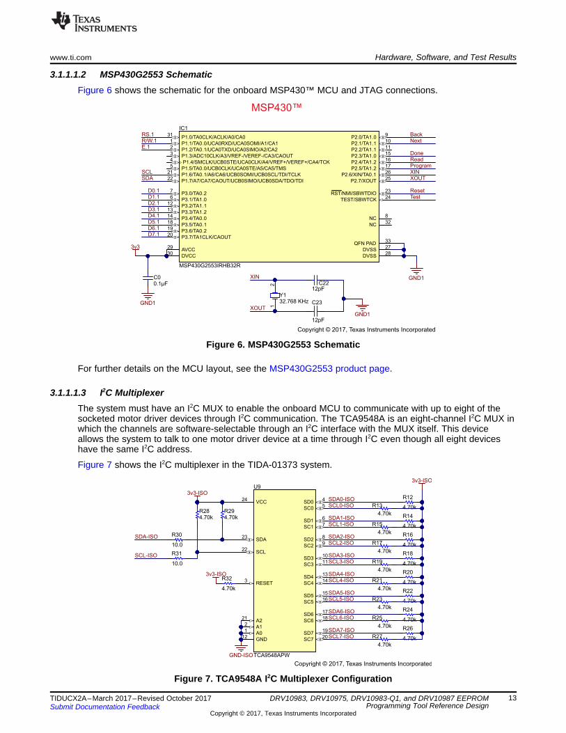
3.1.1.1.2 MSP430G2553 SchematicFigure 6 shows the schematic for the onboard MSP430™ MCU and JTAG connections.
Figure 6. MSP430G2553 Schematic
For further details on the MCU layout, see the MSP430G2553 product page.
3.1.1.1.3 I2C MultiplexerThe system must have an I2C MUX to enable the onboard MCU to communicate with up to eight of thesocketed motor driver devices through I2C communication. The TCA9548A is an eight-channel I2C MUX inwhich the channels are software-selectable through an I2C interface with the MUX itself. This deviceallows the system to talk to one motor driver device at a time through I2C even though all eight deviceshave the same I2C address.
Figure 7 shows the I2C multiplexer in the TIDA-01373 system.
Figure 7. TCA9548A I2C Multiplexer Configuration

LCD Module
VSS1
VDD2
VEE3
RS4
R/W5
E6
D07
D18
D29
D310
D4/D011
D5/D112
D6/D213
D7/D314
U11
EA DIPS082-HNLED
D0.2D1.2D2.2D3.2D4.2D5.2D6.2D7.2
GND1
5v
25k ohmR36
GND1
5v
Contrast
RS.2
R/W.2
E.2
0.1µFC27
1Y3
2Y6
3Y8
4Y11
1A2
1OE1
2OE4
2A5
3A9
3OE10
VCC14
4A12
4OE13
GND7
U12
SN74LV4T125PWR
1Y3
2Y6
3Y8
4Y11
1A2
1OE1
2OE4
2A5
3A9
3OE10
VCC14
4A12
4OE13
GND7
U13
SN74LV4T125PWR
1Y3
2Y6
3Y8
4Y11
1A2
1OE1
2OE4
2A5
3A9
3OE10
VCC14
4A12
4OE13
GND7
U14
SN74LV4T125PWR
GND1
GND1
GND1
GND1
GND1
GND1
5v
5v
D0.1D1.1D2.1D3.1
D4.1D5.1D6.1D7.1
RS.1R/W.1E.1
5v
D0.2D1.2D2.2D3.2
D4.2D5.2D6.2D7.2
RS.2R/W.2E.2
Copyright © 2017, Texas Instruments Incorporated
Hardware, Software, and Test Results www.ti.com
14 TIDUCX2A–March 2017–Revised October 2017Submit Documentation Feedback
Copyright © 2017, Texas Instruments Incorporated
DRV10983, DRV10975, DRV10983-Q1, and DRV10987 EEPROMProgramming Tool Reference Design
A typical application of the TCA9548A contains one or more data pullup voltages VDPUX: one for themaster device (VDPUM) and one for each of the selectable slave channels (VDPU0 through VDPU7). Inthe event where the master device and all slave devices operate at the same voltage, thenVDPUM = VDPUX = VCC. In an application where voltage translation is necessary, additional designrequirements must be considered to determine an appropriate VCC voltage. In the TIDA-01373 design,the user does not require voltage translation.
The A0, A1, and A2 pins are hardware selectable to control the slave address of the TCA9548A device.These pins can be tied directly to GND or VCC in the application. For the TIDA-01373, the user onlyutilizes one I2C multiplexer and therefore can select any combination; in this case, the designer chose topull all three of these pins to GND. If multiple slave channels are activated simultaneously in theapplication, then the total IOL from SCL/SDA to GND on the master side is the sum of the currentsthrough all the pullup resistors: 4.70-k resistors are used for the TIDA-01373. The DRV10983-Q1 devicerequires a 100-kHz I2C interface and therefore the pass-gate transistors of the TCA9548A are constructedsuch that the VCC voltage can be used to limit the maximum voltage that is passed from one I2C bus toanother [6].
3.1.1.1.4 LCD InterfaceFigure 8 shows the LCD schematic.
Figure 8. TIDA-01373 LCD Interface
Because the onboard LCD requires 5 V of power as well as logic, the TIDA-01373 incorporates three levelshifters in the design so that the MCU can properly communicate with the LCD.

Buttons
12 4
3
Back_button
12 4
3
Next_button
12 4
3
Done_button
12 4
3
Read_button
12 4
3
Program_button
0.1µFC5
0.1µFC6
0.1µFC8
0.1µFC9
0.1µFC10
GND1
47.0kR4
47.0kR5
47.0kR7
47.0kR8
47.0kR9
Back Next Done Read Program
3v3
Copyright © 2017, Texas Instruments Incorporated
www.ti.com Hardware, Software, and Test Results
15TIDUCX2A–March 2017–Revised October 2017Submit Documentation Feedback
Copyright © 2017, Texas Instruments Incorporated
DRV10983, DRV10975, DRV10983-Q1, and DRV10987 EEPROMProgramming Tool Reference Design
3.1.1.1.5 Button InterfaceFigure 9 shows the schematic layout of the GPIO buttons for the TIDA-01373 system.
Figure 9. Button Layout
The buttons for the system are open-drain (active low) logic. When a button is pressed, the input to theMCU is low. The RC time constant of the system can be calculated with the 0.1-µF capacitor and the47.0-kΩ resistor.
3.1.1.1.6 IsolationBecause the TIDA-01373 is a two-board solution and requires two separate power supplies, there is noguarantee that both power supplies will have the same ground reference. Due to this uncertainty, theTIDA-01373 has built-in isolation to prevent shoot-through and damage to either the DRV10983,DRV10975, DRV10983-Q1, or DRV10987 devices or the onboard MCU as well as all of the otherperipheral components. A second LP5907 LDO on the isolated side exists to provide a 3V3 rail, thecircuitry is the same as the previously mentioned LP5907 LDO.
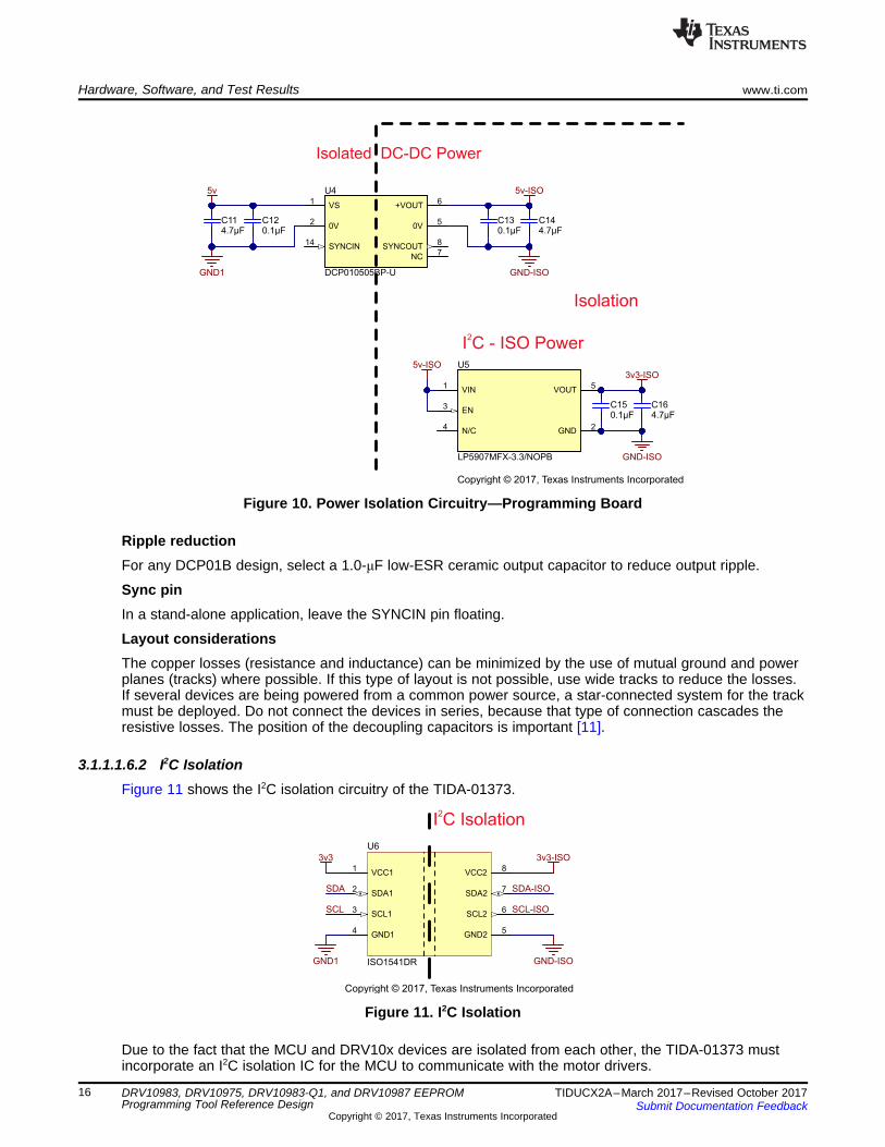
3.1.1.1.6.1 Power IsolationFigure 10 details the power isolation circuitry on the programming board.
I C Isolation2
VCC11
SDA12
SCL13
GND14
GND25
SCL26
SDA27
VCC28
U6
ISO1541DR
3v3
GND1
SDA
SCL
SDA-ISO
SCL-ISO
GND-ISO
3v3-ISO
Copyright © 2017, Texas Instruments Incorporated
VS1
0V2
0V5
+VOUT6
NC7
SYNCOUT8
SYNCIN14
U4
DCP010505BP-UGND1
5v
4.7µFC11
0.1µFC12
0.1µFC13
4.7µFC14
GND-ISO
5v-ISO
VIN1
GND2
EN3
N/C4
VOUT5
U5
LP5907MFX-3.3/NOPB
0.1µFC15
4.7µFC16
GND-ISO
3v3-ISO5v-ISO
Isolation
Isolated DC-DC Power
I C - ISO Power2
Copyright © 2017, Texas Instruments Incorporated
Hardware, Software, and Test Results www.ti.com
16 TIDUCX2A–March 2017–Revised October 2017Submit Documentation Feedback
Copyright © 2017, Texas Instruments Incorporated
DRV10983, DRV10975, DRV10983-Q1, and DRV10987 EEPROMProgramming Tool Reference Design
Figure 10. Power Isolation Circuitry—Programming Board
Ripple reductionFor any DCP01B design, select a 1.0-μF low-ESR ceramic output capacitor to reduce output ripple.
Sync pinIn a stand-alone application, leave the SYNCIN pin floating.
Layout considerationsThe copper losses (resistance and inductance) can be minimized by the use of mutual ground and powerplanes (tracks) where possible. If this type of layout is not possible, use wide tracks to reduce the losses.If several devices are being powered from a common power source, a star-connected system for the trackmust be deployed. Do not connect the devices in series, because that type of connection cascades theresistive losses. The position of the decoupling capacitors is important [11].
3.1.1.1.6.2 I2C IsolationFigure 11 shows the I2C isolation circuitry of the TIDA-01373.
Figure 11. I2C Isolation
Due to the fact that the MCU and DRV10x devices are isolated from each other, the TIDA-01373 mustincorporate an I2C isolation IC for the MCU to communicate with the motor drivers.
OUT DIODE
OUT IN Q DIODE
V VD
V V V V
+
=
+ - +
VIN8
DR6
PGND5
AGND4
ISEN1
FA/SD7
COMP2
FB3
U10
LM3478QMMX/NOPB
GND-TG
54.9kR2
887R3
0.27µFC5
4700pFC4
100
R4
0.013R5
1000pFC6
4
7,8
1,2
,3
5,6
,
FET2BSC340N08NS3 G
10.0kR7
4.7µF
C7 1
4
3
D1
50WQ10FNPBF
150µFC8
4.7µFC9
22µFC1
4.7µFC2
0.1µFC3
33µH
L1
120µH
L2
GND-TGVSource 24v
165kR6
GND-TG
10.0kRD1
Copyright © 2017, Texas Instruments Incorporated
www.ti.com Hardware, Software, and Test Results
17TIDUCX2A–March 2017–Revised October 2017Submit Documentation Feedback
Copyright © 2017, Texas Instruments Incorporated
DRV10983, DRV10975, DRV10983-Q1, and DRV10987 EEPROMProgramming Tool Reference Design
3.1.1.2 Socket BoardThe socket board consists of power management, the system ON and OFF logic, and eight sockets inwhich the DRV10983, DRV10975, DRV10983-Q1, and DRV10987 device is placed.
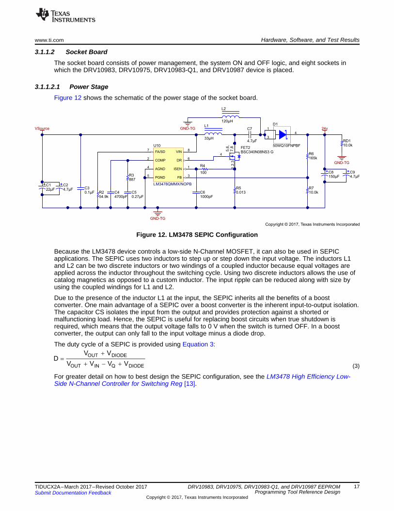
3.1.1.2.1 Power StageFigure 12 shows the schematic of the power stage of the socket board.
Figure 12. LM3478 SEPIC Configuration
Because the LM3478 device controls a low-side N-Channel MOSFET, it can also be used in SEPICapplications. The SEPIC uses two inductors to step up or step down the input voltage. The inductors L1and L2 can be two discrete inductors or two windings of a coupled inductor because equal voltages areapplied across the inductor throughout the switching cycle. Using two discrete inductors allows the use ofcatalog magnetics as opposed to a custom inductor. The input ripple can be reduced along with size byusing the coupled windings for L1 and L2.
Due to the presence of the inductor L1 at the input, the SEPIC inherits all the benefits of a boostconverter. One main advantage of a SEPIC over a boost converter is the inherent input-to-output isolation.The capacitor CS isolates the input from the output and provides protection against a shorted ormalfunctioning load. Hence, the SEPIC is useful for replacing boost circuits when true shutdown isrequired, which means that the output voltage falls to 0 V when the switch is turned OFF. In a boostconverter, the output can only fall to the input voltage minus a diode drop.
The duty cycle of a SEPIC is provided using Equation 3:
(3)
For greater detail on how to best design the SEPIC configuration, see the LM3478 High Efficiency Low-Side N-Channel Controller for Switching Reg [13].

ON/OFF
GND-TG
VSourceVin
6.04k
R0
4.02kR1
1
4
2,3,5,6,7
FET-NIRF1324S-7PPBF
0
RS
GND-TG
4
7,81,2,3
5,6,
FET-P
ECH8310-TL-H
10.0kRV
Copyright © 2017, Texas Instruments Incorporated
Hardware, Software, and Test Results www.ti.com
18 TIDUCX2A–March 2017–Revised October 2017Submit Documentation Feedback
Copyright © 2017, Texas Instruments Incorporated
DRV10983, DRV10975, DRV10983-Q1, and DRV10987 EEPROMProgramming Tool Reference Design
3.1.1.2.2 ON and OFF LogicFigure 13 shows the ON and OFF logic of the socket board.
Figure 13. Socket Board ON and OFF Logic
The ON and OFF logic on the socket board allows for the single ON and OFF switch located on theprogramming board to control the entire TIDA-01373 system.
When the ON and OFF switch on the programming board is in the ‘off’ state, the ON and OFF signal sentto the socket board is 0 V. The 0-V signal corresponds to the gate voltage of the N-Type FET in the ONand OFF logic of the socket board. The 0-V gate voltage on the N-Type FET turns the FET “off”, whichmeans that no current flows from VIN to GND-TG. This action, in turn, creates no voltage drop across theR0 and R1 resistors. With no voltage drop across these resistors, the gate voltage of the P-Type FET inthe logic is then pulled high to VIN. This high voltage on the P-Type FET turns this FET “off” as well, whichmeans that no current flows from VIN to GND-TG through the RV resistor. This action results in VSourcebeing pulled to GND-TG. The sockets on the socket board receive no power in this state.
When the ON and OFF switch on the programming board is in the ‘on’ state, the ON and OFF signal sentto the socket board is 5 V. The 5-V signal corresponds to the gate voltage of the N-Type FET in the ONand OFF login of the socket board. The 5-V gate voltage on the N-Type FET turns the FET “on”, whichmeans that the current now flows from VIN to GND-TG. When current flows from VIN to GND-TG across theR0 and R1 resistors there is a voltage drop. The R0 and R1 resistors act as a voltage divider for the gatevoltage for the P-Type FET in the systems logic. Now the voltage at the gate Vg is 40% of the VIN voltage,that is, Vg << VIN and the P-Type FET turns “on” and current flows from VIN to GND-TG through the RVresistor. Now VSource is approximate to VIN after subtracting a small voltage drop across the FET. In thisstate, the VSource feeds the LM3478 boost converter and the sockets now receive power.
1
2
3
4
5
6
7
8
9
10
11
12 13
14
15
16
17
18
19
20
21
22
23
24
EP
25
U1
GND-TG
0.1µF
C21
1µF
C51
1µF
C61
10µFC11
GND-TG
0.01µF
C31
47µH
L11
10µFC41
GND-TG
GND-TG
SCL1-TGSDA1-TG
F110452.500MRL
24v
3v3-1
4.70kR11
4.70kR21
GND-TG
3v3-1
1.00M
R01
GND-TG
4.70k
R41
4.70k
R313v3-1
4.70kR51
0.1µFC71
Copyright © 2017, Texas Instruments Incorporated
www.ti.com Hardware, Software, and Test Results
19TIDUCX2A–March 2017–Revised October 2017Submit Documentation Feedback
Copyright © 2017, Texas Instruments Incorporated
DRV10983, DRV10975, DRV10983-Q1, and DRV10987 EEPROMProgramming Tool Reference Design
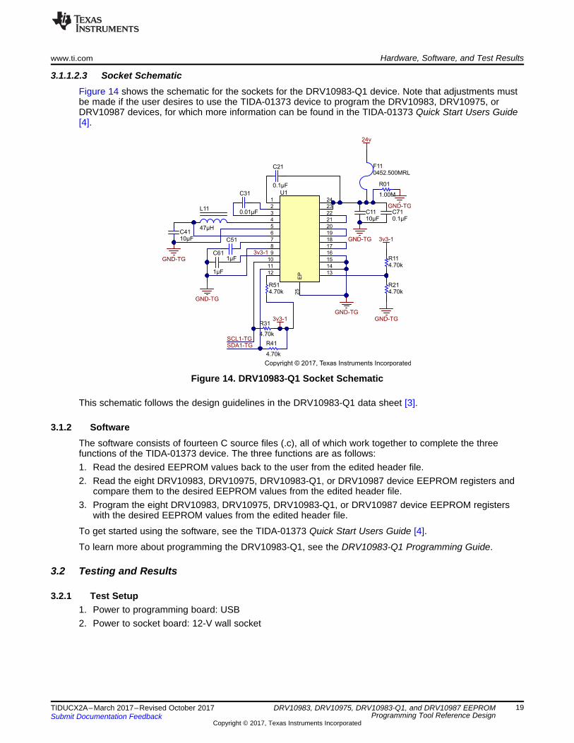
3.1.1.2.3 Socket SchematicFigure 14 shows the schematic for the sockets for the DRV10983-Q1 device. Note that adjustments mustbe made if the user desires to use the TIDA-01373 device to program the DRV10983, DRV10975, orDRV10987 devices, for which more information can be found in the TIDA-01373 Quick Start Users Guide[4].
Figure 14. DRV10983-Q1 Socket Schematic
This schematic follows the design guidelines in the DRV10983-Q1 data sheet [3].
3.1.2 SoftwareThe software consists of fourteen C source files (.c), all of which work together to complete the threefunctions of the TIDA-01373 device. The three functions are as follows:1. Read the desired EEPROM values back to the user from the edited header file.2. Read the eight DRV10983, DRV10975, DRV10983-Q1, or DRV10987 device EEPROM registers and
compare them to the desired EEPROM values from the edited header file.3. Program the eight DRV10983, DRV10975, DRV10983-Q1, or DRV10987 device EEPROM registers
with the desired EEPROM values from the edited header file.
To get started using the software, see the TIDA-01373 Quick Start Users Guide [4].
To learn more about programming the DRV10983-Q1, see the DRV10983-Q1 Programming Guide.
3.2 Testing and Results
3.2.1 Test Setup1. Power to programming board: USB2. Power to socket board: 12-V wall socket
Hardware, Software, and Test Results www.ti.com
20 TIDUCX2A–March 2017–Revised October 2017Submit Documentation Feedback
Copyright © 2017, Texas Instruments Incorporated
DRV10983, DRV10975, DRV10983-Q1, and DRV10987 EEPROMProgramming Tool Reference Design
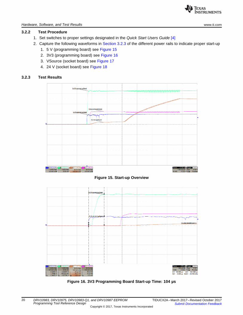
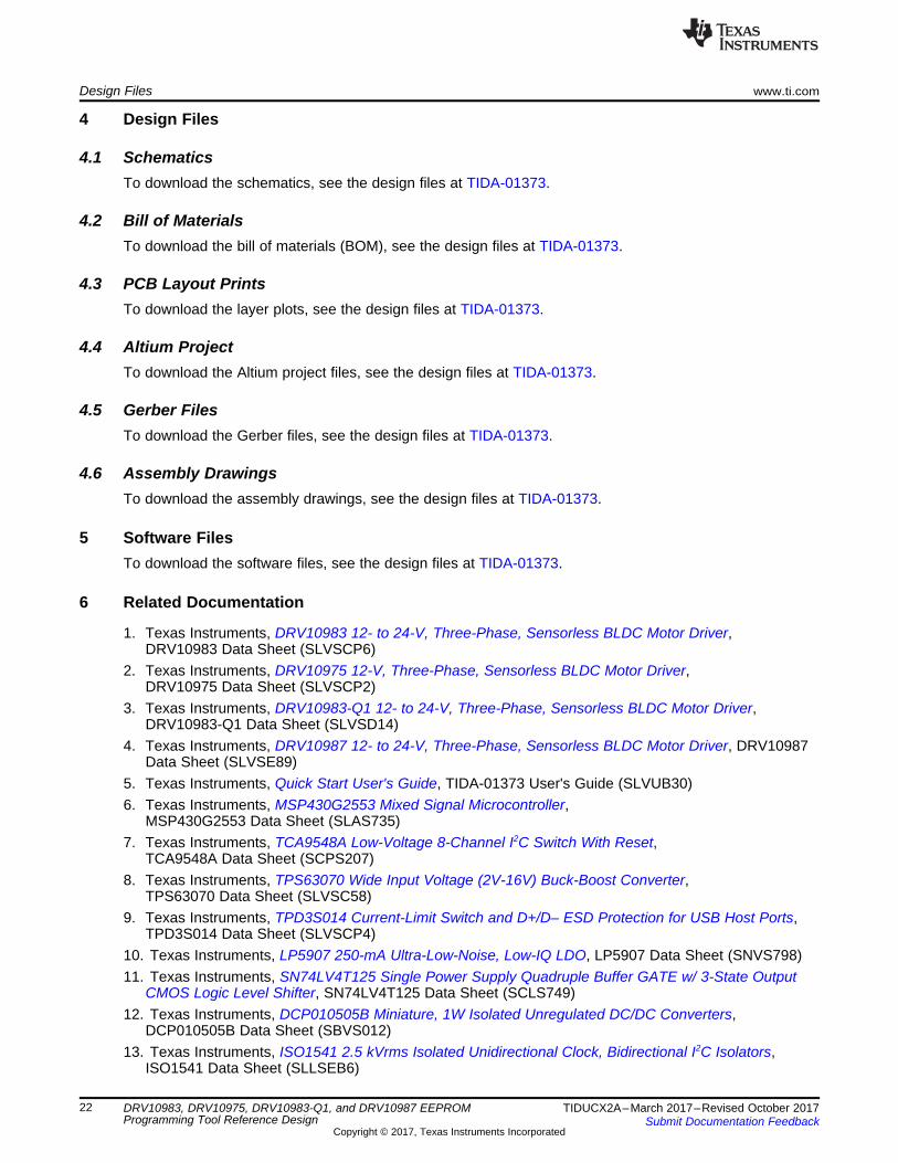
3.2.2 Test Procedure1. Set switches to proper settings designated in the Quick Start Users Guide [4]2. Capture the following waveforms in Section 3.2.3 of the different power rails to indicate proper start-up
1. 5 V (programming board) see Figure 152. 3V3 (programming board) see Figure 163. VSource (socket board) see Figure 174. 24 V (socket board) see Figure 18
3.2.3 Test Results
Figure 15. Start-up Overview
Figure 16. 3V3 Programming Board Start-up Time: 104 µs

www.ti.com Hardware, Software, and Test Results
21TIDUCX2A–March 2017–Revised October 2017Submit Documentation Feedback
Copyright © 2017, Texas Instruments Incorporated
DRV10983, DRV10975, DRV10983-Q1, and DRV10987 EEPROMProgramming Tool Reference Design
Figure 17. VSource Socket Board Start-up Time: 270 µs
Figure 18. 24-V Socket Board Startup Time: 6.24 ms
Design Files www.ti.com
22 TIDUCX2A–March 2017–Revised October 2017Submit Documentation Feedback
Copyright © 2017, Texas Instruments Incorporated
DRV10983, DRV10975, DRV10983-Q1, and DRV10987 EEPROMProgramming Tool Reference Design
4 Design Files
4.1 SchematicsTo download the schematics, see the design files at TIDA-01373.
4.2 Bill of MaterialsTo download the bill of materials (BOM), see the design files at TIDA-01373.
4.3 PCB Layout PrintsTo download the layer plots, see the design files at TIDA-01373.
4.4 Altium ProjectTo download the Altium project files, see the design files at TIDA-01373.
4.5 Gerber FilesTo download the Gerber files, see the design files at TIDA-01373.
4.6 Assembly DrawingsTo download the assembly drawings, see the design files at TIDA-01373.
5 Software FilesTo download the software files, see the design files at TIDA-01373.
6 Related Documentation
1. Texas Instruments, DRV10983 12- to 24-V, Three-Phase, Sensorless BLDC Motor Driver,DRV10983 Data Sheet (SLVSCP6)
2. Texas Instruments, DRV10975 12-V, Three-Phase, Sensorless BLDC Motor Driver,DRV10975 Data Sheet (SLVSCP2)
3. Texas Instruments, DRV10983-Q1 12- to 24-V, Three-Phase, Sensorless BLDC Motor Driver,DRV10983-Q1 Data Sheet (SLVSD14)
4. Texas Instruments, DRV10987 12- to 24-V, Three-Phase, Sensorless BLDC Motor Driver, DRV10987Data Sheet (SLVSE89)
5. Texas Instruments, Quick Start User's Guide, TIDA-01373 User's Guide (SLVUB30)6. Texas Instruments, MSP430G2553 Mixed Signal Microcontroller,
MSP430G2553 Data Sheet (SLAS735)7. Texas Instruments, TCA9548A Low-Voltage 8-Channel I2C Switch With Reset,
TCA9548A Data Sheet (SCPS207)8. Texas Instruments, TPS63070 Wide Input Voltage (2V-16V) Buck-Boost Converter,
TPS63070 Data Sheet (SLVSC58)9. Texas Instruments, TPD3S014 Current-Limit Switch and D+/D– ESD Protection for USB Host Ports,
TPD3S014 Data Sheet (SLVSCP4)10. Texas Instruments, LP5907 250-mA Ultra-Low-Noise, Low-IQ LDO, LP5907 Data Sheet (SNVS798)11. Texas Instruments, SN74LV4T125 Single Power Supply Quadruple Buffer GATE w/ 3-State Output
CMOS Logic Level Shifter, SN74LV4T125 Data Sheet (SCLS749)12. Texas Instruments, DCP010505B Miniature, 1W Isolated Unregulated DC/DC Converters,
DCP010505B Data Sheet (SBVS012)13. Texas Instruments, ISO1541 2.5 kVrms Isolated Unidirectional Clock, Bidirectional I2C Isolators,
ISO1541 Data Sheet (SLLSEB6)

www.ti.com Terminology
23TIDUCX2A–March 2017–Revised October 2017Submit Documentation Feedback
Copyright © 2017, Texas Instruments Incorporated
DRV10983, DRV10975, DRV10983-Q1, and DRV10987 EEPROMProgramming Tool Reference Design
14. Texas Instruments, LM3478x/-Q1 High-Efficiency Low-Side N-Channel Controller for SwitchingRegulator, LM3478/LM3478Q-Q1 Data Sheet (SNVS085)
15. Texas Instruments, TPD8E003 8-Channel ESD Array For Portable Space-Saving Applications,TPD8E003 Data Sheet (SLLSE38)
6.1 TrademarksMSP430 is a trademark of Texas Instruments.
7 TerminologyADC— Analog-to-digital converter
BLDC— Brushless DC
DCO— Digitally-controlled oscillator
EEPROM — Electrically erasable programmable read-only memory
ESD— Electrostatic discharge
ESR— Equivalent series resistance
GPIO — General port input output
GND— Ground
JTAG— Joint Test Action Group
LDO— Linear dropout regulator
MOSFET— Metal-oxide-semiconductor field-effect transistor
MCU— Microcontroller
MUX— Multiplexer
PWM— Pulse-width modulation
TVS— Transient voltage suppressor
USB— Universal serial bus
8 About the AuthorMICHAEL THOMAS SCHNEIDER is a Motor Driver Applications Associate in the Applications RotationProgram at Texas Instruments, where he is responsible for developing reference design solutions andsupporting the DRV10x family of devices. Michael brings to this team his knowledge of mixed signalsystem level designs as well as electric motor drives in order to continue to build collateral material for theDRV10x family. Michael earned his Bachelor of Science in Electrical Engineering (BSEE) at the Universityof Texas at Austin.

Revision History www.ti.com
24 TIDUCX2A–March 2017–Revised October 2017Submit Documentation Feedback
Copyright © 2017, Texas Instruments Incorporated
Revision History
Revision HistoryNOTE: Page numbers for previous revisions may differ from page numbers in the current version.
Changes from Original (March 2017) to A Revision ....................................................................................................... Page
• Updated title from DRV10983, DRV10975, and DRV10983Q1 EEPROM Programming Tool Reference Design toDRV10983, DRV10975, DRV10983-Q1, and DRV10987 EEPROM Programming Tool Reference Design ................. 1
• Added DRV10987 to Resources and to overall design to complement DRV10983, DRV10983-Q1, and DRV10975 ...... 1• Added DRV10987 to Highlighted Products ............................................................................................ 5• Added DRV10987 data sheet (SLVSE89) to Related Documentation............................................................ 22
IMPORTANT NOTICE FOR TI DESIGN INFORMATION AND RESOURCES
Texas Instruments Incorporated (‘TI”) technical, application or other design advice, services or information, including, but not limited to,reference designs and materials relating to evaluation modules, (collectively, “TI Resources”) are intended to assist designers who aredeveloping applications that incorporate TI products; by downloading, accessing or using any particular TI Resource in any way, you(individually or, if you are acting on behalf of a company, your company) agree to use it solely for this purpose and subject to the terms ofthis Notice.TI’s provision of TI Resources does not expand or otherwise alter TI’s applicable published warranties or warranty disclaimers for TIproducts, and no additional obligations or liabilities arise from TI providing such TI Resources. TI reserves the right to make corrections,enhancements, improvements and other changes to its TI Resources.You understand and agree that you remain responsible for using your independent analysis, evaluation and judgment in designing yourapplications and that you have full and exclusive responsibility to assure the safety of your applications and compliance of your applications(and of all TI products used in or for your applications) with all applicable regulations, laws and other applicable requirements. Yourepresent that, with respect to your applications, you have all the necessary expertise to create and implement safeguards that (1)anticipate dangerous consequences of failures, (2) monitor failures and their consequences, and (3) lessen the likelihood of failures thatmight cause harm and take appropriate actions. You agree that prior to using or distributing any applications that include TI products, youwill thoroughly test such applications and the functionality of such TI products as used in such applications. TI has not conducted anytesting other than that specifically described in the published documentation for a particular TI Resource.You are authorized to use, copy and modify any individual TI Resource only in connection with the development of applications that includethe TI product(s) identified in such TI Resource. NO OTHER LICENSE, EXPRESS OR IMPLIED, BY ESTOPPEL OR OTHERWISE TOANY OTHER TI INTELLECTUAL PROPERTY RIGHT, AND NO LICENSE TO ANY TECHNOLOGY OR INTELLECTUAL PROPERTYRIGHT OF TI OR ANY THIRD PARTY IS GRANTED HEREIN, including but not limited to any patent right, copyright, mask work right, orother intellectual property right relating to any combination, machine, or process in which TI products or services are used. Informationregarding or referencing third-party products or services does not constitute a license to use such products or services, or a warranty orendorsement thereof. Use of TI Resources may require a license from a third party under the patents or other intellectual property of thethird party, or a license from TI under the patents or other intellectual property of TI.TI RESOURCES ARE PROVIDED “AS IS” AND WITH ALL FAULTS. TI DISCLAIMS ALL OTHER WARRANTIES ORREPRESENTATIONS, EXPRESS OR IMPLIED, REGARDING TI RESOURCES OR USE THEREOF, INCLUDING BUT NOT LIMITED TOACCURACY OR COMPLETENESS, TITLE, ANY EPIDEMIC FAILURE WARRANTY AND ANY IMPLIED WARRANTIES OFMERCHANTABILITY, FITNESS FOR A PARTICULAR PURPOSE, AND NON-INFRINGEMENT OF ANY THIRD PARTY INTELLECTUALPROPERTY RIGHTS.TI SHALL NOT BE LIABLE FOR AND SHALL NOT DEFEND OR INDEMNIFY YOU AGAINST ANY CLAIM, INCLUDING BUT NOTLIMITED TO ANY INFRINGEMENT CLAIM THAT RELATES TO OR IS BASED ON ANY COMBINATION OF PRODUCTS EVEN IFDESCRIBED IN TI RESOURCES OR OTHERWISE. IN NO EVENT SHALL TI BE LIABLE FOR ANY ACTUAL, DIRECT, SPECIAL,COLLATERAL, INDIRECT, PUNITIVE, INCIDENTAL, CONSEQUENTIAL OR EXEMPLARY DAMAGES IN CONNECTION WITH ORARISING OUT OF TI RESOURCES OR USE THEREOF, AND REGARDLESS OF WHETHER TI HAS BEEN ADVISED OF THEPOSSIBILITY OF SUCH DAMAGES.You agree to fully indemnify TI and its representatives against any damages, costs, losses, and/or liabilities arising out of your non-compliance with the terms and provisions of this Notice.This Notice applies to TI Resources. Additional terms apply to the use and purchase of certain types of materials, TI products and services.These include; without limitation, TI’s standard terms for semiconductor products http://www.ti.com/sc/docs/stdterms.htm), evaluationmodules, and samples (http://www.ti.com/sc/docs/sampterms.htm).
Mailing Address: Texas Instruments, Post Office Box 655303, Dallas, Texas 75265Copyright © 2017, Texas Instruments Incorporated