ds2490 usb to 1-wire bridge chip - isens.ruisens.ru/files/ds2490.pdfthe ds2490 is a bridge chip that...
TRANSCRIPT

1 of 50 120401
FEATURES� Communicates at regular and overdrive 1-
Wire® speeds� Supports 12V EPROM programming and stiff
5V pullup for EEPROM, sensors, and cryptoiButton®
� Slew rate controlled 1-Wire timing and activepullup to accommodate long 1-Wire networklines and reduce radiation
� Programmable 1-Wire timing and drivercharacteristics accommodate a wide range of1-Wire network configurations
� Low- to high-level command types, includingmacros, for generating 1-Wire communication
� Crystal oscillator timebase provides precisiontimed 1-Wire waveforms
� High-speed 12Mbps Universal Serial Bus(USB) interface
� Integrated USB-compliant transceiver� Supports USB remote wake-up from a 1-Wire
device event to resume a suspended hostsystem
� 0oC to +70oC operating temperature range
PIN ASSIGNMENT24-Pin SOTop View (300-mil)
VD
NC
NC
NC
XI
XO
NC
VPP
NC
NC
NC
1-WIRE
PMOD
NC
VB
NCNC
NC
NC
NC
D-
D+
GND
1
2
3
4
5
6
7
8
9
10
11
12 13
14
15
16
1718
19
20
21
22
23
24
SUSO
Flip-Chip Package, Top View
A4
NC
B4 C4 D4
A3 B3 E3
A2 C2
D1
E2
NC SUSO\ D-
D+PMODNC
XI
NCNC
7.1 mm
4.4 mm
NC
A1
NC
F4
NC
F3
F2
1W
NC
F1
NC
G4
NC
G3
G2
NC
NC
G1
NC
B2
B1
VDD
NC
C3
C1
VB
XO
E4
GND
E1
VPP
ORDERING INFORMATIONPART NUMBER PACKAGE DESCRIPTION
DS2490S 24-pin SO
DS2490S/T&R Tape & Reel of DS2490S
DS2490X Flip-Chip Package, Tape & Reel
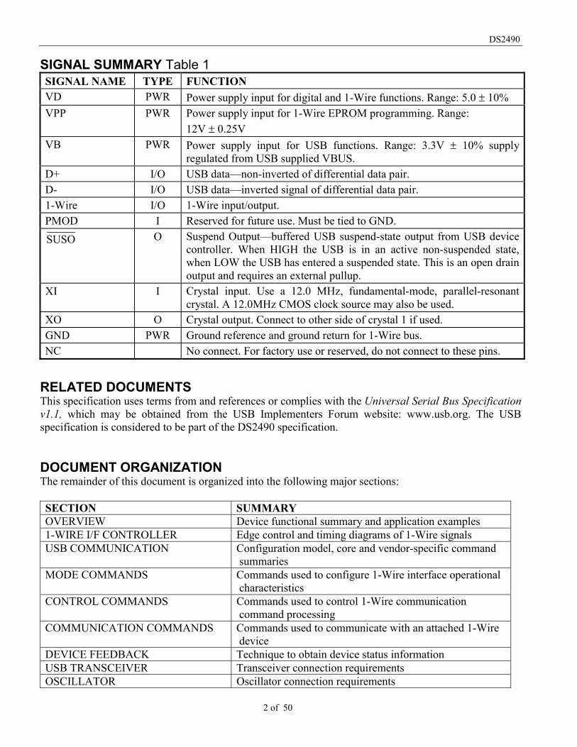
DESCRIPTIONThe DS2490 is a bridge chip that enables communication between a USB host system and a 1-Wire bus.It provides regular, overdrive, and flexible 1-Wire communication speeds and a full-speed 12Mbpsconnection to USB. USB vendor-specific commands defined in this specification are used to control theDS2490 and communicate with attached 1-Wire devices. A functional block diagram of the DS2490 isshown in Figure 1.
DS2490USB to 1-Wire Bridge Chip
www.maxim-ic.com
DS2490
2 of 50
SIGNAL SUMMARY Table 1SIGNAL NAME TYPE FUNCTIONVD PWR Power supply input for digital and 1-Wire functions. Range: 5.0 � 10%VPP PWR Power supply input for 1-Wire EPROM programming. Range:
12V � 0.25VVB PWR Power supply input for USB functions. Range: 3.3V � 10% supply
regulated from USB supplied VBUS.D+ I/O USB data—non-inverted of differential data pair.D- I/O USB data—inverted signal of differential data pair.1-Wire I/O 1-Wire input/output.PMOD I Reserved for future use. Must be tied to GND.SUSO O Suspend Output—buffered USB suspend-state output from USB device
controller. When HIGH the USB is in an active non-suspended state,when LOW the USB has entered a suspended state. This is an open drainoutput and requires an external pullup.
XI I Crystal input. Use a 12.0 MHz, fundamental-mode, parallel-resonantcrystal. A 12.0MHz CMOS clock source may also be used.
XO O Crystal output. Connect to other side of crystal 1 if used.GND PWR Ground reference and ground return for 1-Wire bus.NC No connect. For factory use or reserved, do not connect to these pins.
RELATED DOCUMENTSThis specification uses terms from and references or complies with the Universal Serial Bus Specificationv1.1, which may be obtained from the USB Implementers Forum website: www.usb.org. The USBspecification is considered to be part of the DS2490 specification.
DOCUMENT ORGANIZATIONThe remainder of this document is organized into the following major sections:
SECTION SUMMARYOVERVIEW Device functional summary and application examples1-WIRE I/F CONTROLLER Edge control and timing diagrams of 1-Wire signalsUSB COMMUNICATION Configuration model, core and vendor-specific command
summariesMODE COMMANDS Commands used to configure 1-Wire interface operational
characteristicsCONTROL COMMANDS Commands used to control 1-Wire communication
command processingCOMMUNICATION COMMANDS Commands used to communicate with an attached 1-Wire
deviceDEVICE FEEDBACK Technique to obtain device status informationUSB TRANSCEIVER Transceiver connection requirementsOSCILLATOR Oscillator connection requirements
DS2490
3 of 50
SECTION SUMMARYSUSPEND OUTPUT SUSO signal operation and purposeELECTRICAL CHARACTERISTICS DC and AC specificationsAPPLICATION INFORMATION HW application exampleAPPENDIX 1 CONTROL COMMANDS—USB setup packet encodingAPPENDIX 2 COMMUNICATION COMMANDS—USB setup packet
encodingAPPENDIX 3 MODE COMMANDS—USB setup packet encodingAPPENDIX 4 USB command and command type constant codes
OVERVIEWThe DS2490 directly interfaces a USB port to a 1-Wire bus. As shown in Figure 1, the DS2490incorporates a USB physical interface, a USB device controller coupled with a 1-Wire-specific USBfunction core, and a 1-Wire bus interface controller. The 1-Wire interface controller shapes the slopes ofthe 1-Wire waveforms, applies programming pulses or strong pullup to 5V, and reads the 1-Wire bususing a non-TTL threshold to maximize the noise margin for best performance on large 1-Wire Networks.1-Wire waveform timing is accurately controlled with a crystal-based oscillator.
The DS2490 also supports USB remote wake-up which enables the DS2490-based USB peripheral tosend resume signaling to a suspended host system. If the remote wake-up function is enabled and the hostsystem is in a suspended state, a 1-Wire device attachment will cause the DS2490 to perform a hostsystem wake-up and allow the 1-Wire device to be serviced.
DS2490 FUNCTIONAL BLOCK DIAGRAM Figure 1
USBXCVR
USBDEVICE
CONTROLLER
PWRCNTL
USB1-WIRE
FUNCTION CORE
EPFIFOS
OSC CLKGEN
USBDESCROM
1-WIREI/F
CONTROLLER1-WIRE
XI VPPXO
D+D-
VB
VD GND
SUSO
Typical application examples of the DS2490 are shown in Figure 2 (a to c). As shown in all the examples,all host control and communication with the device is accomplished over a USB communication link. AUSB vendor-specific command set, as defined in this document, is used to select operational modes(MODE COMMANDS), control command processing (CONTROL COMMANDS), and communicateover the 1-Wire interface (COMMUNICATION COMMANDS). Shown in Figure 2, example (a) is aDS2490-based USB peripheral application. The peripheral function is a USB to 1-Wire adapter andprovides both USB and 1-Wire I/O connections. In this example, the peripheral is attached to the USBenabled host computer either directly at a root port or through a USB hub. The 1-Wire bus interface

DS2490
4 of 50
provided by the DS2490 supports all 1-Wire devices manufactured by Dallas Semiconductor as well asthe various 1-Wire bus topologies simple multi-drop to complex 1-Wire Network. Example (b) and (c) inFigure 2 are variations of example (a) in which the DS2490 is embedded in the host computer or a USBHUB.
DS2490 APPLICATION EXAMPLES Figure 2
1-WIRE INTERFACE CONTROLLER1-Wire communication commands sent to the DS2490 are ultimately processed by the 1-Wire interfacecontroller. One of the tasks of the interface controller is to actively shape the edges of the 1-Wirecommunication waveforms. This speeds up the recharging of the 1-Wire bus (rising edges) and reducesringing of long lines (falling edges). The circuitry for shaping rising edges is always active. The slew rateof falling edges is actively controlled only at flexible speed and requires the parameter for slew ratecontrol being different from its power-on default value. See the MODE COMMANDS section forparameter control and power-on defaults.
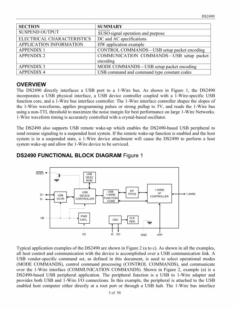
All Rising EdgesThe active pullup of the rising edges reduces the rise time on the 1-Wire bus significantly compared to asimple resistive pullup. Figure 3 shows how the DS2490 is involved in shaping a rising edge.
DS2490
5 of 50
ACTIVE PULLUP Figure 3
5V
0V
1-Wire busis discharged
VIAPO
VIAPTO
tAPUOT
t1 t2 t3
The circuit operates as follows: At t1, the pulldown (induced by the DS2490 or a device on the bus) ends.From this point on the 1-Wire bus is pulled high by the weak pullup current IWEAKPU provided by theDS2490. The slope is determined by the load on the bus and the value of the pullup current. At t2, thevoltage crosses the threshold voltage VIAPO. Now, the DS2490 switches over from the weak pullupcurrent IWEAKPU to the higher current IACTPU. As a consequence, the voltage on the bus now rises faster.As the voltage on the bus crosses the threshold VIAPTO at t3, a timer is started. As long as this timer is on(tAPUOT), the IACTPU current will continue to flow. After the timer is expired, the DS2490 will switch backto the weak pullup current.
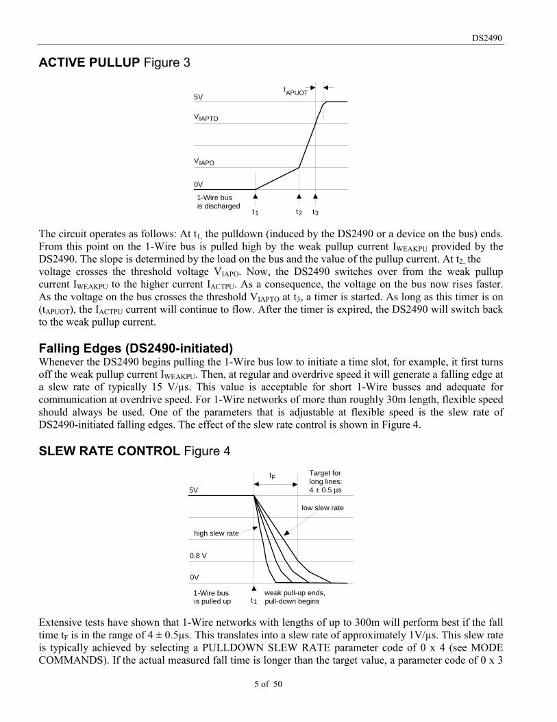
Falling Edges (DS2490-initiated)Whenever the DS2490 begins pulling the 1-Wire bus low to initiate a time slot, for example, it first turnsoff the weak pullup current IWEAKPU. Then, at regular and overdrive speed it will generate a falling edge ata slew rate of typically 15 V/µs. This value is acceptable for short 1-Wire busses and adequate forcommunication at overdrive speed. For 1-Wire networks of more than roughly 30m length, flexible speedshould always be used. One of the parameters that is adjustable at flexible speed is the slew rate ofDS2490-initiated falling edges. The effect of the slew rate control is shown in Figure 4.
SLEW RATE CONTROL Figure 4
5V
0V
0.8 V
tF
low slew rate
high slew rate
pull-down beginsweak pull-up ends,1-Wire bus
is pulled up
Target forlong lines:4 ± 0.5 µs
t1
Extensive tests have shown that 1-Wire networks with lengths of up to 300m will perform best if the falltime tF is in the range of 4 ± 0.5µs. This translates into a slew rate of approximately 1V/µs. This slew rateis typically achieved by selecting a PULLDOWN SLEW RATE parameter code of 0 x 4 (see MODECOMMANDS). If the actual measured fall time is longer than the target value, a parameter code of 0 x 3
DS2490
6 of 50
or lower should be used. If the fall time is shorter, a parameter code of 0x5 or higher should be used.Once determined, the value code for the PULLDOWN SLEW RATE control parameter should be storedin the host and always be loaded into the DS2490 after a power-on or master reset cycle.
1-WIRE TIMING DIAGRAMSThis section explains the 1-Wire bus waveforms generated by the DS2490. First, the communicationwaveforms such as the reset/presence detect sequence and read/write data time slots are discussedfollowed by a detailed description of the Pulse function under various conditions.
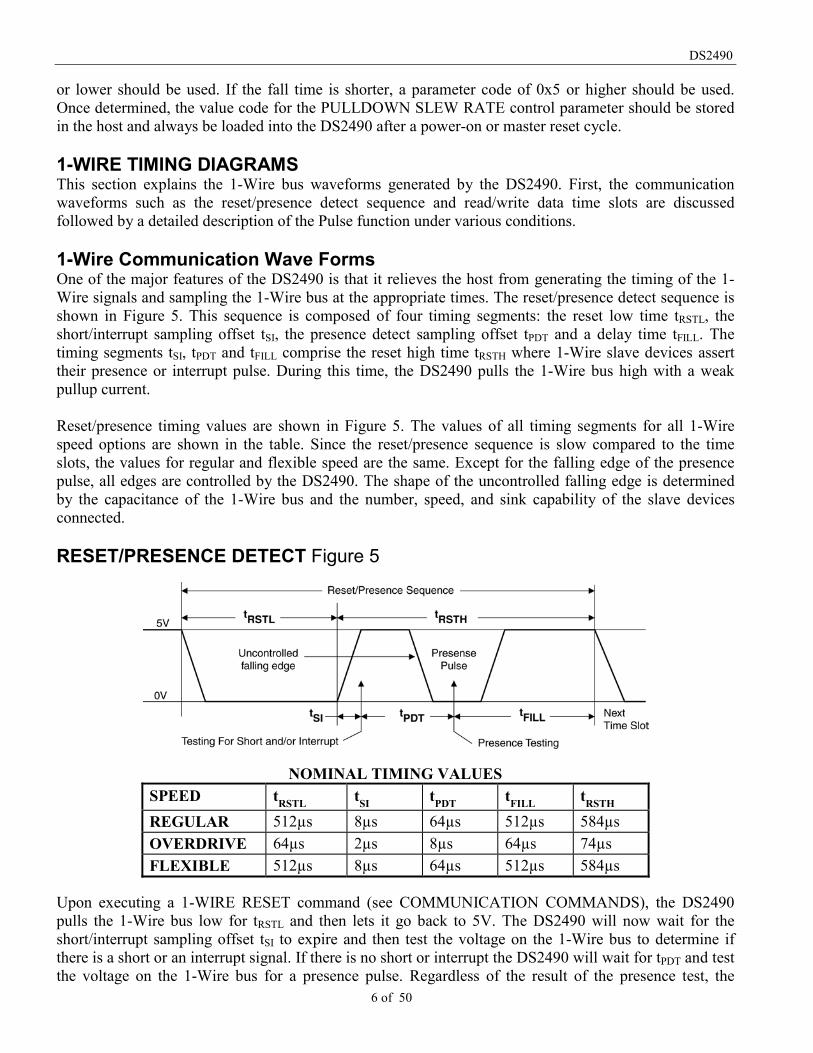
1-Wire Communication Wave FormsOne of the major features of the DS2490 is that it relieves the host from generating the timing of the 1-Wire signals and sampling the 1-Wire bus at the appropriate times. The reset/presence detect sequence isshown in Figure 5. This sequence is composed of four timing segments: the reset low time tRSTL, theshort/interrupt sampling offset tSI, the presence detect sampling offset tPDT and a delay time tFILL. Thetiming segments tSI, tPDT and tFILL comprise the reset high time tRSTH where 1-Wire slave devices asserttheir presence or interrupt pulse. During this time, the DS2490 pulls the 1-Wire bus high with a weakpullup current.
Reset/presence timing values are shown in Figure 5. The values of all timing segments for all 1-Wirespeed options are shown in the table. Since the reset/presence sequence is slow compared to the timeslots, the values for regular and flexible speed are the same. Except for the falling edge of the presencepulse, all edges are controlled by the DS2490. The shape of the uncontrolled falling edge is determinedby the capacitance of the 1-Wire bus and the number, speed, and sink capability of the slave devicesconnected.
RESET/PRESENCE DETECT Figure 5
NOMINAL TIMING VALUESSPEED tRSTL tSI tPDT tFILL tRSTH
REGULAR 512µs 8µs 64µs 512µs 584µsOVERDRIVE 64µs 2µs 8µs 64µs 74µsFLEXIBLE 512µs 8µs 64µs 512µs 584µs
Upon executing a 1-WIRE RESET command (see COMMUNICATION COMMANDS), the DS2490pulls the 1-Wire bus low for tRSTL and then lets it go back to 5V. The DS2490 will now wait for theshort/interrupt sampling offset tSI to expire and then test the voltage on the 1-Wire bus to determine ifthere is a short or an interrupt signal. If there is no short or interrupt the DS2490 will wait for tPDT and testthe voltage on the 1-Wire bus for a presence pulse. Regardless of the result of the presence test, the
DS2490
7 of 50
DS2490 will then wait for tFILL to expire and then, depending on the value of embedded 1-WIRE RESETcommand bits PST, NTF, and ICP, generate a command response byte that is available to the host.
If the test for interrupt or short reveals a logic 0, the DS2490 will wait for 4096µs and then test the 1-Wire bus again. If a logic 0 is detected, the 1-Wire bus is shorted and the DS2490 feedback response forthe 1-WIRE RESET communication command will indicate a short detection. If a logic 1 is detected, thedevice will wait for tFILL to expire, after which it will load the feedback response value for the 1-WIRERESET command with an alarming presence pulse detect value. See the DEVICE FEEDBACK sectionfor additional details. No additional testing for a presence pulse will be done. The DS2490 will performthe short/interrupt testing as described also at overdrive speed, although interrupt signaling is onlydefined for regular speed.
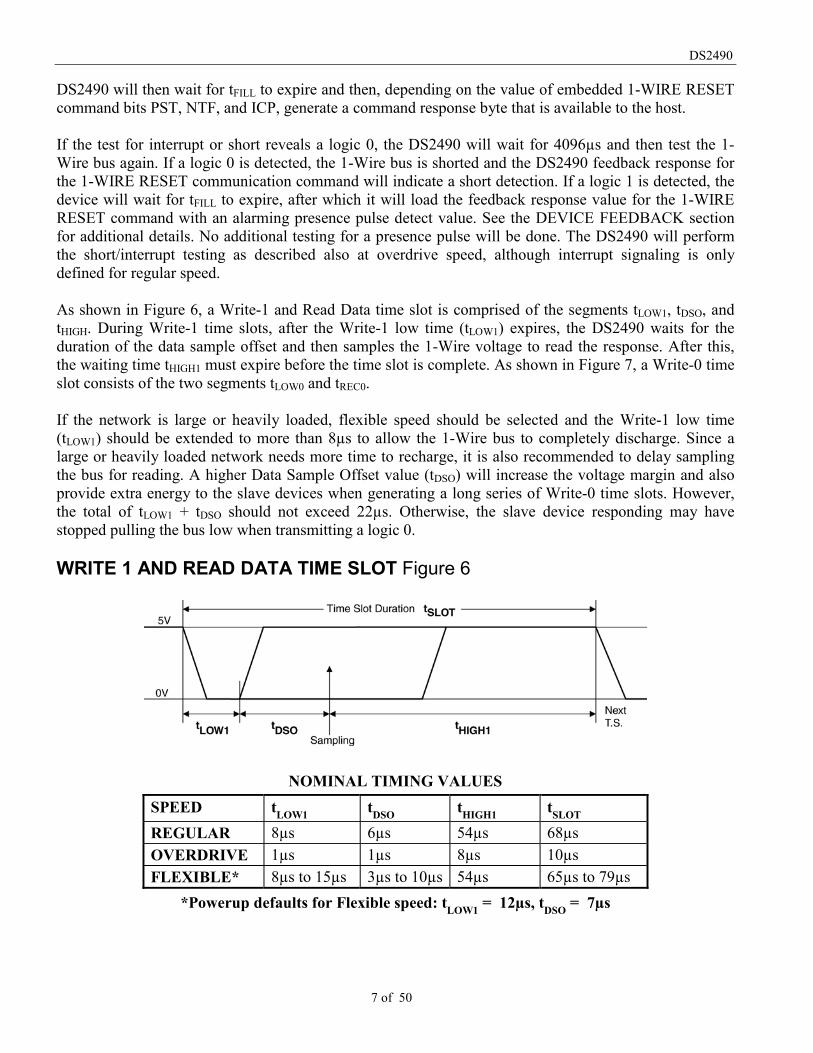
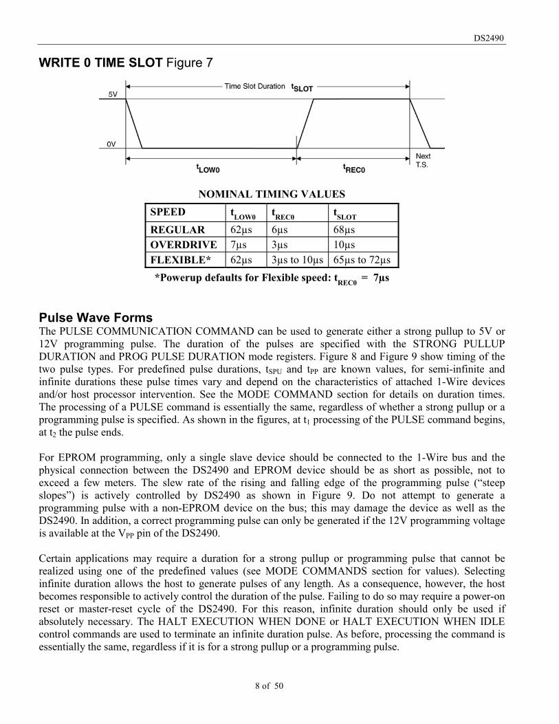
As shown in Figure 6, a Write-1 and Read Data time slot is comprised of the segments tLOW1, tDSO, andtHIGH. During Write-1 time slots, after the Write-1 low time (tLOW1) expires, the DS2490 waits for theduration of the data sample offset and then samples the 1-Wire voltage to read the response. After this,the waiting time tHIGH1 must expire before the time slot is complete. As shown in Figure 7, a Write-0 timeslot consists of the two segments tLOW0 and tREC0.
If the network is large or heavily loaded, flexible speed should be selected and the Write-1 low time(tLOW1) should be extended to more than 8µs to allow the 1-Wire bus to completely discharge. Since alarge or heavily loaded network needs more time to recharge, it is also recommended to delay samplingthe bus for reading. A higher Data Sample Offset value (tDSO) will increase the voltage margin and alsoprovide extra energy to the slave devices when generating a long series of Write-0 time slots. However,the total of tLOW1 + tDSO should not exceed 22µs. Otherwise, the slave device responding may havestopped pulling the bus low when transmitting a logic 0.
WRITE 1 AND READ DATA TIME SLOT Figure 6
NOMINAL TIMING VALUESSPEED tLOW1 tDSO tHIGH1 tSLOT
REGULAR 8µs 6µs 54µs 68µsOVERDRIVE 1µs 1µs 8µs 10µsFLEXIBLE* 8µs to 15µs 3µs to 10µs 54µs 65µs to 79µs
*Powerup defaults for Flexible speed: tLOW1 = 12µs, tDSO = 7µs
DS2490
8 of 50
WRITE 0 TIME SLOT Figure 7
NOMINAL TIMING VALUESSPEED tLOW0 tREC0 tSLOT
REGULAR 62µs 6µs 68µsOVERDRIVE 7µs 3µs 10µsFLEXIBLE* 62µs 3µs to 10µs 65µs to 72µs*Powerup defaults for Flexible speed: tREC0 = 7µs
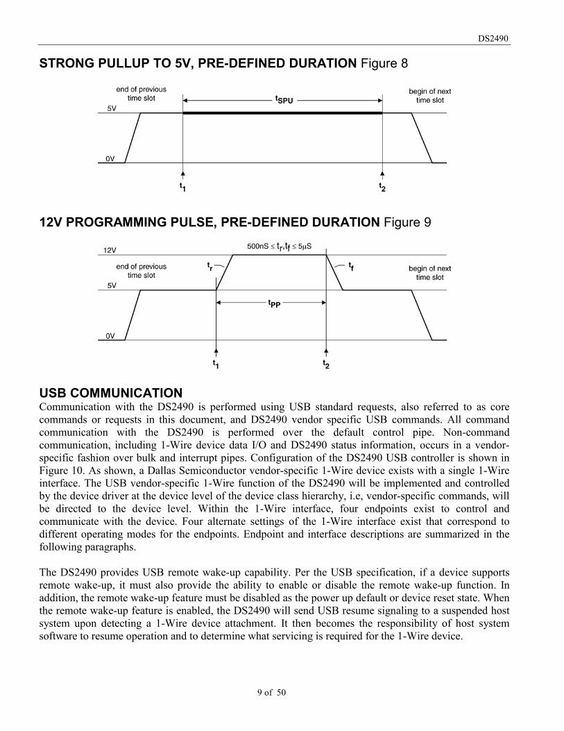
Pulse Wave FormsThe PULSE COMMUNICATION COMMAND can be used to generate either a strong pullup to 5V or12V programming pulse. The duration of the pulses are specified with the STRONG PULLUPDURATION and PROG PULSE DURATION mode registers. Figure 8 and Figure 9 show timing of thetwo pulse types. For predefined pulse durations, tSPU and tPP are known values, for semi-infinite andinfinite durations these pulse times vary and depend on the characteristics of attached 1-Wire devicesand/or host processor intervention. See the MODE COMMAND section for details on duration times.The processing of a PULSE command is essentially the same, regardless of whether a strong pullup or aprogramming pulse is specified. As shown in the figures, at t1 processing of the PULSE command begins,at t2 the pulse ends.
For EPROM programming, only a single slave device should be connected to the 1-Wire bus and thephysical connection between the DS2490 and EPROM device should be as short as possible, not toexceed a few meters. The slew rate of the rising and falling edge of the programming pulse (“steepslopes”) is actively controlled by DS2490 as shown in Figure 9. Do not attempt to generate aprogramming pulse with a non-EPROM device on the bus; this may damage the device as well as theDS2490. In addition, a correct programming pulse can only be generated if the 12V programming voltageis available at the VPP pin of the DS2490.
Certain applications may require a duration for a strong pullup or programming pulse that cannot berealized using one of the predefined values (see MODE COMMANDS section for values). Selectinginfinite duration allows the host to generate pulses of any length. As a consequence, however, the hostbecomes responsible to actively control the duration of the pulse. Failing to do so may require a power-onreset or master-reset cycle of the DS2490. For this reason, infinite duration should only be used ifabsolutely necessary. The HALT EXECUTION WHEN DONE or HALT EXECUTION WHEN IDLEcontrol commands are used to terminate an infinite duration pulse. As before, processing the command isessentially the same, regardless if it is for a strong pullup or a programming pulse.
DS2490
9 of 50
STRONG PULLUP TO 5V, PRE-DEFINED DURATION Figure 8
12V PROGRAMMING PULSE, PRE-DEFINED DURATION Figure 9
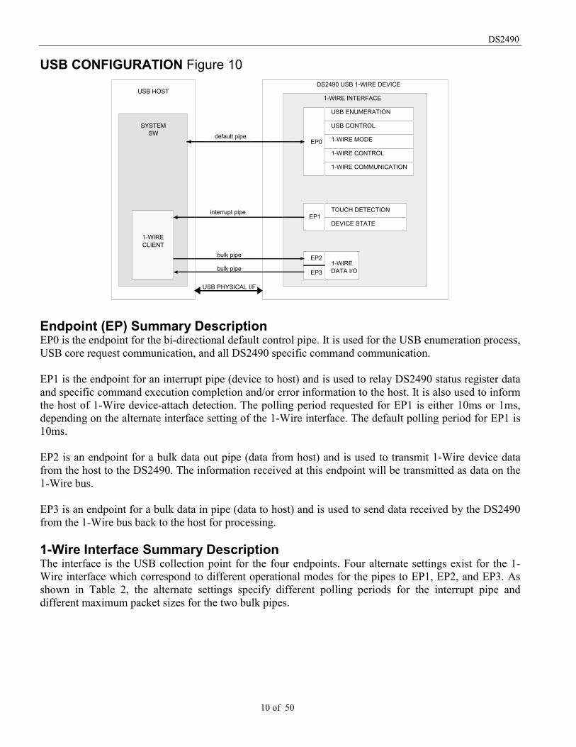
USB COMMUNICATIONCommunication with the DS2490 is performed using USB standard requests, also referred to as corecommands or requests in this document, and DS2490 vendor specific USB commands. All commandcommunication with the DS2490 is performed over the default control pipe. Non-commandcommunication, including 1-Wire device data I/O and DS2490 status information, occurs in a vendor-specific fashion over bulk and interrupt pipes. Configuration of the DS2490 USB controller is shown inFigure 10. As shown, a Dallas Semiconductor vendor-specific 1-Wire device exists with a single 1-Wireinterface. The USB vendor-specific 1-Wire function of the DS2490 will be implemented and controlledby the device driver at the device level of the device class hierarchy, i.e, vendor-specific commands, willbe directed to the device level. Within the 1-Wire interface, four endpoints exist to control andcommunicate with the device. Four alternate settings of the 1-Wire interface exist that correspond todifferent operating modes for the endpoints. Endpoint and interface descriptions are summarized in thefollowing paragraphs.
The DS2490 provides USB remote wake-up capability. Per the USB specification, if a device supportsremote wake-up, it must also provide the ability to enable or disable the remote wake-up function. Inaddition, the remote wake-up feature must be disabled as the power up default or device reset state. Whenthe remote wake-up feature is enabled, the DS2490 will send USB resume signaling to a suspended hostsystem upon detecting a 1-Wire device attachment. It then becomes the responsibility of host systemsoftware to resume operation and to determine what servicing is required for the 1-Wire device.
DS2490
10 of 50
USB CONFIGURATION Figure 10
1-WIRECLIENT
USB HOST
SYSTEMSW
DS2490 USB 1-WIRE DEVICE
1-WIRE INTERFACE
TOUCH DETECTION
DEVICE STATE
1-WIREDATA I/O
EP2
EP3
EP1
USB ENUMERATION
USB CONTROL
1-WIRE CONTROL
EP0default pipe
interrupt pipe
bulk pipe
bulk pipe
USB PHYSICAL I/F
1-WIRE COMMUNICATION
1-WIRE MODE
Endpoint (EP) Summary DescriptionEP0 is the endpoint for the bi-directional default control pipe. It is used for the USB enumeration process,USB core request communication, and all DS2490 specific command communication.
EP1 is the endpoint for an interrupt pipe (device to host) and is used to relay DS2490 status register dataand specific command execution completion and/or error information to the host. It is also used to informthe host of 1-Wire device-attach detection. The polling period requested for EP1 is either 10ms or 1ms,depending on the alternate interface setting of the 1-Wire interface. The default polling period for EP1 is10ms.
EP2 is an endpoint for a bulk data out pipe (data from host) and is used to transmit 1-Wire device datafrom the host to the DS2490. The information received at this endpoint will be transmitted as data on the1-Wire bus.
EP3 is an endpoint for a bulk data in pipe (data to host) and is used to send data received by the DS2490from the 1-Wire bus back to the host for processing.
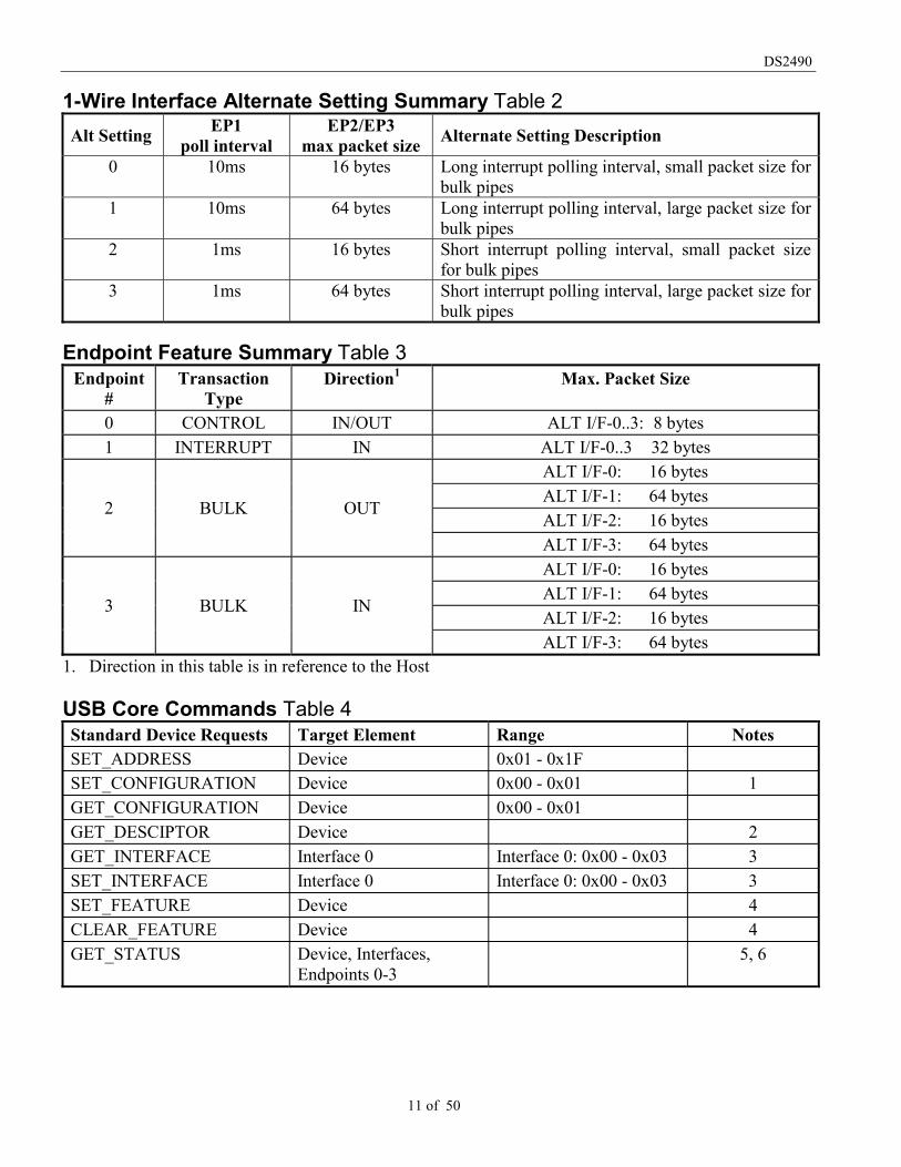
1-Wire Interface Summary DescriptionThe interface is the USB collection point for the four endpoints. Four alternate settings exist for the 1-Wire interface which correspond to different operational modes for the pipes to EP1, EP2, and EP3. Asshown in Table 2, the alternate settings specify different polling periods for the interrupt pipe anddifferent maximum packet sizes for the two bulk pipes.
DS2490
11 of 50
1-Wire Interface Alternate Setting Summary Table 2Alt Setting EP1
poll intervalEP2/EP3
max packet size Alternate Setting Description
0 10ms 16 bytes Long interrupt polling interval, small packet size forbulk pipes
1 10ms 64 bytes Long interrupt polling interval, large packet size forbulk pipes
2 1ms 16 bytes Short interrupt polling interval, small packet sizefor bulk pipes
3 1ms 64 bytes Short interrupt polling interval, large packet size forbulk pipes
Endpoint Feature Summary Table 3Endpoint
#Transaction
TypeDirection1 Max. Packet Size
0 CONTROL IN/OUT ALT I/F-0..3: 8 bytes1 INTERRUPT IN ALT I/F-0..3 32 bytes
ALT I/F-0: 16 bytesALT I/F-1: 64 bytesALT I/F-2: 16 bytes
2 BULK OUT
ALT I/F-3: 64 bytesALT I/F-0: 16 bytesALT I/F-1: 64 bytesALT I/F-2: 16 bytes
3 BULK IN
ALT I/F-3: 64 bytes1. Direction in this table is in reference to the Host
USB Core Commands Table 4Standard Device Requests Target Element Range NotesSET_ADDRESS Device 0x01 - 0x1FSET_CONFIGURATION Device 0x00 - 0x01 1GET_CONFIGURATION Device 0x00 - 0x01GET_DESCIPTOR Device 2GET_INTERFACE Interface 0 Interface 0: 0x00 - 0x03 3SET_INTERFACE Interface 0 Interface 0: 0x00 - 0x03 3SET_FEATURE Device 4CLEAR_FEATURE Device 4GET_STATUS Device, Interfaces,
Endpoints 0-35, 6

DS2490
12 of 50
Notes:1. The only valid configuration values are 0 and 1 for the SET_CONFIGURATION request.
Configuration value 0 corresponds to the non-configured state.2. Only the DEVICE and CONFIGURATION descriptor types are supported for the
GET_DESCRIPTOR request.3. Interface 0 is the only valid interface value for the DS2490.4. The only valid feature selector for the command is DEVICE_REMOTE_WAKE-UP.5. The DS2490 is intended, at a minimum, to be partially bus powered. Remote wake-up can be enabled
or disabled. GET_STATUS requests to the device will return a logic 0 for the self-powered bit fieldand the current state value for the remote wake-up bit.
6. There is no USB core level status information defined for interfaces in USB Specification v1.1. TheDS2490 will always return 0 value data for GET_STATUS requests to interfaces.
DS2490 Vendor-Specific USB CommandsThree different vendor-specific command types exist to control and communicate with the DS2490:Control, Communication, and Mode. Control commands are used to manage various device functionsincluding the processing of communication commands, buffer clearing, and SW reset. Communicationcommands are used for 1-Wire data and command I/O. Mode commands are used to establish the 1-Wireoperational characteristics of the DS2490 such as slew rate, low time, strong pullup, etc. Control,Communication and Mode commands, like USB core requests, are communicated over the default controlpipe at EP0. With one exception as noted below, each command and any associated parameter data areindividually formatted into the 8-byte control transfer setup packet as follows:
bmRequestType bRequest wValue wIndex wLengthRequest type bit map
(1 byte)Command Type
(1 byte)Command(2 bytes)
See Note 1
Command Parameters(2 bytes)
(2 bytes)See Note 2
Notes:1. The one exception to wValue formatting is for the READ STRAIGHT Communication command.
This command requires three parameter bytes that exceed the 2-byte parameter encoding spaceavailable in the wIndex field. For this command only, the wValue field will be formatted as 1command byte and 1 parameter byte. See the command description in Appendix 2 for details.
2. The wLength field is used by the GET COMM CMDS Control command to specify the number ofcommand/parameter bytes to retrieve from the DS2490 command FIFO; see the command descriptionfor specifics. In all other cases the wLength field is not used and must be set to 0x0000.
The bit-mapped bmRequestType field identifies the characteristics of the USB command per Chapter 9of the USB Specification. Fields included in this command describe the direction of the transfer, type ofrequest (core, class, or vendor specific) and the target of the command recipient (device, interface, orendpoint). The only variation on the bmRequestType field for the different DS2490 vendor-specificcommand will be for the transfer direction: host to device, or device to host; the recipient for allcommands will be the device.
The bRequest field contains a 1-byte constant identifying which of the three supported DS2490command types is being sent. The command constants are defined in Appendix 4 and are summarized asfollows:

DS2490
13 of 50
Command Type DescriptionCONTROL_CMD 1-Wire interface control commandsCOMM_CMD 1-Wire interface communication commandsMODE_CMD 1-Wire interface operational mode commands
The 2-byte wValue field is encoded with the specific command. For Control and Mode commands, thefield value corresponds to a specific command constant as defined in Appendix 4. For Communicationcommands, the field has additional embedded command parameters as indicated in Appendix 2. Theexception is the READ STRAIGHT command as described previously.
The 2-byte wIndex is used to hold additional command parameter data when required by the specificcommand.
The wLength field is used in the control transfer setup packet to specify the number of bytes to be sentduring the data stage of a control transfer. The “GET COMM CMDS” control command is the onlyDS2490 command that uses the data stage of the control transfer. Typically, all command data isembedded in the setup stage. Except for the GET COMM CMDS, this field must be set to 0x0000.
DS2490 Control, Communication, and Mode vendor-specific command descriptions and formatting aredefined in Appendices 1, 2, and 3. Vendor-specific commands not defined in the appendices are notsupported by the DS2490 and the device will respond with a STALL if an unsupported command isreceived.
MODE COMMANDSDS2490 1-Wire characteristics and features (speed, durations, slew rate, etc.) are controlled with discreteMode commands and/or embedded Communication command parameters. Parameter values andenable/disable settings are used for characteristic control. Mode settings are stored in the DS2490 StateRegisters and can be read at any time or at the polling interval of EP1. See the section “DEVICEFEEDBACK” for State Register details.
Enable/disable settings are used to control three global features:� Strong pullup to +5V� +12V EPROM programming pulse� Dynamic 1-Wire bus communication speed change through a communication command
The settings for these three global controls are accessible only through Mode commands; the features areeither enabled or disabled with the appropriate Mode command. Specific Communication commandsexist to issue a strong pullup, a programming pulse, or speed change. When the corresponding setting isenabled the feature is usable as part of a communication command when disabled the feature is notusable.
Parameter values and codes are used to specify and control 1-Wire bus characteristics:� 1-Wire bus communication speed� +5V strong pullup duration� +12V programming pulse duration� Pulldown slew rate� Write-1 low time� Data sample offset/Write-0 Recovery time

DS2490
14 of 50
These six settings are controllable with discrete Mode commands or as embedded command/parametervalues in Communications commands.
As listed in Table 5 and summarized previously, there are eight Mode commands. The USB controltransfer setup packet coding to transmit these commands is detailed in Appendix 3. Mode commands areimmediately processed by the DS2490 when they are received. The DS2490 power-on default values forthese parameters are as listed in Table 12. Each command and parameter control is detailed in thefollowing paragraphs.
Mode Command Set Summary Table 5Command FunctionENABLE PULSE Enable/disable 1-Wire strong pullup pulse to 5V and/or +12V programming
pulse.ENABLE SPEEDCHANGE
Enable/disable dynamic change of the 1-Wire speed through acommunication command.
1-WIRE SPEED Communication speed of the 1-Wire bus.STRONG PULLUPDURATION
Duration of 1-Wire strong pullup.
PULLDOWN SLEWRATE
Slew rate of 1-Wire pulldown.
PROG PULSEDURATION
Duration of 1-Wire VPP EPROM programming pulse.
WRITE-1 LOW TIME Duration of 1-Wire Write-1 low time.DSOW0 RECOVERYTIME
Recovery time for the 1-Wire data sample offset / Write-0 transaction.
Mode Command Set Descriptions:
ENABLE PULSE—This command is used to enable or disable a 1-Wire strong pullup pulse to 5Vand/or +12V EPROM programming pulse. Two bit positions in the parameter byte are used to control theenabled/disabled state for each pulse type. The specific pulse is enabled when the respective bit is set to a1 and disabled when set to a 0. The DS2490 power-up default state for both strong pullup andprogramming pulse is disabled.
ENABLE SPEED CHANGE—This command is used to enable or disable a 1-Wire communicationspeed change. Enabled when a TRUE parameter value is passed with the command, disabled with aFALSE. The DS2490 power-up default state for speed change is disabled.
1-WIRE SPEED—This command is used to set the speed of 1-Wire communication; three settings arepossible. The parameter codes to select the desired or required speed are as listed in Table 6. As shown,speed codes 0x3..0xF are undefined. The DS2490 decodes the 3 LSBs of the 1-Wire speed code. Sendinga code other than the defined values in Table 6 will result in undefined behavior. The DS2490 power-updefault communication speed is regular.
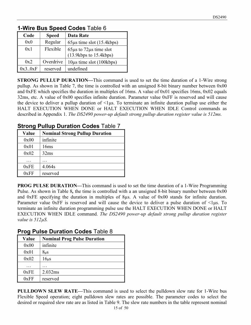
DS2490
15 of 50
1-Wire Bus Speed Codes Table 6Code Speed Data Rate0x0 Regular 65�s time slot (15.4kbps)0x1 Flexible 65�s to 72�s time slot
(13.9kbps to 15.4kbps)0x2 Overdrive 10�s time slot (100kbps)
0x3..0xF reserved undefined
STRONG PULLUP DURATION—This command is used to set the time duration of a 1-Wire strongpullup. As shown in Table 7, the time is controlled with an unsigned 8-bit binary number between 0x00and 0xFE which specifies the duration in multiples of 16ms. A value of 0x01 specifies 16ms, 0x02 equals32ms, etc. A value of 0x00 specifies infinite duration. Parameter value 0xFF is reserved and will causethe device to deliver a pullup duration of <1µs. To terminate an infinite duration pullup use either theHALT EXECUTION WHEN DONE or HALT EXECUTION WHEN IDLE Control commands asdescribed in Appendix 1. The DS2490 power-up default strong pullup duration register value is 512ms.
Strong Pullup Duration Codes Table 7Value Nominal Strong Pullup Duration0x00 infinite0x01 16ms0x02 32ms… …
0xFE 4.064s0xFF reserved
PROG PULSE DURATION—This command is used to set the time duration of a 1-Wire ProgrammingPulse. As shown in Table 8, the time is controlled with a an unsigned 8-bit binary number between 0x00and 0xFE specifying the duration in multiples of 8µs. A value of 0x00 stands for infinite duration.Parameter value 0xFF is reserved and will cause the device to deliver a pulse duration of <1µs. Toterminate an infinite duration programming pulse use the HALT EXECUTION WHEN DONE or HALTEXECUTION WHEN IDLE command. The DS2490 power-up default strong pullup duration registervalue is 512µS.
Prog Pulse Duration Codes Table 8Value Nominal Prog Pulse Duration0x00 infinite0x01 8µs0x02 16µs… …
0xFE 2.032ms0xFF reserved
PULLDOWN SLEW RATE—This command is used to select the pulldown slew rate for 1-Wire busFlexible Speed operation; eight pulldown slew rates are possible. The parameter codes to select thedesired or required slew rate are as listed in Table 9. The slew rate numbers in the table represent nominal
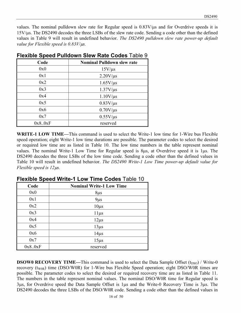
DS2490
16 of 50
values. The nominal pulldown slew rate for Regular speed is 0.83V/�s and for Overdrive speeds it is15V/�s. The DS2490 decodes the three LSBs of the slew rate code. Sending a code other than the definedvalues in Table 9 will result in undefined behavior. The DS2490 pulldown slew rate power-up defaultvalue for Flexible speed is 0.83V/�s.
Flexible Speed Pulldown Slew Rate Codes Table 9Code Nominal Pulldown slew rate0x0 15V/�s0x1 2.20V/�s0x2 1.65V/�s0x3 1.37V/�s0x4 1.10V/�s0x5 0.83V/�s0x6 0.70V/�s0x7 0.55V/�s
0x8..0xF reserved
WRITE-1 LOW TIME—This command is used to select the Write-1 low time for 1-Wire bus Flexiblespeed operation; eight Write-1 low time durations are possible. The parameter codes to select the desiredor required low time are as listed in Table 10. The low time numbers in the table represent nominalvalues. The nominal Write-1 Low Time for Regular speed is 8�s, at Overdrive speed it is 1�s. TheDS2490 decodes the three LSBs of the low time code. Sending a code other than the defined values inTable 10 will result in undefined behavior. The DS2490 Write-1 Low Time power-up default value forFlexible speed is 12�s.
Flexible Speed Write-1 Low Time Codes Table 10Code Nominal Write-1 Low Time0x0 8�s0x1 9�s0x2 10�s0x3 11�s0x4 12�s0x5 13�s0x6 14�s0x7 15�s
0x8..0xF reserved
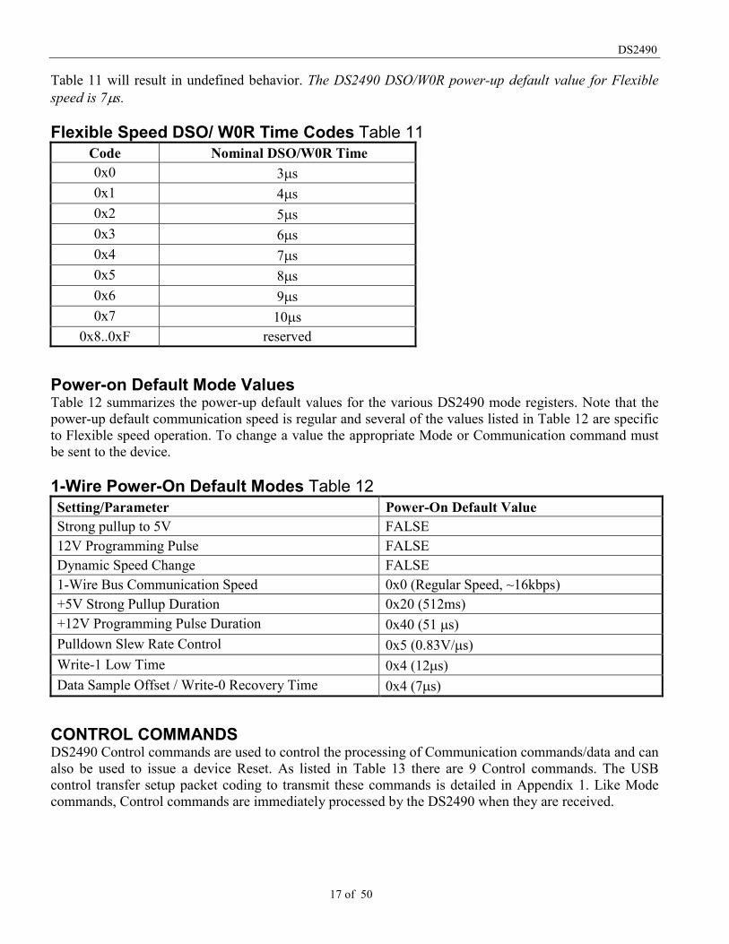
DSOW0 RECOVERY TIME—This command is used to select the Data Sample Offset (tDSO) / Write-0recovery (tW0R) time (DSO/W0R) for 1-Wire bus Flexible Speed operation; eight DSO/W0R times arepossible. The parameter codes to select the desired or required recovery time are as listed in Table 11.The numbers in the table represent nominal values. The nominal DSO/W0R time for Regular speed is3�s, for Overdrive speed the Data Sample Offset is 1�s and the Write-0 Recovery Time is 3�s. TheDS2490 decodes the three LSBs of the DSO/W0R code. Sending a code other than the defined values in
DS2490
17 of 50
Table 11 will result in undefined behavior. The DS2490 DSO/W0R power-up default value for Flexiblespeed is 7�s.
Flexible Speed DSO/ W0R Time Codes Table 11Code Nominal DSO/W0R Time0x0 3�s0x1 4�s0x2 5�s0x3 6�s0x4 7�s0x5 8�s0x6 9�s0x7 10�s
0x8..0xF reserved
Power-on Default Mode ValuesTable 12 summarizes the power-up default values for the various DS2490 mode registers. Note that thepower-up default communication speed is regular and several of the values listed in Table 12 are specificto Flexible speed operation. To change a value the appropriate Mode or Communication command mustbe sent to the device.
1-Wire Power-On Default Modes Table 12Setting/Parameter Power-On Default ValueStrong pullup to 5V FALSE12V Programming Pulse FALSEDynamic Speed Change FALSE1-Wire Bus Communication Speed 0x0 (Regular Speed, ~16kbps)+5V Strong Pullup Duration 0x20 (512ms)+12V Programming Pulse Duration 0x40 (51 �s)Pulldown Slew Rate Control 0x5 (0.83V/�s)Write-1 Low Time 0x4 (12�s)Data Sample Offset / Write-0 Recovery Time 0x4 (7�s)
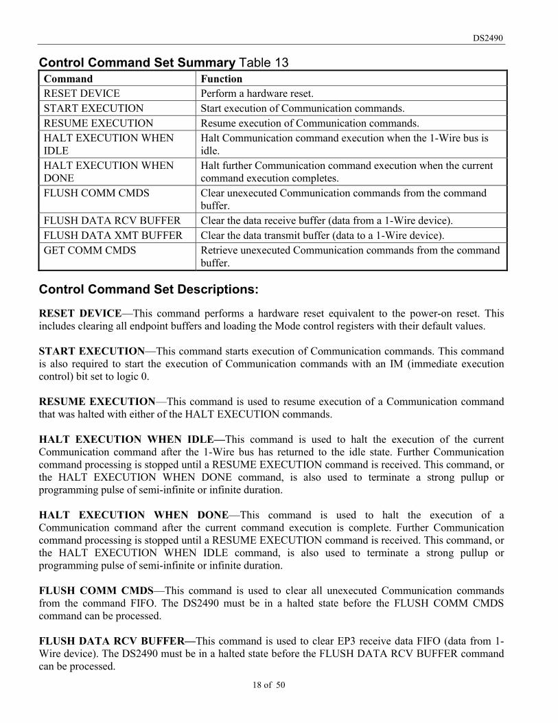
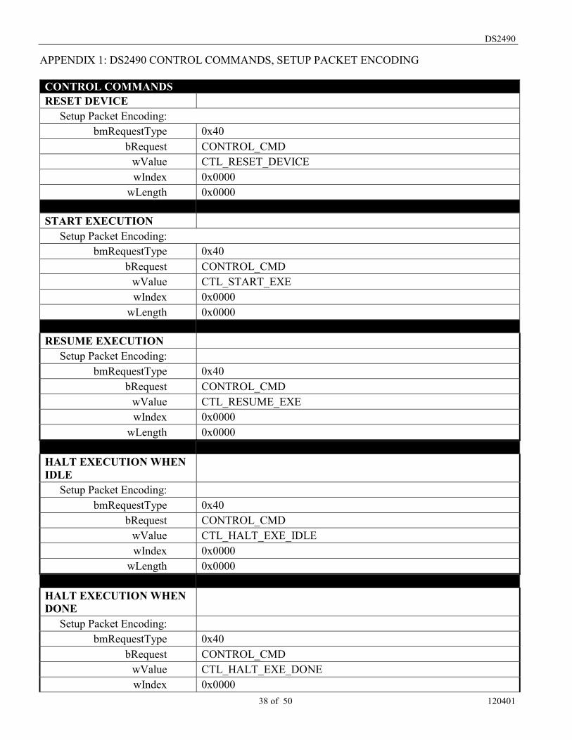
CONTROL COMMANDSDS2490 Control commands are used to control the processing of Communication commands/data and canalso be used to issue a device Reset. As listed in Table 13 there are 9 Control commands. The USBcontrol transfer setup packet coding to transmit these commands is detailed in Appendix 1. Like Modecommands, Control commands are immediately processed by the DS2490 when they are received.
DS2490
18 of 50
Control Command Set Summary Table 13Command FunctionRESET DEVICE Perform a hardware reset.START EXECUTION Start execution of Communication commands.RESUME EXECUTION Resume execution of Communication commands.HALT EXECUTION WHENIDLE
Halt Communication command execution when the 1-Wire bus isidle.
HALT EXECUTION WHENDONE
Halt further Communication command execution when the currentcommand execution completes.
FLUSH COMM CMDS Clear unexecuted Communication commands from the commandbuffer.
FLUSH DATA RCV BUFFER Clear the data receive buffer (data from a 1-Wire device).FLUSH DATA XMT BUFFER Clear the data transmit buffer (data to a 1-Wire device).GET COMM CMDS Retrieve unexecuted Communication commands from the command
buffer.
Control Command Set Descriptions:
RESET DEVICE—This command performs a hardware reset equivalent to the power-on reset. Thisincludes clearing all endpoint buffers and loading the Mode control registers with their default values.
START EXECUTION—This command starts execution of Communication commands. This commandis also required to start the execution of Communication commands with an IM (immediate executioncontrol) bit set to logic 0.
RESUME EXECUTION—This command is used to resume execution of a Communication commandthat was halted with either of the HALT EXECUTION commands.
HALT EXECUTION WHEN IDLE—This command is used to halt the execution of the currentCommunication command after the 1-Wire bus has returned to the idle state. Further Communicationcommand processing is stopped until a RESUME EXECUTION command is received. This command, orthe HALT EXECUTION WHEN DONE command, is also used to terminate a strong pullup orprogramming pulse of semi-infinite or infinite duration.
HALT EXECUTION WHEN DONE—This command is used to halt the execution of aCommunication command after the current command execution is complete. Further Communicationcommand processing is stopped until a RESUME EXECUTION command is received. This command, orthe HALT EXECUTION WHEN IDLE command, is also used to terminate a strong pullup orprogramming pulse of semi-infinite or infinite duration.
FLUSH COMM CMDS—This command is used to clear all unexecuted Communication commandsfrom the command FIFO. The DS2490 must be in a halted state before the FLUSH COMM CMDScommand can be processed.
FLUSH DATA RCV BUFFER—This command is used to clear EP3 receive data FIFO (data from 1-Wire device). The DS2490 must be in a halted state before the FLUSH DATA RCV BUFFER commandcan be processed.

DS2490
19 of 50
FLUSH DATA XMT BUFFER—This command is used to clear EP2 transmit data FIFO (data to 1-Wire device). The DS2490 must be in a halted state before the FLUSH DATA XMT BUFFER commandcan be processed.
GET COMM CMDS—This command is used to retrieve unexecuted Communication commands andparameters from the command FIFO. The DS2490 must be in a halted state before the GET COMMCMDS command can be processed. Unexecuted commands are returned over EP0 in the control transferdata phase. Host software is responsible for determining the number of command/parameter bytes to bereturned and specifying the value in the wLength field of the control transfer setup packet.Commands/parameters are deleted from the FIFO as they are transmitted to the host; the commandpointer used with the FIFO is updated as values are read. Any commands/parameters that are nottransferred remain in the FIFO and will be processed when command execution resumes. If the wLengthvalue passed is larger than the number of command/parameter bytes, the DS2490 will terminate thecontrol transfer with a short data packet.
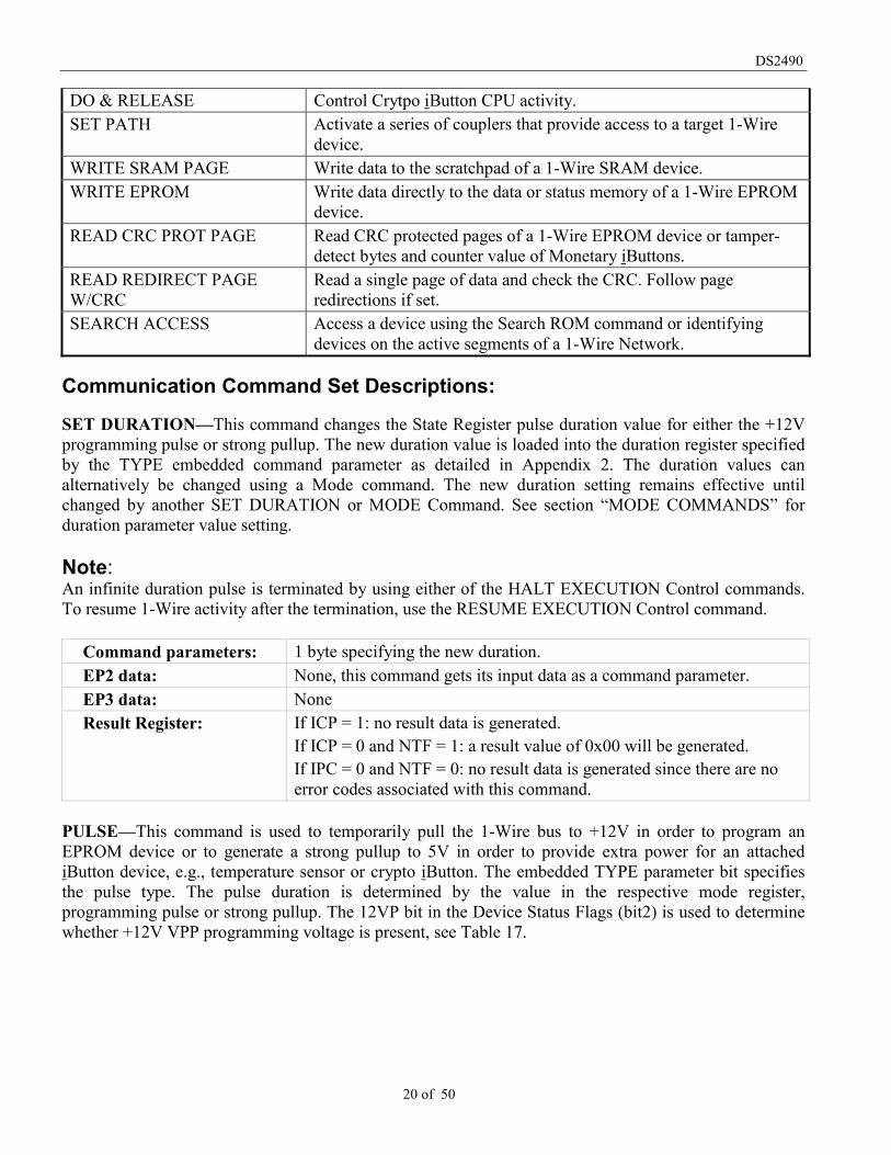
COMMUNICATION COMMANDSCommunication commands are used to communicate with and control an attached 1-Wire device(s).There are 15 Communication commands as summarized in Table 14. Communication commands alsocontain embedded command bits for conditional control or additional functionality. Appendix 2 detailsthe embedded command bit purpose/formatting as well as the control transfer setup packet coding totransmit the command/parameter data to the DS2490.
Unlike Mode and Control commands, Communication command processing is controlled by hostsoftware by setting embedded command bits within a Communication command. For example, acommand macro form is supported in which several Communication commands and parameter data aresent/buffered in the DS2490 and then processed as a group. Embedded command bit ICP is used to createmacro command sets. Also, unlike Mode and Control commands, several forms of Communicationcommand monitoring exist for host software to track processing progress.
Depending on the settings of embedded communication command bits ICP and NTF, see APPENDIX 2,a Result Register value may be generated to provide command processing feedback. Communicationcommand buffer (FIFO) status and 1-Wire data transmit/received buffers (EP2/3 FIFOs) status can alsobe monitored via the State Registers. See the section “DEVICE FEEDBACK” for details on commandmonitoring.
Communication Command Set Summary Table 14COMMAND FUNCTIONSET DURATION Change duration of strong pullup or programming pulse.PULSE Perform strong pullup or generate programming pulse.1-WIRE RESET Generate 1-Wire reset pulse.BIT I/O 1-Wire single data bit I/O.BYTE I/O 1-Wire data byte I/O.BLOCK I/O 1-Wire data block I/O.MATCH ACCESS Address a device on the 1-Wire bus.READ STRAIGHT Transmit a data preamble and read back data.
DS2490
20 of 50
DO & RELEASE Control Crytpo iButton CPU activity.SET PATH Activate a series of couplers that provide access to a target 1-Wire
device.WRITE SRAM PAGE Write data to the scratchpad of a 1-Wire SRAM device.WRITE EPROM Write data directly to the data or status memory of a 1-Wire EPROM
device.READ CRC PROT PAGE Read CRC protected pages of a 1-Wire EPROM device or tamper-
detect bytes and counter value of Monetary iButtons.READ REDIRECT PAGEW/CRC
Read a single page of data and check the CRC. Follow pageredirections if set.
SEARCH ACCESS Access a device using the Search ROM command or identifyingdevices on the active segments of a 1-Wire Network.
Communication Command Set Descriptions:
SET DURATION—This command changes the State Register pulse duration value for either the +12Vprogramming pulse or strong pullup. The new duration value is loaded into the duration register specifiedby the TYPE embedded command parameter as detailed in Appendix 2. The duration values canalternatively be changed using a Mode command. The new duration setting remains effective untilchanged by another SET DURATION or MODE Command. See section “MODE COMMANDS” forduration parameter value setting.
Note:An infinite duration pulse is terminated by using either of the HALT EXECUTION Control commands.To resume 1-Wire activity after the termination, use the RESUME EXECUTION Control command.
Command parameters: 1 byte specifying the new duration.EP2 data: None, this command gets its input data as a command parameter.EP3 data: NoneResult Register: If ICP = 1: no result data is generated.
If ICP = 0 and NTF = 1: a result value of 0x00 will be generated.If IPC = 0 and NTF = 0: no result data is generated since there are noerror codes associated with this command.
PULSE—This command is used to temporarily pull the 1-Wire bus to +12V in order to program anEPROM device or to generate a strong pullup to 5V in order to provide extra power for an attachediButton device, e.g., temperature sensor or crypto iButton. The embedded TYPE parameter bit specifiesthe pulse type. The pulse duration is determined by the value in the respective mode register,programming pulse or strong pullup. The 12VP bit in the Device Status Flags (bit2) is used to determinewhether +12V VPP programming voltage is present, see Table 17.
DS2490
21 of 50
Command parameters: NoneEP2 data: NoneEP3 data: NoneResult Register: Code Condition
VPP ICP = 0, NTF = 0 or 1: no +12V was sensed.0x00 ICP = 0, NTF = 1: no error detectedNone ICP = 0, NTF = 0: no error detectedNone ICP = 1
1-WIRE RESET—This command is used to generate a reset pulse on the 1-Wire bus and to optionallychange the 1-Wire speed. The new speed will take effect only if the embedded command bit SE is set to1. When the 1-WIRE RESET is sent after an Overdrive Skip ROM command, SE must be 1 and the newspeed must be 0x02. See MODE CONTROL section for additional communication speed information. Toswitch back to regular speed, set SE = 1 and the new speed parameter to 0x00 (regular) or 0x01 (flexible).
Command parameters: 1 byte specifying new speed after the reset.EP2 data: NoneEP3 data: NoneResult Register: Code Condition
SH, NRS, APP ICP = 0, NTF = 0 or 1: An abnormal condition oran Alarming Presence Pulse was detected
0x00 ICP = 0, NTF = 1: no error detectedNone ICP = 0, NTF = 0: no error detectedNone ICP = 1
BIT I/O - This command generates a single time slot on the 1-Wire bus and reads back the response.Data bit d3 (D) of command byte 1 specifies the value to be written to the 1-Wire bus. This time slot mayoptionally be followed by a strong pullup using embedded command bits SPU and CIB. With CIB = 1, arequested strong pullup will only occur if the read-back revealed a 0. Data is returned to the host only ifthe embedded command bit ICP = 0. If ICP = 0, the bit read from the 1-Wire device is stored in theEP3 FIFO and is read by the host using an EP3 bulk transaction.
Command parameters: None.EP2 data: None, this command gets its input data as a command parameter.EP3 data: Length Description
If ICP = 0: 1 byte Bit read back from the 1-Wire device.If ICP = 1: None No data is returned.
Result Register: If ICP = 1: no result data is generated.If ICP = 0 and NTF = 1: a result value of 0x00 will be generated.If IPC = 0 and NTF = 0: no result data is generated since there are noerror codes associated with this command.
BIT I/O Read Back Byte Table 15bit7 bit6 bit5 bit4 bit3 bit2 bit1 bit0
0 0 0 0 0 0 0 D
DS2490
22 of 50
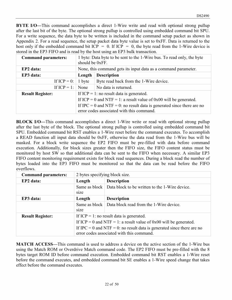
BYTE I/O—This command accomplishes a direct 1-Wire write and read with optional strong pullupafter the last bit of the byte. The optional strong pullup is controlled using embedded command bit SPU.For a write sequence, the data byte to be written is included in the command setup packet as shown inAppendix 2. For a read sequence, the setup packet data byte value is set to 0xFF. Data is returned to thehost only if the embedded command bit ICP = 0. If ICP = 0, the byte read from the 1-Wire device isstored in the EP3 FIFO and is read by the host using an EP3 bulk transaction.
Command parameters: 1 byte: Data byte to be sent to the 1-Wire bus. To read only, the byteshould be 0xFF.
EP2 data: None, this command gets its input data as a command parameter.EP3 data: Length Description
If ICP = 0: 1 byte Byte read back from the 1-Wire device.If ICP = 1: None No data is returned.
Result Register: If ICP = 1: no result data is generated.If ICP = 0 and NTF = 1: a result value of 0x00 will be generated.If IPC = 0 and NTF = 0: no result data is generated since there are noerror codes associated with this command.
BLOCK I/O—This command accomplishes a direct 1-Wire write or read with optional strong pullupafter the last byte of the block. The optional strong pullup is controlled using embedded command bitSPU. Embedded command bit RST enables a 1-Wire reset before the command executes. To accomplisha READ function all input data should be 0xFF, otherwise the data read from the 1-Wire bus will bemasked. For a block write sequence the EP2 FIFO must be pre-filled with data before commandexecution. Additionally, for block sizes greater then the FIFO size, the FIFO content status must bemonitored by host SW so that additional data can be sent to the FIFO when necessary. A similar EP3FIFO content monitoring requirement exists for block read sequences. During a block read the number ofbytes loaded into the EP3 FIFO must be monitored so that the data can be read before the FIFOoverflows.
Command parameters: 2 bytes specifying block size.EP2 data: Length Description
Same as blocksize
Data block to be written to the 1-Wire device.
EP3 data: Length DescriptionSame as blocksize
Data block read from the 1-Wire device.
Result Register: If ICP = 1: no result data is generated.If ICP = 0 and NTF = 1: a result value of 0x00 will be generated.If IPC = 0 and NTF = 0: no result data is generated since there are noerror codes associated with this command.
MATCH ACCESS—This command is used to address a device on the active section of the 1-Wire bususing the Match ROM or Overdrive Match command code. The EP2 FIFO must be pre-filled with the 8bytes target ROM ID before command execution. Embedded command bit RST enables a 1-Wire resetbefore the command executes, and embedded command bit SE enables a 1-Wire speed change that takeseffect before the command executes.

DS2490
23 of 50
Command parameters: 2 bytes: match command byte, new 1-Wire speed byte (optional).EP2 data: Length Description
8 bytes ROM ID of the device to be accessed.EP3 data: NoneResult Register: If ICP = 1: no result data is generated.
If ICP = 0 and NTF = 1: a result value of 0x00 will be generated.If IPC = 0 and NTF = 0: no result data is generated since there are noerror codes associated with this command.
READ STRAIGHT—This command transmits a user-specified preamble of data to the 1-Wire bus andthen reads back as many bytes as specified. The preamble typically consists of a 1-Wire command codefollowed by TA1 and TA2. It is possible to include a Match ROM command and ROM ID in thepreamble to also address a device at the current speed. This command can also be used to copy thescratchpad or disconnect a path. Embedded command bit RST enables a 1-Wire reset before thecommand executes. The EP2 FIFO must be pre-filled with preamble data before command execution.Additionally, for preamble sizes greater then the FIFO size, the FIFO content status must be monitored byhost SW so that additional data can be sent to the FIFO when necessary. A similar EP3 FIFO contentmonitoring requirement exists for the block read. During a block read, the number of bytes loaded intothe EP3 FIFO must be monitored so that the data can be read before the FIFO overflows.
Command parameters: 3 bytes: 2-byte parameter specifying block read size, byte specifyingpreamble size.
EP2 data: Length DescriptionSame aspreamble size
Preamble data to be written to the 1-Wire device.
EP3 data: Length DescriptionSame as blocksize
Data block read from the 1-Wire device.
Result Register: If ICP = 1: no result data is generated.If ICP = 0 and NTF = 1: a result value of 0x00 will be generated.If IPC = 0 and NTF = 0: no result data is generated since there are noerror codes associated with this command.
DO & RELEASE—This command is typically used to control the activity of the CPU of the cryptoiButton, which requires a release sequence. This command can also be used to read from or write to theI/O buffer or Status Register of the crypto iButton. A short preamble (3 bytes) consists of a 1-Wirecommand code followed by the release sequence. A four-byte preamble with embedded command bit R= 1 consists of a 1-Wire command code followed by length byte and the release sequence. A 4-bytepreamble with embedded command bit R = 0 consists of a 1-Wire command code followed by a statusbyte and the release sequence. The long preamble (minimum 5 bytes, embedded command bit R = 0)consists of a 1-Wire command, a length byte, data bytes and the release sequence. In this case, the lengthbyte indicates the total number of bytes between the length byte and release sequence. The leastsignificant byte of the release sequence is transmitted first. Embedded command bit SPU must be 1 whentrying to run (start, continue) the CPU of the crypto iButton. In all other cases, SPU should be 0.Additionally, embedded command bit F can be used to clear the communication command buffer andEP2/3 FIFOs if an error occurs during execution of the command. The EP2 FIFO must be pre-filled withpreamble data before command execution. Additionally, for preamble sizes greater then the FIFO size,

DS2490
24 of 50
the FIFO content status must be monitored by host SW so that additional data can be sent to the FIFOwhen necessary.
A similar EP3 FIFO content monitoring requirement exists for the block read. During a block read thenumber of bytes loaded into the EP3 FIFO must be monitored so that the data can be read before theFIFO overflows.
Command parameters: 1 byte specifying preamble size.EP2 data: Length Description
Same aspreamble size
Preamble data to be written to the 1-Wire device.
EP3 data: Length DescriptionIf R = 1 and preamble
size � 4:As specified inthe second byteof thepreamble
Data read from the 1-Wire device.
If R = 0: None No data is returned (this is a write application).Result Register: Code Condition
CRC, CMP ICP = 0, NTF = 0 or 1: Bad CRC or the releasesequence was not accepted.
0x00 ICP = 0, NTF = 1: no error detectedNone ICP = 0, NTF = 0: no error detectedNone ICP = 1
SET PATH—This command is used to activate a series of couplers that finally provide the access to thetarget 1-Wire device. Embedded command bit RST enables a 1-Wire reset before the command executes.Additionally, embedded command bit F can be used to clear the communication command buffer andEP2/3 FIFOs if an error occurs during execution of the command. The EP2 FIFO must be pre-filled withcoupler data before command execution. Additionally, for coupler data sizes greater then the EP2 FIFOsize, the FIFO content status must be monitored by host SW so that additional data can be sent to theFIFO when necessary. Upon completion of command execution, the EP3 FIFO is loaded with a 1-bytevalue that indicates the number of couplers activated. An NRS error code is an indication that there wasno presence pulse on the branch that was to be connected.
Command parameters: 1 byte specifying number of couplers that need to be activated to set-upthe path to the target device.
EP2 data: Length Description9 bytes perlevel
8 bytes ROM ID of the coupler to be activatedfollowed by the Smart-On command code for eitherthe main or auxiliary 1-Wire coupler output.
EP3 data: Length Description1 byte Number of couplers successfully activated; should be
the same as the number of levels.Result Register: Code Condition
CMP, SH,NRS
ICP = 0, NTF = 0 or 1: An error condition is detected.
0x00 ICP = 0, NTF = 1: no error detected
DS2490
25 of 50
None ICP = 0, NTF = 0: no error detectedNone ICP = 1
WRITE SRAM PAGE—This command is used to write data to the scratchpad of an SRAM device andoptionally check the CRC. To copy the data to its final memory location, it is required to send the READSTRAIGHT command with a “copy scratchpad” preamble and a 0 block size. Embedded command bitDT = 1 activates the CRC16 generator. This command is also applicable to the Write IPR function of theCrypto iButton if embedded command bit CIB = 1. To write a partial page the page size parameter andthe target address need to be set accordingly. The EP2 FIFO must be pre-filled with preamble and SRAMdata before command execution. Additionally, for data page sizes greater then the EP2 FIFO size, theFIFO content status must be monitored by host SW so that additional data can be sent to the FIFO whennecessary.
Command parameters: 1 byte specifying page size. This specifies the number of bytes to besent to the 1-Wire device following a 2- or 3-byte preamble. Thisnumber is typically identical to the page size; a value of 0x00 indicates a256-byte page.
EP2 data: Length DescriptionIf CIB = 0: 3-bytes + page
sizePreamble and data bytes to be sent to the 1-WireSRAM device. 3-byte preamble: 1-Wire commandcode, TA1, TA2 (typical).
If CIB = 1: 2-bytes + pagesize
Preamble and data bytes to be sent to the 1-WireSRAM device. 2-byte preamble: 1-Wire commandcode, length information.
EP3 data: NoneResult Register: Code Condition
CRC ICP = 0, NTF = 0 or 1: and an error condition (only ifDT = 1).
0x00 ICP = 0, NTF = 1: no error detectedNone ICP = 0, NTF = 0: no error detectedNone ICP = 1
DS2490
26 of 50
WRITE EPROM—This command is used to write data directly to the data or status memory of a 1-WireEPROM device. If embedded command bit DT = 1, the CRC16 generator is selected; if DT = 0, CRC8 isused. Embedded command bit Z controls the method used for comparison of the data written to the 1-Wire device. Additionally, embedded command bit F can be used to clear the Communication commandbuffer and EP2/3 FIFOs if an error occurs during execution of the command. The EP2 FIFO must be pre-filled with preamble and EPROM data before command execution. Additionally, for data block sizesgreater then the EP2 FIFO size, the FIFO content status must be monitored by host SW so that additionaldata can be sent to the FIFO when necessary.
Command parameters: 2 bytes specifying block size.EP2 data: Length
3-bytes +block size
Preamble and data bytes to be sent to the 1-WireEPROM device. 3-byte preamble: 1-Wire commandcode, TA1, TA2 (typical).
EP3 data: NoneResult Register: Code Condition
CRC, CMP,VPP
ICP = 0, NTF = 0 or 1: and an error condition.
0x00 ICP = 0, NTF = 1: no error detectedNone ICP = 0, NTF = 0: no error detectedNone ICP = 1
READ CRC PROT PAGE—This command is used to read one or multiple CRC-protected pages ofEPROM devices and to read tamper-detect bytes and counter value of Monetary iButtons. If embeddedcommand bit DT = 1, the CRC16 generator is selected; if DT = 0, CRC8 is used. Embedded command bitCIB is used to specify either a 2- or 3-byte read preamble. Additionally, embedded command bit F can beused to clear the Communication command buffer and EP2/3 FIFOs if an error occurs during executionof the command. The command can also be used to read a single partial page up to the end of that pageand reading the PIOs of a DS2406. This command is also applicable to the Read IPR function of thecrypto iButton if CIB = 1. The EP2 FIFO must be pre-filled with preamble data before commandexecution. To prevent overflow, the EP3 FIFO must be monitored (and read if necessary) duringcommand execution if reading more data than the size of the EP3 FIFO.

DS2490
27 of 50
Command parameters: 2 bytes: 1 byte page size, 1 byte number of pages. Note that the PageSize byte parameter value must be of the form log2(actual page size).For example, if the actual page size is 3210, then the Page Sizeparameter would need to be 0x05. Typical page sizes are 32 decimal fordata memory and 8 for status memory. A page size of 0x00 indicates a256-byte page.
EP2 data: LengthIf CIB = 0: 3-bytes 3-byte preamble: 1-Wire command code, TA1, TA2
(typical).If CIB = 1: 2-bytes 2-byte preamble: 1-Wire command code, length
information.EP3 data: Length Description
(page size xnumber ofpages)
Data read from the 1-Wire device.
Result Register: Code ConditionCRC ICP = 0, NTF = 0 or 1: and an error condition.0x00 ICP = 0, NTF = 1: no error detectedNone ICP = 0, NTF = 0: no error detectedNone ICP = 1
READ REDIRECT PAGE W/CRC—This command is used to read a single page of data and check theCRC. If the page is not redirected, the host will receive the page number and all its data. If the page isredirected and embedded command bit CH = 1 the device will follow the trail of redirections until a pageis found that is not redirected. When found, the host will receive the page number and all data of thatparticular page. If CH = 0 and the first read attempt reveals a redirection the host will only receive thenumber of the page the addressed page is redirected to. Reading starts at a page boundary. Additionally,embedded command bit F can be used to clear the communication command buffer and EP2/3 FIFOs ifan error occurs during execution of the command. An NRS error code is an indication of an infinite loop.The EP2 FIFO must be pre-filled with ROM ID and command code data before command execution. Toprevent overflow, the EP3 FIFO must be monitored (and read if necessary) during command execution ifreading more data than the size of the EP3 FIFO.

DS2490
28 of 50
Command parameters: 2 bytes: 1 byte page size, 1 byte page address. Page size byte indicatesthe number of bytes that are considered a page. Typical page sizes are32 decimal for data memory, 8 for status memory, and 40 decimal forMonetary iButtons. A page size of 0x00 indicates a 256-byte page. Thepage address specifies the page number to be used for the first readattempt.
EP2 data: Length9 bytes 8 bytes ROM ID of the 1-Wire device to be accessed
followed by the 1-Wire command code for “ExtendedRead Memory”.
EP3 data: Length DescriptionIf CH = 1 or page is not
redirected:1 byte + pagesize
Page number and contents of the page.
If CH = 0 and page isredirected:
1 byte Number of the page the addressed page is redirectedto.
Result Register: Code ConditionRDP, CRC,NRS
ICP = 0, NTF = 0 or 1: and an error condition.
0x00 ICP = 0, NTF = 1: no error detectedNone ICP = 0, NTF = 0: no error detectedNone ICP = 1
SEARCH ACCESS—The SEARCH ACCESS command is used to either access a device using theSearch ROM command or to identify the devices on the active segments of a 1-Wire Network. Embeddedcommand bit SM is used to specify the type of search. Embedded command bit RTS is used to controldiscrepancy information reporting. Additionally, embedded command bit F can be used to clear theCommunication command buffer and EP2/3 FIFOs if an error occurs during execution of the command.An NRS error code indicates that there was no response on at least one of the 64 bits of the ROM search.The EP2 FIFO must be pre-filled with ROM ID data before command execution. To prevent overflow,the EP3 FIFO must be monitored (and read if necessary) during command execution if returning moredata than the size of the EP3 FIFO.
DS2490
29 of 50
Command parameters: 2 bytes: 1 byte 1-Wire command (Search ROM or Conditional SearchROM), 1 byte for number of devices. The number of devices bytespecifies the maximum number of devices to be discovered in a singlecommand call. A value of 0x00 indicates that all devices on the 1-WireNetwork are to be discovered.
EP2 data: Length8 bytes ROM ID of the 1-Wire device to be accessed (SM = 0)
or ROM ID with which to start the search (SM = 1).EP3 data: Length Description
If SM = 0: None No data is returned.If SM = 1: Varies, blocks
of 8 bytes.ROM IDs of the devices discovered followed by 8bytes discrepancy information (if RTS = 1 and thenumbers of devices on the 1-Wire Network is higherthan specified in the second parameter.
Result Register: Code ConditionEOS, NRS ICP = 0, NTF = 0 or 1: and an error condition.0x00 ICP = 0, NTF = 1: no error detectedNone ICP = 0, NTF = 0: no error detectedNone ICP = 1
DS2490
30 of 50
DEVICE FEEDBACKDS2490 state and result feedback are provided to the host over the EP1 interrupt pipe. The host interruptpolling period for EP1 transfers is controlled by the alternate setting of the 1-Wire USB Interface asdescribed in the section: 1-Wire Interface Summary Description. As shown in Table 16, up to 32 bytes offeedback data are returned. As a minimum, 16 bytes of STATE REGISTER data will be delivered at eachpolling interval (or USB IN transaction to EP1); the position and definition of these data values are listedin Table 17. In addition, as shown in Table 18, between 0 and 16 extra bytes of RESULT REGISTERdata will be delivered with feedback data. This consists of communication command processing resultdata as controlled by the embedded communication command bits ICP and NTF and notification bytes for1-Wire device arrival detection. If there are less than 32 bytes of result and state register data to return,the DS2490 will terminate the IN transaction with a short or zero data packet.
Data is loaded into the RESULT REGISTER buffer based on embedded communication command bitsNTF and ICP or upon detection of a 1-Wire device attachment. There is no defined offset position fordata values in this buffer. Knowledge of communication command ordering sent to the DS2490 must bemaintained on the host to properly interpret the returned data values. In addition, a parse of the data isrequired to determine whether or not a 1-Wire detect value is included; the value of the 1-Wire detectbyte is unique. Table 19 defines the 1-Wire detect byte and data values that result from Communicationcommand processing.
Interrupt Transfer Data Summary Table 16OFFSET DATA
0x00 to 0x0F STATE REGISTERS0x10 to 0x1F1 RESULT REGISTERS
Notes:1. The number of RESULT RESIGTER values will vary depending on the setting of embedded
communication command bits NTF and ICP, the number of communication commands processedsince the previous EP1 polling period, or whether a 1-Wire device was detected.
DS2490 STATE REGISTERS Table 17Description Offset DataEnable Flags 0x00 bit7 bit6 bit5 bit4 bit3 bit2 bit1 bit0
-- -- -- -- -- SPCE PRGE SPUESPUE If set to 1, the strong pullup to 5V is enabled, if set to 0,
it is disabled.PRGE If set to 1, a 12V programming pulse is enabled, if set to
0, it is disabled.SPCE If set to 1, a dynamic 1-Wire bus speed change through a
Communication command is enabled, if set to 0, it isdisabled.
bit 3..7 These bits are reserved.1-Wire Speed 0x01 current 1-Wire bus speed codeStrong Pullup Duration 0x02 current pullup durationProgramming Pulse 0x03 current programming pulse duration

DS2490
31 of 50
Description Offset DataDurationPulldown Slew RateControl
0x04 current pulldown slew rate code
Write-1 Low Time 0x05 current Write-1 low time codeData Sample Offset /Write-0 Recovery Time
0x06 current data sample offset/ Write-0 recovery time code
Reserved (Test Register) 0x07Device Status Flags 0x08 bit7 bit6 bit5 bit4 bit3 bit2 bit1 bit0
EP0F -- IDLE HALT PMOD 12VP PRGA SPUABit Definitions:
SPUA if set to 1, the strong pullup to 5V is currently active, ifset to 0, it is inactive.
PRGA if set to 1, a 12V programming pulse is currently beinggenerated, if set to 0, it is not.
12VP if set to 1, the external 12V programming voltage ispresent, if set to 0, it is not present.
PMOD if set to 1, the DS2490 is powered from USB andexternal sources, if set to 0, all DS2490 power isprovided from USB.
HALT if set to 1, the DS2490 is currently halted, if set to 0, thedevice is not halted.
IDLE if set to 1, the DS2490 is currently idle, if set to 0, thedevice is not idle.
bit 6: ReservedEPOF: Endpoint 0 FIFO status, see Note 1.
CommunicationCommand, Byte 1
0x09 Communication command currently being processed. If the deviceis idle, a register value of 0x00 is sent.
CommunicationCommand, Byte 2
0x0A Communication command currently being processed. If the deviceis idle, a register value of 0x00 is sent.
CommunicationCommand Buffer Status
0x0B Number of data bytes currently contained in the 16-byte FIFO usedto hold communication commands.
1-Wire Data Out BufferStatus
0x0C Number of data bytes currently contained in the 128-byte FIFOused to write data to the 1-Wire bus.
1-Wire Data In BufferStatus
0x0D Number of data bytes currently contained in the 128-byte commandFIFO used to read data from the 1-Wire bus.
Reserved (Test Register) 0x0E ReservedReserved (Test Register) 0x0F Reserved
Notes:1. If EP0F is set to 1, the Endpoint 0 FIFO was full when a new control transfer setup packet was
received. This is an error condition in that the setup packet received is discarded due to the full

DS2490
32 of 50
condition. To recover from this state the USB host must send a CTL_RESET_DEVICE command; thedevice will also recover with a power on reset cycle. Note that the DS2490 will accept and process aCTL_RESET_DEVICE command if the EP0F = 1 state occurs. If EP0F = 0, no FIFO error conditionexists.
DS2490 RESULT REGISTERS Table 18Offset1,2 Data
0x10 value0x11 value
… …0x1F value
Notes:1. Since Result Registers follow State Registers for interrupt transfers, the register offset starting value
shown in Table 18 for Result Registers follows the last value of Table 17 State Registers.2. The number of RESULT RESIGTER values will vary depending on the setting of embedded
communication command bits NTF and ICP, the number of communication commands processedsince the previous EP1 polling period, or whether a 1-Wire device was detected.
DS2490 RESULT REGISTER VALUE DEFINITION Table 19Data Value Description Data1-Wire Device Detect Byte 0xA5Communication Command ErrorResult
bit7 bit6 bit5 bit4 bit3 bit2 bit1 bit0
EOS RDP CRC CMP VPP APP SH NRS
Bit Definitions:EOS A value of 1 indicates that a SEARCH ACCESS with
SM = 1 ended sooner than expected reporting less ROMID’s than specified in the “number of devices”parameter.
RDP A value of 1 indicates that a READ REDIRECT PAGEWITH/CRC encountered a page that is redirected.
CRC A value of 1 indicates that a CRC error occurred whenexecuting one of the following commands: WRITESRAM PAGE, WRITE EPROM, READ CRC PROTPAGE, or READ REDIRECT PAGE W/CRC.
CMP A value of 1 indicates an error with one of the following:Error when reading the confirmation byte with a SETPATH command. The WRITE EPROM command didnot program successfully. There was a differencebetween the byte written and then read back with aBYTE I/O command
DS2490
33 of 50
Data Value Description DataVPP A value of 1 indicates that during a PULSE with TYPE =
1 or WRITE EPROM command the 12V programmingpulse was not seen on the 1-Wire bus; this could indicatethat there were other devices on the bus that clamped thevoltage to a value lower than VPP or that theprogramming pulse was disabled with a mode command.
APP A value of 1 indicates that a 1-WIRE RESET revealed anAlarming Presence Pulse.
SH A value of 1 indicates that a 1-WIRE RESET revealed ashort to the 1-Wire bus or the SET PATH commandcould not successfully connect a branch due to a short.
NRS A value of 1 indicates an error with one of the following:1-WIRE RESET did not reveal a Presence Pulse. SETPATH command did not get a Presence Pulse from thebranch that was to be connected. No response from oneor more ROM ID bits during a SEARCH ACCESScommand.
A value of 0 in any of these fields indicates that the errorcondition was not detected.
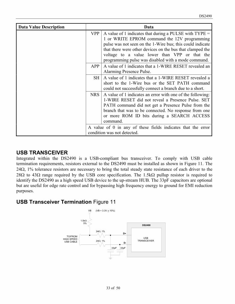
USB TRANSCEIVERIntegrated within the DS2490 is a USB-compliant bus transceiver. To comply with USB cabletermination requirements, resistors external to the DS2490 must be installed as shown in Figure 11. The24�, 1% tolerance resistors are necessary to bring the total steady state resistance of each driver to the28� to 43� range required by the USB core specification. The 1.5k� pullup resistor is required toidentify the DS2490 as a high speed USB device to the up-stream HUB. The 33pF capacitors are optionalbut are useful for edge rate control and for bypassing high frequency energy to ground for EMI reductionpurposes.
USB Transceiver Termination Figure 11
USBTRANSCEIVER
24�, 1%
24�, 1%
DS2490
D+
D-
1.5k�5%
VB (VB = 3.3V + 10%)
TO/FROMHIGH SPEED
USB CABLE
33pF 33pF
DS2490
34 of 50
SUSPEND OUTPUTSuspend output signal ( SUSO ) operation is a function of both the USB device state of the DS2490(configured or unconfigured) and the USB suspend state. A truth table for signal operation is listed inTable 20. This signal could be used stand-alone or combined with other external signals to power downcircuitry external to the DS2490, such as power sources. The SUSO signal is an open drain output andrequires an external pullup.
Suspend Output Operation Table 20Device State Suspend State SUSOunconfigured don’t care HIGHconfigured not suspended HIGHconfigured suspended LOW
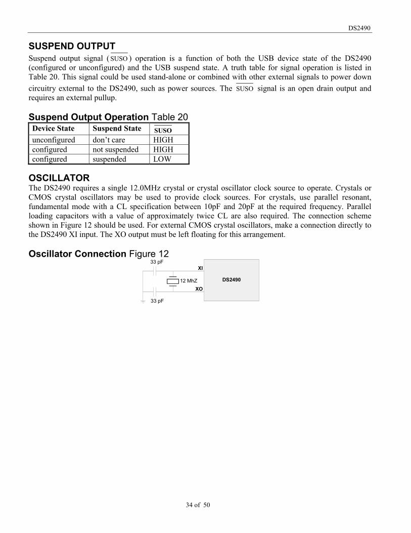
OSCILLATORThe DS2490 requires a single 12.0MHz crystal or crystal oscillator clock source to operate. Crystals orCMOS crystal oscillators may be used to provide clock sources. For crystals, use parallel resonant,fundamental mode with a CL specification between 10pF and 20pF at the required frequency. Parallelloading capacitors with a value of approximately twice CL are also required. The connection schemeshown in Figure 12 should be used. For external CMOS crystal oscillators, make a connection directly tothe DS2490 XI input. The XO output must be left floating for this arrangement.
Oscillator Connection Figure 12
DS2490
XI
XO
33 pF
33 pF
12 MhZ

DS2490
35 of 50
ABSOLUTE MAXIMUM RATINGS*Voltage on Any Pin Relative to Ground -0.5V to +6.0VOperating Temperature Range 0 oC to +70 oCStorage Temperature Range -55 oC to +125 oCSoldering Temperature See J-STD-020A Specification
• This is a stress rating only and functional operation of the device at these or any other conditions abovethose indicated in the operation sections of this specification is not implied. Exposure to absolutemaximum rating conditions for extended periods of time may affect reliability.
RECOMMENDED DC OPERATING CONDITIONSPARAMETER SYMBOL MIN MAX UNITS NOTESUSB I/F Supply Voltage VB 3.0 3.6 V 1, 3Digital Supply Voltage VD 4.4 5.5 V 1, 3EPROM Programming Supply Voltage(programming supported)
VPP 11.75 12.25 V 1, 3
EPROM Programming Supply Voltage(programming not supported)
VPP 4.4 5.5 V 1, 2, 3
Operating Temperature TA 0 70 oC
NOTES:1. Voltage referenced to ground.2. When EPROM programming is not supported VPP must be tied to VD.3. During device power-up, the supply application sequence order must be VD, VPP, VB.
DC ELECTRICAL CHARACTERISTICS TA: 0 oC to +70 oCVD: 4.4V to 5.5V, VB: 3.0V to 3.6V
PARAMETER SYMBOL MIN MAX UNITS NOTESVD Operating Current ID 20 mA 4VB Operating Current IB 7 mA 4VD Suspend Current IDS 490 µA 5VB Suspend Current IBS 10 µA 5Idle Current on VPP IPP 7.3 µA 1USB D+/- Input High VIHU 2.35 VB + 0.3 V 6USB D+/- Input Low VILU -0.3 0.7 V 61-Wire Input High VIH1 3.55 VDD + 0.3 V 61-Wire Input Low VIL1 -0.3 1.35 V 6SUSO Output Low @ 4mA VOL(SUSO) 100 mV 6
Active Pullup Timer Threshold VIAPTO VD - 1.75 VDD - 0.3 V 6Active Pullup on Threshold VIAPO 0.25 1.1 V 61-Wire Weak Pullup Current IWEAKPU 0.9 6.0 mA1-Wire Active Pullup current IACTPU 5.9 30.4 mA
DS2490
36 of 50
PARAMETER SYMBOL MIN MAX UNITS NOTESStrong Pullup Voltage Drop @ 50mAload on 1-Wire
�VSTRPU 170 1540 mV 2
Programming Voltage Drop @ 10mAload on 1-Wire
�VPROG 65 440 mV 3
VPP Sensor Trip Point VPPTRIP 6.9 10.0 V 6
NOTES:1. Applies only if 12.0V VPP supply is connected. If VPP and VD are tied together, current is less than
1�A.2. Voltage difference between VD and 1-WIRE.3. Voltage difference between VPP and 1-WIRE.4. Applies for both unconfigured and configured USB states.5. Applies for the USB suspend state.6. Voltage referenced to ground
AC CHARACTERISTICS CONDITIONS: TA: 0 oC to +70 oCVD: 4.4V to 5.5V, VB: 3.0V to 3.6V
PARAMETER SPECIFICATIONUSB I/F As defined in Chapter 7 of the USB Specification1-Wire I/F See the section “1-WIRE INTERFACE CONTROLLER” of this
document
CAPACITANCE CONDITIONS: TA: +25 oCPARAMETER SYMBOL MIN MAX UNITS NOTESInput Capacitance CIN 15 pFOutput Capacitance COUT 15 pFInput/Output Capacitance CIO 15 pF
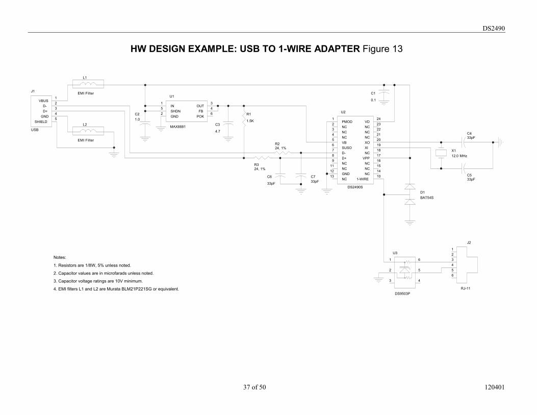
HW/SW APPLICATION RECOMMENDATIONSA schematic example of a USB to 1-Wire Adapter peripheral is shown in Figure 13.
DS2490
37 of 50 120401
HW DESIGN EXAMPLE: USB TO 1-WIRE ADAPTER Figure 13
C533pF
C6
33pF
U1
MAX8881
IN1
FB4
SHDN5
GND2
OUT3
POK6
C1
0.1
U3
DS9503P
1
2
6
5
3 4
R224, 1%
C433pF
R1
1.5K
R324, 1%
C3
4.7
X112.0 MHz
L1
EMI Filter
L2
EMI Filter
J1
USB
GND4D+3D-2VBUS1
SHIELD5
C21.0
U2
DS2490S
PMOD1
NC2
NC3
NC4
VB5
SUSO6
D-7
D+8
NC9
NC11
GND12
NC13
1-WIRE10NC14NC15NC16VPP17NC18XI19XO20NC21NC22NC23VD24
C733pF
J2
RJ-11
123456
D1BAT54S
Notes:
1. Resistors are 1/8W, 5% unless noted.
2. Capacitor values are in microfarads unless noted.
3. Capacitor voltage ratings are 10V minimum.
4. EMI filters L1 and L2 are Murata BLM21P221SG or equivalent.
DS2490
38 of 50 120401
APPENDIX 1: DS2490 CONTROL COMMANDS, SETUP PACKET ENCODING
CONTROL COMMANDSRESET DEVICE
Setup Packet Encoding:bmRequestType 0x40
bRequest CONTROL_CMDwValue CTL_RESET_DEVICEwIndex 0x0000
wLength 0x0000
START EXECUTIONSetup Packet Encoding:
bmRequestType 0x40bRequest CONTROL_CMD
wValue CTL_START_EXEwIndex 0x0000
wLength 0x0000
RESUME EXECUTIONSetup Packet Encoding:
bmRequestType 0x40bRequest CONTROL_CMD
wValue CTL_RESUME_EXEwIndex 0x0000
wLength 0x0000
HALT EXECUTION WHENIDLE
Setup Packet Encoding:bmRequestType 0x40
bRequest CONTROL_CMDwValue CTL_HALT_EXE_IDLEwIndex 0x0000
wLength 0x0000
HALT EXECUTION WHENDONE
Setup Packet Encoding:bmRequestType 0x40
bRequest CONTROL_CMDwValue CTL_HALT_EXE_DONEwIndex 0x0000

DS2490
39 of 50
CONTROL COMMANDSwLength 0x0000
FLUSH COMM CMDS The DS2490 must be in a halted state before the FLUSH COMMCMDS command can be processed.
Setup Packet Encoding:bmRequestType 0x40
bRequest CONTROL_CMDwValue CTL_FLUSH_COMM_CMDSwIndex 0x0000
wLength 0x0000
FLUSH DATA RCVBUFFER
The DS2490 must be in a halted state before the FLUSH DATARCV BUFFER command can be processed.
Setup Packet Encoding:bmRequestType 0x40
bRequest CONTROL_CMDwValue CTL_FLUSH_RCV_BUFFERwIndex 0x0000
wLength 0x0000
FLUSH DATA XMTBUFFER
The DS2490 must be in a halted state before the FLUSH DATAXMT BUFFER command can be processed.
Setup Packet Encoding:bmRequestType 0x40
bRequest CONTROL_CMDwValue CTL_FLUSH_XMT_BUFFERwIndex 0x0000
wLength 0x0000
GET COMM CMDS The DS2490 must be in a halted state before the GET COMMCMDS command can be processed.
Setup Packet Encoding:bmRequestType 0xC0
bRequest CONTROL_CMDwValue CTL_GET_COMM_CMDSwIndex 0x0000
wLength variableThe value of the wLength field depends on the number ofcommunication commands and parameters loaded in the FIFO.

DS2490
40 of 50
APPENDIX 2: DS2490 COMMUNICATION COMMANDS, EMBEDDED COMMAND BITS, SETUPPACKET ENCODING.
Communication commands contain embedded command parameter bits in the wValue field. Thedefinitions of bit parameters are described below.
BIT NAME DESCRIPTIONCH CH = 1 follows the chain if the page is redirected.
CH = 0 stops reading if the page is redirected.CIB CIB = 1 prevents a strong pullup to 5V if SPU = 1 and the bit read back from the 1-
Wire bus is 1.CIB = 0 generally enables the strong pullup to 5V.
PS PS = 1 reduces the preamble size to 2 bytes (rather than 3).PS = 0 sets preamble size to 3 bytes.
D Data bit value to be written to the 1-Wire bus.DT DT = 1 activates/selects the CRC16 generator
DT = 0 specifies no CRC.F F = 1 clears the buffers in case an error occurred during the execution of the previous
command; requires that ICP = 0 in the previous command.F = 0 prevents the buffers from being cleared.
ICP ICP = 1 indicates that the command is not the last one of a macro; as a consequencecommand processing result feedback messages are suppressed.ICP = 0 indicates that the command is the last one of a macro or single commandoperation; enables command processing result feedback signaling.
IM IM = 1 enables immediate execution of the command. Assumes that all 1-Wire devicedata required by the command has been received at EP2.IM = 0 prevents immediate execution of the command; execution must be startedthrough a control function command.
NTF NTF = 1 always generate communication command processing result feedback if ICP =0NTF = 0 generate communication command processing result feedback only if an erroroccurs and ICP = 0.If ICP = 1 command result feedback is suppressed for either case, see the ICP bit above.
PST PST = 1 continuously generate 1-Wire Reset sequences until a presence pulse isdiscovered.PST = 0 generate only one 1-Wire Reset sequence.
R R = 1 performs a read function.R = 0 performs a write function.
RST RST = 1 inserts a 1-Wire Reset before executing the command.RST = 0 no 1-Wire Reset inserted.
RTS RTS = 1 returns the discrepancy information to the host if SM = 1 and there are moredevices than could be discovered in the current pass.RTS = 0 does not return discrepancy information.
SE SE = 1 enable the speed change on the 1-Wire bus.SE = 0 disable the speed change on the 1-Wire bus.

DS2490
41 of 50
SM SM = 1 searches for and reports ROM Ids without really accessing a particular device.SM = 0 makes a “Strong Access” to a particular device.
SPU SPU = 1 inserts a strong pullup to 5V after a Bit or Byte or Block I/O or Do & Releasecommand.SPU = 0 no strong pullup.
TYPE TYPE = 1 specifies programming pulse duration.TYPE = 0 specifies strong pullup duration.
Z Z = 1 checks if the 0-bits in the byte to be written are 0-bits in the byte read back formthe device.Z = 0 checks if the byte to be written is identical to the one read back from the device.
COMMUNICATION COMMANDSSET DURATION
Setup Packet Encoding:bmRequestType 0x40
bRequest COMM_CMDwValue byte 2 byte 1
byte 2: 0 0 0 0 0 NTF ICP 0byte 1: 0 0 0 1 TYPE 0 1 IM
wIndex byte 2 byte 1byte 2 – 0x00 (unused)byte 1 – new duration:Unsigned 8-bit binary number specifying the new duration. SeeMODE CONTROL section for byte bit weighting and additionalformat information.
wLength 0x0000
PULSESetup Packet Encoding:
bmRequestType 0x40bRequest COMM_CMD
wValue byte 2 byte 1byte 2: 0 0 0 0 F NTF ICP 0byte 1: 0 0 1 1 TYPE 0 0 IM
wIndex 0x0000wLength 0x0000
1-WIRE RESETSetup Packet Encoding:
bmRequestType 0x40bRequest COMM_CMD
wValue byte 2 byte 1byte 2: 0 PST 0 0 F NTF ICP 0

DS2490
42 of 50
COMMUNICATION COMMANDSbyte 1: 0 1 0 0 SE 0 1 IM
wIndex byte 2 byte 1byte 2 – 0x00 (unused)byte 1 – new speed:0x02 with SE = 1 after Overdrive Skip ROM0x01 or 0x00 with SE = 1 in all other casesdon’t care with SE = 0
wLength 0x0000
BIT I/OSetup Packet Encoding:
bmRequestType 0x40bRequest COMM_CMD
wValue byte 2 byte 1byte 2: 0 CIB 0 SPU 0 NTF ICP 0byte 1: 0 0 1 0 D 0 0 IM
wIndex byte 2 byte 1byte 2 – 0x00 (unused)byte 1 – 0x00 (unused)
wLength 0x0000
BYTE I/OSetup Packet Encoding:
bmRequestType 0x40bRequest COMM_CMD
wValue byte 2 byte 1byte 2: 0 0 0 SPU 0 NTF ICP 0byte 1: 0 1 0 1 0 0 1 IM
wIndex byte 2 byte 1byte 2 – 0x00 (unused)byte 1 – data byte to be sent to the 1-Wire bus. To read only, the byteshould be 0xFF.
wLength 0x0000
BLOCK I/OSetup Packet Encoding:
bmRequestType 0x40bRequest COMM_CMD
wValue byte 2 byte 1byte 2: 0 0 0 SPU 0 NTF ICP RSTbyte 1: 0 1 1 1 0 1 0 IM
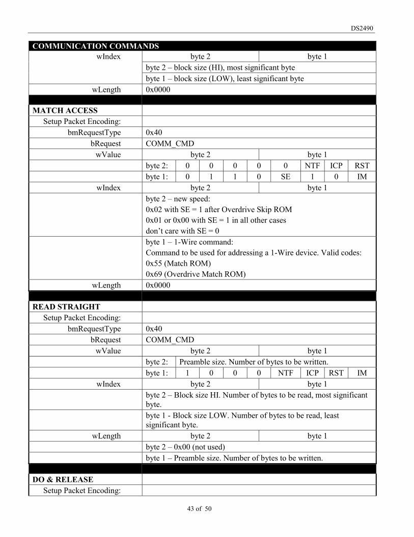
DS2490
43 of 50
COMMUNICATION COMMANDSwIndex byte 2 byte 1
byte 2 – block size (HI), most significant bytebyte 1 – block size (LOW), least significant byte
wLength 0x0000
MATCH ACCESSSetup Packet Encoding:
bmRequestType 0x40bRequest COMM_CMD
wValue byte 2 byte 1byte 2: 0 0 0 0 0 NTF ICP RSTbyte 1: 0 1 1 0 SE 1 0 IM
wIndex byte 2 byte 1byte 2 – new speed:0x02 with SE = 1 after Overdrive Skip ROM0x01 or 0x00 with SE = 1 in all other casesdon’t care with SE = 0byte 1 – 1-Wire command:Command to be used for addressing a 1-Wire device. Valid codes:0x55 (Match ROM)0x69 (Overdrive Match ROM)
wLength 0x0000
READ STRAIGHTSetup Packet Encoding:
bmRequestType 0x40bRequest COMM_CMD
wValue byte 2 byte 1byte 2: Preamble size. Number of bytes to be written.byte 1: 1 0 0 0 NTF ICP RST IM
wIndex byte 2 byte 1byte 2 – Block size HI. Number of bytes to be read, most significantbyte.byte 1 - Block size LOW. Number of bytes to be read, leastsignificant byte.
wLength byte 2 byte 1byte 2 – 0x00 (not used)byte 1 – Preamble size. Number of bytes to be written.
DO & RELEASESetup Packet Encoding:
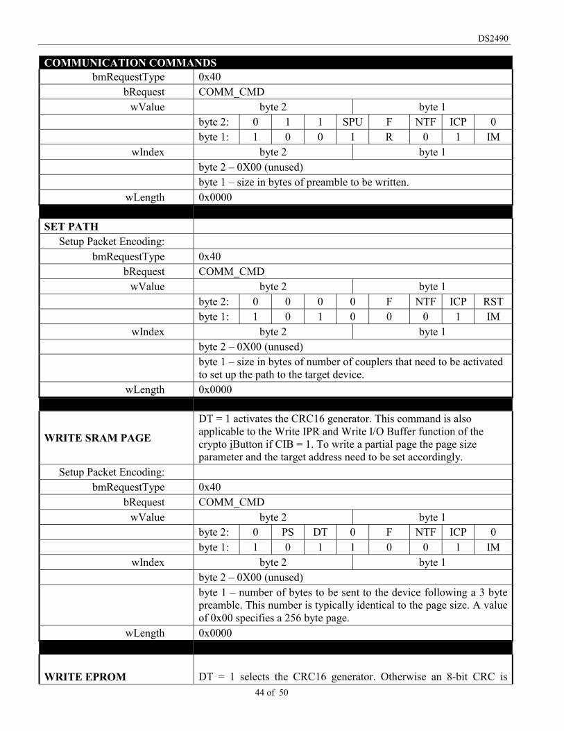
DS2490
44 of 50
COMMUNICATION COMMANDSbmRequestType 0x40
bRequest COMM_CMDwValue byte 2 byte 1
byte 2: 0 1 1 SPU F NTF ICP 0byte 1: 1 0 0 1 R 0 1 IM
wIndex byte 2 byte 1byte 2 – 0X00 (unused)byte 1 – size in bytes of preamble to be written.
wLength 0x0000
SET PATHSetup Packet Encoding:
bmRequestType 0x40bRequest COMM_CMD
wValue byte 2 byte 1byte 2: 0 0 0 0 F NTF ICP RSTbyte 1: 1 0 1 0 0 0 1 IM
wIndex byte 2 byte 1byte 2 – 0X00 (unused)byte 1 – size in bytes of number of couplers that need to be activatedto set up the path to the target device.
wLength 0x0000
WRITE SRAM PAGE
DT = 1 activates the CRC16 generator. This command is alsoapplicable to the Write IPR and Write I/O Buffer function of thecrypto iButton if CIB = 1. To write a partial page the page sizeparameter and the target address need to be set accordingly.
Setup Packet Encoding:bmRequestType 0x40
bRequest COMM_CMDwValue byte 2 byte 1
byte 2: 0 PS DT 0 F NTF ICP 0byte 1: 1 0 1 1 0 0 1 IM
wIndex byte 2 byte 1byte 2 – 0X00 (unused)byte 1 – number of bytes to be sent to the device following a 3 bytepreamble. This number is typically identical to the page size. A valueof 0x00 specifies a 256 byte page.
wLength 0x0000
WRITE EPROM DT = 1 selects the CRC16 generator. Otherwise an 8-bit CRC is

DS2490
45 of 50
COMMUNICATION COMMANDSassumed. If Z = 1 the comparison of the byte read back forverification is limited to 0 bits only.
Setup Packet Encoding:bmRequestType 0x40
bRequest COMM_CMDwValue byte 2 byte 1
byte 2: 0 0 DT 0 F NTF ICP 0byte 1: 1 1 0 0 Z 1 0 IM
wIndex byte 2 byte 1byte 2 – block size (HI), number of bytes to be written, mostsignificant bytebyte 1 – block size (LOW), number of bytes to be written, leastsignificant byte
wLength 0x0000
READ CRC PROT PAGEDT = 1 selects the CRC16 generator, otherwise an 8-bit CRC isassumed. This command is also applicable to the Read IPR and ReadI/O Buffer function of the crypto iButton if CIB = 1.
Setup Packet Encoding:bmRequestType 0x40
bRequest COMM_CMDwValue byte 2 byte 1
byte 2: 0 PS DT 0 F NTF ICP 0byte 1: 1 1 0 1 0 1 0 IM
wIndex byte 2 byte 1byte 2 –number of pages to be read.byte 1 – page size: log(base 2) of the number of bytes that areconsidered a page. Typical is 32-decimal for data memory and 8 forstatus memory. Page size 0 indicates a 256-byte page. As anexample, if the actual page size is 3210, then the Page Size parameterwould need to be 0x05
wLength 0x0000
READ REDIRECT PAGEW/CRC
Setup Packet Encoding:bmRequestType 0x40
bRequest COMM_CMDwValue byte 2 byte 1
byte 2: 0 0 1 0 F NTF ICP 1byte 1: 1 1 1 0 CH 1 0 IM
wIndex byte 2 byte 1

DS2490
46 of 50
COMMUNICATION COMMANDSbyte 2 - page number to be used for the first read attempt.byte 1 – page size: number of bytes that are considered a page.Typical is 32 decimal for data memory. Page size 0 indicates a 256-byte page.
wlength 0x0000
SEARCH ACCESSSetup Packet Encoding:
bmRequestType 0x40bRequest COMM_CMD
wValue byte 2 byte 1byte 2: 0 RTS 0 0 F NTF ICP RSTbyte 1: 1 1 1 1 SM 1 0 IM
wIndex byte 2 byte 1byte 2 – number of devices. Maximum number of devices to bediscovered in a single command call. A value of 0x00 indicates thatall devices on the 1-Wire Network are to be discovered.byte 1 – 1-Wire command:Command to be used for addressing a 1-Wire device. Valid codes:0xF0 (Search ROM)0xEC (Conditional Search ROM)
wLength 0x0000

DS2490
47 of 50
APPENDIX 3: DS2490 MODE COMMANDS, SETUP PACKET ENCODING
MODE COMMANDSENABLE PULSE
Setup Packet Encoding:bmRequestType 0x40
bRequest MODE_CMDwValue MOD_PULSE_ENwIndex byte 2 byte 1
byte 2 – 0x00byte 1: 0 0 0 0 0 0 SPUE PRGEStrong pullup is enabled with SPUE = 1, disabled with SPUE = 0.+12V Programming pulse is enabled with PRGE = 1, disabled with PRGE= 0.
wLength 0x0000
ENABLE SPEED CHANGESetup Packet Encoding:
bmRequestType 0x40bRequest MODE_CMD
wValue MOD_SPEED_CHANGE_ENwIndex byte 2 byte 1
byte 2 – 0x00byte 1 – Boolean value. Speed changes are enabled with TRUE, disabledwith FALSE.
wLength 0x0000
1-WIRE SPEEDSetup Packet Encoding:
bmRequestType 0x40bRequest MODE_CMD
wValue MOD_1WIRE_SPEEDwIndex byte 2 byte 1
byte 2 – 0x00byte 1 – 1-Wire speed:Code specifying communication speed of the 1-Wire bus. See MODECONTROL section for code definition.
wLength 0x0000
STRONG PULLUPDURATION
Setup Packet Encoding:bmRequestType 0x40
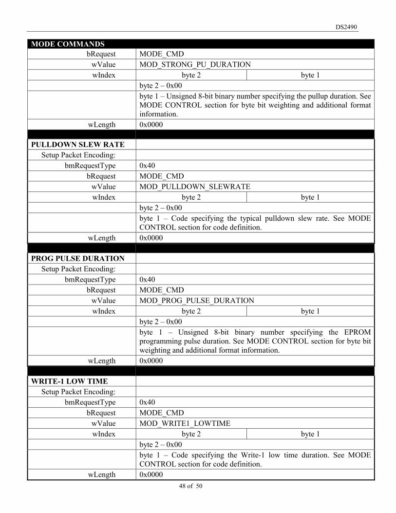
DS2490
48 of 50
MODE COMMANDSbRequest MODE_CMD
wValue MOD_STRONG_PU_DURATIONwIndex byte 2 byte 1
byte 2 – 0x00byte 1 – Unsigned 8-bit binary number specifying the pullup duration. SeeMODE CONTROL section for byte bit weighting and additional formatinformation.
wLength 0x0000
PULLDOWN SLEW RATESetup Packet Encoding:
bmRequestType 0x40bRequest MODE_CMD
wValue MOD_PULLDOWN_SLEWRATEwIndex byte 2 byte 1
byte 2 – 0x00byte 1 – Code specifying the typical pulldown slew rate. See MODECONTROL section for code definition.
wLength 0x0000
PROG PULSE DURATIONSetup Packet Encoding:
bmRequestType 0x40bRequest MODE_CMD
wValue MOD_PROG_PULSE_DURATIONwIndex byte 2 byte 1
byte 2 – 0x00byte 1 – Unsigned 8-bit binary number specifying the EPROMprogramming pulse duration. See MODE CONTROL section for byte bitweighting and additional format information.
wLength 0x0000
WRITE-1 LOW TIMESetup Packet Encoding:
bmRequestType 0x40bRequest MODE_CMD
wValue MOD_WRITE1_LOWTIMEwIndex byte 2 byte 1
byte 2 – 0x00byte 1 – Code specifying the Write-1 low time duration. See MODECONTROL section for code definition.
wLength 0x0000
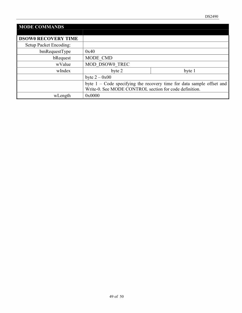
DS2490
49 of 50
MODE COMMANDS
DSOW0 RECOVERY TIMESetup Packet Encoding:
bmRequestType 0x40bRequest MODE_CMD
wValue MOD_DSOW0_TRECwIndex byte 2 byte 1
byte 2 – 0x00byte 1 – Code specifying the recovery time for data sample offset andWrite-0. See MODE CONTROL section for code definition.
wLength 0x0000
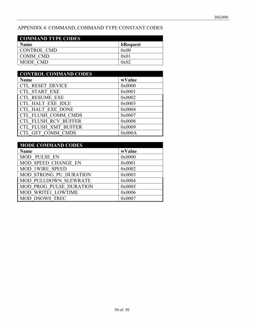
DS2490
50 of 50
APPENDIX 4: COMMAND, COMMAND TYPE CONSTANT CODES
COMMAND TYPE CODESName bRequestCONTROL_CMD 0x00COMM_CMD 0x01MODE_CMD 0x02
CONTROL COMMAND CODESName wValueCTL_RESET_DEVICE 0x0000CTL_START_EXE 0x0001CTL_RESUME_EXE 0x0002CTL_HALT_EXE_IDLE 0x0003CTL_HALT_EXE_DONE 0x0004CTL_FLUSH_COMM_CMDS 0x0007CTL_FLUSH_RCV_BUFFER 0x0008CTL_FLUSH_XMT_BUFFER 0x0009CTL_GET_COMM_CMDS 0x000A
MODE COMMAND CODESName wValueMOD_ PULSE_EN 0x0000MOD_SPEED_CHANGE_EN 0x0001MOD_1WIRE_SPEED 0x0002MOD_STRONG_PU_DURATION 0x0003MOD_PULLDOWN_SLEWRATE 0x0004MOD_PROG_PULSE_DURATION 0x0005MOD_WRITE1_LOWTIME 0x0006MOD_DSOW0_TREC 0x0007