ds80pci402 2.5-gbps / 5.0-gbps / 8.0-gbps 4-lane … · ds80pci402 snls324e –april 2011–revised...
TRANSCRIPT
VDD (2.5 V)
INA_0+INA_0-
AD0
AD1
AD2
AD3
ENSMB
SCL(2)
READ_EN
SDA(2)
OUTA_0+OUTA_0-
.
.
.
.
.
.
GND (DAP)
(1) Schematic shows connection for SMBus Slave Mode (ENSMB=1k to VDD) For SMBus Master Mode or Pin Mode configuration, the connections are different.(2) SMBus signals need to be pulled up elsewhere in the system.(3) Schematic requires different connections for 2.5 V mode.
.
.
.
VIN
0.1�F (x5)
SMBus Slave Mode(1)
.
.
.
INA_3+INA_3-
OUTA_3+OUTA_3-
SMBus Slave Mode(1)
VDD_SEL
VIN (3.3 V)
INB_0+INB_0-
OUTB_0+OUTB_0-...
.
.
.
.
.
.
.
.
.
INB_3+INB_3-
OUTB_3+OUTB_3-
RXDET
RATE
PRSNTFrom PCIe PRSNT signal
Address straps(pull-up to VIN or
pull-down to GND)(1)
1�F
3.3V(3)
10�F
ALL_DONESMBus Slave Mode(1)
LPBK
To SMBus/I2CHost Controller
DS80PCI402
.
.
.
.
.
.
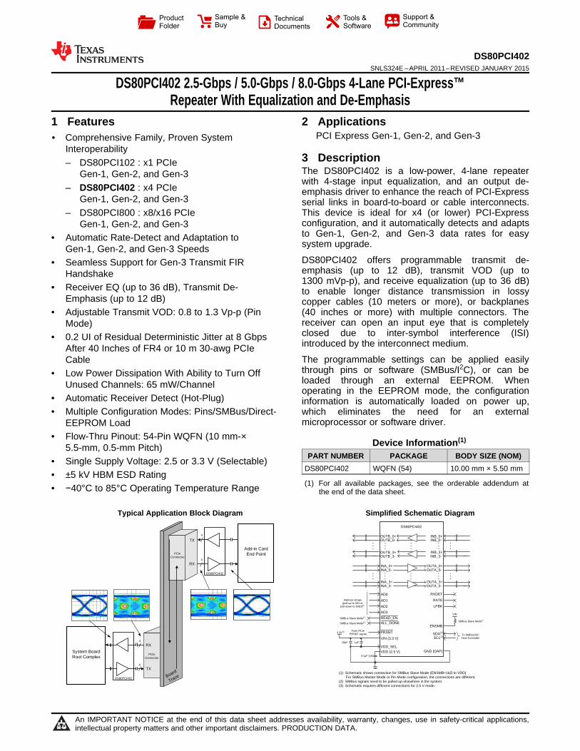
DS80PCI402
System BoardRoot Complex
Add-in CardEnd Point
DS80PCI402
Board
Trace
PCIeConnector
PCIeConnector
TX
RX
RX
TX4
4
4
4
Product
Folder
Sample &Buy
Technical
Documents
Tools &
Software
Support &Community
DS80PCI402SNLS324E –APRIL 2011–REVISED JANUARY 2015
DS80PCI402 2.5-Gbps / 5.0-Gbps / 8.0-Gbps 4-Lane PCI-Express™Repeater With Equalization and De-Emphasis
1 Features 2 ApplicationsPCI Express Gen-1, Gen-2, and Gen-3
1• Comprehensive Family, Proven SystemInteroperability
3 Description– DS80PCI102 : x1 PCIeThe DS80PCI402 is a low-power, 4-lane repeaterGen-1, Gen-2, and Gen-3with 4-stage input equalization, and an output de-
– DS80PCI402 : x4 PCIe emphasis driver to enhance the reach of PCI-ExpressGen-1, Gen-2, and Gen-3 serial links in board-to-board or cable interconnects.
This device is ideal for x4 (or lower) PCI-Express– DS80PCI800 : x8/x16 PCIeconfiguration, and it automatically detects and adaptsGen-1, Gen-2, and Gen-3to Gen-1, Gen-2, and Gen-3 data rates for easy• Automatic Rate-Detect and Adaptation tosystem upgrade.Gen-1, Gen-2, and Gen-3 SpeedsDS80PCI402 offers programmable transmit de-• Seamless Support for Gen-3 Transmit FIRemphasis (up to 12 dB), transmit VOD (up toHandshake1300 mVp-p), and receive equalization (up to 36 dB)
• Receiver EQ (up to 36 dB), Transmit De- to enable longer distance transmission in lossyEmphasis (up to 12 dB) copper cables (10 meters or more), or backplanes
• Adjustable Transmit VOD: 0.8 to 1.3 Vp-p (Pin (40 inches or more) with multiple connectors. Thereceiver can open an input eye that is completelyMode)closed due to inter-symbol interference (ISI)• 0.2 UI of Residual Deterministic Jitter at 8 Gbpsintroduced by the interconnect medium.After 40 Inches of FR4 or 10 m 30-awg PCIeThe programmable settings can be applied easilyCablethrough pins or software (SMBus/I2C), or can be• Low Power Dissipation With Ability to Turn Offloaded through an external EEPROM. WhenUnused Channels: 65 mW/Channel operating in the EEPROM mode, the configuration
• Automatic Receiver Detect (Hot-Plug) information is automatically loaded on power up,• Multiple Configuration Modes: Pins/SMBus/Direct- which eliminates the need for an external
microprocessor or software driver.EEPROM Load• Flow-Thru Pinout: 54-Pin WQFN (10 mm-× Device Information(1)
5.5-mm, 0.5-mm Pitch)PART NUMBER PACKAGE BODY SIZE (NOM)• Single Supply Voltage: 2.5 or 3.3 V (Selectable)
DS80PCI402 WQFN (54) 10.00 mm × 5.50 mm• ±5 kV HBM ESD Rating
(1) For all available packages, see the orderable addendum at• −40°C to 85°C Operating Temperature Range the end of the data sheet.
Typical Application Block Diagram Simplified Schematic Diagram
1
An IMPORTANT NOTICE at the end of this data sheet addresses availability, warranty, changes, use in safety-critical applications,intellectual property matters and other important disclaimers. PRODUCTION DATA.
DS80PCI402SNLS324E –APRIL 2011–REVISED JANUARY 2015 www.ti.com
Table of Contents8.4 Device Functional Modes........................................ 161 Features .................................................................. 18.5 Programming........................................................... 162 Applications ........................................................... 18.6 Register Maps ......................................................... 203 Description ............................................................. 1
9 Application and Implementation ........................ 404 Revision History..................................................... 29.1 Application Information............................................ 405 Pin Configuration and Functions ......................... 39.2 Typical Application ................................................. 416 Specifications......................................................... 6
10 Power Supply Recommendations ..................... 436.1 Absolute Maximum Ratings ..................................... 610.1 3.3-V or 2.5-V Supply Mode Operation................. 436.2 ESD Ratings.............................................................. 610.2 Power Supply Bypassing ...................................... 446.3 Recommended Operating Ratings............................ 6
11 Layout................................................................... 456.4 Thermal Information .................................................. 611.1 Layout Guidelines ................................................. 456.5 Electrical Characteristics........................................... 711.2 Layout Example .................................................... 456.6 Electrical Characteristics — Serial Management Bus
Interface .................................................................. 10 12 Device and Documentation Support ................. 466.7 Typical Characteristics ............................................ 11 12.1 Device Support...................................................... 46
12.2 Trademarks ........................................................... 467 Parameter Measurement Information ................ 1212.3 Electrostatic Discharge Caution............................ 468 Detailed Description ............................................ 1312.4 Glossary ................................................................ 468.1 Overview ................................................................. 13
13 Mechanical, Packaging, and Orderable8.2 Functional Block Diagram ....................................... 13Information ........................................................... 468.3 Feature Description................................................. 14
4 Revision HistoryNOTE: Page numbers for previous revisions may differ from page numbers in the current version.
Changes from Revision D (April 2013) to Revision E Page
• Added ESD Ratings table, Feature Description section, Device Functional Modes, Application and Implementationsection, Power Supply Recommendations section, Layout section, Device and Documentation Support section, andMechanical, Packaging, and Orderable Information section .................................................................................................. 1
Changes from Revision C (April 2013) to Revision D Page
• Changed layout of National Data Sheet to TI format ........................................................................................................... 42
2 Submit Documentation Feedback Copyright © 2011–2015, Texas Instruments Incorporated
Product Folder Links: DS80PCI402

OUTB_0+
OUTB_0-
OUTB_1+
LPB
K
RX
DE
T
ALL
_DO
NE
1
2
3
4
2625
DAP = GND
OUTB_1-
OUTB_2+
OUTB_2-
5
6
7
242120 23
INA_3-
8
INA_0+
INA_0-
VDD
INA_1+
9
10
11
12
INA_1-
EQ
A0
INA_2+
INA_2-
13
18
14
15
INA_3+
16
17
OUTA_1+
OUTA_1-
EQ
A1
OUTA_2+
36
34
35
OUTA_2-
OUTA_3+
OUTA_3-
33
31
32
VIN
VD
D_S
EL
INB_3+
INB_3-
VDD
41
40
39
RA
TE
OUTA_0+
OUTA_0-
37
38
INB_0+
INB_0-
INB_1+
INB_1-
INB_2-
INB_2+
44
42
43V
DD
DE
MA
1/S
CL
50 48 4749D
EM
A0/
SD
A
EN
SM
B
4651
OUTB_3+
OUTB_3-
SMBUS AND CONTROL
DE
MB
1/A
D0
DE
MB
0/A
D1
30
29
28
SD
_TH
/RE
AD
_EN
52
EQ
B1/
AD
2
EQ
B0/
AD
3
19 22
PR
SN
T
27
455354
VDD
VDD
`
DS80PCI402www.ti.com SNLS324E –APRIL 2011–REVISED JANUARY 2015
5 Pin Configuration and Functions
DS80PCI40254 Pins
Top View
Copyright © 2011–2015, Texas Instruments Incorporated Submit Documentation Feedback 3
Product Folder Links: DS80PCI402
DS80PCI402SNLS324E –APRIL 2011–REVISED JANUARY 2015 www.ti.com
Pin Functions (1) (2) (3) (4)
PINI/O, TYPE DESCRIPTION
NAME NUMBERDIFFERENTIAL HIGH SPEED I/OsOUTB_0+, OUTB_0-,OUTB_1+, OUTB_1-, 1, 2, 3, 4, Inverting and non-inverting 50-Ω driver bank B outputs with de-emphasis. CompatibleIOUTB_2+, OUTB_2-, 5, 6, 7, 8 with AC-coupled CML inputs.OUTB_3+, OUTB_3-INA_0+, INA_0-, Inverting and non-inverting differential inputs to bank A equalizer. A gated on-chip 50-Ω10, 11, 12,INA_1+, INA_1-, termination resistor connects INA_n+ to VDD and INA_n- to VDD depending on the state13, 15, 16, IINA_2+, INA_2-, of RXDET. See Table 417, 18INA_3+, INA_3- AC coupling required on high-speed I/OINB_0+, INB_0-, Inverting and non-inverting differential inputs to bank B equalizer. A gated on-chip 50-Ω45, 44, 43,INB_1+, INB_1-, termination resistor connects INB_n+ to VDD and INB_n- to VDD depending on the state42, 40, 39, OINB_2+, INB_2-, of RXDET. See Table 438, 37INB_3+, INB_3- AC coupling required on high-speed I/OOUTA_0+, OUTA_0-, 35, 34, 33,OUTA_1+, OUTA_1-, Inverting and non-inverting 50-Ω driver bank A outputs with de-emphasis. Compatible32, 31, 30, OOUTA_2+, OUTA_2-, with AC-coupled CML inputs.29, 28OUTA_3+, OUTA_3-CONTROL PINS — SHARED (LVCMOS)
System management bus (SMBus) enable pinTie 1 kΩ to VDD (2.5-V mode) or VIN (3.3-V mode) = Register access SMBus slaveI, 4-LEVEL,ENSMB 48 modeLVCMOS FLOAT = Read external EEPROM (master SMBUS mode)Tie 1 kΩ to GND = Pin mode
ENSMB = 1 (SMBus SLAVE MODE)I, 2-LEVEL, In SMBus Slave Mode, this pin is the SMBus clock I/O. Clock input or open drain output.LVCMOS,SCL 50 External 2-kΩ to 5-kΩ pullup resistor to VDD or VIN recommended as per SMBusO, open interface standards (5)
drainI, 2-LEVEL, In both SMBus Modes, this pin is the SMBus data I/O. Data input or open drain output.LVCMOS,SDA 49 External 2-kΩ to 5-kΩ pullup resistor to VDD or VIN recommended as per SMBusO, open interface standards (5)
drainSMBus Slave Address Inputs. In both SMBus Modes, these pins are the user set SMBus54, 53, 47, I, 4-LEVEL,AD0-AD3 slave address inputs.46 LVCMOS External 1-kΩ pullup or pulldown recommended.
READ_EN / SD_TH 26 I, FLOAT In SMBus Slave Mode, this pin is not used. Leave it floating.ENSMB = FLOAT (SMBus MASTER MODE)
I, 2-LEVEL, Clock output when loading EEPROM configuration, reverting to SMBus clock input whenLVCMOS, EEPROM load is complete (ALL_DONE = 0).SCL 50 O, open External 2-kΩ to 5-kΩ pullup resistor to VDD or VIN recommended as per SMBus
drain interface standards (5)
I, 2-LEVEL, In both SMBus Modes, this pin is the SMBus data I/O. Data input or open drain output.LVCMOS,SDA 49 External 2-kΩ to 5-kΩ pullup resistor to VDD or VIN recommended as per SMBusO, open interface standards (5)drain
SMBus Slave Address Inputs. In both SMBus Modes, these pins are the user set SMBus54, 53, 47, I, 4-LEVEL,AD0-AD3 slave address inputs.46 LVCMOS External 1-kΩ pullup or pulldown recommended.A logic low on this pin starts the load from the external EEPROM (6)
I, 2-LEVEL,READ_EN 26 Once EEPROM load is complete (ALL_DONE = 0), this pin functionality remains asLVCMOS READ_EN. It does not revert to an SD_TH input.
(1) LVCMOS inputs without the “FLOAT” conditions must be driven to a logic low or high at all times or operation is not verified.(2) Input edge rate for LVCMOS/FLOAT inputs must be faster than 50 ns from 10% to 90%.(3) For 3.3-V mode operation, VIN pin = 3.3 V and the VDD for the 4-level input is 3.3 V.(4) For 2.5-V mode operation, VDD pin = 2.5 V and the VDD for the 4-level input is 2.5 V.(5) SCL and SDA pins can be tied either to 3.3 V or 2.5 V, regardless of whether the device is operating in 2.5-V mode or 3.3-V mode.(6) When READ_EN is asserted low, the device attempts to load EEPROM. If EEPROM cannot be loaded successfully, for example due to
an invalid or blank hex file, the DS80PCI402 waits indefinitely in an unknown state where SMBus access is not possible. ALL_DONE pinremains high in this situation.
4 Submit Documentation Feedback Copyright © 2011–2015, Texas Instruments Incorporated
Product Folder Links: DS80PCI402

DS80PCI402www.ti.com SNLS324E –APRIL 2011–REVISED JANUARY 2015
Pin Functions(1)(2)(3)(4) (continued)PIN
I/O, TYPE DESCRIPTIONNAME NUMBER
O, 2- Valid register load status outputALL_DONE 27 LEVEL, HIGH = External EEPROM load failed or incomplete
LVCMOS LOW = External EEPROM load passedENSMB = 0 (PIN MODE)
EQA[1:0] and EQB[1:0] control the level of equalization on the input pins. The pins areactive only when ENSMB is deasserted (low). The 8 channels are organized into two
EQA0, EQA1, 20, 19, 46, I, 4-LEVEL, banks. Bank A is controlled with the EQA[1:0] pins and bank B is controlled with theEQB0, EQB1 47 LVCMOS EQB[1:0] pins. When ENSMB goes high the SMBus registers provide independent
control of each channel. The EQB[1:0] pins are converted to SMBUS AD2/AD3 inputs.See Table 2.DEMA[1:0] and DEMB[1:0] control the level of de-emphasis of the output driver. Thepins are only active when ENSMB is deasserted (low). The 8 channels are organizedinto two banks. Bank A is controlled with the DEMA[1:0] pins and bank B is controlledDEMA0, DEMA1, 49, 50, 53, I, 4-LEVEL, with the DEMB[1:0] pins. When ENSMB goes high the SMBus registers provideDEMB0, DEMB1 54 LVCMOS independent control of each channel. The DEMA[1:0] pins are converted to SMBUSSCL/SDA and DEMB[1:0] pins are converted to AD0, AD1 inputs.See Table 3.
CONTROL PINS — BOTH PIN AND SMBUS MODES (LVCMOS)RATE control pin selects GEN 1,2 and GEN 3 operating modes.Tie 1 kΩ to GND = GEN 1,2I, 4-LEVEL,RATE 21 FLOAT = AUTO Rate Select of Gen1/2 and Gen3 with de-emphasisLVCMOS Tie 20 kΩ to GND = GEN 3 without de-emphasisTied 1 kΩ to VDD = RESERVEDThe RXDET pin controls the receiver detect function. Depending on the input level, a 50-I, 4-LEVEL,RXDET 22 Ω or > 50-kΩ termination to the power rail is enabled.LVCMOS See Table 4.Controls the loopback function
I, 4-LEVEL, Tie 1 kΩ to GND = Root Complex Loopback (INA_n to OUTB_n)LPBK 23 LVCMOS Float = Normal OperationTie 1 kΩ to VDD = End-point Loopback (INB_n to OUTA_n)Controls the internal regulatorFLOAT = 2.5-V modeVDD_SEL 25 I, LVCMOS Tie GND = 3.3-V modeSee Figure 14.
I, 4-LEVEL, Controls the internal Signal Detect Threshold.SD_TH 26 LVCMOS See Table 5.Cable Present Detect input. High when a cable is not present per PCIe Cabling Spec.I, 2-LEVEL,PRSNT 52 1.0. Puts part into low power mode. When LOW (normal operation) part is enabled.LVCMOS See Table 4.
POWERIn 3.3-V mode, feed 3.3 V to VINVIN 24 Power In 2.5-V mode, leave floatingPower supply pins9, 14, 36,VDD Power 2.5-V mode, connect to 2.5-V supply41, 51 3.3-V mode, connect 0.1-µF capacitor to each VDD pin (output of LDO)
GND DAP Power Ground pad (DAP - die attach pad)
Copyright © 2011–2015, Texas Instruments Incorporated Submit Documentation Feedback 5
Product Folder Links: DS80PCI402

DS80PCI402SNLS324E –APRIL 2011–REVISED JANUARY 2015 www.ti.com
6 Specifications
6.1 Absolute Maximum Ratings (1) (2) (3)
MIN MAX UNITSupply Voltage (VDD - 2.5 V) –0.5 2.75 VSupply Voltage (VIN - 3.3 V) –0.5 4.0 VLVCMOS input/output voltage –0.5 4.0 VCML Input Voltage –0.5 VDD + 0.5 VCML Input Current –30 30 mAJunction Temperature 125 °CLead Temperature Soldering (4 s) (4) 260 °CStorage temperature, Tstg –40 125 °C
(1) Stresses beyond those listed under Absolute Maximum Ratings may cause permanent damage to the device. These are stress ratingsonly, and functional operation of the device at these or any other conditions beyond those indicated under Recommended OperatingRatings is not implied. Exposure to absolute-maximum-rated conditions for extended periods may affect device reliability.
(2) Absolute Maximum Numbers are specified for a junction temperature range of –40° C to 125° C. Models are validated to MaximumOperating Voltages only.
(3) If Military/Aerospace specified devices are required, please contact the Texas Instruments Sales Office/ Distributors for availability andspecifications.
(4) For soldering specifications: See application note SNOA549.
6.2 ESD RatingsVALUE UNIT
Human body model (HBM), per ANSI/ESDA/JEDEC JS-001, all pins (1) ±5000Charged device model (CDM), per JEDEC specification JESD22-C101, ±1000V(ESD) Electrostatic discharge Vall pins (2)
Machine model (MM), per JEDEC specification JESD22-A115-A ±150
(1) JEDEC document JEP155 states that 500-V HBM allows safe manufacturing with a standard ESD control process.(2) JEDEC document JEP157 states that 250-V CDM allows safe manufacturing with a standard ESD control process.
6.3 Recommended Operating RatingsMIN NOM MAX UNIT
Supply voltage (2.5-V mode) 2.375 2.5 2.625 VSupply voltage (3.3-V mode) 3.0 3.3 3.6 VAmbient temperature –40 25 85 °CSMBus (SDA, SCL) 3.6 VSupply Noise up to 50 MHz (1) 100 mVp-p
(1) Allowed supply noise (mVp-p sine wave) under typical conditions.
6.4 Thermal InformationDS80PCI402
THERMAL METRIC (1) NJY UNIT54 PINS
RθJA Junction-to-ambient thermal resistance 26.6RθJC(top) Junction-to-case (top) thermal resistance 10.8RθJB Junction-to-board thermal resistance 4.4
°C/WψJT Junction-to-top characterization parameter 0.2ψJB Junction-to-board characterization parameter 4.3RθJC(bot) Junction-to-case (bottom) thermal resistance 1.5
(1) For more information about traditional and new thermal metrics, see the IC Package Thermal Metrics application report, SPRA953.
6 Submit Documentation Feedback Copyright © 2011–2015, Texas Instruments Incorporated
Product Folder Links: DS80PCI402

DS80PCI402www.ti.com SNLS324E –APRIL 2011–REVISED JANUARY 2015
6.5 Electrical CharacteristicsPARAMETER TEST CONDITIONS MIN TYP MAX UNIT
POWERPD Power Dissipation VDD = 2.5 V supply, 500 700
EQ Enabled, mWVOD = 1.0 Vp-p,RXDET = 1, PRSNT = 0VIN = 3.3 V supply, 660 900EQ Enabled, mWVOD = 1.0 Vp-p,RXDET = 1, PRSNT = 0
LVCMOS / LVTTL DC SPECIFICATIONSVIH25 High-level input voltage 2.5-V Mode 2.0 VDD V(PRSNT, READ_EN pins)VIH33 High-level input voltage 3.3-V Mode 2.0 VIN V(PRSNT, READ_EN pins)VIL Low-Level Input Voltage 0 0.8 V(PRSNT, READ_EN pins)VOH High-level output voltage IOH = −4 mA 2.0 V(ALL_DONE pin)VOL Low-level output voltage IOL = 4 mA 0.4 V(ALL_DONE pin)IIH Input high current (PRSNT pin) VIN = 3.6 V, –15 15 μA
LVCMOS = 3.6 VInput high current with internal 20 150 μAresistors (4–level input pin)IIL Input low current (PRSNT pin) VIN = 3.6 V, –15 15 μA
LVCMOS = 0 VInput low current with internal –160 –40 μAresistors (4-level input pin)CML RECEIVER INPUTS (IN_n+, IN_n-)RLRX-DIFF RX differential return loss 0.05 to 1.25 GHz –16 dB
1.25 to 2.5 GHz –16 dB2.5 to 4.0 GHz –14 dB
RLRX-CM RX common mode return loss 0.05 to 2.5 GHz –12 dB2.5 to 4.0 GHz –8 dB
ZRX-DC RX DC single-ended impedance Tested at VDD = 2.5 V 40 50 60 ΩZRX-DIFF-DC RX DC differential mode Tested at VDD = 2.5 V 80 100 120 ΩimpedanceZRX-HIGH-IMP- DC input common mode VID = 0 to 200 mV, 50DC-POS impedance for V > 0 ENSMB = 0, RXDET = 0, kΩ
VDD = 2.5 VVRX-DIFF-DC Differential RX peak-to-peak Tested at pins 1.2 Vvoltage (VID)VRX-SIGNAL-DET- Signal detect assert level for SD_TH = float, 180DIFF-PP active data signal 0101 pattern at 8 Gbps mVp-p
Measured at pinsVRX-IDLE-DET- Signal detect deassert level for SD_TH = float, 110DIFF-PP electrical idle 0101 pattern at 8 Gbps mVp-p
Measured at pins
Copyright © 2011–2015, Texas Instruments Incorporated Submit Documentation Feedback 7
Product Folder Links: DS80PCI402
DS80PCI402SNLS324E –APRIL 2011–REVISED JANUARY 2015 www.ti.com
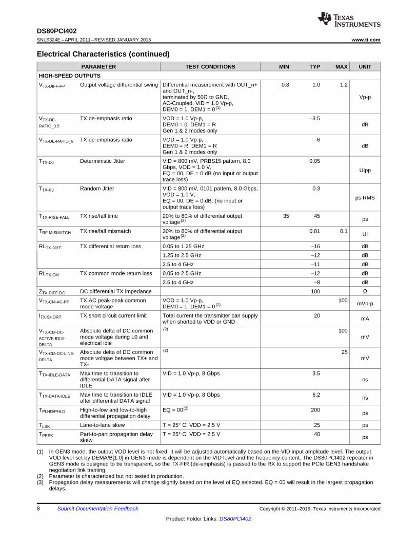
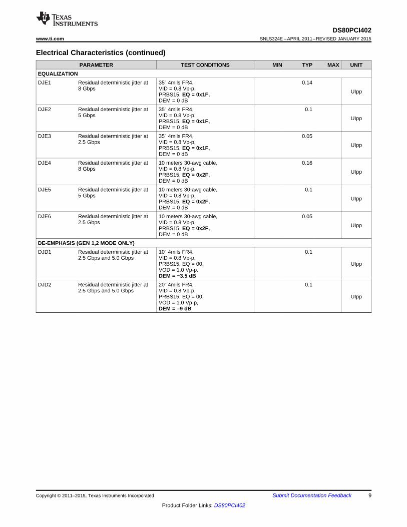
Electrical Characteristics (continued)PARAMETER TEST CONDITIONS MIN TYP MAX UNIT
HIGH-SPEED OUTPUTSVTX-DIFF-PP Output voltage differential swing Differential measurement with OUT_n+ 0.8 1.0 1.2
and OUT_n-,terminated by 50Ω to GND, Vp-pAC-Coupled, VID = 1.0 Vp-p,DEM0 = 1, DEM1 = 0 (1)
VTX-DE- TX de-emphasis ratio VOD = 1.0 Vp-p, –3.5RATIO_3.5 DEM0 = 0, DEM1 = R dB
Gen 1 & 2 modes onlyVTX-DE-RATIO_6 TX de-emphasis ratio VOD = 1.0 Vp-p, –6
DEM0 = R, DEM1 = R dBGen 1 & 2 modes only
TTX-DJ Deterministic Jitter VID = 800 mV, PRBS15 pattern, 8.0 0.05Gbps, VOD = 1.0 V, UIppEQ = 00, DE = 0 dB (no input or outputtrace loss)
TTX-RJ Random Jitter VID = 800 mV, 0101 pattern, 8.0 Gbps, 0.3VOD = 1.0 V, ps RMSEQ = 00, DE = 0 dB, (no input oroutput trace loss)
TTX-RISE-FALL TX rise/fall time 20% to 80% of differential output 35 45 psvoltage (2)
TRF-MISMATCH TX rise/fall mismatch 20% to 80% of differential output 0.01 0.1 UIvoltage (2)
RLTX-DIFF TX differential return loss 0.05 to 1.25 GHz –16 dB1.25 to 2.5 GHz –12 dB2.5 to 4 GHz –11 dB
RLTX-CM TX common mode return loss 0.05 to 2.5 GHz –12 dB2.5 to 4 GHz –8 dB
ZTX-DIFF-DC DC differential TX impedance 100 ΩVTX-CM-AC-PP TX AC peak-peak common VOD = 1.0 Vp-p, 100 mVp-pmode voltage DEM0 = 1, DEM1 = 0 (2)
ITX-SHORT TX short circuit current limit Total current the transmitter can supply 20 mAwhen shorted to VDD or GNDVTX-CM-DC- Absolute delta of DC common (2) 100ACTIVE-IDLE- mode voltage during L0 and mVDELTA electrical idleVTX-CM-DC-LINE- Absolute delta of DC common (2) 25DELTA mode voltgae between TX+ and mV
TX-TTX-IDLE-DATA Max time to transition to VID = 1.0 Vp-p, 8 Gbps 3.5
differential DATA signal after nsIDLE
TTX-DATA-IDLE Max time to transition to IDLE VID = 1.0 Vp-p, 8 Gbps 6.2 nsafter differential DATA signalTPLHD/PHLD High-to-low and low-to-high EQ = 00 (3) 200 psdifferential propagation delayTLSK Lane-to-lane skew T = 25° C, VDD = 2.5 V 25 psTPPSK Part-to-part propagation delay T = 25° C, VDD = 2.5 V 40 psskew
(1) In GEN3 mode, the output VOD level is not fixed. It will be adjusted automatically based on the VID input amplitude level. The outputVOD level set by DEMA/B[1:0] in GEN3 mode is dependent on the VID level and the frequency content. The DS80PCI402 repeater inGEN3 mode is designed to be transparent, so the TX-FIR (de-emphasis) is passed to the RX to support the PCIe GEN3 handshakenegotiation link training.
(2) Parameter is characterized but not tested in production.(3) Propagation delay measurements will change slightly based on the level of EQ selected. EQ = 00 will result in the largest propagation
delays.
8 Submit Documentation Feedback Copyright © 2011–2015, Texas Instruments Incorporated
Product Folder Links: DS80PCI402
DS80PCI402www.ti.com SNLS324E –APRIL 2011–REVISED JANUARY 2015
Electrical Characteristics (continued)PARAMETER TEST CONDITIONS MIN TYP MAX UNIT
EQUALIZATIONDJE1 Residual deterministic jitter at 35” 4mils FR4, 0.14
8 Gbps VID = 0.8 Vp-p, UIppPRBS15, EQ = 0x1F,DEM = 0 dB
DJE2 Residual deterministic jitter at 35” 4mils FR4, 0.15 Gbps VID = 0.8 Vp-p, UIppPRBS15, EQ = 0x1F,
DEM = 0 dBDJE3 Residual deterministic jitter at 35” 4mils FR4, 0.05
2.5 Gbps VID = 0.8 Vp-p, UIppPRBS15, EQ = 0x1F,DEM = 0 dB
DJE4 Residual deterministic jitter at 10 meters 30-awg cable, 0.168 Gbps VID = 0.8 Vp-p, UIppPRBS15, EQ = 0x2F,
DEM = 0 dBDJE5 Residual deterministic jitter at 10 meters 30-awg cable, 0.1
5 Gbps VID = 0.8 Vp-p, UIppPRBS15, EQ = 0x2F,DEM = 0 dB
DJE6 Residual deterministic jitter at 10 meters 30-awg cable, 0.052.5 Gbps VID = 0.8 Vp-p, UIppPRBS15, EQ = 0x2F,
DEM = 0 dBDE-EMPHASIS (GEN 1,2 MODE ONLY)DJD1 Residual deterministic jitter at 10” 4mils FR4, 0.1
2.5 Gbps and 5.0 Gbps VID = 0.8 Vp-p,PRBS15, EQ = 00, UIppVOD = 1.0 Vp-p,DEM = −3.5 dB
DJD2 Residual deterministic jitter at 20” 4mils FR4, 0.12.5 Gbps and 5.0 Gbps VID = 0.8 Vp-p,
PRBS15, EQ = 00, UIppVOD = 1.0 Vp-p,DEM = –9 dB
Copyright © 2011–2015, Texas Instruments Incorporated Submit Documentation Feedback 9
Product Folder Links: DS80PCI402

DS80PCI402SNLS324E –APRIL 2011–REVISED JANUARY 2015 www.ti.com
6.6 Electrical Characteristics — Serial Management Bus InterfaceOver recommended operating supply and temperature ranges unless other specified.
PARAMETER TEST CONDITIONS MIN TYP MAX UNITSERIAL BUS INTERFACE DC SPECIFICATIONSVIL Data, clock input low voltage 0.8 VVIH Data, clock input high voltage 2.1 3.6 VIPULLUP Current through pullup resistor or High Power Specification 4 mAcurrent sourceVDD Nominal bus voltage 2.375 3.6 VILEAK-Bus Input leakage per bus segment (1)-200 +200 µAILEAK-Pin Input leakage per device pin -15 µACI Capacitance for SDA and SCL (1) (2) 10 pFRTERM External termination resistance pull Pullup VDD = 3.3 V, 2000 Ωto VDD = 2.5 V ± 5% OR 3.3 V ± (1) (2) (3)
10% Pullup VDD = 2.5 V, 1000 Ω(1) (2) (3)
SERIAL BUS INTERFACE TIMING SPECIFICATIONSFSMB Bus operating frequency ENSMB = VDD (Slave Mode) 400 kHz
ENSMB = FLOAT (Master Mode) 280 400 520 kHzTBUF Bus free time between stop and 1.3 µsstart conditionTHD:STA Hold time after (repeated) start At IPULLUP, Max
condition. After this period, the first 0.6 µsclock is generated.
TSU:STA Repeated start condition setup time 0.6 µsTSU:STO Stop condition setup time 0.6 µsTHD:DAT Data hold time 0 nsTSU:DAT Data setup time 100 nsTLOW Clock low period 1.3 µsTHIGH Clock high period (4) 0.6 50 µstF Clock/data fall time (4) 300 nstR Clock/data rise time (4) 300 nstPOR Time in which a device must be (4) (5)
500 msoperational after power-on reset
(1) Recommended value.(2) Recommended maximum capacitance load per bus segment is 400 pF.(3) Maximum termination voltage should be identical to the device supply voltage.(4) Compliant to SMBus 2.0 physical layer specification. See System Management Bus (SMBus) Specification Version 2.0, section 3.1.1
SMBus common AC specifications for details.(5) Specified by Design. Parameter not tested in production.
10 Submit Documentation Feedback Copyright © 2011–2015, Texas Instruments Incorporated
Product Folder Links: DS80PCI402

1012
1014
1016
1018
1020
-40 -15 10 35 60 85
VO
D (
mV
p-p)
TEMPERATURE (°C)
VDD = 2.5 V
1007
1010
1013
1016
1019
1021
2.375 2.5 2.625
VO
D (
mV
p-p)
VDD (V)
T = 25°C
420.0
440.0
460.0
480.0
500.0
520.0
540.0
560.0
580.0
600.0
620.0
640.0
0.8 0.9 1 1.1 1.2 1.3
VOD (Vp-p)
PD
(m
W)
VDD = 2.625V
VDD = 2.5V
VDD = 2.375V
T = 25oC
DS80PCI402www.ti.com SNLS324E –APRIL 2011–REVISED JANUARY 2015
6.7 Typical Characteristics
Figure 1. Power Dissipation (PD) vs. Output Differential Figure 2. Output Differential Voltage (VOD = 1.0 Vp-p) vs.Voltage (VOD) Supply Voltage (VDD)
Figure 3. Output Differential Voltage (VOD = 1.0 Vp-p) vs. Temperature
Copyright © 2011–2015, Texas Instruments Incorporated Submit Documentation Feedback 11
Product Folder Links: DS80PCI402

SP
tBUFtHD:STA
tLOW
tR
tHD:DAT
tHIGH
tFtSU:DAT
tSU:STA
ST SP
tSU:STO
SCL
SDAST
IN
OUT
+
-tIDLE-DATA
+
-
tDATA-IDLE
DATA
IDLE
0V
0V
DATA
IDLE
IN 0V
tPLHD
OUT 0V
tPHLD
+
-
+
-
0V
20%
80%
20%
80%
tFALLtRISE
VOD = [Out+ - Out-]
DS80PCI402SNLS324E –APRIL 2011–REVISED JANUARY 2015 www.ti.com
7 Parameter Measurement Information
Figure 4. CML Output and Rise and Fall Transition Time
Figure 5. Propagation Delay Timing Diagram
Figure 6. Transmit Idle-Data and Data-Idle Response Time
Figure 7. SMBus Timing Parameters
12 Submit Documentation Feedback Copyright © 2011–2015, Texas Instruments Incorporated
Product Folder Links: DS80PCI402

One of Four B Channels
Digital Core and SMBus RegistersSCL
SDA
AD[3:0]
PRSNTInternal
3.3 V to 2.5 V Regulator
READ_EN
ALL_DONE
INA_[3:0]+
INA_[3:0]-EQ
OUTA_[3:0]+
OUTA_[3:0]-
One of Four A Channels
Term
Driver
RateDetect
SignalDetect
RATE
RXDET
VDD (x5)
ENSMB
EQA[1:0]
DEMA[1:0]
VIN
VDD_SEL
EQB[1:0]
DEMB[1:0]
INB_[3:0]+
INB_[3:0]-EQ Driver
OUTB_[3:0]+
OUTB_[3:0]-
RxDetect
Term
RateDetect
SignalDetect
RxDetect
Note: This diagram is representative of device signal flow only; Channels A and B are bi-directional channels.
DS80PCI402www.ti.com SNLS324E –APRIL 2011–REVISED JANUARY 2015
8 Detailed Description
8.1 OverviewThe DS80PCI402 provides input CTLE and output De-emphasis equalization for lossy printed circuit board traceand cables. The DS80PCI402 operates in three modes: Pin Control Mode configuration (ENSMB = 0), SMBusSlave Mode (ENSMB = 1) for register configurations from host controller or SMBus Master Mode (ENSMB =Float) for loading the register configurations from an external EEPROM.
8.2 Functional Block Diagram
Copyright © 2011–2015, Texas Instruments Incorporated Submit Documentation Feedback 13
Product Folder Links: DS80PCI402
DS80PCI402SNLS324E –APRIL 2011–REVISED JANUARY 2015 www.ti.com
8.3 Feature Description
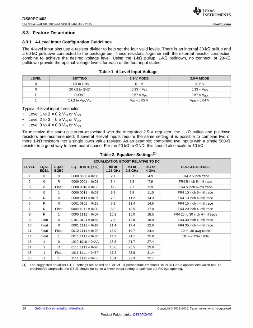
8.3.1 4-Level Input Configuration GuidelinesThe 4-level input pins use a resistor divider to help set the four valid levels. There is an internal 30-kΩ pullup anda 60-kΩ pulldown connected to the package pin. These resistors, together with the external resistor connectioncombine to achieve the desired voltage level. Using the 1-kΩ pullup, 1-kΩ pulldown, no connect, or 20-kΩpulldown provide the optimal voltage levels for each of the four input states.
Table 1. 4-Level Input VoltageLEVEL SETTING 3.3-V MODE 2.5-V MODE
0 1 kΩ to GND 0.1 V 0.08 VR 20 kΩ to GND 0.33 × VIN 0.33 × VDD
F FLOAT 0.67 × VIN 0.67 × VDD
1 1 kΩ to VDD/VIN VIN – 0.05 V VDD – 0.04 V
Typical 4-level input thresholds:• Level 1 to 2 = 0.2 VIN or VDD• Level 2 to 3 = 0.5 VIN or VDD• Level 3 to 4 = 0.8 VIN or VDD
To minimize the start-up current associated with the integrated 2.5-V regulator, the 1-kΩ pullup and pulldownresistors are recommended. If several 4-level inputs require the same setting, it is possible to combine two ormore 1-kΩ resistors into a single lower value resistor. As an example; combining two inputs with a single 500-Ωresistor is a good way to save board space. For the 20 kΩ to GND, this should also scale to 10 kΩ.
Table 2. Equalizer Settings (1)
EQUALIZATION BOOST RELATIVE TO DCLEVEL EQA1 EQA0 EQ – 8 BITS [7:0] dB at dB at dB at SUGGESTED USE
EQB1 EQB0 1.25 GHz 2.5 GHz 4 GHz1 0 0 0000 0000 = 0x00 2.1 3.7 4.9 FR4 < 5 inch trace2 0 R 0000 0001 = 0x01 3.4 5.8 7.9 FR4 5 inch 5–mil trace3 0 Float 0000 0010 = 0x02 4.8 7.7 9.9 FR4 5 inch 4–mil trace4 0 1 0000 0011 = 0x03 5.9 8.9 11.0 FR4 10 inch 5–mil trace5 R 0 0000 0111 = 0x07 7.2 11.2 14.3 FR4 10 inch 4–mil trace6 R R 0001 0101 = 0x15 6.1 11.4 14.6 FR4 15 inch 4–mil trace7 R Float 0000 1011 = 0x0B 8.8 13.5 17.0 FR4 20 inch 4–mil trace8 R 1 0000 1111 = 0x0F 10.2 15.0 18.5 FR4 25 to 30 inch 4–mil trace9 Float 0 0101 0101 = 0x55 7.5 12.8 18.0 FR4 30 inch 4–mil trace
10 Float R 0001 1111 = 0x1F 11.4 17.4 22.0 FR4 35 inch 4–mil trace11 Float Float 0010 1111 = 0x2F 13.0 19.7 24.4 10 m, 30-awg cable12 Float 1 0011 1111 = 0x3F 14.2 21.1 25.8 10 m – 12m cable13 1 0 1010 1010 = 0xAA 13.8 21.7 27.414 1 R 0111 1111 = 0x7F 15.6 23.5 29.015 1 Float 1011 1111 = 0xBF 17.2 25.8 31.416 1 1 1111 1111 = 0xFF 18.4 27.3 32.7
(1) The suggested equalizer CTLE settings are based on 0 dB of TX preshoot/de-emphasis. In PCIe Gen 3 applications which use TXpreshoot/de-emphasis, the CTLE should be set to a lower boost setting to optimize the RX eye opening.
14 Submit Documentation Feedback Copyright © 2011–2015, Texas Instruments Incorporated
Product Folder Links: DS80PCI402

DS80PCI402www.ti.com SNLS324E –APRIL 2011–REVISED JANUARY 2015
Table 3. Output Voltage and De-Emphasis Settings (1)
LEVEL DEMA1 DEMA0 VOD Vp-p DEM dB INNER AMPLITUDE SUGGESTED USEDEMB1 DEMB0 (see (1)) Vp-p
1 0 0 0.8 0 0.8 FR4 < 5 inch 4-mil trace2 0 R 0.9 0 0.9 FR4 < 5 inch 4-mil trace3 0 Float 0.9 –3.5 0.6 FR4 10 inch 4-mil trace4 0 1 1.0 0 1.0 FR4 < 5 inch 4-mil trace5 R 0 1.0 –3.5 0.7 FR4 10 inch 4-mil trace6 R R 1.0 –6 0.5 FR4 15 inch 4-mil trace7 R Float 1.1 0 1.1 FR4 < 5 inch 4-mil trace8 R 1 1.1 –3.5 0.7 FR4 10 inch 4-mil trace9 Float 0 1.1 –6 0.6 FR4 15 inch 4-mil trace10 Float R 1.2 0 1.2 FR4 < 5 inch 4-mil trace11 Float Float 1.2 –3.5 0.8 FR4 10 inch 4-mil trace12 Float 1 1.2 –6 0.6 FR4 15 inch 4-mil trace13 1 0 1.3 0 1.3 FR4 < 5 inch 4-mil trace14 1 R 1.3 –3.5 0.9 FR4 10 inch 4-mil trace15 1 Float 1.3 –6 0.7 FR4 15 inch 4-mil trace16 1 1 1.3 –9 0.5 FR4 20 inch 4-mil trace
(1) The VOD output amplitude and DEM de-emphasis levels are set with the DEMA/B[1:0] pins.The de-emphasis levels are available in GEN1, GEN2, and GEN 3 modes when RATE = Float.
Table 4. RX-Detect SettingsPRSNT (1) RXDET SMBus REG INPUT TERMINATION COMMENTS(PIN 52) (PIN 22) BIT[3:2]
0 0 00 Hi-Z Manual RX-Detect, input is high-impedance mode0 Tie 20 kΩ 01 Pre Detect: Hi-Z Auto RX-Detect, outputs test every 12 ms for 600 ms
to GND Post Detect: 50 Ω then stops; termination is hi-Z until detection; oncedetected input termination is 50 ΩReset function by pulsing PRSNT high for 5 µs thenlow again
0 Float 10 Pre Detect: Hi-Z Auto RX-Detect, outputs test every 12 ms until(Default) Post Detect: 50 Ω detection occurs; termination is hi-Z until detection;
once detected input termination is 50 ΩReset function by pulsing PRSNT high for 5 µs thenlow again
0 1 11 50 Ω Manual RX-Detect, input is 50 Ω1 X Hi-Z Power-down mode, input is high impedance, output
drivers are disabledUsed to reset RX-Detect State Machine when heldhigh for 5 µs
(1) In SMBus Slave Mode, the Rx Detect State Machine can be manually reset in software by overriding the device PRSNT function. This isaccomplished by setting the Override RXDET bit (Reg 0x02[7]) and then toggling the RXDET Value bit (Reg 0x02[6]). See Table 9 formore information about resetting the Rx Detect State Machine.
Copyright © 2011–2015, Texas Instruments Incorporated Submit Documentation Feedback 15
Product Folder Links: DS80PCI402
DS80PCI402SNLS324E –APRIL 2011–REVISED JANUARY 2015 www.ti.com
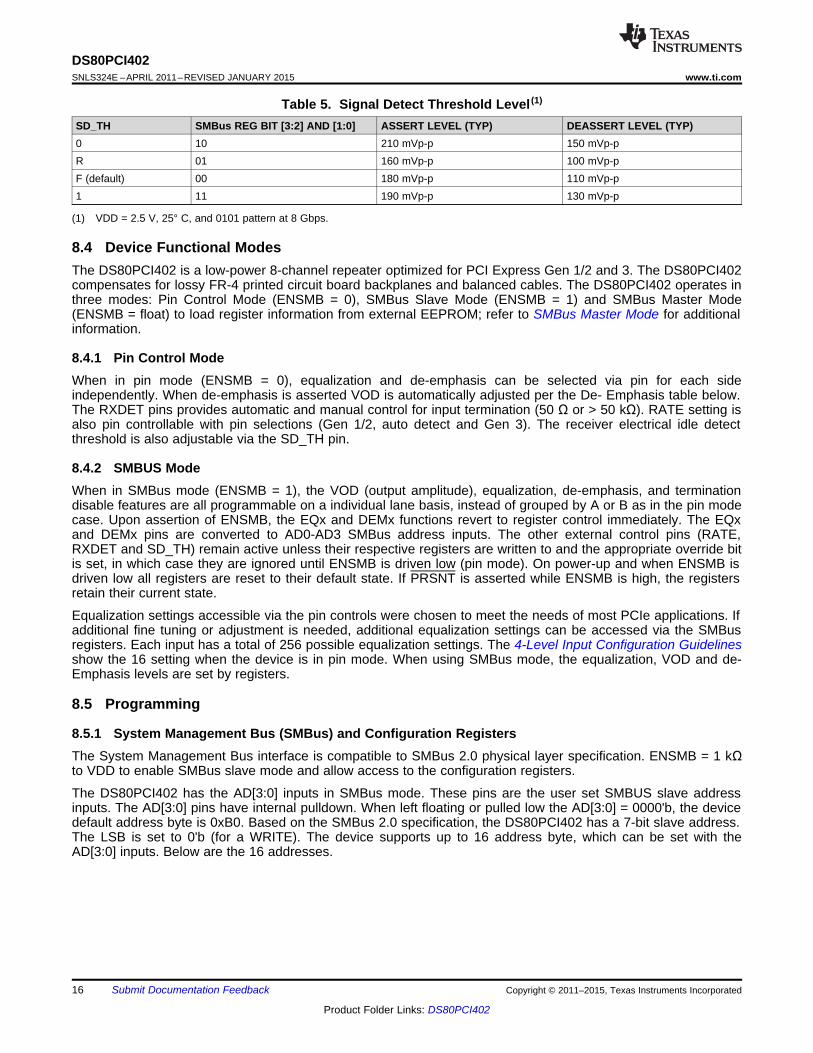
Table 5. Signal Detect Threshold Level (1)
SD_TH SMBus REG BIT [3:2] AND [1:0] ASSERT LEVEL (TYP) DEASSERT LEVEL (TYP)0 10 210 mVp-p 150 mVp-pR 01 160 mVp-p 100 mVp-pF (default) 00 180 mVp-p 110 mVp-p1 11 190 mVp-p 130 mVp-p
(1) VDD = 2.5 V, 25° C, and 0101 pattern at 8 Gbps.
8.4 Device Functional ModesThe DS80PCI402 is a low-power 8-channel repeater optimized for PCI Express Gen 1/2 and 3. The DS80PCI402compensates for lossy FR-4 printed circuit board backplanes and balanced cables. The DS80PCI402 operates inthree modes: Pin Control Mode (ENSMB = 0), SMBus Slave Mode (ENSMB = 1) and SMBus Master Mode(ENSMB = float) to load register information from external EEPROM; refer to SMBus Master Mode for additionalinformation.
8.4.1 Pin Control ModeWhen in pin mode (ENSMB = 0), equalization and de-emphasis can be selected via pin for each sideindependently. When de-emphasis is asserted VOD is automatically adjusted per the De- Emphasis table below.The RXDET pins provides automatic and manual control for input termination (50 Ω or > 50 kΩ). RATE setting isalso pin controllable with pin selections (Gen 1/2, auto detect and Gen 3). The receiver electrical idle detectthreshold is also adjustable via the SD_TH pin.
8.4.2 SMBUS ModeWhen in SMBus mode (ENSMB = 1), the VOD (output amplitude), equalization, de-emphasis, and terminationdisable features are all programmable on a individual lane basis, instead of grouped by A or B as in the pin modecase. Upon assertion of ENSMB, the EQx and DEMx functions revert to register control immediately. The EQxand DEMx pins are converted to AD0-AD3 SMBus address inputs. The other external control pins (RATE,RXDET and SD_TH) remain active unless their respective registers are written to and the appropriate override bitis set, in which case they are ignored until ENSMB is driven low (pin mode). On power-up and when ENSMB isdriven low all registers are reset to their default state. If PRSNT is asserted while ENSMB is high, the registersretain their current state.
Equalization settings accessible via the pin controls were chosen to meet the needs of most PCIe applications. Ifadditional fine tuning or adjustment is needed, additional equalization settings can be accessed via the SMBusregisters. Each input has a total of 256 possible equalization settings. The 4-Level Input Configuration Guidelinesshow the 16 setting when the device is in pin mode. When using SMBus mode, the equalization, VOD and de-Emphasis levels are set by registers.
8.5 Programming
8.5.1 System Management Bus (SMBus) and Configuration RegistersThe System Management Bus interface is compatible to SMBus 2.0 physical layer specification. ENSMB = 1 kΩto VDD to enable SMBus slave mode and allow access to the configuration registers.
The DS80PCI402 has the AD[3:0] inputs in SMBus mode. These pins are the user set SMBUS slave addressinputs. The AD[3:0] pins have internal pulldown. When left floating or pulled low the AD[3:0] = 0000'b, the devicedefault address byte is 0xB0. Based on the SMBus 2.0 specification, the DS80PCI402 has a 7-bit slave address.The LSB is set to 0'b (for a WRITE). The device supports up to 16 address byte, which can be set with theAD[3:0] inputs. Below are the 16 addresses.
16 Submit Documentation Feedback Copyright © 2011–2015, Texas Instruments Incorporated
Product Folder Links: DS80PCI402

DS80PCI402www.ti.com SNLS324E –APRIL 2011–REVISED JANUARY 2015
Programming (continued)Table 6. Device Slave Address Bytes
AD[3:0] SETTINGS ADDRESS BYTES (HEX) 7-BIT SLAVE ADDRESS (HEX)0000 B0 580001 B2 590010 B4 5A0011 B6 5B0100 B8 5C0101 BA 5D0110 BC 5E0111 BE 5F1000 C0 601001 C2 611010 C4 621011 C6 631100 C8 641101 CA 651110 CC 661111 CE 67
The SDA/SCL pins are 3.3 V tolerant, but are not 5 V tolerant. An external pullup resistor is required on the SDAand SCL line. The resistor value can be from 2 kΩ to 5 kΩ depending on the voltage, loading, and speed.
8.5.2 Transfer of Data Through the SMBusDuring normal operation the data on SDA must be stable during the time when SCL is High.
There are three unique states for the SMBus:
START: A high-to-low transition on SDA while SCL is High indicates a message START condition.
STOP: A low-to-high transition on SDA while SCL is High indicates a message STOP condition.
IDLE: If SCL and SDA are both High for a time exceeding tBUF from the last detected STOP condition or if theyare High for a total exceeding the maximum specification for tHIGH then the bus will transfer to the IDLE state.
8.5.3 Writing a RegisterTo write a register, the following protocol is used (see SMBus 2.0 specification).1. The Host drives a START condition, the 7-bit SMBus address, and a “0” indicating a WRITE.2. The Device (Slave) drives the ACK bit (“0”).3. The Host drives the 8-bit Register Address.4. The Device drives an ACK bit (“0”).5. The Host drive the 8-bit data byte.6. The Device drives an ACK bit (“0”).7. The Host drives a STOP condition.
The WRITE transaction is completed, the bus goes IDLE and communication with other SMBus devices maynow occur.
Copyright © 2011–2015, Texas Instruments Incorporated Submit Documentation Feedback 17
Product Folder Links: DS80PCI402

DS80PCI402SNLS324E –APRIL 2011–REVISED JANUARY 2015 www.ti.com
8.5.4 Reading a RegisterTo read a register, the following protocol is used (see SMBus 2.0 specification).1. The Host drives a START condition, the 7-bit SMBus address, and a “0” indicating a WRITE.2. The Device (Slave) drives the ACK bit (“0”).3. The Host drives the 8-bit Register Address.4. The Device drives an ACK bit (“0”).5. The Host drives a START condition.6. The Host drives the 7-bit SMBus Address, and a “1” indicating a READ.7. The Device drives an ACK bit “0”.8. The Device drives the 8-bit data value (register contents).9. The Host drives a NACK bit “1”indicating end of the READ transfer.10. The Host drives a STOP condition.
The READ transaction is completed, the bus goes IDLE and communication with other SMBus devices may nowoccur.
8.5.5 SMBus Master ModeThe DS80PCI402 device supports reading directly from an external EEPROM device by implementing SMBusMaster mode. When using the SMBus master mode, the DS80PCI402 will read directly from specific location inthe external EEPROM. When designing a system for using the external EEPROM, the user needs to follow thesespecific guidelines.• Set ENSMB = Float — enable the SMBUS master mode.• The external EEPROM device address byte must be 0xA0 and capable of 1-MHz operation at 2.5-V and 3.3-
V supply. The maximum allowed size is 8 kbits (1024 bytes)• Set the AD[3:0] inputs for SMBus address byte. When the AD[3:0] = 0000'b, the device address byte is 0xB0.
When tying multiple DS80PCI402 devices to the SDA and SCL bus, use these guidelines to configure thedevices.• Use SMBus AD[3:0] address bits so that each device can loaded its configuration from the EEPROM.
Example below is for 4 devices.– U1: AD[3:0] = 0000 = 0xB0– U2: AD[3:0] = 0001 = 0xB2– U3: AD[3:0] = 0010 = 0xB4– U4: AD[3:0] = 0011 = 0xB6
• Use a pullup resistor on SDA and SCL; value = 2 kΩ• Daisy-chain READ_EN (pin 26) and ALL_DONE (pin 27) from one device to the next device in the sequence
so that they do not compete for the EEPROM at the same time.1. Tie READ_EN of the first device in the chain (U1) to GND2. Tie ALL_DONE of U1 to READ_EN of U23. Tie ALL_DONE of U2 to READ_EN of U34. Tie ALL_DONE of U3 to READ_EN of U45. Optional: Tie ALL_DONE output of U4 to a LED to show the devices have been loaded successfully
18 Submit Documentation Feedback Copyright © 2011–2015, Texas Instruments Incorporated
Product Folder Links: DS80PCI402
DS80PCI402www.ti.com SNLS324E –APRIL 2011–REVISED JANUARY 2015
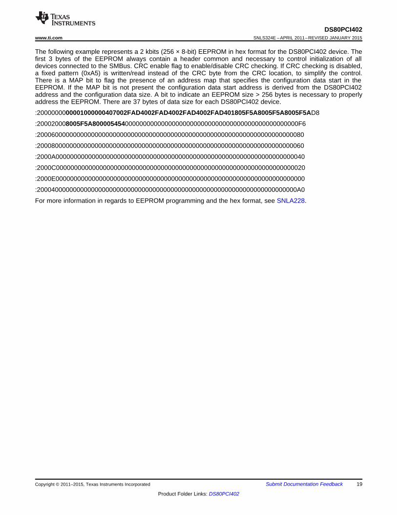
The following example represents a 2 kbits (256 × 8-bit) EEPROM in hex format for the DS80PCI402 device. Thefirst 3 bytes of the EEPROM always contain a header common and necessary to control initialization of alldevices connected to the SMBus. CRC enable flag to enable/disable CRC checking. If CRC checking is disabled,a fixed pattern (0xA5) is written/read instead of the CRC byte from the CRC location, to simplify the control.There is a MAP bit to flag the presence of an address map that specifies the configuration data start in theEEPROM. If the MAP bit is not present the configuration data start address is derived from the DS80PCI402address and the configuration data size. A bit to indicate an EEPROM size > 256 bytes is necessary to properlyaddress the EEPROM. There are 37 bytes of data size for each DS80PCI402 device.
:2000000000001000000407002FAD4002FAD4002FAD4002FAD401805F5A8005F5A8005F5AD8
:200020008005F5A800005454000000000000000000000000000000000000000000000000F6
:20006000000000000000000000000000000000000000000000000000000000000000000080
:20008000000000000000000000000000000000000000000000000000000000000000000060
:2000A000000000000000000000000000000000000000000000000000000000000000000040
:2000C000000000000000000000000000000000000000000000000000000000000000000020
:2000E000000000000000000000000000000000000000000000000000000000000000000000
:200040000000000000000000000000000000000000000000000000000000000000000000A0
For more information in regards to EEPROM programming and the hex format, see SNLA228.
Copyright © 2011–2015, Texas Instruments Incorporated Submit Documentation Feedback 19
Product Folder Links: DS80PCI402
DS80PCI402SNLS324E –APRIL 2011–REVISED JANUARY 2015 www.ti.com
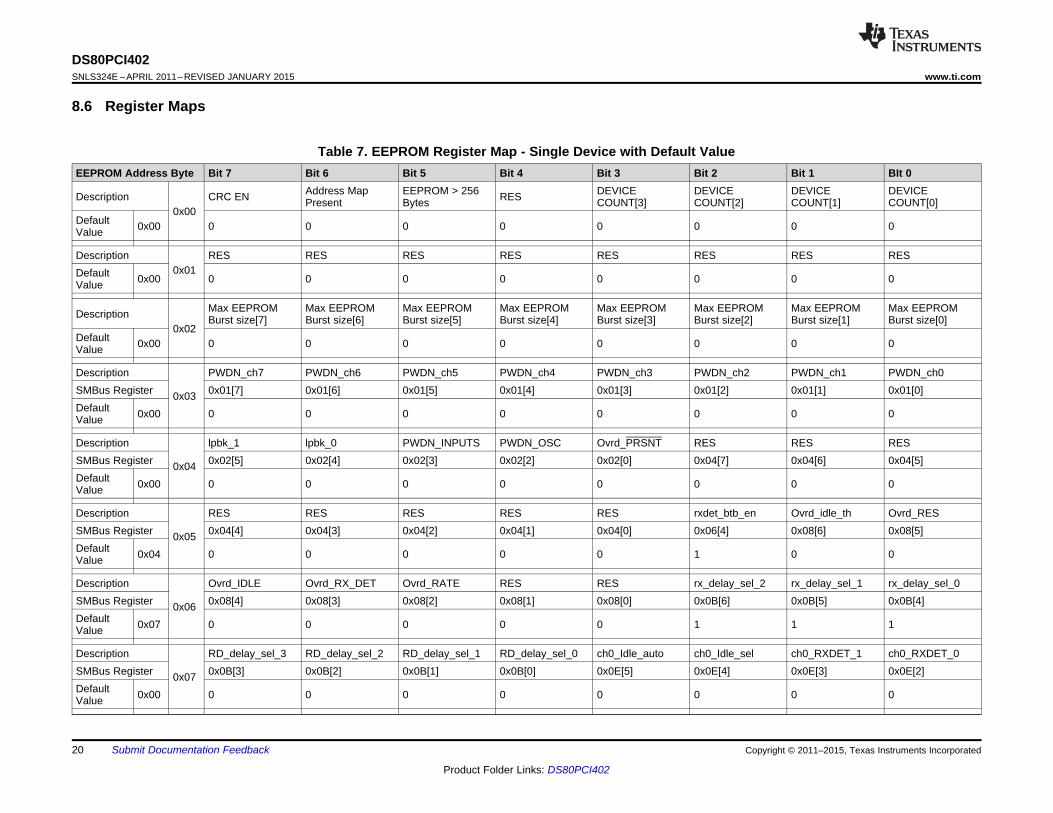
8.6 Register Maps
Table 7. EEPROM Register Map - Single Device with Default ValueEEPROM Address Byte Bit 7 Bit 6 Bit 5 Bit 4 Bit 3 Bit 2 Bit 1 BIt 0
Address Map EEPROM > 256 DEVICE DEVICE DEVICE DEVICEDescription CRC EN RESPresent Bytes COUNT[3] COUNT[2] COUNT[1] COUNT[0]0x00
Default 0x00 0 0 0 0 0 0 0 0Value
Description RES RES RES RES RES RES RES RES0x01Default 0x00 0 0 0 0 0 0 0 0Value
Max EEPROM Max EEPROM Max EEPROM Max EEPROM Max EEPROM Max EEPROM Max EEPROM Max EEPROMDescription Burst size[7] Burst size[6] Burst size[5] Burst size[4] Burst size[3] Burst size[2] Burst size[1] Burst size[0]0x02
Default 0x00 0 0 0 0 0 0 0 0Value
Description PWDN_ch7 PWDN_ch6 PWDN_ch5 PWDN_ch4 PWDN_ch3 PWDN_ch2 PWDN_ch1 PWDN_ch0SMBus Register 0x01[7] 0x01[6] 0x01[5] 0x01[4] 0x01[3] 0x01[2] 0x01[1] 0x01[0]0x03Default 0x00 0 0 0 0 0 0 0 0Value
Description lpbk_1 lpbk_0 PWDN_INPUTS PWDN_OSC Ovrd_PRSNT RES RES RESSMBus Register 0x02[5] 0x02[4] 0x02[3] 0x02[2] 0x02[0] 0x04[7] 0x04[6] 0x04[5]0x04Default 0x00 0 0 0 0 0 0 0 0Value
Description RES RES RES RES RES rxdet_btb_en Ovrd_idle_th Ovrd_RESSMBus Register 0x04[4] 0x04[3] 0x04[2] 0x04[1] 0x04[0] 0x06[4] 0x08[6] 0x08[5]0x05Default 0x04 0 0 0 0 0 1 0 0Value
Description Ovrd_IDLE Ovrd_RX_DET Ovrd_RATE RES RES rx_delay_sel_2 rx_delay_sel_1 rx_delay_sel_0SMBus Register 0x08[4] 0x08[3] 0x08[2] 0x08[1] 0x08[0] 0x0B[6] 0x0B[5] 0x0B[4]0x06Default 0x07 0 0 0 0 0 1 1 1Value
Description RD_delay_sel_3 RD_delay_sel_2 RD_delay_sel_1 RD_delay_sel_0 ch0_Idle_auto ch0_Idle_sel ch0_RXDET_1 ch0_RXDET_0SMBus Register 0x0B[3] 0x0B[2] 0x0B[1] 0x0B[0] 0x0E[5] 0x0E[4] 0x0E[3] 0x0E[2]0x07Default 0x00 0 0 0 0 0 0 0 0Value
20 Submit Documentation Feedback Copyright © 2011–2015, Texas Instruments Incorporated
Product Folder Links: DS80PCI402
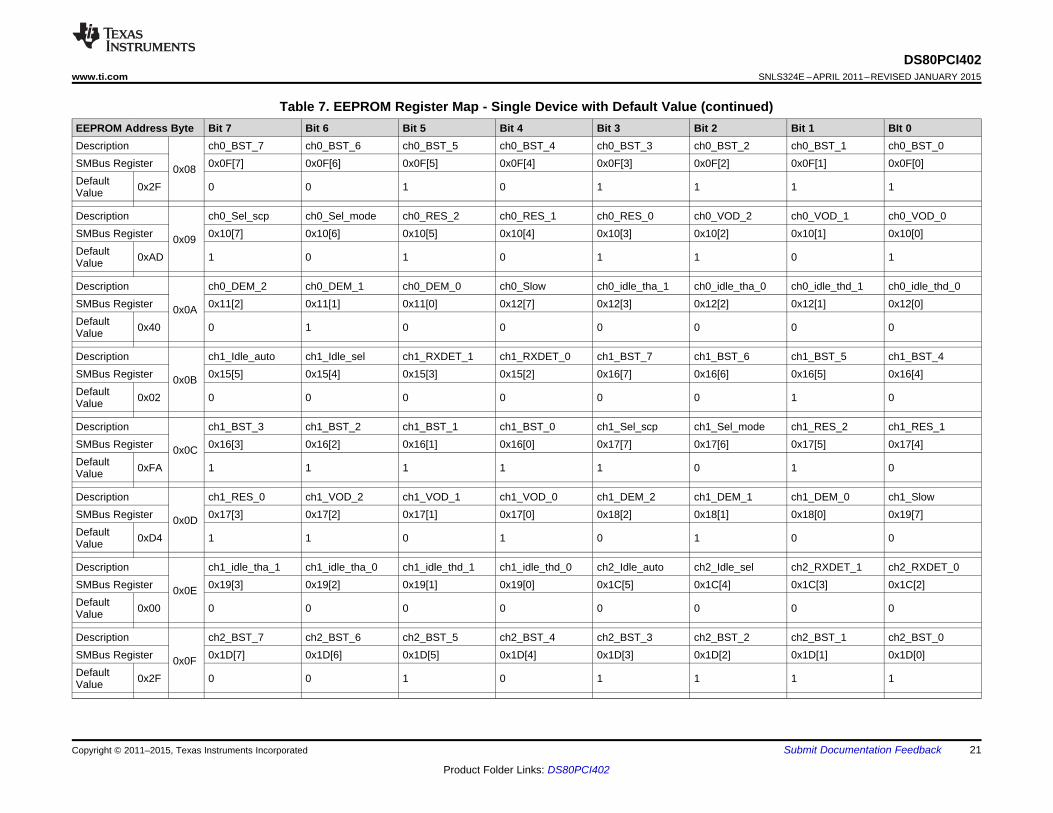
DS80PCI402www.ti.com SNLS324E –APRIL 2011–REVISED JANUARY 2015
Table 7. EEPROM Register Map - Single Device with Default Value (continued)EEPROM Address Byte Bit 7 Bit 6 Bit 5 Bit 4 Bit 3 Bit 2 Bit 1 BIt 0Description ch0_BST_7 ch0_BST_6 ch0_BST_5 ch0_BST_4 ch0_BST_3 ch0_BST_2 ch0_BST_1 ch0_BST_0SMBus Register 0x0F[7] 0x0F[6] 0x0F[5] 0x0F[4] 0x0F[3] 0x0F[2] 0x0F[1] 0x0F[0]0x08Default 0x2F 0 0 1 0 1 1 1 1Value
Description ch0_Sel_scp ch0_Sel_mode ch0_RES_2 ch0_RES_1 ch0_RES_0 ch0_VOD_2 ch0_VOD_1 ch0_VOD_0SMBus Register 0x10[7] 0x10[6] 0x10[5] 0x10[4] 0x10[3] 0x10[2] 0x10[1] 0x10[0]0x09Default 0xAD 1 0 1 0 1 1 0 1Value
Description ch0_DEM_2 ch0_DEM_1 ch0_DEM_0 ch0_Slow ch0_idle_tha_1 ch0_idle_tha_0 ch0_idle_thd_1 ch0_idle_thd_0SMBus Register 0x11[2] 0x11[1] 0x11[0] 0x12[7] 0x12[3] 0x12[2] 0x12[1] 0x12[0]0x0ADefault 0x40 0 1 0 0 0 0 0 0Value
Description ch1_Idle_auto ch1_Idle_sel ch1_RXDET_1 ch1_RXDET_0 ch1_BST_7 ch1_BST_6 ch1_BST_5 ch1_BST_4SMBus Register 0x15[5] 0x15[4] 0x15[3] 0x15[2] 0x16[7] 0x16[6] 0x16[5] 0x16[4]0x0BDefault 0x02 0 0 0 0 0 0 1 0Value
Description ch1_BST_3 ch1_BST_2 ch1_BST_1 ch1_BST_0 ch1_Sel_scp ch1_Sel_mode ch1_RES_2 ch1_RES_1SMBus Register 0x16[3] 0x16[2] 0x16[1] 0x16[0] 0x17[7] 0x17[6] 0x17[5] 0x17[4]0x0CDefault 0xFA 1 1 1 1 1 0 1 0Value
Description ch1_RES_0 ch1_VOD_2 ch1_VOD_1 ch1_VOD_0 ch1_DEM_2 ch1_DEM_1 ch1_DEM_0 ch1_SlowSMBus Register 0x17[3] 0x17[2] 0x17[1] 0x17[0] 0x18[2] 0x18[1] 0x18[0] 0x19[7]0x0DDefault 0xD4 1 1 0 1 0 1 0 0Value
Description ch1_idle_tha_1 ch1_idle_tha_0 ch1_idle_thd_1 ch1_idle_thd_0 ch2_Idle_auto ch2_Idle_sel ch2_RXDET_1 ch2_RXDET_0SMBus Register 0x19[3] 0x19[2] 0x19[1] 0x19[0] 0x1C[5] 0x1C[4] 0x1C[3] 0x1C[2]0x0EDefault 0x00 0 0 0 0 0 0 0 0Value
Description ch2_BST_7 ch2_BST_6 ch2_BST_5 ch2_BST_4 ch2_BST_3 ch2_BST_2 ch2_BST_1 ch2_BST_0SMBus Register 0x1D[7] 0x1D[6] 0x1D[5] 0x1D[4] 0x1D[3] 0x1D[2] 0x1D[1] 0x1D[0]0x0FDefault 0x2F 0 0 1 0 1 1 1 1Value
Copyright © 2011–2015, Texas Instruments Incorporated Submit Documentation Feedback 21
Product Folder Links: DS80PCI402

DS80PCI402SNLS324E –APRIL 2011–REVISED JANUARY 2015 www.ti.com
Table 7. EEPROM Register Map - Single Device with Default Value (continued)EEPROM Address Byte Bit 7 Bit 6 Bit 5 Bit 4 Bit 3 Bit 2 Bit 1 BIt 0Description ch2_Sel_scp ch2_Sel_mode ch2_RES_2 ch2_RES_1 ch2_RES_0 ch2_VOD_2 ch2_VOD_1 ch2_VOD_0SMBus Register 0x1E[7] 0x1E[6] 0x1E[5] 0x1E[4] 0x1E[3] 0x1E[2] 0x1E[1] 0x1E[0]0x10Default 0xAD 1 0 1 0 1 1 0 1Value
Description ch2_DEM_2 ch2_DEM_1 ch2_DEM_0 ch2_Slow ch2_idle_tha_1 ch2_idle_tha_0 ch2_idle_thd_1 ch2_idle_thd_0SMBus Register 0x1F[2] 0x1F[1] 0x1F[0] 0x20[7] 0x20[3] 0x20[2] 0x20[1] 0x20[0]0x11Default 0x40 0 1 0 0 0 0 0 0Value
Description ch3_Idle_auto ch3_Idle_sel ch3_RXDET_1 ch3_RXDET_0 ch3_BST_7 ch3_BST_6 ch3_BST_5 ch3_BST_4SMBus Register 0x23[5] 0x23[4] 0x23[3] 0x23[2] 0x24[7] 0x24[6] 0x24[5] 0x24[4]0x12Default 0x02 0 0 0 0 0 0 1 0Value
Description ch3_BST_3 ch3_BST_2 ch3_BST_1 ch3_BST_0 ch3_Sel_scp ch3_Sel_mode ch3_RES_2 ch3_RES_1SMBus Register 0x24[3] 0x24[2] 0x24[1] 0x24[0] 0x25[7] 0x25[6] 0x25[5] 0x25[4]0x13Default 0xFA 1 1 1 1 1 0 1 0Value
Description ch3_RES_0 ch3_VOD_2 ch3_VOD_1 ch3_VOD_0 ch3_DEM_2 ch3_DEM_1 ch3_DEM_0 ch3_SlowSMBus Register 0x25[3] 0x25[2] 0x25[1] 0x25[0] 0x26[2] 0x26[1] 0x26[0] 0x27[7]0x14Default 0xD4 1 1 0 1 0 1 0 0Value
Description ch3_idle_tha_1 ch3_idle_tha_0 ch3_idle_thd_1 ch3_idle_thd_0 ovrd_fast_idle en_high_idle_th_n en_high_idle_th_s en_fast_idle_nSMBus Register 0x27[3] 0x27[2] 0x27[1] 0x27[0] 0x28[6] 0x28[5] 0x28[4] 0x28[3]0x15Default 0x09 0 0 0 0 0 0 0 1Value
Description en_fast_idle_s eqsd_mgain_n eqsd_mgain_s ch4_Idle_auto ch4_Idle_sel ch4_RXDET_1 ch4_RXDET_0 ch4_BST_7SMBus Register 0x28[2] 0x28[1] 0x28[0] 0x2B[5] 0x2B[4] 0x2B[3] 0x2B[2] 0x2C[7]0x16Default 0x80 1 0 0 0 0 0 0 0Value
Description ch4_BST_6 ch4_BST_5 ch4_BST_4 ch4_BST_3 ch4_BST_2 ch4_BST_1 ch4_BST_0 ch4_Sel_scpSMBus Register 0x2C[6] 0x2C[5] 0x2C[4] 0x2C[3] 0x2C[2] 0x2C[1] 0x2C[0] 0x2D[7]0x17Default 0x5F 0 1 0 1 1 1 1 1Value
22 Submit Documentation Feedback Copyright © 2011–2015, Texas Instruments Incorporated
Product Folder Links: DS80PCI402

DS80PCI402www.ti.com SNLS324E –APRIL 2011–REVISED JANUARY 2015
Table 7. EEPROM Register Map - Single Device with Default Value (continued)EEPROM Address Byte Bit 7 Bit 6 Bit 5 Bit 4 Bit 3 Bit 2 Bit 1 BIt 0Description ch4_Sel_mode ch4_RES_2 ch4_RES_1 ch4_RES_0 ch4_VOD_2 ch4_VOD_1 ch4_VOD_0 ch4_DEM_2SMBus Register 0x2D[6] 0x2D[5] 0x2D[4] 0x2D[3] 0x2D[2] 0x2D[1] 0x2D[0] 0x2E[2]0x18Default 0x5A 0 1 0 1 1 0 1 0Value
Description ch4_DEM_1 ch4_DEM_0 ch4_Slow ch4_idle_tha_1 ch4_idle_tha_0 ch4_idle_thd_1 ch4_idle_thd_0 ch5_Idle_autoSMBus Register 0x2E[1] 0x2E[0] 0x2F[7] 0x2F[3] 0x2F[2] 0x2F[1] 0x2F[0] 0x32[5]0x19Default 0x80 1 0 0 0 0 0 0 0Value
Description ch5_Idle_sel ch5_RXDET_1 ch5_RXDET_0 ch5_BST_7 ch5_BST_6 ch5_BST_5 ch5_BST_4 ch5_BST_3SMBus Register 0x32[4] 0x32[3] 0x32[2] 0x33[7] 0x33[6] 0x33[5] 0x33[4] 0x33[3]0x1ADefault 0x05 0 0 0 0 0 1 0 1Value
Description ch5_BST_2 ch5_BST_1 ch5_BST_0 ch5_Sel_scp ch5_Sel_mode ch5_RES_2 ch5_RES_1 ch5_RES_0SMBus Register 0x33[2] 0x33[1] 0x33[0] 0x34[7] 0x34[6] 0x34[5] 0x34[4] 0x34[3]0x1BDefault 0xF5 1 1 1 1 0 1 0 1Value
Description ch5_VOD_2 ch5_VOD_1 ch5_VOD_0 ch5_DEM_2 ch5_DEM_1 ch5_DEM_0 ch5_Slow ch5_idle_tha_1SMBus Register 0x34[2] 0x34[1] 0x34[0] 0x35[2] 0x35[1] 0x35[0] 0x36[7] 0x36[3]0x1CDefault 0xA8 1 0 1 0 1 0 0 0Value
Description ch5_idle_tha_0 ch5_idle_thd_1 ch5_idle_thd_0 ch6_Idle_auto ch6_Idle_sel ch6_RXDET_1 ch6_RXDET_0 ch6_BST_7SMBus Register 0x36[2] 0x36[1] 0x36[0] 0x39[5] 0x39[4] 0x39[3] 0x39[2] 0x3A[7]0x1DDefault 0x00 0 0 0 0 0 0 0 0Value
Description ch6_BST_6 ch6_BST_5 ch6_BST_4 ch6_BST_3 ch6_BST_2 ch6_BST_1 ch6_BST_0 ch6_Sel_scpSMBus Register 0x3A[6] 0x3A[5] 0x3A[4] 0x3A[3] 0x3A[2] 0x3A[1] 0x3A[0] 0x3B[7]0x1EDefault 0x5F 0 1 0 1 1 1 1 1Value
Description ch6_Sel_mode ch6_RES_2 ch6_RES_1 ch6_RES_0 ch6_VOD_2 ch6_VOD_1 ch6_VOD_0 ch6_DEM_2SMBus Register 0x3B[6] 0x3B[5] 0x3B[4] 0x3B[3] 0x3B[2] 0x3B[1] 0x3B[0] 0x3C[2]0x1FDefault 0x5A 0 1 0 1 1 0 1 0Value
Copyright © 2011–2015, Texas Instruments Incorporated Submit Documentation Feedback 23
Product Folder Links: DS80PCI402
DS80PCI402SNLS324E –APRIL 2011–REVISED JANUARY 2015 www.ti.com
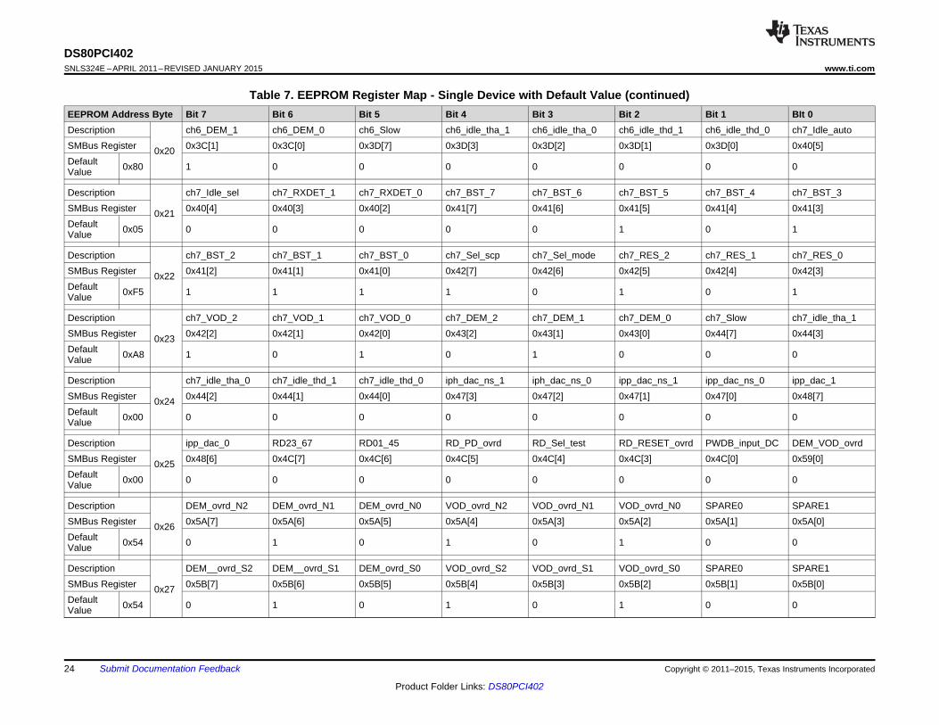
Table 7. EEPROM Register Map - Single Device with Default Value (continued)EEPROM Address Byte Bit 7 Bit 6 Bit 5 Bit 4 Bit 3 Bit 2 Bit 1 BIt 0Description ch6_DEM_1 ch6_DEM_0 ch6_Slow ch6_idle_tha_1 ch6_idle_tha_0 ch6_idle_thd_1 ch6_idle_thd_0 ch7_Idle_autoSMBus Register 0x3C[1] 0x3C[0] 0x3D[7] 0x3D[3] 0x3D[2] 0x3D[1] 0x3D[0] 0x40[5]0x20Default 0x80 1 0 0 0 0 0 0 0Value
Description ch7_Idle_sel ch7_RXDET_1 ch7_RXDET_0 ch7_BST_7 ch7_BST_6 ch7_BST_5 ch7_BST_4 ch7_BST_3SMBus Register 0x40[4] 0x40[3] 0x40[2] 0x41[7] 0x41[6] 0x41[5] 0x41[4] 0x41[3]0x21Default 0x05 0 0 0 0 0 1 0 1Value
Description ch7_BST_2 ch7_BST_1 ch7_BST_0 ch7_Sel_scp ch7_Sel_mode ch7_RES_2 ch7_RES_1 ch7_RES_0SMBus Register 0x41[2] 0x41[1] 0x41[0] 0x42[7] 0x42[6] 0x42[5] 0x42[4] 0x42[3]0x22Default 0xF5 1 1 1 1 0 1 0 1Value
Description ch7_VOD_2 ch7_VOD_1 ch7_VOD_0 ch7_DEM_2 ch7_DEM_1 ch7_DEM_0 ch7_Slow ch7_idle_tha_1SMBus Register 0x42[2] 0x42[1] 0x42[0] 0x43[2] 0x43[1] 0x43[0] 0x44[7] 0x44[3]0x23Default 0xA8 1 0 1 0 1 0 0 0Value
Description ch7_idle_tha_0 ch7_idle_thd_1 ch7_idle_thd_0 iph_dac_ns_1 iph_dac_ns_0 ipp_dac_ns_1 ipp_dac_ns_0 ipp_dac_1SMBus Register 0x44[2] 0x44[1] 0x44[0] 0x47[3] 0x47[2] 0x47[1] 0x47[0] 0x48[7]0x24Default 0x00 0 0 0 0 0 0 0 0Value
Description ipp_dac_0 RD23_67 RD01_45 RD_PD_ovrd RD_Sel_test RD_RESET_ovrd PWDB_input_DC DEM_VOD_ovrdSMBus Register 0x48[6] 0x4C[7] 0x4C[6] 0x4C[5] 0x4C[4] 0x4C[3] 0x4C[0] 0x59[0]0x25Default 0x00 0 0 0 0 0 0 0 0Value
Description DEM_ovrd_N2 DEM_ovrd_N1 DEM_ovrd_N0 VOD_ovrd_N2 VOD_ovrd_N1 VOD_ovrd_N0 SPARE0 SPARE1SMBus Register 0x5A[7] 0x5A[6] 0x5A[5] 0x5A[4] 0x5A[3] 0x5A[2] 0x5A[1] 0x5A[0]0x26Default 0x54 0 1 0 1 0 1 0 0Value
Description DEM__ovrd_S2 DEM__ovrd_S1 DEM_ovrd_S0 VOD_ovrd_S2 VOD_ovrd_S1 VOD_ovrd_S0 SPARE0 SPARE1SMBus Register 0x5B[7] 0x5B[6] 0x5B[5] 0x5B[4] 0x5B[3] 0x5B[2] 0x5B[1] 0x5B[0]0x27Default 0x54 0 1 0 1 0 1 0 0Value
24 Submit Documentation Feedback Copyright © 2011–2015, Texas Instruments Incorporated
Product Folder Links: DS80PCI402
DS80PCI402www.ti.com SNLS324E –APRIL 2011–REVISED JANUARY 2015
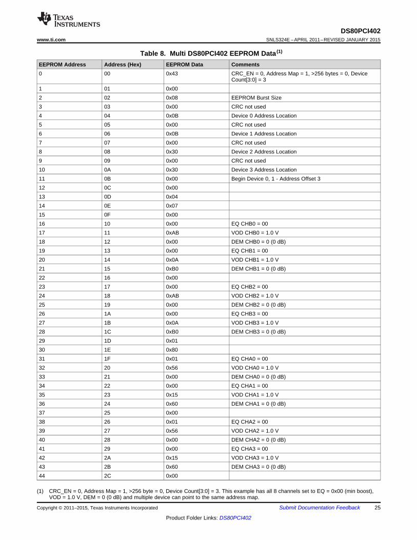
Table 8. Multi DS80PCI402 EEPROM Data (1)
EEPROM Address Address (Hex) EEPROM Data Comments0 00 0x43 CRC_EN = 0, Address Map = 1, >256 bytes = 0, Device
Count[3:0] = 31 01 0x002 02 0x08 EEPROM Burst Size3 03 0x00 CRC not used4 04 0x0B Device 0 Address Location5 05 0x00 CRC not used6 06 0x0B Device 1 Address Location7 07 0x00 CRC not used8 08 0x30 Device 2 Address Location9 09 0x00 CRC not used10 0A 0x30 Device 3 Address Location11 0B 0x00 Begin Device 0, 1 - Address Offset 312 0C 0x0013 0D 0x0414 0E 0x0715 0F 0x0016 10 0x00 EQ CHB0 = 0017 11 0xAB VOD CHB0 = 1.0 V18 12 0x00 DEM CHB0 = 0 (0 dB)19 13 0x00 EQ CHB1 = 0020 14 0x0A VOD CHB1 = 1.0 V21 15 0xB0 DEM CHB1 = 0 (0 dB)22 16 0x0023 17 0x00 EQ CHB2 = 0024 18 0xAB VOD CHB2 = 1.0 V25 19 0x00 DEM CHB2 = 0 (0 dB)26 1A 0x00 EQ CHB3 = 0027 1B 0x0A VOD CHB3 = 1.0 V28 1C 0xB0 DEM CHB3 = 0 (0 dB)29 1D 0x0130 1E 0x8031 1F 0x01 EQ CHA0 = 0032 20 0x56 VOD CHA0 = 1.0 V33 21 0x00 DEM CHA0 = 0 (0 dB)34 22 0x00 EQ CHA1 = 0035 23 0x15 VOD CHA1 = 1.0 V36 24 0x60 DEM CHA1 = 0 (0 dB)37 25 0x0038 26 0x01 EQ CHA2 = 0039 27 0x56 VOD CHA2 = 1.0 V40 28 0x00 DEM CHA2 = 0 (0 dB)41 29 0x00 EQ CHA3 = 0042 2A 0x15 VOD CHA3 = 1.0 V43 2B 0x60 DEM CHA3 = 0 (0 dB)44 2C 0x00
(1) CRC_EN = 0, Address Map = 1, >256 byte = 0, Device Count[3:0] = 3. This example has all 8 channels set to EQ = 0x00 (min boost),VOD = 1.0 V, DEM = 0 (0 dB) and multiple device can point to the same address map.
Copyright © 2011–2015, Texas Instruments Incorporated Submit Documentation Feedback 25
Product Folder Links: DS80PCI402

DS80PCI402SNLS324E –APRIL 2011–REVISED JANUARY 2015 www.ti.com
Table 8. Multi DS80PCI402 EEPROM Data(1) (continued)EEPROM Address Address (Hex) EEPROM Data Comments45 2D 0x0046 2E 0x5447 2F 0x54 End Device 0, 1 - Address Offset 3948 30 0x00 Begin Device 2, 3 - Address Offset 349 31 0x0050 32 0x0451 33 0x0752 34 0x0053 35 0x00 EQ CHB0 = 0054 36 0xAB VOD CHB0 = 1.0 V55 37 0x00 DEM CHB0 = 0 (0 dB)56 38 0x00 EQ CHB1 = 0057 39 0x0A VOD CHB1 = 1.0 V58 3A 0xB0 DEM CHB1 = 0 (0 dB)59 3B 0x0060 3C 0x00 EQ CHB2 = 0061 3D 0xAB VOD CHB2 = 1.0 V62 3E 0x00 DEM CHB2 = 0 (0 dB)63 3F 0x00 EQ CHB3 = 0064 40 0x0A VOD CHB3 = 1.0 V65 41 0xB0 DEM CHB3 = 0 (0 dB)66 42 0x0167 43 0x8068 44 0x01 EQ CHA0 = 0069 45 0x56 VOD CHA0 = 1.0 V70 46 0x00 DEM CHA0 = 0 (0 dB)71 47 0x00 EQ CHA1 = 0072 48 0x15 VOD CHA1 = 1.0 V73 49 0x60 DEM CHA1 = 0 (0 dB)74 4A 0x0075 4B 0x01 EQ CHA2 = 0076 4C 0x56 VOD CHA2 = 1.0 V77 4D 0x00 DEM CHA2 = 0 (0 dB)78 4E 0x00 EQ CHA3 = 0079 4F 0x15 VOD CHA3 = 1.0 V80 50 0x60 DEM CHA3 = 0 (0 dB)81 51 0x0082 52 0x0083 53 0x5484 54 0x54 End Device 2, 3 - Address Offset 39
26 Submit Documentation Feedback Copyright © 2011–2015, Texas Instruments Incorporated
Product Folder Links: DS80PCI402

DS80PCI402www.ti.com SNLS324E –APRIL 2011–REVISED JANUARY 2015
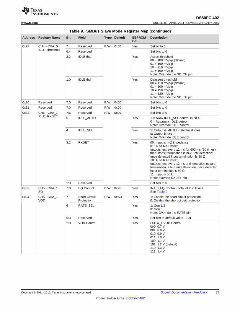
Table 9. SMBus Slave Mode Register MapAddress Register Name Bit Field Type Default EEPROM Description
Bit0x00 Device Address 7 Reserved R/W 0x00 Set bit to 0
Observation 6:3 Address Bit R Observation of AD[3:0] bitsAD[3:0] [6]: AD3
[5]: AD2[4]: AD1[3]: AD0See Table 6
2 EEPROM Read R 1: Device completed the read from externalDone EEPROM
1:0 Reserved R/W Reserved0x01 PWDN Channels 7:0 PWDN CHx R/W 0x00 Yes Power Down per Channel
[7]: CH7 – CHA_3[6]: CH6 – CHA_2[5]: CH5 – CHA_1[4]: CH4 – CHA_0[3]: CH3 – CHB_3[2]: CH2 – CHB_2[1]: CH1 – CHB_1[0]: CH0 – CHB_00x00 = all channels enabled0xFF = all channels disabledNote: override PRSNT pin
0x02 Override PRSNT, 7 Override R/W 0x00 1 = Override Automatic Rx Detect StateLPBK Control RXDET Machine Reset
6 RXDET Value 1 = Set Rx Detect State Machine Reset0 = Clear Rx Detect State Machine Reset
5:4 LPBK Yes 00: Use LPBK pin controlControl 01: INA_n to OUTB_n loopback
10: INB_n to OUTA_n loopback11: Disable loopback and ignore LPBK pin
3:2 Reserved Yes Set bits to 01 Reserved Set bit to 00 Override Yes 1: Block PRSNT pin control
PRSNT 0: Allow PRSNT pin controlpin
0x03 Reserved 7:0 Reserved R/W 0x00 Set bits to 00x04 Reserved 7:0 Reserved R/W 0x00 Yes Set bits to 00x05 Reserved 7:0 Reserved R/W 0x00 Set bits to 00x06 Slave Register 7:5 Reserved R/W 0x10 Set bits to 0
Control 4 Reserved Yes Set bit to 13 Register Enable 1 = Enables SMBus Slave Mode Register
ControlNote: To change VOD, DEM, and EQ of thechannels in slave mode, this bit must be setto 1.
2:0 Reserved Set bits to 00x07 Digital Reset 7 Reserved R/W 0x01 Set bit to 0
Control 6 Reset Registers Self clearing bit, set to 1 to reset the register todefault values.
5:0 Reserved Set bits to 000001'b
Copyright © 2011–2015, Texas Instruments Incorporated Submit Documentation Feedback 27
Product Folder Links: DS80PCI402

DS80PCI402SNLS324E –APRIL 2011–REVISED JANUARY 2015 www.ti.com
Table 9. SMBus Slave Mode Register Map (continued)Address Register Name Bit Field Type Default EEPROM Description
Bit0x08 Override 7 Reserved R/W 0x00 Set bit to 0
Pin Control 6 Override SD_TH Yes 1: Block SD_TH pin control0: Allow SD_TH pin control
5 Reserved Yes Set bit to 04 Override IDLE Yes 1: IDLE control by registers
0: IDLE control by signal detect3 Override Yes 1: Block RXDET pin control
RXDET 0: Allow RXDET pin control2 Override RATE Yes 1: Block RATE pin control
0: Allow RATE pin control1:0 Reserved Set bits to 0
0x09 Reserved 7:0 Reserved R/W 0x00 Set bits to 00x0A Signal Detect 7:0 SD_TH Status R 0x00 CH7 - CH0 Internal Signal Detector Indicator
Monitor [7]: CH7 - CHA_3[6]: CH6 - CHA_2[5]: CH5 - CHA_1[4]: CH4 - CHA_0[3]: CH3 - CHB_3[2]: CH2 - CHB_2[1]: CH1 - CHB_1[0]: CH0 - CHB_00 = Signal detected at input (active data)1 = Signal not detected at input (idle state)NOTE: These bits only function when RATE pin= FLOAT.
0x0B Reserved 7 Reserved R/W 0x00 Set bits to 06:0 Reserved R/W 0x70 Yes Set bits to 111 0000'b
0x0C Reserved 7:0 Reserved R/W 0x00 Set bits to 00x0D Reserved 7:0 Reserved R/W 0x00 Set bits to 00x0E CH0 - CHB_0 7:6 Reserved R/W 0x00 Set bits to 0
IDLE, RXDET 5 IDLE_AUTO Yes 1 = Allow IDLE_SEL control in bit 40 = Automatic IDLE detectNote: Override IDLE control
4 IDLE_SEL Yes 1: Output is MUTED (electrical idle)0: Output is ONNote: Override IDLE control
3:2 RXDET Yes 00: Input is hi-Z impedance01: Auto RX-Detect,outputs test every 12 ms for 600 ms (50 times)then stops; termination is hi-Z until detection;once detected input termination is 50 Ω10: Auto RX-Detect,outputs test every 12 ms until detection occurs;termination is hi-Z until detection; once detectedinput termination is 50 Ω11: Input is 50 ΩNote: Override RXDET pin
1:0 Reserved Set bits to 00x0F CH0 - CHB_0 7:0 EQ Control R/W 0x2F Yes INB_0 EQ Control - total of 256 levels
EQ See Table 2
28 Submit Documentation Feedback Copyright © 2011–2015, Texas Instruments Incorporated
Product Folder Links: DS80PCI402

DS80PCI402www.ti.com SNLS324E –APRIL 2011–REVISED JANUARY 2015
Table 9. SMBus Slave Mode Register Map (continued)Address Register Name Bit Field Type Default EEPROM Description
Bit0x10 CH0 - CHB_0 7 Short Circuit R/W 0xAD Yes 1: Enable the short circuit protection
VOD Protection 0: Disable the short circuit protection6 RATE_SEL Yes 1: Gen 1/2
0: Gen 3Note: Override the RATE pin
5:3 Reserved Yes Set bits to default value - 1012:0 VOD Control Yes OUTB_0 VOD Control
000: 0.7 V001: 0.8 V010: 0.9 V011: 1.0 V100: 1.1 V101: 1.2 V (default)110: 1.3 V111: 1.4 V
0x11 CH0 - CHB_0 7 RXDET R 0x02 Observation bit for RXDET CH0 - CHB_0DEM STATUS 1: RX = detected
0: RX = not detected6:5 RATE_DET R Observation bit for RATE_DET CH0 - CHB_0
STATUS 00: GEN1 (2.5G)01: GEN2 (5G)11: GEN3 (8G)
4:3 Reserved R/W Set bits to 02:0 DEM Control R/W Yes OUTB_0 DEM Control
000: 0 dB001: –1.5 dB010: –3.5 dB (default)011: –5 dB100: –6 dB101: –8 dB110: –9 dB111: –12 dB
0x12 CH0 - CHB_0 7 Reserved R/W 0x00 Yes Set bit to 0IDLE Threshold 6:4 Reserved Set bits to 0
3:2 IDLE tha Yes Assert threshold00 = 180 mVp-p (default)01 = 160 mVp-p10 = 210 mVp-p11 = 190 mVp-pNote: Override the SD_TH pin
1:0 IDLE thd Yes Deassert threshold00 = 110 mVp-p (default)01 = 100 mVp-p10 = 150 mVp-p11 = 130 mVp-pNote: Override the SD_TH pin
0x13 Reserved 7:0 Reserved R/W 0x00 Set bits to 00x14 Reserved 7:0 Reserved R/W 0x00 Set bits to 0
Copyright © 2011–2015, Texas Instruments Incorporated Submit Documentation Feedback 29
Product Folder Links: DS80PCI402

DS80PCI402SNLS324E –APRIL 2011–REVISED JANUARY 2015 www.ti.com
Table 9. SMBus Slave Mode Register Map (continued)Address Register Name Bit Field Type Default EEPROM Description
Bit0x15 CH1 - CHB_1 7:6 Reserved R/W 0x00 Set bits to 0
IDLE, RXDET 5 IDLE_AUTO Yes 1 = Allow IDLE_SEL control in bit 40 = Automatic IDLE detectNote: Override IDLE control
4 IDLE_SEL Yes 1: Output is MUTED (electrical idle)0: Output is ONNote: Override IDLE control
3:2 RXDET Yes 00: Input is hi-Z impedance01: Auto RX-Detect,outputs test every 12 ms for 600 ms (50 times)then stops; termination is hi-Z until detection;once detected input termination is 50 Ω10: Auto RX-Detect,outputs test every 12 ms until detection occurs;termination is hi-Z until detection; once detectedinput termination is 50 Ω11: Input is 50 ΩNote: Override RXDET pin
1:0 Reserved Set bits to 0.0x16 CH1 - CHB_1 7:0 EQ Control R/W 0x2F Yes INB_1 EQ Control - total of 256 levels.
EQ See Table 20x17 CH1 - CHB_1 7 Short Circuit R/W 0xAD Yes 1: Enable the short circuit protection
VOD Protection 0: Disable the short circuit protection6 RATE_SEL Yes 1: Gen 1/2
0: Gen 3Note: Override the RATE pin
5:3 Reserved Yes Set bits to default value - 1012:0 VOD Control Yes OUTB_1 VOD Control
000: 0.7 V001: 0.8 V010: 0.9 V011: 1.0 V100: 1.1 V101: 1.2 V (default)110: 1.3 V111: 1.4 V
0x18 CH1 - CHB_1 7 RXDET R 0x02 Observation bit for RXDET CH1 - CHB_1DEM STATUS 1: RX = detected
0: RX = not detected6:5 RATE_DET R Observation bit for RATE_DET CH1 - CHB_1
STATUS 00: GEN1 (2.5G)01: GEN2 (5G)11: GEN3 (8G)
4:3 Reserved R/W Set bits to 02:0 DEM Control R/W Yes OUTB_1 DEM Control
000: 0 dB001: –1.5 dB010: –3.5 dB (default)011: –5 dB100: –6 dB101: –8 dB110: –9 dB111: –12 dB
30 Submit Documentation Feedback Copyright © 2011–2015, Texas Instruments Incorporated
Product Folder Links: DS80PCI402

DS80PCI402www.ti.com SNLS324E –APRIL 2011–REVISED JANUARY 2015
Table 9. SMBus Slave Mode Register Map (continued)Address Register Name Bit Field Type Default EEPROM Description
Bit0x19 CH1 - CHB_1 7 Reserved R/W 0x00 Yes Set bit to 0.
IDLE Threshold 6:4 Reserved Set bits to 0.3:2 IDLE tha Yes Assert threshold
00 = 180 mVp-p (default)01 = 160 mVp-p10 = 210 mVp-p11 = 190 mVp-pNote: Override the SD_TH pin
1:0 IDLE thd Yes Deassert threshold00 = 110 mVp-p (default)01 = 100 mVp-p10 = 150 mVp-p11 = 130 mVp-pNote: Override the SD_TH pin
0x1A Reserved 7:0 Reserved R/W 0x00 Set bits to 00x1B Reserved 7:0 Reserved R/W 0x00 Set bits to 00x1C CH2 - CHB_2 7:6 Reserved R/W 0x00 Set bits to 0
IDLE, RXDET 5 IDLE_AUTO Yes 1 = Allow IDLE_SEL control in bit 40 = Automatic IDLE detectNote: Override IDLE control
4 IDLE_SEL Yes 1: Output is MUTED (electrical idle)0: Output is ONNote: Override IDLE control
3:2 RXDET Yes 00: Input is hi-Z impedance01: Auto RX-Detect,outputs test every 12 ms for 600 ms (50 times)then stops; termination is hi-Z until detection;once detected input termination is 50 Ω10: Auto RX-Detect,outputs test every 12 ms until detection occurs;termination is hi-Z until detection; once detectedinput termination is 50 Ω11: Input is 50 ΩNote: Override RXDET pin
1:0 Reserved Set bits to 00x1D CH2 - CHB_2 7:0 EQ Control R/W 0x2F Yes INB_2 EQ Control - total of 256 levels.
EQ See Table 20x1E CH2 - CHB_2 7 Short Circuit R/W 0xAD Yes 1: Enable the short circuit protection
VOD Protection 0: Disable the short circuit protection6 RATE_SEL Yes 1: Gen 1/2
0: Gen 3Note: Override the RATE pin
5:3 Reserved Yes Set bits to default value - 1012:0 VOD Control Yes OUTB_2 VOD Control
000: 0.7 V001: 0.8 V010: 0.9 V011: 1.0 V100: 1.1 V101: 1.2 V (default)110: 1.3 V111: 1.4 V
Copyright © 2011–2015, Texas Instruments Incorporated Submit Documentation Feedback 31
Product Folder Links: DS80PCI402

DS80PCI402SNLS324E –APRIL 2011–REVISED JANUARY 2015 www.ti.com
Table 9. SMBus Slave Mode Register Map (continued)Address Register Name Bit Field Type Default EEPROM Description
Bit0x1F CH2 - CHB_2 7 RXDET R 0x02 Observation bit for RXDET CH2 - CHB_2
DEM STATUS 1: RX = detected0: RX = not detected
6:5 RATE_DET R Observation bit for RATE_DET CH2 - CHB_2STATUS 00: GEN1 (2.5G)
01: GEN2 (5G)11: GEN3 (8G)
4:3 Reserved R/W Set bits to 0.2:0 DEM Control R/W Yes OUTB_2 DEM Control
000: 0 dB001: –1.5 dB010: –3.5 dB (default)011: –5 dB100: –6 dB101: –8 dB110: –9 dB111: –12 dB
0x20 CH2 - CHB_2 7 Reserved R/W 0x00 Yes Set bit to 0IDLE Threshold 6:4 Reserved Set bits to 0
3:2 IDLE tha Yes Assert threshold00 = 180 mVp-p (default)01 = 160 mVp-p10 = 210 mVp-p11 = 190 mVp-pNote: Override the SD_TH pin.Set bits to 0
1:0 IDLE thd Yes Deassert threshold00 = 110 mVp-p (default)01 = 100 mVp-p10 = 150 mVp-p11 = 130 mVp-pNote: Override the SD_TH pin
0x21 Reserved 7:0 Reserved R/W 0x00 Set bits to 00x22 Reserved 7:0 Reserved R/W 0x00 Set bits to 00x23 CH3 - CHB_3 7:6 Reserved R/W 0x00 Set bits to 0
IDLE, RXDET 5 IDLE_AUTO Yes 1 = Allow IDLE_SEL control in bit 40 = Automatic IDLE detectNote: Override IDLE control
4 IDLE_SEL Yes 1: Output is MUTED (electrical idle)0: Output is ONNote: Override IDLE control.
3:2 RXDET Yes 00: Input is hi-Z impedance01: Auto RX-Detect,outputs test every 12 ms for 600 ms (50 times)then stops; termination is hi-Z until detection;once detected input termination is 50 Ω10: Auto RX-Detect,outputs test every 12 ms until detection occurs;termination is hi-Z until detection; once detectedinput termination is 50 Ω11: Input is 50 ΩNote: Override RXDET pin
1:0 Reserved Set bits to 00x24 CH3 - CHB_3 7:0 EQ Control R/W 0x2F Yes INB_3 EQ Control - total of 256 levels.
EQ See Table 2
32 Submit Documentation Feedback Copyright © 2011–2015, Texas Instruments Incorporated
Product Folder Links: DS80PCI402

DS80PCI402www.ti.com SNLS324E –APRIL 2011–REVISED JANUARY 2015
Table 9. SMBus Slave Mode Register Map (continued)Address Register Name Bit Field Type Default EEPROM Description
Bit0x25 CH3 - CHB_3 7 Short Circuit R/W 0xAD Yes 1: Enable the short circuit protection
VOD Protection 0: Disable the short circuit protection6 RATE_SEL Yes 1: Gen 1/2
0: Gen 3Note: Override the RATE pin
5:3 Reserved Yes Set bits to default value - 1012:0 VOD Control Yes OUTB_3 VOD Control
000: 0.7 V001: 0.8 V010: 0.9 V011: 1.0 V100: 1.1 V101: 1.2 V (default)110: 1.3 V111: 1.4 V
0x26 CH3 - CHB_3 7 RXDET R 0x02 Observation bit for RXDET CH3 - CHB_3DEM STATUS 1: RX = detected
0: RX = not detected6:5 RATE_DET R Observation bit for RATE_DET CH3 - CHB_3
STATUS 00: GEN1 (2.5G)01: GEN2 (5G)11: GEN3 (8G)
4:3 Reserved R/W Set bits to 02:0 DEM Control R/W Yes OUTB_3 DEM Control
000: 0 dB001: –1.5 dB010: –3.5 dB (default)011: –5 dB100: –6 dB101: –8 dB110: –9 dB111: –12 dB
0x27 CH3 - CHB_3 7 Reserved R/W 0x00 Yes Set bit to 0IDLE Threshold 6:4 Reserved Set bits to 0
3:2 IDLE tha Yes Assert threshold00 = 180 mVp-p (default)01 = 160 mVp-p10 = 210 mVp-p11 = 190 mVp-pNote: Override the SD_TH pin
1:0 IDLE thd Yes Deassert threshold00 = 110 mVp-p (default)01 = 100 mVp-p10 = 150 mVp-p11 = 130 mVp-pNote: Override the SD_TH pin
0x28 Signal Detect 7 Reserved R/W 0x0C Set bit to 0Status Control 6 Reserved Yes Set bit to 0
5:4 High SD_TH Yes Enable Higher Range of Signal Detect StatusStatus Thresholds
[5]: CH0 - CH3[4]: CH4 - CH7
3:2 Fast Signal Yes Enable Fast Signal Detect StatusDetect Status [3]: CH0 - CH3
[2]: CH4 - CH7Note: In Fast Signal Detect, assert/deassertresponse occurs after approximately 3-4 ns
1:0 Reduced SD Yes Enable Reduced Signal Detect Status GainStatus Gain [1]: CH0 - CH3
[0]: CH4 - CH7
Copyright © 2011–2015, Texas Instruments Incorporated Submit Documentation Feedback 33
Product Folder Links: DS80PCI402

DS80PCI402SNLS324E –APRIL 2011–REVISED JANUARY 2015 www.ti.com
Table 9. SMBus Slave Mode Register Map (continued)Address Register Name Bit Field Type Default EEPROM Description
Bit0x29 Reserved 7:0 Reserved R/W 0x00 Set bits to 00x2A Reserved 7:0 Reserved R/W 0x00 Set bits to 00x2B CH4 - CHA_0 7:6 Reserved R/W 0x00 Set bits to 0
IDLE, RXDET 5 IDLE_AUTO Yes 1 = Allow IDLE_SEL control in bit 40 = Automatic IDLE detectNote: Override IDLE control
4 IDLE_SEL Yes 1: Output is MUTED (electrical idle)0: Output is ONNote: Override IDLE control
3:2 RXDET Yes 00: Input is hi-Z impedance01: Auto RX-Detect,outputs test every 12 ms for 600 ms (50 times)then stops; termination is hi-Z until detection;once detected input termination is 50 Ω10: Auto RX-Detect,outputs test every 12 ms until detection occurs;termination is hi-Z until detection; once detectedinput termination is 50 Ω11: Input is 50 ΩNote: Override RXDET pin
1:0 Reserved Set bits to 00x2C CH4 - CHA_0 7:0 EQ Control R/W 0x2F Yes INA_0 EQ Control - total of 256 levels
EQ See Table 20x2D CH4 - CHA_0 7 Short Circuit R/W 0xAD Yes 1: Enable the short circuit protection
VOD Protection 0: Disable the short circuit protection6 RATE_SEL Yes 1: Gen 1/2
0: Gen 3Note: Override the RATE pin
5:3 Reserved Yes Set bits to default value - 1012:0 VOD Control Yes OUTA_0 VOD Control
000: 0.7 V001: 0.8 V010: 0.9 V011: 1.0 V100: 1.1 V101: 1.2 V (default)110: 1.3 V111: 1.4 V
0x2E CH4 - CHA_0 7 RXDET R 0x02 Observation bit for RXDET CH4 - CHA_0DEM STATUS 1: RX = detected
0: RX = not detected6:5 RATE_DET R Observation bit for RATE_DET CH4 - CHA_0
STATUS 00: GEN1 (2.5G)01: GEN2 (5G)11: GEN3 (8G)
4:3 Reserved R/W Set bits to 02:0 DEM Control R/W Yes OUTA_0 DEM Control
000: 0 dB001: –1.5 dB010: –3.5 dB (default)011: –5 dB100: –6 dB101: –8 dB110: –9 dB111: –12 dB
34 Submit Documentation Feedback Copyright © 2011–2015, Texas Instruments Incorporated
Product Folder Links: DS80PCI402
DS80PCI402www.ti.com SNLS324E –APRIL 2011–REVISED JANUARY 2015
Table 9. SMBus Slave Mode Register Map (continued)Address Register Name Bit Field Type Default EEPROM Description
Bit0x2F CH4 - CHA_0 7 Reserved R/W 0x00 Yes Set bit to 0
IDLE Threshold 6:4 Reserved Set bits to 03:2 IDLE tha Yes Assert threshold
00 = 180 mVp-p (default)01 = 160 mVp-p10 = 210 mVp-p11 = 190 mVp-pNote: Override the SD_TH pin
1:0 IDLE thd Yes Deassert threshold00 = 110 mVp-p (default)01 = 100 mVp-p10 = 150 mVp-p11 = 130 mVp-pNote: Override the SD_TH pin
0x30 Reserved 7:0 Reserved R/W 0x00 Set bits to 00x31 Reserved 7:0 Reserved R/W 0x00 Set bits to 00x32 CH5 - CHA_1 7:6 Reserved R/W 0x00 Set bits to 0
IDLE, RXDET 5 IDLE_AUTO Yes 1 = Allow IDLE_SEL control in bit 40 = Automatic IDLE detectNote: Override IDLE control
4 IDLE_SEL Yes 1: Output is MUTED (electrical idle)0: Output is ONNote: Override IDLE control
3:2 RXDET Yes 00: Input is hi-Z impedance01: Auto RX-Detect,outputs test every 12 ms for 600 ms (50 times)then stops; termination is hi-Z until detection;once detected input termination is 50 Ω10: Auto RX-Detect,outputs test every 12 ms until detection occurs;termination is hi-Z until detection; once detectedinput termination is 50 Ω11: Input is 50 ΩNote: override RXDET pin
1:0 Reserved Set bits to 00x33 CH5 - CHA_1 7:0 EQ Control R/W 0x2F Yes INA_1 EQ Control - total of 256 levels
EQ See Table 20x34 CH5 - CHA_1 7 Short Circuit R/W 0xAD Yes 1: Enable the short circuit protection
VOD Protection 0: Disable the short circuit protection6 RATE_SEL Yes 1: Gen 1/2
0: Gen 3Note: Override the RATE pin
5:3 Reserved Yes Set bits to default value - 1012:0 VOD Control Yes OUTA_1 VOD Control
000: 0.7 V001: 0.8 V010: 0.9 V011: 1.0 V100: 1.1 V101: 1.2 V (default)110: 1.3 V111: 1.4 V
Copyright © 2011–2015, Texas Instruments Incorporated Submit Documentation Feedback 35
Product Folder Links: DS80PCI402

DS80PCI402SNLS324E –APRIL 2011–REVISED JANUARY 2015 www.ti.com
Table 9. SMBus Slave Mode Register Map (continued)Address Register Name Bit Field Type Default EEPROM Description
Bit0x35 CH5 - CHA_1 7 RXDET R 0x02 Observation bit for RXDET CH5 - CHA_1
DEM STATUS 1: RX = detected0: RX = not detected
6:5 RATE_DET R Observation bit for RATE_DET CH5 - CHA_1STATUS 00: GEN1 (2.5G)
01: GEN2 (5G)11: GEN3 (8G)
4:3 Reserved R/W Set bits to 02:0 DEM Control R/W Yes OUTA_1 DEM Control
000: 0 dB001: –1.5 dB010: –3.5 dB (default)011: –5 dB100: –6 dB101: –8 dB110: –9 dB111: –12 dB
0x36 CH5 - CHA_1 7 Reserved R/W 0x00 Yes Set bit to 0IDLE Threshold 6:4 Reserved Set bits to 0
3:2 IDLE tha Yes Assert threshold00 = 180 mVp-p (default)01 = 160 mVp-p10 = 210 mVp-p11 = 190 mVp-pNote: Override the SD_TH pin
1:0 IDLE thd Yes Deassert threshold00 = 110 mVp-p (default)01 = 100 mVp-p10 = 150 mVp-p11 = 130 mVp-pNote: Override the SD_TH pin
0x37 Reserved 7:0 Reserved R/W 0x00 Set bits to 00x38 Reserved 7:0 Reserved R/W 0x00 Set bits to 00x39 CH6 - CHA_2 7:6 Reserved R/W 0x00 Set bits to 0
IDLE, RXDET 5 IDLE_AUTO Yes 1 = Allow IDLE_SEL control in bit 40 = Automatic IDLE detectNote: Override IDLE control
4 IDLE_SEL Yes 1: Output is MUTED (electrical idle)0: Output is ONNote: Override IDLE control
3:2 RXDET Yes 00: Input is hi-Z impedance01: Auto RX-Detect,outputs test every 12 ms for 600 ms (50 times)then stops; termination is hi-Z until detection;once detected input termination is 50 Ω10: Auto RX-Detect,outputs test every 12 ms until detection occurs;termination is hi-Z until detection; once detectedinput termination is 50 Ω11: Input is 50 ΩNote: Override RXDET pin
1:0 Reserved Set bits to 00x3A CH6 - CHA_2 7:0 EQ Control R/W 0x2F Yes INA_2 EQ Control - total of 256 levels
EQ See Table 2
36 Submit Documentation Feedback Copyright © 2011–2015, Texas Instruments Incorporated
Product Folder Links: DS80PCI402

DS80PCI402www.ti.com SNLS324E –APRIL 2011–REVISED JANUARY 2015
Table 9. SMBus Slave Mode Register Map (continued)Address Register Name Bit Field Type Default EEPROM Description
Bit0x3B CH6 - CHA_2 7 Short Circuit R/W 0xAD Yes 1: Enable the short circuit protection
VOD Protection 0: Disable the short circuit protection6 RATE_SEL Yes 1: Gen 1/2
0: Gen 3Note: Override the RATE pin
5:3 Reserved Yes Set bits to default value - 1012:0 VOD Control Yes OUTA_2 VOD Control
000: 0.7 V001: 0.8 V010: 0.9 V011: 1.0 V100: 1.1 V101: 1.2 V (default)110: 1.3 V111: 1.4 V
0x3C CH6 - CHA_2 7 RXDET R 0x02 Observation bit for RXDET CH6 - CHA_2DEM STATUS 1: RX = detected
0: RX = not detected6:5 RATE_DET R Observation bit for RATE_DET CH6 - CHA_2
STATUS 00: GEN1 (2.5G)01: GEN2 (5G)11: GEN3 (8G)
4:3 Reserved R/W Set bits to 02:0 DEM Control R/W Yes OUTA_2 DEM Control
000: 0 dB001: –1.5 dB010: –3.5 dB (default)011: –5 dB100: –6 dB101: –8 dB110: –9 dB111: –12 dB
0x3D CH6 - CHA_2 7 Reserved R/W 0x00 Yes Set bit to 0IDLE Threshold 6:4 Reserved Set bits to 0
3:2 IDLE tha Yes Assert threshold00 = 180 mVp-p (default)01 = 160 mVp-p10 = 210 mVp-p11 = 190 mVp-pNote: Override the SD_TH pin
1:0 IDLE thd Yes Deassert threshold00 = 110 mVp-p (default)01 = 100 mVp-p10 = 150 mVp-p11 = 130 mVp-pNote: Override the SD_TH pin
0x3E Reserved 7:0 Reserved R/W 0x00 Set bits to 00x3F Reserved 7:0 Reserved R/W 0x00 Set bits to 0
Copyright © 2011–2015, Texas Instruments Incorporated Submit Documentation Feedback 37
Product Folder Links: DS80PCI402
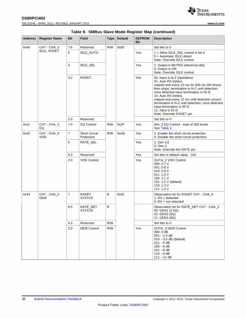
DS80PCI402SNLS324E –APRIL 2011–REVISED JANUARY 2015 www.ti.com
Table 9. SMBus Slave Mode Register Map (continued)Address Register Name Bit Field Type Default EEPROM Description
Bit0x40 CH7 - CHA_3 7:6 Reserved R/W 0x00 Set bits to 0
IDLE, RXDET 5 IDLE_AUTO Yes 1 = Allow IDLE_SEL control in bit 40 = Automatic IDLE detectNote: Override IDLE control
4 IDLE_SEL Yes 1: Output is MUTED (electrical idle)0: Output is ONNote: Override IDLE control
3:2 RXDET Yes 00: Input is hi-Z impedance01: Auto RX-Detect,outputs test every 12 ms for 600 ms (50 times)then stops; termination is hi-Z until detection;once detected input termination is 50 Ω10: Auto RX-Detect,outputs test every 12 ms until detection occurs;termination is hi-Z until detection; once detectedinput termination is 50 Ω11: Input is 50 ΩNote: Override RXDET pin
1:0 Reserved Set bits to 00x41 CH7 - CHA_3 7:0 EQ Control R/W 0x2F Yes INA_3 EQ Control - total of 256 levels
EQ See Table 20x42 CH7 - CHA_3 7 Short Circuit R/W 0xAD Yes 1: Enable the short circuit protection
VOD Protection 0: Disable the short circuit protection6 RATE_SEL Yes 1: Gen 1/2
0: Gen 3Note: Override the RATE pin
5:3 Reserved Yes Set bits to default value - 1012:0 VOD Control Yes OUTA_3 VOD Control
000: 0.7 V001: 0.8 V010: 0.9 V011: 1.0 V100: 1.1 V101: 1.2 V (default)110: 1.3 V111: 1.4 V
0x43 CH7 - CHA_3 7 RXDET R 0x02 Observation bit for RXDET CH7 - CHA_3DEM STATUS 1: RX = detected
0: RX = not detected6:5 RATE_DET R Observation bit for RATE_DET CH7 - CHA_3
STATUS 00: GEN1 (2.5G)01: GEN2 (5G)11: GEN3 (8G)
4:3 Reserved R/W Set bits to 02:0 DEM Control R/W Yes OUTA_3 DEM Control
000: 0 dB001: –1.5 dB010: –3.5 dB (default)011: –5 dB100: –6 dB101: –8 dB110: –9 dB111: –12 dB
38 Submit Documentation Feedback Copyright © 2011–2015, Texas Instruments Incorporated
Product Folder Links: DS80PCI402

DS80PCI402www.ti.com SNLS324E –APRIL 2011–REVISED JANUARY 2015
Table 9. SMBus Slave Mode Register Map (continued)Address Register Name Bit Field Type Default EEPROM Description
Bit0x44 CH7 - CHA_3 7 Reserved R/W 0x00 Yes Set bit to 0
IDLE Threshold 6:4 Reserved Set bits to 03:2 IDLE tha Yes Assert threshold
00 = 180 mVp-p (default)01 = 160 mVp-p10 = 210 mVp-p11 = 190 mVp-pNote: Override the SD_TH pin
1:0 IDLE thd Yes Deassert threshold00 = 110 mVp-p (default)01 = 100 mVp-p10 = 150 mVp-p11 = 130 mVp-pNote: Override the SD_TH pin
0x45 Reserved 7:0 Reserved R/W 0x00 Set bits to 00x46 Reserved 7:0 Reserved R/W 0x38 Set bits to 0x380x47 Reserved 7:4 Reserved R/W 0x00 Set bits to 0
3:0 Reserved R/W Yes Set bits to 00x48 Reserved 7:6 Reserved R/W 0x05 Yes Set bits to 0
5:0 Reserved R/W Set bits to 00 0101'b0x49 Reserved 7:0 Reserved R/W 0x00 Set bits to 00x4A Reserved 7:0 Reserved R/W 0x00 Set bits to 00x4B Reserved 7:0 Reserved R/W 0x00 Set bits to 00x4C Reserved 7:3 Reserved R/W 0x00 Yes Set bits to 0
2:1 Reserved R/W Set bits to 00 Reserved R/W Yes Set bits to 0
0x4D Reserved 7:0 Reserved R/W 0x00 Set bits to 00x4E Reserved 7:0 Reserved R/W 0x00 Set bits to 00x4F Reserved 7:0 Reserved R/W 0x00 Set bits to 00x50 Reserved 7:0 Reserved R/W 0x00 Set bits to 00x51 Device ID 7:5 VERSION R 0x44 010'b
4:0 ID 00100'b0x52 Reserved 7:0 Reserved R/W 0x00 Set bits to 00x53 Reserved 7:0 Reserved R/W 0x00 Set bits to 00x54 Reserved 7:0 Reserved R/W 0x00 Set bits to 00x55 Reserved 7:0 Reserved R/W 0x00 Set bits to 00x56 Reserved 7:0 Reserved R/W 0x10 Set bits to 0x100x57 Reserved 7:0 Reserved R/W 0x64 Set bits to 0x640x58 Reserved 7:0 Reserved R/W 0x21 Set bits to 0x210x59 Reserved 7:1 Reserved R/W 0x00 Set bits to 0
0 Reserved Yes Set bit to 00x5A Reserved 7:0 Reserved R/W 0x54 Yes Set bits to 0x540x5B Reserved 7:0 Reserved R/W 0x54 Yes Set bits to 0x540x5C Reserved 7:0 Reserved R/W 0x00 Set bits to 00x5D Reserved 7:0 Reserved R/W 0x00 Set bits to 00x5E Reserved 7:0 Reserved R/W 0x00 Set bits to 00x5F Reserved 7:0 Reserved R/W 0x00 Set bits to 00x60 Reserved 7:0 Reserved R/W 0x00 Set bits to 00x61 Reserved 7:0 Reserved R/W 0x00 Set bits to 0
Copyright © 2011–2015, Texas Instruments Incorporated Submit Documentation Feedback 39
Product Folder Links: DS80PCI402

DS80PCI402SNLS324E –APRIL 2011–REVISED JANUARY 2015 www.ti.com
9 Application and Implementation
NOTEInformation in the following applications sections is not part of the TI componentspecification, and TI does not warrant its accuracy or completeness. TI’s customers areresponsible for determining suitability of components for their purposes. Customers shouldvalidate and test their design implementation to confirm system functionality.
9.1 Application InformationIn PCIe Gen-3 applications, the specification requires Rx-Tx link training to establish and optimize signalconditioning settings at 8 Gbps. In link training, the Rx partner requests a series of FIR - preshoot and de-emphasis coefficients (10 Presets) from the Tx partner. The Rx partner includes 7-levels (6 dB to 12 dB) of CTLEfollowed by a single tap DFE. The link training would pre-condition the signal with an equalized link between theroot-complex and endpoint. Note that there is no link training in PCIe Gen-1 (2.5 Gbps) or PCIe Gen-2 (5.0Gbps) applications. The DS80PCI402 is placed in between the Tx and Rx. It would help extend the PCB tracereach distance by boosting the attenuated signals with its equalization, so that the signal can be more easilyrecovered by the downstream Rx. In Gen 3 mode, DS80PCI402 transmit outputs are designed to pass the TxPreset signaling onto the Rx for the PCIe Gen 3 link to train and optimize the equalization settings. Thesuggested setting for the DS80PCI402 are EQ=00, VOD = 1.2 Vp-p and DEM = 0 dB. Additional adjustments toincrease the EQ or DEM setting should be performed to optimize the eye opening in the Rx partner. See thetables below for Pin Mode and SMBus Mode configurations.
Table 10. Suggested Device Settings in Pin ModeCHANNEL PIN MODE SETTINGSEQx[1:0] 0, 0 (Level 1)
DEMx[1:0] Float, R (Level 10)
Table 11. Suggested Device Settings in SMBus Slave ModeREGISTER WRITE VALUE COMMENTS
0x06 0x18 Enables SMBus Slave Mode Register Control0x0F 0x00 Set CHB_0 EQ to 0x00.0x10 0xAD Set CHB_0 VOD to 101'b (1.2 Vp-p).0x11 0x00 Set CHB_0 DEM to 000'b (0 dB).0x16 0x00 Set CHB_1 EQ to 0x00.0x17 0xAD Set CHB_1 VOD to 101'b (1.2 Vp-p).0x18 0x00 Set CHB_1 DEM to 000'b (0 dB).0x1D 0x00 Set CHB_2 EQ to 0x00.0x1E 0xAD Set CHB_2 VOD to 101'b (1.2 Vp-p).0x1F 0x00 Set CHB_2 DEM to 000'b (0 dB).0x24 0x00 Set CHB_3 EQ to 0x00.0x25 0xAD Set CHB_3 VOD to 101'b (1.2 Vp-p).0x26 0x00 Set CHB_3 DEM to 000'b (0 dB).0x2C 0x00 Set CHA_0 EQ to 0x00.0x2D 0xAD Set CHA_0 VOD to 101'b (1.2 Vp-p).0x2E 0x00 Set CHA_0 DEM to 000'b (0 dB).0x33 0x00 Set CHA_1 EQ to 0x00.0x34 0xAD Set CHA_1 VOD to 101'b (1.2 Vp-p).0x35 0x00 Set CHA_1 DEM to 000'b (0 dB).0x3A 0x00 Set CHA_2 EQ to 0x00.0x3B 0xAD Set CHA_2 VOD to 101'b (1.2 Vp-p).0x3C 0x00 Set CHA_2 DEM to 000'b (0 dB).
40 Submit Documentation Feedback Copyright © 2011–2015, Texas Instruments Incorporated
Product Folder Links: DS80PCI402
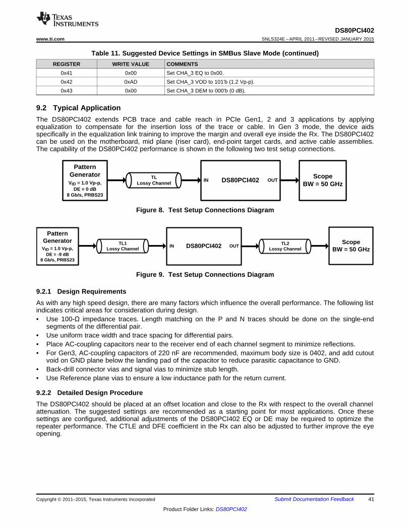
PatternGeneratorVID = 1.0 Vp-p,
DE = -9 dB8 Gb/s, PRBS23
ScopeBW = 50 GHzDS80PCI402TL1
Lossy ChannelIN OUT TL2
Lossy Channel
PatternGeneratorVID = 1.0 Vp-p,
DE = 0 dB8 Gb/s, PRBS23
ScopeBW = 50 GHz
DS80PCI402IN OUTTLLossy Channel
DS80PCI402www.ti.com SNLS324E –APRIL 2011–REVISED JANUARY 2015
Table 11. Suggested Device Settings in SMBus Slave Mode (continued)REGISTER WRITE VALUE COMMENTS
0x41 0x00 Set CHA_3 EQ to 0x00.0x42 0xAD Set CHA_3 VOD to 101'b (1.2 Vp-p).0x43 0x00 Set CHA_3 DEM to 000'b (0 dB).
9.2 Typical ApplicationThe DS80PCI402 extends PCB trace and cable reach in PCIe Gen1, 2 and 3 applications by applyingequalization to compensate for the insertion loss of the trace or cable. In Gen 3 mode, the device aidsspecifically in the equalization link training to improve the margin and overall eye inside the Rx. The DS80PCI402can be used on the motherboard, mid plane (riser card), end-point target cards, and active cable assemblies.The capability of the DS80PCI402 performance is shown in the following two test setup connections.
Figure 8. Test Setup Connections Diagram
Figure 9. Test Setup Connections Diagram
9.2.1 Design RequirementsAs with any high speed design, there are many factors which influence the overall performance. The following listindicates critical areas for consideration during design.• Use 100-Ω impedance traces. Length matching on the P and N traces should be done on the single-end
segments of the differential pair.• Use uniform trace width and trace spacing for differential pairs.• Place AC-coupling capacitors near to the receiver end of each channel segment to minimize reflections.• For Gen3, AC-coupling capacitors of 220 nF are recommended, maximum body size is 0402, and add cutout
void on GND plane below the landing pad of the capacitor to reduce parasitic capacitance to GND.• Back-drill connector vias and signal vias to minimize stub length.• Use Reference plane vias to ensure a low inductance path for the return current.
9.2.2 Detailed Design ProcedureThe DS80PCI402 should be placed at an offset location and close to the Rx with respect to the overall channelattenuation. The suggested settings are recommended as a starting point for most applications. Once thesesettings are configured, additional adjustments of the DS80PCI402 EQ or DE may be required to optimize therepeater performance. The CTLE and DFE coefficient in the Rx can also be adjusted to further improve the eyeopening.
Copyright © 2011–2015, Texas Instruments Incorporated Submit Documentation Feedback 41
Product Folder Links: DS80PCI402

DS80PCI402SNLS324E –APRIL 2011–REVISED JANUARY 2015 www.ti.com
Typical Application (continued)9.2.3 Application Curves
DS80PCI402 Settings: DS80PCI402 Settings:EQ[1:0] = [R, R] or 0x15, Dem[1:0] = [Float, Float] EQ[1:0] = [Float, R] or 0x1F, DEM[1:0] = [Float, Float]
Figure 10. TL = 20-Inch 4–Mil FR4 Trace Figure 11. TL = 35-Inch 4–Mil FR4 Trace
DS80PCI402 Settings:DS80PCI402 Settings:EQ[1:0] = [R, 1] or 0x0F, DEM[1:0] = [Float, Float]EQ[1:0] = [R, R] or 0x15, DEM[1:0] = [Float, Float]
Figure 13. TL1 = 30-Inch 4–Mil FR4 Trace, TL2 = 15-InchFigure 12. TL1 = 20-Inch 4–Mil FR4 Trace, TL2 = 15-Inch4–Mil FR4 Trace4–Mil FR4 Trace
42 Submit Documentation Feedback Copyright © 2011–2015, Texas Instruments Incorporated
Product Folder Links: DS80PCI402

DS80PCI402www.ti.com SNLS324E –APRIL 2011–REVISED JANUARY 2015
10 Power Supply Recommendations
10.1 3.3-V or 2.5-V Supply Mode OperationThe DS80PCI402 has an optional internal voltage regulator to provide the 2.5-V supply to the device. In 3.3-Vmode, the VIN pin = 3.3 V is used to supply power to the device and the VDD pins should be left open. Theinternal regulator will provide the 2.5 V to the VDD pins of the device and a 0.1-µF capacitor is needed at each ofthe five VDD pins for power supply de-coupling (total capacitance should be ≤ 0.5 µF), and the VDD pins shouldbe left open. The VDD_SEL pin must be tied to GND to enable the internal regulator. In 2.5-V mode, the VIN pinshould be left open and 2.5 V supply must be applied to the VDD pins. The VDD_SEL pin must be left open (noconnect) to disable the internal regulator.
The DS80PCI402 can be configured for 2.5-V operation or 3.3-V operation. The lists below outline requiredconnections for each supply selection.
3.3-V Mode of Operation1. Tie VDD_SEL = 0 with 1-kΩ resistor to GND.2. Feed 3.3-V supply into VIN pin. Local 1.0 µF decoupling at VIN is recommended.3. See information on VDD bypass below.4. SDA and SCL pins should connect pullup resistor to VIN5. Any 4-Level input which requires a connection to "Logic 1" should use a 1-kΩ resistor to VIN
2.5-V Mode of Operation6. VDD_SEL = Float7. VIN = Float8. Feed 2.5-V supply into VDD pins.9. See information on VDD bypass below.10. SDA and SCL pins connect pullup resistor to VDD for 2.5 V uC SMBus IO11. SDA and SCL pins connect pullup resistor to VDD for 3.3 V uC SMBus IO12. Any 4-Level input which requires a connection to "Logic 1" should use a 1-kΩ resistor to VIN
Copyright © 2011–2015, Texas Instruments Incorporated Submit Documentation Feedback 43
Product Folder Links: DS80PCI402

VDD_SEL
VIN
VDD
VDD
VDD
VDD
VDD
3.3V
0.1 uF
0.1 uF
0.1 uF
0.1 uF
0.1 uF
Internal voltage
regulator
Enable
2.5V
VDD_SEL
VIN
VDD
VDD
VDD
VDD
VDD
Internal voltage
regulator
Disable
Place 0.1 uF close to VDD PinTotal capacitance should be 7 0.5 uF
1 uF
10 u
F
2.5V
1 uF
10 u
F0.1 uF
0.1 uF
0.1 uF
0.1 uF
0.1 uF
Place capcitors close to VDD Pin
open
openCapacitors can be either tantalum or an ultra-low ESR seramic.
3.3V mode 2.5V mode
Capacitors can be either tantalum or an ultra-low ESR seramic.
DS80PCI402SNLS324E –APRIL 2011–REVISED JANUARY 2015 www.ti.com
3.3-V or 2.5-V Supply Mode Operation (continued)
Figure 14. 3.3 V or 2.5 V Supply Connection Diagram
10.2 Power Supply BypassingTwo approaches are recommended to ensure that the DS80PCI402 is provided with an adequate power supplybypass. First, the supply (VDD) and ground (GND) pins should be connected to power planes routed on adjacentlayers of the printed circuit board. Second, careful attention to supply bypassing through the proper use ofbypass capacitors is required. A 0.1-μF bypass capacitor should be connected to each VDD pin such that thecapacitor is placed as close as possible to the device. Small body size capacitors (such as 0402) reduce theparasitic inductance of the capacitor and also help in placement close to the VDD pin. If possible, the layerthickness of the dielectric should be minimized so that the VDD and GND planes create a low inductance supplywith distributed capacitance.
44 Submit Documentation Feedback Copyright © 2011–2015, Texas Instruments Incorporated
Product Folder Links: DS80PCI402
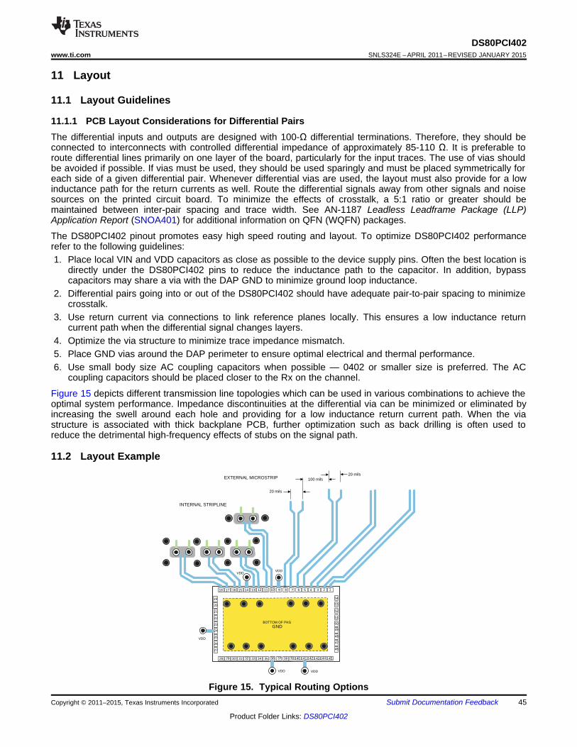
46
47
48
49
50
51
52
53
54
4342414039383736
22
27
26
25
24
23
21
20
19
4544
345678910 12
GNDBOTTOM OF PKG
131415161718 1112
333231302928 3534
VDD
VDD
VDD
VDD
100 mils
20 mils
20 mils
VDD
INTERNAL STRIPLINE
EXTERNAL MICROSTRIP
DS80PCI402www.ti.com SNLS324E –APRIL 2011–REVISED JANUARY 2015
11 Layout
11.1 Layout Guidelines
11.1.1 PCB Layout Considerations for Differential PairsThe differential inputs and outputs are designed with 100-Ω differential terminations. Therefore, they should beconnected to interconnects with controlled differential impedance of approximately 85-110 Ω. It is preferable toroute differential lines primarily on one layer of the board, particularly for the input traces. The use of vias shouldbe avoided if possible. If vias must be used, they should be used sparingly and must be placed symmetrically foreach side of a given differential pair. Whenever differential vias are used, the layout must also provide for a lowinductance path for the return currents as well. Route the differential signals away from other signals and noisesources on the printed circuit board. To minimize the effects of crosstalk, a 5:1 ratio or greater should bemaintained between inter-pair spacing and trace width. See AN-1187 Leadless Leadframe Package (LLP)Application Report (SNOA401) for additional information on QFN (WQFN) packages.
The DS80PCI402 pinout promotes easy high speed routing and layout. To optimize DS80PCI402 performancerefer to the following guidelines:1. Place local VIN and VDD capacitors as close as possible to the device supply pins. Often the best location is
directly under the DS80PCI402 pins to reduce the inductance path to the capacitor. In addition, bypasscapacitors may share a via with the DAP GND to minimize ground loop inductance.
2. Differential pairs going into or out of the DS80PCI402 should have adequate pair-to-pair spacing to minimizecrosstalk.
3. Use return current via connections to link reference planes locally. This ensures a low inductance returncurrent path when the differential signal changes layers.
4. Optimize the via structure to minimize trace impedance mismatch.5. Place GND vias around the DAP perimeter to ensure optimal electrical and thermal performance.6. Use small body size AC coupling capacitors when possible — 0402 or smaller size is preferred. The AC
coupling capacitors should be placed closer to the Rx on the channel.
Figure 15 depicts different transmission line topologies which can be used in various combinations to achieve theoptimal system performance. Impedance discontinuities at the differential via can be minimized or eliminated byincreasing the swell around each hole and providing for a low inductance return current path. When the viastructure is associated with thick backplane PCB, further optimization such as back drilling is often used toreduce the detrimental high-frequency effects of stubs on the signal path.
11.2 Layout Example
Figure 15. Typical Routing OptionsCopyright © 2011–2015, Texas Instruments Incorporated Submit Documentation Feedback 45
Product Folder Links: DS80PCI402
DS80PCI402SNLS324E –APRIL 2011–REVISED JANUARY 2015 www.ti.com
12 Device and Documentation Support
12.1 Device Support
12.1.1 Third-Party Products DisclaimerTI'S PUBLICATION OF INFORMATION REGARDING THIRD-PARTY PRODUCTS OR SERVICES DOES NOTCONSTITUTE AN ENDORSEMENT REGARDING THE SUITABILITY OF SUCH PRODUCTS OR SERVICESOR A WARRANTY, REPRESENTATION OR ENDORSEMENT OF SUCH PRODUCTS OR SERVICES, EITHERALONE OR IN COMBINATION WITH ANY TI PRODUCT OR SERVICE.
12.2 TrademarksPCI-Express is a trademark of PCI-SIG.All other trademarks are the property of their respective owners.
12.3 Electrostatic Discharge CautionThese devices have limited built-in ESD protection. The leads should be shorted together or the device placed in conductive foamduring storage or handling to prevent electrostatic damage to the MOS gates.
12.4 GlossarySLYZ022 — TI Glossary.
This glossary lists and explains terms, acronyms, and definitions.
13 Mechanical, Packaging, and Orderable InformationThe following pages include mechanical, packaging, and orderable information. This information is the mostcurrent data available for the designated devices. This data is subject to change without notice and revision ofthis document. For browser-based versions of this data sheet, refer to the left-hand navigation.
46 Submit Documentation Feedback Copyright © 2011–2015, Texas Instruments Incorporated
Product Folder Links: DS80PCI402

PACKAGE OPTION ADDENDUM
www.ti.com 23-Aug-2014
Addendum-Page 1
PACKAGING INFORMATION
Orderable Device Status(1)
Package Type PackageDrawing
Pins PackageQty
Eco Plan(2)
Lead/Ball Finish(6)
MSL Peak Temp(3)
Op Temp (°C) Device Marking(4/5)
Samples
DS80PCI402SQ/NOPB ACTIVE WQFN NJY 54 2000 Green (RoHS& no Sb/Br)
CU SN Level-2-260C-1 YEAR -40 to 85 DS80PCI402SQ
DS80PCI402SQE/NOPB ACTIVE WQFN NJY 54 250 Green (RoHS& no Sb/Br)
CU SN Level-2-260C-1 YEAR -40 to 85 DS80PCI402SQ
(1) The marketing status values are defined as follows:ACTIVE: Product device recommended for new designs.LIFEBUY: TI has announced that the device will be discontinued, and a lifetime-buy period is in effect.NRND: Not recommended for new designs. Device is in production to support existing customers, but TI does not recommend using this part in a new design.PREVIEW: Device has been announced but is not in production. Samples may or may not be available.OBSOLETE: TI has discontinued the production of the device.
(2) Eco Plan - The planned eco-friendly classification: Pb-Free (RoHS), Pb-Free (RoHS Exempt), or Green (RoHS & no Sb/Br) - please check http://www.ti.com/productcontent for the latest availabilityinformation and additional product content details.TBD: The Pb-Free/Green conversion plan has not been defined.Pb-Free (RoHS): TI's terms "Lead-Free" or "Pb-Free" mean semiconductor products that are compatible with the current RoHS requirements for all 6 substances, including the requirement thatlead not exceed 0.1% by weight in homogeneous materials. Where designed to be soldered at high temperatures, TI Pb-Free products are suitable for use in specified lead-free processes.Pb-Free (RoHS Exempt): This component has a RoHS exemption for either 1) lead-based flip-chip solder bumps used between the die and package, or 2) lead-based die adhesive used betweenthe die and leadframe. The component is otherwise considered Pb-Free (RoHS compatible) as defined above.Green (RoHS & no Sb/Br): TI defines "Green" to mean Pb-Free (RoHS compatible), and free of Bromine (Br) and Antimony (Sb) based flame retardants (Br or Sb do not exceed 0.1% by weightin homogeneous material)
(3) MSL, Peak Temp. - The Moisture Sensitivity Level rating according to the JEDEC industry standard classifications, and peak solder temperature.
(4) There may be additional marking, which relates to the logo, the lot trace code information, or the environmental category on the device.
(5) Multiple Device Markings will be inside parentheses. Only one Device Marking contained in parentheses and separated by a "~" will appear on a device. If a line is indented then it is a continuationof the previous line and the two combined represent the entire Device Marking for that device.
(6) Lead/Ball Finish - Orderable Devices may have multiple material finish options. Finish options are separated by a vertical ruled line. Lead/Ball Finish values may wrap to two lines if the finishvalue exceeds the maximum column width.
Important Information and Disclaimer:The information provided on this page represents TI's knowledge and belief as of the date that it is provided. TI bases its knowledge and belief on informationprovided by third parties, and makes no representation or warranty as to the accuracy of such information. Efforts are underway to better integrate information from third parties. TI has taken andcontinues to take reasonable steps to provide representative and accurate information but may not have conducted destructive testing or chemical analysis on incoming materials and chemicals.TI and TI suppliers consider certain information to be proprietary, and thus CAS numbers and other limited information may not be available for release.
PACKAGE OPTION ADDENDUM
www.ti.com 23-Aug-2014
Addendum-Page 2
In no event shall TI's liability arising out of such information exceed the total purchase price of the TI part(s) at issue in this document sold by TI to Customer on an annual basis.

TAPE AND REEL INFORMATION
*All dimensions are nominal
Device PackageType
PackageDrawing
Pins SPQ ReelDiameter
(mm)
ReelWidth
W1 (mm)
A0(mm)
B0(mm)
K0(mm)
P1(mm)
W(mm)
Pin1Quadrant
DS80PCI402SQ/NOPB WQFN NJY 54 2000 330.0 16.4 5.8 10.3 1.0 12.0 16.0 Q1
DS80PCI402SQE/NOPB WQFN NJY 54 250 178.0 16.4 5.8 10.3 1.0 12.0 16.0 Q1
PACKAGE MATERIALS INFORMATION
www.ti.com 20-Sep-2016
Pack Materials-Page 1
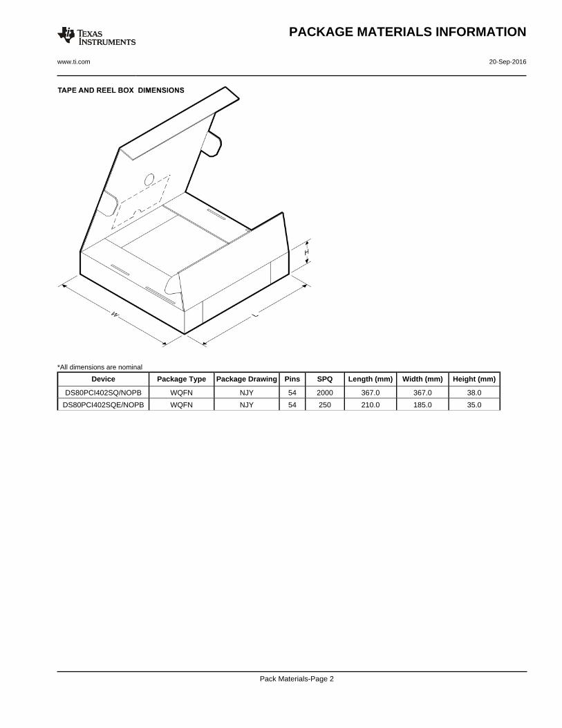
*All dimensions are nominal
Device Package Type Package Drawing Pins SPQ Length (mm) Width (mm) Height (mm)
DS80PCI402SQ/NOPB WQFN NJY 54 2000 367.0 367.0 38.0
DS80PCI402SQE/NOPB WQFN NJY 54 250 210.0 185.0 35.0
PACKAGE MATERIALS INFORMATION
www.ti.com 20-Sep-2016
Pack Materials-Page 2

www.ti.com
PACKAGE OUTLINE
C
54X 0.30.2
3.51±0.1
50X 0.5
54X 0.50.3
0.8 MAX
2X8.5
7.5±0.1
2X 4
A
10.19.9
B 5.65.4
0.30.2
0.50.3
(0.1)
4214993/A 07/2013
WQFNNJY0054AWQFN
PIN 1 INDEX AREA
SEATING PLANE
1
18 28
45
19 27
54 46
0.1 C A B0.05 C
(OPTIONAL)PIN 1 ID
DETAILSEE TERMINAL
NOTES: 1. All linear dimensions are in millimeters. Dimensions in parenthesis are for reference only. Dimensioning and tolerancing per ASME Y14.5M.2. This drawing is subject to change without notice. 3. The package thermal pad must be soldered to the printed circuit board for thermal and mechanical performance.
SCALE 2.000
DETAILOPTIONAL TERMINAL
TYPICAL
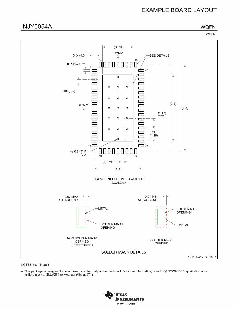
www.ti.com
EXAMPLE BOARD LAYOUT
(3.51)
0.07 MINALL AROUND
0.07 MAXALL AROUND
54X (0.6)
54X (0.25)
(9.8)
(5.3)
( ) TYPVIA
0.2
50X (0.5)
2X(1.16)
(1) TYP
(7.5)
(1.17)TYP
4214993/A 07/2013
WQFNNJY0054AWQFN
SYMMSEE DETAILS
1
18
19 27
28
45
4654
SYMM
LAND PATTERN EXAMPLESCALE:8X
NOTES: (continued) 4. This package is designed to be soldered to a thermal pad on the board. For more information, refer to QFN/SON PCB application note in literature No. SLUA271 (www.ti.com/lit/slua271).
SOLDER MASKOPENING
METAL
SOLDER MASKDEFINED
METAL
SOLDER MASKOPENING
SOLDER MASK DETAILS
NON SOLDER MASKDEFINED
(PREFERRED)

www.ti.com
EXAMPLE STENCIL DESIGN
(1.17)TYP
(5.3)
54X (0.6)
54X (0.25)
12X (1.51)
(9.8)
(0.855) TYP
12X (0.97)
50X (0.5)
4214993/A 07/2013
WQFNNJY0054AWQFN
NOTES: (continued) 5. Laser cutting apertures with trapezoidal walls and rounded corners may offer better paste release. IPC-7525 may have alternate design recommendations.
SYMM
TYPMETAL
SOLDERPASTE EXAMPLEBASED ON 0.125mm THICK STENCIL
EXPOSED PAD
67% PRINTED SOLDER COVERAGE BY AREASCALE:10X
1
18
19 27
28
45
4654
SYMM

IMPORTANT NOTICE
Texas Instruments Incorporated and its subsidiaries (TI) reserve the right to make corrections, enhancements, improvements and otherchanges to its semiconductor products and services per JESD46, latest issue, and to discontinue any product or service per JESD48, latestissue. Buyers should obtain the latest relevant information before placing orders and should verify that such information is current andcomplete. All semiconductor products (also referred to herein as “components”) are sold subject to TI’s terms and conditions of salesupplied at the time of order acknowledgment.TI warrants performance of its components to the specifications applicable at the time of sale, in accordance with the warranty in TI’s termsand conditions of sale of semiconductor products. Testing and other quality control techniques are used to the extent TI deems necessaryto support this warranty. Except where mandated by applicable law, testing of all parameters of each component is not necessarilyperformed.TI assumes no liability for applications assistance or the design of Buyers’ products. Buyers are responsible for their products andapplications using TI components. To minimize the risks associated with Buyers’ products and applications, Buyers should provideadequate design and operating safeguards.TI does not warrant or represent that any license, either express or implied, is granted under any patent right, copyright, mask work right, orother intellectual property right relating to any combination, machine, or process in which TI components or services are used. Informationpublished by TI regarding third-party products or services does not constitute a license to use such products or services or a warranty orendorsement thereof. Use of such information may require a license from a third party under the patents or other intellectual property of thethird party, or a license from TI under the patents or other intellectual property of TI.Reproduction of significant portions of TI information in TI data books or data sheets is permissible only if reproduction is without alterationand is accompanied by all associated warranties, conditions, limitations, and notices. TI is not responsible or liable for such altereddocumentation. Information of third parties may be subject to additional restrictions.Resale of TI components or services with statements different from or beyond the parameters stated by TI for that component or servicevoids all express and any implied warranties for the associated TI component or service and is an unfair and deceptive business practice.TI is not responsible or liable for any such statements.Buyer acknowledges and agrees that it is solely responsible for compliance with all legal, regulatory and safety-related requirementsconcerning its products, and any use of TI components in its applications, notwithstanding any applications-related information or supportthat may be provided by TI. Buyer represents and agrees that it has all the necessary expertise to create and implement safeguards whichanticipate dangerous consequences of failures, monitor failures and their consequences, lessen the likelihood of failures that might causeharm and take appropriate remedial actions. Buyer will fully indemnify TI and its representatives against any damages arising out of the useof any TI components in safety-critical applications.In some cases, TI components may be promoted specifically to facilitate safety-related applications. With such components, TI’s goal is tohelp enable customers to design and create their own end-product solutions that meet applicable functional safety standards andrequirements. Nonetheless, such components are subject to these terms.No TI components are authorized for use in FDA Class III (or similar life-critical medical equipment) unless authorized officers of the partieshave executed a special agreement specifically governing such use.Only those TI components which TI has specifically designated as military grade or “enhanced plastic” are designed and intended for use inmilitary/aerospace applications or environments. Buyer acknowledges and agrees that any military or aerospace use of TI componentswhich have not been so designated is solely at the Buyer's risk, and that Buyer is solely responsible for compliance with all legal andregulatory requirements in connection with such use.TI has specifically designated certain components as meeting ISO/TS16949 requirements, mainly for automotive use. In any case of use ofnon-designated products, TI will not be responsible for any failure to meet ISO/TS16949.
Products ApplicationsAudio www.ti.com/audio Automotive and Transportation www.ti.com/automotiveAmplifiers amplifier.ti.com Communications and Telecom www.ti.com/communicationsData Converters dataconverter.ti.com Computers and Peripherals www.ti.com/computersDLP® Products www.dlp.com Consumer Electronics www.ti.com/consumer-appsDSP dsp.ti.com Energy and Lighting www.ti.com/energyClocks and Timers www.ti.com/clocks Industrial www.ti.com/industrialInterface interface.ti.com Medical www.ti.com/medicalLogic logic.ti.com Security www.ti.com/securityPower Mgmt power.ti.com Space, Avionics and Defense www.ti.com/space-avionics-defenseMicrocontrollers microcontroller.ti.com Video and Imaging www.ti.com/videoRFID www.ti-rfid.comOMAP Applications Processors www.ti.com/omap TI E2E Community e2e.ti.comWireless Connectivity www.ti.com/wirelessconnectivity
Mailing Address: Texas Instruments, Post Office Box 655303, Dallas, Texas 75265Copyright © 2016, Texas Instruments Incorporated