dspic30f5011/5013 data sheet - microchip...
TRANSCRIPT

© 2011 Microchip Technology Inc. DS70116J
dsPIC30F5011/5013Data Sheet
High-Performance,16-bit Digital Signal Controllers

Note the following details of the code protection feature on Microchip devices:• Microchip products meet the specification contained in their particular Microchip Data Sheet.
• Microchip believes that its family of products is one of the most secure families of its kind on the market today, when used in the intended manner and under normal conditions.
• There are dishonest and possibly illegal methods used to breach the code protection feature. All of these methods, to our knowledge, require using the Microchip products in a manner outside the operating specifications contained in Microchip’s Data Sheets. Most likely, the person doing so is engaged in theft of intellectual property.
• Microchip is willing to work with the customer who is concerned about the integrity of their code.
• Neither Microchip nor any other semiconductor manufacturer can guarantee the security of their code. Code protection does not mean that we are guaranteeing the product as “unbreakable.”
Code protection is constantly evolving. We at Microchip are committed to continuously improving the code protection features of ourproducts. Attempts to break Microchip’s code protection feature may be a violation of the Digital Millennium Copyright Act. If such actsallow unauthorized access to your software or other copyrighted work, you may have a right to sue for relief under that Act.
Information contained in this publication regarding deviceapplications and the like is provided only for your convenienceand may be superseded by updates. It is your responsibility toensure that your application meets with your specifications.MICROCHIP MAKES NO REPRESENTATIONS ORWARRANTIES OF ANY KIND WHETHER EXPRESS ORIMPLIED, WRITTEN OR ORAL, STATUTORY OROTHERWISE, RELATED TO THE INFORMATION,INCLUDING BUT NOT LIMITED TO ITS CONDITION,QUALITY, PERFORMANCE, MERCHANTABILITY ORFITNESS FOR PURPOSE. Microchip disclaims all liabilityarising from this information and its use. Use of Microchipdevices in life support and/or safety applications is entirely atthe buyer’s risk, and the buyer agrees to defend, indemnify andhold harmless Microchip from any and all damages, claims,suits, or expenses resulting from such use. No licenses areconveyed, implicitly or otherwise, under any Microchipintellectual property rights.
DS70116J-page 2
Trademarks
The Microchip name and logo, the Microchip logo, dsPIC, KEELOQ, KEELOQ logo, MPLAB, PIC, PICmicro, PICSTART, PIC32 logo, rfPIC and UNI/O are registered trademarks of Microchip Technology Incorporated in the U.S.A. and other countries.
FilterLab, Hampshire, HI-TECH C, Linear Active Thermistor, MXDEV, MXLAB, SEEVAL and The Embedded Control Solutions Company are registered trademarks of Microchip Technology Incorporated in the U.S.A.
Analog-for-the-Digital Age, Application Maestro, CodeGuard, dsPICDEM, dsPICDEM.net, dsPICworks, dsSPEAK, ECAN, ECONOMONITOR, FanSense, HI-TIDE, In-Circuit Serial Programming, ICSP, Mindi, MiWi, MPASM, MPLAB Certified logo, MPLIB, MPLINK, mTouch, Omniscient Code Generation, PICC, PICC-18, PICDEM, PICDEM.net, PICkit, PICtail, REAL ICE, rfLAB, Select Mode, Total Endurance, TSHARC, UniWinDriver, WiperLock and ZENA are trademarks of Microchip Technology Incorporated in the U.S.A. and other countries.
SQTP is a service mark of Microchip Technology Incorporated in the U.S.A.
All other trademarks mentioned herein are property of their respective companies.
© 2011, Microchip Technology Incorporated, Printed in the U.S.A., All Rights Reserved.
Printed on recycled paper.
ISBN: 978-1-60932-843-6Microchip received ISO/TS-16949:2002 certification for its worldwide
© 2011 Microchip Technology Inc.
headquarters, design and wafer fabrication facilities in Chandler and Tempe, Arizona; Gresham, Oregon and design centers in California and India. The Company’s quality system processes and procedures are for its PIC® MCUs and dsPIC® DSCs, KEELOQ® code hopping devices, Serial EEPROMs, microperipherals, nonvolatile memory and analog products. In addition, Microchip’s quality system for the design and manufacture of development systems is ISO 9001:2000 certified.

dsPIC30F5011/5013High-Performance, Digital Signal Controllers
High-Performance Modified RISC CPU:• Modified Harvard architecture• C compiler optimized instruction set architecture• Flexible addressing modes• 83 base instructions• 24-bit wide instructions, 16-bit wide data path• 66 Kbytes on-chip Flash program space• 4 Kbytes of on-chip data RAM• 1 Kbyte of nonvolatile data EEPROM • 16 x 16-bit working register array• Up to 30 MIPS operation:
- DC to 40 MHz external clock input- 4 MHz-10 MHz oscillator input with
PLL active (4x, 8x, 16x)• Up to 41 interrupt sources:
- Eight user selectable priority levels- Five external interrupt sources- Four processor traps
DSP Features:• Dual data fetch• Modulo and Bit-Reversed modes• Two 40-bit wide accumulators with optional
saturation logic• 17-bit x 17-bit single cycle hardware fractional/
integer multiplier• All DSP instructions are single cycle
- Multiply-Accumulate (MAC) operation• Single cycle ±16 shift
Peripheral Features:• High-current sink/source I/O pins: 25 mA/25 mA• Five 16-bit timers/counters; optionally pair up
16-bit timers into 32-bit timer modules• 16-bit Capture input functions• 16-bit Compare/PWM output functions• Data Converter Interface (DCI) supports common
audio codec protocols, including I2S and AC’97• 3-wire SPI modules (supports four Frame modes)• I2C™ module supports Multi-Master/Slave mode
and 7-bit/10-bit addressing• Two addressable UART modules with FIFO
buffers• Two CAN bus modules compliant with CAN 2.0B
standard
Analog Features:• 12-bit Analog-to-Digital Converter (ADC) with:
- 200 ksps conversion rate- Up to 16 input channels- Conversion available during Sleep and Idle
• Programmable Low-Voltage Detection (PLVD)• Programmable Brown-out Detection and Reset
generation
Special Microcontroller Features:• Enhanced Flash program memory:
- 10,000 erase/write cycle (min.) for industrial temperature range, 100K (typical)
• Data EEPROM memory:- 100,000 erase/write cycle (min.) for
industrial temperature range, 1M (typical)• Self-reprogrammable under software control• Power-on Reset (POR), Power-up Timer (PWRT)
and Oscillator Start-up Timer (OST)• Flexible Watchdog Timer (WDT) with on-chip
low- power RC oscillator for reliable operation• Fail-Safe Clock Monitor operation:
- Detects clock failure and switches to on-chip low-power RC oscillator
• Programmable code protection• In-Circuit Serial Programming™ (ICSP™)
programming capability• Selectable Power Management modes:
- Sleep, Idle and Alternate Clock modes
Note: This data sheet summarizes features ofthis group of dsPIC30F devices and is notintended to be a complete referencesource. For more information on the CPU,peripherals, register descriptions andgeneral device functionality, refer to the“dsPIC30F Family Reference Manual”(DS70046). For more information on thedevice instruction set and programming,refer to the “16-bit MCU and DSC Pro-grammer’s Reference Manual”(DS70157).
© 2011 Microchip Technology Inc. DS70116J-page 3

dsPIC30F5011/5013
CMOS Technology:• Low-power, high-speed Flash technology• Wide operating voltage range (2.5V to 5.5V)• Industrial and Extended temperature ranges• Low power consumptionTABLE 1: dsPIC30F5011/5013 CONTROLLER FAMILY
Device PinsProgram Memory SRAM
BytesEEPROM
BytesTimer 16-bit
InputCap
Output Comp/Std
PWM
Codec Interface
A/D 12-bit 200 ksps U
AR
T
SPI
I2 C™
CA
N
Bytes Instructions
dsPIC30F5011 64 66K 22K 4096 1024 5 8 8 AC’97, I2S 16 ch 2 2 1 2 dsPIC30F5013 80 66K 22K 4096 1024 5 8 8 AC’97, I2S 16 ch 2 2 1 2
DS70116J-page 4 © 2011 Microchip Technology Inc.

dsPIC30F5011/5013
Pin Diagrams12345678910111213 36
353433
32313029282726
64 63 62 61 60 59 58 57 56
141516
17 18 19 20 21 22 23 24 25
EMUC1/SOSCO/T1CK/CN0/RC14EMUD1/SOSCI/T4CK/CN1/RC13EMUC2/OC1/RD0IC4/INT4/RD11
IC2/INT2/RD9IC1/INT1/RD8VSS
OSC2/CLKO/RC15OSC1/CLKIVDD
SCL/RG2
EMUC3/SCK1/INT0/RF6U1RX/SDI1/RF2EMUD3/U1TX/SDO1/RF3
COFS/RG15T2CK/RC1T3CK/RC2
SCK2/CN8/RG6SDI2/CN9/RG7
SDO2/CN10/RG8MCLR
VSS
VDD
AN3/CN5/RB3AN2/SS1/LVDIN/CN4/RB2
AN1/VREF-/CN3/RB1AN0/VREF+/CN2/RB0
OC
8/C
N16
/RD
7
CSD
O/R
G13
CSD
I/RG
12C
SCK
/RG
14
VS
S
C2T
X/R
G1
C1T
X/R
F1
C2R
X/R
G0
EM
UD
2/O
C2/
RD
1O
C3/
RD
2
PG
C/E
MU
C/A
N6/
OC
FA/R
B6
PGD
/EM
UD
/AN
7/R
B7
AVD
D
AVS
S
AN8/
RB
8AN
9/R
B9
AN
10/R
B10
AN11
/RB1
1V
SS
VD
D
AN
12/R
B12
AN
13/R
B13
AN
14/R
B14
AN
15/O
CFB
/CN
12/R
B15
U2T
X/C
N18
/RF5
U2R
X/C
N17
/RF4
SDA/RG3
43424140393837
44
484746
50 495154 53 5255
45
SS2/CN11/RG9
AN5/IC8/CN7/RB5AN4/IC7/CN6/RB4
IC3/INT3/RD10
VD
D
C1R
X/R
F0
OC
4/R
D3
OC
7/C
N15
/RD
6O
C6/
IC6/
CN
14/R
D5
OC
5/IC
5/C
N13
/RD
4
64-Pin TQFP
dsPIC30F5011
© 2011 Microchip Technology Inc. DS70116J-page 5

dsPIC30F5011/5013
Pin Diagrams (Continued)7274 73 71 70 69 68 67 66 65 64 63 62 61
20
23456789101112
13141516
50494847464544
21
41
4039383736353423 24 25 26 27 28 29 30 31 32 33
dsPIC30F5013
171819
751
57565554535251
605958
4342
7678 777922
80
IC5/
RD
12O
C4/
RD
3O
C3/
RD
2E
MU
D2/
OC
2/R
D1
CS
CK
/RG
14
C2R
X/R
G0
C2T
X/R
G1
C1T
X/R
F1C
1RX
/RF0
CS
DO
/RG
13C
SD
I/RG
12
OC
8/C
N16
/RD
7
OC
6/C
N14
/RD
5
EMUC2/OC1/RD0IC4/RD11
IC2/RD9IC1/RD8INT4/RA15
IC3/RD10
INT3/RA14VSS
OSC1/CLKI
VDD
SCL/RG2
U1RX/RF2U1TX/RF3
EMUC1/SOSCO/T1CK/CN0/RC14EMUD1/SOSCI/CN1/RC13
VRE
F+/R
A10
VRE
F-/R
A9
AVD
D
AVS
S
AN
8/R
B8
AN
9/R
B9
AN
10/R
B10
AN11
/RB
11
VD
D
U2R
X/C
N17
/RF4
IC8/
CN
21/R
D15
U2T
X/C
N18
/RF5
AN
6/O
CFA
/RB
6A
N7/
RB
7
T3CK/RC2T4CK/RC3T5CK/RC4
SCK2/CN8/RG6SDI2/CN9/RG7
SDO2/CN10/RG8MCLR
SS2/CN11/RG9
AN4/CN6/RB4AN3/CN5/RB3
AN2/SS1/LVDIN/CN4/RB2PGC/EMUC/AN1/CN3/RB1PGD/EMUD/AN0/CN2/RB0
VSS
VDD
COFS/RG15T2CK/RC1
INT2/RA13INT1/RA12
AN
12/R
B12
AN
13/R
B13
AN
14/R
B14
AN
15/O
CFB
/CN
12/R
B15
VD
D
VS
S
OC
5/C
N13
/RD
4IC
6/C
N19
/RD
13
SDA/RG3
SDI1/RF7
EMUD3/SDO1/RF8
AN5/CN7/RB5
VS
S
OSC2/CLKO/RC15
OC
7/C
N15
/RD
6
EMUC3/SCK1/INT0/RF6
IC7/
CN
20/R
D14
80-Pin TQFP
CN
23/R
A7C
N22
/RA6
DS70116J-page 6 © 2011 Microchip Technology Inc.
dsPIC30F5011/5013
Table of Contents1.0 Device Overview .......................................................................................................................................................................... 92.0 CPU Architecture Overview........................................................................................................................................................ 153.0 Memory Organization ................................................................................................................................................................. 234.0 Interrupts .................................................................................................................................................................................... 355.0 Address Generator Units............................................................................................................................................................ 416.0 Flash Program Memory.............................................................................................................................................................. 477.0 Data EEPROM Memory ............................................................................................................................................................. 538.0 I/O Ports ..................................................................................................................................................................................... 579.0 Timer1 Module ........................................................................................................................................................................... 6310.0 Timer2/3 Module ........................................................................................................................................................................ 6711.0 Timer4/5 Module ....................................................................................................................................................................... 7312.0 Input Capture Module................................................................................................................................................................. 7713.0 Output Compare Module ............................................................................................................................................................ 8114.0 SPI™ Module ............................................................................................................................................................................. 8715.0 I2C™ Module ............................................................................................................................................................................. 9116.0 Universal Asynchronous Receiver Transmitter (UART) Module ................................................................................................ 9917.0 CAN Module ............................................................................................................................................................................. 10718.0 Data Converter Interface (DCI) Module.................................................................................................................................... 11719.0 12-bit Analog-to-Digital Converter (ADC) Module .................................................................................................................... 12720.0 System Integration ................................................................................................................................................................... 13721.0 Instruction Set Summary .......................................................................................................................................................... 15122.0 Development Support............................................................................................................................................................... 15923.0 Electrical Characteristics .......................................................................................................................................................... 16324.0 Packaging Information.............................................................................................................................................................. 203Index .................................................................................................................................................................................................. 209The Microchip Web Site..................................................................................................................................................................... 215Customer Change Notification Service .............................................................................................................................................. 215Customer Support .............................................................................................................................................................................. 215Reader Response .............................................................................................................................................................................. 216Product Identification System ............................................................................................................................................................ 217TO OUR VALUED CUSTOMERSIt is our intention to provide our valued customers with the best documentation possible to ensure successful use of your Microchipproducts. To this end, we will continue to improve our publications to better suit your needs. Our publications will be refined andenhanced as new volumes and updates are introduced. If you have any questions or comments regarding this publication, please contact the Marketing Communications Department viaE-mail at [email protected] or fax the Reader Response Form in the back of this data sheet to (480) 792-4150. Wewelcome your feedback.
Most Current Data SheetTo obtain the most up-to-date version of this data sheet, please register at our Worldwide Web site at:
http://www.microchip.comYou can determine the version of a data sheet by examining its literature number found on the bottom outside corner of any page.The last character of the literature number is the version number, (e.g., DS30000A is version A of document DS30000).
ErrataAn errata sheet, describing minor operational differences from the data sheet and recommended workarounds, may exist for currentdevices. As device/documentation issues become known to us, we will publish an errata sheet. The errata will specify the revisionof silicon and revision of document to which it applies.To determine if an errata sheet exists for a particular device, please check with one of the following:• Microchip’s Worldwide Web site; http://www.microchip.com• Your local Microchip sales office (see last page)When contacting a sales office, please specify which device, revision of silicon and data sheet (include literature number) you areusing.
Customer Notification SystemRegister on our web site at www.microchip.com to receive the most current information on all of our products.
© 2011 Microchip Technology Inc. DS70116J-page 7

dsPIC30F5011/5013
NOTES:DS70116J-page 8 © 2011 Microchip Technology Inc.

dsPIC30F5011/5013
1.0 DEVICE OVERVIEW
This document contains specific information for thedsPIC30F5011/5013 Digital Signal Controller (DSC)devices. The dsPIC30F5011/5013 devices containextensive Digital Signal Processor (DSP) functionalitywithin a high-performance 16-bit microcontroller (MCU)architecture. Figure 1-1 and Figure 1-2 show deviceblock diagrams for dsPIC30F5011 and dsPIC30F5013,respectively.
Note: This data sheet summarizes features ofthis group of dsPIC30F devices and is notintended to be a complete referencesource. For more information on the CPU,peripherals, register descriptions andgeneral device functionality, refer to the“dsPIC30F Family Reference Manual”(DS70046). For more information on thedevice instruction set and programming,refer to the “16-bit MCU and DSCProgrammer’s Reference Manual”(DS70157).
© 2011 Microchip Technology Inc. DS70116J-page 9

dsPIC30F5011/5013
FIGURE 1-1: dsPIC30F5011 BLOCK DIAGRAMAN8/RB8AN9/RB9AN10/RB10AN11/RB11
Power-upTimer
OscillatorStart-up Timer
POR/BOR
WatchdogTimer
InstructionDecode &Control
OSC1/CLKI
MCLR
VDD, VSS
AN4/IC7/CN6/RB4
AN12/RB12AN13/RB13AN14/RB14AN15/OCFB/CN12/RB15
Low-VoltageDetect
UART1,
CAN2
TimingGeneration
CAN1,
AN5/IC8/CN7/RB5
16
PCH PCLProgram Counter
ALU<16>
16
24
24
24
24
X Data Bus
IR
I2C™
DCI
PGC/EMUC/AN6/OCFA/RB6PGD/EMUD/AN7/RB7
PCU
12-bit ADC
Timers
SCK2/CN8/RG6SDI2/CN9/RG7SDO2/CN10/RG8SS2/CN11/RG9
U2TX/CN18/RF5EMUC3/SCK1/INT0/RF6
Input Capture Module
OutputCompareModule
EMUC1/SOSCO/T1CK/CN0/RC14EMUD1/SOSCI/T4CK/CN1/RC13
T2CK/RC1
PORTB
C1RX/RF0C1TX/RF1U1RX/SDI1/RF2EMUD3/U1TX/SDO1/RF3
C2RX/RG0C2TX/RG1SCL/RG2SDA/RG3
PORTG
PORTD
16
16 16
16 x 16W Reg Array
Divide Unit Engine
DSP
Decode
ROM Latch
16
Y Data Bus
Effective Address
X RAGUX WAGU Y AGU
AN0/VREF+/CN2/RB0AN1/VREF-/CN3/RB1AN2/SS1/LVDIN/CN4/RB2AN3/CN5/RB3
OSC2/CLKO/RC15
U2RX/CN17/RF4
AVDD, AVSS
UART2SPI2
16
16
16
16
16
PORTC
PORTF
16
16
16
16
8
InterruptController PSV & Table
Data AccessControl Block
StackControl Logic
LoopControlLogic
Data LatchData LatchY Data
(2 Kbytes)RAM
X Data
(2 Kbytes)RAM
AddressLatch
AddressLatch
Control Signals to Various Blocks
EMUC2/OC1/RD0EMUD2/OC2/RD1OC3/RD2OC4/RD3OC5/IC5/CN13/RD4OC6/IC6/CN14/RD5OC7/CN15/RD6OC8/CN16/RD7IC1/INT1/RD8IC2/INT2/RD9IC3/INT3/RD10IC4/INT4/RD11
16
CSDI/RG12CSDO/RG13CSCK/RG14COFS/RG15
T3CK/RC2
SPI1,
Address LatchProgram
(66 Kbytes)
Data Latch
Data EEPROM(1 Kbyte)
16
Memory
DS70116J-page 10 © 2011 Microchip Technology Inc.

dsPIC30F5011/5013
FIGURE 1-2: dsPIC30F5013 BLOCK DIAGRAMAN8/RB8AN9/RB9AN10/RB10AN11/RB11
Power-upTimer
OscillatorStart-up Timer
POR/BOR
WatchdogTimer
InstructionDecode &Control
OSC1/CLKI
MCLR
VDD, VSS
AN4/CN6/RB4
AN12/RB12AN13/RB13AN14/RB14AN15/OCFB/CN12/RB15
Low-VoltageDetect
UART1,
INT4/RA15INT3/RA14
VREF+/RA10VREF-/RA9
CAN2
TimingGeneration
CAN1,
AN5/CN7/RB5
16
PCH PCLProgram Counter
ALU<16>
16
24
24
24
24
X Data Bus
IR
I2C™
DCI
AN6/OCFA/RB6AN7/RB7
PCU
12-bit ADC
Timers
SCK2/CN8/RG6SDI2/CN9/RG7SDO2/CN10/RG8SS2/CN11/RG9
U2TX/CN18/RF5EMUC3/SCK1/INT0/RF6SDI1/RF7EMUD3/SDO1/RF8
Input Capture Module
OutputCompareModule
EMUC1/SOSCO/T1CK/CN0/RC14EMUD1/SOSCI/CN1/RC13
T4CK/RC3
T2CK/RC1
PORTB
C1RX/RF0C1TX/RF1U1RX/RF2U1TX/RF3
C2RX/RG0C2TX/RG1SCL/RG2SDA/RG3
PORTG
PORTD
16
16 16
16 x 16W Reg Array
Divide Unit Engine
DSP
Decode
ROM Latch
16
Y Data Bus
Effective Address
X RAGUX WAGU Y AGU
PGD/EMUD/AN0/CN2/RB0PGC/EMUC/AN1/CN3/RB1AN2/SS1/LVDIN/CN4/RB2AN3/CN5/RB3
OSC2/CLKO/RC15
U2RX/CN17/RF4
AVDD, AVSS
UART2SPI2
16
16
16
16
16 PORTA
PORTC
PORTF
16
16
16
16
8
InterruptController PSV & Table
Data AccessControl Block
StackControl Logic
LoopControlLogic
Data LatchData LatchY Data
(2 Kbytes)RAM
X Data
(2 Kbytes)RAM
AddressLatch
AddressLatch
Control Signals to Various Blocks
EMUC2/OC1/RD0EMUD2/OC2/RD1OC3/RD2OC4/RD3OC5/CN13/RD4OC6/CN14/RD5OC7/CN15/RD6OC8/CN16/RD7IC1/RD8IC2/RD9IC3/RD10IC4/RD11IC5/RD12IC6/CN19/RD13IC7/CN20/RD14IC8/CN21/RD15
16
CSDI/RG12CSDO/RG13CSCK/RG14COFS/RG15
T3CK/RC2
SPI1,
INT1/RA12INT2/RA13
CN23/RA7CN22/RA6
T5CK/RC4
Address LatchProgram Memory
(66 Kbytes)
Data Latch
Data EEPROM(1 Kbyte)
16
© 2011 Microchip Technology Inc. DS70116J-page 11

dsPIC30F5011/5013
Table 1-1 provides a brief description of device I/O pin-outs and the functions that may be multiplexed to a portpin. Multiple functions may exist on one port pin. Whenmultiplexing occurs, the peripheral module’s functionalrequirements may force an override of the datadirection of the port pin.TABLE 1-1: PINOUT I/O DESCRIPTIONS
Pin Name PinType
BufferType Description
AN0-AN15 I Analog Analog input channels. AN0 and AN1 are also used for device programming data and clock inputs, respectively.
AVDD P P Positive supply for analog module. This pin must be connected at all times.AVSS P P Ground reference for analog module. This pin must be connected at all times.CLKICLKO
IO
ST/CMOS—
External clock source input. Always associated with OSC1 pin function.Oscillator crystal output. Connects to crystal or resonator in Crystal Oscillator mode. Optionally functions as CLKO in RC and EC modes. Always associated with OSC2 pin function.
CN0-CN23 I ST Input change notification inputs.Can be software programmed for internal weak pull-ups on all inputs.
COFSCSCKCSDICSDO
I/OI/OIO
STSTST—
Data Converter Interface Frame Synchronization pin.Data Converter Interface Serial Clock input/output pin.Data Converter Interface Serial data input pin.Data Converter Interface Serial data output pin.
C1RXC1TXC2RXC2TX
IOIO
ST—ST—
CAN1 Bus Receive pin.CAN1 Bus Transmit pin.CAN2 Bus Receive pin.CAN2 Bus Transmit pin
EMUDEMUCEMUD1EMUC1EMUD2EMUC2EMUD3EMUC3
I/OI/OI/OI/OI/OI/OI/OI/O
STSTSTSTSTSTSTST
ICD Primary Communication Channel data input/output pin.ICD Primary Communication Channel clock input/output pin.ICD Secondary Communication Channel data input/output pin.ICD Secondary Communication Channel clock input/output pin.ICD Tertiary Communication Channel data input/output pin.ICD Tertiary Communication Channel clock input/output pin.ICD Quaternary Communication Channel data input/output pin.ICD Quaternary Communication Channel clock input/output pin.
IC1-IC8 I ST Capture inputs 1 through 8.INT0INT1INT2INT3INT4
IIIII
STSTSTSTST
External interrupt 0.External interrupt 1.External interrupt 2.External interrupt 3.External interrupt 4.
LVDIN I Analog Low-Voltage Detect Reference Voltage input pin.
MCLR I/P ST Master Clear (Reset) input or programming voltage input. This pin is an active low Reset to the device.
OCFAOCFBOC1-OC8
IIO
STST—
Compare Fault A input (for Compare channels 1, 2, 3 and 4).Compare Fault B input (for Compare channels 5, 6, 7 and 8).Compare outputs 1 through 8.
Legend: CMOS = CMOS compatible input or output Analog = Analog input ST = Schmitt Trigger input with CMOS levels O = Output I = Input P = Power
DS70116J-page 12 © 2011 Microchip Technology Inc.

dsPIC30F5011/5013
OSC1
OSC2
I
I/O
ST/CMOS
—
Oscillator crystal input. ST buffer when configured in RC mode; CMOS otherwise.Oscillator crystal output. Connects to crystal or resonator in Crystal Oscillator mode. Optionally functions as CLKO in RC and EC modes.
PGDPGC
I/OI
STST
In-Circuit Serial Programming™ data input/output pin.In-Circuit Serial Programming clock input pin.
RA6-RA7RA9-RA10RA12-RA15
I/OI/OI/O
STSTST
PORTA is a bidirectional I/O port.
RB0-RB15 I/O ST PORTB is a bidirectional I/O port.RC1-RC4RC13-RC15
I/OI/O
STST
PORTC is a bidirectional I/O port.
RD0-RD15 I/O ST PORTD is a bidirectional I/O port.RF0-RF8 I/O ST PORTF is a bidirectional I/O port.RG0-RG3RG6-RG9RG12-RG15
I/OI/OI/O
STSTST
PORTG is a bidirectional I/O port.
SCK1SDI1SDO1SS1SCK2SDI2SDO2SS2
I/OIOI
I/OIOI
STST—STSTST—ST
Synchronous serial clock input/output for SPI1.SPI1 Data In.SPI1 Data Out.SPI1 Slave Synchronization.Synchronous serial clock input/output for SPI2.SPI2 Data In.SPI2 Data Out.SPI2 Slave Synchronization.
SCLSDA
I/OI/O
STST
Synchronous serial clock input/output for I2C™.Synchronous serial data input/output for I2C.
SOSCOSOSCI
OI
—ST/CMOS
32 kHz low-power oscillator crystal output. 32 kHz low-power oscillator crystal input. ST buffer when configured in RC mode; CMOS otherwise.
T1CKT2CKT3CKT4CKT5CK
IIIII
STSTSTSTST
Timer1 external clock input.Timer2 external clock input.Timer3 external clock input.Timer4 external clock input.Timer5 external clock input.
U1RXU1TXU1ARXU1ATXU2RXU2TX
IOIOIO
ST—ST—ST—
UART1 Receive.UART1 Transmit.UART1 Alternate Receive.UART1 Alternate Transmit.UART2 Receive.UART2 Transmit.
VDD P — Positive supply for logic and I/O pins.VSS P — Ground reference for logic and I/O pins.VREF+ I Analog Analog Voltage Reference (High) input.VREF- I Analog Analog Voltage Reference (Low) input.
TABLE 1-1: PINOUT I/O DESCRIPTIONS (CONTINUED)
Pin Name PinType
BufferType Description
Legend: CMOS = CMOS compatible input or output Analog = Analog input ST = Schmitt Trigger input with CMOS levels O = Output I = Input P = Power
© 2011 Microchip Technology Inc. DS70116J-page 13

dsPIC30F5011/5013
NOTES:DS70116J-page 14 © 2011 Microchip Technology Inc.

dsPIC30F5011/5013
2.0 CPU ARCHITECTURE OVERVIEW
2.1 Core OverviewThis section contains a brief overview of the CPUarchitecture of the dsPIC30F. For additional hard-ware and programming information, please refer tothe “dsPIC30F Family Reference Manual” (DS70046)and the “16-bit MCU and DSC Programmer’sReference Manual” (DS70157), respectively.
The core has a 24-bit instruction word. The ProgramCounter (PC) is 23 bits wide with the Least Significantbit (LSb) always clear (refer to Section 3.1 “ProgramAddress Space”), and the Most Significant bit (MSb)is ignored during normal program execution, except forcertain specialized instructions. Thus, the PC canaddress up to 4M instruction words of user programspace. An instruction prefetch mechanism is used tohelp maintain throughput. Program loop constructs,free from loop count management overhead, are sup-ported using the DO and REPEAT instructions, both ofwhich are interruptible at any point.
The working register array consists of 16 x 16-bit regis-ters, each of which can act as data, address or offsetregisters. One working register (W15) operates as asoftware Stack Pointer for interrupts and calls.
The data space is 64 Kbytes (32K words) and is splitinto two blocks, referred to as X and Y data memory.Each block has its own independent Address Genera-tion Unit (AGU). Most instructions operate solelythrough the X memory, AGU, which provides theappearance of a single unified data space. TheMultiply-Accumulate (MAC) class of dual source DSPinstructions operate through both the X and Y AGUs,splitting the data address space into two parts (seeSection 3.2 “Data Address Space”). The X and Ydata space boundary is device specific and cannot bealtered by the user. Each data word consists of 2 bytes,and most instructions can address data either as wordsor bytes.
There are two methods of accessing data stored inprogram memory:
• The upper 32 Kbytes of data space memory can be mapped into the lower half (user space) of pro-gram space at any 16K program word boundary, defined by the 8-bit Program Space Visibility Page (PSVPAG) register. This lets any instruction access program space as if it were data space, with a limitation that the access requires an addi-tional cycle. Moreover, only the lower 16 bits of each instruction word can be accessed using this method.
• Linear indirect access of 32K word pages within program space is also possible using any working register, via table read and write instructions. Table read and write instructions can be used to access all 24 bits of an instruction word.
Overhead-free circular buffers (modulo addressing) aresupported in both X and Y address spaces. This isprimarily intended to remove the loop overhead forDSP algorithms.
The X AGU also supports bit-reversed addressing ondestination effective addresses to greatly simplify inputor output data reordering for radix-2 FFT algorithms.Refer to Section 5.0 “Address Generator Units” fordetails on modulo and bit-reversed addressing.
The core supports Inherent (no operand), Relative,Literal, Memory Direct, Register Direct, RegisterIndirect, Register Offset and Literal Offset Addressingmodes. Instructions are associated with predefinedAddressing modes, depending upon their functionalrequirements.
For most instructions, the core is capable of executinga data (or program data) memory read, a working reg-ister (data) read, a data memory write and a program(instruction) memory read per instruction cycle. As aresult, 3-operand instructions are supported, allowingC = A + B operations to be executed in a single cycle.
A DSP engine has been included to significantlyenhance the core arithmetic capability and throughput.It features a high-speed 17-bit by 17-bit multiplier, a40-bit ALU, two 40-bit saturating accumulators and a40-bit bidirectional barrel shifter. Data in the accumula-tor or any working register can be shifted up to 15 bitsright, or 16 bits left in a single cycle. The DSP instruc-tions operate seamlessly with all other instructions andhave been designed for optimal real-time performance.The MAC class of instructions can concurrently fetchtwo data operands from memory while multiplying twoW registers. To enable this concurrent fetching of dataoperands, the data space has been split for theseinstructions and linear for all others. This has beenachieved in a transparent and flexible manner, by ded-icating certain working registers to each address spacefor the MAC class of instructions.
Note: This data sheet summarizes features ofthis group of dsPIC30F devices and is notintended to be a complete referencesource. For more information on the CPU,peripherals, register descriptions andgeneral device functionality, refer to the“dsPIC30F Family Reference Manual”(DS70046). For more information on thedevice instruction set and programming,refer to the “16-bit MCU and DSCProgrammer’s Reference Manual”(DS70157).
© 2011 Microchip Technology Inc. DS70116J-page 15

dsPIC30F5011/5013
The core does not support a multi-stage instructionpipeline. However, a single stage instruction prefetchmechanism is used, which accesses and partiallydecodes instructions a cycle ahead of execution, inorder to maximize available execution time. Mostinstructions execute in a single cycle with certainexceptions.The core features a vectored exception processingstructure for traps and interrupts, with 62 independentvectors. The exceptions consist of up to 8 traps (ofwhich 4 are reserved) and 54 interrupts. Each interruptis prioritized based on a user assigned priority between1 and 7 (1 being the lowest priority and 7 being thehighest), in conjunction with a predetermined ‘naturalorder’. Traps have fixed priorities ranging from 8 to 15.
2.2 Programmer’s ModelThe programmer’s model is shown in Figure 2-1 andconsists of 16 x 16-bit working registers (W0 throughW15), 2 x 40-bit accumulators (AccA and AccB),STATUS register (SR), Data Table Page register(TBLPAG), Program Space Visibility Page register(PSVPAG), DO and REPEAT registers (DOSTART,DOEND, DCOUNT and RCOUNT) and Program Coun-ter (PC). The working registers can act as data,address or offset registers. All registers are memorymapped. W0 acts as the W register for file registeraddressing.
Some of these registers have a shadow register asso-ciated with each of them, as shown in Figure 2-1. Theshadow register is used as a temporary holding registerand can transfer its contents to or from its host registerupon the occurrence of an event. None of the shadowregisters are accessible directly. The following rulesapply for transfer of registers into and out of shadows.
• PUSH.S and POP.S W0, W1, W2, W3, SR (DC, N, OV, Z and C bits only) are transferred.
• DO instruction DOSTART, DOEND, DCOUNT shadows are pushed on loop start, and popped on loop end.
When a byte operation is performed on a working reg-ister, only the Least Significant Byte (LSB) of the targetregister is affected. However, a benefit of memorymapped working registers is that both the Least andMost Significant Bytes (MSBs) can be manipulatedthrough byte wide data memory space accesses.
2.2.1 SOFTWARE STACK POINTER/ FRAME POINTER
The dsPIC® DSC devices contain a software stack.W15 is the dedicated software Stack Pointer (SP), andwill be automatically modified by exception processingand subroutine calls and returns. However, W15 can bereferenced by any instruction in the same manner as allother W registers. This simplifies the reading, writingand manipulation of the Stack Pointer (e.g., creatingstack frames).
W15 is initialized to 0x0800 during a Reset. The usermay reprogram the SP during initialization to anylocation within data space.
W14 has been dedicated as a Stack Frame Pointer asdefined by the LNK and ULNK instructions. However,W14 can be referenced by any instruction in the samemanner as all other W registers.
2.2.2 STATUS REGISTERThe dsPIC DSC core has a 16-bit STATUS register(SR), the LSB of which is referred to as the SR Lowbyte (SRL) and the MSB as the SR High byte (SRH).See Figure 2-1 for SR layout.
SRL contains all the MCU ALU operation status flags(including the Z bit), as well as the CPU Interrupt Prior-ity Level status bits, IPL<2:0> and the Repeat ActiveStatus bit, RA. During exception processing, SRL isconcatenated with the MSB of the PC to form a com-plete word value which is then stacked.
The upper byte of the STATUS register contains theDSP Adder/Subtracter status bits, the DO Loop Activebit (DA) and the Digit Carry (DC) Status bit.
2.2.3 PROGRAM COUNTERThe program counter is 23 bits wide; bit 0 is alwaysclear. Therefore, the PC can address up to 4Minstruction words.
Note: In order to protect against misalignedstack accesses, W15<0> is always clear.
DS70116J-page 16 © 2011 Microchip Technology Inc.

dsPIC30F5011/5013
FIGURE 2-1: PROGRAMMER’S MODELTABPAG
PC22 PC0
7 0
D0D15
Program Counter
Data Table Page Address
STATUS Register
Working Registers
DSP OperandRegisters
W1
W2
W3
W4
W5
W6W7
W8
W9
W10
W11
W12/DSP Offset
W13/DSP Write Back
W14/Frame Pointer
W15/Stack Pointer
DSP AddressRegisters
AD39 AD0AD31
DSPAccumulators
AccAAccB
PSVPAG7 0
Program Space Visibility Page Address
Z
0
OA OB SA SB
RCOUNT15 0
REPEAT Loop Counter
DCOUNT15 0
DO Loop Counter
DOSTART 22 0
DO Loop Start Address
IPL2 IPL1
SPLIM Stack Pointer Limit Register
AD15
SRL
PUSH.S Shadow
DO Shadow
OAB SAB
15 0Core Configuration Register
Legend
CORCON
DA DC RA N
TBLPAG
PSVPAG
IPL0 OV
W0/WREG
SRH
DO Loop End AddressDOEND 22
C
© 2011 Microchip Technology Inc. DS70116J-page 17

dsPIC30F5011/5013
2.3 Divide SupportThe dsPIC DSC devices feature a 16/16-bit signedfractional divide operation, as well as 32/16-bit and 16/16-bit signed and unsigned integer divide operations, inthe form of single instruction iterative divides. Thefollowing instructions and data sizes are supported:• DIVF - 16/16 signed fractional divide• DIV.sd - 32/16 signed divide• DIV.ud - 32/16 unsigned divide• DIV.sw - 16/16 signed divide• DIV.uw - 16/16 unsigned divide
The 16/16 divides are similar to the 32/16 (same numberof iterations), but the dividend is either zero-extended orsign-extended during the first iteration.
The divide instructions must be executed within aREPEAT loop. Any other form of execution (e.g., aseries of discrete divide instructions) will not functioncorrectly because the instruction flow depends onRCOUNT. The divide instruction does not automaticallyset up the RCOUNT value and it must, therefore, beexplicitly and correctly specified in the REPEAT instruc-tion as shown in Table 2-2 (REPEAT will execute the tar-get instruction {operand value+1} times). The REPEATloop count must be setup for 18 iterations of the DIV/DIVF instruction. Thus, a complete divide operationrequires 19 cycles.
2.4 DSP EngineThe DSP engine consists of a high-speed 17-bit x17-bit multiplier, a barrel shifter and a 40-bit adder/subtracter (with two target accumulators, round andsaturation logic).The DSP engine also has the capability to performinherent accumulator-to-accumulator operations,which require no additional data. These instructions areADD, SUB and NEG.The dsPIC30F is a single-cycle instruction flow archi-tecture; therefore, concurrent operation of the DSPengine with MCU instruction flow is not possible.However, some MCU ALU and DSP engine resourcesmay be used concurrently by the same instruction (e.g.,ED, EDAC).The DSP engine has various options selected throughvarious bits in the CPU Core Configuration register(CORCON), as listed below:• Fractional or integer DSP multiply (IF)• Signed or unsigned DSP multiply (US)• Conventional or convergent rounding (RND)• Automatic saturation on/off for AccA (SATA)• Automatic saturation on/off for AccB (SATB)• Automatic saturation on/off for writes to data
memory (SATDW)• Accumulator Saturation mode selection
(ACCSAT)
A block diagram of the DSP engine is shown inFigure 2-2.
TABLE 2-2: DIVIDE INSTRUCTIONS
Note: The divide flow is interruptible. However,the user needs to save the context asappropriate. Note: For CORCON layout, see Table 3-3.
TABLE 2-1: DSP INSTRUCTION SUMMARY
Instruction Algebraic Operation ACC WB?
CLR A = 0 YesED A = (x – y)2 NoEDAC A = A + (x – y)2 NoMAC A = A + (x * y) YesMAC A = A + x2 NoMOVSAC No change in A YesMPY A = x * y NoMPY.N A = – x * y NoMSC A = A – x * y Yes
Instruction FunctionDIVF Signed fractional divide: Wm/Wn → W0; Rem → W1DIV.sd Signed divide: (Wm+1:Wm)/Wn → W0; Rem → W1DIV.sw or DIV.s Signed divide: Wm/Wn → W0; Rem → W1DIV.ud Unsigned divide: (Wm+1:Wm)/Wn → W0; Rem → W1DIV.uw or DIV.u Unsigned divide: Wm/Wn → W0; Rem → W1
DS70116J-page 18 © 2011 Microchip Technology Inc.

dsPIC30F5011/5013
FIGURE 2-2: DSP ENGINE BLOCK DIAGRAMZero Backfill
Sign-Extend
BarrelShifter
40-bit Accumulator A40-bit Accumulator B
RoundLogic
X D
ata
Bus
To/From W Array
Adder
Saturate
Negate
32
3233
16
16 16
16
40 40
40 40
Saturate
Y D
ata
Bus
40
Carry/Borrow Out
Carry/Borrow In
16
40
Multiplier/Scaler17-bit
© 2011 Microchip Technology Inc. DS70116J-page 19

dsPIC30F5011/5013
2.4.1 MULTIPLIERThe 17 x 17-bit multiplier is capable of signed orunsigned operation and can multiplex its output using ascaler to support either 1.31 fractional (Q31) or 32-bitinteger results. Unsigned operands are zero-extendedinto the 17th bit of the multiplier input value. Signedoperands are sign-extended into the 17th bit of the mul-tiplier input value. The output of the 17 x 17-bit multi-plier/scaler is a 33-bit value which is sign-extended to40 bits. Integer data is inherently represented as asigned two’s complement value, where the MSB isdefined as a sign bit. Generally speaking, the range ofan N-bit two’s complement integer is -2N-1 to 2N-1 – 1.For a 16-bit integer, the data range is -32768 (0x8000)to 32767 (0x7FFF) including ‘0’. For a 32-bit integer,the data range is -2,147,483,648 (0x8000 0000) to2,147,483,645 (0x7FFF FFFF).When the multiplier is configured for fractional multipli-cation, the data is represented as a two’s complementfraction, where the MSB is defined as a sign bit and theradix point is implied to lie just after the sign bit (QX for-mat). The range of an N-bit two’s complement fractionwith this implied radix point is -1.0 to (1 – 21-N). For a16-bit fraction, the Q15 data range is -1.0 (0x8000) to0.999969482 (0x7FFF) including ‘0’ and has a preci-sion of 3.01518x10⁻⁵. In Fractional mode, the 16x16multiply operation generates a 1.31 product which hasa precision of 4.65661 x 10⁻¹⁰.
The same multiplier is used to support the MCU multi-ply instructions which include integer 16-bit signed,unsigned and mixed sign multiplies.
The MUL instruction may be directed to use byte orword sized operands. Byte operands will direct a 16-bitresult, and word operands will direct a 32-bit result tothe specified register(s) in the W array.
2.4.2 DATA ACCUMULATORS AND ADDER/SUBTRACTER
The data accumulator consists of a 40-bit adder/subtracter with automatic sign extension logic. It canselect one of two accumulators (A or B) as its pre-accumulation source and post-accumulation destina-tion. For the ADD and LAC instructions, the data to beaccumulated or loaded can be optionally scaled via thebarrel shifter, prior to accumulation.
2.4.2.1 Adder/Subtracter, Overflow and Saturation
The adder/subtracter is a 40-bit adder with an optionalzero input into one side and either true, or complementdata into the other input. In the case of addition, thecarry/borrow input is active high and the other input istrue data (not complemented), whereas in the case ofsubtraction, the carry/borrow input is active low and theother input is complemented. The adder/subtractergenerates overflow status bits SA/SB and OA/OB,which are latched and reflected in the STATUS register:
• Overflow from bit 39: this is a catastrophic overflow in which the sign of the accumulator is destroyed.
• Overflow into guard bits 32 through 39: this is a recoverable overflow. This bit is set whenever all the guard bits are not identical to each other.
The adder has an additional saturation block whichcontrols accumulator data saturation, if selected. Ituses the result of the adder, the overflow status bitsdescribed above, and the SATA/B (CORCON<7:6>)and ACCSAT (CORCON<4>) mode control bits todetermine when and to what value to saturate.
Six STATUS register bits have been provided tosupport saturation and overflow; they are:
• OA: AccA overflowed into guard bits • OB: AccB overflowed into guard bits• SA: AccA saturated (bit 31 overflow and
saturation)orAccA overflowed into guard bits and saturated (bit 39 overflow and saturation)
• SB: AccB saturated (bit 31 overflow and satura-tion)orAccB overflowed into guard bits and saturated (bit 39 overflow and saturation)
• OAB: Logical OR of OA and OB• SAB: Logical OR of SA and SB
The OA and OB bits are modified each time datapasses through the adder/subtracter. When set, theyindicate that the most recent operation has overflowedinto the accumulator guard bits (bits 32 through 39).The OA and OB bits can also optionally generate anarithmetic warning trap when set and the correspond-ing overflow trap flag enable bit (OVATE, OVBTE) inthe INTCON1 register (refer to Section 4.0 “Inter-rupts”) is set. This allows the user to take immediateaction, for example, to correct system gain.
DS70116J-page 20 © 2011 Microchip Technology Inc.

dsPIC30F5011/5013
The SA and SB bits are modified each time datapasses through the adder/subtracter but can only becleared by the user. When set, they indicate that theaccumulator has overflowed its maximum range (bit 31for 32-bit saturation, or bit 39 for 40-bit saturation) andwill be saturated (if saturation is enabled). When satu-ration is not enabled, SA and SB default to bit 39 over-flow and thus indicate that a catastrophic overflow hasoccurred. If the COVTE bit in the INTCON1 register isset, SA and SB bits will generate an arithmetic warningtrap when saturation is disabled.The overflow and saturation status bits can optionallybe viewed in the STATUS register (SR) as the logicalOR of OA and OB (in bit OAB) and the logical OR of SAand SB (in bit SAB). This allows programmers to checkone bit in the STATUS register to determine if eitheraccumulator has overflowed, or one bit to determine ifeither accumulator has saturated. This would be usefulfor complex number arithmetic which typically usesboth the accumulators.
The device supports three Saturation and Overflowmodes:
• Bit 39 Overflow and Saturation:When bit 39 overflow and saturation occurs, the saturation logic loads the maximally positive 9.31 (0x7FFFFFFFFF), or maximally negative 9.31 value (0x8000000000) into the target accumulator. The SA or SB bit is set and remains set until cleared by the user. This is referred to as ‘super saturation’ and provides protection against errone-ous data, or unexpected algorithm problems (e.g., gain calculations).
• Bit 31 Overflow and Saturation:When bit 31 overflow and saturation occurs, the saturation logic then loads the maximally positive 1.31 value (0x007FFFFFFF), or maximally nega-tive 1.31 value (0x0080000000) into the target accumulator. The SA or SB bit is set and remains set until cleared by the user. When this Saturation mode is in effect, the guard bits are not used (so the OA, OB or OAB bits are never set).
• Bit 39 Catastrophic Overflow:The bit 39 overflow Status bit from the adder is used to set the SA or SB bit which remain set until cleared by the user. No saturation operation is performed and the accumulator is allowed to overflow (destroying its sign). If the COVTE bit in the INTCON1 register is set, a catastrophic over-flow can initiate a trap exception.
2.4.2.2 Accumulator ‘Write Back’The MAC class of instructions (with the exception ofMPY, MPY.N, ED and EDAC) can optionally write arounded version of the high word (bits 31 through 16)of the accumulator that is not targeted by the instructioninto data space memory. The write is performed acrossthe X bus into combined X and Y address space. Thefollowing Addressing modes are supported:
• W13, Register Direct:The rounded contents of the non-target accumulator are written into W13 as a 1.15 fraction.
• [W13]+=2, Register Indirect with Post-Increment:The rounded contents of the non-target accumu-lator are written into the address pointed to by W13 as a 1.15 fraction. W13 is then incremented by 2 (for a word write).
2.4.2.3 Round LogicThe round logic is a combinational block which per-forms a conventional (biased) or convergent (unbi-ased) round function during an accumulator write(store). The Round mode is determined by the state ofthe RND bit in the CORCON register. It generates a 16-bit, 1.15 data value which is passed to the data spacewrite saturation logic. If rounding is not indicated by theinstruction, a truncated 1.15 data value is stored andthe least significant word (lsw) is simply discarded.
Conventional rounding takes bit 15 of the accumulator,zero-extends it and adds it to the ACCxH word (bits 16through 31 of the accumulator). If the ACCxL word(bits 0 through 15 of the accumulator) is between0x8000 and 0xFFFF (0x8000 included), ACCxH isincremented. If ACCxL is between 0x0000 and 0x7FFF,ACCxH is left unchanged. A consequence of this algo-rithm is that over a succession of random roundingoperations, the value will tend to be biased slightlypositive.
Convergent (or unbiased) rounding operates in thesame manner as conventional rounding, except whenACCxL equals 0x8000. If this is the case, the LSb(bit 16 of the accumulator) of ACCxH is examined. If itis ‘1’, ACCxH is incremented. If it is ‘0’, ACCxH is notmodified. Assuming that bit 16 is effectively random innature, this scheme will remove any rounding bias thatmay accumulate.
The SAC and SAC.R instructions store either a trun-cated (SAC) or rounded (SAC.R) version of the contentsof the target accumulator to data memory via the X bus(subject to data saturation, see Section 2.4.2.4 “DataSpace Write Saturation”). Note that for the MAC classof instructions, the accumulator write back operationwill function in the same manner, addressing combinedMCU (X and Y) data space though the X bus. For thisclass of instructions, the data is always subject torounding.
© 2011 Microchip Technology Inc. DS70116J-page 21

dsPIC30F5011/5013
2.4.2.4 Data Space Write SaturationIn addition to adder/subtracter saturation, writes to dataspace may also be saturated but without affecting thecontents of the source accumulator. The data spacewrite saturation logic block accepts a 16-bit, 1.15 frac-tional value from the round logic block as its input,together with overflow status from the original source(accumulator) and the 16-bit round adder. These arecombined and used to select the appropriate 1.15fractional value as output to write to data spacememory.If the SATDW bit in the CORCON register is set, data(after rounding or truncation) is tested for overflow andadjusted accordingly, For input data greater than0x007FFF, data written to memory is forced to the max-imum positive 1.15 value, 0x7FFF. For input data lessthan 0xFF8000, data written to memory is forced to themaximum negative 1.15 value, 0x8000. The MSb of thesource (bit 39) is used to determine the sign of theoperand being tested.
If the SATDW bit in the CORCON register is not set, theinput data is always passed through unmodified underall conditions.
2.4.3 BARREL SHIFTERThe barrel shifter is capable of performing up to 16-bitarithmetic or logic right shifts, or up to 16-bit left shiftsin a single cycle. The source can be either of the twoDSP accumulators, or the X bus (to support multi-bitshifts of register or memory data).
The shifter requires a signed binary value to determineboth the magnitude (number of bits) and direction of theshift operation. A positive value will shift the operandright. A negative value will shift the operand left. Avalue of ‘0’ will not modify the operand.
The barrel shifter is 40-bits wide, thereby obtaining a40-bit result for DSP shift operations and a 16-bit resultfor MCU shift operations. Data from the X bus is pre-sented to the barrel shifter between bit positions 16 to31 for right shifts, and bit positions 0 to 16 for left shifts.
DS70116J-page 22 © 2011 Microchip Technology Inc.

dsPIC30F5011/5013
3.0 MEMORY ORGANIZATION
3.1 Program Address SpaceThe program address space is 4M instruction words. Itis addressable by a 24-bit value from either the 23-bitPC, table instruction Effective Address (EA), or dataspace EA, when program space is mapped into dataspace as defined by Table 3-1. Note that the programspace address is incremented by two between succes-sive program words in order to provide compatibilitywith data space addressing.
User program space access is restricted to the lower4M instruction word address range (0x000000 to0x7FFFFE) for all accesses other than TBLRD/TBLWT,which use TBLPAG<7> to determine user or configura-tion space access. In Table 3-1, Program SpaceAddress Construction, bit 23 allows access to theDevice ID, the User ID and the Configuration bits.Otherwise, bit 23 is always clear.
FIGURE 3-1: PROGRAM SPACE MEMORY MAP
Note: This data sheet summarizes features ofthis group of dsPIC30F devices and is notintended to be a complete referencesource. For more information on the CPU,peripherals, register descriptions andgeneral device functionality, refer to the“dsPIC30F Family Reference Manual”(DS70046). For more information on thedevice instruction set and programming,refer to the “16-bit MCU and DSCProgrammer’s Reference Manual”(DS70157).
Reset - Target Address
Use
r Mem
ory
Spac
e
000000
00007E
000002
000080
Device Configuration
User FlashProgram Memory
00B00000AFFE
Con
figur
atio
n M
emor
ySp
ace
Data EEPROM
(22K instructions)
(1 Kbyte)
800000
F80000Registers F8000E
F80010
DEVID (2)FEFFFEFF0000FFFFFE
ReservedF7FFFE
Reserved
7FFC007FFBFE
(Read ‘0’s)
8005FE800600
UNITID (32 instr.)
Vector Tables
8005BE8005C0
Reset - GOTO Instruction
000004
Reserved
7FFFFE
Reserved
0001000000FE000084Alternate Vector Table
Reserved
Interrupt Vector Table
© 2011 Microchip Technology Inc. DS70116J-page 23

dsPIC30F5011/5013
TABLE 3-1: PROGRAM SPACE ADDRESS CONSTRUCTIONFIGURE 3-2: DATA ACCESS FROM PROGRAM SPACE ADDRESS GENERATION
Access Type AccessSpace
Program Space Address<23> <22:16> <15> <14:1> <0>
Instruction Access User 0 PC<22:1> 0
TBLRD/TBLWT User (TBLPAG<7> = 0)
TBLPAG<7:0> Data EA<15:0>
TBLRD/TBLWT Configuration (TBLPAG<7> = 1)
TBLPAG<7:0> Data EA<15:0>
Program Space Visibility User 0 PSVPAG<7:0> Data EA<14:0>
0Program Counter
23 bits
1
PSVPAG Reg
8 bits
EA
15 bits
Program
Using
Select
TBLPAG Reg
8 bits
EA
16 bits
Using
Byte24-bit EA
0
0
1/0
Select
User/Configuration
TableInstruction
ProgramSpace
Counter
Using
SpaceSelect
Visibility
Note: Program space visibility cannot be used to access bits <23:16> of a word in program memory.
DS70116J-page 24 © 2011 Microchip Technology Inc.

dsPIC30F5011/5013
3.1.1 DATA ACCESS FROM PROGRAMMEMORY USING TABLE INSTRUCTIONS
This architecture fetches 24-bit wide program memory.Consequently, instructions are always aligned.However, as the architecture is modified Harvard, datacan also be present in program space.
There are two methods by which program space canbe accessed: via special table instructions, or throughthe remapping of a 16K word program space page intothe upper half of data space (see Section 3.1.2 “DataAccess from Program Memory Using ProgramSpace Visibility”). The TBLRDL and TBLWTL instruc-tions offer a direct method of reading or writing the leastsignificant word of any address within program space,without going through data space. The TBLRDH andTBLWTH instructions are the only method whereby theupper 8 bits of a program space word can be accessedas data.
The PC is incremented by two for each successive24-bit program word. This allows program memoryaddresses to directly map to data space addresses.Program memory can thus be regarded as two 16-bitword wide address spaces, residing side by side, eachwith the same address range. TBLRDL and TBLWTLaccess the space which contains the least significantdata word, and TBLRDH and TBLWTH access the spacewhich contains the Most Significant data Byte.
Figure 3-2 shows how the EA is created for table oper-ations and data space accesses (PSV = 1). Here,P<23:0> refers to a program space word, whereasD<15:0> refers to a data space word.
A set of table instructions are provided to move byte orword sized data to and from program space.
1. TBLRDL: Table Read LowWord: Read the lsw of the program address;P<15:0> maps to D<15:0>.Byte: Read one of the LSBs of the programaddress;P<7:0> maps to the destination byte when byteselect = 0;P<15:8> maps to the destination byte when byteselect = 1.
2. TBLWTL: Table Write Low (refer to Section 6.0“Flash Program Memory” for details on FlashProgramming)
3. TBLRDH: Table Read HighWord: Read the most significant word of the pro-gram address; P<23:16> maps to D<7:0>;D<15:8> will always be = 0.Byte: Read one of the MSBs of the programaddress;P<23:16> maps to the destination byte whenbyte select = 0;The destination byte will always be = 0 whenbyte select = 1.
4. TBLWTH: Table Write High (refer to Section 6.0“Flash Program Memory” for details on FlashProgramming)
FIGURE 3-3: PROGRAM DATA TABLE ACCESS (LEAST SIGNIFICANT WORD)
0816PC Address
0x0000000x0000020x0000040x000006
230000000000000000
0000000000000000
Program Memory‘Phantom’ Byte(read as ‘0’)
TBLRDL.W
TBLRDL.B (Wn<0> = 1)
TBLRDL.B (Wn<0> = 0)
© 2011 Microchip Technology Inc. DS70116J-page 25

dsPIC30F5011/5013
FIGURE 3-4: PROGRAM DATA TABLE ACCESS (MOST SIGNIFICANT BYTE)3.1.2 DATA ACCESS FROM PROGRAM MEMORY USING PROGRAM SPACE VISIBILITY
The upper 32 Kbytes of data space may optionally bemapped into any 16K word program space page. Thisprovides transparent access of stored constant datafrom X data space without the need to use specialinstructions (i.e., TBLRDL/H, TBLWTL/H instructions).
Program space access through the data space occursif the MSb of the data space EA is set and programspace visibility is enabled by setting the PSV bit in theCore Control register (CORCON). The functions ofCORCON are discussed in Section 2.4 “DSPEngine”.
Data accesses to this area add an additional cycle tothe instruction being executed, since two programmemory fetches are required.
Note that the upper half of addressable data space isalways part of the X data space. Therefore, when aDSP operation uses program space mapping to accessthis memory region, Y data space should typically con-tain state (variable) data for DSP operations, whereasX data space should typically contain coefficient(constant) data.
Although each data space address, 0x8000 and higher,maps directly into a corresponding program memoryaddress (see Figure 3-5), only the lower 16 bits of the24-bit program word are used to contain the data. Theupper 8 bits should be programmed to force an illegalinstruction to maintain machine robustness. Refer tothe “16-bit MCU and DSC Programmer’s ReferenceManual” (DS70157) for details on instruction encoding.
Note that by incrementing the PC by 2 for eachprogram memory word, the Least Significant 15 bits ofdata space addresses directly map to the Least Signif-icant 15 bits in the corresponding program spaceaddresses. The remaining bits are provided by the Pro-gram Space Visibility Page register, PSVPAG<7:0>, asshown in Figure 3-5.
For instructions that use PSV which are executedoutside a REPEAT loop:
• The following instructions will require one instruction cycle in addition to the specified execution time: - MAC class of instructions with data operand
prefetch- MOV instructions- MOV.D instructions
• All other instructions will require two instruction cycles in addition to the specified execution time of the instruction.
For instructions that use PSV which are executedinside a REPEAT loop:
• The following instances will require two instruction cycles in addition to the specified execution time of the instruction:- Execution in the first iteration- Execution in the last iteration- Execution prior to exiting the loop due to an
interrupt- Execution upon re-entering the loop after an
interrupt is serviced• Any other iteration of the REPEAT loop will allow
the instruction accessing data, using PSV, to execute in a single cycle.
0816PC Address
0x0000000x0000020x0000040x000006
230000000000000000
0000000000000000
Program Memory‘Phantom’ Byte(read as ‘0’)
TBLRDH.W
TBLRDH.B (Wn<0> = 1)
TBLRDH.B (Wn<0> = 0)
Note: PSV access is temporarily disabled duringtable reads/writes.
DS70116J-page 26 © 2011 Microchip Technology Inc.

dsPIC30F5011/5013
FIGURE 3-5: DATA SPACE WINDOW INTO PROGRAM SPACE OPERATION23 15 0
PSVPAG(1)15
15
EA<15> = 0
EA<15> = 1
16DataSpaceEA
Data Space Program Space
8
15 23
0x0000
0x8000
0xFFFF
0x01
0x017FFF
Data Read
Upper Half of Data Space is Mapped into Program Space
0x008000AddressConcatenation
BSET CORCON,#2 ; PSV bit setMOV #0x01, W0 ; Set PSVPAG registerMOV W0, PSVPAGMOV 0x8000, W0 ; Access program memory location
; using a data space access
Note: PSVPAG is an 8-bit register, containing bits <22:15> of the program space address (i.e., it definesthe page in program space to which the upper half of data space is being mapped).
0x000100
© 2011 Microchip Technology Inc. DS70116J-page 27

dsPIC30F5011/5013
3.2 Data Address SpaceThe core has two data spaces. The data spaces can beconsidered either separate (for some DSP instruc-tions), or as one unified linear address range (for MCUinstructions). The data spaces are accessed using twoAddress Generation Units (AGUs) and separate datapaths.3.2.1 DATA SPACE MEMORY MAPThe data space memory is split into two blocks, X andY data space. A key element of this architecture is thatY space is a subset of X space, and is fully containedwithin X space. In order to provide an apparent linearaddressing space, X and Y spaces have contiguousaddresses.
When executing any instruction other than one of theMAC class of instructions, the X block consists of the 64-Kbyte data address space (including all Y addresses).When executing one of the MAC class of instructions,the X block consists of the 64 Kbyte data addressspace excluding the Y address block (for data readsonly). In other words, all other instructions regard theentire data memory as one composite address space.The MAC class instructions extract the Y address spacefrom data space and address it using EAs sourced fromW10 and W11. The remaining X data space isaddressed using W8 and W9. Both address spaces areconcurrently accessed only with the MAC classinstructions.
The data space memory map is shown in Figure 3-6.The X data space is used by all instructions and supportsall addressing modes, as shown in Figure 3-7.
FIGURE 3-6: DATA SPACE MEMORY MAP
0x0000
0x07FE
0x0FFE
0xFFFE
LSBAddress
16 bits
LSBMSB
MSBAddress
0x0001
0x07FF
0x0FFF
0xFFFF
0x8001 0x8000
OptionallyMappedinto ProgramMemory
0x17FF 0x17FE0x18000x1801
0x0801 0x0800
0x1001 0x1000
NearData
0x1FFE 0x1FFF
2 KbyteSFR Space
4 Kbyte
SRAM Space
8 Kbyte
Space
X Data Unimplemented (X)
SFR Space
X Data RAM (X)
Y Data RAM (Y)
DS70116J-page 28 © 2011 Microchip Technology Inc.

dsPIC30F5011/5013
FIGURE 3-7: DATA SPACE FOR MCU AND DSP (MAC CLASS) INSTRUCTIONS EXAMPLESFR SPACE
(Y SPACE)
X S
PAC
E
SFR SPACE
UNUSED
X S
PAC
EX
SPA
CE
Y SPACE
UNUSED
UNUSED
Non-MAC Class Ops (Read/Write) MAC Class Ops (Read)
Indirect EA using any W Indirect EA using W8, W9 Indirect EA using W10, W11
MAC Class Ops (Write)
© 2011 Microchip Technology Inc. DS70116J-page 29

dsPIC30F5011/5013
3.2.2 DATA SPACESX data space is used by all instructions and supports allAddressing modes. There are separate read and writedata buses. The X read data bus is the return data pathfor all instructions that view data space as combined Xand Y address space. It is also the X address spacedata path for the dual operand read instructions (MACclass). The X write data bus is the only write path todata space for all instructions.The X data space also supports modulo addressing forall instructions, subject to Addressing mode restric-tions. Bit-reversed addressing is only supported forwrites to X data space.
The Y data space is used in concert with the X dataspace by the MAC class of instructions (CLR, ED,EDAC, MAC, MOVSAC, MPY, MPY.N and MSC) toprovide two concurrent data read paths. No writesoccur across the Y bus. This class of instructions dedi-cates two W register pointers, W10 and W11, to alwaysaddress Y data space, independent of X data space,whereas W8 and W9 always address X data space.Note that during accumulator write back, the dataaddress space is considered a combination of X and Ydata spaces, so the write occurs across the X bus.Consequently, the write can be to any address in theentire data space.
The Y data space can only be used for the dataprefetch operation associated with the MAC class ofinstructions. It also supports modulo addressing forautomated circular buffers. Of course, all other instruc-tions can access the Y data address space through theX data path as part of the composite linear space.
The boundary between the X and Y data spaces isdefined as shown in Figure 3-6 and is not user pro-grammable. Should an EA point to data outside its ownassigned address space, or to a location outside phys-ical memory, an all zero word/byte will be returned. Forexample, although Y address space is visible by allnon-MAC instructions using any Addressing mode, anattempt by a MAC instruction to fetch data from thatspace using W8 or W9 (X space pointers) will return0x0000.
TABLE 3-2: EFFECT OF INVALID MEMORY ACCESSES
All effective addresses are 16 bits wide and point tobytes within the data space. Therefore, the data spaceaddress range is 64 Kbytes or 32K words.
3.2.3 DATA SPACE WIDTHThe core data width is 16 bits. All internal registers areorganized as 16-bit wide words. Data space memory isorganized in byte addressable, 16-bit wide blocks.
3.2.4 DATA ALIGNMENTTo help maintain backward compatibility with PIC®
MCU devices and improve data space memory usageefficiency, the dsPIC30F instruction set supports bothword and byte operations. Data is aligned in data mem-ory and registers as words, but all data space EAsresolve to bytes. Data byte reads will read the completeword which contains the byte, using the LSb of any EAto determine which byte to select. The selected byte isplaced onto the LSB of the X data path (no byteaccesses are possible from the Y data path as the MACclass of instruction can only fetch words). That is, datamemory and registers are organized as two parallelbyte wide entities with shared (word) address decodebut separate write lines. Data byte writes only write tothe corresponding side of the array or register whichmatches the byte address.
As a consequence of this byte accessibility, all effectiveaddress calculations (including those generated by theDSP operations which are restricted to word sizeddata) are internally scaled to step through word alignedmemory. For example, the core would recognize thatPost-Modified Register Indirect Addressing mode[Ws++] will result in a value of Ws+1 for byte operationsand Ws+2 for word operations.
All word accesses must be aligned to an even address.Misaligned word data fetches are not supported socare must be taken when mixing byte and word opera-tions, or translating from 8-bit MCU code. Should a mis-aligned read or write be attempted, an address errortrap will be generated. If the error occurred on a read,the instruction underway is completed, whereas if itoccurred on a write, the instruction will be executed butthe write will not occur. In either case, a trap will thenbe executed, allowing the system and/or user to exam-ine the machine state prior to execution of the addressfault.
FIGURE 3-8: DATA ALIGNMENT
Attempted Operation Data Returned
EA = an unimplemented address 0x0000W8 or W9 used to access Y data space in a MAC instruction
0x0000
W10 or W11 used to access X data space in a MAC instruction
0x0000
15 8 7 00001
0003
0005
0000
0002
0004
Byte1 Byte 0
Byte3 Byte 2
Byte5 Byte 4
LSBMSB
DS70116J-page 30 © 2011 Microchip Technology Inc.

dsPIC30F5011/5013
All byte loads into any W register are loaded into theLSB. The MSB is not modified.A sign-extend (SE) instruction is provided to allowusers to translate 8-bit signed data to 16-bit signedvalues. Alternatively, for 16-bit unsigned data, userscan clear the MSB of any W register by executing azero-extend (ZE) instruction on the appropriateaddress.
Although most instructions are capable of operating onword or byte data sizes, it should be noted that someinstructions, including the DSP instructions, operateonly on words.
3.2.5 NEAR DATA SPACEAn 8 Kbyte ‘near’ data space is reserved in X addressmemory space between 0x0000 and 0x1FFF, which isdirectly addressable via a 13-bit absolute address fieldwithin all memory direct instructions. The remaining Xaddress space and all of the Y address space isaddressable indirectly. Additionally, the whole of X dataspace is addressable using MOV instructions, whichsupport memory direct addressing with a 16-bitaddress field.
3.2.6 SOFTWARE STACK
The dsPIC DSC devices contain a software stack. W15is used as the Stack Pointer.
The Stack Pointer always points to the first availablefree word and grows from lower addresses towardshigher addresses. It pre-decrements for stack popsand post-increments for stack pushes as shown inFigure 3-9. Note that for a PC push during any CALLinstruction, the MSB of the PC is zero-extended beforethe push, ensuring that the MSB is always clear.
There is a Stack Pointer Limit register (SPLIM) associ-ated with the Stack Pointer. SPLIM is uninitialized atReset. As is the case for the Stack Pointer, SPLIM<0>is forced to ‘0’ because all stack operations must beword aligned. Whenever an effective address (EA) isgenerated using W15 as a source or destinationpointer, the address thus generated is compared withthe value in SPLIM. If the contents of the Stack Pointer(W15) and the SPLIM register are equal and a pushoperation is performed, a Stack Error Trap will notoccur. The Stack Error Trap will occur on a subsequentpush operation. Thus, for example, if it is desirable tocause a Stack Error Trap when the stack grows beyondaddress 0x2000 in RAM, initialize the SPLIM with thevalue 0x1FFE.
Similarly, a Stack Pointer underflow (stack error) trap isgenerated when the Stack Pointer address is found tobe less than 0x0800, thus preventing the stack frominterfering with the Special Function Register (SFR)space.
A write to the SPLIM register should not be immediatelyfollowed by an indirect read operation using W15.
FIGURE 3-9: CALL STACK FRAME
3.2.7 DATA RAM PROTECTION FEATUREThe dsPIC30F5011/5013 devices support data RAMprotection features which enable segments of RAM tobe protected when used in conjunction with Boot andSecure Code Segment Security. BSRAM (Secure RAMsegment for BS) is accessible only from the Boot Seg-ment Flash code when enabled. SSRAM (Secure RAMsegment for RAM) is accessible only from the SecureSegment Flash code when enabled. See Table 3-3 forthe BSRAM and SSRAM SFRs.
Note: A PC push during exception processingwill concatenate the SRL register to theMSB of the PC prior to the push.
<Free Word>
PC<15:0>000000000
015
W15 (before CALL)
W15 (after CALL)
Stac
k G
row
s To
war
dsH
ighe
r Add
ress
0x0000
PC<22:16>
POP : [--W15]PUSH : [W15++]
© 2011 Microchip Technology Inc. DS70116J-page 31

dsPIC30F5011/5013
TABLE
3-3
:C
OR
E R
EGIS
TER
MA
P(1)
SFR
Nam
eA
ddre
ss(H
ome)
Bit
15B
it 14
Bit
13B
it 12
Bit
11B
it 10
Bit
9B
it 8
Bit
7B
it 6
Bit
5B
it 4
Bit
3B
it 2
Bit
1B
it 0
Res
et S
tate
W0
0000
W0
/ WR
EG
0000 0000 0000 0000
W1
0002
W1
0000 0000 0000 0000
W2
0004
W2
0000 0000 0000 0000
W3
0006
W3
0000 0000 0000 0000
W4
0008
W4
0000 0000 0000 0000
W5
000A
W5
0000 0000 0000 0000
W6
000C
W6
0000 0000 0000 0000
W7
000E
W7
0000 0000 0000 0000
W8
0010
W8
0000 0000 0000 0000
W9
0012
W9
0000 0000 0000 0000
W10
0014
W10
0000 0000 0000 0000
W11
0016
W11
0000 0000 0000 0000
W12
0018
W12
0000 0000 0000 0000
W13
001A
W13
0000 0000 0000 0000
W14
001C
W14
0000 0000 0000 0000
W15
001E
W15
0000 1000 0000 0000
SP
LIM
0020
SPL
IM0000 0000 0000 0000
AC
CA
L00
22A
CC
AL
0000 0000 0000 0000
AC
CA
H00
24AC
CAH
0000 0000 0000 0000
AC
CA
U00
26S
ign-
Ext
ensi
on (A
CC
A<3
9>)
AC
CA
U0000 0000 0000 0000
AC
CB
L00
28A
CC
BL
0000 0000 0000 0000
AC
CB
H00
2AAC
CBH
0000 0000 0000 0000
AC
CB
U00
2CS
ign-
Ext
ensi
on (A
CC
B<3
9>)
AC
CB
U0000 0000 0000 0000
PC
L00
2EP
CL
0000 0000 0000 0000
PC
H00
30—
——
——
——
——
PC
H0000 0000 0000 0000
TBLP
AG
0032
——
——
——
——
TBLP
AG
0000 0000 0000 0000
PS
VPA
G00
34—
——
——
——
—PS
VPA
G0000 0000 0000 0000
RC
OU
NT
0036
RC
OU
NT
uuuu uuuu uuuu uuuu
DC
OU
NT
0038
DC
OU
NT
uuuu uuuu uuuu uuuu
DO
STA
RTL
003A
DO
STA
RTL
0uuuu uuuu uuuu uuu0
DO
STA
RTH
003C
——
——
——
——
—D
OST
AR
TH0000 0000 0uuu uuuu
DO
EN
DL
003E
DO
EN
DL
0uuuu uuuu uuuu uuu0
DO
EN
DH
0040
——
——
——
——
—D
OE
ND
H0000 0000 0uuu uuuu
SR
0042
OA
OB
SA
SB
OAB
SA
BD
AD
CIP
L2IP
L1IP
L0R
AN
OV
ZC
0000 0000 0000 0000
Lege
nd:
u =
uni
nitia
lized
bit;
— =
uni
mpl
emen
ted,
read
as
‘0’
Not
e1:
Ref
er to
the
“dsP
IC30
F Fa
mily
Ref
eren
ce M
anua
l” (D
S70
046)
for d
escr
iptio
ns o
f reg
iste
r bit
field
s.
DS70116J-page 32 © 2011 Microchip Technology Inc.

dsPIC30F5011/5013
CO
RC
ON
0044
——
—U
SE
DT
DL2
DL1
DL0
SAT
AS
ATB
SAT
DW
AC
CS
ATIP
L3PS
VR
ND
IF0000 0000 0010 0000
MO
DC
ON
0046
XM
OD
ENY
MO
DEN
——
BWM
<3:0
>YW
M<3
:0>
XWM
<3:0
>0000 0000 0000 0000
XM
OD
SRT
0048
XS<
15:1
>0
uuuu uuuu uuuu uuu0
XM
OD
END
004A
XE<
15:1
>1
uuuu uuuu uuuu uuu1
YM
OD
SRT
004C
YS<
15:1
>0
uuuu uuuu uuuu uuu0
YM
OD
END
004E
YE<
15:1
>1
uuuu uuuu uuuu uuu1
XB
REV
0050
BR
EN
XB<
14:0
>uuuu uuuu uuuu uuuu
DIS
ICN
T00
52—
—D
ISIC
NT<
13:0
>0000 0000 0000 0000
BS
RAM
0750
——
——
——
——
——
——
—IW
_BSR
IR_B
SRR
L_B
SR0000 0000 0000 0000
SS
RAM
0752
——
——
——
——
——
——
—IW
_SSR
IR_S
SRR
L_S
SR0000 0000 0000 0000
TAB
LE 3
-3:
CO
RE
REG
ISTE
R M
AP(1
) (CO
NTI
NU
ED)
SFR
Nam
eA
ddre
ss(H
ome)
Bit
15B
it 14
Bit
13B
it 12
Bit
11B
it 10
Bit
9B
it 8
Bit
7B
it 6
Bit
5B
it 4
Bit
3B
it 2
Bit
1B
it 0
Res
et S
tate
Lege
nd:
u =
uni
nitia
lized
bit;
— =
uni
mpl
emen
ted,
read
as
‘0’
Not
e1:
Ref
er to
the
“dsP
IC30
F Fa
mily
Ref
eren
ce M
anua
l” (D
S70
046)
for d
escr
iptio
ns o
f reg
iste
r bit
field
s.
© 2011 Microchip Technology Inc. DS70116J-page 33

dsPIC30F5011/5013
NOTES:DS70116J-page 34 © 2011 Microchip Technology Inc.

dsPIC30F5011/5013
4.0 INTERRUPTS
The dsPIC30F Sensor and General Purpose Familyhas up to 41 interrupt sources and 4 processor excep-tions (traps) which must be arbitrated based on apriority scheme.
The CPU is responsible for reading the Interrupt VectorTable (IVT) and transferring the address contained inthe interrupt vector to the program counter. The inter-rupt vector is transferred from the program data businto the program counter via a 24-bit wide multiplexeron the input of the program counter.
The Interrupt Vector Table (IVT) and Alternate InterruptVector Table (AIVT) are placed near the beginning ofprogram memory (0x000004). The IVT and AIVT areshown in Figure 4-1.
The interrupt controller is responsible for pre-processing the interrupts and processor exceptionsprior to them being presented to the processor core.The peripheral interrupts and traps are enabled, priori-tized and controlled using centralized Special FunctionRegisters:
• IFS0<15:0>, IFS1<15:0>, IFS2<15:0>All interrupt request flags are maintained in these three registers. The flags are set by their respec-tive peripherals or external signals, and they are cleared via software.
• IEC0<15:0>, IEC1<15:0>, IEC2<15:0>All interrupt enable control bits are maintained in these three registers. These control bits are used to individually enable interrupts from the peripherals or external signals.
• IPC0<15:0>... IPC10<7:0>The user assignable priority level associated with each of these 41 interrupts is held centrally in these twelve registers.
• IPL<3:0> The current CPU priority level is explicitly stored in the IPL bits. IPL<3> is present in the CORCON register, whereas IPL<2:0> are present in the STATUS register (SR) in the processor core.
• INTCON1<15:0>, INTCON2<15:0>Global interrupt control functions are derived from these two registers. INTCON1 contains the con-trol and status flags for the processor exceptions. The INTCON2 register controls the external interrupt request signal behavior and the use of the alternate vector table.
• INTTREG<15:0>The associated interrupt vector number and the new CPU interrupt priority level are latched into vector number (VECNUM<5:0>) and interrupt level (ILR<3:0>) bit fields in the INTTREG regis-ter. The new interrupt priority level is the priority of the pending interrupt.
All interrupt sources can be user assigned to one of 7priority levels, 1 through 7, via the IPCx registers. Eachinterrupt source is associated with an interrupt vector,as shown in Table 4-1. Levels 7 and 1 represent thehighest and lowest maskable priorities, respectively.
If the NSTDIS bit (INTCON1<15>) is set, nesting ofinterrupts is prevented. Thus, if an interrupt is currentlybeing serviced, processing of a new interrupt is pre-vented even if the new interrupt is of higher priority thanthe one currently being serviced.
Certain interrupts have specialized control bits for fea-tures like edge or level triggered interrupts, interrupt-on-change, etc. Control of these features remainswithin the peripheral module which generates theinterrupt.
The DISI instruction can be used to disable theprocessing of interrupts of priorities 6 and lower for acertain number of instructions, during which the DISI bit(INTCON2<14>) remains set.
When an interrupt is serviced, the PC is loaded with theaddress stored in the vector location in program mem-ory that corresponds to the interrupt. There are 63 dif-ferent vectors within the IVT (refer to Table 4-1). Thesevectors are contained in locations 0x000004 through0x0000FE of program memory (refer to Table 4-1).These locations contain 24-bit addresses and in orderto preserve robustness, an address error trap will takeplace should the PC attempt to fetch any of thesewords during normal execution. This prevents execu-tion of random data as a result of accidentally decre-menting a PC into vector space, accidentally mappinga data space address into vector space or the PC roll-ing over to 0x000000 after reaching the end of imple-mented program memory space. Execution of a GOTOinstruction to this vector space will also generate anaddress error trap.
Note: This data sheet summarizes features ofthis group of dsPIC30F devices and is notintended to be a complete referencesource. For more information on the CPU,peripherals, register descriptions andgeneral device functionality, refer to the“dsPIC30F Family Reference Manual”(DS70046).
Note: Interrupt flag bits get set when an interruptcondition occurs, regardless of the state ofits corresponding enable bit. User soft-ware should ensure the appropriate inter-rupt flag bits are clear prior to enabling aninterrupt.
Note: Assigning a priority level of ‘0’ to an inter-rupt source is equivalent to disabling thatinterrupt.
Note: The IPL bits become read-only wheneverthe NSTDIS bit has been set to ‘1’.
© 2011 Microchip Technology Inc. DS70116J-page 35

dsPIC30F5011/5013
4.1 Interrupt PriorityThe user-assignable interrupt priority (IP<2:0>) bits foreach individual interrupt source are located in the LeastSignificant 3 bits of each nibble within the IPCx regis-ter(s). Bit 3 of each nibble is not used and is read as a‘0’. These bits define the priority level assigned to aparticular interrupt by the user.Since more than one interrupt request source may beassigned to a specific user-assigned priority level, ameans is provided to assign priority within a given level.This method is called “Natural Order Priority” and isfinal.
Natural order priority is determined by the position of aninterrupt in the vector table, and only affects interruptoperation when multiple interrupts with the same user-assigned priority become pending at the same time.
Table 4-1 lists the interrupt numbers and interruptsources for the dsPIC DSC device and their associatedvector numbers.
The ability for the user to assign every interrupt to oneof seven priority levels implies that the user can assigna very high overall priority level to an interrupt with alow natural order priority. For example, the PLVD (Low-Voltage Detect) can be given a priority of 7. The INT0(External Interrupt 0) may be assigned to priority level1, thus giving it a very low effective priority.
TABLE 4-1: INTERRUPT VECTOR TABLE
Note: The user-assignable priority levels start at0 as the lowest priority and level 7 as thehighest priority.
Note 1: The natural order priority scheme has 0as the highest priority and 53 as thelowest priority.
2: The natural order priority number is thesame as the INT number.
INT Number
Vector Number Interrupt Source
Highest Natural Order Priority0 8 INT0 – External Interrupt 01 9 IC1 – Input Capture 12 10 OC1 – Output Compare 13 11 T1 – Timer14 12 IC2 – Input Capture 25 13 OC2 – Output Compare 26 14 T2 – Timer27 15 T3 – Timer38 16 SPI1 9 17 U1RX – UART1 Receiver
10 18 U1TX – UART1 Transmitter11 19 ADC – ADC Convert Done12 20 NVM – NVM Write Complete13 21 SI2C – I2C™ Slave Interrupt14 22 MI2C – I2C Master Interrupt15 23 Input Change Interrupt16 24 INT1 – External Interrupt 117 25 IC7 – Input Capture 718 26 IC8 – Input Capture 819 27 OC3 – Output Compare 320 28 OC4 – Output Compare 421 29 T4 – Timer422 30 T5 – Timer523 31 INT2 – External Interrupt 224 32 U2RX – UART2 Receiver25 33 U2TX – UART2 Transmitter26 34 SPI2 27 35 C1 – Combined IRQ for CAN128 36 IC3 – Input Capture 329 37 IC4 – Input Capture 430 38 IC5 – Input Capture 531 39 IC6 – Input Capture 632 40 OC5 – Output Compare 533 41 OC6 – Output Compare 634 42 OC7 – Output Compare 735 43 OC8 – Output Compare 836 44 INT3 – External Interrupt 337 45 INT4 – External Interrupt 438 46 C2 – Combined IRQ for CAN2
39-40 47-48 Reserved41 49 DCI – Codec Transfer Done42 50 LVD – Low-Voltage Detect
43-53 51-61 ReservedLowest Natural Order Priority
DS70116J-page 36 © 2011 Microchip Technology Inc.

dsPIC30F5011/5013
4.2 Reset SequenceA Reset is not a true exception, because the interruptcontroller is not involved in the Reset process. The pro-cessor initializes its registers in response to a Resetwhich forces the PC to zero. The processor then beginsprogram execution at location 0x000000. A GOTOinstruction is stored in the first program memory loca-tion immediately followed by the address target for theGOTO instruction. The processor executes the GOTO tothe specified address and then begins operation at thespecified target (start) address.4.2.1 RESET SOURCESIn addition to external Reset and Power-on Reset(POR), there are 6 sources of error conditions which‘trap’ to the Reset vector.
• Watchdog Time-out:The watchdog has timed out, indicating that the processor is no longer executing the correct flow of code.
• Uninitialized W Register Trap:An attempt to use an uninitialized W register as an address pointer will cause a Reset.
• Illegal Instruction Trap:Attempted execution of any unused opcodes will result in an illegal instruction trap. Note that a fetch of an illegal instruction does not result in an illegal instruction trap if that instruction is flushed prior to execution due to a flow change.
• Brown-out Reset (BOR):A momentary dip in the power supply to the device has been detected which may result in malfunction.
• Trap Lockout:Occurrence of multiple trap conditions simultaneously will cause a Reset.
4.3 TrapsTraps can be considered as non-maskable interruptsindicating a software or hardware error, which adhereto a predefined priority as shown in Figure 4-1. Theyare intended to provide the user a means to correcterroneous operation during debug and when operatingwithin the application.
Note that many of these trap conditions can only bedetected when they occur. Consequently, the question-able instruction is allowed to complete prior to trapexception processing. If the user chooses to recoverfrom the error, the result of the erroneous action thatcaused the trap may have to be corrected.
There are 8 fixed priority levels for traps: Level 8through Level 15, which implies that the IPL3 is alwaysset during processing of a trap.
If the user is not currently executing a trap, and sets theIPL<3:0> bits to a value of ‘0111’ (Level 7), then allinterrupts are disabled, but traps can still be processed.
4.3.1 TRAP SOURCESThe following traps are provided with increasing prior-ity. However, since all traps can be nested, priority haslittle effect.
Math Error Trap:The Math Error trap executes under the following fourcircumstances:
• If an attempt is made to divide by zero, the divide operation will be aborted on a cycle boundary and the trap taken
• If enabled, a Math Error trap will be taken when an arithmetic operation on either accumulator A or B causes an overflow from bit 31 and the accumu-lator guard bits are not utilized
• If enabled, a Math Error trap will be taken when an arithmetic operation on either accumulator A or B causes a catastrophic overflow from bit 39 and all saturation is disabled
• If the shift amount specified in a shift instruction is greater than the maximum allowed shift amount, a trap will occur
Note: If the user does not intend to take correc-tive action in the event of a trap errorcondition, these vectors must be loadedwith the address of a default handler thatsimply contains the RESET instruction. If,on the other hand, one of the vectorscontaining an invalid address is called, anaddress error trap is generated.
© 2011 Microchip Technology Inc. DS70116J-page 37

dsPIC30F5011/5013
Address Error Trap:This trap is initiated when any of the followingcircumstances occurs:• A misaligned data word access is attempted• A data fetch from an unimplemented data memory
location is attempted• A data access of an unimplemented program
memory location is attempted• An instruction fetch from vector space is
attempted
• Execution of a “BRA #literal” instruction or a “GOTO #literal” instruction, where literal is an unimplemented program memory address
• Executing instructions after modifying the PC to point to unimplemented program memory addresses. The PC may be modified by loading a value into the stack and executing a RETURN instruction.
Stack Error Trap:This trap is initiated under the following conditions:
• The Stack Pointer is loaded with a value that is greater than the (user programmable) limit value written into the SPLIM register (stack overflow)
• The Stack Pointer is loaded with a value that is less than 0x0800 (simple stack underflow)
Oscillator Fail Trap:This trap is initiated if the external oscillator fails andoperation becomes reliant on an internal RC backup.
4.3.2 HARD AND SOFT TRAPSIt is possible that multiple traps can become activewithin the same cycle (e.g., a misaligned word stackwrite to an overflowed address). In such a case, thefixed priority shown in Figure 4-2 is implemented,which may require the user to check if other traps arepending, in order to completely correct the fault.
‘Soft’ traps include exceptions of priority level 8 throughlevel 11, inclusive. The arithmetic error trap (level 11)falls into this category of traps.
‘Hard’ traps include exceptions of priority level 12through level 15, inclusive. The address error (level12), stack error (level 13) and oscillator error (level 14)traps fall into this category.
Each hard trap that occurs must be acknowledgedbefore code execution of any type may continue. If alower priority hard trap occurs while a higher prioritytrap is pending, acknowledged, or is being processed,a hard trap conflict will occur.
The device is automatically Reset in a hard trap conflictcondition. The TRAPR Status bit (RCON<15>) is setwhen the Reset occurs, so that the condition may bedetected in software.
FIGURE 4-1: TRAP VECTORS
Note: In the MAC class of instructions, whereinthe data space is split into X and Y dataspace, unimplemented X space includesall of Y space, and unimplemented Yspace includes all of X space.
Address Error Trap Vector
Oscillator Fail Trap VectorStack Error Trap Vector
Reserved VectorMath Error Trap Vector
Reserved
Oscillator Fail Trap VectorAddress Error Trap Vector
Reserved VectorReserved VectorInterrupt 0 VectorInterrupt 1 Vector
———
Interrupt 52 VectorInterrupt 53 Vector
Math Error Trap Vector
Dec
reas
ing
Prio
rity
0x000000
0x000014
Reserved
Stack Error Trap Vector
Reserved VectorReserved VectorInterrupt 0 VectorInterrupt 1 Vector
———
Interrupt 52 VectorInterrupt 53 Vector
IVT
AIVT
0x0000800x00007E
0x0000FE
Reserved
0x000094
Reset - GOTO InstructionReset - GOTO Address 0x000002
Reserved0x0000820x000084
0x000004
Reserved Vector
DS70116J-page 38 © 2011 Microchip Technology Inc.

dsPIC30F5011/5013
4.4 Interrupt SequenceAll interrupt event flags are sampled in the beginning ofeach instruction cycle by the IFSx registers. A pendinginterrupt request (IRQ) is indicated by the flag bit beingequal to a ‘1’ in an IFSx register. The IRQ will cause aninterrupt to occur if the corresponding bit in the InterruptEnable (IECx) register is set. For the remainder of theinstruction cycle, the priorities of all pending interruptrequests are evaluated.If there is a pending IRQ with a priority level greaterthan the current processor priority level in the IPL bits,the processor will be interrupted.
The processor then stacks the current program counterand the low byte of the processor STATUS register(SRL), as shown in Figure 4-2. The low byte of theSTATUS register contains the processor priority level atthe time prior to the beginning of the interrupt cycle.The processor then loads the priority level for this inter-rupt into the STATUS register. This action will disableall lower priority interrupts until the completion of theInterrupt Service Routine.
FIGURE 4-2: INTERRUPT STACK FRAME
The RETFIE (return from interrupt) instruction willunstack the program counter and STATUS registers toreturn the processor to its state prior to the interruptsequence.
4.5 Alternate Vector TableIn program memory, the Interrupt Vector Table (IVT) isfollowed by the Alternate Interrupt Vector Table (AIVT),as shown in Figure 4-1. Access to the alternate vectortable is provided by the ALTIVT bit in the INTCON2 reg-ister. If the ALTIVT bit is set, all interrupt and exceptionprocesses will use the alternate vectors instead of thedefault vectors. The alternate vectors are organized inthe same manner as the default vectors. The AIVT sup-ports emulation and debugging efforts by providing ameans to switch between an application and a supportenvironment without requiring the interrupt vectors tobe reprogrammed. This feature also enables switchingbetween applications for evaluation of differentsoftware algorithms at run time.If the AIVT is not required, the program memory allo-cated to the AIVT may be used for other purposes.AIVT is not a protected section and may be freelyprogrammed by the user.
4.6 Fast Context SavingA context saving option is available using shadow reg-isters. Shadow registers are provided for the DC, N,OV, Z and C bits in SR, and the registers W0 throughW3. The shadows are only one level deep. The shadowregisters are accessible using the PUSH.S and POP.Sinstructions only. When the processor vectors to an interrupt, thePUSH.S instruction can be used to store the currentvalue of the aforementioned registers into theirrespective shadow registers. If an ISR of a certain priority uses the PUSH.S andPOP.S instructions for fast context saving, then ahigher priority ISR should not include the same instruc-tions. Users must save the key registers in softwareduring a lower priority interrupt if the higher priority ISRuses fast context saving.
4.7 External Interrupt RequestsThe interrupt controller supports up to five externalinterrupt request signals, INT0-INT4. These inputs areedge sensitive; they require a low-to-high or a high-to-low transition to generate an interrupt request. TheINTCON2 register has five bits, INT0EP-INT4EP, thatselect the polarity of the edge detection circuitry.
4.8 Wake-up from Sleep and IdleThe interrupt controller may be used to wake-up theprocessor from either Sleep or Idle modes, if Sleep orIdle mode is active when the interrupt is generated.If an enabled interrupt request of sufficient priority isreceived by the interrupt controller, then the standardinterrupt request is presented to the processor. At thesame time, the processor will wake-up from Sleep orIdle and begin execution of the Interrupt ServiceRoutine (ISR) needed to process the interrupt request.
Note 1: The user can always lower the prioritylevel by writing a new value into SR. TheInterrupt Service Routine must clear theinterrupt flag bits in the IFSx registerbefore lowering the processor interruptpriority, in order to avoid recursiveinterrupts.
2: The IPL3 bit (CORCON<3>) is alwaysclear when interrupts are being pro-cessed. It is set only during execution oftraps.
<Free Word>
015
W15 (before CALL)
W15 (after CALL)
Stac
k G
row
s To
war
dsH
ighe
r Add
ress
0x0000
PC<15:0> SRL IPL3 PC<22:16>
POP : [--W15]
PUSH: [W15++]
© 2011 Microchip Technology Inc. DS70116J-page 39

dsPIC30F5011/5013
TABLE
4-2
:IN
TER
RU
PT C
ON
TRO
LLER
REG
ISTE
R M
AP(1
)
SFR
N
ame
AD
RB
it 15
Bit
14B
it 13
Bit
12B
it 11
Bit
10B
it 9
Bit
8B
it 7
Bit
6B
it 5
Bit
4B
it 3
Bit
2B
it 1
Bit
0R
eset
Sta
te
INTC
ON
100
80N
STD
IS—
——
—O
VATE
OV
BTE
CO
VTE
——
—M
ATH
ER
RA
DD
RE
RR
STKE
RR
OS
CFA
IL—
0000 0000 0000 0000
INTC
ON
200
82A
LTIV
TD
ISI
——
——
——
——
—IN
T4E
PIN
T3E
PIN
T2EP
INT1
EP
INT0
EP
0000 0000 0000 0000
IFS0
0084
CN
IFM
I2C
IF S
I2C
IFN
VMIF
AD
IFU
1TX
IFU
1RXI
FSP
I1IF
T3IF
T2IF
OC
2IF
IC2I
FT1
IFO
C1I
FIC
1IF
INT0
IF0000 0000 0000 0000
IFS
100
86IC
6IF
IC5I
FIC
4IF
IC3I
FC
1IF
SP
I2IF
U2T
XIF
U2R
XIF
INT2
IFT5
IFT4
IFO
C4I
FO
C3I
FIC
8IF
IC7I
FIN
T1IF
0000 0000 0000 0000
IFS2
0088
——
——
—LV
DIF
DC
IIF—
—C
2IF
INT4
IFIN
T3IF
OC
8IF
OC
7IF
OC
6IF
OC
5IF
0000 0000 0000 0000
IEC
000
8CC
NIE
MI2
CIE
SI2
CIE
NV
MIE
AD
IEU
1TX
IEU
1RXI
ES
PI1
IET3
IET2
IEO
C2I
EIC
2IE
T1IE
OC
1IE
IC1I
EIN
T0IE
0000 0000 0000 0000
IEC
100
8EIC
6IE
IC5I
EIC
4IE
IC3I
EC
1IE
SP
I2IE
U2T
XIE
U2R
XIE
INT2
IET5
IET4
IEO
C4I
EO
C3I
EIC
8IE
IC7I
EIN
T1IE
0000 0000 0000 0000
IEC
200
90—
——
——
LVD
IED
CIIE
——
C2I
EIN
T4IE
INT3
IEO
C8I
EO
C7I
EO
C6I
EO
C5I
E0000 0000 0000 0000
IPC
000
94—
T1IP
<2:0
>—
OC
1IP<
2:0>
—IC
1IP<
2:0>
—IN
T0IP
<2:0
>0100 0100 0100 0100
IPC
100
96—
T31P
<2:0
>—
T2IP
<2:0
>—
OC
2IP
<2:0
>—
IC2I
P<2
:0>
0100 0100 0100 0100
IPC
200
98—
ADIP
<2:0
>—
U1T
XIP<
2:0>
—U
1RX
IP<2
:0>
—SP
I1IP
<2:0
>0100 0100 0100 0100
IPC
300
9A—
CN
IP<2
:0>
—M
I2C
IP<2
:0>
—S
I2C
IP<2
:0>
—N
VMIP
<2:0
>0100 0100 0100 0100
IPC
400
9C—
OC
3IP<
2:0>
—IC
8IP
<2:0
>—
IC7I
P<2:
0>—
INT1
IP<2
:0>
0100 0100 0100 0100
IPC
500
9E—
INT2
IP<2
:0>
—T5
IP<2
:0>
—T4
IP<2
:0>
—O
C4I
P<2
:0>
0100 0100 0100 0100
IPC
600
A0—
C1I
P<2
:0>
—S
PI2
IP<2
:0>
—U
2TX
IP<2
:0>
—U
2RXI
P<2:
0>0100 0100 0100 0100
IPC
700
A2—
IC6I
P<2:
0>—
IC5I
P<2
:0>
—IC
4IP<
2:0>
—IC
3IP
<2:0
>0100 0100 0100 0100
IPC
800
A4—
OC
8IP<
2:0>
—O
C7I
P<2:
0>—
OC
6IP
<2:0
>—
OC
5IP
<2:0
>0100 0100 0100 0100
IPC
900
A6—
——
——
C2I
P<2
:0>
—IN
T41I
P<2:
0>—
INT3
IP<2
:0>
0000 0100 0100 0100
IPC
1000
A8—
——
——
LVD
IP<2
:0>
—D
CIIP
<2:0
>—
——
—0000 0100 0100 0000
INTT
RE
G00
B0
——
——
ILR
<3:0
>—
—VE
CN
UM
<5:0
>0000 0000 0000 0000
Lege
nd:
— =
uni
mpl
emen
ted,
read
as
‘0’
Not
e1:
Ref
er to
the
“dsP
IC30
F Fa
mily
Ref
eren
ce M
anua
l” (D
S70
046)
for d
escr
iptio
ns o
f reg
iste
r bit
field
s.
DS70116J-page 40 © 2011 Microchip Technology Inc.

dsPIC30F5011/5013
5.0 ADDRESS GENERATOR UNITS
The dsPIC DSC core contains two independentaddress generator units: the X AGU and Y AGU. The YAGU supports word sized data reads for the DSP MACclass of instructions only. The dsPIC DSC AGUssupport three types of data addressing:
• Linear Addressing• Modulo (Circular) Addressing• Bit-Reversed Addressing
Linear and Modulo Data Addressing modes can beapplied to data space or program space. Bit-reversedaddressing is only applicable to data space addresses.
5.1 Instruction Addressing ModesThe addressing modes in Table 5-1 form the basis ofthe addressing modes optimized to support the specificfeatures of individual instructions. The addressingmodes provided in the MAC class of instructions aresomewhat different from those in the other instructiontypes.
5.1.1 FILE REGISTER INSTRUCTIONSMost file register instructions use a 13-bit address field(f) to directly address data present in the first 8192bytes of data memory (near data space). Most fileregister instructions employ a working register W0,which is denoted as WREG in these instructions. Thedestination is typically either the same file register, orWREG (with the exception of the MUL instruction),which writes the result to a register or register pair. TheMOV instruction allows additional flexibility and canaccess the entire data space during file registeroperation.
5.1.2 MCU INSTRUCTIONSThe three operand MCU instructions are of the form:Operand 3 = Operand 1 <function> Operand 2
where:
Operand 1 is always a working register (i.e., theaddressing mode can only be register direct), which isreferred to as Wb.
Operand 2 can be a W register, fetched from datamemory, or a 5-bit literal. The result location can beeither a W register or an address location. Thefollowing addressing modes are supported by MCUinstructions:
• Register Direct• Register Indirect• Register Indirect Post-modified• Register Indirect Pre-modified• 5-bit or 10-bit Literal
TABLE 5-1: FUNDAMENTAL ADDRESSING MODES SUPPORTED
Note: This data sheet summarizes features ofthis group of dsPIC30F devices and is notintended to be a complete referencesource. For more information on the CPU,peripherals, register descriptions andgeneral device functionality, refer to the“dsPIC30F Family Reference Manual”(DS70046).
Note: Not all instructions support all theaddressing modes given above. Individualinstructions may support different subsetsof these addressing modes.
Addressing Mode Description
File Register Direct The address of the File register is specified explicitly.Register Direct The contents of a register are accessed directly.Register Indirect The contents of Wn forms the EA.Register Indirect Post-modified The contents of Wn forms the EA. Wn is post-modified (incremented or
decremented) by a constant value.Register Indirect Pre-modified Wn is pre-modified (incremented or decremented) by a signed constant value
to form the EA.Register Indirect with Register Offset The sum of Wn and Wb forms the EA.Register Indirect with Literal Offset The sum of Wn and a literal forms the EA.
© 2011 Microchip Technology Inc. DS70116J-page 41

dsPIC30F5011/5013
5.1.3 MOVE AND ACCUMULATORINSTRUCTIONSMove instructions and the DSP accumulator class ofinstructions provide a greater degree of addressingflexibility than other instructions. In addition to theaddressing modes supported by most MCU instruc-tions, move and accumulator instructions also supportRegister Indirect with Register Offset Addressingmode, also referred to as Register Indexed mode.
In summary, the following addressing modes aresupported by move and accumulator instructions:
• Register Direct• Register Indirect• Register Indirect Post-modified• Register Indirect Pre-modified• Register Indirect with Register Offset (Indexed)• Register Indirect with Literal Offset• 8-bit Literal• 16-bit Literal
5.1.4 MAC INSTRUCTIONSThe dual source operand DSP instructions (CLR, ED,EDAC, MAC, MPY, MPY.N, MOVSAC and MSC), alsoreferred to as MAC instructions, utilize a simplified set ofaddressing modes to allow the user to effectivelymanipulate the data pointers through register indirecttables.
The 2 source operand prefetch registers must be amember of the set {W8, W9, W10, W11}. For datareads, W8 and W9 will always be directed to the XRAGU and W10 and W11 will always be directed to theY AGU. The effective addresses generated (before andafter modification) must, therefore, be valid addresseswithin X data space for W8 and W9 and Y data spacefor W10 and W11.
In summary, the following addressing modes aresupported by the MAC class of instructions:
• Register Indirect• Register Indirect Post-Modified by 2• Register Indirect Post-Modified by 4• Register Indirect Post-Modified by 6• Register Indirect with Register Offset (Indexed)
5.1.5 OTHER INSTRUCTIONSBesides the various addressing modes outlined above,some instructions use literal constants of various sizes.For example, BRA (branch) instructions use 16-bitsigned literals to specify the branch destination directly,whereas the DISI instruction uses a 14-bit unsignedliteral field. In some instructions, such as ADD Acc, thesource of an operand or result is implied by the opcodeitself. Certain operations, such as NOP, do not have anyoperands.
5.2 Modulo AddressingModulo addressing is a method of providing an auto-mated means to support circular data buffers usinghardware. The objective is to remove the need for soft-ware to perform data address boundary checks whenexecuting tightly looped code, as is typical in manyDSP algorithms.
Modulo addressing can operate in either data or pro-gram space (since the data pointer mechanism isessentially the same for both). One circular buffer canbe supported in each of the X (which also provides thepointers into program space) and Y data spaces. Mod-ulo addressing can operate on any W register pointer.However, it is not advisable to use W14 or W15 for mod-ulo addressing since these two registers are used asthe Stack Frame Pointer and Stack Pointer,respectively.
In general, any particular circular buffer can only beconfigured to operate in one direction, as there are cer-tain restrictions on the buffer start address (for incre-menting buffers), or end address (for decrementingbuffers) based upon the direction of the buffer.
The only exception to the usage restrictions is for buf-fers that have a power-of-2 length. As these bufferssatisfy the start and end address criteria, they mayoperate in a Bidirectional mode (i.e., address boundarychecks are performed on both the lower and upperaddress boundaries).
Note: For the MOV instructions, the addressingmode specified in the instruction can differfor the source and destination EA.However, the 4-bit Wb (register offset)field is shared between both source anddestination (but typically only used byone).
Note: Not all instructions support all theaddressing modes given above. Individualinstructions may support different subsetsof these addressing modes.
Note: Register indirect with register offsetaddressing is only available for W9 (in Xspace) and W11 (in Y space).
DS70116J-page 42 © 2011 Microchip Technology Inc.

dsPIC30F5011/5013
5.2.1 START AND END ADDRESSThe modulo addressing scheme requires that a startingand an ending address be specified and loadedinto the 16-bit Modulo Buffer Address registers:XMODSRT, XMODEND, YMODSRT and YMODEND(see Table 3-3).The length of a circular buffer is not directly specified. Itis determined by the difference between the corre-sponding start and end addresses. The maximum pos-sible length of the circular buffer is 32K words(64 Kbytes).
5.2.2 W ADDRESS REGISTER SELECTION
The Modulo and Bit-Reversed Addressing Control reg-ister MODCON<15:0> contains enable flags as well asa W register field to specify the W address registers.The XWM and YWM fields select which registers willoperate with modulo addressing. If XWM = 15, XRAGU and X WAGU modulo addressing is disabled.Similarly, if YWM = 15, Y AGU modulo addressing isdisabled.
The X Address Space Pointer W register (XWM), towhich modulo addressing is to be applied, is stored inMODCON<3:0> (see Table 3-3). Modulo addressing isenabled for X data space when XWM is set to any valueother than ‘15’ and the XMODEN bit is set atMODCON<15>.
The Y Address Space Pointer W register (YWM), towhich modulo addressing is to be applied, is stored inMODCON<7:4>. Modulo addressing is enabled for Ydata space when YWM is set to any value other than‘15’ and the YMODEN bit is set at MODCON<14>.
FIGURE 5-1: MODULO ADDRESSING OPERATION EXAMPLE
Note: Y space modulo addressing EA calcula-tions assume word sized data (LSb ofevery EA is always clear).
0x1100
0x1163
Start Addr = 0x1100End Addr = 0x1163Length = 0x0032 words
ByteAddress MOV #0x1100,W0
MOV W0,XMODSRT ;set modulo start addressMOV #0x1163,W0MOV W0,MODEND ;set modulo end addressMOV #0x8001,W0MOV W0,MODCON ;enable W1, X AGU for modulo
MOV #0x0000,W0 ;W0 holds buffer fill value
MOV #0x1110,W1 ;point W1 to buffer
DO AGAIN,#0x31 ;fill the 50 buffer locationsMOV W0,[W1++] ;fill the next locationAGAIN: INC W0,W0 ;increment the fill value
© 2011 Microchip Technology Inc. DS70116J-page 43

dsPIC30F5011/5013
5.2.3 MODULO ADDRESSINGAPPLICABILITYModulo addressing can be applied to the EffectiveAddress (EA) calculation associated with any W regis-ter. It is important to realize that the address boundar-ies check for addresses less than, or greater than, theupper (for incrementing buffers), and lower (for decre-menting buffers) boundary addresses (not just equalto). Address changes may, therefore, jump beyondboundaries and still be adjusted correctly.
5.3 Bit-Reversed AddressingBit-reversed addressing is intended to simplify data re-ordering for radix-2 FFT algorithms. It is supported bythe X AGU for data writes only.
The modifier, which may be a constant value or registercontents, is regarded as having its bit order reversed.The address source and destination are kept in normalorder. Thus, the only operand requiring reversal is themodifier.
5.3.1 BIT-REVERSED ADDRESSING IMPLEMENTATION
Bit-reversed addressing is enabled when:
1. BWM (W register selection) in the MODCONregister is any value other than ‘15’ (the stackcannot be accessed using bit-reversedaddressing) and
2. the BREN bit is set in the XBREV register and3. the addressing mode used is Register Indirect
with Pre-Increment or Post-Increment.
If the length of a bit-reversed buffer is M = 2N bytes,then the last ‘N’ bits of the data buffer start addressmust be zeros.
XB<14:0> is the bit-reversed address modifier or ‘pivotpoint’ which is typically a constant. In the case of anFFT computation, its value is equal to half of the FFTdata buffer size.
When enabled, bit-reversed addressing will only beexecuted for register indirect with pre-increment orpost-increment addressing and word sized data writes.It will not function for any other addressing mode or forbyte sized data, and normal addresses will be gener-ated instead. When bit-reversed addressing is active,the W address pointer will always be added to theaddress modifier (XB) and the offset associated withthe Register Indirect Addressing mode will be ignored.In addition, as word sized data is a requirement, theLSb of the EA is ignored (and always clear).
If bit-reversed addressing has already been enabled bysetting the BREN (XBREV<15>) bit, then a write to theXBREV register should not be immediately followed byan indirect read operation using the W register that hasbeen designated as the bit-reversed pointer.
FIGURE 5-2: BIT-REVERSED ADDRESS EXAMPLE
Note: The modulo corrected effective address iswritten back to the register only when Pre-Modify or Post-Modify Addressing mode isused to compute the effective address.When an address offset (e.g., [W7 + W2])is used, modulo address correction is per-formed but the contents of the registerremain unchanged.
Note: All bit-reversed EA calculations assumeword sized data (LSb of every EA isalways clear). The XB value is scaledaccordingly to generate compatible (byte)addresses.
Note: Modulo addressing and bit-reversedaddressing should not be enabledtogether. In the event that the userattempts to do this, bit-reversed address-ing will assume priority when active for theX WAGU, and X WAGU modulo address-ing will be disabled. However, moduloaddressing will continue to function in the XRAGU.
b3 b2 b1 0
b2 b3 b4 0
Bit Locations Swapped Left-to-RightAround Center of Binary Value
Bit-Reversed Address
XB = 0x0008 for a 16-word Bit-Reversed Buffer
b7 b6 b5 b1
b7 b6 b5 b4b11 b10 b9 b8
b11 b10 b9 b8
b15 b14 b13 b12
b15 b14 b13 b12
Sequential Address
Pivot Point
DS70116J-page 44 © 2011 Microchip Technology Inc.

dsPIC30F5011/5013
TABLE 5-2: BIT-REVERSED ADDRESS SEQUENCE (16-ENTRY)TABLE 5-3: BIT-REVERSED ADDRESS MODIFIER VALUES FOR XBREV REGISTER
Normal Address Bit-Reversed Address
A3 A2 A1 A0 Decimal A3 A2 A1 A0 Decimal
0 0 0 0 0 0 0 0 0 00 0 0 1 1 1 0 0 0 80 0 1 0 2 0 1 0 0 40 0 1 1 3 1 1 0 0 120 1 0 0 4 0 0 1 0 20 1 0 1 5 1 0 1 0 100 1 1 0 6 0 1 1 0 60 1 1 1 7 1 1 1 0 141 0 0 0 8 0 0 0 1 11 0 0 1 9 1 0 0 1 91 0 1 0 10 0 1 0 1 51 0 1 1 11 1 1 0 1 131 1 0 0 12 0 0 1 1 31 1 0 1 13 1 0 1 1 111 1 1 0 14 0 1 1 1 71 1 1 1 15 1 1 1 1 15
Buffer Size (Words) XB<14:0> Bit-Reversed Address Modifier Value
2048 0x04001024 0x0200512 0x0100256 0x0080128 0x004064 0x002032 0x001016 0x00088 0x00044 0x00022 0x0001
© 2011 Microchip Technology Inc. DS70116J-page 45

dsPIC30F5011/5013
NOTES:DS70116J-page 46 © 2011 Microchip Technology Inc.

dsPIC30F5011/5013
6.0 FLASH PROGRAM MEMORY
The dsPIC30F family of devices contains internal pro-gram Flash memory for executing user code. There aretwo methods by which the user can program thismemory:
• Run-Time Self-Programming (RTSP)• In-Circuit Serial Programming (ICSP)
6.1 In-Circuit Serial Programming (ICSP)
dsPIC30F devices can be serially programmed while inthe end application circuit. This is simply done with twolines for Programming Clock and Programming Data(which are named PGC and PGD, respectively), andthree other lines for Power (VDD), Ground (VSS) andMaster Clear (MCLR). This allows customers to manu-facture boards with unprogrammed devices, and thenprogram the microcontroller just before shipping theproduct. This also allows the most recent firmware or acustom firmware to be programmed.
6.2 Run-Time Self-Programming (RTSP)
RTSP is accomplished using TBLRD (table read) andTBLWT (table write) instructions.
With RTSP, the user may erase program memory, 32instructions (96 bytes) at a time and can write programmemory data, 32 instructions (96 bytes) at a time.
6.3 Table Instruction Operation Summary
The TBLRDL and the TBLWTL instructions are used toread or write to bits<15:0> of program memory.TBLRDL and TBLWTL can access program memory inWord or Byte mode.
The TBLRDH and TBLWTH instructions are used to reador write to bits<23:16> of program memory. TBLRDHand TBLWTH can access program memory in Word orByte mode.
A 24-bit program memory address is formed usingbits<7:0> of the TBLPAG register and the effectiveaddress (EA) from a W register specified in the tableinstruction, as shown in Figure 6-1.
FIGURE 6-1: ADDRESSING FOR TABLE AND NVM REGISTERS
Note: This data sheet summarizes features ofthis group of dsPIC30F devices and is notintended to be a complete referencesource. For more information on the CPU,peripherals, register descriptions andgeneral device functionality, refer to the“dsPIC30F Family Reference Manual”(DS70046).
0Program Counter
24 bits
NVMADRU Reg
8 bits 16 bits
Program
Using
TBLPAG Reg
8 bits
Working Reg EA
16 bits
Using
Byte
24-bit EA
1/0
0
1/0
Select
TableInstruction
NVMADRAddressing
Counter
Using
NVMADR Reg EA
User/ConfigurationSpace Select
© 2011 Microchip Technology Inc. DS70116J-page 47

dsPIC30F5011/5013
6.4 RTSP OperationThe dsPIC30F Flash program memory is organizedinto rows and panels. Each row consists of 32 instruc-tions, or 96 bytes. Each panel consists of 128 rows, or4K x 24 instructions. RTSP allows the user to erase onerow (32 instructions) at a time and to program fourinstructions at one time. RTSP may be used to programmultiple program memory panels, but the table pointermust be changed at each panel boundary.Each panel of program memory contains write latchesthat hold 32 instructions of programming data. Prior tothe actual programming operation, the write data mustbe loaded into the panel write latches. The data to beprogrammed into the panel is loaded in sequentialorder into the write latches: instruction 0, instruction 1,etc. The instruction words loaded must always be froma group of 32 boundary.
The basic sequence for RTSP programming is to set upa table pointer, then do a series of TBLWT instructionsto load the write latches. Programming is performed bysetting the special bits in the NVMCON register. 32TBLWTL and four TBLWTH instructions are required toload the 32 instructions. If multiple panel programmingis required, the table pointer needs to be changed andthe next set of multiple write latches written.
All of the table write operations are single-word writes(2 instruction cycles), because only the table latchesare written. A programming cycle is required forprogramming each row.
The Flash Program Memory is readable, writable anderasable during normal operation over the entire VDDrange.
6.5 Control RegistersThe four SFRs used to read and write the programFlash memory are:
• NVMCON• NVMADR• NVMADRU• NVMKEY
6.5.1 NVMCON REGISTERThe NVMCON register controls which blocks are to beerased, which memory type is to be programmed andthe start of the programming cycle.
6.5.2 NVMADR REGISTERThe NVMADR register is used to hold the lower twobytes of the effective address. The NVMADR registercaptures the EA<15:0> of the last table instruction thathas been executed and selects the row to write.
6.5.3 NVMADRU REGISTERThe NVMADRU register is used to hold the upper byteof the effective address. The NVMADRU register cap-tures the EA<23:16> of the last table instruction thathas been executed.
6.5.4 NVMKEY REGISTERNVMKEY is a write-only register that is used for writeprotection. To start a programming or an erasesequence, the user must consecutively write 0x55 and0xAA to the NVMKEY register. Refer to Section 6.6“Programming Operations” for further details.
Note: The user can also directly write to theNVMADR and NVMADRU registers tospecify a program memory address forerasing or programming.
DS70116J-page 48 © 2011 Microchip Technology Inc.

dsPIC30F5011/5013
6.6 Programming OperationsA complete programming sequence is necessary forprogramming or erasing the internal Flash in RTSPmode. A programming operation is nominally 2 msec induration and the processor stalls (waits) until the oper-ation is finished. Setting the WR bit (NVMCON<15>)starts the operation, and the WR bit is automaticallycleared when the operation is finished.6.6.1 PROGRAMMING ALGORITHM FOR PROGRAM FLASH
The user can erase or program one row of programFlash memory at a time. The general process is:
1. Read one row of program Flash (32 instructionwords) and store into data RAM as a data“image”.
2. Update the data image with the desired newdata.
3. Erase program Flash row.a) Set up NVMCON register for multi-word,
program Flash, erase and set WREN bit.b) Write address of row to be erased into
NVMADRU/NVMDR.c) Write 0x55 to NVMKEY.d) Write 0xAA to NVMKEY.e) Set the WR bit. This will begin erase cycle.f) CPU will stall for the duration of the erase
cycle.g) The WR bit is cleared when erase cycle
ends.
4. Write 32 instruction words of data from dataRAM “image” into the program Flash writelatches.
5. Program 32 instruction words into programFlash.a) Set up NVMCON register for multi-word,
program Flash, program, and set WRENbit.
b) Write 0x55 to NVMKEY.c) Write 0xAA to NVMKEY.d) Set the WR bit. This will begin program
cycle.e) CPU will stall for duration of the program
cycle.f) The WR bit is cleared by the hardware
when program cycle ends.6. Repeat steps 1 through 5 as needed to program
desired amount of program Flash memory.
6.6.2 ERASING A ROW OF PROGRAM MEMORY
Example 6-1 shows a code sequence that can be usedto erase a row (32 instructions) of program memory.
EXAMPLE 6-1: ERASING A ROW OF PROGRAM MEMORY ; Setup NVMCON for erase operation, multi word write; program memory selected, and writes enabled
MOV #0x4041,W0 ;MOV W0,NVMCON ; Init NVMCON SFR
; Init pointer to row to be ERASEDMOV #tblpage(PROG_ADDR),W0 ; MOV W0,NVMADRU ; Initialize PM Page Boundary SFRMOV #tbloffset(PROG_ADDR),W0 ; Intialize in-page EA[15:0] pointerMOV W0, NVMADR ; Initialize NVMADR SFRDISI #5 ; Block all interrupts with priority <7 for
; next 5 instructionsMOV #0x55,W0MOV W0,NVMKEY ; Write the 0x55 key MOV #0xAA,W1 ;MOV W1,NVMKEY ; Write the 0xAA keyBSET NVMCON,#WR ; Start the erase sequence NOP ; Insert two NOPs after the eraseNOP ; command is asserted
© 2011 Microchip Technology Inc. DS70116J-page 49

dsPIC30F5011/5013
6.6.3 LOADING WRITE LATCHESExample 6-2 shows a sequence of instructions thatcan be used to load the 96 bytes of write latches. 32TBLWTL and 32 TBLWTH instructions are needed toload the write latches selected by the table pointer.EXAMPLE 6-2: LOADING WRITE LATCHES
6.6.4 INITIATING THE PROGRAMMING SEQUENCE
For protection, the write initiate sequence for NVMKEYmust be used to allow any erase or program operationto proceed. After the programming command has beenexecuted, the user must wait for the programming timeuntil programming is complete. The two instructions fol-lowing the start of the programming sequence shouldbe NOPs.
EXAMPLE 6-3: INITIATING A PROGRAMMING SEQUENCE
; Set up a pointer to the first program memory location to be written; program memory selected, and writes enabled
MOV #0x0000,W0 ; MOV W0,TBLPAG ; Initialize PM Page Boundary SFRMOV #0x6000,W0 ; An example program memory address
; Perform the TBLWT instructions to write the latches; 0th_program_word
MOV #LOW_WORD_0,W2 ; MOV #HIGH_BYTE_0,W3 ; TBLWTL W2,[W0] ; Write PM low word into program latchTBLWTH W3,[W0++] ; Write PM high byte into program latch
; 1st_program_wordMOV #LOW_WORD_1,W2 ; MOV #HIGH_BYTE_1,W3 ; TBLWTL W2,[W0] ; Write PM low word into program latchTBLWTH W3,[W0++] ; Write PM high byte into program latch
; 2nd_program_wordMOV #LOW_WORD_2,W2 ; MOV #HIGH_BYTE_2,W3 ; TBLWTL W2, [W0] ; Write PM low word into program latchTBLWTH W3, [W0++] ; Write PM high byte into program latch•••
; 31st_program_wordMOV #LOW_WORD_31,W2 ; MOV #HIGH_BYTE_31,W3 ; TBLWTL W2, [W0] ; Write PM low word into program latchTBLWTH W3, [W0++] ; Write PM high byte into program latch
Note: In Example 6-2, the contents of the upper byte of W3 has no effect.
DISI #5 ; Block all interrupts with priority <7 for; next 5 instructions
MOV #0x55,W0 ; MOV W0,NVMKEY ; Write the 0x55 keyMOV #0xAA,W1 ;MOV W1,NVMKEY ; Write the 0xAA keyBSET NVMCON,#WR ; Start the erase sequence NOP ; Insert two NOPs after the eraseNOP ; command is asserted
DS70116J-page 50 © 2011 Microchip Technology Inc.

dsPIC30F5011/5013
TAB
LE 6
-1:
NVM
REG
ISTE
R M
AP(1
)
File
Nam
eA
ddr.
Bit
15B
it 14
Bit
13B
it 12
Bit
11B
it 10
Bit
9B
it 8
Bit
7B
it 6
Bit
5B
it 4
Bit
3B
it 2
Bit
1B
it 0
All
RES
ETS
NV
MC
ON
0760
WR
WR
EN
WR
ER
R—
——
—TW
RI
—PR
OG
OP
<6:0
>0000 0000 0000 0000
NV
MA
DR
0762
NV
MA
DR
<15:
0>uuuu uuuu uuuu uuuu
NV
MA
DR
U07
64—
——
——
——
—N
VM
AD
R<2
3:16
>0000 0000 uuuu uuuu
NV
MK
EY07
66—
——
——
——
—K
EY<7
:0>
0000 0000 0000 0000
Lege
nd:
u =
uni
nitia
lized
bit;
— =
uni
mpl
emen
ted,
read
as
‘0’
Not
e1:
Ref
er to
the
“dsP
IC30
F Fa
mily
Ref
eren
ce M
anua
l” (D
S70
046)
for d
escr
iptio
ns o
f reg
iste
r bit
field
s.
© 2011 Microchip Technology Inc. DS70116J-page 51

dsPIC30F5011/5013
NOTES:DS70116J-page 52 © 2011 Microchip Technology Inc.
dsPIC30F5011/5013
7.0 DATA EEPROM MEMORY
The Data EEPROM Memory is readable and writableduring normal operation over the entire VDD range. Thedata EEPROM memory is directly mapped in theprogram memory address space.
The four SFRs used to read and write the programFlash memory are used to access data EEPROMmemory as well. As described in Section 6.5 “ControlRegisters”, these registers are:
• NVMCON• NVMADR• NVMADRU• NVMKEY
The EEPROM data memory allows read and write ofsingle words and 16-word blocks. When interfacing todata memory, NVMADR in conjunction with theNVMADRU register are used to address the EEPROMlocation being accessed. TBLRDL and TBLWTLinstructions are used to read and write data EEPROM.The dsPIC30F devices have up to 8 Kbytes (4Kwords) of data EEPROM with an address range from0x7FF000 to 0x7FFFFE.
A word write operation should be preceded by an eraseof the corresponding memory location(s). The write typ-ically requires 2 ms to complete but the write time willvary with voltage and temperature.
A program or erase operation on the data EEPROMdoes not stop the instruction flow. The user is respon-sible for waiting for the appropriate duration of timebefore initiating another data EEPROM write/eraseoperation. Attempting to read the data EEPROM whilea programming or erase operation is in progress resultsin unspecified data.
Control bit WR initiates write operations similar to pro-gram Flash writes. This bit cannot be cleared, only set,in software. They are cleared in hardware at the com-pletion of the write operation. The inability to clear theWR bit in software prevents the accidental orpremature termination of a write operation.
The WREN bit, when set, will allow a write operation.On power-up, the WREN bit is clear. The WRERR bit isset when a write operation is interrupted by a MCLRReset or a WDT Time-out Reset during normal opera-tion. In these situations, following Reset, the user cancheck the WRERR bit and rewrite the location. Theaddress register NVMADR remains unchanged.
7.1 Reading the Data EEPROM A TBLRD instruction reads a word at the current pro-gram word address. This example uses W0 as apointer to data EEPROM. The result is placed inregister W4 as shown in Example 7-1.
EXAMPLE 7-1: DATA EEPROM READ
Note: This data sheet summarizes features ofthis group of dsPIC30F devices and is notintended to be a complete referencesource. For more information on the CPU,peripherals, register descriptions andgeneral device functionality, refer to the“dsPIC30F Family Reference Manual”(DS70046).
Note: Interrupt flag bit NVMIF in the IFS0 regis-ter is set when write is complete. It mustbe cleared in software.
MOV #LOW_ADDR_WORD,W0 ; Init PointerMOV #HIGH_ADDR_WORD,W1MOV W1,TBLPAG TBLRDL [ W0 ], W4 ; read data EEPROM
© 2011 Microchip Technology Inc. DS70116J-page 53

dsPIC30F5011/5013
7.2 Erasing Data EEPROM7.2.1 ERASING A BLOCK OF DATA EEPROM
In order to erase a block of data EEPROM, theNVMADRU and NVMADR registers must initially pointto the block of memory to be erased. ConfigureNVMCON for erasing a block of data EEPROM, andset the ERASE and WREN bits in the NVMCONregister. Setting the WR bit initiates the erase asshown in Example 7-2.
EXAMPLE 7-2: DATA EEPROM BLOCK ERASE
7.2.2 ERASING A WORD OF DATA EEPROM
The NVMADRU and NVMADR registers must point tothe block. Select erase a block of data Flash, and setthe ERASE and WREN bits in the NVMCON register.Setting the WR bit initiates the erase, as shown inExample 7-3.
EXAMPLE 7-3: DATA EEPROM WORD ERASE
; Select data EEPROM block, ERASE, WREN bitsMOV #0x4045,W0MOV W0,NVMCON ; Initialize NVMCON SFR
; Start erase cycle by setting WR after writing key sequence
DISI #5 ; Block all interrupts with priority <7 for; next 5 instructions
MOV #0x55,W0 ; MOV W0,NVMKEY ; Write the 0x55 keyMOV #0xAA,W1 ;MOV W1,NVMKEY ; Write the 0xAA keyBSET NVMCON,#WR ; Initiate erase sequence
NOP NOP ; Erase cycle will complete in 2mS. CPU is not stalled for the Data Erase Cycle; User can poll WR bit, use NVMIF or Timer IRQ to determine erasure complete
; Select data EEPROM word, ERASE, WREN bitsMOV #0x4044,W0MOV W0,NVMCON
; Start erase cycle by setting WR after writing key sequence
DISI #5 ; Block all interrupts with priority <7 for; next 5 instructions
MOV #0x55,W0 ; MOV W0,NVMKEY ; Write the 0x55 key
MOV #0xAA,W1 ;MOV W1,NVMKEY ; Write the 0xAA key
BSET NVMCON,#WR ; Initiate erase sequence NOP NOP ; Erase cycle will complete in 2mS. CPU is not stalled for the Data Erase Cycle; User can poll WR bit, use NVMIF or Timer IRQ to determine erasure complete
DS70116J-page 54 © 2011 Microchip Technology Inc.

dsPIC30F5011/5013
7.3 Writing to the Data EEPROM To write an EEPROM data location, the followingsequence must be followed:1. Erase data EEPROM word.a) Select word, data EEPROM erase and set
WREN bit in NVMCON register.b) Write address of word to be erased into
NVMADR.c) Enable NVM interrupt (optional).d) Write 0x55 to NVMKEY.e) Write 0xAA to NVMKEY.f) Set the WR bit. This will begin erase cycle.g) Either poll NVMIF bit or wait for NVMIF
interrupt.h) The WR bit is cleared when the erase cycle
ends.2. Write data word into data EEPROM write
latches.3. Program 1 data word into data EEPROM.
a) Select word, data EEPROM program, andset WREN bit in NVMCON register.
b) Enable NVM write done interrupt (optional).c) Write 0x55 to NVMKEY.d) Write 0xAA to NVMKEY.e) Set the WR bit. This will begin program
cycle.f) Either poll NVMIF bit or wait for NVM
interrupt.g) The WR bit is cleared when the write cycle
ends.
The write will not initiate if the above sequence is notexactly followed (write 0x55 to NVMKEY, write 0xAA toNVMCON, then set WR bit) for each word. It is stronglyrecommended that interrupts be disabled during thiscode segment.
Additionally, the WREN bit in NVMCON must be set toenable writes. This mechanism prevents accidentalwrites to data EEPROM due to unexpected code exe-cution. The WREN bit should be kept clear at all timesexcept when updating the EEPROM. The WREN bit isnot cleared by hardware.
After a write sequence has been initiated, clearing theWREN bit will not affect the current write cycle. The WRbit will be inhibited from being set unless the WREN bitis set. The WREN bit must be set on a previous instruc-tion. Both WR and WREN cannot be set with the sameinstruction.
At the completion of the write cycle, the WR bit iscleared in hardware and the Nonvolatile Memory WriteComplete Interrupt Flag bit (NVMIF) is set. The usermay either enable this interrupt or poll this bit. NVMIFmust be cleared by software.
7.3.1 WRITING A WORD OF DATA EEPROM
Once the user has erased the word to be programmed,then a table write instruction is used to write one writelatch, as shown in Example 7-4.
EXAMPLE 7-4: DATA EEPROM WORD WRITE; Point to data memory
MOV #LOW_ADDR_WORD,W0 ; Init pointerMOV #HIGH_ADDR_WORD,W1MOV W1,TBLPAGMOV #LOW(WORD),W2 ; Get dataTBLWTL W2,[ W0] ; Write data
; The NVMADR captures last table access address; Select data EEPROM for 1 word op
MOV #0x4004,W0MOV W0,NVMCON
; Operate key to allow write operation
DISI #5 ; Block all interrupts with priority <7 for; next 5 instructions
MOV #0x55,W0MOV W0,NVMKEY ; Write the 0x55 keyMOV #0xAA,W1MOV W1,NVMKEY ; Write the 0xAA keyBSET NVMCON,#WR ; Initiate program sequence
NOP NOP ; Write cycle will complete in 2mS. CPU is not stalled for the Data Write Cycle; User can poll WR bit, use NVMIF or Timer IRQ to determine write complete
© 2011 Microchip Technology Inc. DS70116J-page 55

dsPIC30F5011/5013
7.3.2 WRITING A BLOCK OF DATAEEPROMTo write a block of data EEPROM, write to all sixteenlatches first, and then set the NVMCON register andprogram the block.
EXAMPLE 7-5: DATA EEPROM BLOCK WRITE
7.4 Write VerifyDepending on the application, good programmingpractice may dictate that the value written to the mem-ory should be verified against the original value. Thisshould be used in applications where excessive writescan stress bits near the specification limit.
7.5 Protection Against Spurious WriteThere are conditions when the device may not want towrite to the data EEPROM memory. To protect againstspurious EEPROM writes, various mechanisms havebeen built-in. On power-up, the WREN bit is cleared,and the Power-up Timer prevents EEPROM write.
The write initiate sequence and the WREN bit togetherhelp prevent an accidental write during brown-out,power glitch or software malfunction.
MOV #LOW_ADDR_WORD,W0 ; Init pointerMOV #HIGH_ADDR_WORD,W1MOV W1,TBLPAGMOV #data1,W2 ; Get 1st dataTBLWTL W2,[ W0]++ ; write dataMOV #data2,W2 ; Get 2nd dataTBLWTL W2,[ W0]++ ; write dataMOV #data3,W2 ; Get 3rd dataTBLWTL W2,[ W0]++ ; write dataMOV #data4,W2 ; Get 4th dataTBLWTL W2,[ W0]++ ; write dataMOV #data5,W2 ; Get 5th dataTBLWTL W2,[ W0]++ ; write dataMOV #data6,W2 ; Get 6th dataTBLWTL W2,[ W0]++ ; write dataMOV #data7,W2 ; Get 7th dataTBLWTL W2,[ W0]++ ; write dataMOV #data8,W2 ; Get 8th dataTBLWTL W2,[ W0]++ ; write dataMOV #data9,W2 ; Get 9th dataTBLWTL W2,[ W0]++ ; write dataMOV #data10,W2 ; Get 10th dataTBLWTL W2,[ W0]++ ; write dataMOV #data11,W2 ; Get 11th dataTBLWTL W2,[ W0]++ ; write dataMOV #data12,W2 ; Get 12th dataTBLWTL W2,[ W0]++ ; write dataMOV #data13,W2 ; Get 13th dataTBLWTL W2,[ W0]++ ; write dataMOV #data14,W2 ; Get 14th dataTBLWTL W2,[ W0]++ ; write dataMOV #data15,W2 ; Get 15th dataTBLWTL W2,[ W0]++ ; write dataMOV #data16,W2 ; Get 16th dataTBLWTL W2,[ W0]++ ; write data. The NVMADR captures last table access address.MOV #0x400A,W0 ; Select data EEPROM for multi word opMOV W0,NVMCON ; Operate Key to allow program operationDISI #5 ; Block all interrupts with priority <7 for next 5 instructionsMOV #0x55,W0MOV W0,NVMKEY ; Write the 0x55 keyMOV #0xAA,W1 MOV W1,NVMKEY ; Write the 0xAA keyBSET NVMCON,#WR ; Start write cycleNOPNOP
DS70116J-page 56 © 2011 Microchip Technology Inc.

dsPIC30F5011/5013
8.0 I/O PORTS
All of the device pins (except VDD, VSS, MCLR andOSC1/CLKI) are shared between the peripherals andthe parallel I/O ports.
All I/O input ports feature Schmitt Trigger inputs forimproved noise immunity.
8.1 Parallel I/O (PIO) PortsWhen a peripheral is enabled and the peripheral isactively driving an associated pin, the use of the pin asa general purpose output pin is disabled. The I/O pinmay be read but the output driver for the parallel port bitwill be disabled. If a peripheral is enabled but theperipheral is not actively driving a pin, that pin may bedriven by a port.
All port pins have three registers directly associatedwith the operation of the port pin. The Data Directionregister (TRISx) determines whether the pin is an inputor an output. If the data direction bit is a ‘1’, then the pinis an input. All port pins are defined as inputs after aReset. Reads from the latch (LATx), read the latch.Writes to the latch, write the latch (LATx). Reads fromthe port (PORTx), read the port pins and writes to theport pins, write the latch (LATx).
Any bit and its associated data and control registersthat are not valid for a particular device will be dis-abled. That means the corresponding LATx and TRISxregisters and the port pin will read as zeros.
When a pin is shared with another peripheral or func-tion that is defined as an input only, it is neverthelessregarded as a dedicated port because there is noother competing source of outputs. An example is theINT4 pin.
The format of the registers for PORTA are shown inTable 8-1.
The TRISA (Data Direction Control) register controlsthe direction of the RA<7:0> pins, as well as the INTxpins and the VREF pins. The LATA register suppliesdata to the outputs and is readable/writable. Readingthe PORTA register yields the state of the input pins,while writing the PORTA register modifies the contentsof the LATA register.
A parallel I/O (PIO) port that shares a pin with a periph-eral is, in general, subservient to the peripheral. Theperipheral’s output buffer data and control signals areprovided to a pair of multiplexers. The multiplexersselect whether the peripheral or the associated porthas ownership of the output data and control signals ofthe I/O pad cell. Figure 8-2 shows how ports are sharedwith other peripherals and the associated I/O cell (pad)to which they are connected. Table 8-2 throughTable 8-9 show the formats of the registers for theshared ports, PORTB through PORTG.
FIGURE 8-1: BLOCK DIAGRAM OF A DEDICATED PORT STRUCTURE
Note: This data sheet summarizes features ofthis group of dsPIC30F devices and is notintended to be a complete referencesource. For more information on the CPU,peripherals, register descriptions andgeneral device functionality, refer to the“dsPIC30F Family Reference Manual”(DS70046).
Note: The actual bits in use vary betweendevices.
QD
CK
WR LAT +
TRIS Latch
I/O Pad
WR Port
Data Bus
QD
CK
Data Latch
Read LAT
Read Port
Read TRIS
WR TRIS
I/O Cell
Dedicated Port Module
© 2011 Microchip Technology Inc. DS70116J-page 57

dsPIC30F5011/5013
FIGURE 8-2: BLOCK DIAGRAM OF A SHARED PORT STRUCTURE8.2 Configuring Analog Port PinsThe use of the ADPCFG and TRIS registers control theoperation of the A/D port pins. The port pins that aredesired as analog inputs must have their correspond-ing TRIS bit set (input). If the TRIS bit is cleared(output), the digital output level (VOH or VOL) will beconverted.
When reading the Port register, all pins configured asanalog input channels will read as cleared (a low level).
Pins configured as digital inputs will not convert an ana-log input. Analog levels on any pin that is defined as adigital input (including the ANx pins) may cause theinput buffer to consume current that exceeds thedevice specifications.
8.2.1 I/O PORT WRITE/READ TIMINGOne instruction cycle is required between a portdirection change or port write operation and a readoperation of the same port. Typically this instructionwould be a NOP.
EXAMPLE 8-1: PORT WRITE/READ EXAMPLE
QD
CK
WR LAT +
TRIS Latch
I/O Pad
WR Port
Data Bus
QD
CKData Latch
Read LAT
Read Port
Read TRIS
1
0
1
0
WR TRIS
Peripheral Output DataOutput Enable
Peripheral Input Data
I/O Cell
Peripheral Module
Peripheral Output Enable
PIO Module
Output Multiplexers
Output Data
Input Data
Peripheral Module Enable
MOV 0xFF00, W0 ; Configure PORTB<15:8>; as inputs
MOV W0, TRISB ; and PORTB<7:0> as outputsNOP ; additional instruction
cyclebtss PORTB, #13 ; bit test RB13 and skip if
set
DS70116J-page 58 © 2011 Microchip Technology Inc.

dsPIC30F5011/5013
TAB
LE 8
-1:
POR
TA R
EGIS
TER
MA
P FO
R d
sPIC
30F5
013(1
)
TAB
LE 8
-2:
POR
TB R
EGIS
TER
MA
P FO
R d
sPIC
30F5
011/
5013
(1)
TAB
LE 8
-3:
POR
TC R
EGIS
TER
MA
P FO
R d
sPIC
30F5
011(1
)
TAB
LE 8
-4:
POR
TC R
EGIS
TER
MA
P FO
R d
sPIC
30F5
013(1
)
SFR
N
ame
Add
r.B
it 15
Bit
14B
it 13
Bit
12B
it 11
Bit
10B
it 9
Bit
8B
it 7
Bit
6B
it 5
Bit
4B
it 3
Bit
2B
it 1
Bit
0R
eset
Sta
te
TRIS
A02
C0
TRIS
A15
TRIS
A14
TRIS
A13
TRIS
A12
—TR
ISA
10TR
ISA
9—
TRIS
A7
TRIS
A6
——
——
——
1111 0110 1100 0000
PO
RTA
(2)
02C
2R
A15
RA1
4R
A13
RA
12—
RA1
0R
A9
—R
A7R
A6
——
——
——
0000 0000 0000 0000
LATA
02C
4LA
TA15
LATA
14LA
TA13
LATA
12—
LATA
10LA
TA9
—LA
TA7
LATA
6—
——
——
—0000 0000 0000 0000
Lege
nd:
— =
uni
mpl
emen
ted,
read
as
‘0’
Not
e1:
Ref
er to
the
“dsP
IC30
F Fa
mily
Ref
eren
ce M
anua
l” (D
S70
046)
for d
escr
iptio
ns o
f reg
iste
r bit
field
s.2:
PO
RTA
is n
ot im
plem
ente
d in
dsP
IC30
F501
1 de
vice
s.
SFR
N
ame
Add
r.B
it 15
Bit
14B
it 13
Bit
12B
it 11
Bit
10B
it 9
Bit
8B
it 7
Bit
6B
it 5
Bit
4B
it 3
Bit
2B
it 1
Bit
0R
eset
Sta
te
TRIS
B02
C6
TRIS
B15
TRIS
B14
TRIS
B13
TRIS
B12
TRIS
B11
TRIS
B10
TRIS
B9
TRIS
B8
TRIS
B7TR
ISB
6TR
ISB5
TRIS
B4
TRIS
B3TR
ISB2
TRIS
B1
TRIS
B0
1111 1111 1111 1111
PO
RTB
02C
8R
B15
RB
14R
B13
RB
12R
B11
RB
10R
B9
RB
8R
B7
RB
6R
B5
RB4
RB
3R
B2
RB
1R
B00000 0000 0000 0000
LATB
02C
BLA
TB15
LATB
14LA
TB13
LATB
12LA
TB11
LATB
10LA
TB9
LATB
8LA
TB7
LATB
6LA
TB5
LATB
4LA
TB3
LATB
2LA
TB1
LATB
00000 0000 0000 0000
Lege
nd:
— =
uni
mpl
emen
ted,
read
as
‘0’
Not
e1:
Ref
er to
the
“dsP
IC30
F Fa
mily
Ref
eren
ce M
anua
l” (D
S70
046)
for d
escr
iptio
ns o
f reg
iste
r bit
field
s.
SFR
N
ame
Add
r.B
it 15
Bit
14B
it 13
Bit
12B
it 11
Bit
10B
it 9
Bit
8B
it 7
Bit
6B
it 5
Bit
4B
it 3
Bit
2B
it 1
Bit
0R
eset
Sta
te
TRIS
C02
CC
TRIS
C15
TRIS
C14
TRIS
C13
——
——
——
——
——
TRIS
C2
TRIS
C1
—1110 0000 0000 0110
PO
RTC
02C
ER
C15
RC
14R
C13
——
——
——
——
——
RC
2R
C1
—0000 0000 0000 0000
LATC
02D
0LA
TC15
LATC
14LA
TC13
——
——
——
——
——
LATC
2LA
TC1
—0000 0000 0000 0000
Lege
nd:
— =
uni
mpl
emen
ted,
read
as
‘0’
Not
e1:
Ref
er to
the
“dsP
IC30
F Fa
mily
Ref
eren
ce M
anua
l” (D
S70
046)
for d
escr
iptio
ns o
f reg
iste
r bit
field
s.
SFR
N
ame
Add
r.B
it 15
Bit
14B
it 13
Bit
12B
it 11
Bit
10B
it 9
Bit
8B
it 7
Bit
6B
it 5
Bit
4B
it 3
Bit
2B
it 1
Bit
0R
eset
Sta
te
TRIS
C02
CC
TRIS
C15
TRIS
C14
TRIS
C13
——
——
——
——
TRIS
C4
TRIS
C3
TRIS
C2
TRIS
C1
—1110 0000 0001 1110
PO
RTC
02C
ER
C15
RC
14R
C13
——
——
——
——
RC
4R
C3
RC
2R
C1
—0000 0000 0000 0000
LATC
02D
0LA
TC15
LATC
14LA
TC13
——
——
——
——
LATC
4LA
TC3
LATC
2LA
TC1
—0000 0000 0000 0000
Lege
nd:
— =
uni
mpl
emen
ted,
read
as
‘0’
Not
e1:
Ref
er to
the
“dsP
IC30
F Fa
mily
Ref
eren
ce M
anua
l” (D
S70
046)
for d
escr
iptio
ns o
f reg
iste
r bit
field
s.
© 2011 Microchip Technology Inc. DS70116J-page 59

dsPIC30F5011/5013
TABLE
8-5
:PO
RTD
REG
ISTE
R M
AP
FOR
dsP
IC30
F501
1(1)
TAB
LE 8
-6:
POR
TD R
EGIS
TER
MA
P FO
R d
sPIC
30F5
013(1
)
TAB
LE 8
-7:
POR
TF R
EGIS
TER
MA
P FO
R d
sPIC
30F5
011(1
)
SFR
N
ame
Add
r.B
it 15
Bit
14B
it 13
Bit
12B
it 11
Bit
10B
it 9
Bit
8B
it 7
Bit
6B
it 5
Bit
4B
it 3
Bit
2B
it 1
Bit
0R
eset
Sta
te
TRIS
D02
D2
——
——
TRIS
D11
TRIS
D10
TRIS
D9
TRIS
D8
TRIS
D7
TRIS
D6
TRIS
D5
TRIS
D4
TRIS
D3
TRIS
D2
TRIS
D1
TRIS
D0
0000 1111 1111 1111
PO
RTD
02D
4—
——
—R
D11
RD
10R
D9
RD
8R
D7
RD
6R
D5
RD
4R
D3
RD
2R
D1
RD
00000 0000 0000 0000
LATD
02D
6—
——
—LA
TD11
LATD
10LA
TD9
LATD
8LA
TD7
LATD
6LA
TD5
LATD
4LA
TD3
LATD
2LA
TD1
LATD
00000 0000 0000 0000
Lege
nd:
— =
uni
mpl
emen
ted,
read
as
‘0’
Not
e1:
Ref
er to
the
“dsP
IC30
F Fa
mily
Ref
eren
ce M
anua
l” (D
S70
046)
for d
escr
iptio
ns o
f reg
iste
r bit
field
s.
SFR
N
ame
Add
r.B
it 15
Bit
14B
it 13
Bit
12B
it 11
Bit
10B
it 9
Bit
8B
it 7
Bit
6B
it 5
Bit
4B
it 3
Bit
2B
it 1
Bit
0R
eset
Sta
te
TRIS
D02
D2
TRIS
D15
TRIS
D14
TRIS
D13
TRIS
D12
TRIS
D11
TRIS
D10
TRIS
D9
TRIS
D8
TRIS
D7
TRIS
D6
TRIS
D5
TRIS
D4
TRIS
D3
TRIS
D2
TRIS
D1
TRIS
D0
1111 1111 1111 1111
PO
RTD
02D
4R
D15
RD
14R
D13
RD
12R
D11
RD
10R
D9
RD
8R
D7
RD
6R
D5
RD
4R
D3
RD
2R
D1
RD
00000 0000 0000 0000
LATD
02D
6LA
TD15
LATD
14LA
TD13
LATD
12LA
TD11
LATD
10LA
TD9
LATD
8LA
TD7
LATD
6LA
TD5
LATD
4LA
TD3
LATD
2LA
TD1
LATD
00000 0000 0000 0000
Not
e1:
Ref
er to
the
“dsP
IC30
F Fa
mily
Ref
eren
ce M
anua
l” (D
S70
046)
for d
escr
iptio
ns o
f reg
iste
r bit
field
s.
SFR
N
ame
Add
r.B
it 15
Bit
14B
it 13
Bit
12B
it 11
Bit
10B
it 9
Bit
8B
it 7
Bit
6B
it 5
Bit
4B
it 3
Bit
2B
it 1
Bit
0R
eset
Sta
te
TRIS
F02
DE
——
——
——
——
—TR
ISF6
TRIS
F5TR
ISF4
TRIS
F3TR
ISF2
TRIS
F1TR
ISF0
0000 0000 0111 1111
PO
RTF
02E
0—
——
——
——
——
RF6
RF5
RF4
RF3
RF2
RF1
RF0
0000 0000 0000 0000
LATF
02E
2—
——
——
——
——
LATF
6LA
TF5
LATF
4LA
TF3
LATF
2LA
TF1
LATF
00000 0000 0000 0000
Lege
nd:
— =
uni
mpl
emen
ted,
read
as
‘0’
Not
e1:
Ref
er to
the
“dsP
IC30
F Fa
mily
Ref
eren
ce M
anua
l” (D
S70
046)
for d
escr
iptio
ns o
f reg
iste
r bit
field
s.
DS70116J-page 60 © 2011 Microchip Technology Inc.

dsPIC30F5011/5013
TAB
LE 8
-8:
POR
TF R
EGIS
TER
MA
P FO
R d
sPIC
30F5
013(1
)
TAB
LE 8
-9:
POR
TG R
EGIS
TER
MA
P FO
R d
sPIC
30F5
011/
5013
(1)
SFR
N
ame
Add
r.B
it 15
Bit
14B
it 13
Bit
12B
it 11
Bit
10B
it 9
Bit
8B
it 7
Bit
6B
it 5
Bit
4B
it 3
Bit
2B
it 1
Bit
0R
eset
Sta
te
TRIS
F02
DE
——
——
——
—TR
ISF8
TRIS
F7TR
ISF6
TRIS
F5TR
ISF4
TRIS
F3TR
ISF2
TRIS
F1TR
ISF0
0000 0001 1111 1111
PO
RTF
02E
0—
——
——
——
RF8
RF7
RF6
RF5
RF4
RF3
RF2
RF1
RF0
0000 0000 0000 0000
LATF
02E
2—
——
——
——
LATF
8LA
TF7
LATF
6LA
TF5
LATF
4LA
TF3
LATF
2LA
TF1
LATF
00000 0000 0000 0000
Lege
nd:
— =
uni
mpl
emen
ted,
read
as
‘0’
Not
e1:
Ref
er to
the
“dsP
IC30
F Fa
mily
Ref
eren
ce M
anua
l” (D
S70
046)
for d
escr
iptio
ns o
f reg
iste
r bit
field
s.
SFR
N
ame
Add
r.B
it 15
Bit
14B
it 13
Bit
12B
it 11
Bit
10B
it 9
Bit
8B
it 7
Bit
6B
it 5
Bit
4B
it 3
Bit
2B
it 1
Bit
0R
eset
Sta
te
TRIS
G02
E4TR
ISG
15TR
ISG
14TR
ISG
13TR
ISG
12—
—TR
ISG
9TR
ISG
8TR
ISG
7TR
ISG
6—
—TR
ISG
3TR
ISG
2TR
ISG
1TR
ISG
01111 0011 1100 1111
PO
RTG
02E6
RG
15R
G14
RG
13R
G12
——
RG
9R
G8
RG
7R
G6
——
RG
3R
G2
RG
1R
G0
0000 0000 0000 0000
LATG
02E8
LATG
15LA
TG14
LATG
13LA
TG12
——
LATG
9LA
TG8
LATG
7LA
TG6
——
LATG
3LA
TG2
LATG
1LA
TG0
0000 0000 0000 0000
Lege
nd:
— =
uni
mpl
emen
ted,
read
as
‘0’
Not
e1:
Ref
er to
the
“dsP
IC30
F Fa
mily
Ref
eren
ce M
anua
l” (D
S70
046)
for d
escr
iptio
ns o
f reg
iste
r bit
field
s.
© 2011 Microchip Technology Inc. DS70116J-page 61

dsPIC30F5011/5013
8.3 Input Change Notification ModuleThe input change notification module provides thedsPIC30F devices the ability to generate interruptrequests to the processor, in response to a change ofstate on selected input pins. This module is capable ofdetecting input change of states even in Sleep mode,when the clocks are disabled. There are up to 24 exter-nal signals (CN0 through CN23) that may be selected(enabled) for generating an interrupt request on achange of state.TABLE 8-10: INPUT CHANGE NOTIFICATION REGISTER MAP FOR dsPIC30F5011 (BITS 15-8)(1)
TABLE 8-11: INPUT CHANGE NOTIFICATION REGISTER MAP FOR dsPIC30F5011 (BITS 7-0)(1)
TABLE 8-12: INPUT CHANGE NOTIFICATION REGISTER MAP FOR dsPIC30F5013 (BITS 15-8)(1)
TABLE 8-13: INPUT CHANGE NOTIFICATION REGISTER MAP FOR dsPIC30F5013 (BITS 7-0)(1)
SFR Name Addr. Bit 15 Bit 14 Bit 13 Bit 12 Bit 11 Bit 10 Bit 9 Bit 8 Reset State
CNEN1 00C0 CN15IE CN14IE CN13IE CN12IE CN11IE CN10IE CN9IE CN8IE 0000 0000 0000 0000
CNEN2 00C2 — — — — — — — — 0000 0000 0000 0000
CNPU1 00C4 CN15PUE CN14PUE CN13PUE CN12PUE CN11PUE CN10PUE CN9PUE CN8PUE 0000 0000 0000 0000
CNPU2 00C6 — — — — — — — — 0000 0000 0000 0000
Legend: — = unimplemented, read as ‘0’Note 1: Refer to the “dsPIC30F Family Reference Manual” (DS70046) for descriptions of register bit fields.
SFR Name Addr. Bit 7 Bit 6 Bit 5 Bit 4 Bit 3 Bit 2 Bit 1 Bit 0 Reset State
CNEN1 00C0 CN7IE CN6IE CN5IE CN4IE CN3IE CN2IE CN1IE CN0IE 0000 0000 0000 0000
CNEN2 00C2 — — — — — CN18IE CN17IE CN16IE 0000 0000 0000 0000
CNPU1 00C4 CN7PUE CN6PUE CN5PUE CN4PUE CN3PUE CN2PUE CN1PUE CN0PUE 0000 0000 0000 0000
CNPU2 00C6 — — — — — CN18PUE CN17PUE CN16PUE 0000 0000 0000 0000
Legend: — = unimplemented, read as ‘0’Note 1: Refer to the “dsPIC30F Family Reference Manual” (DS70046) for descriptions of register bit fields.
SFR Name Addr. Bit 15 Bit 14 Bit 13 Bit 12 Bit 11 Bit 10 Bit 9 Bit 8 Reset State
CNEN1 00C0 CN15IE CN14IE CN13IE CN12IE CN11IE CN10IE CN9IE CN8IE 0000 0000 0000 0000
CNEN2 00C2 — — — — — — — — 0000 0000 0000 0000
CNPU1 00C4 CN15PUE CN14PUE CN13PUE CN12PUE CN11PUE CN10PUE CN9PUE CN8PUE 0000 0000 0000 0000
CNPU2 00C6 — — — — — — — — 0000 0000 0000 0000
Legend: — = unimplemented, read as ‘0’Note 1: Refer to the “dsPIC30F Family Reference Manual” (DS70046) for descriptions of register bit fields.
SFR Name Addr. Bit 7 Bit 6 Bit 5 Bit 4 Bit 3 Bit 2 Bit 1 Bit 0 Reset State
CNEN1 00C0 CN7IE CN6IE CN5IE CN4IE CN3IE CN2IE CN1IE CN0IE 0000 0000 0000 0000
CNEN2 00C2 CN23IE CN22IE CN21IE CN20IE CN19IE CN18IE CN17IE CN16IE 0000 0000 0000 0000
CNPU1 00C4 CN7PUE CN6PUE CN5PUE CN4PUE CN3PUE CN2PUE CN1PUE CN0PUE 0000 0000 0000 0000
CNPU2 00C6 CN23PUE CN22PUE CN21PUE CN20PUE CN19PUE CN18PUE CN17PUE CN16PUE 0000 0000 0000 0000
Legend: — = unimplemented, read as ‘0’Note 1: Refer to the “dsPIC30F Family Reference Manual” (DS70046) for descriptions of register bit fields.
DS70116J-page 62 © 2011 Microchip Technology Inc.

dsPIC30F5011/5013
9.0 TIMER1 MODULE
This section describes the 16-bit General Purpose(GP) Timer1 module and associated operationalmodes. Figure 9-1 depicts the simplified block diagramof the 16-bit Timer1 module.
The following sections provide a detailed descriptionincluding setup and control registers, along with asso-ciated block diagrams for the operational modes of thetimers.
The Timer1 module is a 16-bit timer that can serve asthe time counter for the real-time clock or operate as afree-running interval timer/counter. The 16-bit timer hasthe following modes:
• 16-bit Timer• 16-bit Synchronous Counter• 16-bit Asynchronous Counter
Further, the following operational characteristics aresupported:
• Timer gate operation• Selectable prescaler settings• Timer operation during CPU Idle and Sleep modes• Interrupt on 16-bit Period register match or falling
edge of external gate signal
These operating modes are determined by settingthe appropriate bit(s) in the 16-bit SFR, T1CON.Figure 9-1 presents a block diagram of the 16-bittimer module.
16-bit Timer Mode: In the 16-bit Timer mode, the timerincrements on every instruction cycle up to a matchvalue preloaded into the Period register PR1, thenresets to ‘0’ and continues to count.
When the CPU goes into the Idle mode, the timer willstop incrementing unless the TSIDL (T1CON<13>)bit = 0. If TSIDL = 1, the timer module logic will resumethe incrementing sequence upon termination of theCPU Idle mode.
16-bit Synchronous Counter Mode: In the 16-bitSynchronous Counter mode, the timer increments onthe rising edge of the applied external clock signalwhich is synchronized with the internal phase clocks.The timer counts up to a match value preloaded inPR1, then resets to ‘0’ and continues.
When the CPU goes into the Idle mode, the timer willstop incrementing unless the respective TSIDL bit = 0.If TSIDL = 1, the timer module logic will resume theincrementing sequence upon termination of the CPUIdle mode.
16-bit Asynchronous Counter Mode: In the 16-bitAsynchronous Counter mode, the timer increments onevery rising edge of the applied external clock signal.The timer counts up to a match value preloaded inPR1, then resets to ‘0’ and continues.
When the timer is configured for the Asynchronousmode of operation and the CPU goes into the Idlemode, the timer will stop incrementing if TSIDL = 1.
FIGURE 9-1: 16-BIT TIMER1 MODULE BLOCK DIAGRAM
Note: This data sheet summarizes features ofthis group of dsPIC30F devices and is notintended to be a complete referencesource. For more information on the CPU,peripherals, register descriptions andgeneral device functionality, refer to the“dsPIC30F Family Reference Manual”(DS70046).
TON
Sync
SOSCI
SOSCO/
PR1
T1IF
EqualComparator x 16
TMR1Reset
LPOSCEN
Event Flag
1
0
TSYNC
Q
Q D
CK
TGATE
TCKPS<1:0>
Prescaler1, 8, 64, 256
2
TGATE
TCY
1
0
T1CK
TCS
1 x
0 1
TGAT
E
0 0
GateSync
© 2011 Microchip Technology Inc. DS70116J-page 63

dsPIC30F5011/5013
9.1 Timer Gate OperationThe 16-bit timer can be placed in the Gated Time Accu-mulation mode. This mode allows the internal TCY toincrement the respective timer when the gate input sig-nal (T1CK pin) is asserted high. Control bit TGATE(T1CON<6>) must be set to enable this mode. Thetimer must be enabled (TON = 1) and the timer clocksource set to internal (TCS = 0).When the CPU goes into the Idle mode, the timer willstop incrementing unless TSIDL = 0. If TSIDL = 1, thetimer will resume the incrementing sequence upontermination of the CPU Idle mode.9.2 Timer PrescalerThe input clock (FOSC/4 or external clock) to the 16-bitTimer has a prescale option of 1:1, 1:8, 1:64 and 1:256,selected by control bits TCKPS<1:0> (T1CON<5:4>).The prescaler counter is cleared when any of thefollowing occurs: • A write to the TMR1 register• A write to the T1CON register• A device Reset, such as a POR and a BOR
However, if the timer is disabled (TON = 0), then thetimer prescaler cannot be reset since the prescalerclock is halted.The TMR1 register is not cleared when the T1CONregister is written. It is cleared by writing to the TMR1register.
9.3 Timer Operation During Sleep Mode
During CPU Sleep mode, the timer will operate if:
• The timer module is enabled (TON = 1) and • The timer clock source is selected as external
(TCS = 1) and• The TSYNC bit (T1CON<2>) is asserted to a logic
‘0’ which defines the external clock source as asynchronous.
When all three conditions are true, the timer will con-tinue to count up to the Period register and be reset to0x0000.When a match between the timer and the Period regis-ter occurs, an interrupt can be generated if therespective timer interrupt enable bit is asserted.
9.4 Timer InterruptThe 16-bit timer has the ability to generate an interrupton period match. When the timer count matches thePeriod register, the T1IF bit is asserted and an interruptwill be generated if enabled. The T1IF bit must becleared in software. The timer interrupt flag, T1IF, islocated in the IFS0 Control register in the interruptcontroller.
When the Gated Time Accumulation mode is enabled,an interrupt will also be generated on the falling edge ofthe gate signal (at the end of the accumulation cycle).Enabling an interrupt is accomplished via the respec-tive timer interrupt enable bit, T1IE. The timer interruptenable bit is located in the IEC0 Control register in theinterrupt controller.
9.5 Real-Time ClockTimer1, when operating in Real-Time Clock (RTC)mode, provides time of day and event time-stampingcapabilities. Key operational features of the RTC are:• Operation from 32 kHz LP oscillator• 8-bit prescaler• Low power • Real-Time clock interrupts
These operating modes are determined by setting theappropriate bit(s) in the T1CON Control register.
FIGURE 9-2: RECOMMENDED COMPONENTS FOR TIMER1 LP OSCILLATOR RTC
9.5.1 RTC OSCILLATOR OPERATIONWhen TON = 1, TCS = 1 and TGATE = 0, the timerincrements on the rising edge of the 32 kHz LP oscilla-tor output signal, up to the value specified in the Periodregister and is then reset to ‘0’. The TSYNC bit must be asserted to a logic ‘0’(Asynchronous mode) for correct operation. Enabling LPOSCEN (OSCCON<1>) will disable thenormal Timer and Counter modes and enable a timercarry-out wake-up event. When the CPU enters Sleep mode, the RTC will con-tinue to operate provided the 32 kHz external crystaloscillator is active and the control bits have not beenchanged. The TSIDL bit should be cleared to ‘0’ inorder for RTC to continue operation in Idle mode.
9.5.2 RTC INTERRUPTSWhen an interrupt event occurs, the respectiveinterrupt flag, T1IF, is asserted and an interrupt will begenerated if enabled. The T1IF bit must be cleared insoftware. The respective Timer interrupt flag, T1IF, islocated in the IFS0 Status register in the interruptcontroller.Enabling an interrupt is accomplished via therespective timer interrupt enable bit, T1IE. The timerinterrupt enable bit is located in the IEC0 Controlregister in the interrupt controller.
SOSCI
SOSCO
R
C1
C2
dsPIC30FXXXX32.768 kHzXTAL
C1 = C2 = 18 pF; R = 100K
DS70116J-page 64 © 2011 Microchip Technology Inc.

dsPIC30F5011/5013
TAB
LE 9
-1:
TIM
ER1
REG
ISTE
R M
AP(1
)
SFR
Nam
eA
ddr.
Bit
15B
it 14
Bit
13B
it 12
Bit
11B
it 10
Bit
9B
it 8
Bit
7B
it 6
Bit
5B
it 4
Bit
3B
it 2
Bit
1B
it 0
Res
et S
tate
TMR
101
00Ti
mer
1 R
egis
ter
uuuu uuuu uuuu uuuu
PR
101
02P
erio
d R
egis
ter 1
1111 1111 1111 1111
T1C
ON
0104
TON
—TS
IDL
——
——
——
TGAT
ETC
KPS
1TC
KP
S0—
TSY
NC
TCS
—0000 0000 0000 0000
Lege
nd:
u =
uni
nitia
lized
bit;
— =
uni
mpl
emen
ted,
read
as
‘0’
Not
e1:
Ref
er to
the
“dsP
IC30
F Fa
mily
Ref
eren
ce M
anua
l” (D
S70
046)
for d
escr
iptio
ns o
f reg
iste
r bit
field
s.
© 2011 Microchip Technology Inc. DS70116J-page 65

dsPIC30F5011/5013
NOTES:DS70116J-page 66 © 2011 Microchip Technology Inc.

dsPIC30F5011/5013
10.0 TIMER2/3 MODULE
This section describes the 32-bit General Purpose(GP) Timer module (Timer2/3) and associated opera-tional modes. Figure 10-1 depicts the simplified blockdiagram of the 32-bit Timer2/3 module. Figure 10-2and Figure 10-3 show Timer2/3 configured as twoindependent 16-bit timers, Timer2 and Timer3,respectively.
The Timer2/3 module is a 32-bit timer (which can beconfigured as two 16-bit timers) with selectableoperating modes. These timers are utilized by otherperipheral modules, such as:
• Input Capture• Output Compare/Simple PWM
The following sections provide a detailed description,including setup and control registers, along with asso-ciated block diagrams for the operational modes of thetimers.
The 32-bit timer has the following modes:
• Two independent 16-bit timers (Timer2 and Timer3) with all 16-bit operating modes (except Asynchronous Counter mode)
• Single 32-bit timer operation• Single 32-bit synchronous counter
Further, the following operational characteristics aresupported:
• ADC event trigger• Timer gate operation• Selectable prescaler settings• Timer operation during Idle and Sleep modes• Interrupt on a 32-bit period register match
These operating modes are determined by setting theappropriate bit(s) in the 16-bit T2CON and T3CONSFRs.
For 32-bit timer/counter operation, Timer2 is the leastsignificant word and Timer3 is the most significant wordof the 32-bit timer.
16-bit Timer Mode: In the 16-bit mode, Timer2 andTimer3 can be configured as two independent 16-bittimers. Each timer can be set up in either 16-bit Timermode or 16-bit Synchronous Counter mode. SeeSection 9.0 “Timer1 Module”, Timer1 Module fordetails on these two Operating modes.
The only functional difference between Timer2 andTimer3 is that Timer2 provides synchronization of theclock prescaler output. This is useful for high frequencyexternal clock inputs.
32-bit Timer Mode: In the 32-bit Timer mode, the timerincrements on every instruction cycle, up to a matchvalue preloaded into the combined 32-bit Periodregister PR3/PR2, then resets to ‘0’ and continues tocount.
For synchronous 32-bit reads of the Timer2/Timer3pair, reading the least significant word (TMR2 register)will cause the most significant word to be read andlatched into a 16-bit holding register, termedTMR3HLD.
For synchronous 32-bit writes, the holding register(TMR3HLD) must first be written to. When followed bya write to the TMR2 register, the contents of TMR3HLDwill be transferred and latched into the MSB of the32-bit timer (TMR3).
32-bit Synchronous Counter Mode: In the 32-bitSynchronous Counter mode, the timer increments onthe rising edge of the applied external clock signalwhich is synchronized with the internal phase clocks.The timer counts up to a match value preloaded in thecombined 32-bit period register PR3/PR2, then resetsto ‘0’ and continues.
When the timer is configured for the SynchronousCounter mode of operation and the CPU goes into theIdle mode, the timer will stop incrementing unless theTSIDL (T2CON<13>) bit = 0. If TSIDL = 1, the timermodule logic will resume the incrementing sequenceupon termination of the CPU Idle mode.
Note: This data sheet summarizes features ofthis group of dsPIC30F devices and is notintended to be a complete referencesource. For more information on the CPU,peripherals, register descriptions andgeneral device functionality, refer to the“dsPIC30F Family Reference Manual”(DS70046).
Note: For 32-bit timer operation, T3CON controlbits are ignored. Only T2CON control bitsare used for setup and control. Timer2clock and gate inputs are utilized for the32-bit timer module but an interrupt is gen-erated with the Timer3 interrupt flag (T3IF)and the interrupt is enabled with theTimer3 interrupt enable bit (T3IE).
© 2011 Microchip Technology Inc. DS70116J-page 67

dsPIC30F5011/5013
FIGURE 10-1: 32-BIT TIMER2/3 BLOCK DIAGRAMTMR3 TMR2
T3IF
Equal Comparator x 32
PR3 PR2
Reset
LSB MSB
Event Flag
Note: Timer Configuration bit T32 (T2CON<3>) must be set to ‘1’ for a 32-bit timer/counter operation. All controlbits are respective to the T2CON register.
Data Bus<15:0>
Read TMR2
Write TMR216
16
16
Q
Q D
CK
TGATE (T2CON<6>)
(T2CON<6>)TGATE
0
1
TON
TCKPS<1:0>2
TCY
TC
S
1 x
0 1
TGAT
E
0 0
Gate
T2CK
Sync
ADC Event Trigger
Sync
TMR3HLD
Prescaler1, 8, 64, 256
DS70116J-page 68 © 2011 Microchip Technology Inc.

dsPIC30F5011/5013
FIGURE 10-2: 16-BIT TIMER2 BLOCK DIAGRAMFIGURE 10-3: 16-BIT TIMER3 BLOCK DIAGRAM
TON
Sync
PR2
T2IF
EqualComparator x 16
TMR2Reset
Event Flag TGATE
TCKPS<1:0>2
TGATE
TCY
1
0
TCS
1 x
0 1
TGAT
E
0 0
Gate
T2CK
SyncPrescaler
1, 8, 64, 256
Q
Q D
CK
TON
PR3
T3IF
EqualComparator x 16
TMR3Reset
Event Flag TGATE
TCKPS<1:0>2
TGATE
TCY
1
0
TCS
1 x
0 1
TGAT
E
0 0
T3CK
ADC Event Trigger
Sync
Q
Q D
CK
Prescaler1, 8, 64, 256
© 2011 Microchip Technology Inc. DS70116J-page 69

dsPIC30F5011/5013
10.1 Timer Gate OperationThe 32-bit timer can be placed in the Gated Time Accu-mulation mode. This mode allows the internal TCY toincrement the respective timer when the gate input sig-nal (T2CK pin) is asserted high. Control bit TGATE(T2CON<6>) must be set to enable this mode. When inthis mode, Timer2 is the originating clock source. TheTGATE setting is ignored for Timer3. The timer must beenabled (TON = 1) and the timer clock source set tointernal (TCS = 0).The falling edge of the external signal terminates thecount operation but does not reset the timer. The usermust reset the timer in order to start counting from zero.
10.2 ADC Event TriggerWhen a match occurs between the 32-bit timer (TMR3/TMR2) and the 32-bit combined period register (PR3/PR2), or between the 16-bit timer TMR3 and the 16-bitperiod register PR3, a special ADC trigger event signalis generated by Timer3.
10.3 Timer PrescalerThe input clock (FOSC/4 or external clock) to the timerhas a prescale option of 1:1, 1:8, 1:64, and 1:256,selected by control bits TCKPS<1:0> (T2CON<5:4>and T3CON<5:4>). For the 32-bit timer operation, theoriginating clock source is Timer2. The prescaler oper-ation for Timer3 is not applicable in this mode. Theprescaler counter is cleared when any of the followingoccurs:
• A write to the TMR2/TMR3 register• A write to the T2CON/T3CON register• A device Reset, such as a POR and BOR
However, if the timer is disabled (TON = 0), then theTimer 2 prescaler cannot be reset since the prescalerclock is halted.
TMR2/TMR3 is not cleared when T2CON/T3CON iswritten.
10.4 Timer Operation During Sleep Mode
During CPU Sleep mode, the timer will not operatebecause the internal clocks are disabled.
10.5 Timer InterruptThe 32-bit timer module can generate an interrupt onperiod match or on the falling edge of the external gatesignal. When the 32-bit timer count matches therespective 32-bit period register, or the falling edge ofthe external “gate” signal is detected, the T3IF bit(IFS0<7>) is asserted and an interrupt will be gener-ated if enabled. In this mode, the T3IF interrupt flag isused as the source of the interrupt. The T3IF bit mustbe cleared in software.
Enabling an interrupt is accomplished via therespective timer interrupt enable bit, T3IE (IEC0<7>).
DS70116J-page 70 © 2011 Microchip Technology Inc.

dsPIC30F5011/5013
TAB
LE 1
0-1:
TIM
ER2/
3 R
EGIS
TER
MA
P(1)
SFR
Nam
eA
ddr.
Bit
15B
it 14
Bit
13B
it 12
Bit
11B
it 10
Bit
9B
it 8
Bit
7B
it 6
Bit
5B
it 4
Bit
3B
it 2
Bit
1B
it 0
Res
et S
tate
TMR
201
06Ti
mer
2 R
egis
ter
uuuu uuuu uuuu uuuu
TMR
3HLD
0108
Tim
er3
Hol
ding
Reg
iste
r (fo
r 32-
bit t
imer
ope
ratio
ns o
nly)
uuuu uuuu uuuu uuuu
TMR
301
0ATi
mer
3 R
egis
ter
uuuu uuuu uuuu uuuu
PR
201
0CP
erio
d R
egis
ter 2
1111 1111 1111 1111
PR
301
0EP
erio
d R
egis
ter 3
1111 1111 1111 1111
T2C
ON
0110
TON
—TS
IDL
——
——
——
TGAT
ETC
KP
S1
TCK
PS
0T3
2—
TCS
—0000 0000 0000 0000
T3C
ON
0112
TON
—TS
IDL
——
——
——
TGAT
ETC
KPS
1TC
KPS
0—
—TC
S—
0000 0000 0000 0000
Lege
nd:
u =
uni
nitia
lized
bit;
— =
uni
mpl
emen
ted,
read
as
‘0’
Not
e1:
Ref
er to
the
“dsP
IC30
F Fa
mily
Ref
eren
ce M
anua
l” (D
S70
046)
for d
escr
iptio
ns o
f reg
iste
r bit
field
s.
© 2011 Microchip Technology Inc. DS70116J-page 71

dsPIC30F5011/5013
NOTES:DS70116J-page 72 © 2011 Microchip Technology Inc.

dsPIC30F5011/5013
11.0 TIMER4/5 MODULE
This section describes the second 32-bit General Pur-pose (GP) Timer module (Timer4/5) and associatedoperational modes. Figure 11-1 depicts the simplifiedblock diagram of the 32-bit Timer4/5 module.Figure 11-2 and Figure 11-3 show Timer4/5 configuredas two independent 16-bit timers, Timer4 and Timer5,respectively.
The Timer4/5 module is similar in operation to theTimer2/3 module. However, there are some differenceswhich are listed as follows:
• The Timer4/5 module does not support the ADC event trigger feature
• Timer4/5 can not be utilized by other peripheral modules, such as input capture and output compare
The operating modes of the Timer4/5 module are deter-mined by setting the appropriate bit(s) in the 16-bitT4CON and T5CON SFRs.
For 32-bit timer/counter operation, Timer4 is the leastsignificant word and Timer5 is the most significant ofthe 32-bit timer.
FIGURE 11-1: 32-BIT TIMER4/5 BLOCK DIAGRAM
Note: This data sheet summarizes features ofthis group of dsPIC30F devices and is notintended to be a complete referencesource. For more information on the CPU,peripherals, register descriptions andgeneral device functionality, refer to the“dsPIC30F Family Reference Manual”(DS70046).
Note: For 32-bit timer operation, T5CON controlbits are ignored. Only T4CON control bitsare used for setup and control. Timer4clock and gate inputs are utilized for the32-bit timer module but an interrupt is gen-erated with the Timer5 interrupt flag (T5IF)and the interrupt is enabled with theTimer5 interrupt enable bit (T5IE).
TMR5 TMR4
T5IF
Equal Comparator x 32
PR5 PR4
Reset
LSB MSB
Event Flag
Note: Timer Configuration bit T32 (T4CON<3>) must be set to ‘1’ for a 32-bit timer/counter operation. All controlbits are respective to the T4CON register.
Data Bus<15:0>
TMR5HLD
Read TMR4
Write TMR416
16
16
Q
Q D
CK
TGATE (T4CON<6>)
(T4CON<6>)TGATE
0
1
TON
TCKPS<1:0>
Prescaler1, 8, 64, 256
2
TCY
TCS
1 x
0 1
TGAT
E
0 0
Gate
T4CK
Sync
Sync
© 2011 Microchip Technology Inc. DS70116J-page 73

dsPIC30F5011/5013
FIGURE 11-2: 16-BIT TIMER4 BLOCK DIAGRAMFIGURE 11-3: 16-BIT TIMER5 BLOCK DIAGRAM
TON
Sync
PR4
T4IF
EqualComparator x 16
TMR4Reset
Event Flag TGATE
TCKPS<1:0>
Prescaler1, 8, 64, 256
2
TGATE
TCY
1
0
TCS
1 x
0 1
TGAT
E
0 0
Gate
T4CK
Sync
Q
Q D
CK
TON
PR5
T5IF
EqualComparator x 16
TMR5Reset
Event Flag TGATE
TCKPS<1:0>
Prescaler1, 8, 64, 256
2
TGATE
TCY
1
0
TCS
1 x
0 1
TGAT
E
0 0
T5CK
ADC Event Trigger
Sync
Q
Q D
CK
Note: In the dsPIC30F5011 device, there is no T5CK pin. Therefore, in this device the following modes should not be used for Timer5:2: TCS = 1 (16-bit counter)3: TCS = 0, TGATE = 1 (gated time accumulation)
DS70116J-page 74 © 2011 Microchip Technology Inc.

dsPIC30F5011/5013
TAB
LE 1
1-1:
TIM
ER4/
5 R
EGIS
TER
MA
P(1)
SFR
Nam
eA
ddr.
Bit
15B
it 14
Bit
13B
it 12
Bit
11B
it 10
Bit
9B
it 8
Bit
7B
it 6
Bit
5B
it 4
Bit
3B
it 2
Bit
1B
it 0
Res
et S
tate
TMR
401
14Ti
mer
4 R
egis
ter
uuuu uuuu uuuu uuuu
TMR
5HLD
0116
Tim
er 5
Hol
ding
Reg
iste
r (fo
r 32-
bit o
pera
tions
onl
y)uuuu uuuu uuuu uuuu
TMR
501
18Ti
mer
5 R
egis
ter
uuuu uuuu uuuu uuuu
PR
401
1APe
riod
Reg
iste
r 41111 1111 1111 1111
PR
501
1CPe
riod
Reg
iste
r 51111 1111 1111 1111
T4C
ON
011E
TON
—TS
IDL
——
——
——
TGAT
ETC
KP
S1
TCKP
S0
T45
—TC
S—
0000 0000 0000 0000
T5C
ON
0120
TON
—TS
IDL
——
——
——
TGAT
ETC
KP
S1
TCKP
S0
——
TCS
—0000 0000 0000 0000
Lege
nd:
u =
uni
nitia
lized
bit;
— =
uni
mpl
emen
ted,
read
as
‘0’
Not
e1:
Ref
er to
the
“dsP
IC30
F Fa
mily
Ref
eren
ce M
anua
l” (D
S70
046)
for d
escr
iptio
ns o
f reg
iste
r bit
field
s.
© 2011 Microchip Technology Inc. DS70116J-page 75

dsPIC30F5011/5013
NOTES:DS70116J-page 76 © 2011 Microchip Technology Inc.

dsPIC30F5011/5013
12.0 INPUT CAPTURE MODULE
This section describes the input capture module andassociated operational modes. The features providedby this module are useful in applications requiring fre-quency (period) and pulse measurement. Figure 12-1depicts a block diagram of the input capture module.Input capture is useful for such modes as:
• Frequency/Period/Pulse Measurements• Additional Sources of External Interrupts
The key operational features of the input capturemodule are:
• Simple Capture Event mode• Timer2 and Timer3 mode selection• Interrupt on input capture event
These operating modes are determined by setting theappropriate bits in the ICxCON register (wherex = 1,2,...,N). The dsPIC DSC devices contain up to 8capture channels (i.e., the maximum value of N is 8).
12.1 Simple Capture Event ModeThe simple capture events in the dsPIC30F productfamily are:
• Capture every falling edge• Capture every rising edge• Capture every 4th rising edge• Capture every 16th rising edge• Capture every rising and falling edge
These simple Input Capture modes are configured bysetting the appropriate bits ICM<2:0> (ICxCON<2:0>).
12.1.1 CAPTURE PRESCALERThere are four input capture prescaler settings speci-fied by bits ICM<2:0> (ICxCON<2:0>). Whenever thecapture channel is turned off, the prescaler counter willbe cleared. In addition, any Reset will clear theprescaler counter.
FIGURE 12-1: INPUT CAPTURE MODE BLOCK DIAGRAM
Note: This data sheet summarizes features ofthis group of dsPIC30F devices and is notintended to be a complete referencesource. For more information on the CPU,peripherals, register descriptions andgeneral device functionality, refer to the“dsPIC30F Family Reference Manual”(DS70046).
ICxBUF
PrescalerICx pin
ICM<2:0>Mode Select
3
Note: Where ‘x’ is shown, reference is made to the registers or bits associated to the respective input capturechannels 1 through N.
1 0
Set Flag ICxIF
ICTMR
T2_CNT T3_CNT
EdgeDetection
LogicClock
Synchronizer1, 4, 16
From GP Timer Module
16 16
FIFOR/WLogic
ICI<1:0>
ICBNE, ICOV
ICxCONInterrupt
Logic
Set Flag ICxIF
Data Bus
© 2011 Microchip Technology Inc. DS70116J-page 77
dsPIC30F5011/5013
12.1.2 CAPTURE BUFFER OPERATIONEach capture channel has an associated FIFO bufferwhich is four 16-bit words deep. There are two statusflags which provide status on the FIFO buffer:• ICBFNE – Input Capture Buffer Not Empty• ICOV – Input Capture Overflow
The ICBFNE will be set on the first input capture eventand remain set until all capture events have been readfrom the FIFO. As each word is read from the FIFO, theremaining words are advanced by one position withinthe buffer.
In the event that the FIFO is full with four captureevents and a fifth capture event occurs prior to a readof the FIFO, an overflow condition will occur and theICOV bit will be set to a logic ‘1’. The fifth capture eventis lost and is not stored in the FIFO. No additionalevents will be captured until all four events have beenread from the buffer.
If a FIFO read is performed after the last read and nonew capture event has been received, the read willyield indeterminate results.
12.1.3 TIMER2 AND TIMER3 SELECTION MODE
The input capture module consists of up to 8 input cap-ture channels. Each channel can select between one oftwo timers for the time base, Timer2 or Timer3.
Selection of the timer resource is accomplishedthrough SFR bit, ICTMR (ICxCON<7>). Timer3 is thedefault timer resource available for the input capturemodule.
12.1.4 HALL SENSOR MODEWhen the input capture module is set for capture onevery edge, rising and falling, ICM<2:0> = 001, the fol-lowing operations are performed by the input capturelogic:
• The input capture interrupt flag is set on every edge, rising and falling.
• The interrupt on Capture mode setting bits, ICI<1:0>, is ignored since every capture generates an interrupt.
• A capture overflow condition is not generated in this mode.
12.2 Input Capture Operation During Sleep and Idle Modes
An input capture event will generate a device wake-upor interrupt, if enabled, if the device is in CPU Idle orSleep mode.
Independent of the timer being enabled, the input cap-ture module will wake-up from the CPU Sleep or Idlemode when a capture event occurs if ICM<2:0> = 111and the interrupt enable bit is asserted. The same wake-up can generate an interrupt if the conditions for pro-cessing the interrupt have been satisfied. The wake-upfeature is useful as a method of adding extra external pininterrupts.
12.2.1 INPUT CAPTURE IN CPU SLEEP MODE
CPU Sleep mode allows input capture module opera-tion with reduced functionality. In the CPU Sleep mode,the ICI<1:0> bits are not applicable and the input cap-ture module can only function as an external interruptsource.
The capture module must be configured for interruptonly on rising edge (ICM<2:0> = 111) in order for theinput capture module to be used while the device is inSleep mode. The prescale settings of 4:1 or 16:1 arenot applicable in this mode.
12.2.2 INPUT CAPTURE IN CPU IDLE MODE
CPU Idle mode allows input capture module operationwith full functionality. In the CPU Idle mode, the Inter-rupt mode selected by the ICI<1:0> bits is applicable,as well as the 4:1 and 16:1 capture prescale settingswhich are defined by control bits ICM<2:0>. This moderequires the selected timer to be enabled. Moreover,the ICSIDL bit must be asserted to a logic ‘0’.
If the input capture module is defined asICM<2:0> = 111 in CPU Idle mode, the input capturepin will serve only as an external interrupt pin.
12.3 Input Capture InterruptsThe input capture channels have the ability to generatean interrupt based upon the selected number of cap-ture events. The selection number is set by control bitsICI<1:0> (ICxCON<6:5>).
Each channel provides an interrupt flag (ICxIF) bit. Therespective capture channel interrupt flag is located inthe corresponding IFSx Status register.
Enabling an interrupt is accomplished via the respec-tive capture channel interrupt enable (ICxIE) bit. Thecapture interrupt enable bit is located in thecorresponding IEC Control register.
DS70116J-page 78 © 2011 Microchip Technology Inc.

dsPIC30F5011/5013
TAB
LE 1
2-1:
INPU
T C
APT
UR
E R
EGIS
TER
MA
P(1)
SFR
Nam
eA
ddr.
Bit
15B
it 14
Bit
13B
it 12
Bit
11B
it 10
Bit
9B
it 8
Bit
7B
it 6
Bit
5B
it 4
Bit
3B
it 2
Bit
1B
it 0
Res
et S
tate
IC1B
UF
0140
Inpu
t 1 C
aptu
re R
egis
ter
uuuu uuuu uuuu uuuu
IC1C
ON
0142
——
ICSI
DL
——
——
—IC
TMR
ICI<
1:0>
ICO
VIC
BN
EIC
M<2
:0>
0000 0000 0000 0000
IC2B
UF
0144
Inpu
t 2 C
aptu
re R
egis
ter
uuuu uuuu uuuu uuuu
IC2C
ON
0146
——
ICSI
DL
——
——
—IC
TMR
ICI<
1:0>
ICO
VIC
BN
EIC
M<2
:0>
0000 0000 0000 0000
IC3B
UF
0148
Inpu
t 3 C
aptu
re R
egis
ter
uuuu uuuu uuuu uuuu
IC3C
ON
014A
——
ICSI
DL
——
——
—IC
TMR
ICI<
1:0>
ICO
VIC
BN
EIC
M<2
:0>
0000 0000 0000 0000
IC4B
UF
014C
Inpu
t 4 C
aptu
re R
egis
ter
uuuu uuuu uuuu uuuu
IC4C
ON
014E
——
ICSI
DL
——
——
—IC
TMR
ICI<
1:0>
ICO
VIC
BN
EIC
M<2
:0>
0000 0000 0000 0000
IC5B
UF
0150
Inpu
t 5 C
aptu
re R
egis
ter
uuuu uuuu uuuu uuuu
IC5C
ON
0152
——
ICSI
DL
——
——
—IC
TMR
ICI<
1:0>
ICO
VIC
BN
EIC
M<2
:0>
0000 0000 0000 0000
IC6B
UF
0154
Inpu
t 6 C
aptu
re R
egis
ter
uuuu uuuu uuuu uuuu
IC6C
ON
0156
——
ICSI
DL
——
——
—IC
TMR
ICI<
1:0>
ICO
VIC
BN
EIC
M<2
:0>
0000 0000 0000 0000
IC7B
UF
0158
Inpu
t 7 C
aptu
re R
egis
ter
uuuu uuuu uuuu uuuu
IC7C
ON
015A
——
ICSI
DL
——
——
—IC
TMR
ICI<
1:0>
ICO
VIC
BN
EIC
M<2
:0>
0000 0000 0000 0000
IC8B
UF
015C
Inpu
t 8 C
aptu
re R
egis
ter
uuuu uuuu uuuu uuuu
IC8C
ON
015E
——
ICSI
DL
——
——
—IC
TMR
ICI<
1:0>
ICO
VIC
BN
EIC
M<2
:0>
0000 0000 0000 0000
Lege
nd:
u =
uni
nitia
lized
bit;
— =
uni
mpl
emen
ted,
read
as
‘0’
Not
e1:
Ref
er to
the
“dsP
IC30
F Fa
mily
Ref
eren
ce M
anua
l” (D
S70
046)
for d
escr
iptio
ns o
f reg
iste
r bit
field
s.
© 2011 Microchip Technology Inc. DS70116J-page 79

dsPIC30F5011/5013
NOTES:DS70116J-page 80 © 2011 Microchip Technology Inc.

dsPIC30F5011/5013
13.0 OUTPUT COMPARE MODULE
This section describes the output compare module andassociated operational modes. The features providedby this module are useful in applications requiringoperational modes, such as:
• Generation of Variable Width Output Pulses• Power Factor Correction
Figure 13-1 depicts a block diagram of the outputcompare module.
The key operational features of the output comparemodule include:
• Timer2 and Timer3 Selection mode• Simple Output Compare Match mode• Dual Output Compare Match mode• Simple PWM mode• Output Compare During Sleep and Idle modes• Interrupt on Output Compare/PWM Event
These operating modes are determined by setting theappropriate bits in the 16-bit OCxCON SFR (wherex = 1, 2, 3,..., N). The dsPIC DSC devices contain up to8 compare channels (i.e., the maximum value ofN is 8).
OCxRS and OCxR in Figure 13-1 represent the DualCompare registers. In the Dual Compare mode, theOCxR register is used for the first compare and OCxRSis used for the second compare.
FIGURE 13-1: OUTPUT COMPARE MODE BLOCK DIAGRAM
Note: This data sheet summarizes features ofthis group of dsPIC30F devices and is notintended to be a complete referencesource. For more information on the CPU,peripherals, register descriptions andgeneral device functionality, refer to the“dsPIC30F Family Reference Manual”(DS70046).
OCxR
Comparator
OutputLogic
QSR
OCM<2:0>
OutputOCx
Set Flag bitOCxIF
OCxRS
Mode Select
3
Note: Where ‘x’ is shown, reference is made to the registers associated with the respective output comparechannels 1 through N.
OCFA OCTSEL
0 1
T2P2_MATCHTMR2<15:0 TMR3<15:0> T3P3_MATCH
From GP
(for x = 1, 2, 3 or 4)
or OCFB(for x = 5, 6, 7 or 8)
0 1
Timer Module
Enable
© 2011 Microchip Technology Inc. DS70116J-page 81

dsPIC30F5011/5013
13.1 Timer2 and Timer3 Selection ModeEach output compare channel can select between oneof two 16-bit timers, Timer2 or Timer3.The selection of the timers is controlled by the OCTSELbit (OCxCON<3>). Timer2 is the default timer resourcefor the output compare module.
13.2 Simple Output Compare Match Mode
When control bits OCM<2:0> (OCxCON<2:0>) = 001,010 or 011, the selected output compare channel isconfigured for one of three simple Output CompareMatch modes:
• Compare forces I/O pin low• Compare forces I/O pin high• Compare toggles I/O pin
The OCxR register is used in these modes. The OCxRregister is loaded with a value and is compared to theselected incrementing timer count. When a compareoccurs, one of these Compare Match modes occurs. Ifthe counter resets to zero before reaching the value inOCxR, the state of the OCx pin remains unchanged.
13.3 Dual Output Compare Match ModeWhen control bits OCM<2:0> (OCxCON<2:0>) = 100or 101, the selected output compare channel is config-ured for one of two Dual Output Compare modes,which are:
• Single Output Pulse mode• Continuous Output Pulse mode
13.3.1 SINGLE PULSE MODEFor the user to configure the module for the generationof a single output pulse, the following steps arerequired (assuming timer is off):
1. Determine instruction cycle time TCY.2. Calculate desired pulse width value based on
TCY.3. Calculate time to start pulse from timer start
value of 0x0000.4. Write pulse width start and stop times into OCxR
and OCxRS Compare registers (x denoteschannel 1, 2,...,N).
5. Set Timer Period register to value equal to, orgreater than value in OCxRS Compare register.
6. Set OCM<2:0> = 100.7. Enable timer, TON (TxCON<15>) = 1.
To initiate another single pulse, issue another write toset OCM<2:0> = 100.
13.3.2 CONTINUOUS PULSE MODEFor the user to configure the module for the generationof a continuous stream of output pulses, the followingsteps are required:
1. Determine instruction cycle time TCY.2. Calculate desired pulse value based on TCY.3. Calculate timer to start pulse width from timer
start value of 0x0000.4. Write pulse width start and stop times into OCxR
and OCxRS (x denotes channel 1, 2,..., N)Compare registers, respectively.
5. Set Timer Period register to value equal to, orgreater than value in OCxRS Compare register.
6. Set OCM<2:0> = 101.7. Enable timer, TON (TxCON<15>) = 1.
13.4 Simple PWM ModeWhen control bits OCM<2:0> (OCxCON<2:0>) = 110or 111, the selected output compare channel is config-ured for the PWM mode of operation. When configuredfor the PWM mode of operation, OCxR is the main latch(read-only) and OCxRS is the secondary latch. Thisenables glitchless PWM transitions.
The user must perform the following steps in order toconfigure the output compare module for PWMoperation:
1. Set the PWM period by writing to the appropriateperiod register.
2. Set the PWM duty cycle by writing to the OCxRSregister.
3. Configure the output compare module for PWMoperation.
4. Set the TMRx prescale value and enable theTimer, TON (TxCON<15>) = 1.
13.4.1 INPUT PIN FAULT PROTECTION FOR PWM
When control bits OCM<2:0> (OCxCON<2:0>) = 111,the selected output compare channel is againconfigured for the PWM mode of operation with theadditional feature of input Fault protection. While in thismode, if a logic ‘0’ is detected on the OCFA/B pin, therespective PWM output pin is placed in the highimpedance input state. The OCFLT bit (OCxCON<4>)indicates whether a Fault condition has occurred. Thisstate will be maintained until both of the followingevents have occurred:
• The external Fault condition has been removed• The PWM mode has been reenabled by writing to
the appropriate control bits
DS70116J-page 82 © 2011 Microchip Technology Inc.

dsPIC30F5011/5013
13.4.2 PWM PERIODThe PWM period is specified by writing to the PRxregister. The PWM period can be calculated usingEquation 13-1.EQUATION 13-1:
PWM frequency is defined as 1 / [PWM period].
When the selected TMRx is equal to its respectiveperiod register, PRx, the following four events occur onthe next increment cycle:
• TMRx is cleared• The OCx pin is set
- Exception 1: If PWM duty cycle is 0x0000, the OCx pin will remain low
- Exception 2: If duty cycle is greater than PRx, the pin will remain high
• The PWM duty cycle is latched from OCxRS into OCxR
• The corresponding timer interrupt flag is set
See Figure 13-2 for key PWM period comparisons.Timer3 is referred to in Figure 13-2 for clarity.
FIGURE 13-2: PWM OUTPUT TIMING
PWM period = [(PRx) + 1] • 4 • TOSC •(TMRx prescale value)
Period
Duty Cycle
TMR3 = Duty Cycle TMR3 = Duty Cycle
TMR3 = PR3T3IF = 1
(Interrupt Flag)OCxR = OCxRS
TMR3 = PR3
(Interrupt Flag)OCxR = OCxRS
T3IF = 1
(OCxR) (OCxR)
© 2011 Microchip Technology Inc. DS70116J-page 83

dsPIC30F5011/5013
13.5 Output Compare Operation DuringCPU Sleep ModeWhen the CPU enters Sleep mode, all internal clocksare stopped. Therefore, when the CPU enters theSleep state, the output compare channel will drive thepin to the active state that was observed prior toentering the CPU Sleep state.
For example, if the pin was high when the CPU enteredthe Sleep state, the pin will remain high. Likewise, if thepin was low when the CPU entered the Sleep state, thepin will remain low. In either case, the output comparemodule will resume operation when the device wakesup.
13.6 Output Compare Operation During CPU Idle Mode
When the CPU enters the Idle mode, the outputcompare module can operate with full functionality.
The output compare channel will operate during theCPU Idle mode if the OCSIDL bit (OCxCON<13>) is atlogic ‘0’ and the selected time base (Timer2 or Timer3)is enabled and the TSIDL bit of the selected timer is setto logic ‘0’.
13.7 Output Compare InterruptsThe output compare channels have the ability to gener-ate an interrupt on a compare match, for whicheverMatch mode has been selected.
For all modes except the PWM mode, when a compareevent occurs, the respective interrupt flag (OCxIF) isasserted and an interrupt will be generated if enabled.The OCxIF bit is located in the corresponding IFSStatus register and must be cleared in software. Theinterrupt is enabled via the respective compare inter-rupt enable (OCxIE) bit located in the correspondingIEC Control register.
For the PWM mode, when an event occurs, the respec-tive timer interrupt flag (T2IF or T3IF) is asserted andan interrupt will be generated if enabled. The IF bit islocated in the IFS0 Status register and must be clearedin software. The interrupt is enabled via the respectivetimer interrupt enable bit (T2IE or T3IE) located in theIEC0 Control register. The output compare interruptflag is never set during the PWM mode of operation.
DS70116J-page 84 © 2011 Microchip Technology Inc.

dsPIC30F5011/5013
TAB
LE 1
3-1:
OU
TPU
T C
OM
PAR
E R
EGIS
TER
MA
P(1)
SFR
Nam
eA
ddr.
Bit
15B
it 14
Bit
13B
it 12
Bit
11B
it 10
Bit
9B
it 8
Bit
7B
it 6
Bit
5B
it 4
Bit
3B
it 2
Bit
1B
it 0
Res
et S
tate
OC
1RS
0180
Out
put C
ompa
re 1
Sec
onda
ry R
egis
ter
0000 0000 0000 0000
OC
1R01
82O
utpu
t Com
pare
1 M
ain
Reg
iste
r0000 0000 0000 0000
OC
1CO
N01
84—
—O
CSI
DL
——
——
——
——
OC
FLT
OC
TSE
LO
CM
<2:0
>0000 0000 0000 0000
OC
2RS
0186
Out
put C
ompa
re 2
Sec
onda
ry R
egis
ter
0000 0000 0000 0000
OC
2R01
88O
utpu
t Com
pare
2 M
ain
Reg
iste
r0000 0000 0000 0000
OC
2CO
N01
8A—
—O
CSI
DL
——
——
——
——
OC
FLT
OC
TSE
OC
M<2
:0>
0000 0000 0000 0000
OC
3RS
018C
Out
put C
ompa
re 3
Sec
onda
ry R
egis
ter
0000 0000 0000 0000
OC
3R01
8EO
utpu
t Com
pare
3 M
ain
Reg
iste
r0000 0000 0000 0000
OC
3CO
N01
90—
—O
CSI
DL
——
——
——
——
OC
FLT
OC
TSE
LO
CM
<2:0
>0000 0000 0000 0000
OC
4RS
0192
Out
put C
ompa
re 4
Sec
onda
ry R
egis
ter
0000 0000 0000 0000
OC
4R01
94O
utpu
t Com
pare
4 M
ain
Reg
iste
r0000 0000 0000 0000
OC
4CO
N01
96—
—O
CSI
DL
——
——
——
——
OC
FLT
OC
TSE
LO
CM
<2:0
>0000 0000 0000 0000
OC
5RS
0198
Out
put C
ompa
re 5
Sec
onda
ry R
egis
ter
0000 0000 0000 0000
OC
5R01
9AO
utpu
t Com
pare
5 M
ain
Reg
iste
r0000 0000 0000 0000
OC
5CO
N01
9C—
—O
CSI
DL
——
——
——
——
OC
FLT
OC
TSE
LO
CM
<2:0
>0000 0000 0000 0000
OC
6RS
019E
Out
put C
ompa
re 6
Sec
onda
ry R
egis
ter
0000 0000 0000 0000
OC
6R01
A0
Out
put C
ompa
re 6
Mai
n R
egis
ter
0000 0000 0000 0000
OC
6CO
N01
A2
——
OC
SID
L—
——
——
——
—O
CFL
TO
CTS
EL
OC
M<2
:0>
0000 0000 0000 0000
OC
7RS
01A
4O
utpu
t Com
pare
7 S
econ
dary
Reg
iste
r0000 0000 0000 0000
OC
7R01
A6
Out
put C
ompa
re 7
Mai
n R
egis
ter
0000 0000 0000 0000
OC
7CO
N01
A8
——
OC
SID
L—
——
——
——
—O
CFL
TO
CTS
EL
OC
M<2
:0>
0000 0000 0000 0000
OC
8RS
01A
AO
utpu
t Com
pare
8 S
econ
dary
Reg
iste
r0000 0000 0000 0000
OC
8R01
AC
Out
put C
ompa
re 8
Mai
n R
egis
ter
0000 0000 0000 0000
OC
8CO
N01
AE
——
OC
SID
L—
——
——
——
—O
CFL
TO
CTS
EL
OC
M<2
:0>
0000 0000 0000 0000
Lege
nd:
— =
uni
mpl
emen
ted,
read
as
‘0’
Not
e1:
Ref
er to
the
“dsP
IC30
F Fa
mily
Ref
eren
ce M
anua
l” (D
S70
046)
for d
escr
iptio
ns o
f reg
iste
r bit
field
s.
© 2011 Microchip Technology Inc. DS70116J-page 85

dsPIC30F5011/5013
NOTES:DS70116J-page 86 © 2011 Microchip Technology Inc.

dsPIC30F5011/5013
14.0 SPI™ MODULE
The Serial Peripheral Interface (SPI™) module is asynchronous serial interface. It is useful for communi-cating with other peripheral devices, such asEEPROMs, shift registers, display drivers and A/D con-verters, or other microcontrollers. It is compatible withMotorola's SPI and SIOP interfaces.
14.1 Operating Function DescriptionEach SPI module consists of a 16-bit shift register,SPIxSR (where x = 1 or 2), used for shifting data in andout, and a buffer register, SPIxBUF. A control register,SPIxCON, configures the module. Additionally, a statusregister, SPIxSTAT, indicates various status conditions.
The serial interface consists of 4 pins: SDIx (serial datainput), SDOx (serial data output), SCKx (shift clockinput or output) and SSx (active-low slave select).
In Master mode operation, SCK is a clock output but inSlave mode, it is a clock input.
A series of eight (8) or sixteen (16) clock pulses shiftout bits from the SPIxSR to SDOx pin and simultane-ously shift in data from SDIx pin. An interrupt is gener-ated when the transfer is complete and thecorresponding interrupt flag bit (SPI1IF or SPI2IF) isset. This interrupt can be disabled through an interruptenable bit (SPI1IE or SPI2IE).
The receive operation is double-buffered. When a com-plete byte is received, it is transferred from SPIxSR toSPIxBUF.
If the receive buffer is full when new data is being trans-ferred from SPIxSR to SPIxBUF, the module will set theSPIROV bit indicating an overflow condition. The trans-fer of the data from SPIxSR to SPIxBUF will not becompleted and the new data will be lost. The modulewill not respond to SCL transitions while SPIROV is ‘1’,effectively disabling the module until SPIxBUF is readby user software.
Transmit writes are also double-buffered. The userwrites to SPIxBUF. When the master or slave transferis completed, the contents of the shift register (SPIxSR)are moved to the receive buffer. If any transmit data hasbeen written to the buffer register, the contents of thetransmit buffer are moved to SPIxSR. The receiveddata is thus placed in SPIxBUF and the transmit data inSPIxSR is ready for the next transfer.
In Master mode, the clock is generated by prescalingthe system clock. Data is transmitted as soon as avalue is written to SPIxBUF. The interrupt is generatedat the middle of the transfer of the last bit.
In Slave mode, data is transmitted and received asexternal clock pulses appear on SCK. Again, the inter-rupt is generated when the last bit is latched. If SSxcontrol is enabled, then transmission and reception areenabled only when SSx = low. The SDOx output will bedisabled in SSx mode with SSx high.
The clock provided to the module is (FOSC/4). Thisclock is then prescaled by the primary (PPRE<1:0>)and the secondary (SPRE<2:0>) prescale factors. TheCKE bit determines whether transmit occurs on transi-tion from active clock state to Idle clock state, or viceversa. The CKP bit selects the Idle state (high or low)for the clock.
14.1.1 WORD AND BYTE COMMUNICATION
A control bit, MODE16 (SPIxCON<10>), allows themodule to communicate in either 16-bit or 8-bit mode.16-bit operation is identical to 8-bit operation exceptthat the number of bits transmitted is 16 instead of 8.
The user software must disable the module prior tochanging the MODE16 bit. The SPI module is resetwhen the MODE16 bit is changed by the user.
A basic difference between 8-bit and 16-bit operation isthat the data is transmitted out of bit 7 of the SPIxSR for8-bit operation, and data is transmitted out of bit15 ofthe SPIxSR for 16-bit operation. In both modes, data isshifted into bit 0 of the SPIxSR.
14.1.2 SDOx DISABLEA control bit, DISSDO, is provided to the SPIxCON reg-ister to allow the SDOx output to be disabled. This willallow the SPI module to be connected in an input onlyconfiguration. SDO can also be used for generalpurpose I/O.
14.2 Framed SPI SupportThe module supports a basic framed SPI protocol inMaster or Slave mode. The control bit FRMEN enablesframed SPI support and causes the SSx pin to performthe frame synchronization pulse (FSYNC) function.The control bit SPIFSD determines whether the SSxpin is an input or an output (i.e., whether the modulereceives or generates the frame synchronizationpulse). The frame pulse is an active-high pulse for asingle SPI clock cycle. When frame synchronization isenabled, the data transmission starts only on thesubsequent transmit edge of the SPI clock.
Note: This data sheet summarizes features ofthis group of dsPIC30F devices and is notintended to be a complete referencesource. For more information on the CPU,peripherals, register descriptions andgeneral device functionality, refer to the“dsPIC30F Family Reference Manual”(DS70046).
Note: Both the transmit buffer (SPIxTXB) andthe receive buffer (SPIxRXB) are mappedto the same register address, SPIxBUF.
© 2011 Microchip Technology Inc. DS70116J-page 87

dsPIC30F5011/5013
FIGURE 14-1: SPI BLOCK DIAGRAMFIGURE 14-2: SPI MASTER/SLAVE CONNECTION
Note: x = 1 or 2.
Read Write
InternalData Bus
SDIx
SDOx
SSx
SCKx
SPIxSR
SPIxBUF
bit 0
ShiftClock
EdgeSelect
FCYPrimary
1, 4, 16, 64
Enable Master Clock
PrescalerSecondaryPrescaler1:1 – 1:8
SS & FSYNCControl
ClockControl
Transmit
SPIxBUF
Receive
Serial Input Buffer(SPIxBUF)
Shift Register(SPIxSR)
MSb LSb
SDOx
SDIx
PROCESSOR 1
SCKx
SPI Master
Serial Input Buffer(SPIyBUF)
Shift Register(SPIySR)
LSbMSb
SDIy
SDOy
PROCESSOR 2
SCKy
SPI Slave
Serial Clock
Note: x = 1 or 2, y = 1 or 2.
DS70116J-page 88 © 2011 Microchip Technology Inc.

dsPIC30F5011/5013
14.3 Slave Select SynchronizationThe SSx pin allows a Synchronous Slave mode. TheSPI must be configured in SPI Slave mode with SSx pincontrol enabled (SSEN = 1). When the SSx pin is low,transmission and reception are enabled and the SDOxpin is driven. When SSx pin goes high, the SDOx pin isno longer driven. Also, the SPI module is re-synchronized, and all counters/control circuitry arereset. Therefore, when the SSx pin is asserted lowagain, transmission/reception will begin at the MSbeven if SSx had been de-asserted in the middle of atransmit/receive.14.4 SPI Operation During CPU Sleep Mode
During Sleep mode, the SPI module is shutdown. If theCPU enters Sleep mode while an SPI transaction is inprogress, then the transmission and reception isaborted.
The transmitter and receiver will stop in Sleep mode.However, register contents are not affected by enteringor exiting Sleep mode.
14.5 SPI Operation During CPU Idle Mode
When the device enters Idle mode, all clock sourcesremain functional. The SPISIDL bit (SPIxSTAT<13>)selects if the SPI module will stop or continue on Idle. IfSPISIDL = 0, the module will continue to operate whenthe CPU enters Idle mode. If SPISIDL = 1, the modulewill stop when the CPU enters Idle mode.
© 2011 Microchip Technology Inc. DS70116J-page 89

dsPIC30F5011/5013
TABLE
14-
1:SP
I1 R
EGIS
TER
MA
P(1)
TAB
LE 1
4-2:
SPI2
REG
ISTE
R M
AP(1
)
SFR
N
ame
Add
r.B
it 15
Bit
14B
it 13
Bit
12B
it 11
Bit
10B
it 9
Bit
8B
it 7
Bit
6B
it 5
Bit
4B
it 3
Bit
2B
it 1
Bit
0R
eset
Sta
te
SP
I1ST
AT02
20SP
IEN
—S
PISI
DL
——
——
——
SP
IRO
V—
——
—SP
ITBF
SPI
RB
F0000 0000 0000 0000
SP
I1C
ON
0222
—FR
MEN
SPI
FSD
—D
ISS
DO
MO
DE
16SM
PC
KESS
EN
CKP
MST
ENSP
RE
2S
PR
E1S
PRE0
PPR
E1
PP
RE
00000 0000 0000 0000
SP
I1BU
F02
24Tr
ansm
it an
d R
ecei
ve B
uffe
r0000 0000 0000 0000
Lege
nd:
— =
uni
mpl
emen
ted,
read
as
‘0’
Not
e1:
Ref
er to
the
“dsP
IC30
F Fa
mily
Ref
eren
ce M
anua
l” (D
S70
046)
for d
escr
iptio
ns o
f reg
iste
r bit
field
s.
SFR
Nam
eA
ddr.
Bit
15B
it 14
Bit
13B
it 12
Bit
11B
it 10
Bit
9B
it 8
Bit
7B
it 6
Bit
5B
it 4
Bit
3B
it 2
Bit
1B
it 0
Res
et S
tate
SP
I2ST
AT02
26S
PIE
N—
SPI
SID
L—
——
——
—S
PIR
OV
——
——
SPIT
BFS
PIR
BF
0000 0000 0000 0000
SP
I2C
ON
0228
—FR
ME
NS
PIFS
D—
DIS
SD
OM
OD
E16
SMP
CKE
SS
EN
CKP
MS
TEN
SPR
E2
SP
RE
1S
PRE
0PP
RE
1PP
RE
00000 0000 0000 0000
SP
I2BU
F02
2ATr
ansm
it an
d R
ecei
ve B
uffe
r0000 0000 0000 0000
Lege
nd:
— =
uni
mpl
emen
ted,
read
as
‘0’
Not
e1:
Ref
er to
the
“dsP
IC30
F Fa
mily
Ref
eren
ce M
anua
l” (D
S70
046)
for d
escr
iptio
ns o
f reg
iste
r bit
field
s.
DS70116J-page 90 © 2011 Microchip Technology Inc.

dsPIC30F5011/5013
15.0 I2C™ MODULE
The Inter-Integrated Circuit (I2C™) module providescomplete hardware support for both Slave and Multi-Master modes of the I2C serial communicationstandard, with a 16-bit interface.
This module offers the following key features:
• I2C interface supporting both master and slave operation
• I2C Slave mode supports 7-bit and 10-bit addressing
• I2C Master mode supports 7-bit and 10-bit addressing
• I2C port allows bidirectional transfers between master and slaves
• Serial clock synchronization for I2C port can be used as a handshake mechanism to suspend and resume serial transfer (SCLREL control)
• I2C supports multi-master operation; detects bus collision and will arbitrate accordingly
15.1 Operating Function DescriptionThe hardware fully implements all the master and slavefunctions of the I2C Standard and Fast modespecifications, as well as 7 and 10-bit addressing.
Thus, the I2C module can operate either as a slave ora master on an I2C bus.
15.1.1 VARIOUS I2C MODESThe following types of I2C operation are supported:
• I2C slave operation with 7-bit addressing• I2C slave operation with 10-bit addressing• I2C master operation with 7-bit or 10-bit addressing
See the I2C programmer’s model in Figure 15-1.
15.1.2 PIN CONFIGURATION IN I2C MODEI2C has a 2-pin interface: the SCL pin is clock and theSDA pin is data.
15.1.3 I2C REGISTERSI2CCON and I2CSTAT are control and status registers,respectively. The I2CCON register is readable and writ-able. The lower six bits of I2CSTAT are read-only. Theremaining bits of the I2CSTAT are read/write.
I2CRSR is the shift register used for shifting data,whereas I2CRCV is the buffer register to which databytes are written, or from which data bytes are read.I2CRCV is the receive buffer as shown in Figure 15-1.I2CTRN is the transmit register to which bytes arewritten during a transmit operation, as shown inFigure 15-2.
The I2CADD register holds the slave address. A Statusbit, ADD10, indicates 10-bit Address mode. TheI2CBRG acts as the Baud Rate Generator (BRG)reload value.
In receive operations, I2CRSR and I2CRCV togetherform a double-buffered receiver. When I2CRSRreceives a complete byte, it is transferred to I2CRCVand an interrupt pulse is generated. Duringtransmission, the I2CTRN is not double-buffered.
FIGURE 15-1: PROGRAMMER’S MODEL
Note: This data sheet summarizes features ofthis group of dsPIC30F devices and is notintended to be a complete referencesource. For more information on the CPU,peripherals, register descriptions andgeneral device functionality, refer to the“dsPIC30F Family Reference Manual”(DS70046).
Note: Following a restart condition in 10-bitmode, the user only needs to match thefirst 7-bit address.
Bit 7 Bit 0I2CRCV (8 bits)
Bit 7 Bit 0I2CTRN (8 bits)
Bit 8 Bit 0I2CBRG (9 bits)
Bit 15 Bit 0I2CCON (16 bits)
Bit 15 Bit 0I2CSTAT (16 bits)
Bit 9 Bit 0I2CADD (10 bits)
© 2011 Microchip Technology Inc. DS70116J-page 91

dsPIC30F5011/5013
FIGURE 15-2: I2C™ BLOCK DIAGRAMI2CRSR
I2CRCV
InternalData Bus
SCL
SDA
Shift
Match Detect
I2CADD
Start andStop bit Detect
Clock
Addr_Match
ClockStretching
I2CTRNLSBShift
Clock
Write
ReadBRG Down I2CBRG
ReloadControl
FCY
Start, Restart,Stop bit Generate
Write
Read
AcknowledgeGeneration
CollisionDetect
Write
Read
Write
ReadI2C
CO
N
Write
ReadI2C
STA
T
Con
trol L
ogic
Read
LSB
Counter
DS70116J-page 92 © 2011 Microchip Technology Inc.

dsPIC30F5011/5013
15.2 I2C Module AddressesThe I2CADD register contains the Slave modeaddresses. The register is a 10-bit register.If the A10M bit (I2CCON<10>) is ‘0’, the address isinterpreted by the module as a 7-bit address. When anaddress is received, it is compared to the 7 LSbs of theI2CADD register.
If the A10M bit is ‘1’, the address is assumed to be a10-bit address. When an address is received, it will becompared with the binary value ‘11110 A9 A8’ (whereA9 and A8 are two Most Significant bits of I2CADD). Ifthat value matches, the next address will be comparedwith the Least Significant 8 bits of I2CADD, as specifiedin the 10-bit addressing protocol.
TABLE 15-1: 7-BIT I2C™ SLAVE ADDRESSES SUPPORTED BY dsPIC30F
15.3 I2C 7-bit Slave Mode OperationOnce enabled (I2CEN = 1), the slave module will waitfor a Start bit to occur (i.e., the I2C module is ‘Idle’). Fol-lowing the detection of a Start bit, 8 bits are shifted intoI2CRSR and the address is compared againstI2CADD. In 7-bit mode (A10M = 0), bits I2CADD<6:0>are compared against I2CRSR<7:1> and I2CRSR<0>is the R_W bit. All incoming bits are sampled on the rising edge of SCL.
If an address match occurs, an Acknowledgement willbe sent, and the slave event interrupt flag (SI2CIF) isset on the falling edge of the ninth (ACK) bit. Theaddress match does not affect the contents of theI2CRCV buffer or the RBF bit.
15.3.1 SLAVE TRANSMISSIONIf the R_W bit received is a ‘1’, then the serial port willgo into Transmit mode. It will send ACK on the ninth bitand then hold SCL to ‘0’ until the CPU responds by writ-ing to I2CTRN. SCL is released by setting the SCLRELbit, and 8 bits of data are shifted out. Data bits areshifted out on the falling edge of SCL, such that SDA isvalid during SCL high. The interrupt pulse is sent on thefalling edge of the ninth clock pulse, regardless of thestatus of the ACK received from the master.
15.3.2 SLAVE RECEPTIONIf the R_W bit received is a ‘0’ during an addressmatch, then Receive mode is initiated. Incoming bitsare sampled on the rising edge of SCL. After 8 bits arereceived, if I2CRCV is not full or I2COV is not set,I2CRSR is transferred to I2CRCV. ACK is sent on theninth clock.
If the RBF flag is set, indicating that I2CRCV is stillholding data from a previous operation (RBF = 1), thenACK is not sent; however, the interrupt pulse is gener-ated. In the case of an overflow, the contents of theI2CRSR are not loaded into the I2CRCV.
15.4 I2C 10-bit Slave Mode OperationIn 10-bit mode, the basic receive and transmit opera-tions are the same as in the 7-bit mode. However, thecriteria for address match is more complex.
The I2C specification dictates that a slave must beaddressed for a write operation with two address bytesfollowing a Start bit.
The A10M bit is a control bit that signifies that theaddress in I2CADD is a 10-bit address rather than a 7-bitaddress. The address detection protocol for the first byteof a message address is identical for 7-bit and 10-bitmessages, but the bits being compared are different.
I2CADD holds the entire 10-bit address. Upon receiv-ing an address following a Start bit, I2CRSR <7:3> iscompared against a literal ‘11110’ (the default 10-bitaddress) and I2CRSR<2:1> are compared againstI2CADD<9:8>. If a match occurs and if R_W = 0, theinterrupt pulse is sent. The ADD10 bit will be cleared toindicate a partial address match. If a match fails orR_W = 1, the ADD10 bit is cleared and the modulereturns to the Idle state.
The low byte of the address is then received and com-pared with I2CADD<7:0>. If an address match occurs,the interrupt pulse is generated and the ADD10 bit isset, indicating a complete 10-bit address match. If anaddress match did not occur, the ADD10 bit is clearedand the module returns to the Idle state.
0x00 General call address or start byte0x01-0x03 Reserved0x04-0x07 Hs mode Master codes0x04-0x77 Valid 7-bit addresses0x78-0x7b Valid 10-bit addresses (lower 7 bits)0x7c-0x7f Reserved
Note: The I2CRCV will be loaded if the I2COVbit = 1 and the RBF flag = 0. In this case,a read of the I2CRCV was performed butthe user did not clear the state of theI2COV bit before the next receiveoccurred. The Acknowledgement is notsent (ACK = 1) and the I2CRCV isupdated.
© 2011 Microchip Technology Inc. DS70116J-page 93

dsPIC30F5011/5013
15.4.1 10-BIT MODE SLAVETRANSMISSIONOnce a slave is addressed in this fashion with the full10-bit address (we will refer to this state as“PRIOR_ADDR_MATCH”), the master can beginsending data bytes for a slave reception operation.
15.4.2 10-BIT MODE SLAVE RECEPTIONOnce addressed, the master can generate a RepeatedStart, Reset the high byte of the address and set theR_W bit without generating a Stop bit, thus initiating aslave transmit operation.
15.5 Automatic Clock StretchIn the Slave modes, the module can synchronize bufferreads and write to the master device by clock stretching.
15.5.1 TRANSMIT CLOCK STRETCHINGBoth 10-bit and 7-bit Transmit modes implement clockstretching by asserting the SCLREL bit after the fallingedge of the ninth clock, if the TBF bit is cleared, indicating the buffer is empty.
In Slave Transmit modes, clock stretching is alwaysperformed irrespective of the STREN bit.
Clock synchronization takes place following the ninthclock of the transmit sequence. If the device samplesan ACK on the falling edge of the ninth clock and if theTBF bit is still clear, then the SCLREL bit is automati-cally cleared. The SCLREL being cleared to ‘0’ willassert the SCL line low. The user’s ISR must set theSCLREL bit before transmission is allowed to continue.By holding the SCL line low, the user has time to ser-vice the ISR and load the contents of the I2CTRNbefore the master device can initiate another transmitsequence.
15.5.2 RECEIVE CLOCK STRETCHINGThe STREN bit in the I2CCON register can be used toenable clock stretching in Slave Receive mode. Whenthe STREN bit is set, the SCL pin will be held low at theend of each data receive sequence.
15.5.3 CLOCK STRETCHING DURING 7-BIT ADDRESSING (STREN = 1)
When the STREN bit is set in Slave Receive mode, theSCL line is held low when the buffer register is full. Themethod for stretching the SCL output is the same forboth 7 and 10-bit Addressing modes.
Clock stretching takes place following the ninth clock ofthe receive sequence. On the falling edge of the ninthclock at the end of the ACK sequence, if the RBF bit isset, the SCLREL bit is automatically cleared, forcingthe SCL output to be held low. The user’s ISR must setthe SCLREL bit before reception is allowed to continue.By holding the SCL line low, the user has time to ser-vice the ISR and read the contents of the I2CRCVbefore the master device can initiate another receivesequence. This will prevent buffer overruns fromoccurring.
15.5.4 CLOCK STRETCHING DURING 10-BIT ADDRESSING (STREN = 1)
Clock stretching takes place automatically during theaddressing sequence. Because this module has aregister for the entire address, it is not necessary forthe protocol to wait for the address to be updated.
After the address phase is complete, clock stretchingwill occur on each data receive or transmit sequence aswas described earlier.
15.6 Software Controlled Clock Stretching (STREN = 1)
When the STREN bit is ‘1’, the SCLREL bit may becleared by software to allow software to control theclock stretching. The logic will synchronize writes to theSCLREL bit with the SCL clock. Clearing the SCLRELbit will not assert the SCL output until the moduledetects a falling edge on the SCL output and SCL issampled low. If the SCLREL bit is cleared by the userwhile the SCL line has been sampled low, the SCL out-put will be asserted (held low). The SCL output willremain low until the SCLREL bit is set, and all otherdevices on the I2C bus have de-asserted SCL. Thisensures that a write to the SCLREL bit will not violatethe minimum high time requirement for SCL.
If the STREN bit is ‘0’, a software write to the SCLRELbit will be disregarded and have no effect on theSCLREL bit.
Note 1: If the user loads the contents of I2CTRN,setting the TBF bit before the falling edgeof the ninth clock, the SCLREL bit will notbe cleared and clock stretching will notoccur.
2: The SCLREL bit can be set in software,regardless of the state of the TBF bit.
Note 1: If the user reads the contents of theI2CRCV, clearing the RBF bit before thefalling edge of the ninth clock, theSCLREL bit will not be cleared and clockstretching will not occur.
2: The SCLREL bit can be set in softwareregardless of the state of the RBF bit. Theuser should be careful to clear the RBFbit in the ISR before the next receivesequence in order to prevent an overflowcondition.
DS70116J-page 94 © 2011 Microchip Technology Inc.

dsPIC30F5011/5013
15.7 InterruptsThe I2C module generates two interrupt flags, MI2CIF(I2C Master Interrupt Flag) and SI2CIF (I2C Slave Inter-rupt Flag). The MI2CIF interrupt flag is activated oncompletion of a master message event. The SI2CIFinterrupt flag is activated on detection of a messagedirected to the slave.15.8 Slope ControlThe I2C standard requires slope control on the SDAand SCL signals for Fast mode (400 kHz). The controlbit, DISSLW, enables the user to disable slew rate con-trol if desired. It is necessary to disable the slew ratecontrol for 1 MHz mode.
15.9 IPMI SupportThe control bit, IPMIEN, enables the module to supportIntelligent Peripheral Management Interface (IPMI).When this bit is set, the module accepts and acts uponall addresses.
15.10 General Call Address SupportThe general call address can address all devices.When this address is used, all devices should, intheory, respond with an Acknowledgement.
The general call address is one of eight addressesreserved for specific purposes by the I2C protocol. Itconsists of all ‘0’s with R_W = 0.
The general call address is recognized when the Gen-eral Call Enable (GCEN) bit is set (I2CCON<7> = 1).Following a Start bit detection, 8 bits are shifted intoI2CRSR and the address is compared with I2CADD,and is also compared with the general call addresswhich is fixed in hardware.
If a general call address match occurs, the I2CRSR istransferred to the I2CRCV after the eighth clock, theRBF flag is set and on the falling edge of the ninth bit(ACK bit), the master event interrupt flag (MI2CIF) isset.
When the interrupt is serviced, the source for the inter-rupt can be checked by reading the contents of theI2CRCV to determine if the address was devicespecific or a general call address.
15.11 I2C Master SupportAs a master device, six operations are supported:
• Assert a Start condition on SDA and SCL.• Assert a Restart condition on SDA and SCL.• Write to the I2CTRN register initiating
transmission of data/address• Generate a Stop condition on SDA and SCL.• Configure the I2C port to receive data• Generate an ACK condition at the end of a
received byte of data
15.12 I2C Master OperationThe master device generates all of the serial clockpulses and the Start and Stop conditions. A transfer isended with a Stop condition or with a Repeated Startcondition. Since the Repeated Start condition is alsothe beginning of the next serial transfer, the I2C bus willnot be released.
In Master Transmitter mode, serial data is outputthrough SDA, while SCL outputs the serial clock. Thefirst byte transmitted contains the slave address of thereceiving device (7 bits) and the data direction bit. Inthis case, the data direction bit (R_W) is logic ‘0’. Serialdata is transmitted 8 bits at a time. After each byte istransmitted, an ACK bit is received. Start and Stop con-ditions are output to indicate the beginning and the endof a serial transfer.
In Master Receive mode, the first byte transmitted con-tains the slave address of the transmitting device(7 bits) and the data direction bit. In this case, the datadirection bit (R_W) is logic ‘1’. Thus, the first byte trans-mitted is a 7-bit slave address, followed by a ‘1’ to indi-cate receive bit. Serial data is received via SDA whileSCL outputs the serial clock. Serial data is received8 bits at a time. After each byte is received, an ACK bitis transmitted. Start and Stop conditions indicate thebeginning and end of transmission.
15.12.1 I2C MASTER TRANSMISSIONTransmission of a data byte, a 7-bit address, or the sec-ond half of a 10-bit address is accomplished by simplywriting a value to I2CTRN register. The user shouldonly write to I2CTRN when the module is in a Waitstate. This action will set the Buffer Full Flag (TBF) andallow the Baud Rate Generator to begin counting andstart the next transmission. Each bit of address/datawill be shifted out onto the SDA pin after the fallingedge of SCL is asserted. The Transmit Status Flag,TRSTAT (I2CSTAT<14>), indicates that a mastertransmit is in progress.
15.12.2 I2C MASTER RECEPTIONMaster mode reception is enabled by programming theReceive Enable bit, RCEN (I2CCON<3>). The I2Cmodule must be Idle before the RCEN bit is set, other-wise the RCEN bit will be disregarded. The Baud RateGenerator begins counting and on each rollover, thestate of the SCL pin ACK and data are shifted into theI2CRSR on the rising edge of each clock.
© 2011 Microchip Technology Inc. DS70116J-page 95

dsPIC30F5011/5013
15.12.3 BAUD RATE GENERATOR In I2C Master mode, the reload value for the BRG islocated in the I2CBRG register. When the BRG isloaded with this value, the BRG counts down to ‘0’ andstops until another reload has taken place. If clock arbi-tration is taking place, for instance, the BRG is reloadedwhen the SCL pin is sampled high.As per the I2C standard, FSCK may be 100 kHz or400 kHz. However, the user can specify any baud rateup to 1 MHz. I2CBRG values of ‘0’ or ‘1’ are illegal.
EQUATION 15-1: SERIAL CLOCK RATE
15.12.4 CLOCK ARBITRATIONClock arbitration occurs when the master deasserts theSCL pin (SCL allowed to float high) during any receive,transmit, or Restart/Stop condition. When the SCL pinis allowed to float high, the Baud Rate Generator issuspended from counting until the SCL pin is actuallysampled high. When the SCL pin is sampled high, theBaud Rate Generator is reloaded with the contents ofI2CBRG and begins counting. This ensures that theSCL high time will always be at least one BRG rollovercount in the event that the clock is held low by an external device.
15.12.5 MULTI-MASTER COMMUNICATION, BUS COLLISION, AND BUS ARBITRATION
Multi-master operation support is achieved by bus arbi-tration. When the master outputs address/data bitsonto the SDA pin, arbitration takes place when themaster outputs a ‘1’ on SDA by letting SDA float highwhile another master asserts a ‘0’. When the SCL pinfloats high, data should be stable. If the expected dataon SDA is a ‘1’ and the data sampled on the SDApin = 0, then a bus collision has taken place. Themaster will set the MI2CIF pulse and Reset the masterportion of the I2C port to its Idle state.
If a transmit was in progress when the bus collisionoccurred, the transmission is halted, the TBF flag iscleared, the SDA and SCL lines are de-asserted and avalue can now be written to I2CTRN. When the userservices the I2C master event Interrupt Service Rou-tine, if the I2C bus is free (i.e., the P bit is set), the usercan resume communication by asserting a Startcondition.
If a Start, Restart, Stop or Acknowledge condition wasin progress when the bus collision occurred, the condi-tion is aborted, the SDA and SCL lines are de-assertedand the respective control bits in the I2CCON registerare cleared to ‘0’. When the user services the bus col-lision Interrupt Service Routine, and if the I2C bus isfree, the user can resume communication by assertinga Start condition.
The master will continue to monitor the SDA and SCLpins, and if a Stop condition occurs, the MI2CIF bit willbe set.
A write to the I2CTRN will start the transmission of dataat the first data bit regardless of where the transmitterleft off when bus collision occurred.
In a multi-master environment, the interrupt generationon the detection of Start and Stop conditions allows thedetermination of when the bus is free. Control of the I2Cbus can be taken when the P bit is set in the I2CSTATregister, or the bus is Idle and the S and P bits arecleared.
15.13 I2C Module Operation During CPU Sleep and Idle Modes
15.13.1 I2C OPERATION DURING CPU SLEEP MODE
When the device enters Sleep mode, all clock sourcesto the module are shutdown and stay at logic ‘0’. IfSleep occurs in the middle of a transmission and thestate machine is partially into a transmission as theclocks stop, then the transmission is aborted. Similarly,if Sleep occurs in the middle of a reception, then thereception is aborted.
15.13.2 I2C OPERATION DURING CPU IDLE MODE
For the I2C, the I2CSIDL bit selects if the module willstop on Idle or continue on Idle. If I2CSIDL = 0, themodule will continue operation on assertion of the Idlemode. If I2CSIDL = 1, the module will stop on Idle.
I2CBRG = FCY FCYFSCK 1,111,111
– 1–( )
DS70116J-page 96 © 2011 Microchip Technology Inc.

dsPIC30F5011/5013
TAB
LE 1
5-2:
I2 C R
EGIS
TER
MA
P(1)
SFR
Nam
eA
ddr.
Bit
15B
it 14
Bit
13B
it 12
Bit
11B
it 10
Bit
9B
it 8
Bit
7B
it 6
Bit
5B
it 4
Bit
3B
it 2
Bit
1B
it 0
Res
et S
tate
I2C
RC
V02
00—
——
——
——
—R
ecei
ve R
egis
ter
0000 0000 0000 0000
I2C
TRN
0202
——
——
——
——
Tran
smit
Reg
iste
r0000 0000 1111 1111
I2C
BR
G02
04—
——
——
——
Bau
d R
ate
Gen
erat
or0000 0000 0000 0000
I2C
CO
N02
06I2
CE
N—
I2C
SID
LS
CLR
ELIP
MIE
NA
10M
DIS
SLW
SME
NG
CEN
STR
EN
AC
KDT
AC
KEN
RC
EN
PEN
RS
EN
SEN
0001 0000 0000 0000
I2C
STA
T02
08A
CK
STAT
TRST
AT—
——
BC
LG
CS
TAT
AD
D10
IWC
OL
I2C
OV
D_A
PS
R_W
RBF
TBF
0000 0000 0000 0000
I2C
AD
D02
0A—
——
——
—Ad
dres
s R
egis
ter
0000 0000 0000 0000
Lege
nd:
— =
uni
mpl
emen
ted,
read
as
‘0’
Not
e1:
Ref
er to
“dsP
IC30
F Fa
mily
Ref
eren
ce M
anua
l” (D
S70
046)
for d
escr
iptio
ns o
f reg
iste
r bit
field
s.
© 2011 Microchip Technology Inc. DS70116J-page 97

dsPIC30F5011/5013
NOTES:DS70116J-page 98 © 2011 Microchip Technology Inc.
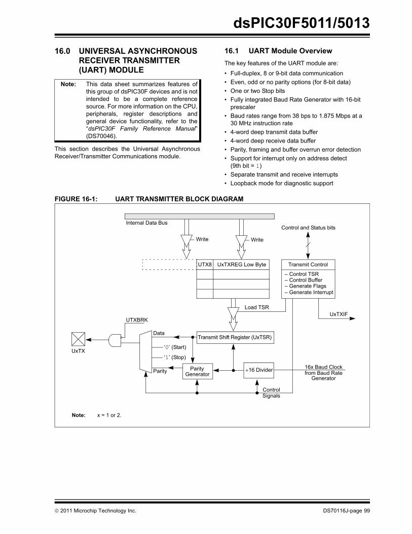
dsPIC30F5011/5013
16.0 UNIVERSAL ASYNCHRONOUS RECEIVER TRANSMITTER (UART) MODULE
This section describes the Universal AsynchronousReceiver/Transmitter Communications module.
16.1 UART Module OverviewThe key features of the UART module are:
• Full-duplex, 8 or 9-bit data communication• Even, odd or no parity options (for 8-bit data)• One or two Stop bits• Fully integrated Baud Rate Generator with 16-bit
prescaler• Baud rates range from 38 bps to 1.875 Mbps at a
30 MHz instruction rate• 4-word deep transmit data buffer• 4-word deep receive data buffer• Parity, framing and buffer overrun error detection• Support for interrupt only on address detect
(9th bit = 1)• Separate transmit and receive interrupts• Loopback mode for diagnostic support
FIGURE 16-1: UART TRANSMITTER BLOCK DIAGRAM
Note: This data sheet summarizes features ofthis group of dsPIC30F devices and is notintended to be a complete referencesource. For more information on the CPU,peripherals, register descriptions andgeneral device functionality, refer to the“dsPIC30F Family Reference Manual”(DS70046).
Write Write
UTX8 UxTXREG Low Byte
Load TSR
Transmit Control
– Control TSR– Control Buffer– Generate Flags– Generate Interrupt
Control and Status bits
UxTXIF
Data
‘0’ (Start)
‘1’ (Stop)
Parity ParityGenerator
Transmit Shift Register (UxTSR)
16 Divider
ControlSignals
16x Baud Clockfrom Baud Rate
Generator
Internal Data Bus
UTXBRK
UxTX
Note: x = 1 or 2.
© 2011 Microchip Technology Inc. DS70116J-page 99

dsPIC30F5011/5013
FIGURE 16-2: UART RECEIVER BLOCK DIAGRAMRead
URX8 UxRXREG Low Byte
Load RSR
UxMODE
Receive Buffer Control– Generate Flags– Generate Interrupt
UxRXIF
UxRX
· Start bit Detect
Receive Shift Register
16 Divider
ControlSignals
UxSTA
– Shift Data Characters
Read ReadWrite Write
to Buffer
8-9
(UxRSR) PER
R
FER
R
· Parity Check· Stop bit Detect· Shift Clock Generation· Wake Logic
16Internal Data Bus
1
0
LPBACKFrom UxTX
16x Baud Clock fromBaud Rate Generator
DS70116J-page 100 © 2011 Microchip Technology Inc.

dsPIC30F5011/5013
16.2 Enabling and Setting Up UART16.2.1 ENABLING THE UARTThe UART module is enabled by setting the UARTENbit in the UxMODE register (where x = 1 or 2). Onceenabled, the UxTX and UxRX pins are configured as anoutput and an input respectively, overriding the TRISand LATCH register bit settings for the correspondingI/O port pins. The UxTX pin is at logic ‘1’ when notransmission is taking place.
16.2.2 DISABLING THE UARTThe UART module is disabled by clearing the UARTENbit in the UxMODE register. This is the default stateafter any Reset. If the UART is disabled, all I/O pinsoperate as port pins under the control of the latch andTRIS bits of the corresponding port pins.
Disabling the UART module resets the buffers to emptystates. Any data characters in the buffers are lost andthe baud rate counter is reset.
All error and status flags associated with the UARTmodule are reset when the module is disabled. TheURXDA, OERR, FERR, PERR, UTXEN, UTXBRK andUTXBF bits are cleared, whereas RIDLE and TRMTare set. Other control bits, including ADDEN,URXISEL<1:0>, UTXISEL, as well as the UxMODEand UxBRG registers, are not affected.
Clearing the UARTEN bit while the UART is active willabort all pending transmissions and receptions andreset the module as defined above. Reenabling theUART will restart the UART in the same configuration.
16.2.3 SETTING UP DATA, PARITY AND STOP BIT SELECTIONS
Control bits PDSEL<1:0> in the UxMODE register areused to select the data length and parity used in thetransmission. The data length may either be 8 bits witheven, odd or no parity, or 9 bits with no parity.
The STSEL bit determines whether one or two Stop bitswill be used during data transmission.
The default (power-on) setting of the UART is 8 bits, noparity and 1 Stop bit (typically represented as 8, N, 1).
16.3 Transmitting Data
16.3.1 TRANSMITTING IN 8-BIT DATA MODE
The following steps must be performed in order totransmit 8-bit data:
1. Set up the UART:First, the data length, parity and number of Stopbits must be selected. Then, the transmit andreceive interrupt enable and priority bits aresetup in the UxMODE and UxSTA registers.Also, the appropriate baud rate value must bewritten to the UxBRG register.
2. Enable the UART by setting the UARTEN bit(UxMODE<15>).
3. Set the UTXEN bit (UxSTA<10>), therebyenabling a transmission.
4. Write the byte to be transmitted to the lower byteof UxTXREG. The value will be transferred to theTransmit Shift register (UxTSR) immediatelyand the serial bit stream will start shifting outduring the next rising edge of the baud clock.Alternatively, the data byte may be written whileUTXEN = 0, following which, the user may setUTXEN. This will cause the serial bit stream tobegin immediately because the baud clock willstart from a cleared state.
5. A transmit interrupt will be generated, depend-ing on the value of the interrupt control bitUTXISEL (UxSTA<15>).
16.3.2 TRANSMITTING IN 9-BIT DATA MODE
The sequence of steps involved in the transmission of9-bit data is similar to 8-bit transmission, except that a16-bit data word (of which the upper 7 bits are alwaysclear) must be written to the UxTXREG register.
16.3.3 TRANSMIT BUFFER (UXTXB)The transmit buffer is 9 bits wide and 4 charactersdeep. Including the Transmit Shift register (UxTSR),the user effectively has a 5-deep FIFO (First-In, First-Out) buffer. The UTXBF Status bit (UxSTA<9>)indicates whether the transmit buffer is full.
If a user attempts to write to a full buffer, the new datawill not be accepted into the FIFO, and no data shift willoccur within the buffer. This enables recovery from abuffer overrun condition.
The FIFO is reset during any device Reset but is notaffected when the device enters or wakes up from aPower-Saving mode.
© 2011 Microchip Technology Inc. DS70116J-page 101

dsPIC30F5011/5013
16.3.4 TRANSMIT INTERRUPTThe transmit interrupt flag (U1TXIF or U2TXIF) islocated in the corresponding interrupt flag register.The transmitter generates an edge to set the UxTXIFbit. The condition for generating the interrupt dependson the UTXISEL control bit:
a) If UTXISEL = 0, an interrupt is generated whena word is transferred from the transmit buffer tothe Transmit Shift register (UxTSR). This impliesthat the transmit buffer has at least one emptyword.
b) If UTXISEL = 1, an interrupt is generated whena word is transferred from the transmit buffer tothe Transmit Shift register (UxTSR) and thetransmit buffer is empty.
Switching between the two Interrupt modes duringoperation is possible and sometimes offers moreflexibility.
16.3.5 TRANSMIT BREAKSetting the UTXBRK bit (UxSTA<11>) will cause theUxTX line to be driven to logic ‘0’. The UTXBRK bitoverrides all transmission activity. Therefore, the usershould generally wait for the transmitter to be Idlebefore setting UTXBRK.
To send a break character, the UTXBRK bit must be setby software and must remain set for a minimum of 13baud clock cycles. The UTXBRK bit is then cleared bysoftware to generate Stop bits. The user must wait for aduration of at least one or two baud clock cycles in orderto ensure a valid Stop bit(s) before reloading the UxTXB,or starting other transmitter activity. Transmission of abreak character does not generate a transmit interrupt.
16.4 Receiving Data
16.4.1 RECEIVING IN 8-BIT OR 9-BIT DATA MODE
The following steps must be performed while receiving8-bit or 9-bit data:
1. Set up the UART (see Section 16.3.1“Transmitting in 8-bit data mode”).
2. Enable the UART (see Section 16.3.1“Transmitting in 8-bit data mode”).
3. A receive interrupt will be generated when oneor more data words have been received,depending on the receive interrupt settingsspecified by the URXISEL bits (UxSTA<7:6>).
4. Read the OERR bit to determine if an overrunerror has occurred. The OERR bit must be resetin software.
5. Read the received data from UxRXREG. The actof reading UxRXREG will move the next word tothe top of the receive FIFO, and the PERR andFERR values will be updated.
16.4.2 RECEIVE BUFFER (UXRXB)The receive buffer is 4 words deep. Including theReceive Shift register (UxRSR), the user effectivelyhas a 5-word deep FIFO buffer.
URXDA (UxSTA<0>) = 1 indicates that the receive buf-fer has data available. URXDA = 0 implies that the buf-fer is empty. If a user attempts to read an empty buffer,the old values in the buffer will be read and no data shiftwill occur within the FIFO.
The FIFO is reset during any device Reset. It is notaffected when the device enters or wakes up from aPower-Saving mode.
16.4.3 RECEIVE INTERRUPTThe receive interrupt flag (U1RXIF or U2RXIF) can beread from the corresponding interrupt flag register. Theinterrupt flag is set by an edge generated by thereceiver. The condition for setting the receive interruptflag depends on the settings specified by theURXISEL<1:0> (UxSTA<7:6>) control bits.
a) If URXISEL<1:0> = 00 or 01, an interrupt is gen-erated every time a data word is transferredfrom the Receive Shift register (UxRSR) to thereceive buffer. There may be one or morecharacters in the receive buffer.
b) If URXISEL<1:0> = 10, an interrupt is generatedwhen a word is transferred from the Receive Shiftregister (UxRSR) to the receive buffer, which as aresult of the transfer, contains 3 characters.
c) If URXISEL<1:0> = 11, an interrupt is set whena word is transferred from the Receive Shift reg-ister (UxRSR) to the receive buffer, which as aresult of the transfer, contains 4 characters (i.e.,becomes full).
Switching between the Interrupt modes during opera-tion is possible, though generally not advisable duringnormal operation.
16.5 Reception Error Handling
16.5.1 RECEIVE BUFFER OVERRUN ERROR (OERR BIT)
The OERR bit (UxSTA<1>) is set if all of the followingconditions occur:
a) The receive buffer is full.b) The Receive Shift register is full, but unable to
transfer the character to the receive buffer.c) The Stop bit of the character in the UxRSR is
detected, indicating that the UxRSR needs totransfer the character to the buffer.
Once OERR is set, no further data is shifted in UxRSR(until the OERR bit is cleared in software or a Resetoccurs). The data held in UxRSR and UxRXREGremains valid.
DS70116J-page 102 © 2011 Microchip Technology Inc.

dsPIC30F5011/5013
16.5.2 FRAMING ERROR (FERR)The FERR bit (UxSTA<2>) is set if a ‘0’ is detectedinstead of a Stop bit. If two Stop bits are selected, bothStop bits must be ‘1’, otherwise FERR will be set. Theread-only FERR bit is buffered along with the receiveddata. It is cleared on any Reset.16.5.3 PARITY ERROR (PERR)The PERR bit (UxSTA<3>) is set if the parity of thereceived word is incorrect. This error bit is applicableonly if a Parity mode (odd or even) is selected. Theread-only PERR bit is buffered along with the receiveddata bytes. It is cleared on any Reset.
16.5.4 IDLE STATUSWhen the receiver is active (i.e., between the initialdetection of the Start bit and the completion of the Stopbit), the RIDLE bit (UxSTA<4>) is ‘0’. Between the com-pletion of the Stop bit and detection of the next Start bit,the RIDLE bit is ‘1’, indicating that the UART is Idle.
16.5.5 RECEIVE BREAKThe receiver will count and expect a certain number ofbit times based on the values programmed in thePDSEL (UxMODE<2:1>) and STSEL (UxMODE<0>)bits.
If the break is longer than 13 bit times, the reception isconsidered complete after the number of bit timesspecified by PDSEL and STSEL. The URXDA bit is set,FERR is set, zeros are loaded into the receive FIFO,interrupts are generated if appropriate and the RIDLEbit is set.
When the module receives a long break signal and thereceiver has detected the Start bit, the data bits and theinvalid Stop bit (which sets the FERR), the receivermust wait for a valid Stop bit before looking for the nextStart bit. It cannot assume that the break condition onthe line is the next Start bit.
Break is regarded as a character containing all ‘0’s withthe FERR bit set. The break character is loaded into thebuffer. No further reception can occur until a Stop bit isreceived. Note that RIDLE goes high when the Stop bithas not yet been received.
16.6 Address Detect ModeSetting the ADDEN bit (UxSTA<5>) enables this spe-cial mode in which a 9th bit (URX8) value of ‘1’ identi-fies the received word as an address, rather than data.This mode is only applicable for 9-bit data communica-tion. The URXISEL control bit does not have anyimpact on interrupt generation in this mode since aninterrupt (if enabled) will be generated every time thereceived word has the 9th bit set.
16.7 Loopback ModeSetting the LPBACK bit enables this special mode inwhich the UxTX pin is internally connected to the UxRXpin. When configured for the Loopback mode, theUxRX pin is disconnected from the internal UARTreceive logic. However, the UxTX pin still functions asin a normal operation.
To select this mode:
1. Configure UART for desired mode of operation.2. Set LPBACK = 1 to enable Loopback mode.3. Enable transmission as defined in Section 16.3
“Transmitting Data”.
16.8 Baud Rate GeneratorThe UART has a 16-bit Baud Rate Generator to allowmaximum flexibility in baud rate generation. The BaudRate Generator register (UxBRG) is readable andwritable. The baud rate is computed as follows:
BRG = 16-bit value held in UxBRG register (0 through 65535)
FCY = Instruction Clock Rate (1/TCY)
The Baud Rate is given by Equation 16-1.
EQUATION 16-1: BAUD RATE
Therefore, the maximum baud rate possible is
FCY/16 (if BRG = 0),
and the minimum baud rate possible is
FCY/(16* 65536).
With a full 16-bit Baud Rate Generator at 30 MIPSoperation, the minimum baud rate achievable is28.5 bps.
Baud Rate = FCY/(16*(BRG+1))
© 2011 Microchip Technology Inc. DS70116J-page 103

dsPIC30F5011/5013
16.9 Auto Baud SupportTo allow the system to determine baud rates ofreceived characters, the input can be optionally linkedto a capture input (IC1 for UART1, IC2 for UART2). Toenable this mode, the user must program the input cap-ture module to detect the falling and rising edges of theStart bit.16.10 UART Operation During CPU Sleep and Idle Modes
16.10.1 UART OPERATION DURING CPU SLEEP MODE
When the device enters Sleep mode, all clock sourcesto the module are shutdown and stay at logic ‘0’. If entryinto Sleep mode occurs while a transmission is in prog-ress, then the transmission is aborted. The UxTX pin isdriven to logic ‘1’. Similarly, if entry into Sleep modeoccurs while a reception is in progress, then the recep-tion is aborted. The UxSTA, UxMODE, transmit andreceive registers and buffers, and the UxBRG registerare not affected by Sleep mode.
If the WAKE bit (UxMODE<7>) is set before the deviceenters Sleep mode, then a falling edge on the UxRX pinwill generate a receive interrupt. The Receive InterruptSelect mode bit (URXISEL) has no effect for this func-tion. If the receive interrupt is enabled, then this willwake-up the device from Sleep. The UARTEN bit mustbe set in order to generate a wake-up interrupt.
16.10.2 UART OPERATION DURING CPU IDLE MODE
For the UART, the USIDL bit selects if the module willstop operation when the device enters Idle mode orwhether the module will continue on Idle. If USIDL = 0,the module will continue operation during Idle mode. IfUSIDL = 1, the module will stop on Idle.
DS70116J-page 104 © 2011 Microchip Technology Inc.

dsPIC30F5011/5013
TAB
LE 1
6-1:
UA
RT1
REG
ISTE
R M
AP(1
)
TAB
LE 1
6-2:
UA
RT2
REG
ISTE
R M
AP(1
)
SFR
Nam
eA
ddr.
Bit
15B
it 14
Bit
13B
it 12
Bit
11B
it 10
Bit
9B
it 8
Bit
7B
it 6
Bit
5B
it 4
Bit
3B
it 2
Bit
1B
it 0
Res
et S
tate
U1M
OD
E02
0CU
AR
TEN
—U
SID
L—
——
——
WA
KE
LPB
ACK
ABA
UD
——
PD
SEL1
PD
SEL0
STS
EL
0000 0000 0000 0000
U1S
TA02
0EU
TXIS
EL—
——
UTX
BRK
UTX
EN
UTX
BF
TRM
TU
RX
ISEL
1U
RX
ISE
L0A
DD
EN
RID
LEPE
RR
FER
RO
ERR
UR
XDA
0000 0001 0001 0000
U1T
XR
EG
0210
——
——
——
—U
TX8
Tran
smit
Reg
iste
r0000 000u uuuu uuuu
U1R
XR
EG
0212
——
——
——
—U
RX
8R
ecei
ve R
egis
ter
0000 0000 0000 0000
U1B
RG
0214
Bau
d R
ate
Gen
erat
or P
resc
aler
0000 0000 0000 0000
Lege
nd:
u =
uni
nitia
lized
bit;
— =
uni
mpl
emen
ted,
read
as
‘0’
Not
e1:
Ref
er to
the
“dsP
IC30
F Fa
mily
Ref
eren
ce M
anua
l” (D
S70
046)
for d
escr
iptio
ns o
f reg
iste
r bit
field
s.
SFR
N
ame
Add
r.B
it 15
Bit
14B
it 13
Bit
12B
it 11
Bit
10B
it 9
Bit
8B
it 7
Bit
6B
it 5
Bit
4B
it 3
Bit
2B
it 1
Bit
0R
eset
Sta
te
U2M
OD
E02
16U
AR
TEN
—U
SID
L—
——
——
WAK
ELP
BAC
KA
BAU
D—
—P
DSE
L1P
DSE
L0ST
SE
L0000 0000 0000 0000
U2S
TA02
18U
TXIS
EL
——
—U
TXB
RK
UTX
EN
UTX
BF
TRM
TU
RX
ISEL
1U
RXI
SEL0
ADD
ENR
IDLE
PER
RFE
RR
OER
RU
RX
DA
0000 0001 0001 0000
U2T
XR
EG
021A
——
——
——
—U
TX8
Tran
smit
Reg
iste
r0000 000u uuuu uuuu
U2R
XR
EG
021C
——
——
——
—U
RX8
Rec
eive
Reg
iste
r0000 0000 0000 0000
U2B
RG
021E
Baud
Rat
e G
ener
ator
Pre
scal
er0000 0000 0000 0000
Lege
nd:
u =
uni
nitia
lized
bit;
— =
uni
mpl
emen
ted,
read
as
‘0’
Not
e1:
Ref
er to
the
“dsP
IC30
F Fa
mily
Ref
eren
ce M
anua
l” (D
S70
046)
for d
escr
iptio
ns o
f reg
iste
r bit
field
s.
© 2011 Microchip Technology Inc. DS70116J-page 105

dsPIC30F5011/5013
NOTES:DS70116J-page 106 © 2011 Microchip Technology Inc.

dsPIC30F5011/5013
17.0 CAN MODULE
17.1 Overview The Controller Area Network (CAN) module is a serialinterface, useful for communicating with other CANmodules or microcontroller devices. This interface/protocol was designed to allow communications withinnoisy environments. The CAN module is a communication controller imple-menting the CAN 2.0 A/B protocol, as defined in theBOSCH specification. The module will support CAN 1.2,CAN 2.0A, CAN 2.0B Passive and CAN 2.0B Active ver-sions of the protocol. The module implementation is afull CAN system. The CAN specification is not coveredwithin this data sheet. The reader may refer to theBOSCH CAN specification for further details.The module features are as follows:• Implementation of the CAN protocol CAN 1.2,
CAN 2.0A and CAN 2.0B • Standard and extended data frames• 0-8 bytes data length• Programmable bit rate up to 1 Mbps• Support for remote frames• Double-buffered receiver with two prioritized
received message storage buffers (each buffer may contain up to 8 bytes of data)
• 6 full (standard/extended identifier) acceptance filters, 2 associated with the high priority receive buffer and 4 associated with the low priority receive buffer
• 2 full acceptance filter masks, one each associated with the high and low priority receive buffers
• Three transmit buffers with application specified prioritization and abort capability (each buffer may contain up to 8 bytes of data)
• Programmable wake-up functionality with integrated low-pass filter
• Programmable Loopback mode supports self-test operation
• Signaling via interrupt capabilities for all CAN receiver and transmitter error states
• Programmable clock source• Programmable link to Input Capture module (IC2,
for both CAN1 and CAN2) for time-stamping and network synchronization
• Low-power Sleep and Idle mode
The CAN bus module consists of a protocol engine andmessage buffering/control. The CAN protocol enginehandles all functions for receiving and transmittingmessages on the CAN bus. Messages are transmittedby first loading the appropriate data registers. Statusand errors can be checked by reading the appropriateregisters. Any message detected on the CAN bus ischecked for errors and then matched against filters tosee if it should be received and stored in one of thereceive registers.
17.2 Frame TypesThe CAN module transmits various types of frameswhich include data messages or remote transmissionrequests initiated by the user, as other frames that areautomatically generated for control purposes. Thefollowing frame types are supported:
• Standard Data Frame:A standard data frame is generated by a nodewhen the node wishes to transmit data. It includesan 11-bit standard identifier (SID), but not an 18-bitextended identifier (EID).
• Extended Data Frame:An extended data frame is similar to a standarddata frame but includes an extended identifier aswell.
• Remote Frame:It is possible for a destination node to request thedata from the source. For this purpose, the desti-nation node sends a remote frame with an identi-fier that matches the identifier of the required dataframe. The appropriate data source node will thensend a data frame as a response to this remoterequest.
• Error Frame:An error frame is generated by any node thatdetects a bus error. An error frame consists of 2fields: an error flag field and an error delimiterfield.
• Overload Frame: An overload frame can be generated by a node asa result of 2 conditions. First, the node detects adominant bit during interframe space which is anillegal condition. Second, due to internal condi-tions, the node is not yet able to start reception ofthe next message. A node may generate a maxi-mum of 2 sequential overload frames to delay thestart of the next message.
• Interframe Space:Interframe space separates a proceeding frame(of whatever type) from a following data or remoteframe.
Note: This data sheet summarizes features ofthis group of dsPIC30F devices and is notintended to be a complete referencesource. For more information on the CPU,peripherals, register descriptions andgeneral device functionality, refer to the“dsPIC30F Family Reference Manual”(DS70046).
© 2011 Microchip Technology Inc. DS70116J-page 107

dsPIC30F5011/5013
FIGURE 17-1: CAN BUFFERS AND PROTOCOL ENGINE BLOCK DIAGRAMAcceptance FilterRXF2
RXB1
Accept
Accept
Identifier
Data Field Data Field
Identifier
Acceptance MaskRXM1
Acceptance FilterRXF3
Acceptance FilterRXF4
Acceptance FilterRXF5
MAB
Acceptance MaskRXM0
Acceptance FilterRXF0
Acceptance FilterRXF1
RXB0
MS
GR
EQ
TXB2
TXA
BT
TXLA
RB
TXE
RR
MTX
BUFF
MES
SAG
E
MessageQueueControl
Transmit Byte Sequencer
MS
GR
EQTXB1
TXA
BT
TXLA
RB
TXE
RR
MTX
BUFF
MES
SAG
E
MS
GR
EQ
TXB0
TXA
BT
TXLA
RB
TXE
RR
MTX
BUFF
MES
SAG
E
Receive ShiftTransmit Shift
ReceiveError
TransmitError
Protocol
RERRCNT
TERRCNT
Err PasBus Off
FiniteState
Machine
Counter
Counter
TransmitLogic
BitTimingLogic
CiTX(1) CiRX(1)
Bit TimingGenerator
PROTOCOLENGINE
BUFFERS
CRC CheckCRC Generator
Note 1: i = 1 or 2 refers to a particular CAN module (CAN1 or CAN2).
DS70116J-page 108 © 2011 Microchip Technology Inc.

dsPIC30F5011/5013
17.3 Modes of OperationThe CAN module can operate in one of several operationmodes selected by the user. These modes include:• Initialization Mode• Disable Mode• Normal Operation Mode• Listen Only Mode• Loopback Mode• Error Recognition ModeModes are requested by setting the REQOP<2:0> bits(CiCTRL<10:8>). Entry into a mode is Acknowledgedby monitoring the OPMODE<2:0> bits (CiCTRL<7:5>).The module will not change the mode and theOPMODE bits until a change in mode is acceptable,generally during bus Idle time which is defined as atleast 11 consecutive recessive bits.
17.3.1 INITIALIZATION MODEIn the Initialization mode, the module will not transmit orreceive. The error counters are cleared and the inter-rupt flags remain unchanged. The programmer willhave access to configuration registers that are accessrestricted in other modes. The module will protect theuser from accidentally violating the CAN protocolthrough programming errors. All registers which controlthe configuration of the module can not be modifiedwhile the module is on-line. The CAN module will notbe allowed to enter the Configuration mode while atransmission is taking place. The Configuration modeserves as a lock to protect the following registers.• All Module Control Registers• Baud Rate and Interrupt Configuration Registers • Bus Timing Registers • Identifier Acceptance Filter Registers • Identifier Acceptance Mask Registers
17.3.2 DISABLE MODEIn Disable mode, the module will not transmit orreceive. The module has the ability to set the WAKIF bitdue to bus activity, however, any pending interrupts willremain and the error counters will retain their value.
If the REQOP<2:0> bits (CiCTRL<10:8>) = 001, themodule will enter the Module Disable mode. If the moduleis active, the module will wait for 11 recessive bits on theCAN bus, detect that condition as an Idle bus, thenaccept the module disable command. When theOPMODE<2:0> bits (CiCTRL<7:5>) = 001, that indi-cates whether the module successfully went into ModuleDisable mode. The I/O pins will revert to normal I/Ofunction when the module is in the Module Disable mode.
The module can be programmed to apply a low-passfilter function to the CiRX input line while the module orthe CPU is in Sleep mode. The WAKFIL bit(CiCFG2<14>) enables or disables the filter.
17.3.3 NORMAL OPERATION MODENormal operating mode is selected whenREQOP<2:0> = 000. In this mode, the module is acti-vated and the I/O pins assume the CAN bus functions.The module transmits and receives CAN bus mes-sages via the CxTX and CxRX pins.
17.3.4 LISTEN ONLY MODEIf the Listen Only mode is activated, the module on theCAN bus is passive. The transmitter buffers revert tothe port I/O function. The receive pins remain inputs.For the receiver, no error flags or Acknowledge signalsare sent. The error counters are deactivated in thisstate. The Listen Only mode can be used for detectingthe baud rate on the CAN bus. To use this, it is neces-sary that there are at least two further nodes thatcommunicate with each other.
17.3.5 LISTEN ALL MESSAGES MODEThe module can be set to ignore all errors and receiveany message. The Listen All Messages mode is acti-vated by setting the REQOP<2:0> bits to ‘111’. In thismode, the data which is in the message assembly buf-fer until the time an error occurred, is copied in thereceive buffer and can be read via the CPU interface.
17.3.6 LOOPBACK MODEIf the Loopback mode is activated, the module con-nects the internal transmit signal to the internal receivesignal at the module boundary. The transmit andreceive pins revert to their port I/O function.
Note: Typically, if the CAN module is allowed totransmit in a particular mode of operationand a transmission is requested immedi-ately after the CAN module has beenplaced in that mode of operation, the mod-ule waits for 11 consecutive recessive bitson the bus before starting transmission. Ifthe user switches to Disable mode withinthis 11-bit period, then this transmission isaborted and the corresponding TXABT bitis set and TXREQ bit is cleared.
© 2011 Microchip Technology Inc. DS70116J-page 109

dsPIC30F5011/5013
17.4 Message Reception17.4.1 RECEIVE BUFFERSThe CAN bus module has 3 receive buffers. However,one of the receive buffers is always committed to mon-itoring the bus for incoming messages. This buffer iscalled the Message Assembly Buffer (MAB). There are2 receive buffers visible, RXB0 and RXB1, that canessentially instantaneously receive a completemessage from the protocol engine.
All messages are assembled by the MAB and are trans-ferred to the RXBn buffers only if the acceptance filtercriterion are met. When a message is received, theRXnIF flag (CiINTF<0> or CiINRF<1>) will be set. Thisbit can only be set by the module when a message isreceived. The bit is cleared by the CPU when it has com-pleted processing the message in the buffer. If theRXnIE bit (CiINTE<0> or CiINTE<1>) is set, an interruptwill be generated when a message is received.
RXF0 and RXF1 filters with RXM0 mask are associatedwith RXB0. The filters RXF2, RXF3, RXF4, and RXF5and the mask RXM1 are associated with RXB1.
17.4.2 MESSAGE ACCEPTANCE FILTERSThe message acceptance filters and masks are used todetermine if a message in the message assembly buf-fer should be loaded into either of the receive buffers.Once a valid message has been received into the MAB,the identifier fields of the message are compared to thefilter values. If there is a match, that message will beloaded into the appropriate receive buffer.
The acceptance filter looks at incoming messages forthe RXIDE bit (CiRXnSID<0>) to determine how tocompare the identifiers. If the RXIDE bit is clear, themessage is a standard frame and only filters with theEXIDE bit (CiRXFnSID<0>) clear are compared. If theRXIDE bit is set, the message is an extended frame,and only filters with the EXIDE bit set are compared.Configuring the RXM<1:0> bits to ‘01’ or ‘10’ canoverride the EXIDE bit.
17.4.3 MESSAGE ACCEPTANCE FILTER MASKS
The mask bits essentially determine which bits to applythe filter to. If any mask bit is set to a zero, then that bitwill automatically be accepted regardless of the filterbit. There are 2 programmable acceptance filter masksassociated with the receive buffers, one for each buffer.
17.4.4 RECEIVE OVERRUNAn overrun condition occurs when the MAB hasassembled a valid received message, the message isaccepted through the acceptance filters and when thereceive buffer associated with the filter has not beendesignated as clear of the previous message.
The overrun error flag, RXnOVR (CiINTF<15> orCiINTF<14>), and the ERRIF bit (CiINTF<5>) will beset and the message in the MAB will be discarded.
If the DBEN bit is clear, RXB1 and RXB0 operate inde-pendently. When this is the case, a message intendedfor RXB0 will not be diverted into RXB1 if RXB0 con-tains an unread message and the RX0OVR bit will beset.
If the DBEN bit is set, the overrun for RXB0 is handleddifferently. If a valid message is received for RXB0 andRXFUL = 1 indicates that RXB0 is full and RXFUL = 0indicates that RXB1 is empty, the message for RXB0will be loaded into RXB1. An overrun error will not begenerated for RXB0. If a valid message is received forRXB0 and RXFUL = 1, indicating that both RXB0 andRXB1 are full, the message will be lost and an overrunwill be indicated for RXB1.
17.4.5 RECEIVE ERRORSThe CAN module will detect the following receiveerrors:
• Cyclic Redundancy Check (CRC) Error• Bit Stuffing Error• Invalid Message Receive Error
The receive error counter is incremented by one incase one of these errors occur. The RXWAR bit(CiINTF<9>) indicates that the receive error counterhas reached the CPU warning limit of 96 and aninterrupt is generated.
17.4.6 RECEIVE INTERRUPTSReceive interrupts can be divided into 3 major groups,each including various conditions that generateinterrupts:
• Receive Interrupt:A message has been successfully received andloaded into one of the receive buffers. This inter-rupt is activated immediately after receiving theEnd-of-Frame (EOF) field. Reading the RXnIF flagwill indicate which receive buffer caused theinterrupt.
• Wake-up Interrupt:The CAN module has woken up from Disablemode or the device has woken up from Sleepmode.
DS70116J-page 110 © 2011 Microchip Technology Inc.

dsPIC30F5011/5013
• Receive Error Interrupts:A receive error interrupt will be indicated by theERRIF bit. This bit shows that an error conditionoccurred. The source of the error can be deter-mined by checking the bits in the CAN InterruptStatus register, CiINTF.
- Invalid Message Received:If any type of error occurred during reception ofthe last message, an error will be indicated bythe IVRIF bit.
- Receiver Overrun:The RXnOVR bit indicates that an overruncondition occurred.
- Receiver Warning: The RXWAR bit indicates that the receive errorcounter (RERRCNT<7:0>) has reached thewarning limit of 96.
- Receiver Error Passive:The RXEP bit indicates that the receive errorcounter has exceeded the error passive limit of127 and the module has gone into error passivestate.
17.5 Message Transmission
17.5.1 TRANSMIT BUFFERSThe CAN module has three transmit buffers. Each ofthe three buffers occupies 14 bytes of data. Eight of thebytes are the maximum 8 bytes of the transmitted mes-sage. Five bytes hold the standard and extendedidentifiers and other message arbitration information.
17.5.2 TRANSMIT MESSAGE PRIORITYTransmit priority is a prioritization within each node ofthe pending transmittable messages. There are4 levels of transmit priority. If TXPRI<1:0>(CiTXnCON<1:0>, where n = 0, 1 or 2 represents a par-ticular transmit buffer) for a particular message buffer isset to ‘11’, that buffer has the highest priority. IfTXPRI<1:0> for a particular message buffer is set to‘10’ or ‘01’, that buffer has an intermediate priority. IfTXPRI<1:0> for a particular message buffer is ‘00’, thatbuffer has the lowest priority.
17.5.3 TRANSMISSION SEQUENCETo initiate transmission of the message, the TXREQ bit(CiTXnCON<3>) must be set. The CAN bus moduleresolves any timing conflicts between setting of theTXREQ bit and the Start-of-Frame (SOF), ensuring that ifthe priority was changed, it is resolved correctly before theSOF occurs. When TXREQ is set, the TXABT(CiTXnCON<6>), TXLARB (CiTXnCON<5>) and TXERR(CiTXnCON<4>) flag bits are automatically cleared.
Setting TXREQ bit simply flags a message buffer asenqueued for transmission. When the module detectsan available bus, it begins transmitting the messagewhich has been determined to have the highest priority.
If the transmission completes successfully on the firstattempt, the TXREQ bit is cleared automatically, and aninterrupt is generated if TXIE was set.
If the message transmission fails, one of the error con-dition flags will be set, and the TXREQ bit will remainset indicating that the message is still pending for trans-mission. If the message encountered an error conditionduring the transmission attempt, the TXERR bit will beset, and the error condition may cause an interrupt. Ifthe message loses arbitration during the transmissionattempt, the TXLARB bit is set. No interrupt isgenerated to signal the loss of arbitration.
17.5.4 ABORTING MESSAGE TRANSMISSION
The system can also abort a message by clearing theTXREQ bit associated with each message buffer. Set-ting the ABAT bit (CiCTRL<12>) will request an abort ofall pending messages. If the message has not yetstarted transmission, or if the message started but isinterrupted by loss of arbitration or an error, the abortwill be processed. The abort is indicated when themodule sets the TXABT bit and the TXnIF flag is notautomatically set.
17.5.5 TRANSMISSION ERRORSThe CAN module will detect the following transmissionerrors:
• Acknowledge Error• Form Error• Bit Error
These transmission errors will not necessarily generatean interrupt but are indicated by the transmission errorcounter. However, each of these errors will cause thetransmission error counter to be incremented by one.Once the value of the error counter exceeds the valueof 96, the ERRIF bit (CiINTF<5>) and the TXWAR bit(CiINTF<10>) are set. Once the value of the errorcounter exceeds the value of 96, an interrupt isgenerated and the TXWAR bit in the Error Flag registeris set.
© 2011 Microchip Technology Inc. DS70116J-page 111

dsPIC30F5011/5013
17.5.6 TRANSMIT INTERRUPTSTransmit interrupts can be divided into 2 major groups,each including various conditions that generateinterrupts:• Transmit Interrupt:At least one of the three transmit buffers is empty(not scheduled) and can be loaded to schedule amessage for transmission. Reading the TXnIFflags will indicate which transmit buffer is availableand caused the interrupt.
• Transmit Error Interrupts:A transmission error interrupt will be indicated bythe ERRIF flag. This flag shows that an error con-dition occurred. The source of the error can bedetermined by checking the error flags in the CANInterrupt Status register, CiINTF. The flags in thisregister are related to receive and transmit errors.
- Transmitter Warning Interrupt:The TXWAR bit indicates that the transmit errorcounter has reached the CPU warning limit of96.
- Transmitter Error Passive:The TXEP bit (CiINTF<12>) indicates that thetransmit error counter has exceeded the errorpassive limit of 127 and the module has gone toerror passive state.
- Bus Off: The TXBO bit (CiINTF<13>) indicates that thetransmit error counter has exceeded 255 andthe module has gone to the bus off state.
17.6 Baud Rate SettingAll nodes on any particular CAN bus must have thesame nominal bit rate. In order to set the baud rate, thefollowing parameters have to be initialized:
• Synchronization Jump Width• Baud Rate Prescaler • Phase Segments• Length determination of Phase Segment 2 • Sample Point • Propagation Segment bits
17.6.1 BIT TIMINGAll controllers on the CAN bus must have the samebaud rate and bit length. However, different controllersare not required to have the same master oscillatorclock. At different clock frequencies of the individualcontrollers, the baud rate has to be adjusted byadjusting the number of time quanta in each segment.
The nominal bit time can be thought of as being dividedinto separate non-overlapping time segments. Thesesegments are shown in Figure 17-2.
• Synchronization Segment (Sync Seg)• Propagation Time Segment (Prop Seg)• Phase Segment 1 (Phase1 Seg)• Phase Segment 2 (Phase2 Seg)
The time segments and also the nominal bit time aremade up of integer units of time called time quanta orTQ. By definition, the nominal bit time has a minimumof 8 TQ and a maximum of 25 TQ. Also, by definition,the minimum nominal bit time is 1 μsec correspondingto a maximum bit rate of 1 MHz.
FIGURE 17-2: CAN BIT TIMING
Input Signal
SyncProp
SegmentPhase
Segment 1Phase
Segment 2 Sync
Sample Point
TQ
DS70116J-page 112 © 2011 Microchip Technology Inc.

dsPIC30F5011/5013
17.6.2 PRESCALER SETTINGThere is a programmable prescaler with integral valuesranging from 1 to 64, in addition to a fixed divide-by-2for clock generation. The time quantum (TQ) is a fixedunit of time derived from the oscillator period, and isgiven by Equation 17-1, where FCAN is FCY (if theCANCKS bit is set) or 4FCY (if CANCKS is clear).EQUATION 17-1: TIME QUANTUM FOR CLOCK GENERATION
17.6.3 PROPAGATION SEGMENT This part of the bit time is used to compensate physicaldelay times within the network. These delay times con-sist of the signal propagation time on the bus line andthe internal delay time of the nodes. The Prop Seg canbe programmed from 1 TQ to 8 TQ by setting thePRSEG<2:0> bits (CiCFG2<2:0>).
17.6.4 PHASE SEGMENTSThe phase segments are used to optimally locate thesampling of the received bit within the transmitted bittime. The sampling point is between Phase1 Seg andPhase2 Seg. These segments are lengthened or short-ened by resynchronization. The end of the Phase1 Segdetermines the sampling point within a bit period. Thesegment is programmable from 1 TQ to 8 TQ. Phase2Seg provides delay to the next transmitted data transi-tion. The segment is programmable from 1 TQ to 8 TQ,or it may be defined to be equal to the greater ofPhase1 Seg or the information processing time (2 TQ).The Phase1 Seg is initialized by setting bitsSEG1PH<2:0> (CiCFG2<5:3>), and Phase2 Seg isinitialized by setting SEG2PH<2:0> (CiCFG2<10:8>).
The following requirement must be fulfilled while settingthe lengths of the phase segments:
Prop Seg + Phase1 Seg > = Phase2 Seg
17.6.5 SAMPLE POINTThe sample point is the point of time at which the buslevel is read and interpreted as the value of that respec-tive bit. The location is at the end of Phase1 Seg. If thebit timing is slow and contains many TQ, it is possible tospecify multiple sampling of the bus line at the samplepoint. The level determined by the CAN bus then corre-sponds to the result from the majority decision of threevalues. The majority samples are taken at the samplepoint and twice before with a distance of TQ/2. TheCAN module allows the user to choose between sam-pling three times at the same point or once at the samepoint, by setting or clearing the SAM bit (CiCFG2<6>).
Typically, the sampling of the bit should take place atabout 60-70% through the bit time, depending on thesystem parameters.
17.6.6 SYNCHRONIZATIONTo compensate for phase shifts between the oscillatorfrequencies of the different bus stations, each CANcontroller must be able to synchronize to the relevantsignal edge of the incoming signal. When an edge inthe transmitted data is detected, the logic will comparethe location of the edge to the expected time (Synchro-nous Segment). The circuit will then adjust the valuesof Phase1 Seg and Phase2 Seg. There are 2mechanisms used to synchronize.
17.6.6.1 Hard SynchronizationHard synchronization is only done whenever there is a‘recessive’ to ‘dominant’ edge during bus Idle indicatingthe start of a message. After hard synchronization, thebit time counters are restarted with the Sync Seg. Hardsynchronization forces the edge which has caused thehard synchronization to lie within the synchronizationsegment of the restarted bit time. If a hard synchroniza-tion is done, there will not be a resynchronization withinthat bit time.
17.6.6.2 ResynchronizationAs a result of resynchronization, Phase1 Seg may belengthened or Phase2 Seg may be shortened. Theamount of lengthening or shortening of the phase buf-fer segment has an upper bound known as the syn-chronization jump width, and is specified by theSJW<1:0> bits (CiCFG1<7:6>). The value of the syn-chronization jump width will be added to Phase1 Seg orsubtracted from Phase2 Seg. The resynchronizationjump width is programmable between 1 TQ and 4 TQ.
The following requirement must be fulfilled while settingthe SJW<1:0> bits:
Phase2 Seg > Synchronization Jump Width
Note: FCAN must not exceed 30 MHz. IfCANCKS = 0, then FCY must not exceed7.5 MHz.
TQ = 2 (BRP<5:0> + 1) / FCAN
© 2011 Microchip Technology Inc. DS70116J-page 113

dsPIC30F5011/5013
TABLE
17-
1:C
AN
1 R
EGIS
TER
MA
P(1)
SFR
Nam
eA
ddr.
Bit
15B
it 14
Bit
13B
it 12
Bit
11B
it 10
Bit
9B
it 8
Bit
7B
it 6
Bit
5B
it 4
Bit
3B
it 2
Bit
1B
it 0
Res
et S
tate
C1R
XF0
SID
0300
——
—R
ecei
ve A
ccep
tanc
e Fi
lter 0
Sta
ndar
d Id
entif
ier <
10:0
>—
EX
IDE
000u uuuu uuuu uu0u
C1R
XF0E
IDH
0302
——
——
Rec
eive
Acc
epta
nce
Filte
r 0 E
xten
ded
Iden
tifie
r <17
:6>
0000 uuuu uuuu uuuu
C1R
XF0E
IDL
0304
Rec
eive
Acc
epta
nce
Filte
r 0 E
xten
ded
Iden
tifie
r <5:
0>—
——
——
——
——
—uuuu uu00 0000 0000
C1R
XF1S
ID03
08—
——
Rec
eive
Acc
epta
nce
Filte
r 1 S
tand
ard
Iden
tifie
r <10
:0>
—E
XID
E000u uuuu uuuu uu0u
C1R
XF1E
IDH
030A
——
——
Rec
eive
Acc
epta
nce
Filte
r 1 E
xten
ded
Iden
tifie
r <17
:6>
0000 uuuu uuuu uuuu
C1R
XF1E
IDL
030C
Rec
eive
Acc
epta
nce
Filte
r 1 E
xten
ded
Iden
tifie
r <5:
0>—
——
——
——
——
—uuuu uu00 0000 0000
C1R
XF2S
ID03
10—
——
Rec
eive
Acc
epta
nce
Filte
r 2 S
tand
ard
Iden
tifie
r <10
:0>
—E
XID
E000u uuuu uuuu uu0u
C1R
XF2E
IDH
0312
——
——
Rec
eive
Acc
epta
nce
Filte
r 2 E
xten
ded
Iden
tifie
r <17
:6>
0000 uuuu uuuu uuuu
C1R
XF2E
IDL
0314
Rec
eive
Acc
epta
nce
Filte
r 2 E
xten
ded
Iden
tifie
r <5:
0>—
——
——
——
——
—uuuu uu00 0000 0000
C1R
XF3S
ID03
18—
——
Rec
eive
Acc
epta
nce
Filte
r 3 S
tand
ard
Iden
tifie
r <10
:0>
—E
XID
E000u uuuu uuuu uu0u
C1R
XF3E
IDH
031A
——
——
Rec
eive
Acc
epta
nce
Filte
r 3 E
xten
ded
Iden
tifie
r <17
:6>
0000 uuuu uuuu uuuu
C1R
XF3E
IDL
031C
Rec
eive
Acc
epta
nce
Filte
r 3 E
xten
ded
Iden
tifie
r <5:
0>—
——
——
——
——
—uuuu uu00 0000 0000
C1R
XF4S
ID03
20—
——
Rec
eive
Acc
epta
nce
Filte
r 4 S
tand
ard
Iden
tifie
r <10
:0>
—E
XID
E000u uuuu uuuu uu0u
C1R
XF4E
IDH
0322
——
——
Rec
eive
Acc
epta
nce
Filte
r 4 E
xten
ded
Iden
tifie
r <17
:6>
0000 uuuu uuuu uuuu
C1R
XF4E
IDL
0324
Rec
eive
Acc
epta
nce
Filte
r 4 E
xten
ded
Iden
tifie
r <5:
0>—
——
——
——
——
—uuuu uu00 0000 0000
C1R
XF5S
ID03
28—
——
Rec
eive
Acc
epta
nce
Filte
r 5 S
tand
ard
Iden
tifie
r <10
:0>
—E
XID
E000u uuuu uuuu uu0u
C1R
XF5E
IDH
032A
——
——
Rec
eive
Acc
epta
nce
Filte
r 5 E
xten
ded
Iden
tifie
r <17
:6>
0000 uuuu uuuu uuuu
C1R
XF5E
IDL
032C
Rec
eive
Acc
epta
nce
Filte
r 5 E
xten
ded
Iden
tifie
r <5:
0>—
——
——
——
——
—uuuu uu00 0000 0000
C1R
XM0S
ID03
30—
——
Rec
eive
Acc
epta
nce
Mas
k 0
Stan
dard
Iden
tifie
r <10
:0>
—M
IDE
000u uuuu uuuu uu0u
C1R
XM0E
IDH
0332
——
——
Rec
eive
Acc
epta
nce
Mas
k 0
Ext
ende
d Id
entif
ier <
17:6
>0000 uuuu uuuu uuuu
C1R
XM0E
IDL
0334
Rec
eive
Acc
epta
nce
Mas
k 0
Exte
nded
Iden
tifie
r <5:
0>—
——
——
——
——
—uuuu uu00 0000 0000
C1R
XM1S
ID03
38—
——
Rec
eive
Acc
epta
nce
Mas
k 1
Stan
dard
Iden
tifie
r <10
:0>
—M
IDE
000u uuuu uuuu uu0u
C1R
XM1E
IDH
033A
——
——
Rec
eive
Acc
epta
nce
Mas
k 1
Ext
ende
d Id
entif
ier <
17:6
>0000 uuuu uuuu uuuu
C1R
XM
1EID
L03
3CR
ecei
ve A
ccep
tanc
e M
ask
1 Ex
tend
ed Id
entif
ier <
5:0>
——
——
——
——
——
uuuu uu00 0000 0000
C1T
X2S
ID03
40Tr
ansm
it B
uffe
r 2 S
tand
ard
Iden
tifie
r <10
:6>
——
—Tr
ansm
it B
uffe
r 2 S
tand
ard
Iden
tifie
r <5:
0>S
RR
TXID
Euuuu u000 uuuu uuuu
C1T
X2E
ID03
42Tr
ansm
it Bu
ffer 2
Ext
ende
d Id
entif
ier<
17:1
4>—
——
—Tr
ansm
it B
uffe
r 2 E
xten
ded
Iden
tifie
r <13
:6>
uuuu 0000 uuuu uuuu
C1T
X2D
LC03
44Tr
ansm
it B
uffe
r 2 E
xten
ded
Iden
tifie
r <5:
0>TX
RTR
TXR
B1
TXR
B0
DLC
<3:0
>—
——
uuuu uuuu uuuu u000
C1T
X2B
103
46Tr
ansm
it Bu
ffer 2
Byt
e 1
Tran
smit
Buf
fer 2
Byt
e 0
uuuu uuuu uuuu uuuu
C1T
X2B
203
48Tr
ansm
it Bu
ffer 2
Byt
e 3
Tran
smit
Buf
fer 2
Byt
e 2
uuuu uuuu uuuu uuuu
C1T
X2B
303
4ATr
ansm
it Bu
ffer 2
Byt
e 5
Tran
smit
Buf
fer 2
Byt
e 4
uuuu uuuu uuuu uuuu
C1T
X2B
403
4CTr
ansm
it Bu
ffer 2
Byt
e 7
Tran
smit
Buf
fer 2
Byt
e 6
uuuu uuuu uuuu uuuu
C1T
X2C
ON
034E
——
——
——
——
—TX
ABT
TXLA
RB
TXE
RR
TXR
EQ
—TX
PR
I<1:
0>0000 0000 0000 0000
C1T
X1S
ID03
50Tr
ansm
it B
uffe
r 1 S
tand
ard
Iden
tifie
r <10
:6>
——
—Tr
ansm
it B
uffe
r 1 S
tand
ard
Iden
tifie
r <5:
0>S
RR
TXID
Euuuu u000 uuuu uuuu
C1T
X1E
ID03
52Tr
ansm
it Bu
ffer 1
Ext
ende
d Id
entif
ier<
17:1
4>—
——
—Tr
ansm
it B
uffe
r 1 E
xten
ded
Iden
tifie
r <13
:6>
uuuu 0000 uuuu uuuu
C1T
X1D
LC03
54Tr
ansm
it B
uffe
r 1 E
xten
ded
Iden
tifie
r <5:
0>TX
RTR
TXR
B1
TXR
B0
DLC
<3:0
>—
——
uuuu uuuu uuuu u000
C1T
X1B
103
56Tr
ansm
it Bu
ffer 1
Byt
e 1
Tran
smit
Buf
fer 1
Byt
e 0
uuuu uuuu uuuu uuuu
Lege
nd:
u =
uni
nitia
lized
bit;
— =
uni
mpl
emen
ted,
read
as
‘0’
Not
e1:
Ref
er to
the
“dsP
IC30
F Fa
mily
Ref
eren
ce M
anua
l” (D
S700
46) f
or d
escr
iptio
ns o
f reg
iste
r bit
field
s.
DS70116J-page 114 © 2011 Microchip Technology Inc.

dsPIC30F5011/5013
C1T
X1B
203
58Tr
ansm
it Bu
ffer 1
Byt
e 3
Tran
smit
Buf
fer 1
Byt
e 2
uuuu uuuu uuuu uuuu
C1T
X1B
303
5ATr
ansm
it Bu
ffer 1
Byt
e 5
Tran
smit
Buf
fer 1
Byt
e 4
uuuu uuuu uuuu uuuu
C1T
X1B
403
5CTr
ansm
it Bu
ffer 1
Byt
e 7
Tran
smit
Buf
fer 1
Byt
e 6
uuuu uuuu uuuu uuuu
C1T
X1C
ON
035E
——
——
——
——
—TX
ABT
TXLA
RB
TXE
RR
TXR
EQ
—TX
PR
I<1:
0>0000 0000 0000 0000
C1T
X0S
ID03
60Tr
ansm
it B
uffe
r 0 S
tand
ard
Iden
tifie
r <10
:6>
——
—Tr
ansm
it B
uffe
r 0 S
tand
ard
Iden
tifie
r <5:
0>S
RR
TXID
Euuuu u000 uuuu uuuu
C1T
X0E
ID03
62Tr
ansm
it Bu
ffer 0
Ext
ende
d Id
entif
ier<
17:1
4>—
——
—Tr
ansm
it B
uffe
r 0 E
xten
ded
Iden
tifie
r <13
:6>
uuuu 0000 uuuu uuuu
C1T
X0D
LC03
64Tr
ansm
it B
uffe
r 0 E
xten
ded
Iden
tifie
r <5:
0>TX
RTR
TXR
B1
TXR
B0
DLC
<3:0
>—
——
uuuu uuuu uuuu u000
C1T
X0B
103
66Tr
ansm
it Bu
ffer 0
Byt
e 1
Tran
smit
Buf
fer 0
Byt
e 0
uuuu uuuu uuuu uuuu
C1T
X0B
203
68Tr
ansm
it Bu
ffer 0
Byt
e 3
Tran
smit
Buf
fer 0
Byt
e 2
uuuu uuuu uuuu uuuu
C1T
X0B
303
6ATr
ansm
it Bu
ffer 0
Byt
e 5
Tran
smit
Buf
fer 0
Byt
e 4
uuuu uuuu uuuu uuuu
C1T
X0B
403
6CTr
ansm
it Bu
ffer 0
Byt
e 7
Tran
smit
Buf
fer 0
Byt
e 6
uuuu uuuu uuuu uuuu
C1T
X0C
ON
036E
——
——
——
——
—TX
ABT
TXLA
RB
TXE
RR
TXR
EQ
—TX
PR
I<1:
0>0000 0000 0000 0000
C1R
X1S
ID03
70—
——
Rec
eive
Buf
fer 1
Sta
ndar
d Id
entif
ier <
10:0
>S
RR
RX
IDE
000u uuuu uuuu uuuu
C1R
X1E
ID03
72—
——
—R
ecei
ve B
uffe
r 1 E
xten
ded
Iden
tifie
r <17
:6>
0000 uuuu uuuu uuuu
C1R
X1D
LC03
74R
ecei
ve B
uffe
r 1 E
xten
ded
Iden
tifie
r <5:
0>R
XR
TRR
XRB1
——
—R
XR
B0D
LC<3
:0>
uuuu uuuu 000u uuuu
C1R
X1B
103
76R
ecei
ve B
uffe
r 1 B
yte
1R
ecei
ve B
uffe
r 1 B
yte
0uuuu uuuu uuuu uuuu
C1R
X1B
203
78R
ecei
ve B
uffe
r 1 B
yte
3R
ecei
ve B
uffe
r 1 B
yte
2uuuu uuuu uuuu uuuu
C1R
X1B
303
7AR
ecei
ve B
uffe
r 1 B
yte
5R
ecei
ve B
uffe
r 1 B
yte
4uuuu uuuu uuuu uuuu
C1R
X1B
403
7CR
ecei
ve B
uffe
r 1 B
yte
7R
ecei
ve B
uffe
r 1 B
yte
6uuuu uuuu uuuu uuuu
C1R
X1C
ON
037E
——
——
——
——
RX
FUL
——
—R
XR
-TR
RO
FILH
IT<2
:0>
0000 0000 0000 0000
C1R
X0S
ID03
80—
——
Rec
eive
Buf
fer 0
Sta
ndar
d Id
entif
ier <
10:0
>S
RR
RX
IDE
000u uuuu uuuu uuuu
C1R
X0E
ID03
82—
——
—R
ecei
ve B
uffe
r 0 E
xten
ded
Iden
tifie
r <17
:6>
0000 uuuu uuuu uuuu
C1R
X0D
LC03
84R
ecei
ve B
uffe
r 0 E
xten
ded
Iden
tifie
r <5:
0>R
XR
TRR
XRB1
——
—R
XR
B0D
LC<3
:0>
uuuu uuuu 000u uuuu
C1R
X0B
103
86R
ecei
ve B
uffe
r 0 B
yte
1R
ecei
ve B
uffe
r 0 B
yte
0uuuu uuuu uuuu uuuu
C1R
X0B
203
88R
ecei
ve B
uffe
r 0 B
yte
3R
ecei
ve B
uffe
r 0 B
yte
2uuuu uuuu uuuu uuuu
C1R
X0B
303
8AR
ecei
ve B
uffe
r 0 B
yte
5R
ecei
ve B
uffe
r 0 B
yte
4uuuu uuuu uuuu uuuu
C1R
X0B
403
8CR
ecei
ve B
uffe
r 0 B
yte
7R
ecei
ve B
uffe
r 0 B
yte
6uuuu uuuu uuuu uuuu
C1R
X0C
ON
038E
——
——
——
——
RX
FUL
——
—R
XR
-TR
RO
DB
EN
JTO
FFFI
LHIT
00000 0000 0000 0000
C1C
TRL
0390
CA
NC
AP
—C
SID
LEAB
ATC
AN
CK
SR
EQ
OP
<2:0
>O
PMO
DE
<2:0
>—
ICO
DE
<2:0
>—
0000 0100 1000 0000
C1C
FG1
0392
——
——
——
——
SJW
<1:0
>B
RP
<5:0
>0000 0000 0000 0000
C1C
FG2
0394
—W
AK
FIL
——
—S
EG
2PH
<2:0
>SE
G2P
HTS
SA
MS
EG
1PH
<2:0
>P
RS
EG
<2:0
>0u00 0uuu uuuu uuuu
C1I
NTF
0396
RX0
OVR
RX
1OV
RTX
BO
TXE
PR
XE
PTX
WAR
RX
WAR
EW
ARN
IVR
IFW
AKI
FE
RR
IFTX
2IF
TX1I
FTX
0IF
RX
1IF
RX
0IF
0000 0000 0000 0000
C1I
NTE
0398
——
——
——
——
IVR
IEW
AKIE
ER
RIE
TX2I
ETX
1IE
TX0I
ER
X1E
RX
0IE
0000 0000 0000 0000
C1E
C03
9ATr
ansm
it Er
ror C
ount
Reg
iste
rR
ecei
ve E
rror C
ount
Reg
iste
r0000 0000 0000 0000
TAB
LE 1
7-1:
CA
N1
REG
ISTE
R M
AP(1
) (C
ON
TIN
UED
)SF
R N
ame
Add
r.B
it 15
Bit
14B
it 13
Bit
12B
it 11
Bit
10B
it 9
Bit
8B
it 7
Bit
6B
it 5
Bit
4B
it 3
Bit
2B
it 1
Bit
0R
eset
Sta
te
Lege
nd:
u =
uni
nitia
lized
bit;
— =
uni
mpl
emen
ted,
read
as
‘0’
Not
e1:
Ref
er to
the
“dsP
IC30
F Fa
mily
Ref
eren
ce M
anua
l” (D
S700
46) f
or d
escr
iptio
ns o
f reg
iste
r bit
field
s.
© 2011 Microchip Technology Inc. DS70116J-page 115

dsPIC30F5011/5013
NOTES:DS70116J-page 116 © 2011 Microchip Technology Inc.

dsPIC30F5011/5013
18.0 DATA CONVERTER INTERFACE (DCI) MODULE
18.1 Module IntroductionThe dsPIC30F Data Converter Interface (DCI) moduleallows simple interfacing of devices, such as audiocoder/decoders (codecs), A/D converters and D/A converters. The following interfaces are supported:
• Framed Synchronous Serial Transfer (Single or Multi-Channel)
• Inter-IC Sound (I2S) Interface• AC-Link Compliant mode
The DCI module provides the following generalfeatures:
• Programmable word size up to 16 bits• Support for up to 16 time slots, for a maximum
frame size of 256 bits• Data buffering for up to 4 samples without CPU
overhead
18.2 Module I/O PinsThere are four I/O pins associated with the module.When enabled, the module controls the data directionof each of the four pins.
18.2.1 CSCK PINThe CSCK pin provides the serial clock for the DCImodule. The CSCK pin may be configured as an inputor output using the CSCKD control bit in the DCICON2SFR. When configured as an output, the serial clock isprovided by the dsPIC30F. When configured as aninput, the serial clock must be provided by an externaldevice.
18.2.2 CSDO PINThe serial data output (CSDO) pin is configured as anoutput only pin when the module is enabled. TheCSDO pin drives the serial bus whenever data is to betransmitted. The CSDO pin is tri-stated or driven to ‘0’during CSCK periods when data is not transmitted,depending on the state of the CSDOM control bit. Thisallows other devices to place data on the serial busduring transmission periods not used by the DCImodule.
18.2.3 CSDI PINThe serial data input (CSDI) pin is configured as aninput only pin when the module is enabled.
18.2.3.1 COFS PINThe codec frame synchronization (COFS) pin is usedto synchronize data transfers that occur on the CSDOand CSDI pins. The COFS pin may be configured as aninput or an output. The data direction for the COFS pinis determined by the COFSD control bit in theDCICON1 register.
The DCI module accesses the shadow registers whilethe CPU is in the process of accessing the memorymapped buffer registers.
18.2.4 BUFFER DATA ALIGNMENT Data values are always stored left justified in the buf-fers since most codec data is represented as a signed2’s complement fractional number. If the received wordlength is less than 16 bits, the unused LSbs in thereceive buffer registers are set to ‘0’ by the module. Ifthe transmitted word length is less than 16 bits, theunused LSbs in the transmit buffer register are ignoredby the module. The word length setup is described insubsequent sections of this document.
18.2.5 TRANSMIT/RECEIVE SHIFT REGISTER
The DCI module has a 16-bit shift register for shiftingserial data in and out of the module. Data is shifted in/out of the shift register MSb first, since audio PCM datais transmitted in signed 2’s complement format.
18.2.6 DCI BUFFER CONTROLThe DCI module contains a buffer control unit for trans-ferring data between the shadow buffer memory andthe serial shift register. The buffer control unit is a sim-ple 2-bit address counter that points to word locationsin the shadow buffer memory. For the receive memoryspace (high address portion of DCI buffer memory), theaddress counter is concatenated with a ‘0’ in the MSblocation to form a 3-bit address. For the transmit mem-ory space (high portion of DCI buffer memory), theaddress counter is concatenated with a ‘1’ in the MSblocation.
Note: This data sheet summarizes features ofthis group of dsPIC30F devices and is notintended to be a complete referencesource. For more information on the CPU,peripherals, register descriptions andgeneral device functionality, refer to the“dsPIC30F Family Reference Manual”(DS70046).
Note: The DCI buffer control unit alwaysaccesses the same relative location in thetransmit and receive buffers, so only oneaddress counter is provided.
© 2011 Microchip Technology Inc. DS70116J-page 117

dsPIC30F5011/5013
FIGURE 18-1: DCI MODULE BLOCK DIAGRAMBCG Control bits
16-b
it D
ata
Bus
Sample Rate Generator
SCKD
FSD
DCI Buffer
Frame SynchronizationGenerator
Control Unit
DCI Shift Register
Receive Buffer Registers w/Shadow
FOSC/4
Word Size Selection bitsFrame Length Selection bits
DCI Mode Selection bits
CSCK
COFS
CSDI
CSDO
15 0Transmit Buffer Registers w/Shadow
DS70116J-page 118 © 2011 Microchip Technology Inc.

dsPIC30F5011/5013
18.3 DCI Module Operation18.3.1 MODULE ENABLEThe DCI module is enabled or disabled by setting/clearing the DCIEN control bit in the DCICON1 SFR.Clearing the DCIEN control bit has the effect of reset-ting the module. In particular, all counters associatedwith CSCK generation, frame sync and the DCI buffercontrol unit are Reset. The DCI clocks are shutdown when the DCIEN bit iscleared.When enabled, the DCI controls the data direction forthe four I/O pins associated with the module. The Port,LAT and TRIS register values for these I/O pins areoverridden by the DCI module when the DCIEN bit isset.It is also possible to override the CSCK pin separatelywhen the bit clock generator is enabled. This permitsthe bit clock generator to operate without enabling therest of the DCI module.18.3.2 WORD SIZE SELECTION BITSThe WS<3:0> word size selection bits in the DCICON2SFR determine the number of bits in each DCI dataword. Essentially, the WS<3:0> bits determine thecounting period for a 4-bit counter clocked from theCSCK signal. Any data length, up to 16-bits, may be selected. Thevalue loaded into the WS<3:0> bits is one less thedesired word length. For example, a 16-bit data wordsize is selected when WS<3:0> = 1111.
18.3.3 FRAME SYNC GENERATORThe frame sync generator (COFSG) is a 4-bit counterthat sets the frame length in data words. The framesync generator is incremented each time the word sizecounter is reset (refer to Section 18.3.2 “Word SizeSelection Bits”). The period for the frame synchroni-zation generator is set by writing the COFSG<3:0>control bits in the DCICON2 SFR. The COFSG periodin clock cycles is determined by the following formula:
EQUATION 18-1: COFSG PERIOD
Frame lengths, up to 16 data words, may be selected.The frame length in CSCK periods can vary up to amaximum of 256 depending on the word size that isselected.
18.3.4 FRAME SYNC MODE CONTROL BITS
The type of frame sync signal is selected using theFrame Synchronization mode control bits(COFSM<1:0>) in the DCICON1 SFR. The followingoperating modes can be selected:• Multi-Channel mode• I2S mode• AC-Link mode (16-bit)• AC-Link mode (20-bit)
The operation of the COFSM control bits depends onwhether the DCI module generates the frame syncsignal as a master device, or receives the frame syncsignal as a slave device. The master device in a DSP/codec pair is the devicethat generates the frame sync signal. The frame syncsignal initiates data transfers on the CSDI and CSDOpins and usually has the same frequency as the datasample rate (COFS).The DCI module is a frame sync master if the COFSDcontrol bit is cleared and is a frame sync slave if theCOFSD control bit is set.
18.3.5 MASTER FRAME SYNC OPERATION
When the DCI module is operating as a frame syncmaster device (COFSD = 0), the COFSM mode bitsdetermine the type of frame sync pulse that isgenerated by the frame sync generator logic. A new COFS signal is generated when the frame syncgenerator resets to ‘0’.In the Multi-Channel mode, the frame sync pulse isdriven high for the CSCK period to initiate a data trans-fer. The number of CSCK cycles between successiveframe sync pulses will depend on the word size andframe sync generator control bits. A timing diagram forthe frame sync signal in Multi-Channel mode is shownin Figure 18-2.In the AC-Link mode of operation, the frame sync sig-nal has a fixed period and duty cycle. The AC-Linkframe sync signal is high for 16 CSCK cycles and is lowfor 240 CSCK cycles. A timing diagram with the timingdetails at the start of an AC-Link frame is shown inFigure 18-3.In the I2S mode, a frame sync signal having a 50% dutycycle is generated. The period of the I2S frame syncsignal in CSCK cycles is determined by the word sizeand frame sync generator control bits. A new I2S datatransfer boundary is marked by a high-to-low or alow-to-high transition edge on the COFS pin.
18.3.6 SLAVE FRAME SYNC OPERATIONWhen the DCI module is operating as a frame syncslave (COFSD = 1), data transfers are controlled by thecodec device attached to the DCI module. The COFSMcontrol bits control how the DCI module responds toincoming COFS signals.
Note: These WS<3:0> control bits are used onlyin the Multi-Channel and I2S modes. Thesebits have no effect in AC-Link mode sincethe data slot sizes are fixed by the protocol.
Note: The COFSG control bits will have noeffect in AC-Link mode since the framelength is set to 256 CSCK periods by theprotocol.
Frame Length = Word Length • (FSG Value + 1)
© 2011 Microchip Technology Inc. DS70116J-page 119

dsPIC30F5011/5013
In the Multi-Channel mode, a new data frame transferwill begin one CSCK cycle after the COFS pin is sam-pled high (see Figure 18-2). The pulse on the COFSpin resets the frame sync generator logic.In the I2S mode, a new data word will be transferredone CSCK cycle after a low-to-high or a high-to-lowtransition is sampled on the COFS pin. A rising or fall-ing edge on the COFS pin resets the frame syncgenerator logic.
In the AC-Link mode, the tag slot and subsequent dataslots for the next frame will be transferred one CSCKcycle after the COFS pin is sampled high.
The COFSG and WS bits must be configured to pro-vide the proper frame length when the module is oper-ating in the Slave mode. Once a valid frame sync pulsehas been sampled by the module on the COFS pin, anentire data frame transfer will take place. The modulewill not respond to further frame sync pulses until thedata frame transfer has completed.
FIGURE 18-2: FRAME SYNC TIMING, MULTI-CHANNEL MODE
FIGURE 18-3: FRAME SYNC TIMING, AC-LINK START-OF-FRAME
FIGURE 18-4: I2S INTERFACE FRAME SYNC TIMING
CSCK
CSDI/CSDO
COFS
MSB LSB
TagMSb
BIT_CLK
CSDO or CSDI
SYNC
Tagbit 14
S12LSb
S12bit 1
S12bit 2
Tagbit 13
MSB LSB MSB LSB
CSCK
CSDI or CSDO
WS
Note: A 5-bit transfer is shown here for illustration purposes. The I2S protocol does not specify word length – thiswill be system dependent.
DS70116J-page 120 © 2011 Microchip Technology Inc.

dsPIC30F5011/5013
18.3.7 BIT CLOCK GENERATORThe DCI module has a dedicated 12-bit time base thatproduces the bit clock. The bit clock rate (period) is setby writing a non-zero 12-bit value to the BCG<11:0>control bits in the DCICON3 SFR.When the BCG<11:0> bits are set to zero, the bit clockwill be disabled. If the BCG<11:0> bits are set to a non-zero value, the bit clock generator is enabled. Thesebits should be set to ‘0’ and the CSCKD bit set to ‘1’ ifthe serial clock for the DCI is received from an externaldevice.
The formula for the bit clock frequency is given inEquation 18-2.
EQUATION 18-2: BIT CLOCK FREQUENCY
The required bit clock frequency will be determined bythe system sampling rate and frame size. Typical bitclock frequencies range from 16x to 512x the convertersample rate depending on the data converter and thecommunication protocol that is used.
To achieve bit clock frequencies associated with com-mon audio sampling rates, the user will need to selecta crystal frequency that has an ‘even’ binary value.Examples of such crystal frequencies are listed inTable 18-1.
TABLE 18-1: DEVICE FREQUENCIES FOR COMMON CODEC CSCK FREQUENCIES
FBCK =FCY
2 (BCG + 1)•
FS (KHZ) FCSCK/FS FCSCK (MHZ)(1) FOSC (MHZ) PLL FCYC (MIPS) BCG(2)
8 256 2.048 8.192 4 8.192 112 256 3.072 6.144 8 12.288 132 32 1,024 8.192 8 16.384 7
44.1 32 1.4112 5.6448 8 11.2896 348 64 3.072 6.144 16 24.576 3
Note 1: When the CSCK signal is applied externally (CSCKD = 1), the external clock high and low times must meet the device timing requirements.
2: When the CSCK signal is applied externally (CSCKD = 1), the BCG<11:0> bits have no effect on the operation of the DCI module.
© 2011 Microchip Technology Inc. DS70116J-page 121

dsPIC30F5011/5013
18.3.8 SAMPLE CLOCK EDGECONTROL BITThe sample clock edge (CSCKE) control bit determinesthe sampling edge for the CSCK signal. If the CSCK bitis cleared (default), data will be sampled on the fallingedge of the CSCK signal. The AC-Link protocols andmost Multi-Channel formats require that data be sam-pled on the falling edge of the CSCK signal. If theCSCK bit is set, data will be sampled on the rising edgeof CSCK. The I2S protocol requires that data besampled on the rising edge of the CSCK signal.
18.3.9 DATA JUSTIFICATION CONTROL BIT
In most applications, the data transfer begins oneCSCK cycle after the COFS signal is sampled active.This is the default configuration of the DCI module. Analternate data alignment can be selected by setting theDJST control bit in the DCICON1 SFR. When DJST = 1,data transfers will begin during the same CSCK cyclewhen the COFS signal is sampled active.
18.3.10 TRANSMIT SLOT ENABLE BITSThe TSCON SFR has control bits that are used toenable up to 16 time slots for transmission. These con-trol bits are the TSE<15:0> bits. The size of each timeslot is determined by the WS<3:0> word size selectionbits and can vary up to 16 bits.
If a transmit time slot is enabled via one of the TSE bits(TSEx = 1), the contents of the current transmit shadowbuffer location will be loaded into the CSDO Shift regis-ter and the DCI buffer control unit is incremented topoint to the next location.
During an unused transmit time slot, the CSDO pin willdrive ‘0’s or will be tri-stated during all disabled timeslots depending on the state of the CSDOM bit in theDCICON1 SFR.
The data frame size in bits is determined by the chosendata word size and the number of data word elementsin the frame. If the chosen frame size has less than 16elements, the additional slot enable bits will have noeffect.
Each transmit data word is written to the 16-bit transmitbuffer as left justified data. If the selected word size isless than 16 bits, then the LSbs of the transmit buffermemory will have no effect on the transmitted data. Theuser should write ‘0’s to the unused LSbs of each transmit buffer location.
18.3.11 RECEIVE SLOT ENABLE BITSThe RSCON SFR contains control bits that are used toenable up to 16 time slots for reception. These controlbits are the RSE<15:0> bits. The size of each receivetime slot is determined by the WS<3:0> word sizeselection bits and can vary from 1 to 16 bits.
If a receive time slot is enabled via one of the RSE bits(RSEx = 1), the shift register contents will be written tothe current DCI receive shadow buffer location and thebuffer control unit will be incremented to point to thenext buffer location.
Data is not packed in the receive memory buffer loca-tions if the selected word size is less than 16 bits. Eachreceived slot data word is stored in a separate 16-bitbuffer location. Data is always stored in a left justifiedformat in the receive memory buffer.
18.3.12 SLOT ENABLE BITS OPERATION WITH FRAME SYNC
The TSE and RSE control bits operate in concert withthe DCI frame sync generator. In the Master mode, aCOFS signal is generated whenever the frame syncgenerator is reset. In the Slave mode, the frame syncgenerator is reset whenever a COFS pulse is received.
The TSE and RSE control bits allow up to 16 consecu-tive time slots to be enabled for transmit or receive.After the last enabled time slot has been transmitted/received, the DCI will stop buffering data until the nextoccurring COFS pulse.
18.3.13 SYNCHRONOUS DATA TRANSFERS
The DCI buffer control unit will be incremented by oneword location whenever a given time slot has beenenabled for transmission or reception. In most cases,data input and output transfers will be synchronized,which means that a data sample is received for a givenchannel at the same time a data sample is transmitted.Therefore, the transmit and receive buffers will be filledwith equal amounts of data when a DCI interrupt isgenerated.
In some cases, the amount of data transmitted andreceived during a data frame may not be equal. As anexample, assume a two-word data frame is used. Fur-thermore, assume that data is only received duringslot #0 but is transmitted during slot #0 and slot #1. Inthis case, the buffer control unit counter would be incre-mented twice during a data frame but only one receiveregister location would be filled with data.
DS70116J-page 122 © 2011 Microchip Technology Inc.

dsPIC30F5011/5013
18.3.14 BUFFER LENGTH CONTROLThe amount of data that is buffered between interruptsis determined by the buffer length (BLEN<1:0>) controlbits in the DCICON1 SFR. The size of the transmit andreceive buffers may be varied from 1 to 4 data wordsusing the BLEN control bits. The BLEN control bits arecompared to the current value of the DCI buffer controlunit address counter. When the 2 LSbs of the DCIaddress counter match the BLEN<1:0> value, the buf-fer control unit will be reset to ‘0’. In addition, the con-tents of the receive shadow registers are transferred tothe receive buffer registers and the contents of thetransmit buffer registers are transferred to the transmitshadow registers.18.3.15 BUFFER ALIGNMENT WITH DATA FRAMES
There is no direct coupling between the position of theAGU address pointer and the data frame boundaries.This means that there will be an implied assignment ofeach transmit and receive buffer that is a function of theBLEN control bits and the number of enabled data slotsvia the TSE and RSE control bits.
As an example, assume that a 4-word data frame ischosen and that we want to transmit on all four timeslots in the frame. This configuration would be estab-lished by setting the TSE0, TSE1, TSE2 and TSE3control bits in the TSCON SFR. With this module setup,the TXBUF0 register would be naturally assigned toslot #0, the TXBUF1 register would be naturallyassigned to slot #1, and so on.
18.3.16 TRANSMIT STATUS BITSThere are two transmit status bits in the DCISTAT SFR.
The TMPTY bit is set when the contents of the transmitbuffer registers are transferred to the transmit shadowregisters. The TMPTY bit may be polled in software todetermine when the transmit buffer registers may bewritten. The TMPTY bit is cleared automatically by thehardware when a write to one of the four transmitbuffers occurs.
The TUNF bit is read-only and indicates that a transmitunderflow has occurred for at least one of the transmitbuffer registers that is in use. The TUNF bit is set at thetime the transmit buffer registers are transferred to thetransmit shadow registers. The TUNF Status bit iscleared automatically when the buffer register thatunderflowed is written by the CPU.
18.3.17 RECEIVE STATUS BITSThere are two receive status bits in the DCISTAT SFR.
The RFUL Status bit is read-only and indicates thatnew data is available in the receive buffers. The RFULbit is cleared automatically when all receive buffers inuse have been read by the CPU.
The ROV Status bit is read-only and indicates that areceive overflow has occurred for at least one of thereceive buffer locations. A receive overflow occurswhen the buffer location is not read by the CPU beforenew data is transferred from the shadow registers. TheROV Status bit is cleared automatically when the bufferregister that caused the overflow is read by the CPU.
When a receive overflow occurs for a specific bufferlocation, the old contents of the buffer are overwritten.
Note: When more than four time slots are activewithin a data frame, the user code mustkeep track of which time slots are to beread/written at each interrupt. In somecases, the alignment between transmit/receive buffers and their respective slotassignments could be lost. Examples ofsuch cases include an emulation break-point or a hardware trap. In these situa-tions, the user should poll the SLOT statusbits to determine what data should beloaded into the buffer registers toresynchronize the software with the DCImodule.
Note: The transmit status bits only indicate sta-tus for buffer locations that are used by themodule. If the buffer length is set to lessthan four words, for example, the unusedbuffer locations will not affect the transmitstatus bits.
Note: The receive status bits only indicate statusfor buffer locations that are used by themodule. If the buffer length is set to lessthan four words, for example, the unusedbuffer locations will not affect the transmitstatus bits.
© 2011 Microchip Technology Inc. DS70116J-page 123

dsPIC30F5011/5013
18.3.18 SLOT STATUS BITSThe SLOT<3:0> status bits in the DCISTAT SFR indi-cate the current active time slot. These bits will corre-spond to the value of the frame sync generator counter.The user may poll these status bits in software when aDCI interrupt occurs to determine what time slot datawas last received and which time slot data should beloaded into the TXBUF registers.18.3.19 CSDO MODE BITThe CSDOM control bit controls the behavior of theCSDO pin during unused transmit slots. A given trans-mit time slot is unused if it’s corresponding TSEx bit inthe TSCON SFR is cleared.
If the CSDOM bit is cleared (default), the CSDO pin willbe low during unused time slot periods. This mode willbe used when there are only two devices attached tothe serial bus.
If the CSDOM bit is set, the CSDO pin will be tri-statedduring unused time slot periods. This mode allows mul-tiple devices to share the same CSDO line in a multi-channel application. Each device on the CSDO line isconfigured so that it will only transmit data duringspecific time slots. No two devices will transmit dataduring the same time slot.
18.3.20 DIGITAL LOOPBACK MODEDigital Loopback mode is enabled by setting theDLOOP control bit in the DCICON1 SFR. When theDLOOP bit is set, the module internally connects theCSDO signal to CSDI. The actual data input on theCSDI I/O pin will be ignored in Digital Loopback mode.
18.3.21 UNDERFLOW MODE CONTROL BITWhen an underflow occurs, one of two actions mayoccur depending on the state of the Underflow mode(UNFM) control bit in the DCICON1 SFR. If the UNFMbit is cleared (default), the module will transmit ‘0’s onthe CSDO pin during the active time slot for the bufferlocation. In this Operating mode, the codec deviceattached to the DCI module will simply be fed digital‘silence’. If the UNFM control bit is set, the module willtransmit the last data written to the buffer location. ThisOperating mode permits the user to send continuousdata to the codec device without consuming CPUoverhead.
18.4 DCI Module InterruptsThe frequency of DCI module interrupts is dependenton the BLEN<1:0> control bits in the DCICON2 SFR.An interrupt to the CPU is generated each time the setbuffer length has been reached and a shadow registertransfer takes place. A shadow register transfer isdefined as the time when the previously written TXBUFvalues are transferred to the transmit shadow registersand new received values in the receive shadowregisters are transferred into the RXBUF registers.
18.5 DCI Module Operation During CPU Sleep and Idle Modes
18.5.1 DCI MODULE OPERATION DURING CPU SLEEP MODE
The DCI module has the ability to operate while inSleep mode and wake the CPU when the CSCK signalis supplied by an external device (CSCKD = 1). TheDCI module will generate an asynchronous interruptwhen a DCI buffer transfer has completed and the CPUis in Sleep mode.
18.5.2 DCI MODULE OPERATION DURING CPU IDLE MODE
If the DCISIDL control bit is cleared (default), the mod-ule will continue to operate normally even in Idle mode.If the DCISIDL bit is set, the module will halt when Idlemode is asserted.
18.6 AC-Link Mode OperationThe AC-Link protocol is a 256-bit frame with one 16-bitdata slot, followed by twelve 20-bit data slots. The DCImodule has two Operating modes for the AC-Link pro-tocol. These Operating modes are selected by theCOFSM<1:0> control bits in the DCICON1 SFR. Thefirst AC-Link mode is called ‘16-bit AC-Link mode’ andis selected by setting COFSM<1:0> = 10. The secondAC-Link mode is called ‘20-bit AC-Link mode’ and isselected by setting COFSM<1:0> = 11.
18.6.1 16-BIT AC-LINK MODEIn the 16-bit AC-Link mode, data word lengths arerestricted to 16 bits. Note that this restriction onlyaffects the 20-bit data time slots of the AC-Linkprotocol. For received time slots, the incoming data issimply truncated to 16 bits. For outgoing time slots, the4 LSbs of the data word are set to ‘0’ by the module.This truncation of the time slots limits the A/D and DACdata to 16 bits but permits proper data alignment in theTXBUF and RXBUF registers. Each RXBUF andTXBUF register will contain one data time slot value.
DS70116J-page 124 © 2011 Microchip Technology Inc.

dsPIC30F5011/5013
18.6.2 20-BIT AC-LINK MODEThe 20-bit AC-Link mode allows all bits in the data timeslots to be transmitted and received but does not main-tain data alignment in the TXBUF and RXBUFregisters.The 20-bit AC-Link mode functions similar to the Multi-Channel mode of the DCI module, except for the dutycycle of the frame synchronization signal. The AC-Linkframe synchronization signal should remain high for 16CSCK cycles and should be low for the following240 cycles.
The 20-bit mode treats each 256-bit AC-Link frame assixteen, 16-bit time slots. In the 20-bit AC-Link mode,the module operates as if COFSG<3:0> = 1111 andWS<3:0> = 1111. The data alignment for 20-bit dataslots is ignored. For example, an entire AC-Link dataframe can be transmitted and received in a packedfashion by setting all bits in the TSCON and RSCONSFRs. Since the total available buffer length is 64 bits,it would take 4 consecutive interrupts to transfer theAC-Link frame. The application software must keeptrack of the current AC-Link frame segment.
18.7 I2S Mode OperationThe DCI module is configured for I2S mode by writinga value of ‘01’ to the COFSM<1:0> control bits in theDCICON1 SFR. When operating in the I2S mode, theDCI module will generate frame synchronization sig-nals with a 50% duty cycle. Each edge of the framesynchronization signal marks the boundary of a newdata word transfer.
The user must also select the frame length and dataword size using the COFSG and WS control bits in theDCICON2 SFR.
18.7.1 I2S FRAME AND DATA WORD LENGTH SELECTION
The WS and COFSG control bits are set to produce theperiod for one half of an I2S data frame. That is, theframe length is the total number of CSCK cyclesrequired for a left or a right data word transfer.
The BLEN bits must be set for the desired buffer length.Setting BLEN<1:0> = 01 will produce a CPU interrupt,once per I2S frame.
18.7.2 I2S DATA JUSTIFICATIONAs per the I2S specification, a data word transfer will, bydefault, begin one CSCK cycle after a transition of theWS signal. A ‘MSb left justified’ option can be selectedusing the DJST control bit in the DCICON1 SFR.
If DJST = 1, the I2S data transfers will be MSb left jus-tified. The MSb of the data word will be presented onthe CSDO pin during the same CSCK cycle as the ris-ing or falling edge of the COFS signal. The CSDO pinis tri-stated after the data word has been sent.
© 2011 Microchip Technology Inc. DS70116J-page 125

dsPIC30F5011/5013
TABLE
18-
2:D
CI R
EGIS
TER
MA
P(1)
SFR
Nam
eA
ddr.
Bit
15B
it 14
Bit
13B
it 12
Bit
11B
it 10
Bit
9B
it 8
Bit
7B
it 6
Bit
5B
it 4
Bit
3B
it 2
Bit
1B
it 0
Res
et S
tate
DC
ICO
N1
0240
DC
IEN
—D
CIS
IDL
—D
LOO
PC
SC
KD
CS
CK
EC
OFS
DU
NFM
CSD
OM
DJS
T—
——
CO
FSM
1C
OFS
M0
0000 0000 0000 0000
DC
ICO
N2
0242
——
——
BLE
N1
BLE
N0
—C
OFS
G<3
:0>
—W
S<3:
0>0000 0000 0000 0000
DC
ICO
N3
0244
——
——
BCG
<11:
0>0000 0000 0000 0000
DC
ISTA
T02
46—
——
—SL
OT3
SLO
T2S
LOT1
SLO
T0—
——
—R
OV
RFU
LTU
NF
TMP
TY0000 0000 0000 0000
TSC
ON
0248
TSE
15TS
E14
TSE
13TS
E12
TSE
11TS
E10
TSE
9TS
E8
TSE
7TS
E6
TSE
5TS
E4
TSE3
TSE
2TS
E1
TSE0
0000 0000 0000 0000
RS
CO
N02
4CR
SE
15R
SE
14R
SE13
RS
E12
RS
E11
RSE
10R
SE9
RS
E8R
SE7
RS
E6
RS
E5R
SE
4R
SE3
RS
E2
RS
E1
RS
E0
0000 0000 0000 0000
RX
BU
F002
50R
ecei
ve B
uffe
r #0
Dat
a R
egis
ter
0000 0000 0000 0000
RX
BU
F102
52R
ecei
ve B
uffe
r #1
Dat
a R
egis
ter
0000 0000 0000 0000
RX
BU
F202
54R
ecei
ve B
uffe
r #2
Dat
a R
egis
ter
0000 0000 0000 0000
RX
BU
F302
56R
ecei
ve B
uffe
r #3
Dat
a R
egis
ter
0000 0000 0000 0000
TXB
UF0
0258
Tran
smit
Buf
fer #
0 D
ata
Reg
iste
r0000 0000 0000 0000
TXB
UF1
025A
Tran
smit
Buf
fer #
1 D
ata
Reg
iste
r0000 0000 0000 0000
TXB
UF2
025C
Tran
smit
Buf
fer #
2 D
ata
Reg
iste
r0000 0000 0000 0000
TXB
UF3
025E
Tran
smit
Buf
fer #
3 D
ata
Reg
iste
r0000 0000 0000 0000
Lege
nd:
— =
uni
mpl
emen
ted,
read
as
‘0’
Not
e1:
Ref
er to
the
“dsP
IC30
F Fa
mily
Ref
eren
ce M
anua
l” (D
S70
046)
for d
escr
iptio
ns o
f reg
iste
r bit
field
s.
DS70116J-page 126 © 2011 Microchip Technology Inc.

dsPIC30F5011/5013
19.0 12-BIT ANALOG-TO-DIGITAL CONVERTER (ADC) MODULE
The 12-bit Analog-to-Digital converter allows conver-sion of an analog input signal to a 12-bit digital number.This module is based on a Successive ApproximationRegister (SAR) architecture and provides a maximumsampling rate of 200 ksps. The ADC module has up to16 analog inputs which are multiplexed into a sampleand hold amplifier. The output of the sample and holdis the input into the converter which generates theresult. The analog reference voltage is software select-able to either the device supply voltage (AVDD/AVSS) orthe voltage level on the (VREF+/VREF-) pin. The ADChas a unique feature of being able to operate while thedevice is in Sleep mode with RC oscillator selection.
The ADC module has six 16-bit registers:
• ADC Control Register 1 (ADCON1)• ADC Control Register 2 (ADCON2)• ADC Control Register 3 (ADCON3)• ADC Input Select Register (ADCHS)• ADC Port Configuration Register (ADPCFG)• ADC Input Scan Selection Register (ADCSSL)
The ADCON1, ADCON2 and ADCON3 registerscontrol the operation of the ADC module. The ADCHSregister selects the input channels to be converted. TheADPCFG register configures the port pins as analoginputs or as digital I/O. The ADCSSL register selectsinputs for scanning.
The block diagram of the 12-bit ADC module is shownin Figure 19-1.
FIGURE 19-1: 12-BIT ADC FUNCTIONAL BLOCK DIAGRAM
Note: This data sheet summarizes features ofthis group of dsPIC30F devices and is notintended to be a complete referencesource. For more information on the CPU,peripherals, register descriptions andgeneral device functionality, refer to the“dsPIC30F Family Reference Manual”(DS70046).
Note: The SSRC<2:0>, ASAM, SMPI<3:0>,BUFM and ALTS bits, as well as theADCON3 and ADCSSL registers, mustnot be written to while ADON = 1. Thiswould lead to indeterminate results.
Comparator
12-bit SAR Conversion Logic
VREF+
DAC
Dat
a
16-word, 12-bitDual Port
RAM
Bus
Inte
rface
AN12
0000
0101
0111
1001
1101
1110
1111
1100
0001
0010
0011
0100
0110
1000
1010
1011
AN13
AN14
AN15
AN8
AN9
AN10
AN11
AN4
AN5
AN6
AN7
AN0
AN1
AN2
AN3
CH0AN1VREF-
VREF-
Sample/SequenceControlSample
Input MUXControl
InputSwitches
S/H
AVSS
AVDD
Form
at
© 2011 Microchip Technology Inc. DS70116J-page 127

dsPIC30F5011/5013
19.1 ADC Result BufferThe ADC module contains a 16-word, dual port, read-only buffer called ADCBUF0...ADCBUFF, to buffer theADC results. The RAM is 12 bits wide, but the dataobtained is represented in one of four different 16-bitdata formats. The contents of the sixteen ADC ResultBuffer registers, ADCBUF0 through ADCBUFF, cannotbe written by user software.19.2 Conversion OperationAfter the ADC module has been configured, the sampleacquisition is started by setting the SAMP bit. Varioussources, such as a programmable bit, timer time-outsand external events, will terminate acquisition and starta conversion. When the A/D conversion is complete,the result is loaded into ADCBUF0...ADCBUFF, andthe DONE bit and the A/D interrupt flag ADIF are set afterthe number of samples specified by the SMPI bit. TheADC module can be configured for different interruptrates as described in Section 19.3 “Selecting theConversion Sequence”.
Use the following steps to perform an Analog-to-Digitalconversion:
1. Configure the ADC module:a) Configure the analog pins, voltage
reference and digital I/O.b) Select the ADC input channels.c) Select the ADC conversion clock.d) Select the ADC conversion trigger.e) Turn on the ADC module.
2. Configure ADC interrupt (if required):a) Clear the ADIF bit. b) Select the ADC interrupt priority.
3. Start sampling.4. Wait the required acquisition time.5. Trigger acquisition end, start conversion:6. Wait for ADC conversion to complete, by either:
• Waiting for the ADC interrupt, or• Waiting for the DONE bit to get set.
7. Read ADC result buffer, clear ADIF if required.
19.3 Selecting the Conversion Sequence
Several groups of control bits select the sequence inwhich the ADC connects inputs to the sample/holdchannel, converts a channel, writes the buffer memoryand generates interrupts.
The sequence is controlled by the sampling clocks.
The SMPI bits select the number of acquisition/conversion sequences that would be performed beforean interrupt occurs. This can vary from 1 sample perinterrupt to 16 samples per interrupt.
The BUFM bit will split the 16-word results buffer intotwo 8-word groups. Writing to the 8-word buffers will bealternated on each interrupt event.
Use of the BUFM bit will depend on how much time isavailable for the moving of the buffers after theinterrupt.
If the processor can quickly unload a full buffer withinthe time it takes to acquire and convert one channel,the BUFM bit can be ‘0’ and up to 16 conversions (cor-responding to the 16 input channels) may be done perinterrupt. The processor will have one acquisition andconversion time to move the sixteen conversions.
If the processor cannot unload the buffer within theacquisition and conversion time, the BUFM bit should be‘1’. For example, if SMPI<3:0> (ADCON2<5:2>) = 0111,then eight conversions will be loaded into 1/2 of the buf-fer, following which an interrupt occurs. The next eightconversions will be loaded into the other 1/2 of the buffer.The processor will have the entire time between inter-rupts to move the eight conversions.
The ALTS bit can be used to alternate the inputsselected during the sampling sequence. The inputmultiplexer has two sets of sample inputs: MUX A andMUX B. If the ALTS bit is ‘0’, only the MUX A inputs areselected for sampling. If the ALTS bit is ‘1’ andSMPI<3:0> = 0000 on the first sample/convertsequence, the MUX A inputs are selected and on thenext acquire/convert sequence, the MUX B inputs areselected.
The CSCNA bit (ADCON2<10>) will allow the multi-plexer input to be alternately scanned across aselected number of analog inputs for the MUX A group.The inputs are selected by the ADCSSL register. If aparticular bit in the ADCSSL register is ‘1’, the corre-sponding input is selected. The inputs are alwaysscanned from lower to higher numbered inputs, startingafter each interrupt. If the number of inputs selected isgreater than the number of samples taken per interrupt,the higher numbered inputs are unused.
DS70116J-page 128 © 2011 Microchip Technology Inc.

dsPIC30F5011/5013
19.4 Programming the Start ofConversion TriggerThe conversion trigger will terminate acquisition andstart the requested conversions.
The SSRC<2:0> bits select the source of theconversion trigger. The SSRC bits provide for up to fouralternate sources of conversion trigger.
When SSRC<2:0> = 000, the conversion trigger isunder software control. Clearing the SAMP bit willcause the conversion trigger.
When SSRC<2:0> = 111 (Auto-Start mode), the con-version trigger is under ADC clock control. The SAMCbits select the number of ADC clocks between the startof acquisition and the start of conversion. This providesthe fastest conversion rates on multiple channels.SAMC must always be at least one clock cycle.
Other trigger sources can come from timer modules orexternal interrupts.
19.5 Aborting a ConversionClearing the ADON bit during a conversion will abortthe current conversion and stop the sampling sequenc-ing until the next sampling trigger. The ADCBUF will notbe updated with the partially completed A/D conversionsample. That is, the ADCBUF will continue to containthe value of the last completed conversion (or the lastvalue written to the ADCBUF register).
If the clearing of the ADON bit coincides with an auto-start, the clearing has a higher priority and a newconversion will not start.
19.6 Selecting the ADC Conversion Clock
The ADC conversion requires 14 TAD. The source ofthe ADC conversion clock is software selected, using a6-bit counter. There are 64 possible options for TAD.
EQUATION 19-1: ADC CONVERSION CLOCK
The internal RC oscillator is selected by setting theADRC bit.
For correct ADC conversions, the ADC conversionclock (TAD) must be selected to ensure a minimum TADtime of 334 nsec (for VDD = 5V). Refer to Section 23.0“Electrical Characteristics” for minimum TAD underother operating conditions.
Example 19-1 shows a sample calculation for theADCS<5:0> bits, assuming a device operating speedof 30 MIPS.
EXAMPLE 19-1: ADC CONVERSION CLOCK AND SAMPLING RATE CALCULATION
TAD = TCY * (0.5*(ADCS<5:0> + 1))
Minimum TAD = 334 nsec
ADCS<5:0> = 2 – 1TADTCY
TCY = 33.33 nsec (30 MIPS)
= 2 • – 1334 nsec33.33 nsec
= 19 Therefore,Set ADCS<5:0> = 19
Actual TAD = (ADCS<5:0> + 1)TCY
2
= (19 + 1)33.33 nsec2
= 334 nsec
If SSRC<2:0> = ‘111’ and SAMC<4:0> = ‘00001’
Since,Sampling Time = Acquisition Time + Conversion Time
= 1 TAD + 14 TAD = 15 x 334 nsec
Therefore,Sampling Rate =
= ~200 kHz
1(15 x 334 nsec)
© 2011 Microchip Technology Inc. DS70116J-page 129

dsPIC30F5011/5013
19.7 ADC SpeedsThe dsPIC30F 12-bit ADC specifications permit a max-imum of 200 ksps sampling rate. The table below sum-marizes the conversion speeds for the dsPIC30F 12-bitADC and the required operating conditions.TABLE 19-1: 12-BIT ADC EXTENDED CONVERSION RATESdsPIC30F 12-bit ADC Conversion Rates
Speed TAD Minimum
Sampling Time Min Rs Max VDD Temperature Channels Configuration
Up to 200 ksps(1)
334 ns 1 TAD 2.5 kΩ 4.5V to 5.5V
-40°C to +85°C
Up to 100 ksps
668 ns 1 TAD 2.5 kΩ 3.0V to 5.5V
-40°C to +125°C
Note 1: External VREF- and VREF+ pins must be used for correct operation. See Figure 19-2 for recommendedcircuit.
VREF- VREF+
ADCANx
S/HCHX
VREF-VREF+
ADCANx
S/HCHX
ANx or VREF-
orAVSS
orAVDD
DS70116J-page 130 © 2011 Microchip Technology Inc.

dsPIC30F5011/5013
Figure 19-2 depicts the recommended circuit for theconversion rates above 100 ksps. The dsPIC30F5013is shown as an example.FIGURE 19-2: ADC VOLTAGE REFERENCE SCHEMATIC
The configuration procedures below give the requiredsetup values for the conversion speeds above 100ksps.
19.7.1 200 KSPS CONFIGURATION GUIDELINE
The following configuration items are required toachieve a 200 ksps conversion rate.
• Comply with conditions provided in Table 19-2.• Connect external VREF+ and VREF- pins following
the recommended circuit shown in Figure 19-2.• Set SSRC<2.0> = 111 in the ADCON1 register to
enable the auto convert option.• Enable automatic sampling by setting the ASAM
control bit in the ADCON1 register.• Write the SMPI<3.0> control bits in the ADCON2
register for the desired number of conversions between interrupts.
• Configure the ADC clock period to be:
by writing to the ADCS<5:0> control bits in the ADCON3 register.
• Configure the sampling time to be 1 TAD by writing: SAMC<4:0> = 00001.
The following figure shows the timing diagram of theADC running at 200 ksps. The TAD selection in conjunc-tion with the guidelines described above allows a con-version speed of 200 ksps. See Example 19-1 for codeexample.
7274 73
VDD
VS
S 69 68 67 66 65 64 63 62 61
20
2345678910VSS
VDD
13141516
5049
VDD
47464544
21
41
40393837363534VRE
F-V R
EF+
AVD
D
AVS
S
27 28 29 30 V SS
VDD
33
171819
75
1
575655545352
VSS
605958
4342
7678 777922
80
dsPIC30F5013
VDD
VDD
VDD
VDD
VDD
VDD
VDD
R210
C20.1 μF
C10.01 μF
R110
C81 μF
VDD
C70.1 μF
VDD
C60.01 μF
AVDD
C51 μF
AVDD
C40.1 μF
AVDD
C30.01 μF
See Note 1:
Note 1: Ensure adequate bypass capacitors are provided on each VDD pin.
1
(14 + 1) x 200,000= 334 ns
© 2011 Microchip Technology Inc. DS70116J-page 131

dsPIC30F5011/5013
FIGURE 19-3: CONVERTING 1 CHANNEL AT 200 KSPS, AUTO-SAMPLE START, 1 TADSAMPLING TIME
19.8 ADC Acquisition RequirementsThe analog input model of the 12-bit ADC is shown inFigure 19-4. The total sampling time for the ADC is afunction of the internal amplifier settling time and theholding capacitor charge time.
For the ADC to meet its specified accuracy, the chargeholding capacitor (CHOLD) must be allowed to fullycharge to the voltage level on the analog input pin. Thesource impedance (RS), the interconnect impedance(RIC), and the internal sampling switch (RSS) imped-
ance combine to directly affect the time required tocharge the capacitor CHOLD. The combined impedanceof the analog sources must therefore be small enoughto fully charge the holding capacitor within the chosensample time. To minimize the effects of pin leakage cur-rents on the accuracy of the ADC, the maximum rec-ommended source impedance, RS, is 2.5 kΩ. After theanalog input channel is selected (changed), this sam-pling function must be completed prior to starting theconversion. The internal holding capacitor will be in adischarged state prior to each sample operation.
FIGURE 19-4: 12-BIT ADC ANALOG INPUT MODEL
TCONV= 14 TAD
TSAMP= 1 TAD
TSAMP= 1 TAD
ADCLK
SAMP
DONE
ADCBUF0
ADCBUF1
Instruction Execution BSET ADCON1, ASAM
TCONV= 14 TAD
CPINVA
Rs ANxVT = 0.6V
VT = 0.6V I leakage
RIC ≤ 250Ω SamplingSwitch
RSS
CHOLD= DAC capacitance
VSS
VDD
= 18 pF± 500 nA
Legend: CPIN
VTI leakage
RICRSS
CHOLD
= input capacitance= threshold voltage= leakage current at the pin due to
= interconnect resistance= sampling switch resistance= sample/hold capacitance (from DAC)
various junctions
Note: CPIN value depends on device package and is not tested. Effect of CPIN negligible if Rs ≤ 2.5 kΩ.
RSS ≤ 3 kΩ
DS70116J-page 132 © 2011 Microchip Technology Inc.

dsPIC30F5011/5013
19.9 Module Power-down ModesThe module has two internal Power modes.When the ADON bit is ‘1’, the module is in Active mode,and is fully powered and functional.
When ADON is ‘0’, the module is in Off mode. The dig-ital and analog portions of the circuit are disabled formaximum current savings.
In order to return to the Active mode from Off mode, theuser must wait for the ADC circuitry to stabilize.
19.10 ADC Operation During CPU Sleep and Idle Modes
19.10.1 ADC OPERATION DURING CPU SLEEP MODE
When the device enters Sleep mode, all clock sourcesto the module are shutdown and stay at logic ‘0’.
If Sleep occurs in the middle of a conversion, the con-version is aborted. The converter will not continue witha partially completed conversion on exit from Sleepmode.
Register contents are not affected by the deviceentering or leaving Sleep mode.
The ADC module can operate during Sleep mode if theADC clock source is set to RC (ADRC = 1). When theRC clock source is selected, the ADC module waits oneinstruction cycle before starting the conversion. Thisallows the SLEEP instruction to be executed, whicheliminates all digital switching noise from the conver-sion. When the conversion is complete, the DONE bit iscleared and the result is loaded into the ADCBUF register.
If the ADC interrupt is enabled, the device wakes upfrom Sleep. If the ADC interrupt is not enabled, theADC module is turned off, although the ADON bitremains set.
19.10.2 A/D OPERATION DURING CPU IDLE MODE
The ADSIDL bit selects if the module stops on Idle orcontinues on Idle. If ADSIDL = 0, the module continuesoperation on assertion of Idle mode. If ADSIDL = 1, themodule stops on Idle.
19.11 Effects of a ResetA device Reset forces all registers to their Reset state.This forces the ADC module to be turned off, and anyconversion and sampling sequence to be aborted. Thevalues that are in the ADCBUF registers are not modi-fied. The ADC Result register contains unknown dataafter a Power-on Reset.
19.12 Output FormatsThe ADC result is 12 bits wide. The data buffer RAM isalso 12 bits wide. The 12-bit data can be read in one offour different formats. The FORM<1:0> bits select theformat. Each of the output formats translates to a 16-bitresult on the data bus.
© 2011 Microchip Technology Inc. DS70116J-page 133

dsPIC30F5011/5013
FIGURE 19-5: ADC OUTPUT DATA FORMATS19.13 Configuring Analog Port PinsThe ADPCFG and TRIS registers are used to controlthe operation of the ADC port pins. The port pins thatare desired as analog inputs must have their corre-sponding TRIS bit set (input). If the TRIS bit is cleared(output), the digital output level (VOH or VOL) will beconverted.
The ADC operation is independent of the state of theCH0SA<3:0>/CH0SB<3:0> bits and the TRIS bits.
When reading the Port register, all pins configured asanalog input channels will read as cleared.
Pins configured as digital inputs will not convert an ana-log input. Analog levels on any pin that is defined as adigital input (including the ANx pins) may cause theinput buffer to consume current that exceeds thedevice specifications.
19.14 Connection ConsiderationsThe analog inputs have diodes to VDD and VSS as ESDprotection. This requires that the analog input bebetween VDD and VSS. If the input voltage exceeds thisrange by greater than 0.3V (either direction), one of thediodes becomes forward biased, which may damagethe device if the input current specification is exceeded.
An external RC filter is sometimes added for anti-aliasing of the input signal. The R component should beselected to ensure that the sampling time requirementsare satisfied. Any external components connected (viahigh impedance) to an analog input pin (capacitor,zener diode, etc.) should have very little leakagecurrent at the pin.
RAM Contents: d11 d10 d09 d08 d07 d06 d05 d04 d03 d02 d01 d00
Read to Bus:
Signed Fractional d11 d10 d09 d08 d07 d06 d05 d04 d03 d02 d01 d00 0 0 0 0
Fractional d11 d10 d09 d08 d07 d06 d05 d04 d03 d02 d01 d00 0 0 0 0
Signed Integer d11 d11 d11 d11 d11 d10 d09 d08 d07 d06 d05 d04 d03 d02 d01 d00
Integer 0 0 0 0 d11 d10 d09 d08 d07 d06 d05 d04 d03 d02 d01 d00
DS70116J-page 134 © 2011 Microchip Technology Inc.

dsPIC30F5011/5013
TAB
LE 1
9-2:
A/D
CO
NVE
RTE
R R
EGIS
TER
MA
P(1)
SFR
N
ame
Add
r.B
it 15
Bit
14B
it 13
Bit
12B
it 11
Bit
10B
it 9
Bit
8B
it 7
Bit
6B
it 5
Bit
4B
it 3
Bit
2B
it 1
Bit
0R
eset
Sta
te
AD
CB
UF0
0280
——
——
ADC
Dat
a Bu
ffer 0
0000 uuuu uuuu uuuu
AD
CB
UF1
0282
——
——
ADC
Dat
a Bu
ffer 1
0000 uuuu uuuu uuuu
AD
CB
UF2
0284
——
——
ADC
Dat
a Bu
ffer 2
0000 uuuu uuuu uuuu
AD
CB
UF3
0286
——
——
ADC
Dat
a Bu
ffer 3
0000 uuuu uuuu uuuu
AD
CB
UF4
0288
——
——
ADC
Dat
a Bu
ffer 4
0000 uuuu uuuu uuuu
AD
CB
UF5
028A
——
——
ADC
Dat
a Bu
ffer 5
0000 uuuu uuuu uuuu
AD
CB
UF6
028C
——
——
ADC
Dat
a Bu
ffer 6
0000 uuuu uuuu uuuu
AD
CB
UF7
028E
——
——
ADC
Dat
a Bu
ffer 7
0000 uuuu uuuu uuuu
AD
CB
UF8
0290
——
——
ADC
Dat
a Bu
ffer 8
0000 uuuu uuuu uuuu
AD
CB
UF9
0292
——
——
ADC
Dat
a Bu
ffer 9
0000 uuuu uuuu uuuu
AD
CB
UFA
0294
——
——
AD
C D
ata
Buf
fer 1
00000 uuuu uuuu uuuu
AD
CB
UFB
0296
——
——
ADC
Dat
a Bu
ffer 1
10000 uuuu uuuu uuuu
AD
CB
UFC
0298
——
——
AD
C D
ata
Buf
fer 1
20000 uuuu uuuu uuuu
AD
CB
UFD
029A
——
——
AD
C D
ata
Buf
fer 1
30000 uuuu uuuu uuuu
AD
CB
UFE
029C
——
——
AD
C D
ata
Buf
fer 1
40000 uuuu uuuu uuuu
AD
CB
UFF
029E
——
——
AD
C D
ata
Buf
fer 1
50000 uuuu uuuu uuuu
AD
CO
N1
02A
0A
DO
N—
AD
SID
L—
——
FOR
M<1
:0>
SSR
C<2
:0>
——
ASA
MS
AMP
DO
NE
0000 0000 0000 0000
AD
CO
N2
02A
2V
CFG
<2:0
>—
—C
SCN
A—
—BU
FS—
SM
PI<
3:0>
BU
FMAL
TS0000 0000 0000 0000
AD
CO
N3
02A
4—
——
SAM
C<4
:0>
AD
RC
—A
DC
S<5:
0>0000 0000 0000 0000
AD
CH
S02
A6
——
—C
H0N
BC
H0S
B<3
:0>
——
—C
H0N
AC
H0S
A<3
:0>
0000 0000 0000 0000
AD
PC
FG02
A8
PC
FG15
PC
FG14
PC
FG13
PC
FG12
PC
FG11
PCFG
10P
CFG
9P
CFG
8P
CFG
7P
CFG
6PC
FG5
PC
FG4
PCFG
3P
CFG
2PC
FG1
PCFG
00000 0000 0000 0000
AD
CS
SL02
AAC
SSL
15C
SSL
14C
SSL
13C
SSL
12C
SSL1
1C
SSL1
0C
SSL9
CS
SL8
CSS
L7C
SSL
6C
SS
L5C
SS
L4C
SS
L3C
SSL2
CS
SL1
CSS
L00000 0000 0000 0000
Lege
nd:
u =
uni
nitia
lized
bit;
— =
uni
mpl
emen
ted,
read
as
‘0’
Not
e1:
Ref
er to
the
“dsP
IC30
F Fa
mily
Ref
eren
ce M
anua
l” (D
S70
046)
for d
escr
iptio
ns o
f reg
iste
r bit
field
s.
© 2011 Microchip Technology Inc. DS70116J-page 135

dsPIC30F5011/5013
NOTES:DS70116J-page 136 © 2011 Microchip Technology Inc.

dsPIC30F5011/5013
20.0 SYSTEM INTEGRATION
Several system integration features maximize systemreliability, minimize cost through elimination of externalcomponents, provide Power-Saving Operating modesand offer code protection:
• Oscillator Selection• Reset
- Power-on Reset (POR)- Power-up Timer (PWRT)- Oscillator Start-up Timer (OST)- Programmable Brown-out Reset (BOR)
• Watchdog Timer (WDT)• Low-Voltage Detect• Power-Saving Modes (Sleep and Idle)• Code Protection• Unit ID Locations• In-Circuit Serial Programming (ICSP)
dsPIC30F devices have a Watchdog Timer that is per-manently enabled via the Configuration bits or can besoftware controlled. It runs off its own RC oscillator foradded reliability. There are two timers that offernecessary delays on power-up. One is the OscillatorStart-up Timer (OST), intended to keep the chip inReset until the crystal oscillator is stable. The other isthe Power-up Timer (PWRT), which provides a delayon power-up only to keep the part in Reset while thepower supply stabilizes. With these two timers on chip,most applications need no external Reset circuitry.
Sleep mode is designed to offer a very low-currentPower-down mode. The user application can wake-upfrom Sleep through external Reset, Watchdog TimerWake-up, or through an interrupt. Several oscillatoroptions are also made available to allow the part to fit awide variety of applications. In Idle mode, the clocksources are still active but the CPU is shut-off. The RCoscillator option saves system cost while the LP crystaloption saves power.
20.1 Oscillator System OverviewThe dsPIC30F oscillator system has the followingfeatures:
• Various external and internal oscillator options as clock sources
• An on-chip PLL to boost internal operating frequency
• A clock switching mechanism between various clock sources
• Programmable clock postscaler for system power savings
• A Fail-Safe Clock Monitor (FSCM) that detects clock failure and takes fail-safe measures
• Oscillator Control register (OSCCON)• Configuration bits for main oscillator selection
Configuration bits determine the clock source uponPower-on Reset (POR) and Brown-out Reset (BOR).Thereafter, the clock source can be changed betweenpermissible clock sources. The OSCCON register con-trols the clock switching and reflects system clockrelated status bits.
Table 20-1 provides a summary of the dsPIC30F Oscil-lator operating modes. A simplified diagram of theoscillator system is shown in Figure 20-1.
Note: This data sheet summarizes features ofthis group of dsPIC30F devices and is notintended to be a complete referencesource. For more information on the CPU,peripherals, register descriptions andgeneral device functionality, refer to the“dsPIC30F Family Reference Manual”(DS70046). For more information on thedevice instruction set and programming,refer to the “16-bit MCU and DSC Pro-grammer’s Reference Manual”(DS70157).
© 2011 Microchip Technology Inc. DS70116J-page 137

dsPIC30F5011/5013
TABLE 20-1: OSCILLATOR OPERATING MODESOscillator Mode Description
XTL 200 kHz-4 MHz crystal on OSC1:OSC2.XT 4 MHz-10 MHz crystal on OSC1:OSC2. XT w/ PLL 4x 4 MHz-10 MHz crystal on OSC1:OSC2, 4x PLL enabled.XT w/ PLL 8x 4 MHz-10 MHz crystal on OSC1:OSC2, 8x PLL enabled.XT w/ PLL 16x 4 MHz-10 MHz crystal on OSC1:OSC2, 16x PLL enabled(1).LP 32 kHz crystal on SOSCO:SOSCI(2).HS 10 MHz-25 MHz crystal.EC External clock input (0-40 MHz).ECIO External clock input (0-40 MHz), OSC2 pin is I/O.EC w/ PLL 4x External clock input (4-10 MHz), OSC2 pin is I/O, 4x PLL enabled(1).EC w/ PLL 8x External clock input (4-10 MHz), OSC2 pin is I/O, 8x PLL enabled(1).EC w/ PLL 16x External clock input (4-7.5 MHz), OSC2 pin is I/O, 16x PLL enabled(1).ERC External RC oscillator, OSC2 pin is FOSC/4 output(3).ERCIO External RC oscillator, OSC2 pin is I/O(3).FRC 7.37 MHz internal RC oscillator.FRC w/ PLL 4x 7.37 MHz Internal RC oscillator, 4x PLL enabled.FRC w/ PLL 8x 7.37 MHz Internal RC oscillator, 8x PLL enabled.FRC w/ PLL 16x 7.37 MHz Internal RC oscillator, 16x PLL enabled.LPRC 512 kHz internal RC oscillator. Note 1: dsPIC30F maximum operating frequency of 120 MHz must be met.
2: LP oscillator can be conveniently shared as system clock, as well as real-time clock for Timer1.3: Requires external R and C. Frequency operation up to 4 MHz.
DS70116J-page 138 © 2011 Microchip Technology Inc.

dsPIC30F5011/5013
FIGURE 20-1: OSCILLATOR SYSTEM BLOCK DIAGRAMPrimary OSC1
OSC2
SOSCO
SOSCI
Oscillator
32 kHz LP
Clock
and ControlBlock
Switching
Oscillator
x4, x8, x16 PLL
Primary Oscillator
Stability Detector
Stability Detector
SecondaryOscillator
ProgrammableClock Divider
OscillatorStart-upTimer
Fail-Safe ClockMonitor (FSCM)
Internal Fast RCOscillator (FRC)
Internal Low-Power RC
Oscillator (LPRC)
PWRSAV Instruction
Wake-up Request
Oscillator Configuration bits
SystemClock
Oscillator Trap
to Timer1
LPRC
Secondary Osc
POR Done
Primary Osc
FPLL
POST<1:0>
2
FCKSM<1:0>2
PLL
Lock COSC<1:0>
NOSC<1:0>
OSWEN
CF
TUN<3:0>4
© 2011 Microchip Technology Inc. DS70116J-page 139

dsPIC30F5011/5013
20.2 Oscillator Configurations20.2.1 INITIAL CLOCK SOURCE SELECTION
While coming out of Power-on Reset or Brown-outReset, the device selects its clock source based on:
• FOS<1:0> Configuration bits, which select one of four oscillator groups, and
• FPR<3:0> Configuration bits, which select one of 13 oscillator choices within the primary group
Table 20-2 shows the Configuration bit values for clockselection.
TABLE 20-2: CONFIGURATION BIT VALUES FOR CLOCK SELECTION
20.2.2 OSCILLATOR START-UP TIMER (OST)
To ensure that a crystal oscillator (or ceramic resona-tor) has started and stabilized, an Oscillator Start-upTimer is included. It is a simple 10-bit counter thatcounts 1024 TOSC cycles before releasing the oscillatorclock to the rest of the system. The time-out period isdesignated as TOST. The TOST time is involved everytime the oscillator has to restart (i.e., on POR, BOR andwake-up from Sleep). The Oscillator Start-up Timer isapplied to the LP oscillator, XT, XTL, and HS modes(upon wake-up from Sleep, POR and BOR) for the primary oscillator.
20.2.3 LP OSCILLATOR CONTROLEnabling the LP oscillator is controlled with two elements:
• The current oscillator group bits COSC<1:0>.• The LPOSCEN bit (OSCON register).
The LP oscillator is on (even during Sleep mode) ifLPOSCEN = 1. The LP oscillator is the device clock if:
• COSC<1:0> = 00 (LP selected as main oscillator)and
• LPOSCEN = 1
Keeping the LP oscillator on at all times allows for a fastswitch to the 32 kHz system clock for lower power oper-ation. Returning to the faster main oscillator stillrequires a start-up time.
Oscillator Mode Oscillator Source FOS1 FOS0 FPR3 FPR2 FPR1 FPR0 OSC2
Function
EC Primary 1 1 1 0 1 1 CLKOECIO Primary 1 1 1 1 0 0 I/OEC w/ PLL 4x Primary 1 1 1 1 0 1 I/OEC w/ PLL 8x Primary 1 1 1 1 1 0 I/OEC w/ PLL 16x Primary 1 1 1 1 1 1 I/OERC Primary 1 1 1 0 0 1 CLKOERCIO Primary 1 1 1 0 0 0 I/OXT Primary 1 1 0 1 0 0 OSC2XT w/ PLL 4x Primary 1 1 0 1 0 1 OSC2XT w/ PLL 8x Primary 1 1 0 1 1 0 OSC2XT w/ PLL 16x Primary 1 1 0 1 1 1 OSC2XTL Primary 1 1 0 0 0 0 OSC2FRC w/ PLL 4x Internal FRC 1 1 0 0 0 1 I/OFRC w/ PLL 8x Internal FRC 1 1 1 0 1 0 I/OFRC w/ PLL 16x Internal FRC 1 1 0 0 1 1 I/OHS Primary 1 1 0 0 1 0 OSC2LP Secondary 0 0 — — — — (Notes 1, 2)FRC Internal FRC 0 1 x x x x (Notes 1, 2)LPRC Internal LPRC 1 0 — — — — (Notes 1, 2)Note 1: OSC2 pin function is determined by the Primary Oscillator mode selection (FPR<3:0>).
2: OSC1 pin cannot be used as an I/O pin even if the secondary oscillator or an internal clock source is selected at all times.
DS70116J-page 140 © 2011 Microchip Technology Inc.

dsPIC30F5011/5013
20.2.4 PHASE LOCKED LOOP (PLL)The PLL multiplies the clock which is generated by theprimary oscillator or Fast RC oscillator. The PLL isselectable to have gains of x4, x8, and x16. Input andoutput frequency ranges are summarized in Table 20-3.TABLE 20-3: PLL FREQUENCY RANGE
The PLL features a lock output which is asserted whenthe PLL enters a phase locked state. Should the loopfall out of lock (e.g., due to noise), the lock signal will berescinded. The state of this signal is reflected in theread-only LOCK bit in the OSCCON register.
20.2.5 FAST RC OSCILLATOR (FRC)The FRC oscillator is a fast (7.37 MHz ±2% nominal)internal RC oscillator. This oscillator is intended to pro-vide reasonable device operating speeds without theuse of an external crystal, ceramic resonator, or RCnetwork. The FRC oscillator can be used with the PLLto obtain higher clock frequencies.
The dsPIC30F operates from the FRC oscillator when-ever the current oscillator selection control bits in theOSCCON register (OSCCON<13:12>) are set to ‘01’.
The four bit field specified by TUN<3:0> (OSCCON<15:14> and OSCCON<11:10>) allows the user to tunethe internal fast RC oscillator (nominal 7.37 MHz). Theuser can tune the FRC oscillator within a range of+10.5% (840 kHz) and -12% (960 kHz) in steps of1.50% around the factory-calibrated setting (seeTable 20-4).
If OSCCON<13:12> are set to ‘11’ and FPR<3:0> areset to ‘0001’, ‘1010’ or ‘0011’, then a PLL multiplier of4, 8 or 16 (respectively) is applied.
TABLE 20-4: FRC TUNING
20.2.6 LOW-POWER RC OSCILLATOR (LPRC)
The LPRC oscillator is a component of the WatchdogTimer (WDT) and oscillates at a nominal frequency of512 kHz. The LPRC oscillator is the clock source forthe Power-up Timer (PWRT) circuit, WDT and clockmonitor circuits. It can also be used to provide a lowfrequency clock source option for applications wherepower consumption is critical and timing accuracy isnot required
The LPRC oscillator is always enabled at a Power-onReset because it is the clock source for the PWRT.After the PWRT expires, the LPRC oscillator remainson if one of the following conditions is true:
• The Fail-Safe Clock Monitor is enabled• The WDT is enabled• The LPRC oscillator is selected as the system
clock via the COSC<1:0> control bits in the OSCCON register
If one of the above conditions is not true, the LPRCshuts off after the PWRT expires.
FINPLL
Multiplier FOUT
4 MHz-10 MHz x4 16 MHz-40 MHz4 MHz-10 MHz x8 32 MHz-80 MHz4 MHz-7.5 MHz x16 64 MHz-120 MHz
Note: OSCTUN functionality has been providedto help customers compensate fortemperature effects on the FRC frequencyover a wide range of temperatures. Thetuning step size is an approximation and isneither characterized nor tested.
Note: When a 16x PLL is used, the FRC fre-quency must not be tuned to a frequencygreater than 7.5 MHz.
TUN<3:0>Bits FRC Frequency
0111 + 10.5%0110 + 9.0%0101 + 7.5%0100 + 6.0%0011 + 4.5%0010 + 3.0%0001 + 1.5%0000 Center Frequency (oscillator is
running at calibrated frequency)1111 - 1.5%1110 - 3.0%1101 - 4.5%1100 - 6.0%1011 - 7.5%1010 - 9.0%1001 - 10.5%1000 - 12.0%
Note 1: OSC2 pin function is determined by thePrimary Oscillator mode selection(FPR<3:0>).
2: OSC1 pin cannot be used as an I/O pineven if the secondary oscillator or aninternal clock source is selected at alltimes.
© 2011 Microchip Technology Inc. DS70116J-page 141

dsPIC30F5011/5013
20.2.7 FAIL-SAFE CLOCK MONITORThe Fail-Safe Clock Monitor (FSCM) allows the deviceto continue to operate even in the event of an oscillatorfailure. The FSCM function is enabled by appropriatelyprogramming the FCKSM Configuration bits (clockswitch and monitor selection bits) in the FOSC DeviceConfiguration register. If the FSCM function is enabled,the LPRC internal oscillator will run at all times (exceptduring Sleep mode) and is not subject to control by theSWDTEN bit.In the event of an oscillator failure, the FSCM gener-ates a clock failure trap event and switches the systemclock over to the FRC oscillator. The user then has theoption to either attempt to restart the oscillator or exe-cute a controlled shutdown. The user may decide totreat the trap as a warm Reset by simply loading theReset address into the oscillator fail trap vector. In thisevent, the CF (Clock Fail) Status bit (OSCCON<3>) isalso set whenever a clock failure is recognized.
In the event of a clock failure, the WDT is unaffectedand continues to run on the LPRC clock.
If the oscillator has a very slow start-up time coming outof POR, BOR or Sleep, it is possible that the PWRTtimer will expire before the oscillator has started. Insuch cases, the FSCM is activated and the FSCM initi-ates a clock failure trap, and the COSC<1:0> bits areloaded with FRC oscillator selection. This effectivelyshuts off the original oscillator that was trying to start.
The user may detect this situation and restart theoscillator in the clock fail trap ISR.
Upon a clock failure detection, the FSCM module initiates a clock switch to the FRC oscillator as follows:
1. COSC bits (OSCCON<13:12>) are loaded withthe FRC oscillator selection value.
2. The CF bit is set (OSCCON<3>).3. The OSWEN control bit (OSCCON<0>) is
cleared.
For the purpose of clock switching, the clock sourcesare sectioned into four groups:
• Primary• Secondary• Internal FRC• Internal LPRC
The user can switch between these functional groupsbut cannot switch between options within a group. If theprimary group is selected, then the choice within thegroup is always determined by the FPR<3:0> Configuration bits.
The OSCCON register holds the control and status bitsrelated to clock switching.
• COSC<1:0>: Read-only status bits always reflect the current oscillator group in effect.
• NOSC<1:0>: Control bits which are written to indicate the new oscillator group of choice.- On POR and BOR, COSC<1:0> and
NOSC<1:0> are both loaded with the Configuration bit values FOS<1:0>.
• LOCK: The LOCK Status bit indicates a PLL lock.• CF: Read-only Status bit indicating if a clock fail
detect has occurred.• OSWEN: Control bit changes from a ‘0’ to a ‘1’
when a clock transition sequence is initiated. Clearing the OSWEN control bit will abort a clock transition in progress (used for hang-up situations).
If Configuration bits FCKSM<1:0> = 1x, the clockswitching and fail-safe clock monitoring functions aredisabled. This is the default Configuration bit setting.
If clock switching is disabled, the FOS<1:0> andFPR<3:0> bits directly control the oscillator selectionand the COSC<1:0> bits do not control the clock selec-tion. However, these bits will reflect the clock sourceselection.
20.2.8 PROTECTION AGAINST ACCIDENTAL WRITES TO OSCCON
A write to the OSCCON register is intentionally madedifficult because it controls clock switching and clockscaling.
To write to the OSCCON low byte, the following codesequence must be executed without any otherinstructions in between:
Byte Write 0x46 to OSCCON lowByte Write 0x57 to OSCCON low
Byte write is allowed for one instruction cycle. Write thedesired value or use bit manipulation instruction.
To write to the OSCCON high byte, the followinginstructions must be executed without any otherinstructions in between:
Byte Write 0x78 to OSCCON highByte Write 0x9A to OSCCON high
Byte write is allowed for one instruction cycle. Write thedesired value or use bit manipulation instruction.
Note: The application should not attempt toswitch to a clock frequency lower than100 kHz when the fail-safe clock monitor isenabled. If such clock switching isperformed, the device may generate anoscillator fail trap and switch to the FastRC oscillator.
DS70116J-page 142 © 2011 Microchip Technology Inc.

dsPIC30F5011/5013
20.3 ResetThe dsPIC30F5011/5013 devices differentiate between various kinds of Reset:• Power-on Reset (POR) • MCLR Reset during normal operation• MCLR Reset during Sleep • Watchdog Timer (WDT) Reset (during normal
operation)• Programmable Brown-out Reset (BOR) • RESET Instruction• Reset caused by trap lockup (TRAPR)• Reset caused by illegal opcode or by using an
uninitialized W register as an address pointer (IOPUWR)
Different registers are affected in different ways by var-ious Reset conditions. Most registers are not affectedby a WDT wake-up since this is viewed as the resump-tion of normal operation. Status bits from the RCONregister are set or cleared differently in different Resetsituations, as indicated in Table 20-5. These bits areused in software to determine the nature of the Reset.
A block diagram of the On-Chip Reset Circuit is shownin Figure 20-2.
A MCLR noise filter is provided in the MCLR Resetpath. The filter detects and ignores small pulses.
Internally generated Resets do not drive MCLR pin low.
20.3.1 POR: POWER-ON RESETA power-on event will generate an internal POR pulsewhen a VDD rise is detected. The Reset pulse will occurat the POR circuit threshold voltage (VPOR) which isnominally 1.85V. The device supply voltage character-istics must meet specified starting voltage and rise raterequirements. The POR pulse will reset a POR timerand place the device in the Reset state. The POR alsoselects the device clock source identified by the oscil-lator configuration fuses.
The POR circuit inserts a small delay, TPOR, which isnominally 10 μs and ensures that the device bias cir-cuits are stable. Furthermore, a user selected power-up time-out (TPWRT) is applied. The TPWRT parameteris based on device Configuration bits and can be 0 ms(no delay), 4 ms, 16 ms or 64 ms. The total delay is atdevice power-up, TPOR + TPWRT. When these delayshave expired, SYSRST will be negated on the nextleading edge of the Q1 clock and the PC will jump to theReset vector.
The timing for the SYSRST signal is shown inFigure 20-3 through Figure 20-5.
FIGURE 20-2: RESET SYSTEM BLOCK DIAGRAM
S
R Q
MCLR
VDD
VDD RiseDetect
POR
SYSRST
Sleep or Idle
Brown-outReset
BOREN
RESETInstruction
WDTModule
DigitalGlitch Filter
BOR
Trap Conflict
Illegal Opcode/Uninitialized W Register
© 2011 Microchip Technology Inc. DS70116J-page 143

dsPIC30F5011/5013
FIGURE 20-3: TIME-OUT SEQUENCE ON POWER-UP (MCLR TIED TO VDD)FIGURE 20-4: TIME-OUT SEQUENCE ON POWER-UP (MCLR NOT TIED TO VDD): CASE 1
FIGURE 20-5: TIME-OUT SEQUENCE ON POWER-UP (MCLR NOT TIED TO VDD): CASE 2
TPWRT
TOST
VDD
INTERNAL POR
PWRT TIME-OUT
OST TIME-OUT
INTERNAL Reset
MCLR
TPWRT
TOST
VDD
INTERNAL POR
PWRT TIME-OUT
OST TIME-OUT
INTERNAL Reset
MCLR
VDD
MCLR
INTERNAL POR
PWRT TIME-OUT
OST TIME-OUT
INTERNAL Reset
TPWRT
TOST
DS70116J-page 144 © 2011 Microchip Technology Inc.

dsPIC30F5011/5013
20.3.1.1 POR with Long Crystal Start-up Time(with FSCM Enabled)The oscillator start-up circuitry is not linked to the PORcircuitry. Some crystal circuits (especially low fre-quency crystals) will have a relatively long start-uptime. Therefore, one or more of the following conditionsis possible after the POR timer and the PWRT haveexpired:
• The oscillator circuit has not begun to oscillate• The Oscillator Start-up Timer has not expired (if a
crystal oscillator is used)• The PLL has not achieved a LOCK (if PLL is
used)
If the FSCM is enabled and one of the above conditionsis true, then a clock failure trap will occur. The devicewill automatically switch to the FRC oscillator and theuser can switch to the desired crystal oscillator in thetrap ISR.
20.3.1.2 Operating without FSCM and PWRTIf the FSCM is disabled and the Power-up Timer(PWRT) is also disabled, then the device will exit rap-idly from Reset on power-up. If the clock source isFRC, LPRC, EXTRC or EC, it will be activeimmediately.
If the FSCM is disabled and the system clock has notstarted, the device will be in a frozen state at the Resetvector until the system clock starts. From the user’sperspective, the device will appear to be in Reset untila system clock is available.
20.3.2 BOR: PROGRAMMABLE BROWN-OUT RESET
The BOR (Brown-out Reset) module is based on aninternal voltage reference circuit. The main purpose ofthe BOR module is to generate a device Reset when abrown-out condition occurs. Brown-out conditions aregenerally caused by glitches on the AC mains (i.e.,missing portions of the AC cycle waveform due to badpower transmission lines, or voltage sags due to exces-sive current draw when a large inductive load is turnedon).
The BOR module allows selection of one of thefollowing voltage trip points (see Table 23-11):
• 2.6V-2.71V• 4.1V-4.4V• 4.58V-4.73V
A BOR will generate a Reset pulse which will reset thedevice. The BOR will select the clock source based onthe device Configuration bit values (FOS<1:0> andFPR<3:0>). Furthermore, if an Oscillator mode isselected, the BOR will activate the Oscillator Start-upTimer (OST). The system clock is held until OSTexpires. If the PLL is used, then the clock will be helduntil the LOCK bit (OSCCON<5>) is ‘1’.
Concurrently, the POR time-out (TPOR) and the PWRTtime-out (TPWRT) will be applied before the internal Resetis released. If TPWRT = 0 and a crystal oscillator is beingused, then a nominal delay of TFSCM = 100 μs is applied.The total delay in this case is (TPOR + TFSCM).
The BOR Status bit (RCON<1>) will be set to indicatethat a BOR has occurred. The BOR circuit, if enabled,will continue to operate while in Sleep or Idle modesand will reset the device should VDD fall below the BORthreshold voltage.
FIGURE 20-6: EXTERNAL POWER-ON RESET CIRCUIT (FOR SLOW VDD POWER-UP)
Note: The BOR voltage trip points indicated hereare nominal values provided for designguidance only. Refer to the ElectricalSpecifications in the specific device datasheet for BOR voltage limit specifications.
Note: Dedicated supervisory devices, such asthe MCP1XX and MCP8XX, may also beused as an external Power-on Resetcircuit.
Note 1: External Power-on Reset circuit is required only if the VDD power-up slope is too slow. The diode D helps discharge the capacitor quickly when VDD powers down.
2: R should be suitably chosen to make sure that the voltage drop across R does not vio-late the device’s electrical specifications.
3: R1 should be suitably chosen to limit any cur-rent flowing into MCLR from external capaci-tor C, in the event of MCLR/VPP pin breakdown due to Electrostatic Discharge (ESD), or Electrical Overstress (EOS).
C
R1RD
VDD
dsPIC30F
MCLR
© 2011 Microchip Technology Inc. DS70116J-page 145

dsPIC30F5011/5013
Table 20-5 shows the Reset conditions for the RCONregister. Since the control bits within the RCON registerare R/W, the information in the table implies that all thebits are negated prior to the action specified in thecondition column.TABLE 20-5: INITIALIZATION CONDITION FOR RCON REGISTER: CASE 1
Table 20-6 shows a second example of the bitconditions for the RCON register. In this case, it is notassumed the user has set/cleared specific bits prior toaction specified in the condition column.
TABLE 20-6: INITIALIZATION CONDITION FOR RCON REGISTER: CASE 2
Condition Program Counter TRAPR IOPUWR EXTR SWR WDTO IDLE SLEEP POR BOR
Power-on Reset 0x000000 0 0 0 0 0 0 0 1 1
Brown-out Reset 0x000000 0 0 0 0 0 0 0 0 1
MCLR Reset during normaloperation
0x000000 0 0 1 0 0 0 0 0 0
Software Reset during normal operation
0x000000 0 0 0 1 0 0 0 0 0
MCLR Reset during Sleep 0x000000 0 0 1 0 0 0 1 0 0
MCLR Reset during Idle 0x000000 0 0 1 0 0 1 0 0 0
WDT Time-out Reset 0x000000 0 0 0 0 1 0 0 0 0
WDT Wake-up PC + 2 0 0 0 0 1 0 1 0 0
Interrupt Wake-up from Sleep PC + 2(1) 0 0 0 0 0 0 1 0 0
Clock Failure Trap 0x000004 0 0 0 0 0 0 0 0 0
Trap Reset 0x000000 1 0 0 0 0 0 0 0 0
Illegal Operation Trap 0x000000 0 1 0 0 0 0 0 0 0
Legend: u = unchanged, x = unknown, - = unimplemented bit, read as ‘0’Note 1: When the wake-up is due to an enabled interrupt, the PC is loaded with the corresponding interrupt vector.
Condition Program Counter TRAPR IOPUWR EXTR SWR WDTO IDLE SLEEP POR BOR
Power-on Reset 0x000000 0 0 0 0 0 0 0 1 1
Brown-out Reset 0x000000 u u u u u u u 0 1
MCLR Reset during normal operation
0x000000 u u 1 0 0 0 0 u u
Software Reset during normal operation
0x000000 u u 0 1 0 0 0 u u
MCLR Reset during Sleep 0x000000 u u 1 u 0 0 1 u u
MCLR Reset during Idle 0x000000 u u 1 u 0 1 0 u u
WDT Time-out Reset 0x000000 u u 0 0 1 0 0 u u
WDT Wake-up PC + 2 u u u u 1 u 1 u u
Interrupt Wake-up from Sleep PC + 2(1) u u u u u u 1 u uClock Failure Trap 0x000004 u u u u u u u u uTrap Reset 0x000000 1 u u u u u u u uIllegal Operation Reset 0x000000 u 1 u u u u u u uLegend: u = unchanged, x = unknown, - = unimplemented bit, read as ‘0’Note 1: When the wake-up is due to an enabled interrupt, the PC is loaded with the corresponding interrupt vector.
DS70116J-page 146 © 2011 Microchip Technology Inc.

dsPIC30F5011/5013
20.4 Watchdog Timer (WDT)20.4.1 WATCHDOG TIMER OPERATIONThe primary function of the Watchdog Timer (WDT) isto reset the processor in the event of a software mal-function. The WDT is a free-running timer which runsoff an on-chip RC oscillator, requiring no external com-ponent. Therefore, the WDT timer will continue to oper-ate even if the main processor clock (e.g., the crystaloscillator) fails.
20.4.2 ENABLING AND DISABLING THE WDT
The Watchdog Timer can be “Enabled” or “Disabled”only through a Configuration bit (FWDTEN) in theConfiguration register, FWDT.
Setting FWDTEN = 1 enables the Watchdog Timer. Theenabling is done when programming the device. Bydefault, after chip erase, FWDTEN bit = 1. Any deviceprogrammer capable of programming dsPIC30Fdevices allows programming of this and other Configuration bits.
If enabled, the WDT will increment until it overflows or“times out”. A WDT time-out will force a device Reset(except during Sleep). To prevent a WDT time-out, theuser must clear the Watchdog Timer using a CLRWDTinstruction.
If a WDT times out during Sleep, the device will wake-up. The WDTO bit in the RCON register will be clearedto indicate a wake-up resulting from a WDT time-out.
Setting FWDTEN = 0 allows user software to enable/disable the Watchdog Timer via the SWDTEN(RCON<5>) control bit.
20.5 Low-Voltage DetectThe Low-Voltage Detect (LVD) module is used todetect when the VDD of the device drops below athreshold value, VLVD, which is determined by theLVDL<3:0> bits (RCON<11:8>) and is thus user pro-grammable. The internal voltage reference circuitryrequires a nominal amount of time to stabilize, and theBGST bit (RCON<13>) indicates when the voltage ref-erence has stabilized.
In some devices, the LVD threshold voltage may beapplied externally on the LVDIN pin.
The LVD module is enabled by setting the LVDEN bit(RCON<12>).
20.6 Power-Saving ModesThere are two power-saving states that can be enteredthrough the execution of a special instruction, PWRSAV;these are Sleep and Idle.
The format of the PWRSAV instruction is as follows:
PWRSAV <parameter>, where ‘parameter’ definesIdle or Sleep mode.
20.6.1 SLEEP MODE In Sleep mode, the clock to the CPU and peripherals isshutdown. If an on-chip oscillator is being used, it isshutdown.
The Fail-Safe Clock Monitor is not functional duringSleep since there is no clock to monitor. However,LPRC clock remains active if WDT is operational duringSleep.
The brown-out protection circuit and the Low-VoltageDetect circuit, if enabled, will remain functional duringSleep.
The processor wakes up from Sleep if at least one ofthe following conditions has occurred:
• Any interrupt that is individually enabled and meets the required priority level
• Any Reset (POR, BOR and MCLR) • A WDT time-out
On waking up from Sleep mode, the processor willrestart the same clock that was active prior to entry intoSleep mode. When clock switching is enabled, bitsCOSC<1:0> will determine the oscillator source thatwill be used on wake-up. If clock switch is disabled,then there is only one system clock.
If the clock source is an oscillator, the clock to thedevice will be held off until OST times out (indicating astable oscillator). If PLL is used, the system clock isheld off until LOCK = 1 (indicating that the PLL isstable). In either case, TPOR, TLOCK and TPWRT delaysare applied.
If EC, FRC, LPRC or EXTRC oscillators are used, thena delay of TPOR (~ 10 μs) is applied. This is the smallestdelay possible on wake-up from Sleep.
Moreover, if LP oscillator was active during Sleep andLP is the oscillator used on wake-up, then the start-updelay will be equal to TPOR. PWRT delay and OSTtimer delay are not applied. In order to have the small-est possible start-up delay when waking up from Sleep,one of these faster wake-up options should be selectedbefore entering Sleep.
Note: If a POR or BOR occurred, the selection ofthe oscillator is based on the FOS<1:0>and FPR<3:0> Configuration bits.
© 2011 Microchip Technology Inc. DS70116J-page 147
dsPIC30F5011/5013
Any interrupt that is individually enabled (using the cor-responding IE bit), and meets the prevailing priority levelwill be able to wake-up the processor. The processor willprocess the interrupt and branch to the ISR. The SleepStatus bit in the RCON register is set upon wake-up.All Resets will wake-up the processor from Sleepmode. Any Reset, other than POR, will set the SleepStatus bit. In a POR, the Sleep bit is cleared.
If the Watchdog Timer is enabled, then the processorwill wake-up from Sleep mode upon WDT time-out. TheSLEEP and WDTO Status bits are both set.
20.6.2 IDLE MODEIn Idle mode, the clock to the CPU is shutdown whileperipherals keep running. Unlike Sleep mode, the clocksource remains active.
Several peripherals have a control bit in each modulethat allows them to operate during Idle.
LPRC Fail-Safe Clock remains active if clock failuredetect is enabled.
The processor wakes up from Idle if at least one of thefollowing conditions has occurred:
• Any interrupt that is individually enabled (IE bit is ‘1’) and meets the required priority level
• Any Reset (POR, BOR, MCLR)• A WDT time-out
Upon wake-up from Idle mode, the clock is re-appliedto the CPU and instruction execution begins immedi-ately, starting with the instruction following the PWRSAVinstruction.
Any interrupt that is individually enabled (using IE bit)and meets the prevailing priority level will be able towake-up the processor. The processor will process theinterrupt and branch to the ISR. The Idle Status bit inthe RCON register is set upon wake-up.
Any Reset other than POR will set the Idle Status bit.On a POR, the Idle bit is cleared.
If Watchdog Timer is enabled, then the processor willwake-up from Idle mode upon WDT time-out. The Idleand WDTO status bits are both set.
Unlike wake-up from Sleep, there are no time delaysinvolved in wake-up from Idle.
20.7 Device Configuration RegistersThe Configuration bits in each device Configurationregister specify some of the Device modes and areprogrammed by a device programmer, or by using theIn-Circuit Serial Programming (ICSP) feature of thedevice. Each device Configuration register is a 24-bitregister, but only the lower 16 bits of each register areused to hold configuration data. There are sevendevice Configuration registers available to the user:
• FOSC (0xF80000): Oscillator Configuration Register
• FWDT (0xF80002): Watchdog Timer Configuration Register
• FBORPOR (0xF80004): BOR and POR Configuration Register
• FBS (0xF80006): Boot Code Segment Configuration Register
• FSS (0xF80008): Secure Code Segment Configuration Register
• FGS (0xF8000A): General Code Segment Configuration Register
• FICD (0xF8000C): Debug Configuration Register
The placement of the Configuration bits is automati-cally handled when you select the device in your deviceprogrammer. The desired state of the Configuration bitsmay be specified in the source code (dependent on thelanguage tool used), or through the programming inter-face. After the device has been programmed, the appli-cation software may read the Configuration bit valuesthrough the table read instructions. For additional infor-mation, please refer to the “dsPIC30F Flash Program-ming Specification” (DS70102), the “dsPIC30F FamilyReference Manual” (DS70046) and the “CodeGuard™Security” chapter (DS70180).
Note: In spite of various delays applied (TPOR,TLOCK and TPWRT), the crystal oscillator(and PLL) may not be active at the end ofthe time-out (e.g., for low frequency crys-tals). In such cases, if FSCM is enabled,then the device will detect this as a clockfailure and process the clock failure trap,the FRC oscillator will be enabled and theuser will have to re-enable the crystal oscil-lator. If FSCM is not enabled, then thedevice will simply suspend execution ofcode until the clock is stable and will remainin Sleep until the oscillator clock hasstarted.
Note: 1. If the code protection configuration fusebits (FBS<BSS<2:0>, FSS<SSS<2:0>,FGS<GCP> and FGS<GWRP>) havebeen programmed, an erase of the entirecode-protected device is only possible atvoltages VDD ≥ 4.5V.2. This device supports an Advancedimplementation of CodeGuard™ Security.Please refer to the “CodeGuard Security”chapter (DS70180) for information on howCodeGuard Security may be used in yourapplication.
DS70116J-page 148 © 2011 Microchip Technology Inc.

dsPIC30F5011/5013
20.8 Peripheral Module Disable (PMD)RegistersThe Peripheral Module Disable (PMD) registers pro-vide a method to disable a peripheral module by stop-ping all clock sources supplied to that module. When aperipheral is disabled via the appropriate PMD controlbit, the peripheral is in a minimum power consumptionstate. The control and status registers associated withthe peripheral will also be disabled so writes to thoseregisters will have no effect and read values will beinvalid.
A peripheral module will only be enabled if both theassociated bit in the PMD register is cleared and theperipheral is supported by the specific dsPIC DSC vari-ant. If the peripheral is present in the device, it isenabled in the PMD register by default.
20.9 In-Circuit DebuggerWhen MPLAB® ICD 2 is selected as a Debugger, theIn-Circuit Debugging functionality is enabled. Thisfunction allows simple debugging functions when usedwith MPLAB IDE. When the device has this featureenabled, some of the resources are not available forgeneral use. These resources include the first 80 bytesof data RAM and two I/O pins.
One of four pairs of Debug I/O pins may be selected bythe user using configuration options in MPLAB IDE.These pin pairs are named EMUD/EMUC, EMUD1/EMUC1, EMUD2/EMUC2 and EMUD3/EMUC3.
In each case, the selected EMUD pin is the Emulation/Debug Data line, and the EMUC pin is the Emulation/Debug Clock line. These pins will interface to theMPLAB ICD 2 module available from Microchip. Theselected pair of Debug I/O pins is used by MPLABICD 2 to send commands and receive responses, aswell as to send and receive data. To use the In-CircuitDebugger function of the device, the design mustimplement ICSP connections to MCLR, VDD, VSS,PGC, PGD, and the selected EMUDx/EMUCx pin pair.
This gives rise to two possibilities:
1. If EMUD/EMUC is selected as the Debug I/O pinpair, then only a 5-pin interface is required, asthe EMUD and EMUC pin functions are multi-plexed with the PGD and PGC pin functions inall dsPIC30F devices.
2. If EMUD1/EMUC1, EMUD2/EMUC2 or EMUD3/EMUC3 is selected as the Debug I/O pin pair,then a 7-pin interface is required, as theEMUDx/EMUCx pin functions (x = 1, 2 or 3) arenot multiplexed with the PGD and PGC pinfunctions.
Note: If a PMD bit is set, the correspondingmodule is disabled after a delay of 1instruction cycle. Similarly, if a PMD bit iscleared, the corresponding module isenabled after a delay of 1 instruction cycle(assuming the module control registersare already configured to enable moduleoperation).
© 2011 Microchip Technology Inc. DS70116J-page 149

dsPIC30F5011/5013
TABLE
20-
7:SY
STEM
INTE
GR
ATI
ON
REG
ISTE
R M
AP(1
)
TAB
LE 2
0-8:
DEV
ICE
CO
NFI
GU
RA
TIO
N R
EGIS
TER
MA
P(1)
SFR
N
ame
Add
r.B
it 15
Bit
14B
it 13
Bit
12B
it 11
Bit
10B
it 9
Bit
8B
it 7
Bit
6B
it 5
Bit
4B
it 3
Bit
2B
it 1
Bit
0R
eset
Sta
te
RC
ON
0740
TRA
PRIO
PUW
RB
GS
TLV
DEN
LVD
L<3:
0>E
XTR
SWR
SW
DTE
NW
DTO
SLE
EP
IDLE
BO
RP
OR
(Not
e 2)
OSC
CO
N07
42TU
N3
TUN
2C
OS
C<1
:0>
TUN
1TU
N0
NO
SC<1
:0>
POS
T<1:
0>LO
CK
—C
F—
LPO
SC
ENO
SW
EN(N
ote
23P
MD
107
70T5
MD
T4M
DT3
MD
T2M
DT1
MD
——
DC
IMD
I2C
MD
U2M
DU
1MD
SPI2
MD
SPI1
MD
C2M
DC
1MD
ADC
MD
0000 0000 0000 0000
PM
D2
0772
IC8M
DIC
7MD
IC6M
DIC
5MD
IC4M
DIC
3MD
IC2M
DIC
1MD
OC
8MD
OC
7MD
OC
6MD
OC
5MD
OC
4MD
OC
3MD
OC
2MD
OC
1MD
0000 0000 0000 0000
Lege
nd:
— =
uni
mpl
emen
ted,
read
as
‘0’
Not
e1:
Ref
er to
the
“dsP
IC30
F Fa
mily
Ref
eren
ce M
anua
l” (D
S70
046)
for d
escr
iptio
ns o
f reg
iste
r bit
field
s.2:
Res
et s
tate
dep
ends
on
type
of R
eset
.3:
Res
et s
tate
dep
ends
on
Con
figur
atio
n bi
ts.
Nam
eA
ddre
ssB
it 15
Bit
14B
it 13
Bit
12B
it 11
Bit
10B
it 9
Bit
8B
it 7
Bit
6B
it 5
Bit
4B
it 3
Bit
2B
it 1
Bit
0
FOSC
F800
00FC
KSM
<1:0
>—
——
—FO
S<1
:0>
——
——
FPR
<3:0
>
FWD
TF8
0002
FWD
TEN
——
——
——
——
—FW
PS
A<1:
0>FW
PS
B<3:
0>
FBO
RP
OR
F800
04M
CLR
EN—
——
—R
eser
ved(2
)BO
RE
N—
BO
RV
<1:0
>—
—FP
WR
T<1:
0>
FBS
F800
06—
—R
BS
<1:0
>—
——
EBS
——
——
BSS<
2:0>
BWR
PFS
SF8
0008
——
RS
S<1
:0>
——
ES
S<1:
0>—
——
—SS
S<2:
0>SW
RP
FGS
F800
0A—
——
——
——
——
——
——
GSS
<1:0
>G
WR
P
FIC
DF8
000C
BKB
UG
CO
E—
——
——
——
——
——
—IC
S<1
:0>
Lege
nd:
— =
uni
mpl
emen
ted,
read
as
‘0’
Not
e1:
Ref
er to
the
“dsP
IC30
F Fa
mily
Ref
eren
ce M
anua
l” (D
S70
046)
for d
escr
iptio
ns o
f reg
iste
r bit
field
s.2:
Res
erve
d bi
ts re
ad a
s ‘1
’ and
mus
t be
prog
ram
med
as
‘1’.
DS70116J-page 150 © 2011 Microchip Technology Inc.

dsPIC30F5011/5013
21.0 INSTRUCTION SET SUMMARY
The dsPIC30F instruction set adds manyenhancements to the previous PIC® MCU instructionsets, while maintaining an easy migration from PICMCU instruction sets.
Most instructions are a single program memory word(24 bits). Only three instructions require two programmemory locations.
Each single-word instruction is a 24-bit word dividedinto an 8-bit opcode which specifies the instructiontype, and one or more operands which further specifythe operation of the instruction.
The instruction set is highly orthogonal and is groupedinto five basic categories:
• Word or byte-oriented operations• Bit-oriented operations• Literal operations• DSP operations• Control operations
Table 21-1 shows the general symbols used indescribing the instructions.
The dsPIC30F instruction set summary in Table 21-2lists all the instructions, along with the status flagsaffected by each instruction.
Most word or byte-oriented W register instructions(including barrel shift instructions) have threeoperands:
• The first source operand which is typically a register ‘Wb’ without any address modifier
• The second source operand which is typically a register ‘Ws’ with or without an address modifier
• The destination of the result which is typically a register ‘Wd’ with or without an address modifier
However, word or byte-oriented file register instructionshave two operands:
• The file register specified by the value ‘f’• The destination, which could either be the file
register ‘f’ or the W0 register, which is denoted as ‘WREG’
Most bit-oriented instructions (including simple rotate/shift instructions) have two operands:
• The W register (with or without an address modifier) or file register (specified by the value of ‘Ws’ or ‘f’)
• The bit in the W register or file register (specified by a literal value or indirectly by the contents of register ‘Wb’)
The literal instructions that involve data movement mayuse some of the following operands:
• A literal value to be loaded into a W register or file register (specified by the value of ‘k’)
• The W register or file register where the literal value is to be loaded (specified by ‘Wb’ or ‘f’)
However, literal instructions that involve arithmetic orlogical operations use some of the following operands:
• The first source operand which is a register ‘Wb’ without any address modifier
• The second source operand which is a literal value
• The destination of the result (only if not the same as the first source operand) which is typically a register ‘Wd’ with or without an address modifier
The MAC class of DSP instructions may use some of thefollowing operands:
• The accumulator (A or B) to be used (required operand)
• The W registers to be used as the two operands• The X and Y address space prefetch operations• The X and Y address space prefetch destinations• The accumulator write back destination
The other DSP instructions do not involve anymultiplication, and may include:
• The accumulator to be used (required)• The source or destination operand (designated as
Wso or Wdo, respectively) with or without an address modifier
• The amount of shift specified by a W register ‘Wn’ or a literal value
The control instructions may use some of the followingoperands:
• A program memory address • The mode of the table read and table write
instructions
Note: This data sheet summarizes features ofthis group of dsPIC30F devices and is notintended to be a complete referencesource. For more information on the CPU,peripherals, register descriptions andgeneral device functionality, refer to the“dsPIC30F Family Reference Manual”(DS70046). For more information on thedevice instruction set and programming,refer to the “16-bit MCU and DSCProgrammer’s Reference Manual”(DS70157).
© 2011 Microchip Technology Inc. DS70116J-page 151

dsPIC30F5011/5013
All instructions are a single word, except for certaindouble word instructions, which were made doubleword instructions so that all the required information isavailable in these 48 bits. In the second word, the 8Most Significant bits are ‘0’s. If this second word is exe-cuted as an instruction (by itself), it will execute as aNOP.Most single-word instructions are executed in a singleinstruction cycle, unless a conditional test is true or theprogram counter is changed as a result of the instruc-tion. In these cases, the execution takes two instructioncycles with the additional instruction cycle(s) executedas a NOP. Notable exceptions are the BRA (uncondi-tional/computed branch), indirect CALL/GOTO, all tablereads and writes, and RETURN/RETFIE instructions,
which are single-word instructions but take two or threecycles. Certain instructions that involve skipping overthe subsequent instruction require either two or threecycles if the skip is performed, depending on whetherthe instruction being skipped is a single-word or two-word instruction. Moreover, double word moves requiretwo cycles. The double word instructions execute intwo instruction cycles.
Note: For more details on the instruction set,refer to the “16-bit MCU and DSCProgrammer’s Reference Manual”(DS70157).
TABLE 21-1: SYMBOLS USED IN OPCODE DESCRIPTIONSField Description
#text Means literal defined by “text”(text) Means “content of text”[text] Means “the location addressed by text”{ } Optional field or operation<n:m> Register bit field.b Byte mode selection.d Double Word mode selection.S Shadow register select.w Word mode selection (default)Acc One of two accumulators {A, B}AWB Accumulator write back destination address register ∈ {W13, [W13]+=2}bit4 4-bit bit selection field (used in word addressed instructions) ∈ {0...15}C, DC, N, OV, Z MCU status bits: Carry, Digit Carry, Negative, Overflow, Sticky ZeroExpr Absolute address, label or expression (resolved by the linker)f File register address ∈ {0x0000...0x1FFF}lit1 1-bit unsigned literal ∈ {0,1}lit4 4-bit unsigned literal ∈ {0...15}lit5 5-bit unsigned literal ∈ {0...31}lit8 8-bit unsigned literal ∈ {0...255}lit10 10-bit unsigned literal ∈ {0...255} for Byte mode, {0:1023} for Word modelit14 14-bit unsigned literal ∈ {0...16384}lit16 16-bit unsigned literal ∈ {0...65535}lit23 23-bit unsigned literal ∈ {0...8388608}; LSB must be 0None Field does not require an entry, may be blankOA, OB, SA, SB DSP status bits: AccA Overflow, AccB Overflow, AccA Saturate, AccB SaturatePC Program CounterSlit10 10-bit signed literal ∈ {-512...511}Slit16 16-bit signed literal ∈ {-32768...32767}Slit6 6-bit signed literal ∈ {-16...16}
DS70116J-page 152 © 2011 Microchip Technology Inc.

dsPIC30F5011/5013
Wb Base W register ∈ {W0..W15}Wd Destination W register ∈ { Wd, [Wd], [Wd++], [Wd--], [++Wd], [--Wd] }Wdo Destination W register ∈
{ Wnd, [Wnd], [Wnd++], [Wnd--], [++Wnd], [--Wnd], [Wnd+Wb] } Wm,Wn Dividend, Divisor working register pair (direct addressing)Wm*Wm Multiplicand and Multiplier working register pair for Square instructions ∈
{W4*W4,W5*W5,W6*W6,W7*W7} Wm*Wn Multiplicand and Multiplier working register pair for DSP instructions ∈
{W4*W5,W4*W6,W4*W7,W5*W6,W5*W7,W6*W7}Wn One of 16 working registers ∈ {W0..W15}Wnd One of 16 destination working registers ∈ {W0..W15}Wns One of 16 source working registers ∈ {W0..W15}WREG W0 (working register used in file register instructions)Ws Source W register ∈ { Ws, [Ws], [Ws++], [Ws--], [++Ws], [--Ws] }Wso Source W register ∈
{ Wns, [Wns], [Wns++], [Wns--], [++Wns], [--Wns], [Wns+Wb] } Wx X data space prefetch address register for DSP instructions
∈ {[W8]+=6, [W8]+=4, [W8]+=2, [W8], [W8]-=6, [W8]-=4, [W8]-=2, [W9]+=6, [W9]+=4, [W9]+=2, [W9], [W9]-=6, [W9]-=4, [W9]-=2, [W9+W12],none}
Wxd X data space prefetch destination register for DSP instructions ∈ {W4..W7}Wy Y data space prefetch address register for DSP instructions
∈ {[W10]+=6, [W10]+=4, [W10]+=2, [W10], [W10]-=6, [W10]-=4, [W10]-=2, [W11]+=6, [W11]+=4, [W11]+=2, [W11], [W11]-=6, [W11]-=4, [W11]-=2, [W11+W12], none}
Wyd Y data space prefetch destination register for DSP instructions ∈ {W4..W7}
TABLE 21-1: SYMBOLS USED IN OPCODE DESCRIPTIONS (CONTINUED)Field Description
© 2011 Microchip Technology Inc. DS70116J-page 153

dsPIC30F5011/5013
TABLE 21-2: INSTRUCTION SET OVERVIEWBaseInstr
#AssemblyMnemonic Assembly Syntax Description # of
Words# of
CyclesStatus Flags
Affected
1 ADD ADD Acc Add Accumulators 1 1 OA,OB,SA,SB
ADD f f = f + WREG 1 1 C,DC,N,OV,Z
ADD f,WREG WREG = f + WREG 1 1 C,DC,N,OV,Z
ADD #lit10,Wn Wd = lit10 + Wd 1 1 C,DC,N,OV,Z
ADD Wb,Ws,Wd Wd = Wb + Ws 1 1 C,DC,N,OV,Z
ADD Wb,#lit5,Wd Wd = Wb + lit5 1 1 C,DC,N,OV,Z
ADD Wso,#Slit4,Acc 16-bit Signed Add to Accumulator 1 1 OA,OB,SA,SB
2 ADDC ADDC f f = f + WREG + (C) 1 1 C,DC,N,OV,Z
ADDC f,WREG WREG = f + WREG + (C) 1 1 C,DC,N,OV,Z
ADDC #lit10,Wn Wd = lit10 + Wd + (C) 1 1 C,DC,N,OV,Z
ADDC Wb,Ws,Wd Wd = Wb + Ws + (C) 1 1 C,DC,N,OV,Z
ADDC Wb,#lit5,Wd Wd = Wb + lit5 + (C) 1 1 C,DC,N,OV,Z
3 AND AND f f = f .AND. WREG 1 1 N,Z
AND f,WREG WREG = f .AND. WREG 1 1 N,Z
AND #lit10,Wn Wd = lit10 .AND. Wd 1 1 N,Z
AND Wb,Ws,Wd Wd = Wb .AND. Ws 1 1 N,Z
AND Wb,#lit5,Wd Wd = Wb .AND. lit5 1 1 N,Z
4 ASR ASR f f = Arithmetic Right Shift f 1 1 C,N,OV,Z
ASR f,WREG WREG = Arithmetic Right Shift f 1 1 C,N,OV,Z
ASR Ws,Wd Wd = Arithmetic Right Shift Ws 1 1 C,N,OV,Z
ASR Wb,Wns,Wnd Wnd = Arithmetic Right Shift Wb by Wns 1 1 N,Z
ASR Wb,#lit5,Wnd Wnd = Arithmetic Right Shift Wb by lit5 1 1 N,Z
5 BCLR BCLR f,#bit4 Bit Clear f 1 1 None
BCLR Ws,#bit4 Bit Clear Ws 1 1 None
6 BRA BRA C,Expr Branch if Carry 1 1 (2) None
BRA GE,Expr Branch if greater than or equal 1 1 (2) None
BRA GEU,Expr Branch if unsigned greater than or equal 1 1 (2) None
BRA GT,Expr Branch if greater than 1 1 (2) None
BRA GTU,Expr Branch if unsigned greater than 1 1 (2) None
BRA LE,Expr Branch if less than or equal 1 1 (2) None
BRA LEU,Expr Branch if unsigned less than or equal 1 1 (2) None
BRA LT,Expr Branch if less than 1 1 (2) None
BRA LTU,Expr Branch if unsigned less than 1 1 (2) None
BRA N,Expr Branch if Negative 1 1 (2) None
BRA NC,Expr Branch if Not Carry 1 1 (2) None
BRA NN,Expr Branch if Not Negative 1 1 (2) None
BRA NOV,Expr Branch if Not Overflow 1 1 (2) None
BRA NZ,Expr Branch if Not Zero 1 1 (2) None
BRA OA,Expr Branch if Accumulator A overflow 1 1 (2) None
BRA OB,Expr Branch if Accumulator B overflow 1 1 (2) None
BRA OV,Expr Branch if Overflow 1 1 (2) None
BRA SA,Expr Branch if Accumulator A saturated 1 1 (2) None
BRA SB,Expr Branch if Accumulator B saturated 1 1 (2) None
BRA Expr Branch Unconditionally 1 2 None
BRA Z,Expr Branch if Zero 1 1 (2) None
BRA Wn Computed Branch 1 2 None
7 BSET BSET f,#bit4 Bit Set f 1 1 None
BSET Ws,#bit4 Bit Set Ws 1 1 None
8 BSW BSW.C Ws,Wb Write C bit to Ws<Wb> 1 1 None
BSW.Z Ws,Wb Write Z bit to Ws<Wb> 1 1 None
DS70116J-page 154 © 2011 Microchip Technology Inc.

dsPIC30F5011/5013
9 BTG BTG f,#bit4 Bit Toggle f 1 1 None
BTG Ws,#bit4 Bit Toggle Ws 1 1 None
10 BTSC BTSC f,#bit4 Bit Test f, Skip if Clear 1 1 (2 or 3)
None
BTSC Ws,#bit4 Bit Test Ws, Skip if Clear 1 1 (2 or 3)
None
11 BTSS BTSS f,#bit4 Bit Test f, Skip if Set 1 1 (2 or 3)
None
BTSS Ws,#bit4 Bit Test Ws, Skip if Set 1 1 (2 or 3)
None
12 BTST BTST f,#bit4 Bit Test f 1 1 Z
BTST.C Ws,#bit4 Bit Test Ws to C 1 1 C
BTST.Z Ws,#bit4 Bit Test Ws to Z 1 1 Z
BTST.C Ws,Wb Bit Test Ws<Wb> to C 1 1 C
BTST.Z Ws,Wb Bit Test Ws<Wb> to Z 1 1 Z
13 BTSTS BTSTS f,#bit4 Bit Test then Set f 1 1 Z
BTSTS.C Ws,#bit4 Bit Test Ws to C, then Set 1 1 C
BTSTS.Z Ws,#bit4 Bit Test Ws to Z, then Set 1 1 Z
14 CALL CALL lit23 Call subroutine 2 2 None
CALL Wn Call indirect subroutine 1 2 None
15 CLR CLR f f = 0x0000 1 1 None
CLR WREG WREG = 0x0000 1 1 None
CLR Ws Ws = 0x0000 1 1 None
CLR Acc,Wx,Wxd,Wy,Wyd,AWB Clear Accumulator 1 1 OA,OB,SA,SB
16 CLRWDT CLRWDT Clear Watchdog Timer 1 1 WDTO,Sleep
17 COM COM f f = f 1 1 N,Z
COM f,WREG WREG = f 1 1 N,Z
COM Ws,Wd Wd = Ws 1 1 N,Z
18 CP CP f Compare f with WREG 1 1 C,DC,N,OV,Z
CP Wb,#lit5 Compare Wb with lit5 1 1 C,DC,N,OV,Z
CP Wb,Ws Compare Wb with Ws (Wb - Ws) 1 1 C,DC,N,OV,Z
19 CP0 CP0 f Compare f with 0x0000 1 1 C,DC,N,OV,Z
CP0 Ws Compare Ws with 0x0000 1 1 C,DC,N,OV,Z
20 CPB CPB f Compare f with WREG, with Borrow 1 1 C,DC,N,OV,Z
CPB Wb,#lit5 Compare Wb with lit5, with Borrow 1 1 C,DC,N,OV,Z
CPB Wb,Ws Compare Wb with Ws, with Borrow (Wb - Ws - C)
1 1 C,DC,N,OV,Z
21 CPSEQ CPSEQ Wb, Wn Compare Wb with Wn, skip if = 1 1 (2 or 3)
None
22 CPSGT CPSGT Wb, Wn Compare Wb with Wn, skip if > 1 1 (2 or 3)
None
23 CPSLT CPSLT Wb, Wn Compare Wb with Wn, skip if < 1 1 (2 or 3)
None
24 CPSNE CPSNE Wb, Wn Compare Wb with Wn, skip if ≠ 1 1 (2 or 3)
None
25 DAW DAW Wn Wn = decimal adjust Wn 1 1 C
26 DEC DEC f f = f -1 1 1 C,DC,N,OV,Z
DEC f,WREG WREG = f -1 1 1 C,DC,N,OV,Z
DEC Ws,Wd Wd = Ws - 1 1 1 C,DC,N,OV,Z
27 DEC2 DEC2 f f = f -2 1 1 C,DC,N,OV,Z
DEC2 f,WREG WREG = f -2 1 1 C,DC,N,OV,Z
DEC2 Ws,Wd Wd = Ws - 2 1 1 C,DC,N,OV,Z
28 DISI DISI #lit14 Disable Interrupts for k instruction cycles 1 1 None
TABLE 21-2: INSTRUCTION SET OVERVIEW (CONTINUED) BaseInstr
#AssemblyMnemonic Assembly Syntax Description # of
Words# of
CyclesStatus Flags
Affected
© 2011 Microchip Technology Inc. DS70116J-page 155

dsPIC30F5011/5013
29 DIV DIV.S Wm,Wn Signed 16/16-bit Integer Divide 1 18 N,Z,C,OV
DIV.SD Wm,Wn Signed 32/16-bit Integer Divide 1 18 N,Z,C,OV
DIV.U Wm,Wn Unsigned 16/16-bit Integer Divide 1 18 N,Z,C,OV
DIV.UD Wm,Wn Unsigned 32/16-bit Integer Divide 1 18 N,Z,C,OV
30 DIVF DIVF Wm,Wn Signed 16/16-bit Fractional Divide 1 18 N,Z,C,OV
31 DO DO #lit14,Expr Do code to PC+Expr, lit14+1 times 2 2 None
DO Wn,Expr Do code to PC+Expr, (Wn)+1 times 2 2 None
32 ED ED Wm*Wm,Acc,Wx,Wy,Wxd Euclidean Distance (no accumulate) 1 1 OA,OB,OAB,SA,SB,SAB
33 EDAC EDAC Wm*Wm,Acc,Wx,Wy,Wxd Euclidean Distance 1 1 OA,OB,OAB,SA,SB,SAB
34 EXCH EXCH Wns,Wnd Swap Wns with Wnd 1 1 None
35 FBCL FBCL Ws,Wnd Find Bit Change from Left (MSb) Side 1 1 C
36 FF1L FF1L Ws,Wnd Find First One from Left (MSb) Side 1 1 C
37 FF1R FF1R Ws,Wnd Find First One from Right (LSb) Side 1 1 C
38 GOTO GOTO Expr Go to address 2 2 None
GOTO Wn Go to indirect 1 2 None
39 INC INC f f = f + 1 1 1 C,DC,N,OV,Z
INC f,WREG WREG = f + 1 1 1 C,DC,N,OV,Z
INC Ws,Wd Wd = Ws + 1 1 1 C,DC,N,OV,Z
40 INC2 INC2 f f = f + 2 1 1 C,DC,N,OV,Z
INC2 f,WREG WREG = f + 2 1 1 C,DC,N,OV,Z
INC2 Ws,Wd Wd = Ws + 2 1 1 C,DC,N,OV,Z
41 IOR IOR f f = f .IOR. WREG 1 1 N,Z
IOR f,WREG WREG = f .IOR. WREG 1 1 N,Z
IOR #lit10,Wn Wd = lit10 .IOR. Wd 1 1 N,Z
IOR Wb,Ws,Wd Wd = Wb .IOR. Ws 1 1 N,Z
IOR Wb,#lit5,Wd Wd = Wb .IOR. lit5 1 1 N,Z
42 LAC LAC Wso,#Slit4,Acc Load Accumulator 1 1 OA,OB,OAB,SA,SB,SAB
43 LNK LNK #lit14 Link frame pointer 1 1 None
44 LSR LSR f f = Logical Right Shift f 1 1 C,N,OV,Z
LSR f,WREG WREG = Logical Right Shift f 1 1 C,N,OV,Z
LSR Ws,Wd Wd = Logical Right Shift Ws 1 1 C,N,OV,Z
LSR Wb,Wns,Wnd Wnd = Logical Right Shift Wb by Wns 1 1 N,Z
LSR Wb,#lit5,Wnd Wnd = Logical Right Shift Wb by lit5 1 1 N,Z
45 MAC MAC Wm*Wn,Acc,Wx,Wxd,Wy,Wyd,AWB
Multiply and Accumulate 1 1 OA,OB,OAB,SA,SB,SAB
MAC Wm*Wm,Acc,Wx,Wxd,Wy,Wyd Square and Accumulate 1 1 OA,OB,OAB,SA,SB,SAB
46 MOV MOV f,Wn Move f to Wn 1 1 None
MOV f Move f to f 1 1 N,Z
MOV f,WREG Move f to WREG 1 1 N,Z
MOV #lit16,Wn Move 16-bit literal to Wn 1 1 None
MOV.b #lit8,Wn Move 8-bit literal to Wn 1 1 None
MOV Wn,f Move Wn to f 1 1 None
MOV Wso,Wdo Move Ws to Wd 1 1 None
MOV WREG,f Move WREG to f 1 1 N,Z
MOV.D Wns,Wd Move Double from W(ns):W(ns+1) to Wd 1 2 None
MOV.D Ws,Wnd Move Double from Ws to W(nd+1):W(nd) 1 2 None
47 MOVSAC MOVSAC Acc,Wx,Wxd,Wy,Wyd,AWB Prefetch and store accumulator 1 1 None
TABLE 21-2: INSTRUCTION SET OVERVIEW (CONTINUED) BaseInstr
#AssemblyMnemonic Assembly Syntax Description # of
Words# of
CyclesStatus Flags
Affected
DS70116J-page 156 © 2011 Microchip Technology Inc.

dsPIC30F5011/5013
48 MPY MPY Wm*Wn,Acc,Wx,Wxd,Wy,Wyd Multiply Wm by Wn to Accumulator 1 1 OA,OB,OAB,SA,SB,SAB
MPY Wm*Wm,Acc,Wx,Wxd,Wy,Wyd Square Wm to Accumulator 1 1 OA,OB,OAB,SA,SB,SAB
49 MPY.N MPY.N Wm*Wn,Acc,Wx,Wxd,Wy,Wyd -(Multiply Wm by Wn) to Accumulator 1 1 None
50 MSC MSC Wm*Wm,Acc,Wx,Wxd,Wy,Wyd,AWB
Multiply and Subtract from Accumulator 1 1 OA,OB,OAB,SA,SB,SAB
51 MUL MUL.SS Wb,Ws,Wnd {Wnd+1, Wnd} = signed(Wb) * signed(Ws) 1 1 None
MUL.SU Wb,Ws,Wnd {Wnd+1, Wnd} = signed(Wb) * unsigned(Ws) 1 1 None
MUL.US Wb,Ws,Wnd {Wnd+1, Wnd} = unsigned(Wb) * signed(Ws) 1 1 None
MUL.UU Wb,Ws,Wnd {Wnd+1, Wnd} = unsigned(Wb) * unsigned(Ws)
1 1 None
MUL.SU Wb,#lit5,Wnd {Wnd+1, Wnd} = signed(Wb) * unsigned(lit5) 1 1 None
MUL.UU Wb,#lit5,Wnd {Wnd+1, Wnd} = unsigned(Wb) * unsigned(lit5)
1 1 None
MUL f W3:W2 = f * WREG 1 1 None
52 NEG NEG Acc Negate Accumulator 1 1 OA,OB,OAB,SA,SB,SAB
NEG f f = f + 1 1 1 C,DC,N,OV,Z
NEG f,WREG WREG = f + 1 1 1 C,DC,N,OV,Z
NEG Ws,Wd Wd = Ws + 1 1 1 C,DC,N,OV,Z
53 NOP NOP No Operation 1 1 None
NOPR No Operation 1 1 None
54 POP POP f Pop f from Top-of-Stack (TOS) 1 1 None
POP Wdo Pop from Top-of-Stack (TOS) to Wdo 1 1 None
POP.D Wnd Pop from Top-of-Stack (TOS) to W(nd):W(nd+1)
1 2 None
POP.S Pop Shadow Registers 1 1 All
55 PUSH PUSH f Push f to Top-of-Stack (TOS) 1 1 None
PUSH Wso Push Wso to Top-of-Stack (TOS) 1 1 None
PUSH.D Wns Push W(ns):W(ns+1) to Top-of-Stack (TOS) 1 2 None
PUSH.S Push Shadow Registers 1 1 None
56 PWRSAV PWRSAV #lit1 Go into Sleep or Idle mode 1 1 WDTO,Sleep
57 RCALL RCALL Expr Relative Call 1 2 None
RCALL Wn Computed Call 1 2 None
58 REPEAT REPEAT #lit14 Repeat Next Instruction lit14+1 times 1 1 None
REPEAT Wn Repeat Next Instruction (Wn)+1 times 1 1 None
59 RESET RESET Software device Reset 1 1 None
60 RETFIE RETFIE Return from interrupt 1 3 (2) None
61 RETLW RETLW #lit10,Wn Return with literal in Wn 1 3 (2) None
62 RETURN RETURN Return from Subroutine 1 3 (2) None
63 RLC RLC f f = Rotate Left through Carry f 1 1 C,N,Z
RLC f,WREG WREG = Rotate Left through Carry f 1 1 C,N,Z
RLC Ws,Wd Wd = Rotate Left through Carry Ws 1 1 C,N,Z
64 RLNC RLNC f f = Rotate Left (No Carry) f 1 1 N,Z
RLNC f,WREG WREG = Rotate Left (No Carry) f 1 1 N,Z
RLNC Ws,Wd Wd = Rotate Left (No Carry) Ws 1 1 N,Z
65 RRC RRC f f = Rotate Right through Carry f 1 1 C,N,Z
RRC f,WREG WREG = Rotate Right through Carry f 1 1 C,N,Z
RRC Ws,Wd Wd = Rotate Right through Carry Ws 1 1 C,N,Z
66 RRNC RRNC f f = Rotate Right (No Carry) f 1 1 N,Z
RRNC f,WREG WREG = Rotate Right (No Carry) f 1 1 N,Z
RRNC Ws,Wd Wd = Rotate Right (No Carry) Ws 1 1 N,Z
TABLE 21-2: INSTRUCTION SET OVERVIEW (CONTINUED) BaseInstr
#AssemblyMnemonic Assembly Syntax Description # of
Words# of
CyclesStatus Flags
Affected
© 2011 Microchip Technology Inc. DS70116J-page 157

dsPIC30F5011/5013
67 SAC SAC Acc,#Slit4,Wdo Store Accumulator 1 1 None
SAC.R Acc,#Slit4,Wdo Store Rounded Accumulator 1 1 None
68 SE SE Ws,Wnd Wnd = sign-extended Ws 1 1 C,N,Z
69 SETM SETM f f = 0xFFFF 1 1 None
SETM WREG WREG = 0xFFFF 1 1 None
SETM Ws Ws = 0xFFFF 1 1 None
70 SFTAC SFTAC Acc,Wn Arithmetic Shift Accumulator by (Wn) 1 1 OA,OB,OAB,SA,SB,SAB
SFTAC Acc,#Slit6 Arithmetic Shift Accumulator by Slit6 1 1 OA,OB,OAB,SA,SB,SAB
71 SL SL f f = Left Shift f 1 1 C,N,OV,Z
SL f,WREG WREG = Left Shift f 1 1 C,N,OV,Z
SL Ws,Wd Wd = Left Shift Ws 1 1 C,N,OV,Z
SL Wb,Wns,Wnd Wnd = Left Shift Wb by Wns 1 1 N,Z
SL Wb,#lit5,Wnd Wnd = Left Shift Wb by lit5 1 1 N,Z
72 SUB SUB Acc Subtract Accumulators 1 1 OA,OB,OAB,SA,SB,SAB
SUB f f = f - WREG 1 1 C,DC,N,OV,Z
SUB f,WREG WREG = f - WREG 1 1 C,DC,N,OV,Z
SUB #lit10,Wn Wn = Wn - lit10 1 1 C,DC,N,OV,Z
SUB Wb,Ws,Wd Wd = Wb - Ws 1 1 C,DC,N,OV,Z
SUB Wb,#lit5,Wd Wd = Wb - lit5 1 1 C,DC,N,OV,Z
73 SUBB SUBB f f = f - WREG - (C) 1 1 C,DC,N,OV,Z
SUBB f,WREG WREG = f - WREG - (C) 1 1 C,DC,N,OV,Z
SUBB #lit10,Wn Wn = Wn - lit10 - (C) 1 1 C,DC,N,OV,Z
SUBB Wb,Ws,Wd Wd = Wb - Ws - (C) 1 1 C,DC,N,OV,Z
SUBB Wb,#lit5,Wd Wd = Wb - lit5 - (C) 1 1 C,DC,N,OV,Z
74 SUBR SUBR f f = WREG - f 1 1 C,DC,N,OV,Z
SUBR f,WREG WREG = WREG - f 1 1 C,DC,N,OV,Z
SUBR Wb,Ws,Wd Wd = Ws - Wb 1 1 C,DC,N,OV,Z
SUBR Wb,#lit5,Wd Wd = lit5 - Wb 1 1 C,DC,N,OV,Z
75 SUBBR SUBBR f f = WREG - f - (C) 1 1 C,DC,N,OV,Z
SUBBR f,WREG WREG = WREG -f - (C) 1 1 C,DC,N,OV,Z
SUBBR Wb,Ws,Wd Wd = Ws - Wb - (C) 1 1 C,DC,N,OV,Z
SUBBR Wb,#lit5,Wd Wd = lit5 - Wb - (C) 1 1 C,DC,N,OV,Z
76 SWAP SWAP.b Wn Wn = nibble swap Wn 1 1 None
SWAP Wn Wn = byte swap Wn 1 1 None
77 TBLRDH TBLRDH Ws,Wd Read Prog<23:16> to Wd<7:0> 1 2 None
78 TBLRDL TBLRDL Ws,Wd Read Prog<15:0> to Wd 1 2 None
79 TBLWTH TBLWTH Ws,Wd Write Ws<7:0> to Prog<23:16> 1 2 None
80 TBLWTL TBLWTL Ws,Wd Write Ws to Prog<15:0> 1 2 None
81 ULNK ULNK Unlink frame pointer 1 1 None
82 XOR XOR f f = f .XOR. WREG 1 1 N,Z
XOR f,WREG WREG = f .XOR. WREG 1 1 N,Z
XOR #lit10,Wn Wd = lit10 .XOR. Wd 1 1 N,Z
XOR Wb,Ws,Wd Wd = Wb .XOR. Ws 1 1 N,Z
XOR Wb,#lit5,Wd Wd = Wb .XOR. lit5 1 1 N,Z
83 ZE ZE Ws,Wnd Wnd = Zero-extend Ws 1 1 C,Z,N
TABLE 21-2: INSTRUCTION SET OVERVIEW (CONTINUED) BaseInstr
#AssemblyMnemonic Assembly Syntax Description # of
Words# of
CyclesStatus Flags
Affected
DS70116J-page 158 © 2011 Microchip Technology Inc.

dsPIC30F5011/5013
22.0 DEVELOPMENT SUPPORTThe PIC® microcontrollers and dsPIC® digital signalcontrollers are supported with a full range of softwareand hardware development tools:
• Integrated Development Environment- MPLAB® IDE Software
• Compilers/Assemblers/Linkers- MPLAB C Compiler for Various Device
Families- HI-TECH C for Various Device Families- MPASMTM Assembler- MPLINKTM Object Linker/
MPLIBTM Object Librarian- MPLAB Assembler/Linker/Librarian for
Various Device Families• Simulators
- MPLAB SIM Software Simulator• Emulators
- MPLAB REAL ICE™ In-Circuit Emulator• In-Circuit Debuggers
- MPLAB ICD 3- PICkit™ 3 Debug Express
• Device Programmers- PICkit™ 2 Programmer- MPLAB PM3 Device Programmer
• Low-Cost Demonstration/Development Boards, Evaluation Kits, and Starter Kits
22.1 MPLAB Integrated Development Environment Software
The MPLAB IDE software brings an ease of softwaredevelopment previously unseen in the 8/16/32-bitmicrocontroller market. The MPLAB IDE is a Windows®
operating system-based application that contains:
• A single graphical interface to all debugging tools- Simulator- Programmer (sold separately)- In-Circuit Emulator (sold separately)- In-Circuit Debugger (sold separately)
• A full-featured editor with color-coded context• A multiple project manager• Customizable data windows with direct edit of
contents• High-level source code debugging• Mouse over variable inspection• Drag and drop variables from source to watch
windows• Extensive on-line help• Integration of select third party tools, such as
IAR C Compilers
The MPLAB IDE allows you to:
• Edit your source files (either C or assembly)• One-touch compile or assemble, and download to
emulator and simulator tools (automatically updates all project information)
• Debug using:- Source files (C or assembly)- Mixed C and assembly- Machine code
MPLAB IDE supports multiple debugging tools in asingle development paradigm, from the cost-effectivesimulators, through low-cost in-circuit debuggers, tofull-featured emulators. This eliminates the learningcurve when upgrading to tools with increased flexibilityand power.
© 2011 Microchip Technology Inc. DS70116J-page 159

dsPIC30F5011/5013
22.2 MPLAB C Compilers for VariousDevice FamiliesThe MPLAB C Compiler code development systemsare complete ANSI C compilers for Microchip’s PIC18,PIC24 and PIC32 families of microcontrollers and thedsPIC30 and dsPIC33 families of digital signal control-lers. These compilers provide powerful integrationcapabilities, superior code optimization and ease ofuse.
For easy source level debugging, the compilers providesymbol information that is optimized to the MPLAB IDEdebugger.
22.3 HI-TECH C for Various Device Families
The HI-TECH C Compiler code development systemsare complete ANSI C compilers for Microchip’s PICfamily of microcontrollers and the dsPIC family of digitalsignal controllers. These compilers provide powerfulintegration capabilities, omniscient code generationand ease of use.
For easy source level debugging, the compilers providesymbol information that is optimized to the MPLAB IDEdebugger.
The compilers include a macro assembler, linker, pre-processor, and one-step driver, and can run on multipleplatforms.
22.4 MPASM AssemblerThe MPASM Assembler is a full-featured, universalmacro assembler for PIC10/12/16/18 MCUs.
The MPASM Assembler generates relocatable objectfiles for the MPLINK Object Linker, Intel® standard HEXfiles, MAP files to detail memory usage and symbolreference, absolute LST files that contain source linesand generated machine code and COFF files fordebugging.
The MPASM Assembler features include:
• Integration into MPLAB IDE projects• User-defined macros to streamline
assembly code• Conditional assembly for multi-purpose
source files• Directives that allow complete control over the
assembly process
22.5 MPLINK Object Linker/MPLIB Object Librarian
The MPLINK Object Linker combines relocatableobjects created by the MPASM Assembler and theMPLAB C18 C Compiler. It can link relocatable objectsfrom precompiled libraries, using directives from alinker script.
The MPLIB Object Librarian manages the creation andmodification of library files of precompiled code. Whena routine from a library is called from a source file, onlythe modules that contain that routine will be linked inwith the application. This allows large libraries to beused efficiently in many different applications.
The object linker/library features include:
• Efficient linking of single libraries instead of many smaller files
• Enhanced code maintainability by grouping related modules together
• Flexible creation of libraries with easy module listing, replacement, deletion and extraction
22.6 MPLAB Assembler, Linker and Librarian for Various Device Families
MPLAB Assembler produces relocatable machinecode from symbolic assembly language for PIC24,PIC32 and dsPIC devices. MPLAB C Compiler usesthe assembler to produce its object file. The assemblergenerates relocatable object files that can then bearchived or linked with other relocatable object files andarchives to create an executable file. Notable featuresof the assembler include:
• Support for the entire device instruction set• Support for fixed-point and floating-point data• Command line interface• Rich directive set• Flexible macro language• MPLAB IDE compatibility
DS70116J-page 160 © 2011 Microchip Technology Inc.

dsPIC30F5011/5013
22.7 MPLAB SIM Software SimulatorThe MPLAB SIM Software Simulator allows codedevelopment in a PC-hosted environment by simulat-ing the PIC MCUs and dsPIC® DSCs on an instructionlevel. On any given instruction, the data areas can beexamined or modified and stimuli can be applied froma comprehensive stimulus controller. Registers can belogged to files for further run-time analysis. The tracebuffer and logic analyzer display extend the power ofthe simulator to record and track program execution,actions on I/O, most peripherals and internal registers.The MPLAB SIM Software Simulator fully supportssymbolic debugging using the MPLAB C Compilers,and the MPASM and MPLAB Assemblers. The soft-ware simulator offers the flexibility to develop anddebug code outside of the hardware laboratory envi-ronment, making it an excellent, economical softwaredevelopment tool.
22.8 MPLAB REAL ICE In-Circuit Emulator System
MPLAB REAL ICE In-Circuit Emulator System isMicrochip’s next generation high-speed emulator forMicrochip Flash DSC and MCU devices. It debugs andprograms PIC® Flash MCUs and dsPIC® Flash DSCswith the easy-to-use, powerful graphical user interface ofthe MPLAB Integrated Development Environment (IDE),included with each kit.
The emulator is connected to the design engineer’s PCusing a high-speed USB 2.0 interface and is connectedto the target with either a connector compatible with in-circuit debugger systems (RJ11) or with the new high-speed, noise tolerant, Low-Voltage Differential Signal(LVDS) interconnection (CAT5).
The emulator is field upgradable through future firmwaredownloads in MPLAB IDE. In upcoming releases ofMPLAB IDE, new devices will be supported, and newfeatures will be added. MPLAB REAL ICE offerssignificant advantages over competitive emulatorsincluding low-cost, full-speed emulation, run-timevariable watches, trace analysis, complex breakpoints, aruggedized probe interface and long (up to three meters)interconnection cables.
22.9 MPLAB ICD 3 In-Circuit Debugger System
MPLAB ICD 3 In-Circuit Debugger System is Micro-chip's most cost effective high-speed hardwaredebugger/programmer for Microchip Flash Digital Sig-nal Controller (DSC) and microcontroller (MCU)devices. It debugs and programs PIC® Flash microcon-trollers and dsPIC® DSCs with the powerful, yet easy-to-use graphical user interface of MPLAB IntegratedDevelopment Environment (IDE).
The MPLAB ICD 3 In-Circuit Debugger probe is con-nected to the design engineer's PC using a high-speedUSB 2.0 interface and is connected to the target with aconnector compatible with the MPLAB ICD 2 or MPLABREAL ICE systems (RJ-11). MPLAB ICD 3 supports allMPLAB ICD 2 headers.
22.10 PICkit 3 In-Circuit Debugger/Programmer and PICkit 3 Debug Express
The MPLAB PICkit 3 allows debugging and program-ming of PIC® and dsPIC® Flash microcontrollers at amost affordable price point using the powerful graphicaluser interface of the MPLAB Integrated DevelopmentEnvironment (IDE). The MPLAB PICkit 3 is connectedto the design engineer's PC using a full speed USBinterface and can be connected to the target via anMicrochip debug (RJ-11) connector (compatible withMPLAB ICD 3 and MPLAB REAL ICE). The connectoruses two device I/O pins and the reset line to imple-ment in-circuit debugging and In-Circuit Serial Pro-gramming™.
The PICkit 3 Debug Express include the PICkit 3, demoboard and microcontroller, hookup cables and CDROMwith user’s guide, lessons, tutorial, compiler andMPLAB IDE software.
© 2011 Microchip Technology Inc. DS70116J-page 161

dsPIC30F5011/5013
22.11 PICkit 2 DevelopmentProgrammer/Debugger and PICkit 2 Debug Express
The PICkit™ 2 Development Programmer/Debugger isa low-cost development tool with an easy to use inter-face for programming and debugging Microchip’s Flashfamilies of microcontrollers. The full featuredWindows® programming interface supports baseline(PIC10F, PIC12F5xx, PIC16F5xx), midrange(PIC12F6xx, PIC16F), PIC18F, PIC24, dsPIC30,dsPIC33, and PIC32 families of 8-bit, 16-bit, and 32-bitmicrocontrollers, and many Microchip Serial EEPROMproducts. With Microchip’s powerful MPLAB IntegratedDevelopment Environment (IDE) the PICkit™ 2enables in-circuit debugging on most PIC® microcon-trollers. In-Circuit-Debugging runs, halts and singlesteps the program while the PIC microcontroller isembedded in the application. When halted at a break-point, the file registers can be examined and modified.
The PICkit 2 Debug Express include the PICkit 2, demoboard and microcontroller, hookup cables and CDROMwith user’s guide, lessons, tutorial, compiler andMPLAB IDE software.
22.12 MPLAB PM3 Device ProgrammerThe MPLAB PM3 Device Programmer is a universal,CE compliant device programmer with programmablevoltage verification at VDDMIN and VDDMAX formaximum reliability. It features a large LCD display(128 x 64) for menus and error messages and a modu-lar, detachable socket assembly to support variouspackage types. The ICSP™ cable assembly is includedas a standard item. In Stand-Alone mode, the MPLABPM3 Device Programmer can read, verify and programPIC devices without a PC connection. It can also setcode protection in this mode. The MPLAB PM3connects to the host PC via an RS-232 or USB cable.The MPLAB PM3 has high-speed communications andoptimized algorithms for quick programming of largememory devices and incorporates an MMC card for filestorage and data applications.
22.13 Demonstration/Development Boards, Evaluation Kits, and Starter Kits
A wide variety of demonstration, development andevaluation boards for various PIC MCUs and dsPICDSCs allows quick application development on fully func-tional systems. Most boards include prototyping areas foradding custom circuitry and provide application firmwareand source code for examination and modification.
The boards support a variety of features, including LEDs,temperature sensors, switches, speakers, RS-232interfaces, LCD displays, potentiometers and additionalEEPROM memory.
The demonstration and development boards can beused in teaching environments, for prototyping customcircuits and for learning about various microcontrollerapplications.
In addition to the PICDEM™ and dsPICDEM™ demon-stration/development board series of circuits, Microchiphas a line of evaluation kits and demonstration softwarefor analog filter design, KEELOQ® security ICs, CAN,IrDA®, PowerSmart battery management, SEEVAL®
evaluation system, Sigma-Delta ADC, flow ratesensing, plus many more.
Also available are starter kits that contain everythingneeded to experience the specified device. This usuallyincludes a single application and debug capability, allon one board.
Check the Microchip web page (www.microchip.com)for the complete list of demonstration, developmentand evaluation kits.
DS70116J-page 162 © 2011 Microchip Technology Inc.

dsPIC30F5011/5013
23.0 ELECTRICAL CHARACTERISTICSThis section provides an overview of dsPIC30F electrical characteristics. Additional information will be provided in futurerevisions of this document as it becomes available.
For detailed information about the dsPIC30F architecture and core, refer to the ”dsPIC30F Family Reference Manual”(DS70046).
Absolute maximum ratings for the dsPIC30F family are listed below. Exposure to these maximum rating conditions forextended periods may affect device reliability. Functional operation of the device at these or any other conditions abovethe parameters indicated in the operation listings of this specification is not implied.
Absolute Maximum Ratings(†) Ambient temperature under bias............................................................................................................ .-40°C to +125°C
Storage temperature .............................................................................................................................. -65°C to +150°C
Voltage on any pin with respect to VSS (except VDD and MCLR) (1) ............................................... -0.3V to (VDD + 0.3V)
Voltage on VDD with respect to VSS ......................................................................................................... -0.3V to +5.5V
Voltage on MCLR with respect to VSS ....................................................................................................... 0V to +13.25V
Maximum current out of VSS pin ...........................................................................................................................300 mA
Maximum current into VDD pin (2)..........................................................................................................................250 mA
Input clamp current, IIK (VI < 0 or VI > VDD) ..........................................................................................................±20 mA
Output clamp current, IOK (VO < 0 or VO > VDD) ...................................................................................................±20 mA
Maximum output current sunk by any I/O pin..........................................................................................................25 mA
Maximum output current sourced by any I/O pin ....................................................................................................25 mA
Maximum current sunk by all ports .......................................................................................................................200 mA
Maximum current sourced by all ports (2)..............................................................................................................200 mA
Note 1: Voltage spikes below VSS at the MCLR/VPP pin, inducing currents greater than 80 mA, may cause latchup. Thus, a series resistor of 50-100Ω should be used when applying a “low” level to the MCLR/VPP pin, rather than pulling this pin directly to VSS.
2: Maximum allowable current is a function of device maximum power dissipation. See Table 23-2 for PDMAX.
†NOTICE: Stresses above those listed under “Absolute Maximum Ratings” may cause permanent damage to thedevice. This is a stress rating only and functional operation of the device at those or any other conditions above thoseindicated in the operation listings of this specification is not implied. Exposure to maximum rating conditions forextended periods may affect device reliability.
Note: All peripheral electrical characteristics are specified. For exact peripherals available on specific devices,please refer to the dsPIC30F5011/5013 Controller Family table. See Table 1
© 2011 Microchip Technology Inc. DS70116J-page 163

dsPIC30F5011/5013
23.1 DC CharacteristicsTABLE 23-1: OPERATING MIPS VS. VOLTAGE
VDD Range Temp RangeMax MIPS
dsPIC30F501X-30I dsPIC30F501X-20I dsPIC30F501X-20E
4.75-5.5V -40°C to 85°C 30 20 —4.75-5.5V -40°C to 125°C — — 203.0-3.6V -40°C to 85°C 15 10 —3.0-3.6V -40°C to 125°C — — 102.5-3.0V -40°C to 85°C 7.5 7.5 —
TABLE 23-2: THERMAL OPERATING CONDITIONSRating Symbol Min Typ Max Unit
dsPIC30F501x-30IOperating Junction Temperature Range TJ -40 — +125 °COperating Ambient Temperature Range TA -40 — +85 °C
dsPIC30F501x-20IOperating Junction Temperature Range TJ -40 — +150 °COperating Ambient Temperature Range TA -40 — +85 °C
dsPIC30F501x-20EOperating Junction Temperature Range TJ -40 — +150 °COperating Ambient Temperature Range TA -40 — +125 °C
Power Dissipation:Internal chip power dissipation:
PD PINT + PI/O WI/O Pin power dissipation:
Maximum Allowed Power Dissipation PDMAX (TJ - TA) / θJA W
TABLE 23-3: THERMAL PACKAGING CHARACTERISTICSCharacteristic Symbol Typ Max Unit Notes
Package Thermal Resistance, 64-pin TQFP (10x10x1mm) θJA 39 — °C/W 1Package Thermal Resistance, 80-pin TQFP (12x12x1mm) θJA 39 — °C/W 1Note 1: Junction to ambient thermal resistance, Theta-ja (θJA) numbers are achieved by package simulations.
PINT VDD IDD IOH∑–⎝ ⎠⎛ ⎞×=
PI/O VDD VOH–{ } IOH×( )∑ VOL I OL×( )∑+=
DS70116J-page 164 © 2011 Microchip Technology Inc.

dsPIC30F5011/5013
TABLE 23-4: DC TEMPERATURE AND VOLTAGE SPECIFICATIONS
DC CHARACTERISTICS
Standard Operating Conditions: 2.5V to 5.5V(unless otherwise stated)Operating temperature -40°C ≤ TA ≤ +85°C for Industrial
-40°C ≤ TA ≤ +125°C for Extended
Param No. Symbol Characteristic Min Typ(1) Max Units Conditions
Operating Voltage(2)
DC10 VDD Supply Voltage 2.5 — 5.5 V Industrial temperatureDC11 VDD Supply Voltage 3.0 — 5.5 V Extended temperature
DC12 VDR RAM Data Retention Voltage(3) 1.75 — — VDC16 VPOR VDD Start Voltage
to ensure internalPower-on Reset signal
— VSS — V
DC17 SVDD VDD Rise Rateto ensure internalPower-on Reset signal
0.05 — — V/ms 0-5V in 0.1 sec0-3V in 60 ms
Note 1: Data in “Typ” column is at 5V, 25°C unless otherwise stated. Parameters are for design guidance only and are not tested.
2: These parameters are characterized but not tested in manufacturing.3: This is the limit to which VDD can be lowered without losing RAM data.
TABLE 23-5: DC CHARACTERISTICS: OPERATING CURRENT (IDD)
DC CHARACTERISTICS
Standard Operating Conditions: 2.5V to 5.5V(unless otherwise stated)Operating temperature -40°C ≤ TA ≤ +85°C for Industrial
-40°C ≤ TA ≤ +125°C for Extended
Parameter No. Typical(1) Max Units Conditions
Operating Current (IDD)(2)
DC30a 7.3 11 mA 25°C3.3V
FRC (~2 MIPS)
DC30b 7.5 11.2 mA 85°CDC30c 7.6 11.4 mA 125°CDC30e 12.9 19.2 mA 25°C
5VDC30f 12.8 19.1 mA 85°CDC30g 12.8 19.1 mA 125°CDC31a 1.9 2.8 mA 25°C
3.3V
LPRC (~512 kHz)
DC31b 2.0 3 mA 85°CDC31c 2.0 3 mA 125°CDC31e 4.1 6.1 mA 25°C
5VDC31f 4.0 6 mA 85°CDC31g 3.8 5.7 mA 125°CNote 1: Data in “Typical” column is at 5V, 25°C unless otherwise stated. Parameters are for design guidance only
and are not tested.2: The supply current is mainly a function of the operating voltage and frequency. Other factors such as I/O
pin loading and switching rate, oscillator type, internal code execution pattern and temperature also have an impact on the current consumption. The test conditions for all IDD measurements are as follows: OSC1 driven with external square wave from rail to rail. All I/O pins are configured as Inputs and pulled to VDD. MCLR = VDD, WDT, FSCM, LVD and BOR are disabled. CPU, SRAM, Program Memory and Data Memory are operational. No peripheral modules are operating.
© 2011 Microchip Technology Inc. DS70116J-page 165

dsPIC30F5011/5013
DC23a 13.5 20 mA 25°C3.3V
4 MIPS
DC23b 14 21 mA 85°CDC23c 15 22.5 mA 125°CDC23e 23 34.5 mA 25°C
5VDC23f 23.5 35 mA 85°CDC23g 24 36 mA 125°CDC24a 32 48 mA 25°C
3.3V
10 MIPS
DC24b 32.5 49 mA 85°CDC24c 33 49.5 mA 125°CDC24e 53.5 80 mA 25°C
5VDC24f 54 81 mA 85°CDC24g 54 81 mA 125°CDC27d 101 152 mA 25°C
5V 20 MIPSDC27e 100 150 mA 85°CDC27f 100 150 mA 125°CDC29a 145 217 mA 25°C
5V 30 MIPSDC29b 144 216 mA 85°C
TABLE 23-5: DC CHARACTERISTICS: OPERATING CURRENT (IDD) (CONTINUED)
DC CHARACTERISTICS
Standard Operating Conditions: 2.5V to 5.5V(unless otherwise stated)Operating temperature -40°C ≤ TA ≤ +85°C for Industrial
-40°C ≤ TA ≤ +125°C for Extended
Parameter No. Typical(1) Max Units Conditions
Operating Current (IDD)(2)
Note 1: Data in “Typical” column is at 5V, 25°C unless otherwise stated. Parameters are for design guidance only and are not tested.
2: The supply current is mainly a function of the operating voltage and frequency. Other factors such as I/O pin loading and switching rate, oscillator type, internal code execution pattern and temperature also have an impact on the current consumption. The test conditions for all IDD measurements are as follows: OSC1 driven with external square wave from rail to rail. All I/O pins are configured as Inputs and pulled to VDD. MCLR = VDD, WDT, FSCM, LVD and BOR are disabled. CPU, SRAM, Program Memory and Data Memory are operational. No peripheral modules are operating.
DS70116J-page 166 © 2011 Microchip Technology Inc.

dsPIC30F5011/5013
TABLE 23-6: DC CHARACTERISTICS: IDLE CURRENT (IIDLE)
DC CHARACTERISTICS
Standard Operating Conditions: 2.5V to 5.5V(unless otherwise stated)Operating temperature -40°C ≤ TA ≤ +85°C for Industrial
-40°C ≤ TA ≤ +125°C for Extended
Parameter No. Typical(1,2) Max Units Conditions
Idle Current (IIDLE): Core OFF Clock ON Base Current(2)
DC50a 4.8 7.2 mA 25°C3.3V
FRC (~2MIPS)
DC50b 4.9 7.3 mA 85°CDC50c 5.0 7.5 mA 125°CDC50e 8.9 13.3 mA 25°C
5VDC50f 8.8 13.2 mA 85°CDC50g 8.8 13.2 mA 125°CDC51a 1.6 2.4 mA 25°C
3.3V
LPRC (~512 kHz)
DC51b 1.62 2.43 mA 85°CDC51c 1.62 2.43 mA 125°CDC51e 3.65 5.47 mA 25°C
5VDC51f 3.4 5.1 mA 85°CDC51g 3.3 4.95 mA 125°CDC43a 8.5 12.75 mA 25°C
3.3V
4 MIPS EC mode, 4X PLL
DC43b 8.7 13 mA 85°CDC43c 9.6 14.4 mA 125°CDC43e 15.2 22.8 mA 25°C
5VDC43f 15.2 22.8 mA 85°CDC43g 15.2 22.8 mA 125°CDC44a 19.9 29.8 mA 25°C
3.3V
10 MIPS EC mode, 4X PLL
DC44b 20.2 30.3 mA 85°CDC44c 20.5 30.7 mA 125°CDC44e 33.4 50 mA 25°C
5VDC44f 33.7 50.5 mA 85°CDC44g 34 51 mA 125°CDC47a 37.4 56 mA 25°C
3.3V
20 MIPS EC mode, 8X PLLDC47b 38 57 mA 85°CDC47d 62.3 93.4 mA 25°C
5VDC47e 62.9 94.3 mA 85°CDC47f 63.5 95.2 mA 125°CDC49a 90.8 136 mA 25°C
5V 30 MIPS EC mode,16X PLLDC49b 91 137 mA 85°CNote 1: Data in “Typical” column is at 5V, 25°C unless otherwise stated. Parameters are for design guidance only
and are not tested.2: Base IIDLE current is measured with core off, clock on and all modules turned off.
© 2011 Microchip Technology Inc. DS70116J-page 167

dsPIC30F5011/5013
TABLE 23-7: DC CHARACTERISTICS: POWER-DOWN CURRENT (IPD)
DC CHARACTERISTICS
Standard Operating Conditions: 2.5V to 5.5V(unless otherwise stated)Operating temperature -40°C ≤ TA ≤ +85°C for Industrial
-40°C ≤ TA ≤ +125°C for Extended
Parameter No. Typical(1) Max Units Conditions
Power Down Current (IPD)(2)
DC60a 5 25 μA 25°C3.3V
Base Power Down Current(3)
DC60b 8 40 μA 85°CDC60c 14 70 μA 125°CDC60e 8 40 μA 25°C
5VDC60f 12 55 μA 85°CDC60g 20 100 μA 125°CDC61a 7.8 12 μA 25°C
3.3V
Watchdog Timer Current: ΔIWDT(3)
DC61b 7.9 12 μA 85°CDC61c 8.4 13 μA 125°CDC61e 15.4 23.1 μA 25°C
5VDC61f 14.7 22 μA 85°CDC61g 14.1 21.1 μA 125°CDC62a 3.8 6 μA 25°C
3.3V
Timer 1 w/32 kHz Crystal: ΔITI32(3)
DC62b — — μA 85°CDC62c — — μA 125°CDC62e 5.5 10 μA 25°C
5VDC62f — — μA 85°CDC62g — — μA 125°CDC63a 31.5 47.2 μA 25°C
3.3V
BOR On: ΔIBOR(3)
DC63b 34.4 51.5 μA 85°CDC63c 36.5 55 μA 125°CDC63e 36.5 54.7 μA 25°C
5VDC63f 39.1 58.7 μA 85°CDC63g 40.5 61 μA 125°CDC66a 19.6 29.4 μA 25°C
3.3V
Low-Voltage Detect: ΔILVD(3)
DC66b 21.5 32.3 μA 85°CDC66c 23 34.5 μA 125°CDC66e 24 36 μA 25°C
5VDC66f 25.5 38.3 μA 85°CDC66g 26.2 39 μA 125°CNote 1: Data in the Typical column is at 5V, 25°C unless otherwise stated. Parameters are for design guidance
only and are not tested.2: Base IPD is measured with all peripherals and clocks shut down. All I/Os are configured as inputs and
pulled high. LVD, BOR, WDT, etc. are all switched off.3: The Δ current is the additional current consumed when the module is enabled. This current should be
added to the base IPD current.
DS70116J-page 168 © 2011 Microchip Technology Inc.

dsPIC30F5011/5013
TABLE 23-8: DC CHARACTERISTICS: I/O PIN INPUT SPECIFICATIONS
DC CHARACTERISTICS
Standard Operating Conditions: 2.5V to 5.5V(unless otherwise stated)Operating temperature -40°C ≤ TA ≤ +85°C for Industrial
-40°C ≤ TA ≤ +125°C for Extended
Param No. Symbol Characteristic Min Typ(1) Max Units Conditions
VIL Input Low Voltage(2)
DI10 I/O pins: with Schmitt Trigger buffer VSS — 0.2 VDD V
DI15 MCLR VSS — 0.2 VDD VDI16 OSC1 (in XT, HS and LP modes) VSS — 0.2 VDD VDI17 OSC1 (in RC mode)(3) VSS — 0.3 VDD VDI18 SDA, SCL VSS — 0.3 VDD V SM bus disabledDI19 SDA, SCL VSS — 0.8 V SM bus enabled
VIH Input High Voltage(2)
DI20 I/O pins: with Schmitt Trigger buffer 0.8 VDD — VDD V
DI25 MCLR 0.8 VDD — VDD VDI26 OSC1 (in XT, HS and LP modes) 0.7 VDD — VDD VDI27 OSC1 (in RC mode)(3) 0.9 VDD — VDD VDI28 SDA, SCL 0.7 VDD — VDD V SM bus disabledDI29 SDA, SCL 2.1 — VDD V SM bus enabled
ICNPU CNXX Pull-up Current(2)
DI30 50 250 400 μA VDD = 5V, VPIN = VSS
IIL Input Leakage Current(2)(4)(5)
DI50 I/O ports — 0.01 ±1 μA VSS ≤ VPIN ≤ VDD,Pin at high-impedance
DI51 Analog input pins — 0.50 — μA VSS ≤ VPIN ≤ VDD,Pin at high-impedance
DI55 MCLR — 0.05 ±5 μA VSS ≤ VPIN ≤ VDD
DI56 OSC1 — 0.05 ±5 μA VSS ≤ VPIN ≤ VDD, XT, HSand LP Osc mode
Note 1: Data in “Typ” column is at 5V, 25°C unless otherwise stated. Parameters are for design guidance only and are not tested.
2: These parameters are characterized but not tested in manufacturing.3: In RC oscillator configuration, the OSC1/CLKl pin is a Schmitt Trigger input. It is not recommended that
the dsPIC30F device be driven with an external clock while in RC mode.4: The leakage current on the MCLR pin is strongly dependent on the applied voltage level. The specified
levels represent normal operating conditions. Higher leakage current may be measured at different input voltages.
5: Negative current is defined as current sourced by the pin.
© 2011 Microchip Technology Inc. DS70116J-page 169

dsPIC30F5011/5013
FIGURE 23-1: LOW-VOLTAGE DETECT CHARACTERISTICS
TABLE 23-9: DC CHARACTERISTICS: I/O PIN OUTPUT SPECIFICATIONS
DC CHARACTERISTICS
Standard Operating Conditions: 2.5V to 5.5V(unless otherwise stated)Operating temperature -40°C ≤ TA ≤ +85°C for Industrial
-40°C ≤ TA ≤ +125°C for Extended
Param No. Symbol Characteristic Min Typ(1) Max Units Conditions
VOL Output Low Voltage(2)
DO10 I/O ports — — 0.6 V IOL = 8.5 mA, VDD = 5V— — 0.15 V IOL = 2.0 mA, VDD = 3V
DO16 OSC2/CLKOUT — — 0.6 V IOL = 1.6 mA, VDD = 5V(RC or EC Osc mode) — — 0.72 V IOL = 2.0 mA, VDD = 3V
VOH Output High Voltage(2)
DO20 I/O ports VDD – 0.7 — — V IOH = -3.0 mA, VDD = 5VVDD – 0.2 — — V IOH = -2.0 mA, VDD = 3V
DO26 OSC2/CLKOUT VDD – 0.7 — — V IOH = -1.3 mA, VDD = 5V(RC or EC Osc mode) VDD – 0.1 — — V IOH = -2.0 mA, VDD = 3VCapacitive Loading Specs on Output Pins(2)
DO50 COSC2 OSC2/SOSC2 pin — — 15 pF In XTL, XT, HS and LP modes when external clock is used to drive OSC1.
DO56 CIO All I/O pins and OSC2 — — 50 pF RC or EC Osc mode DO58 CB SCL, SDA — — 400 pF In I2C modeNote 1: Data in “Typ” column is at 5V, 25°C unless otherwise stated. Parameters are for design guidance only and
are not tested.2: These parameters are characterized but not tested in manufacturing.
LV10
LVDIF
VDD
(LVDIF set by hardware)
DS70116J-page 170 © 2011 Microchip Technology Inc.

dsPIC30F5011/5013
FIGURE 23-2: BROWN-OUT RESET CHARACTERISTICS
TABLE 23-10: ELECTRICAL CHARACTERISTICS: LVDL
DC CHARACTERISTICS
Standard Operating Conditions: 2.5V to 5.5V(unless otherwise stated)Operating temperature -40°C ≤ TA ≤ +85°C for Industrial
-40°C ≤ TA ≤ +125°C for Extended
ParamNo. Symbol Characteristic(1) Min Typ Max Units Conditions
LV10 VPLVD LVDL Voltage on VDD transition high to low
LVDL = 0000(2) — — — V
LVDL = 0001(2) — — — VLVDL = 0010(2) — — — VLVDL = 0011(2) — — — VLVDL = 0100 2.50 — 2.65 VLVDL = 0101 2.70 — 2.86 VLVDL = 0110 2.80 — 2.97 VLVDL = 0111 3.00 — 3.18 VLVDL = 1000 3.30 — 3.50 VLVDL = 1001 3.50 — 3.71 VLVDL = 1010 3.60 — 3.82 VLVDL = 1011 3.80 — 4.03 VLVDL = 1100 4.00 — 4.24 VLVDL = 1101 4.20 — 4.45 VLVDL = 1110 4.50 — 4.77 V
LV15 VLVDIN External LVD input pinthreshold voltage
LVDL = 1111 — — — V
Note 1: These parameters are characterized but not tested in manufacturing.2: These values not in usable operating range.
BO10
RESET (due to BOR)
VDD
(Device in Brown-out Reset)
(Device not in Brown-out Reset)
Power-Up Time-out
BO15
© 2011 Microchip Technology Inc. DS70116J-page 171

dsPIC30F5011/5013
TABLE 23-11: ELECTRICAL CHARACTERISTICS: BORDC CHARACTERISTICS
Standard Operating Conditions: 2.5V to 5.5V(unless otherwise stated)Operating temperature -40°C ≤ TA ≤ +85°C for Industrial
-40°C ≤ TA ≤ +125°C for Extended
ParamNo. Symbol Characteristic Min Typ(1) Max Units Conditions
BO10 VBOR BOR Voltage(2) on VDD transition high to low
BORV = 11(3) — — — V Not in operating range
BORV = 10 2.60 — 2.71 VBORV = 01 4.10 — 4.40 VBORV = 00 4.58 — 4.73 V
BO15 VBHYS — 5 — mVNote 1: Data in “Typ” column is at 5V, 25°C unless otherwise stated. Parameters are for design guidance only and
are not tested.2: These parameters are characterized but not tested in manufacturing.3: 11 values not in usable operating range.
TABLE 23-12: DC CHARACTERISTICS: PROGRAM AND EEPROM
DC CHARACTERISTICS
Standard Operating Conditions: 2.5V to 5.5V(unless otherwise stated)Operating temperature -40°C ≤ TA ≤ +85°C for Industrial
-40°C ≤ TA ≤ +125°C for Extended
ParamNo. Symbol Characteristic Min Typ(1) Max Units Conditions
Data EEPROM Memory(2)
D120 ED Byte Endurance 100K 1M — E/W -40° C ≤ TA ≤ +85°CD121 VDRW VDD for Read/Write VMIN — 5.5 V Using EECON to read/write
VMIN = Minimum operating voltage
D122 TDEW Erase/Write Cycle Time 0.8 2 2.6 ms RTSPD123 TRETD Characteristic Retention 40 100 — Year Provided no other specifications
are violatedD124 IDEW IDD During Programming — 10 30 mA Row Erase
Program FLASH Memory(2)
D130 EP Cell Endurance 10K 100K — E/W -40° C ≤ TA ≤ +85°CD131 VPR VDD for Read VMIN — 5.5 V VMIN = Minimum operating
voltageD132 VEB VDD for Bulk Erase 4.5 — 5.5 VD133 VPEW VDD for Erase/Write 3.0 — 5.5 VD134 TPEW Erase/Write Cycle Time 0.8 2 2.6 ms RTSPD135 TRETD Characteristic Retention 40 100 — Year Provided no other specifications
are violatedD137 IPEW IDD During Programming — 10 30 mA Row EraseD138 IEB IDD During Programming — 10 30 mA Bulk EraseNote 1: Data in “Typ” column is at 5V, 25°C unless otherwise stated.
2: These parameters are characterized but not tested in manufacturing.
DS70116J-page 172 © 2011 Microchip Technology Inc.

dsPIC30F5011/5013
23.2 AC Characteristics and Timing Parameters The information contained in this section defines dsPIC30F AC characteristics and timing parameters.FIGURE 23-3: LOAD CONDITIONS FOR DEVICE TIMING SPECIFICATIONS
FIGURE 23-4: EXTERNAL CLOCK TIMING
TABLE 23-13: TEMPERATURE AND VOLTAGE SPECIFICATIONS – AC
AC CHARACTERISTICS
Standard Operating Conditions: 2.5V to 5.5V(unless otherwise stated)Operating temperature -40°C ≤ TA ≤ +85°C for Industrial
-40°C ≤ TA ≤ +125°C for ExtendedOperating voltage VDD range as described in Table 23-1.
VDD/2
CL
RL
Pin
Pin
VSS
VSS
CL
RL = 464 Ω
CL = 50 pF for all pins except OSC2
Load Condition 1 – for all pins except OSC2 Load Condition 2 – for OSC2
OSC1
CLKOUT
Q4 Q1 Q2 Q3 Q4 Q1
OS20
OS25OS30 OS30
OS40 OS41
OS31 OS31
© 2011 Microchip Technology Inc. DS70116J-page 173

dsPIC30F5011/5013
TABLE 23-14: EXTERNAL CLOCK TIMING REQUIREMENTSAC CHARACTERISTICS
Standard Operating Conditions: 2.5V to 5.5V(unless otherwise stated)Operating temperature -40°C ≤ TA ≤ +85°C for Industrial
-40°C ≤ TA ≤ +125°C for Extended
ParamNo. Symbol Characteristic Min Typ(1) Max Units Conditions
OS10 FOSC External CLKIN Frequency(2)
(External clocks allowed onlyin EC mode)
DC444
————
4010107.5
MHzMHzMHzMHz
ECEC with 4x PLLEC with 8x PLLEC with 16x PLL
Oscillator Frequency(2) DC0.44444
10—
———————
32.768
441010107.525—
MHzMHzMHzMHzMHzMHzMHzkHz
RCXTLXTXT with 4x PLLXT with 8x PLLXT with 16x PLLHSLP
OS20 TOSC TOSC = 1/FOSC — — — — See parameter OS10for FOSC value
OS25 TCY Instruction Cycle Time(2,3) 33 — DC ns See Table 23-17
OS30 TosL,TosH
External Clock(2) in (OSC1)High or Low Time
.45 x TOSC
— — ns EC
OS31 TosR,TosF
External Clock(2) in (OSC1)Rise or Fall Time
— — 20 ns EC
OS40 TckR CLKOUT Rise Time(2,4) — — — ns See parameter DO31
OS41 TckF CLKOUT Fall Time(2,4) — — — ns See parameter DO32Note 1: Data in “Typ” column is at 5V, 25°C unless otherwise stated. Parameters are for design guidance only and
are not tested.2: These parameters are characterized but not tested in manufacturing.3: Instruction cycle period (TCY) equals four times the input oscillator time base period. All specified values
are based on characterization data for that particular oscillator type under standard operating conditions with the device executing code. Exceeding these specified limits may result in an unstable oscillator operation and/or higher than expected current consumption. All devices are tested to operate at “Min” values with an external clock applied to the OSC1/CLKI pin. When an external clock input is used, the “Max” cycle time limit is “DC” (no clock) for all devices.
4: Measurements are taken in EC or ERC modes. The CLKOUT signal is measured on the OSC2 pin. CLKOUT is low for the Q1-Q2 period (1/2 TCY) and high for the Q3-Q4 period (1/2 TCY).
DS70116J-page 174 © 2011 Microchip Technology Inc.

dsPIC30F5011/5013
TABLE 23-15: PLL CLOCK TIMING SPECIFICATIONS (VDD = 2.5 TO 5.5 V)
AC CHARACTERISTICS
Standard Operating Conditions: 2.5V to 5.5V(unless otherwise stated)Operating temperature -40°C ≤ TA ≤ +85°C for Industrial
-40°C ≤ TA ≤ +125°C for Extended
ParamNo. Symbol Characteristic(1) Min Typ(2) Max Units Conditions
OS50 FPLLI PLL Input Frequency Range(2) 4 — 10 MHz EC, XT, FRC modes with PLL
OS51 FSYS On-Chip PLL Output(2) 16 — 120 MHz EC, XT, FRC modes with PLLOS52 TLOC PLL Start-up Time (Lock Time) — 20 50 μsNote 1: These parameters are characterized but not tested in manufacturing.
2: Data in “Typ” column is at 5V, 25°C unless otherwise stated. Parameters are for design guidance only and are not tested.
TABLE 23-16: PLL JITTER
AC CHARACTERISTICS
Standard Operating Conditions: 2.5V to 5.5V(unless otherwise stated)Operating temperature -40°C ≤ TA ≤ +85°C for Industrial
-40°C ≤ TA ≤ +125°C for Extended
Param No. Characteristic Min Typ(1) Max Units Conditions
OS61 x4 PLL — 0.251 0.413 % -40°C ≤ TA ≤ +85°C VDD = 3.0 to 3.6V— 0.251 0.413 % -40°C ≤ TA ≤ +125°C VDD = 3.0 to 3.6V— 0.256 0.47 % -40°C ≤ TA ≤ +85°C VDD = 4.5 to 5.5V— 0.256 0.47 % -40°C ≤ TA ≤ +125°C VDD = 4.5 to 5.5V
x8 PLL — 0.355 0.584 % -40°C ≤ TA ≤ +85°C VDD = 3.0 to 3.6V— 0.355 0.584 % -40°C ≤ TA ≤ +125°C VDD = 3.0 to 3.6V— 0.362 0.664 % -40°C ≤ TA ≤ +85°C VDD = 4.5 to 5.5V— 0.362 0.664 % -40°C ≤ TA ≤ +125°C VDD = 4.5 to 5.5V
x16 PLL — 0.67 0.92 % -40°C ≤ TA ≤ +85°C VDD = 3.0 to 3.6V— 0.632 0.956 % -40°C ≤ TA ≤ +85°C VDD = 4.5 to 5.5V— 0.632 0.956 % -40°C ≤ TA ≤ +125°C VDD = 4.5 to 5.5V
Note 1: These parameters are characterized but not tested in manufacturing.
© 2011 Microchip Technology Inc. DS70116J-page 175

dsPIC30F5011/5013
TABLE 23-19: AC CHARACTERISTICS: INTERNAL LPRC ACCURACY
TABLE 23-17: INTERNAL CLOCK TIMING EXAMPLESClock
Oscillator ModeFOSC
(MHz)(1)TCY
(μsec)(2)MIPS(3)
w/o PLLMIPS(3)
w PLL x4MIPS(3)
w PLL x8MIPS(3)
w PLL x16
EC 0.200 20.0 0.05 — — —4 1.0 1.0 4.0 8.0 16.0
10 0.4 2.5 10.0 20.0 —25 0.16 6.25 — — —
XT 4 1.0 1.0 4.0 8.0 16.010 0.4 2.5 10.0 20.0 —
Note 1: Assumption: Oscillator Postscaler is divide by 1.2: Instruction Execution Cycle Time: TCY = 1 / MIPS.3: Instruction Execution Frequency: MIPS = (FOSC * PLLx) / 4 [since there are 4 Q clocks per instruction cycle].
TABLE 23-18: AC CHARACTERISTICS: INTERNAL FRC ACCURACY
AC CHARACTERISTICS
Standard Operating Conditions: 2.5V to 5.5V(unless otherwise stated)Operating temperature -40°C ≤ TA ≤ +85°C for Industrial
-40°C ≤ TA ≤ +125°C for Extended
Param No. Characteristic Min Typ Max Units Conditions
Internal FRC Accuracy @ FRC Freq. = 7.37 MHz(1)
OS63 FRC — — ±2.00 % -40°C ≤ TA ≤ +85°C VDD = 3.0-5.5V— — ±5.00 % -40°C ≤ TA ≤ +125°C VDD = 3.0-5.5V
Note 1: Overall FRC variation can be calculated by adding the absolute values of jitter, accuracy and drift percentages.
AC CHARACTERISTICS
Standard Operating Conditions: 2.5V to 5.5V(unless otherwise stated)Operating temperature -40°C ≤ TA ≤ +85°C for Industrial
-40°C ≤ TA ≤ +125°C for Extended
ParamNo. Characteristic Min Typ Max Units Conditions
LPRC @ Freq. = 512 kHz(1)
OS65A -50 — +50 % VDD = 5.0V, ±10%OS65B -60 — +60 % VDD = 3.3V, ±10%OS65C -70 — +70 % VDD = 2.5VNote 1: Change of LPRC frequency as VDD changes.
DS70116J-page 176 © 2011 Microchip Technology Inc.

dsPIC30F5011/5013
FIGURE 23-5: CLKOUT AND I/O TIMING CHARACTERISTICSTABLE 23-20: CLKOUT AND I/O TIMING REQUIREMENTS
AC CHARACTERISTICS
Standard Operating Conditions: 2.5V to 5.5V(unless otherwise stated)Operating temperature -40°C ≤ TA ≤ +85°C for Industrial
-40°C ≤ TA ≤ +125°C for Extended
ParamNo. Symbol Characteristic(1)(2)(3) Min Typ(4) Max Units Conditions
DO31 TIOR Port output rise time — 7 20 nsDO32 TIOF Port output fall time — 7 20 nsDI35 TINP INTx pin high or low time (output) 20 — — nsDI40 TRBP CNx high or low time (input) 2 TCY — — nsNote 1: These parameters are asynchronous events not related to any internal clock edges.
2: Measurements are taken in RC mode and EC mode where CLKOUT output is 4 x TOSC.3: These parameters are characterized but not tested in manufacturing.4: Data in “Typ” column is at 5V, 25°C unless otherwise stated.
Note: Refer to Figure 23-3 for load conditions.
I/O Pin(Input)
I/O Pin(Output)
DI35
Old Value New Value
DI40
DO31DO32
© 2011 Microchip Technology Inc. DS70116J-page 177

dsPIC30F5011/5013
FIGURE 23-6: RESET, WATCHDOG TIMER, OSCILLATOR START-UP TIMER AND POWER-UPTIMER TIMING CHARACTERISTICS
VDD
MCLR
InternalPOR
PWRTTime-out
OSCTime-out
InternalRESET
WatchdogTimer
RESET
SY11
SY10
SY20SY13
I/O Pins
SY13
Note: Refer to Figure 23-3 for load conditions.
FSCM Delay
SY35
SY30
SY12
DS70116J-page 178 © 2011 Microchip Technology Inc.

dsPIC30F5011/5013
TABLE 23-21: RESET, WATCHDOG TIMER, OSCILLATOR START-UP TIMER, POWER-UP TIMERAND BROWN-OUT RESET TIMING REQUIREMENTS
AC CHARACTERISTICS
Standard Operating Conditions: 2.5V to 5.5V(unless otherwise stated)Operating temperature -40°C ≤ TA ≤ +85°C for Industrial
-40°C ≤ TA ≤ +125°C for Extended
ParamNo. Symbol Characteristic(1) Min Typ(2) Max Units Conditions
SY10 TmcL MCLR Pulse Width (low) 2 — — μs -40°C to +85°CSY11 TPWRT Power-up Timer Period 2
832
41664
62496
ms -40°C to +85°C, VDD = 5VUser programmable
SY12 TPOR Power-on Reset Delay 3 10 30 μs -40°C to +85°CSY13 TIOZ I/O High-impedance from MCLR
Low or Watchdog Timer Reset— 0.8 1.0 μs
SY20 TWDT1TWDT2TWDT3
Watchdog Timer Time-out Period (No Prescaler)
0.60.81.0
2.02.02.0
3.43.23.0
msmsms
VDD = 2.5VVDD = 3.3V, ±10%VDD = 5V, ±10%
SY25 TBOR Brown-out Reset Pulse Width(3) 100 — — μs VDD ≤ VBOR (D034)SY30 TOST Oscillation Start-up Timer Period — 1024 TOSC — — TOSC = OSC1 periodSY35 TFSCM Fail-Safe Clock Monitor Delay — 500 900 μs -40°C to +85°CNote 1: These parameters are characterized but not tested in manufacturing.
2: Data in “Typ” column is at 5V, 25°C unless otherwise stated.3: Refer to Figure 23-2 and Table 23-11 for BOR.
© 2011 Microchip Technology Inc. DS70116J-page 179

dsPIC30F5011/5013
FIGURE 23-7: BAND GAP START-UP TIME CHARACTERISTICSTABLE 23-22: BAND GAP START-UP TIME REQUIREMENTS
AC CHARACTERISTICS
Standard Operating Conditions: 2.5V to 5.5V(unless otherwise stated)Operating temperature -40°C ≤ TA ≤ +85°C for Industrial
-40°C ≤ TA ≤ +125°C for Extended
ParamNo. Symbol Characteristic(1) Min Typ(2) Max Units Conditions
SY40 TBGAP Band Gap Start-up Time — 40 65 µs Defined as the time between the instant that the band gap is enabled and the moment that the band gap reference voltage is stable. RCON<13> Status bit
Note 1: These parameters are characterized but not tested in manufacturing.2: Data in “Typ” column is at 5V, 25°C unless otherwise stated.
VBGAP
Enable Band Gap
Band Gap
0V
(see Note)
Stable
Note: Set LVDEN bit (RCON<12>) or FBORPOR<7>set.
SY40
DS70116J-page 180 © 2011 Microchip Technology Inc.
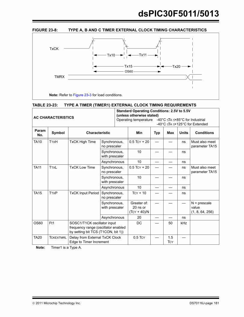
dsPIC30F5011/5013
FIGURE 23-8: TYPE A, B AND C TIMER EXTERNAL CLOCK TIMING CHARACTERISTICSTABLE 23-23: TYPE A TIMER (TIMER1) EXTERNAL CLOCK TIMING REQUIREMENTS
AC CHARACTERISTICS
Standard Operating Conditions: 2.5V to 5.5V(unless otherwise stated)Operating temperature -40°C ≤ TA ≤ +85°C for Industrial
-40°C ≤ TA ≤ +125°C for Extended
ParamNo. Symbol Characteristic Min Typ Max Units Conditions
TA10 TTXH TxCK High Time Synchronous,no prescaler
0.5 TCY + 20 — — ns Must also meet parameter TA15
Synchronous,with prescaler
10 — — ns
Asynchronous 10 — — nsTA11 TTXL TxCK Low Time Synchronous,
no prescaler0.5 TCY + 20 — — ns Must also meet
parameter TA15Synchronous,with prescaler
10 — — ns
Asynchronous 10 — — nsTA15 TTXP TxCK Input Period Synchronous,
no prescalerTCY + 10 — — ns
Synchronous,with prescaler
Greater of:20 ns or
(TCY + 40)/N
— — — N = prescale value(1, 8, 64, 256)
Asynchronous 20 — — nsOS60 Ft1 SOSC1/T1CK oscillator input
frequency range (oscillator enabled by setting bit TCS (T1CON, bit 1))
DC — 50 kHz
TA20 TCKEXTMRL Delay from External TxCK Clock Edge to Timer Increment
0.5 TCY — 1.5 TCY
—
Note: Timer1 is a Type A.
Note: Refer to Figure 23-3 for load conditions.
Tx11
Tx15
Tx10
Tx20
TMRX OS60
TxCK
© 2011 Microchip Technology Inc. DS70116J-page 181

dsPIC30F5011/5013
TABLE 23-24: TYPE B TIMER (TIMER2 AND TIMER4) EXTERNAL CLOCK TIMING REQUIREMENTS
AC CHARACTERISTICS
Standard Operating Conditions: 2.5V to 5.5V(unless otherwise stated)Operating temperature -40°C ≤ TA ≤ +85°C for Industrial
-40°C ≤ TA ≤ +125°C for Extended
ParamNo. Symbol Characteristic Min Typ Max Units Conditions
TB10 TtxH TxCK High Time Synchronous,no prescaler
0.5 TCY + 20 — — ns Must also meet parameter TB15
Synchronous,with prescaler
10 — — ns
TB11 TtxL TxCK Low Time Synchronous,no prescaler
0.5 TCY + 20 — — ns Must also meet parameter TB15
Synchronous,with prescaler
10 — — ns
TB15 TtxP TxCK Input Period Synchronous,no prescaler
TCY + 10 — — ns N = prescale value(1, 8, 64, 256)Synchronous,
with prescalerGreater of:
20 ns or(TCY + 40)/N
TB20 TCKEXT-MRL
Delay from External TxCK Clock Edge to Timer Increment
0.5 TCY — 1.5 TCY —
Note: Timer2 and Timer4 are Type B.
TABLE 23-25: TYPE C TIMER (TIMER3 AND TIMER5) EXTERNAL CLOCK TIMING REQUIREMENTS
AC CHARACTERISTICS
Standard Operating Conditions: 2.5V to 5.5V(unless otherwise stated)Operating temperature -40°C ≤ TA ≤ +85°C for Industrial
-40°C ≤ TA ≤ +125°C for Extended
ParamNo. Symbol Characteristic Min Typ Max Units Conditions
TC10 TtxH TxCK High Time Synchronous 0.5 TCY + 20 — — ns Must also meet parameter TC15
TC11 TtxL TxCK Low Time Synchronous 0.5 TCY + 20 — — ns Must also meet parameter TC15
TC15 TtxP TxCK Input Period Synchronous,no prescaler
TCY + 10 — — ns N = prescalevalue (1, 8, 64, 256)Synchronous,
with prescalerGreater of:
20 ns or (TCY + 40)/N
TC20 TCKEXT-MRL
Delay from External TxCK Clock Edge to Timer Increment
0.5 TCY — 1.5 TCY
—
Note: Timer3 and Timer5 are Type C.
DS70116J-page 182 © 2011 Microchip Technology Inc.

dsPIC30F5011/5013
FIGURE 23-9: INPUT CAPTURE (CAPx) TIMING CHARACTERISTICSTABLE 23-26: INPUT CAPTURE TIMING REQUIREMENTS
AC CHARACTERISTICS
Standard Operating Conditions: 2.5V to 5.5V(unless otherwise stated)Operating temperature -40°C ≤ TA ≤ +85°C for Industrial
-40°C ≤ TA ≤ +125°C for Extended
ParamNo. Symbol Characteristic(1) Min Max Units Conditions
IC10 TccL ICx Input Low Time No Prescaler 0.5 TCY + 20 — nsWith Prescaler 10 — ns
IC11 TccH ICx Input High Time No Prescaler 0.5 TCY + 20 — nsWith Prescaler 10 — ns
IC15 TccP ICx Input Period (2 TCY + 40)/N — ns N = prescale value (1, 4, 16)
Note 1: These parameters are characterized but not tested in manufacturing.
ICX
IC10 IC11
IC15
Note: Refer to Figure 23-3 for load conditions.
© 2011 Microchip Technology Inc. DS70116J-page 183

dsPIC30F5011/5013
FIGURE 23-10: OUTPUT COMPARE MODULE (OCx) TIMING CHARACTERISTICSTABLE 23-27: OUTPUT COMPARE MODULE TIMING REQUIREMENTS
AC CHARACTERISTICS
Standard Operating Conditions: 2.5V to 5.5V(unless otherwise stated)Operating temperature -40°C ≤ TA ≤ +85°C for Industrial
-40°C ≤ TA ≤ +125°C for Extended
Param No. Symbol Characteristic(1) Min Typ(2) Max Units Conditions
OC10 TccF OCx Output Fall Time — — — ns See Parameter DO32OC11 TccR OCx Output Rise Time — — — ns See Parameter DO31Note 1: These parameters are characterized but not tested in manufacturing.
2: Data in “Typ” column is at 5V, 25°C unless otherwise stated. Parameters are for design guidance only and are not tested.
OCx
OC11 OC10(Output Compare
Note: Refer to Figure 23-3 for load conditions.
or PWM Mode)
DS70116J-page 184 © 2011 Microchip Technology Inc.

dsPIC30F5011/5013
FIGURE 23-11: OC/PWM MODULE TIMING CHARACTERISTICSTABLE 23-28: SIMPLE OC/PWM MODE TIMING REQUIREMENTS
AC CHARACTERISTICS
Standard Operating Conditions: 2.5V to 5.5V(unless otherwise stated)Operating temperature -40°C ≤ TA ≤ +85°C for Industrial
-40°C ≤ TA ≤ +125°C for Extended
Param No. Symbol Characteristic(1) Min Typ(2) Max Units Conditions
OC15 TFD Fault Input to PWM I/O Change
— — 50 ns
OC20 TFLT Fault Input Pulse Width 50 — — nsNote 1: These parameters are characterized but not tested in manufacturing.
2: Data in “Typ” column is at 5V, 25°C unless otherwise stated. Parameters are for design guidance only and are not tested.
OCFA/OCFB
OCx
OC20
OC15
© 2011 Microchip Technology Inc. DS70116J-page 185

dsPIC30F5011/5013
FIGURE 23-12: DCI MODULE (MULTICHANNEL, I2S MODES) TIMING CHARACTERISTICSCOFS
CSCK(SCKE = 0)
CSCK(SCKE = 1)
CSDO
CSDI
CS11 CS10
CS40 CS41
CS21CS20
CS35
CS21
MSb LSb
MSb IN LSb IN
CS31
HIGH-Z HIGH-Z
70
CS30
CS51 CS50
CS55
Note: Refer to Figure 23-3 for load conditions.
CS20
CS56
DS70116J-page 186 © 2011 Microchip Technology Inc.

dsPIC30F5011/5013
TABLE 23-29: DCI MODULE (MULTICHANNEL, I2S MODES) TIMING REQUIREMENTSAC CHARACTERISTICS
Standard Operating Conditions: 2.5V to 5.5V(unless otherwise stated)Operating temperature -40°C ≤ TA ≤ +85°C for Industrial
-40°C ≤ TA ≤ +125°C for Extended
ParamNo. Symbol Characteristic(1) Min Typ(2) Max Units Conditions
CS10 TcSCKL CSCK Input Low Time(CSCK pin is an input)
TCY / 2 + 20
— — ns
CSCK Output Low Time(3)
(CSCK pin is an output)30 — — ns
CS11 TcSCKH CSCK Input High Time(CSCK pin is an input)
TCY / 2 + 20
— — ns
CSCK Output High Time(3)
(CSCK pin is an output)30 — — ns
CS20 TcSCKF CSCK Output Fall Time(4)
(CSCK pin is an output)— 10 25 ns
CS21 TcSCKR CSCK Output Rise Time(4)
(CSCK pin is an output)— 10 25 ns
CS30 TcSDOF CSDO Data Output Fall Time(4) — 10 25 nsCS31 TcSDOR CSDO Data Output Rise Time(4) — 10 25 nsCS35 TDV Clock edge to CSDO data valid — — 10 nsCS36 TDIV Clock edge to CSDO tri-stated 10 — 20 nsCS40 TCSDI Setup time of CSDI data input to
CSCK edge (CSCK pin is inputor output)
20 — — ns
CS41 THCSDI Hold time of CSDI data input toCSCK edge (CSCK pin is inputor output)
20 — — ns
CS50 TcoFSF COFS Fall Time(COFS pin is output)
— 10 25 ns Note 1
CS51 TcoFSR COFS Rise Time(COFS pin is output)
— 10 25 ns Note 1
CS55 TscoFS Setup time of COFS data input toCSCK edge (COFS pin is input)
20 — — ns
CS56 THCOFS Hold time of COFS data input toCSCK edge (COFS pin is input)
20 — — ns
Note 1: These parameters are characterized but not tested in manufacturing.2: Data in “Typ” column is at 5V, 25°C unless otherwise stated. Parameters are for design guidance only and
are not tested.3: The minimum clock period for CSCK is 100 ns. Therefore, the clock generated in Master mode must not
violate this specification.4: Assumes 50 pF load on all DCI pins.
© 2011 Microchip Technology Inc. DS70116J-page 187

dsPIC30F5011/5013
FIGURE 23-13: DCI MODULE (AC-LINK MODE) TIMING CHARACTERISTICSTABLE 23-30: DCI MODULE (AC-LINK MODE) TIMING REQUIREMENTS
AC CHARACTERISTICS
Standard Operating Conditions: 2.5V to 5.5V(unless otherwise stated)Operating temperature -40°C ≤ TA ≤ +85°C for Industrial
-40°C ≤ TA ≤ +125°C for Extended
ParamNo. Symbol Characteristic(1)(2) Min Typ(3) Max Units Conditions
CS60 TBCLKL BIT_CLK Low Time 36 40.7 45 nsCS61 TBCLKH BIT_CLK High Time 36 40.7 45 nsCS62 TBCLK BIT_CLK Period — 81.4 — ns Bit clock is inputCS65 TSACL Input Setup Time to
Falling Edge of BIT_CLK— — 10 ns
CS66 THACL Input Hold Time fromFalling Edge of BIT_CLK
— — 10 ns
CS70 TSYNCLO SYNC Data Output Low Time — 19.5 — μs Note 1CS71 TSYNCHI SYNC Data Output High Time — 1.3 — μs Note 1CS72 TSYNC SYNC Data Output Period — 20.8 — μs Note 1CS75 TRACL Rise Time, SYNC, SDATA_OUT — 10 25 ns CLOAD = 50 pF, VDD = 5VCS76 TFACL Fall Time, SYNC, SDATA_OUT — 10 25 ns CLOAD = 50 pF, VDD = 5VCS77 TRACL Rise Time, SYNC, SDATA_OUT — 10 25 ns CLOAD = 50 pF, VDD = 3VCS78 TFACL Fall Time, SYNC, SDATA_OUT — 10 25 ns CLOAD = 50 pF, VDD = 3VCS80 TOVDACL Output valid delay from rising
edge of BIT_CLK— — 15 ns
Note 1: These parameters are characterized but not tested in manufacturing.2: These values assume BIT_CLK frequency is 12.288 MHz.3: Data in “Typ” column is at 5V, 25°C unless otherwise stated. Parameters are for design guidance only and
are not tested.
SYNC
BIT_CLK
SDO
SDI
CS61 CS60
CS65 CS66
CS80
CS21
MSb IN
CS75
LSb
CS76
(COFS)
(CSCK)
LSbMSb
CS72
CS71 CS70
CS76 CS75
(CSDO)
(CSDI)
CS62 CS20
DS70116J-page 188 © 2011 Microchip Technology Inc.

dsPIC30F5011/5013
FIGURE 23-14: SPI MODULE MASTER MODE (CKE = 0) TIMING CHARACTERISTICSTABLE 23-31: SPI MASTER MODE (CKE = 0) TIMING REQUIREMENTS
AC CHARACTERISTICS
Standard Operating Conditions: 2.5V to 5.5V(unless otherwise stated)Operating temperature -40°C ≤ TA ≤ +85°C for Industrial
-40°C ≤ TA ≤ +125°C for Extended
ParamNo. Symbol Characteristic(1) Min Typ(2) Max Units Conditions
SP10 TscL SCKX Output Low Time(3) TCY / 2 — — nsSP11 TscH SCKX Output High Time(3) TCY/2 — — nsSP20 TscF SCKX Output Fall Time(4 — — — ns See parameter
DO32SP21 TscR SCKX Output Rise Time(4) — — — ns See parameter
DO31SP30 TdoF SDOX Data Output Fall Time(4) — — — ns See parameter
DO32SP31 TdoR SDOX Data Output Rise
Time(4)— — — ns See parameter
DO31SP35 TscH2doV,
TscL2doVSDOX Data Output Valid after SCKX Edge
— — 30 ns
SP40 TdiV2scH,TdiV2scL
Setup Time of SDIX Data Inputto SCKX Edge
20 — — ns
SP41 TscH2diL,TscL2diL
Hold Time of SDIX Data Inputto SCKX Edge
20 — — ns
Note 1: These parameters are characterized but not tested in manufacturing.2: Data in “Typ” column is at 5V, 25°C unless otherwise stated. Parameters are for design guidance only and
are not tested.3: The minimum clock period for SCK is 100 ns. Therefore, the clock generated in Master mode must not
violate this specification.4: Assumes 50 pF load on all SPI pins.
SCKx(CKP = 0)
SCKx(CKP = 1)
SDOx
SDIx
SP11 SP10
SP40 SP41
SP21SP20SP35
SP20SP21
MSb LSbBIT14 - - - - - -1
MSb IN LSb INBIT14 - - - -1
SP30SP31
Note: Refer to Figure 23-3 for load conditions.
© 2011 Microchip Technology Inc. DS70116J-page 189

dsPIC30F5011/5013
FIGURE 23-15: SPI MODULE MASTER MODE (CKE =1) TIMING CHARACTERISTICSTABLE 23-32: SPI MODULE MASTER MODE (CKE = 1) TIMING REQUIREMENTS
AC CHARACTERISTICS
Standard Operating Conditions: 2.5V to 5.5V(unless otherwise stated)Operating temperature -40°C ≤ TA ≤ +85°C for Industrial
-40°C ≤ TA ≤ +125°C for Extended
ParamNo. Symbol Characteristic(1) Min Typ(2) Max Units Conditions
SP10 TscL SCKX output low time(3) TCY / 2 — — nsSP11 TscH SCKX output high time(3) TCY / 2 — — nsSP20 TscF SCKX output fall time(4) — — — ns See Parameter
DO32SP21 TscR SCKX output rise time(4) — — — ns See Parameter
DO31SP30 TdoF SDOX data output fall time(4) — — — ns See Parameter
DO32SP31 TdoR SDOX data output rise time(4) — — — ns See Parameter
DO31SP35 TscH2doV
,TscL2doV
SDOX data output valid afterSCKX edge
— — 30 ns
SP36 TdoV2sc, TdoV2scL
SDOX data output setup tofirst SCKX edge
30 — — ns
SP40 TdiV2scH, TdiV2scL
Setup time of SDIX data inputto SCKX edge
20 — — ns
SP41 TscH2diL, TscL2diL
Hold time of SDIX data inputto SCKX edge
20 — — ns
Note 1: These parameters are characterized but not tested in manufacturing.2: Data in “Typ” column is at 5V, 25°C unless otherwise stated. Parameters are for design guidance only and
are not tested.3: The minimum clock period for SCK is 100 ns. Therefore, the clock generated in Master mode must not
violate this specification.4: Assumes 50 pF load on all SPI pins.
SCKX(CKP = 0)
SCKX(CKP = 1)
SDOX
SDIX
SP36
SP30,SP31
SP35
MSb
MSb IN
BIT14 - - - - - -1
LSb INBIT14 - - - -1
LSb
Note: Refer to Figure 23-3 for load conditions.
SP11 SP10 SP20SP21
SP21SP20
SP40
SP41
DS70116J-page 190 © 2011 Microchip Technology Inc.

dsPIC30F5011/5013
FIGURE 23-16: SPI MODULE SLAVE MODE (CKE = 0) TIMING CHARACTERISTICSTABLE 23-33: SPI MODULE SLAVE MODE (CKE = 0) TIMING REQUIREMENTS
AC CHARACTERISTICS
Standard Operating Conditions: 2.5V to 5.5V(unless otherwise stated)Operating temperature -40°C ≤ TA ≤ +85°C for Industrial
-40°C ≤ TA ≤ +125°C for Extended
ParamNo. Symbol Characteristic(1) Min Typ(2) Max Units Conditions
SP70 TscL SCKX Input Low Time 30 — — nsSP71 TscH SCKX Input High Time 30 — — nsSP72 TscF SCKX Input Fall Time(3) — 10 25 nsSP73 TscR SCKX Input Rise Time(3) — 10 25 nsSP30 TdoF SDOX Data Output Fall Time(3) — — — ns See Parameter DO32SP31 TdoR SDOX Data Output Rise Time(3) — — — ns See Parameter DO31SP35 TscH2doV,
TscL2doVSDOX Data Output Valid after SCKX Edge
— — 30 ns
SP40 TdiV2scH, TdiV2scL
Setup Time of SDIX Data Input to SCKX Edge
20 — — ns
SP41 TscH2diL, TscL2diL
Hold Time of SDIX Data Inputto SCKX Edge
20 — — ns
SP50 TssL2scH, TssL2scL
SSX↓ to SCKX↑ or SCKX↓ Input 120 — — ns
SP51 TssH2doZ SSX↑ to SDOX OutputHigh-Impedance(3)
10 — 50 ns
SP52 TscH2ssHTscL2ssH
SSX after SCK Edge 1.5 TCY +40
— — ns
Note 1: These parameters are characterized but not tested in manufacturing.2: Data in “Typ” column is at 5V, 25°C unless otherwise stated. Parameters are for design guidance only and
are not tested.3: Assumes 50 pF load on all SPI pins.
SSX
SCKX(CKP = 0)
SCKX(CKP = 1)
SDOX
SDI
SP50
SP40SP41
SP30,SP31 SP51
SP35
SDIX
MSb LSbBIT14 - - - - - -1
MSb IN BIT14 - - - -1 LSb IN
SP52
SP73SP72
SP72SP73SP71 SP70
Note: Refer to Figure 23-3 for load conditions.
© 2011 Microchip Technology Inc. DS70116J-page 191

dsPIC30F5011/5013
FIGURE 23-17: SPI MODULE SLAVE MODE (CKE = 1) TIMING CHARACTERISTICSSSX
SCKX(CKP = 0)
SCKX(CKP = 1)
SDOX
SDI
SP50
SP60
SDIX
SP30,SP31
MSb BIT14 - - - - - -1 LSb
SP51
MSb IN BIT14 - - - -1 LSb IN
SP35
SP52
SP52
SP73SP72
SP72SP73SP71 SP70
SP40SP41
Note: Refer to Figure 23-3 for load conditions.
DS70116J-page 192 © 2011 Microchip Technology Inc.

dsPIC30F5011/5013
TABLE 23-34: SPI MODULE SLAVE MODE (CKE = 1) TIMING REQUIREMENTSAC CHARACTERISTICS
Standard Operating Conditions: 2.5V to 5.5V(unless otherwise stated)Operating temperature -40°C ≤ TA ≤ +85°C for Industrial
-40°C ≤ TA ≤ +125°C for Extended
ParamNo. Symbol Characteristic(1) Min Typ(2) Max Units Conditions
SP70 TscL SCKX Input Low Time 30 — — nsSP71 TscH SCKX Input High Time 30 — — nsSP72 TscF SCKX Input Fall Time(3) — 10 25 nsSP73 TscR SCKX Input Rise Time(3) — 10 25 nsSP30 TdoF SDOX Data Output Fall Time(3) — — — ns See parameter
DO32SP31 TdoR SDOX Data Output Rise Time(3) — — — ns See parameter
DO31SP35 TscH2doV
,TscL2doV
SDOX Data Output Valid afterSCKX Edge
— — 30 ns
SP40 TdiV2scH, TdiV2scL
Setup Time of SDIX Data Inputto SCKX Edge
20 — — ns
SP41 TscH2diL, TscL2diL
Hold Time of SDIX Data Inputto SCKX Edge
20 — — ns
SP50 TssL2scH, TssL2scL
SSX↓ to SCKX↓ or SCKX↑ input 120 — — ns
SP51 TssH2doZ SS↑ to SDOX OutputHigh-Impedance(4)
10 — 50 ns
SP52 TscH2ssHTscL2ssH
SSX↑ after SCKX Edge 1.5 TCY + 40 — — ns
SP60 TssL2doV SDOX Data Output Valid afterSSX Edge
— — 50 ns
Note 1: These parameters are characterized but not tested in manufacturing.2: Data in “Typ” column is at 5V, 25°C unless otherwise stated. Parameters are for design guidance only and
are not tested.3: The minimum clock period for SCK is 100 ns. Therefore, the clock generated in Master mode must not
violate this specification.4: Assumes 50 pF load on all SPI pins.
© 2011 Microchip Technology Inc. DS70116J-page 193

dsPIC30F5011/5013
FIGURE 23-18: I2C™ BUS START/STOP BITS TIMING CHARACTERISTICS (MASTER MODE)FIGURE 23-19: I2C™ BUS DATA TIMING CHARACTERISTICS (MASTER MODE)
IM31 IM34SCL
SDA
StartCondition
StopCondition
IM30 IM33
Note: Refer to Figure 23-3 for load conditions.
IM11IM10 IM33
IM11IM10
IM20
IM26IM25
IM40 IM40 IM45
IM21
SCL
SDAIn
SDAOut
Note: Refer to Figure 23-3 for load conditions.
DS70116J-page 194 © 2011 Microchip Technology Inc.

dsPIC30F5011/5013
TABLE 23-35: I2C™ BUS DATA TIMING REQUIREMENTS (MASTER MODE)AC CHARACTERISTICS
Standard Operating Conditions: 2.5V to 5.5V(unless otherwise stated)Operating temperature -40°C ≤ TA ≤ +85°C for Industrial
-40°C ≤ TA ≤ +125°C for Extended
ParamNo. Symbol Characteristic Min(1) Max Units Conditions
IM10 TLO:SCL Clock Low Time 100 kHz mode TCY / 2 (BRG + 1) — µs400 kHz mode TCY / 2 (BRG + 1) — µs1 MHz mode(2) TCY / 2 (BRG + 1) — µs
IM11 THI:SCL Clock High Time 100 kHz mode TCY / 2 (BRG + 1) — µs400 kHz mode TCY / 2 (BRG + 1) — µs1 MHz mode(2) TCY / 2 (BRG + 1) — µs
IM20 TF:SCL SDA and SCLFall Time
100 kHz mode — 300 ns CB is specified to be from 10 to 400 pF400 kHz mode 20 + 0.1 CB 300 ns
1 MHz mode(2) — 100 nsIM21 TR:SCL SDA and SCL
Rise Time100 kHz mode — 1000 ns CB is specified to be
from 10 to 400 pF400 kHz mode 20 + 0.1 CB 300 ns1 MHz mode(2) — 300 ns
IM25 TSU:DAT Data InputSetup Time
100 kHz mode 250 — ns400 kHz mode 100 — ns1 MHz mode(2) — — ns
IM26 THD:DAT Data InputHold Time
100 kHz mode 0 — ns400 kHz mode 0 0.9 µs1 MHz mode(2) — — ns
IM30 TSU:STA Start ConditionSetup Time
100 kHz mode TCY / 2 (BRG + 1) — µs Only relevant for repeated Startcondition
400 kHz mode TCY / 2 (BRG + 1) — µs1 MHz mode(2) TCY / 2 (BRG + 1) — µs
IM31 THD:STA Start Condition Hold Time
100 kHz mode TCY / 2 (BRG + 1) — µs After this period thefirst clock pulse isgenerated
400 kHz mode TCY / 2 (BRG + 1) — µs1 MHz mode(2) TCY / 2 (BRG + 1) — µs
IM33 TSU:STO Stop Condition Setup Time
100 kHz mode TCY / 2 (BRG + 1) — µs400 kHz mode TCY / 2 (BRG + 1) — µs1 MHz mode(2) TCY / 2 (BRG + 1) — µs
IM34 THD:STO Stop Condition 100 kHz mode TCY / 2 (BRG + 1) — nsHold Time 400 kHz mode TCY / 2 (BRG + 1) — ns
1 MHz mode(2) TCY / 2 (BRG + 1) — nsIM40 TAA:SCL Output Valid
From Clock100 kHz mode — 3500 ns400 kHz mode — 1000 ns1 MHz mode(2) — — ns
IM45 TBF:SDA Bus Free Time 100 kHz mode 4.7 — µs Time the bus must be free before a newtransmission can start
400 kHz mode 1.3 — µs1 MHz mode(2) — — µs
IM50 CB Bus Capacitive Loading — 400 pF Note 1: BRG is the value of the I2C Baud Rate Generator. Refer to Section 21. “Inter-Integrated Circuit™ (I2C)”
in the “dsPIC30F Family Reference Manual” (DS70046).2: Maximum pin capacitance = 10 pF for all I2C pins (for 1 MHz mode only).
© 2011 Microchip Technology Inc. DS70116J-page 195

dsPIC30F5011/5013
FIGURE 23-20: I2C™ BUS START/STOP BITS TIMING CHARACTERISTICS (SLAVE MODE)FIGURE 23-21: I2C™ BUS DATA TIMING CHARACTERISTICS (SLAVE MODE)
IS31 IS34SCL
SDA
StartCondition
StopCondition
IS30 IS33
IS30IS31 IS33
IS11
IS10
IS20
IS26IS25
IS40 IS40 IS45
IS21
SCL
SDAIn
SDAOut
DS70116J-page 196 © 2011 Microchip Technology Inc.

dsPIC30F5011/5013
TABLE 23-36: I2C™ BUS DATA TIMING REQUIREMENTS (SLAVE MODE)AC CHARACTERISTICS
Standard Operating Conditions: 2.5V to 5.5V(unless otherwise stated)Operating temperature -40°C ≤ TA ≤ +85°C for Industrial
-40°C ≤ TA ≤ +125°C for Extended
ParamNo. Symbol Characteristic Min Max Units Conditions
IS10 TLO:SCL Clock Low Time 100 kHz mode 4.7 — μs Device must operate at a minimum of 1.5 MHz
400 kHz mode 1.3 — μs Device must operate at a minimum of 10 MHz.
1 MHz mode(1) 0.5 — μs —IS11 THI:SCL Clock High Time 100 kHz mode 4.0 — μs Device must operate at a
minimum of 1.5 MHz400 kHz mode 0.6 — μs Device must operate at a
minimum of 10 MHz1 MHz mode(1) 0.5 — μs
IS20 TF:SCL SDA and SCLFall Time
100 kHz mode — 300 ns CB is specified to be from10 to 400 pF400 kHz mode 20 + 0.1 CB 300 ns
1 MHz mode(1) — 100 nsIS21 TR:SCL SDA and SCL
Rise Time100 kHz mode — 1000 ns CB is specified to be from
10 to 400 pF400 kHz mode 20 + 0.1 CB 300 ns1 MHz mode(1) — 300 ns
IS25 TSU:DAT Data InputSetup Time
100 kHz mode 250 — ns400 kHz mode 100 — ns1 MHz mode(1) 100 — ns
IS26 THD:DAT Data InputHold Time
100 kHz mode 0 — ns400 kHz mode 0 0.9 μs1 MHz mode(1) 0 0.3 μs
IS30 TSU:STA Start ConditionSetup Time
100 kHz mode 4.7 — μs Only relevant for repeated Start condition400 kHz mode 0.6 — μs
1 MHz mode(1) 0.25 — μsIS31 THD:STA Start Condition
Hold Time 100 kHz mode 4.0 — μs After this period the first
clock pulse is generated400 kHz mode 0.6 — μs1 MHz mode(1) 0.25 — μs
IS33 TSU:STO Stop Condition Setup Time
100 kHz mode 4.7 — μs400 kHz mode 0.6 — μs1 MHz mode(1) 0.6 — μs
IS34 THD:STO Stop Condition 100 kHz mode 4000 — nsHold Time 400 kHz mode 600 — ns
1 MHz mode(1) 250 nsIS40 TAA:SCL Output Valid
From Clock100 kHz mode 0 3500 ns400 kHz mode 0 1000 ns1 MHz mode(1) 0 350 ns
IS45 TBF:SDA Bus Free Time 100 kHz mode 4.7 — μs Time the bus must be free before a new transmission can start
400 kHz mode 1.3 — μs1 MHz mode(1) 0.5 — μs
IS50 CB Bus Capacitive Loading — 400 pF Note 1: Maximum pin capacitance = 10 pF for all I2C™ pins (for 1 MHz mode only).
© 2011 Microchip Technology Inc. DS70116J-page 197

dsPIC30F5011/5013
FIGURE 23-22: CAN MODULE I/O TIMING CHARACTERISTICSTABLE 23-37: CAN MODULE I/O TIMING REQUIREMENTS
AC CHARACTERISTICS
Standard Operating Conditions: 2.5V to 5.5V(unless otherwise stated)Operating temperature -40°C ≤ TA ≤ +85°C for Industrial
-40°C ≤ TA ≤ +125°C for Extended
ParamNo. Symbol Characteristic(1) Min Typ(2) Max Units Conditions
CA10 TioF Port Output Fall Time — — — ns See parameter DO32
CA11 TioR Port Output Rise Time — — — ns See parameter DO31
CA20 Tcwf Pulse Width to TriggerCAN Wakeup Filter
500 — — ns
Note 1: These parameters are characterized but not tested in manufacturing.2: Data in “Typ” column is at 5V, 25°C unless otherwise stated. Parameters are for design guidance only and
are not tested.
CXTX Pin(output)
CA10 CA11
Old Value New Value
CA20
CXRX Pin(input)
DS70116J-page 198 © 2011 Microchip Technology Inc.

dsPIC30F5011/5013
TABLE 23-38: 12-BIT A/D MODULE SPECIFICATIONSAC CHARACTERISTICS
Standard Operating Conditions: 2.5V to 5.5V(unless otherwise stated)Operating temperature -40°C ≤ TA ≤ +85°C for Industrial
-40°C ≤ TA ≤ +125°C for Extended
Param No. Symbol Characteristic Min. Typ Max. Units Conditions
Device SupplyAD01 AVDD Module VDD Supply Greater of
VDD - 0.3or 2.7
— Lesser ofVDD + 0.3
or 5.5
V
AD02 AVSS Module VSS Supply VSS - 0.3 — VSS + 0.3 VReference Inputs
AD05 VREFH Reference Voltage High AVSS + 2.7 — AVDD VAD06 VREFL Reference Voltage Low AVSS — AVDD - 2.7 VAD07 VREF Absolute Reference
Voltage AVSS - 0.3 — AVDD + 0.3 V
AD08 IREF Current Drain — 150.001
2001
μAμA
A/D operatingA/D off
Analog InputAD10 VINH-VINL Full-Scale Input Span VREFL VREFH V See NoteAD11 VIN Absolute Input Voltage AVSS - 0.3 AVDD + 0.3 VAD12 — Leakage Current — ±0.001 ±0.610 μA VINL = AVSS = VREFL =
0V, AVDD = VREFH = 5VSource Impedance =2.5 kΩ
AD13 — Leakage Current — ±0.001 ±0.610 μA VINL = AVSS = VREFL = 0V, AVDD = VREFH = 3VSource Impedance =2.5 kΩ
AD17 RIN Recommended Impedance of Analog Voltage Source
— — 2.5K Ω
DC AccuracyAD20 Nr Resolution 12 data bits bitsAD21 INL Integral Nonlinearity — — <±1 LSb VINL = AVSS = VREFL =
0V, AVDD = VREFH = 5VAD21A INL Integral Nonlinearity — — <±1 LSb VINL = AVSS = VREFL =
0V, AVDD = VREFH = 3VAD22 DNL Differential Nonlinearity — — <±1 LSb VINL = AVSS = VREFL =
0V, AVDD = VREFH = 5VAD22A DNL Differential Nonlinearity — — <±1 LSb VINL = AVSS = VREFL =
0V, AVDD = VREFH = 3VAD23 GERR Gain Error +1.25 +1.5 +3 LSb VINL = AVSS = VREFL =
0V, AVDD = VREFH = 5VAD23A GERR Gain Error +1.25 +1.5 +3 LSb VINL = AVSS = VREFL =
0V, AVDD = VREFH = 3VNote 1: The A/D conversion result never decreases with an increase in the input voltage, and has no missing
codes.
© 2011 Microchip Technology Inc. DS70116J-page 199

dsPIC30F5011/5013
AD24 EOFF Offset Error -2 -1.5 -1.25 LSb VINL = AVSS = VREFL = 0V, AVDD = VREFH = 5V
AD24A EOFF Offset Error -2 -1.5 -1.25 LSb VINL = AVSS = VREFL = 0V, AVDD = VREFH = 3V
AD25 — Monotonicity(1) — — — — GuaranteedDynamic Performance
AD30 THD Total Harmonic Distortion — -71 — dBAD31 SINAD Signal to Noise and
Distortion — 68 — dB
AD32 SFDR Spurious Free DynamicRange
— 83 — dB
AD33 FNYQ Input Signal Bandwidth — — 100 kHzAD34 ENOB Effective Number of Bits 10.95 11.1 — bits
TABLE 23-38: 12-BIT A/D MODULE SPECIFICATIONS (CONTINUED)
AC CHARACTERISTICS
Standard Operating Conditions: 2.5V to 5.5V(unless otherwise stated)Operating temperature -40°C ≤ TA ≤ +85°C for Industrial
-40°C ≤ TA ≤ +125°C for Extended
Param No. Symbol Characteristic Min. Typ Max. Units Conditions
Note 1: The A/D conversion result never decreases with an increase in the input voltage, and has no missing codes.
DS70116J-page 200 © 2011 Microchip Technology Inc.
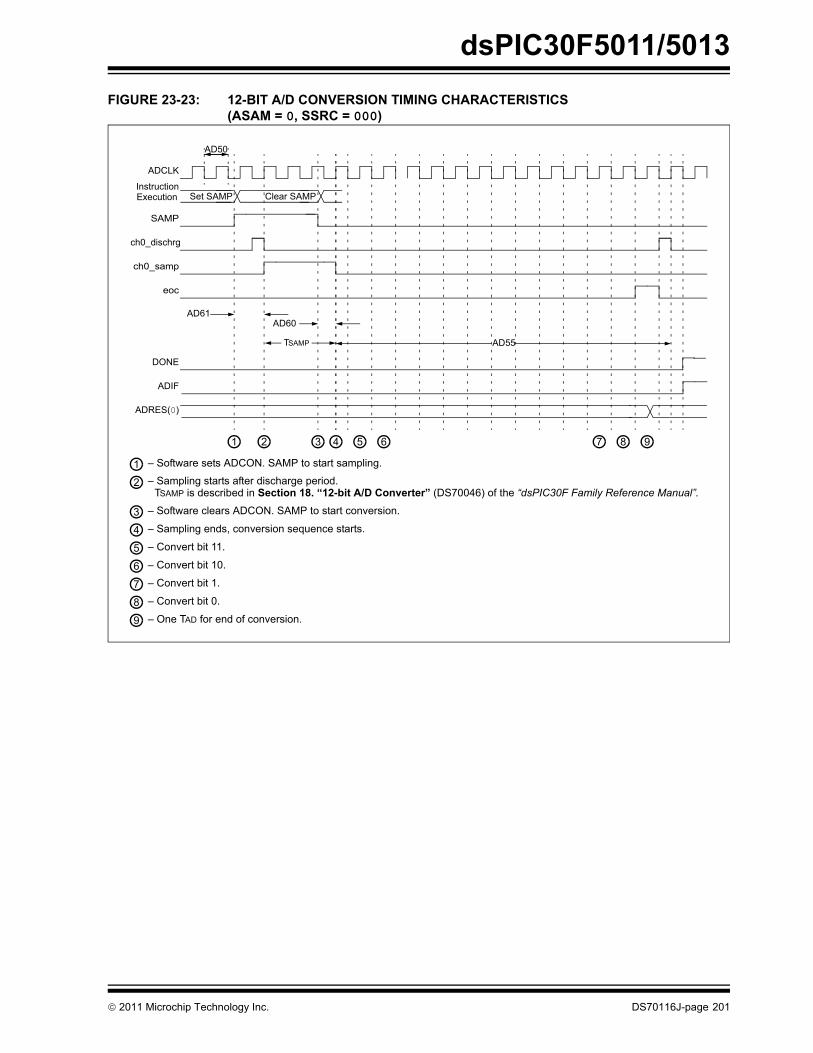
dsPIC30F5011/5013
FIGURE 23-23: 12-BIT A/D CONVERSION TIMING CHARACTERISTICS(ASAM = 0, SSRC = 000)
AD55TSAMP
Clear SAMPSet SAMP
AD61
ADCLK
Instruction
SAMP
ch0_dischrg
ch0_samp
AD60
DONE
ADIF
ADRES(0)
1 2 3 4 5 6 87
1 – Software sets ADCON. SAMP to start sampling.
2 – Sampling starts after discharge period.
3 – Software clears ADCON. SAMP to start conversion.
4 – Sampling ends, conversion sequence starts.
5 – Convert bit 11.
9 – One TAD for end of conversion.
AD50
eoc
9
6 – Convert bit 10.
7 – Convert bit 1.
8 – Convert bit 0.
Execution
TSAMP is described in Section 18. “12-bit A/D Converter” (DS70046) of the “dsPIC30F Family Reference Manual”.
© 2011 Microchip Technology Inc. DS70116J-page 201

dsPIC30F5011/5013
TABLE 23-39: 12-BIT A/D CONVERSION TIMING REQUIREMENTS
AC CHARACTERISTICS
Standard Operating Conditions: 2.7V to 5.5V(unless otherwise stated)Operating temperature -40°C ≤ TA ≤ +85°C for Industrial
-40°C ≤ TA ≤ +125°C for Extended
Param No. Symbol Characteristic Min. Typ Max. Units Conditions
Clock ParametersAD50 TAD A/D Clock Period — 334 — ns VDD = 3-5.5V (Note 1)AD51 TRC A/D Internal RC Oscillator Period 1.2 1.5 1.8 μs
Conversion RateAD55 TCONV Conversion Time — 14 TAD — nsAD56 FCNV Throughput Rate — — 200 ksps VDD = VREF = 5VAD57 TSAMP Sampling Time — 1 TAD — ns VDD = 3-5.5V source
resistanceRS = 0-2.5 kΩ
Timing ParametersAD60 TPCS Conversion Start from Sample
Trigger— 1 TAD — ns
AD61 TPSS Sample Start from SettingSample (SAMP) Bit
0.5 TAD — 1.5 TAD
ns
AD62 TCSS Conversion Completion toSample Start (ASAM = 1)
— 0.5 TAD — ns
AD63 TDPU(2) Time to Stabilize Analog Stagefrom A/D Off to A/D On
— — 20 μs
Note 1: Because the sample caps will eventually lose charge, clock rates below 10 kHz can affect linearity performance, especially at elevated temperatures.
2: TDPU is the time required for the ADC module to stabilize when it is turned on (ADCON1<ADON> = 1). During this time the ADC result is indeterminate.
DS70116J-page 202 © 2011 Microchip Technology Inc.

dsPIC30F5011/5013
24.0 PACKAGING INFORMATION
24.1 Package Marking Information
Legend: XX...X Customer-specific informationY Year code (last digit of calendar year)YY Year code (last 2 digits of calendar year)WW Week code (week of January 1 is week ‘01’)NNN Alphanumeric traceability code Pb-free JEDEC designator for Matte Tin (Sn)* This package is Pb-free. The Pb-free JEDEC designator ( )
can be found on the outer packaging for this package.
Note: In the event the full Microchip part number cannot be marked on one line, it willbe carried over to the next line, thus limiting the number of availablecharacters for customer-specific information.
3e
3e
64-Lead TQFP Example
XXXXXXXXXXXXXXXXXXXXXXXXXXXXXX
YYWWNNN
dsPIC30F5011
07160S1
80-Lead TQFP
XXXXXXXXXXXX
YYWWNNN
XXXXXXXXXXXX
Example
dsPIC
-30I/PT
-30I/PT07160S3
30F5013XXXXXXXXXXXX 3e
3e
© 2011 Microchip Technology Inc. DS70116J-page 203

dsPIC30F5011/5013
64-Lead Plastic Thin Quad Flatpack (PT) – 10x10x1 mm Body, 2.00 mm Footprint [TQFP]
Notes:1. Pin 1 visual index feature may vary, but must be located within the hatched area.2. Chamfers at corners are optional; size may vary.3. Dimensions D1 and E1 do not include mold flash or protrusions. Mold flash or protrusions shall not exceed 0.25 mm per side.4. Dimensioning and tolerancing per ASME Y14.5M.
BSC: Basic Dimension. Theoretically exact value shown without tolerances.REF: Reference Dimension, usually without tolerance, for information purposes only.
Note: For the most current package drawings, please see the Microchip Packaging Specification located at http://www.microchip.com/packaging
Units MILLIMETERSDimension Limits MIN NOM MAX
Number of Leads N 64Lead Pitch e 0.50 BSCOverall Height A – – 1.20Molded Package Thickness A2 0.95 1.00 1.05Standoff A1 0.05 – 0.15Foot Length L 0.45 0.60 0.75Footprint L1 1.00 REFFoot Angle φ 0° 3.5° 7°Overall Width E 12.00 BSCOverall Length D 12.00 BSCMolded Package Width E1 10.00 BSCMolded Package Length D1 10.00 BSCLead Thickness c 0.09 – 0.20Lead Width b 0.17 0.22 0.27Mold Draft Angle Top α 11° 12° 13°Mold Draft Angle Bottom β 11° 12° 13°
D
D1
E
E1
e
b
N
NOTE 1 1 2 3 NOTE 2
c
L
A1
L1
A2
A
φ
β
α
Microchip Technology Drawing C04-085B
DS70116J-page 204 © 2011 Microchip Technology Inc.

dsPIC30F5011/5013
80-Lead Plastic Thin Quad Flatpack (PT) – 12x12x1 mm Body, 2.00 mm Footprint [TQFP]
Notes:1. Pin 1 visual index feature may vary, but must be located within the hatched area.
2. Chamfers at corners are optional; size may vary.
3. Dimensions D1 and E1 do not include mold flash or protrusions. Mold flash or protrusions shall not exceed 0.25 mm per side.
4. Dimensioning and tolerancing per ASME Y14.5M.
BSC: Basic Dimension. Theoretically exact value shown without tolerances.
REF: Reference Dimension, usually without tolerance, for information purposes only.
Note: For the most current package drawings, please see the Microchip Packaging Specification located at
http://www.microchip.com/packaging
Units MILLIMETERS
Dimension Limits MIN NOM MAX
Number of Leads N 80
Lead Pitch e 0.50 BSC
Overall Height A – – 1.20
Molded Package Thickness A2 0.95 1.00 1.05
Standoff A1 0.05 – 0.15
Foot Length L 0.45 0.60 0.75
Footprint L1 1.00 REF
Foot Angle φ 0° 3.5° 7°
Overall Width E 14.00 BSC
Overall Length D 14.00 BSC
Molded Package Width E1 12.00 BSC
Molded Package Length D1 12.00 BSC
Lead Thickness c 0.09 – 0.20
Lead Width b 0.17 0.22 0.27
Mold Draft Angle Top α 11° 12° 13°
Mold Draft Angle Bottom β 11° 12° 13°
D
D1
E
E1
e
b N
NOTE 1123 NOTE 2
A
A2
L1A1
L
c
α
βφ
Microchip Technology Drawing C04-092B
© 2011 Microchip Technology Inc. DS70116J-page 205

dsPIC30F5011/5013
���������� ������������� ������������������ �!"#$����%���&
' �( �!���"#!��$��!����%����&�'���#(�����#��#���!�����������)��%�����������*���!������!�&��!��!!�+,,'''�"��������",���%�����
DS70116J-page 206 © 2011 Microchip Technology Inc.

dsPIC30F5011/5013
)��������� ������������� ���������#��#����� �!"#$����%���&
' �( �!���"#!��$��!����%����&�'���#(�����#��#���!�����������)��%�����������*���!������!�&��!��!!�+,,'''�"��������",���%�����
© 2011 Microchip Technology Inc. DS70116J-page 207

dsPIC30F5011/5013
NOTES:DS70116J-page 208 © 2011 Microchip Technology Inc.

dsPIC30F5011/5013
APPENDIX A: REVISION HISTORY
Revision F (May 2006)Previous versions of this data sheet containedAdvance or Preliminary Information. They were distrib-uted with incomplete characterization data.
Revision F of this document reflects the followingupdates:
• Supported I2C Slave Addresses (see Table 15-1)
• ADC Conversion Clock selection to allow 200 kHz sampling rate (see Section 19.0 “12-bit Analog-to-Digital Converter (ADC) Module”
• Operating Current (Idd) Specifications (see Table 23-5)
• BOR voltage limits (see Table 23-11)
• I/O pin Input Specifications (see Table 23-8)
• Watchdog Timer time-out limits (see Table 23-21)
Revision G (January 2007)This revision includes updates to the packaging diagrams.
Revision H (March 2008)This revision includes the following updates:
• Added FUSE Configuration Register (FICD) details (see Section 20.7 “Device Configuration Registers” and Table 20-8)
• Updated FGS Configuration register details (see Table 20-8)
• Removed erroneous statement regarding genera-tion of CAN receive errors (see Section 17.4.5 “Receive Errors”)
• Electrical Specifications:- Resolved TBD values for parameters DO10,
DO16, DO20, and DO26 (see Table 23-9)- 10-bit High-Speed ADC tPDU timing parame-
ter (time to stabilize) has been updated from 20 µs typical to 20 µs maximum (see Table 23-39)
- Parameter OS65 (Internal RC Accuracy) has been expanded to reflect multiple Min and Max values for different temperatures (see Table 23-19)
- Parameter DC12 (RAM Data Retention Volt-age) has been updated to include a Min value (see Table 23-4)
- Parameter D134 (Erase/Write Cycle Time) has been updated to include Min and Max values and the Typ value has been removed (see Table 23-12)
- Removed parameters OS62 (Internal FRC Jitter) and OS64 (Internal FRC Drift) and Note 2 from AC Characteristics (see Table 23-18)
- Parameter OS63 (Internal FRC Accuracy) has been expanded to reflect multiple Min and Max values for different temperatures (see Table 23-18)
- Updated Min and Max values and Conditions for parameter SY11 and updated Min, Typ, and Max values and Conditions for parame-ter SY20 (see Table 23-21)
• Additional minor corrections throughout the document
© 2011 Microchip Technology Inc. DS70116J-page 209

dsPIC30F5011/5013
Revision J (January 2011)This revision includes minor typographical andformatting changes throughout the data sheet text.The major changes are referenced by their respectivesection in Table A-1.
TABLE A-1: MAJOR SECTION UPDATESSection Name Update Description
Section 20.0 “System Integration”
Added a shaded note on OSCTUN functionality in Section 20.2.5 “Fast RC Oscillator (FRC)”.
Section 23.0 “Electrical Characteristics”
Updated the maximum value for parameter DI19 and the minimum value for parameter DI29 in the I/O Pin Input Specifications (see Table 23-8).
Removed parameter D136 and updated the minimum, typical, maximum, and conditions for parameters D122 and D134 in the Program and EEPROM specifications (see Table 23-12).
DS70116J-page 210 © 2011 Microchip Technology Inc.

dsPIC30F5011/5013
INDEXNumerics12-bit Analog-to-Digital Converter (A/D) Module .............. 127AA/D .................................................................................... 127
Aborting a Conversion .............................................. 129ADCHS Register ....................................................... 127ADCON1 Register..................................................... 127ADCON2 Register..................................................... 127ADCON3 Register..................................................... 127ADCSSL Register ..................................................... 127ADPCFG Register..................................................... 127Configuring Analog Port Pins.............................. 58, 134Connection Considerations....................................... 134Conversion Operation ............................................... 128Effects of a Reset...................................................... 133Operation During CPU Idle Mode ............................. 133Operation During CPU Sleep Mode.......................... 133Output Formats ......................................................... 133Power-down Modes .................................................. 133Programming the Sample Trigger............................. 129Register Map............................................................. 135Result Buffer ............................................................. 128Sampling Requirements............................................ 132Selecting the Conversion Sequence......................... 128
AC Characteristics ............................................................ 173Internal LPRC Accuracy............................................ 176Load Conditions ........................................................ 173
AC Temperature and Voltage Specifications .................... 173AC-Link Mode Operation .................................................. 124
16-bit Mode ............................................................... 12420-bit Mode ............................................................... 125
ADCSelecting the Conversion Clock ................................ 129
ADC Conversion Speeds .................................................. 130Address Generator Units .................................................... 41Alternate Vector Table ........................................................ 39Analog-to-Digital Converter. See A/D.Assembler
MPASM Assembler................................................... 160Automatic Clock Stretch...................................................... 94
During 10-bit Addressing (STREN = 1)....................... 94During 7-bit Addressing (STREN = 1)......................... 94Receive Mode ............................................................. 94Transmit Mode ............................................................ 94
BBandgap Start-up Time
Requirements............................................................ 180Timing Characteristics .............................................. 180
Barrel Shifter ....................................................................... 22Bit-Reversed Addressing .................................................... 44
Example ...................................................................... 44Implementation ........................................................... 44Modifier Values Table ................................................. 45Sequence Table (16-Entry)......................................... 45
Block Diagrams12-bit A/D Functional ................................................ 12716-bit Timer1 Module .................................................. 6316-bit Timer2............................................................... 6916-bit Timer3............................................................... 6916-bit Timer4............................................................... 7416-bit Timer5............................................................... 74
32-bit Timer2/3 ........................................................... 6832-bit Timer4/5 ........................................................... 73CAN Buffers and Protocol Engine ............................ 108DCI Module............................................................... 118Dedicated Port Structure ............................................ 57DSP Engine ................................................................ 19dsPIC30F5011............................................................ 10dsPIC30F5013............................................................ 11External Power-on Reset Circuit .............................. 145I2C .............................................................................. 92Input Capture Mode.................................................... 77Oscillator System...................................................... 139Output Compare Mode ............................................... 81Reset System ........................................................... 143Shared Port Structure................................................. 58SPI.............................................................................. 88SPI Master/Slave Connection..................................... 88UART Receiver......................................................... 100UART Transmitter....................................................... 99
BOR Characteristics ......................................................... 172BOR. See Brown-out Reset.Brown-out Reset
Characteristics.......................................................... 171Timing Requirements ............................................... 179
CC Compilers
MPLAB C18.............................................................. 160CAN Module ..................................................................... 107
Baud Rate Setting .................................................... 112CAN1 Register Map.................................................. 114Frame Types ............................................................ 107I/O Timing Characteristics ........................................ 198I/O Timing Requirements.......................................... 198Message Reception.................................................. 110Message Transmission............................................. 111Modes of Operation .................................................. 109Overview................................................................... 107
CLKOUT and I/O TimingCharacteristics.......................................................... 177Requirements ........................................................... 177
Code ExamplesData EEPROM Block Erase ....................................... 54Data EEPROM Block Write ........................................ 56Data EEPROM Read.................................................. 53Data EEPROM Word Erase ....................................... 54Data EEPROM Word Write ........................................ 55Erasing a Row of Program Memory ........................... 49Initiating a Programming Sequence ........................... 50Loading Write Latches................................................ 50
Code Protection................................................................ 137Control Registers ................................................................ 48
NVMADR .................................................................... 48NVMADRU ................................................................. 48NVMCON.................................................................... 48NVMKEY .................................................................... 48
Core ArchitectureOverview..................................................................... 15
CPU Architecture Overview................................................ 15Customer Change Notification Service............................. 215Customer Notification Service .......................................... 215Customer Support............................................................. 215
DData Accumulators and Adder/Subtractor .......................... 20
Data Space Write Saturation ...................................... 22
© 2011 Microchip Technology Inc. DS70116J-page 211

dsPIC30F5011/5013
Overflow and Saturation ............................................. 20Round Logic ................................................................ 21Write Back................................................................... 21Data Address Space ........................................................... 28Alignment .................................................................... 30Alignment (Figure) ...................................................... 30Effect of Invalid Memory Accesses (Table)................. 30MCU and DSP (MAC Class) Instructions Example..... 29Memory Map ............................................................... 28Near Data Space ........................................................ 31Software Stack............................................................ 31Spaces ........................................................................ 30Width........................................................................... 30
Data Converter Interface (DCI) Module ............................ 117Data EEPROM Memory ...................................................... 53
Erasing........................................................................ 54Erasing, Block ............................................................. 54Erasing, Word ............................................................. 54Protection Against Spurious Write .............................. 56Reading....................................................................... 53Write Verify ................................................................. 56Writing......................................................................... 55Writing, Block .............................................................. 56Writing, Word .............................................................. 55
DC Characteristics ............................................................ 164BOR .......................................................................... 172Brown-out Reset ....................................................... 171I/O Pin Output Specifications .................................... 170Idle Current (IIDLE) .................................................... 167Low-Voltage Detect................................................... 170LVDL ......................................................................... 171Operating Current (IDD)............................................. 165Power-Down Current (IPD) ........................................ 168Program and EEPROM............................................. 172Temperature and Voltage Specifications .................. 165
DCI ModuleBit Clock Generator................................................... 121Buffer Alignment with Data Frames .......................... 123Buffer Control ............................................................ 117Buffer Data Alignment............................................... 117Buffer Length Control ................................................ 123COFS Pin.................................................................. 117CSCK Pin.................................................................. 117CSDI Pin ................................................................... 117CSDO Mode Bit ........................................................ 124CSDO Pin ................................................................. 117Data Justification Control Bit ..................................... 122Device Frequencies for Common Codec CSCK Frequen-
cies (Table) ....................................................... 121Digital Loopback Mode ............................................. 124Enable....................................................................... 119Frame Sync Generator ............................................. 119Frame Sync Mode Control Bits ................................. 119I/O Pins ..................................................................... 117Interrupts................................................................... 124Introduction ............................................................... 117Master Frame Sync Operation.................................. 119Operation .................................................................. 119Operation During CPU Idle Mode ............................. 124Operation During CPU Sleep Mode.......................... 124Receive Slot Enable Bits........................................... 122Receive Status Bits................................................... 123Register Map............................................................. 126Sample Clock Edge Control Bit................................. 122Slave Frame Sync Operation.................................... 119
Slot Enable Bits Operation with Frame Sync............ 122Slot Status Bits ......................................................... 124Synchronous Data Transfers .................................... 122Timing Characteristics
AC-Link Mode................................................... 188Multichannel, I2S Modes................................... 186
Timing RequirementsAC-Link Mode................................................... 188Multichannel, I2S Modes................................... 187
Transmit Slot Enable Bits ......................................... 122Transmit Status Bits.................................................. 123Transmit/Receive Shift Register ............................... 117Underflow Mode Control Bit...................................... 124Word Size Selection Bits .......................................... 119
Development Support ....................................................... 159Device Configuration
Register Map ............................................................ 150Device Configuration Registers
FBORPOR................................................................ 148FBS........................................................................... 148FGS .......................................................................... 148FOSC........................................................................ 148FSS........................................................................... 148FWDT ....................................................................... 148
Device Overview................................................................... 9Disabling the UART .......................................................... 101Divide Support .................................................................... 18
Instructions (Table) ..................................................... 18DSP Engine ........................................................................ 18
Multiplier ..................................................................... 20Dual Output Compare Match Mode .................................... 82
Continuous Pulse Mode.............................................. 82Single Pulse Mode...................................................... 82
EElectrical Characteristics .................................................. 163
AC............................................................................. 173DC ............................................................................ 164
Enabling and Setting Up UARTSetting Up Data, Parity and Stop Bit Selections ....... 101
Enabling the UART ........................................................... 101Equations
ADC Conversion Clock ............................................. 129Baud Rate................................................................. 103Bit Clock Frequency.................................................. 121COFSG Period.......................................................... 119Serial Clock Rate........................................................ 96Time Quantum for Clock Generation ........................ 113
Errata .................................................................................... 7Exception Sequence
Trap Sources .............................................................. 37External Clock Timing Characteristics
Type A, B and C Timer ............................................. 181External Clock Timing Requirements ............................... 174
Type A Timer ............................................................ 181Type B Timer ............................................................ 182Type C Timer ............................................................ 182
External Interrupt Requests ................................................ 39
FFast Context Saving ........................................................... 39Flash Program Memory ...................................................... 47
II/O Ports.............................................................................. 57
Parallel (PIO) .............................................................. 57
DS70116J-page 212 © 2011 Microchip Technology Inc.

dsPIC30F5011/5013
I2C 10-bit Slave Mode Operation ........................................ 93Reception.................................................................... 94Transmission............................................................... 94
I2C 7-bit Slave Mode Operation .......................................... 93Reception.................................................................... 93Transmission............................................................... 93
I2C Master Mode Operation ................................................ 95Baud Rate Generator.................................................. 96Clock Arbitration.......................................................... 96Multi-Master Communication, Bus Collision and Bus Ar-
bitration ............................................................... 96Reception.................................................................... 95Transmission............................................................... 95
I2C Master Mode Support ................................................... 95I2C Module .......................................................................... 91
Addresses ................................................................... 93Bus Data Timing Characteristics
Master Mode..................................................... 194Slave Mode....................................................... 196
Bus Data Timing RequirementsMaster Mode..................................................... 195Slave Mode....................................................... 197
Bus Start/Stop Bits Timing CharacteristicsMaster Mode..................................................... 194Slave Mode....................................................... 196
General Call Address Support .................................... 95Interrupts..................................................................... 95IPMI Support ............................................................... 95Operating Function Description .................................. 91Operation During CPU Sleep and Idle Modes ............ 96Pin Configuration ........................................................ 91Programmer’s Model................................................... 91Register Map............................................................... 97Registers..................................................................... 91Slope Control .............................................................. 95Software Controlled Clock Stretching (STREN = 1).... 94Various Modes ............................................................ 91
I2S Mode Operation .......................................................... 125Data Justification....................................................... 125Frame and Data Word Length Selection................... 125
Idle Current (IIDLE) ............................................................ 167In-Circuit Serial Programming (ICSP) ......................... 47, 137Input Capture (CAPX) Timing Characteristics .................. 183Input Capture Module ......................................................... 77
Interrupts..................................................................... 78Register Map............................................................... 79
Input Capture Operation During Sleep and Idle Modes ...... 78CPU Idle Mode............................................................ 78CPU Sleep Mode ........................................................ 78
Input Capture Timing Requirements ................................. 183Input Change Notification Module....................................... 62
dsPIC30F5011 Register Map (Bits 15-8) .................... 62dsPIC30F5011 Register Map (Bits 7-0) ...................... 62dsPIC30F5013 Register Map (Bits 15-8) .................... 62dsPIC30F5013 Register Map (Bits 7-0) ...................... 62
Instruction Addressing Modes............................................. 41File Register Instructions ............................................ 41Fundamental Modes Supported.................................. 41MAC Instructions......................................................... 42MCU Instructions ........................................................ 41Move and Accumulator Instructions............................ 42Other Instructions........................................................ 42
Instruction SetOverview ................................................................... 154Summary................................................................... 151
Internal Clock Timing Examples ....................................... 175Internet Address ............................................................... 215Interrupt Controller
Register Map .............................................................. 40Interrupt Priority .................................................................. 36
Traps .......................................................................... 37Interrupt Sequence ............................................................. 39
Interrupt Stack Frame................................................. 39Interrupts ............................................................................ 35
LLoad Conditions................................................................ 173Low Voltage Detect (LVD) ................................................ 147Low-Voltage Detect Characteristics.................................. 170LVDL Characteristics ........................................................ 171
MMemory Organization ......................................................... 23
Core Register Map ..................................................... 32Microchip Internet Web Site.............................................. 215Modes of Operation
Disable...................................................................... 109Initialization............................................................... 109Listen All Messages.................................................. 109Listen Only................................................................ 109Loopback .................................................................. 109Normal Operation ..................................................... 109
Modulo Addressing............................................................. 42Applicability................................................................. 44Incrementing Buffer Operation Example .................... 43Start and End Address ............................................... 43W Address Register Selection.................................... 43
MPLAB ASM30 Assembler, Linker, Librarian................... 160MPLAB Integrated Development Environment Software.. 159MPLAB PM3 Device Programmer .................................... 162MPLAB REAL ICE In-Circuit Emulator System ................ 161MPLINK Object Linker/MPLIB Object Librarian ................ 160
NNVM
Register Map .............................................................. 51
OOC/PWM Module Timing Characteristics ......................... 185Operating Current (IDD) .................................................... 165Oscillator
Configurations .......................................................... 140Fail-Safe Clock Monitor .................................... 142Fast RC (FRC).................................................. 141Initial Clock Source Selection........................... 140Low Power RC (LPRC)..................................... 141LP Oscillator Control......................................... 140Phase Locked Loop (PLL) ................................ 141Start-up Timer (OST)........................................ 140
Operating Modes (Table).......................................... 138System Overview...................................................... 137
Oscillator Selection........................................................... 137Oscillator Start-up Timer
Timing Characteristics .............................................. 178Timing Requirements ............................................... 179
Output Compare Interrupts ................................................. 84Output Compare Module .................................................... 81
Register Map .............................................................. 85Timing Characteristics .............................................. 184Timing Requirements ............................................... 184
Output Compare Operation During CPU Idle Mode ........... 84
© 2011 Microchip Technology Inc. DS70116J-page 213

dsPIC30F5011/5013
Output Compare Sleep Mode Operation............................. 84PPackaging Information ...................................................... 203
Marking ..................................................................... 203Peripheral Module Disable (PMD) Registers .................... 149Pinout Descriptions ............................................................. 12PLL Clock Timing Specifications....................................... 175POR. See Power-on Reset.Port Write/Read Example.................................................... 58PORTA
Register Map for dsPIC30F5013 ................................ 59PORTB
Register Map for dsPIC30F5011/5013 ....................... 59PORTC
Register Map for dsPIC30F5011 ................................ 59Register Map for dsPIC30F5013 ................................ 59
PORTDRegister Map for dsPIC30F5011 ................................ 60Register Map for dsPIC30F5013 ................................ 60
PORTFRegister Map for dsPIC30F5011 ................................ 60Register Map for dsPIC30F5013 ................................ 61
PORTGRegister Map for dsPIC30F5011/5013 ....................... 61
Power Saving Modes ........................................................ 147Idle ............................................................................ 148Sleep......................................................................... 147Sleep and Idle ........................................................... 137
Power-Down Current (IPD) ................................................ 168Power-up Timer
Timing Characteristics .............................................. 178Timing Requirements................................................ 179
Program Address Space ..................................................... 23Construction................................................................ 24Data Access from Program Memory Using Program
Space Visibility.................................................... 26Data Access From Program Memory Using Table In-
structions............................................................. 25Data Access from, Address Generation...................... 24Data Space Window into Operation............................ 27Data Table Access (LS Word) .................................... 25Data Table Access (MS Byte) ..................................... 26Memory Map ............................................................... 23Table Instructions
TBLRDH.............................................................. 25TBLRDL .............................................................. 25TBLWTH ............................................................. 25TBLWTL.............................................................. 25
Program and EEPROM Characteristics ............................ 172Program Counter................................................................. 16Programmable................................................................... 137Programmer’s Model........................................................... 16
Diagram ...................................................................... 17Programming Operations .................................................... 49
Algorithm for Program Flash ....................................... 49Erasing a Row of Program Memory............................ 49Initiating the Programming Sequence......................... 50Loading Write Latches ................................................ 50
Protection Against Accidental Writes to OSCCON ........... 142
RReader Response ............................................................. 216Reset......................................................................... 137, 143
BOR, Programmable................................................. 145Brown-out Reset (BOR) ............................................ 137
Oscillator Start-up Timer (OST) ................................ 137POR
Operating without FSCM and PWRT................ 145With Long Crystal Start-up Time ...................... 145
POR (Power-on Reset)............................................. 143Power-on Reset (POR)............................................. 137Power-up Timer (PWRT) .......................................... 137
Reset Sequence ................................................................. 37Reset Sources ............................................................ 37
Reset SourcesBrown-out Reset (BOR).............................................. 37Illegal Instruction Trap ................................................ 37Trap Lockout............................................................... 37Uninitialized W Register Trap ..................................... 37Watchdog Time-out .................................................... 37
Reset Timing Characteristics............................................ 178Reset Timing Requirements ............................................. 179Run-Time Self-Programming (RTSP) ................................. 47
SSimple Capture Event Mode............................................... 77
Buffer Operation ......................................................... 78Hall Sensor Mode ....................................................... 78Prescaler .................................................................... 77Timer2 and Timer3 Selection Mode............................ 78
Simple OC/PWM Mode Timing Requirements ................. 185Simple Output Compare Match Mode ................................ 82Simple PWM Mode ............................................................. 82
Input Pin Fault Protection ........................................... 82Period ......................................................................... 83
Software Simulator (MPLAB SIM) .................................... 161Software Stack Pointer, Frame Pointer .............................. 16
CALL Stack Frame ..................................................... 31SPI Module ......................................................................... 87
Framed SPI Support ................................................... 87Operating Function Description .................................. 87Operation During CPU Idle Mode............................... 89Operation During CPU Sleep Mode............................ 89SDOx Disable ............................................................. 87Slave Select Synchronization ..................................... 89SPI1 Register Map...................................................... 90SPI2 Register Map...................................................... 90Timing Characteristics
Master Mode (CKE = 0).................................... 189Master Mode (CKE = 1).................................... 190Slave Mode (CKE = 1).............................. 191, 192
Timing RequirementsMaster Mode (CKE = 0).................................... 189Master Mode (CKE = 1).................................... 190Slave Mode (CKE = 0)...................................... 191Slave Mode (CKE = 1)...................................... 193
Word and Byte Communication.................................. 87Status Bits, Their Significance and the Initialization Condition
for RCON Register, Case 1 ...................................... 146Status Bits, Their Significance and the Initialization Condition
for RCON Register, Case 2 ...................................... 146Status Register ................................................................... 16Symbols Used in Opcode Descriptions ............................ 152System Integration............................................................ 137
Register Map ............................................................ 150
TTable Instruction Operation Summary ................................ 47Temperature and Voltage Specifications
AC............................................................................. 173Timer1 Module.................................................................... 63
DS70116J-page 214 © 2011 Microchip Technology Inc.
dsPIC30F5011/5013
16-bit Asynchronous Counter Mode ........................... 6316-bit Synchronous Counter Mode ............................. 6316-bit Timer Mode....................................................... 63Gate Operation ........................................................... 64Interrupt....................................................................... 64Operation During Sleep Mode .................................... 64Prescaler..................................................................... 64Real-Time Clock ......................................................... 64Interrupts............................................................. 64Oscillator Operation ............................................ 64
Register Map............................................................... 65Timer2 and Timer3 Selection Mode.................................... 82Timer2/3 Module ................................................................. 67
16-bit Timer Mode....................................................... 6732-bit Synchronous Counter Mode ............................. 6732-bit Timer Mode....................................................... 67ADC Event Trigger...................................................... 70Gate Operation ........................................................... 70Interrupt....................................................................... 70Operation During Sleep Mode .................................... 70Register Map............................................................... 71Timer Prescaler........................................................... 70
Timer4/5 Module ................................................................. 73Register Map............................................................... 75
Timing CharacteristicsA/D Conversion
Low-speed (ASAM = 0, SSRC = 000) .............. 201Bandgap Start-up Time............................................. 180CAN Module I/O........................................................ 198CLKOUT and I/O....................................................... 177DCI Module
AC-Link Mode ................................................... 188Multichannel, I2S Modes................................... 186
External Clock........................................................... 173I2C Bus Data
Master Mode..................................................... 194Slave Mode....................................................... 196
I2C Bus Start/Stop BitsMaster Mode..................................................... 194Slave Mode....................................................... 196
Input Capture (CAPX) ............................................... 183OC/PWM Module ...................................................... 185Oscillator Start-up Timer ........................................... 178Output Compare Module........................................... 184Power-up Timer ........................................................ 178Reset......................................................................... 178SPI Module
Master Mode (CKE = 0) .................................... 189Master Mode (CKE = 1) .................................... 190Slave Mode (CKE = 0) ...................................... 191Slave Mode (CKE = 1) ...................................... 192
Type A, B and C Timer External Clock ..................... 181Watchdog Timer........................................................ 178
Timing DiagramsCAN Bit ..................................................................... 112Frame Sync, AC-Link Start of Frame........................ 120Frame Sync, Multi-Channel Mode ............................ 120I2S Interface Frame Sync.......................................... 120PWM Output ............................................................... 83Time-out Sequence on Power-up (MCLR Not Tied to
VDD), Case 1..................................................... 144Time-out Sequence on Power-up (MCLR Not Tied to
VDD), Case 2..................................................... 144Time-out Sequence on Power-up (MCLR Tied to VDD) ..
144
Timing Diagrams and SpecificationsDC Characteristics - Internal RC Accuracy .............. 175
Timing Diagrams.See Timing CharacteristicsTiming Requirements
A/D ConversionLow-speed........................................................ 202
Bandgap Start-up Time ............................................ 180Brown-out Reset....................................................... 179CAN Module I/O ....................................................... 198CLKOUT and I/O ...................................................... 177DCI Module
AC-Link Mode................................................... 188Multichannel, I2S Modes................................... 187
External Clock .......................................................... 174I2C Bus Data (Master Mode) .................................... 195I2C Bus Data (Slave Mode) ...................................... 197Input Capture............................................................ 183Oscillator Start-up Timer........................................... 179Output Compare Module .......................................... 184Power-up Timer ........................................................ 179Reset ........................................................................ 179Simple OC/PWM Mode ............................................ 185SPI Module
Master Mode (CKE = 0).................................... 189Master Mode (CKE = 1).................................... 190Slave Mode (CKE = 0)...................................... 191Slave Mode (CKE = 1)...................................... 193
Type A Timer External Clock.................................... 181Type B Timer External Clock.................................... 182Type C Timer External Clock.................................... 182Watchdog Timer ....................................................... 179
Timing SpecificationsPLL Clock ................................................................. 175PLL Jitter .................................................................. 175
Trap Vectors ....................................................................... 38
UUART Module
Address Detect Mode ............................................... 103Auto Baud Support ................................................... 104Baud Rate Generator ............................................... 103Enabling and Setting Up........................................... 101Framing Error (FERR) .............................................. 103Idle Status................................................................. 103Loopback Mode ........................................................ 103Operation During CPU Sleep and Idle Modes.......... 104Overview..................................................................... 99Parity Error (PERR) .................................................. 103Receive Break .......................................................... 103Receive Buffer (UxRXB)........................................... 102Receive Buffer Overrun Error (OERR Bit) ................ 102Receive Interrupt ...................................................... 102Receiving Data ......................................................... 102Receiving in 8-bit or 9-bit Data Mode ....................... 102Reception Error Handling ......................................... 102Transmit Break ......................................................... 102Transmit Buffer (UxTXB) .......................................... 101Transmit Interrupt ..................................................... 102Transmitting Data ..................................................... 101Transmitting in 8-bit Data Mode ............................... 101Transmitting in 9-bit Data Mode ............................... 101UART1 Register Map ............................................... 105UART2 Register Map ............................................... 105
UART OperationIdle Mode.................................................................. 104Sleep Mode .............................................................. 104
© 2011 Microchip Technology Inc. DS70116J-page 215

dsPIC30F5011/5013
Unit ID Locations............................................................... 137Universal Asynchronous Receiver Transmitter (UART) Mod-ule ............................................................................... 99
WWake-up from Sleep ......................................................... 137Wake-up from Sleep and Idle.............................................. 39Watchdog Timer
Timing Characteristics .............................................. 178Timing Requirements................................................ 179
Watchdog Timer (WDT) ............................................ 137, 147Enabling and Disabling ............................................. 147Operation .................................................................. 147
WWW Address.................................................................. 215WWW, On-Line Support........................................................ 7
DS70116J-page 216 © 2011 Microchip Technology Inc.

dsPIC30F5011/5013
THE MICROCHIP WEB SITEMicrochip provides online support via our WWW site atwww.microchip.com. This web site is used as a meansto make files and information easily available tocustomers. Accessible by using your favorite Internetbrowser, the web site contains the followinginformation:
• Product Support – Data sheets and errata, application notes and sample programs, design resources, user’s guides and hardware support documents, latest software releases and archived software
• General Technical Support – Frequently Asked Questions (FAQ), technical support requests, online discussion groups, Microchip consultant program member listing
• Business of Microchip – Product selector and ordering guides, latest Microchip press releases, listing of seminars and events, listings of Microchip sales offices, distributors and factory representatives
CUSTOMER CHANGE NOTIFICATION SERVICEMicrochip’s customer notification service helps keepcustomers current on Microchip products. Subscriberswill receive e-mail notification whenever there arechanges, updates, revisions or errata related to aspecified product family or development tool of interest.
To register, access the Microchip web site atwww.microchip.com. Under “Support”, click on“Customer Change Notification” and follow theregistration instructions.
CUSTOMER SUPPORTUsers of Microchip products can receive assistancethrough several channels:
• Distributor or Representative• Local Sales Office• Field Application Engineer (FAE)• Technical Support• Development Systems Information Line
Customers should contact their distributor,representative or field application engineer (FAE) forsupport. Local sales offices are also available to helpcustomers. A listing of sales offices and locations isincluded in the back of this document.
Technical support is available through the web siteat: http://support.microchip.com
© 2011 Microchip Technology Inc. DS70116J-page 217

dsPIC30F5011/5013
READER RESPONSEIt is our intention to provide you with the best documentation possible to ensure successful use of your Microchipproduct. If you wish to provide your comments on organization, clarity, subject matter, and ways in which ourdocumentation can better serve you, please FAX your comments to the Technical Publications Manager at(480) 792-4150.
Please list the following information, and use this outline to provide us with your comments about this document.
TO: Technical Publications ManagerRE: Reader Response
Total Pages Sent ________
From: Name
CompanyAddressCity / State / ZIP / Country
Telephone: (_______) _________ - _________
Application (optional):
Would you like a reply? Y N
Device: Literature Number:
Questions:
FAX: (______) _________ - _________
DS70116JdsPIC30F5011/5013
1. What are the best features of this document?
2. How does this document meet your hardware and software development needs?
3. Do you find the organization of this document easy to follow? If not, why?
4. What additions to the document do you think would enhance the structure and subject?
5. What deletions from the document could be made without affecting the overall usefulness?
6. Is there any incorrect or misleading information (what and where)?
7. How would you improve this document?
DS70116J-page 218 © 2011 Microchip Technology Inc.

© 2011 Microchip Technology Inc. DS70116J-page 219
dsPIC30F5011/5013
PRODUCT IDENTIFICATION SYSTEMTo order or obtain information, e.g., on pricing or delivery, refer to the factory or the listed sales office.
d s P I C 3 0 F 5 0 1 3 AT- 3 0 I / P T- E S
Example:dsPIC30F5013AT-30I/PT = 30 MIPS, Industrial temp., TQFP package, Rev. A
Trademark
Architecture
Flash
E = Extended High Temp -40°C to +125°CI = Industrial -40°C to +85°CTemperature
Device ID
PackagePT = TQFP 10x10PT = TQFP 12x12S = Die (Waffle Pack)W = Die (Wafers)Memory Size in Bytes
0 = ROMless1 = 1K to 6K2 = 7K to 12K3 = 13K to 24K4 = 25K to 48K5 = 49K to 96K6 = 97K to 192K7 = 193K to 384K8 = 385K to 768K9 = 769K and Up
Custom ID (3 digits) or
T = Tape and Reel
A,B,C… = Revision Level
Engineering Sample (ES)
Speed20 = 20 MIPS30 = 30 MIPS

DS70116J-page 220 © 2011 Microchip Technology Inc.
AMERICASCorporate Office2355 West Chandler Blvd.Chandler, AZ 85224-6199Tel: 480-792-7200 Fax: 480-792-7277Technical Support: http://support.microchip.comWeb Address: www.microchip.comAtlantaDuluth, GA Tel: 678-957-9614 Fax: 678-957-1455BostonWestborough, MA Tel: 774-760-0087 Fax: 774-760-0088ChicagoItasca, IL Tel: 630-285-0071 Fax: 630-285-0075ClevelandIndependence, OH Tel: 216-447-0464 Fax: 216-447-0643DallasAddison, TX Tel: 972-818-7423 Fax: 972-818-2924DetroitFarmington Hills, MI Tel: 248-538-2250Fax: 248-538-2260KokomoKokomo, IN Tel: 765-864-8360Fax: 765-864-8387Los AngelesMission Viejo, CA Tel: 949-462-9523 Fax: 949-462-9608Santa ClaraSanta Clara, CA Tel: 408-961-6444Fax: 408-961-6445TorontoMississauga, Ontario, CanadaTel: 905-673-0699 Fax: 905-673-6509
ASIA/PACIFICAsia Pacific OfficeSuites 3707-14, 37th FloorTower 6, The GatewayHarbour City, KowloonHong KongTel: 852-2401-1200Fax: 852-2401-3431Australia - SydneyTel: 61-2-9868-6733Fax: 61-2-9868-6755China - BeijingTel: 86-10-8528-2100 Fax: 86-10-8528-2104China - ChengduTel: 86-28-8665-5511Fax: 86-28-8665-7889China - ChongqingTel: 86-23-8980-9588Fax: 86-23-8980-9500China - Hong Kong SARTel: 852-2401-1200 Fax: 852-2401-3431China - NanjingTel: 86-25-8473-2460Fax: 86-25-8473-2470China - QingdaoTel: 86-532-8502-7355Fax: 86-532-8502-7205China - ShanghaiTel: 86-21-5407-5533 Fax: 86-21-5407-5066China - ShenyangTel: 86-24-2334-2829Fax: 86-24-2334-2393China - ShenzhenTel: 86-755-8203-2660 Fax: 86-755-8203-1760China - WuhanTel: 86-27-5980-5300Fax: 86-27-5980-5118China - XianTel: 86-29-8833-7252Fax: 86-29-8833-7256China - XiamenTel: 86-592-2388138 Fax: 86-592-2388130China - ZhuhaiTel: 86-756-3210040 Fax: 86-756-3210049
ASIA/PACIFICIndia - BangaloreTel: 91-80-3090-4444 Fax: 91-80-3090-4123India - New DelhiTel: 91-11-4160-8631Fax: 91-11-4160-8632India - PuneTel: 91-20-2566-1512Fax: 91-20-2566-1513Japan - YokohamaTel: 81-45-471- 6166 Fax: 81-45-471-6122Korea - DaeguTel: 82-53-744-4301Fax: 82-53-744-4302Korea - SeoulTel: 82-2-554-7200Fax: 82-2-558-5932 or 82-2-558-5934Malaysia - Kuala LumpurTel: 60-3-6201-9857Fax: 60-3-6201-9859Malaysia - PenangTel: 60-4-227-8870Fax: 60-4-227-4068Philippines - ManilaTel: 63-2-634-9065Fax: 63-2-634-9069SingaporeTel: 65-6334-8870Fax: 65-6334-8850Taiwan - Hsin ChuTel: 886-3-6578-300Fax: 886-3-6578-370Taiwan - KaohsiungTel: 886-7-213-7830Fax: 886-7-330-9305Taiwan - TaipeiTel: 886-2-2500-6610 Fax: 886-2-2508-0102Thailand - BangkokTel: 66-2-694-1351Fax: 66-2-694-1350
EUROPEAustria - WelsTel: 43-7242-2244-39Fax: 43-7242-2244-393Denmark - CopenhagenTel: 45-4450-2828 Fax: 45-4485-2829France - ParisTel: 33-1-69-53-63-20 Fax: 33-1-69-30-90-79Germany - MunichTel: 49-89-627-144-0 Fax: 49-89-627-144-44Italy - Milan Tel: 39-0331-742611 Fax: 39-0331-466781Netherlands - DrunenTel: 31-416-690399 Fax: 31-416-690340Spain - MadridTel: 34-91-708-08-90Fax: 34-91-708-08-91UK - WokinghamTel: 44-118-921-5869Fax: 44-118-921-5820
Worldwide Sales and Service
08/04/10