dual functional transparent film for proximity and pressure sensing · dual functional transparent...
TRANSCRIPT

Dual functional transparent film for proximity andpressure sensing
Bo Zhang1,§, Zemin Xiang1,§, Siwei Zhu1, Qiyi Hu1, Yuanzhi Cao1, Junwen Zhong1, Qize Zhong1, Bo Wang1,2,
Yunsheng Fang1, Bin Hu1 (), Jun Zhou1, and Zhonglin Wang3
1 Wuhan National Laboratory for Optoelectronics (WNLO), School of Optical and Electronic Information, Huazhong University of
Science and Technology (HUST), Wuhan 430074, China 2 Department of Electrical Engineering and Automation, Luoyang Institute of Science and Technology, Luoyang 471023, China 3 School of Materials Science and Engineering, Georgia Institute of Technology, Atlanta, Georgia 30332-0245, USA § These authors contributed equally to this work.
Received: 14 April 2014
Revised: 3 June 2014
Accepted: 7 June 2014
© Tsinghua University Press
and Springer-Verlag Berlin
Heidelberg 2014
KEYWORDS
proximity sensor,
pressure sensor,
mutual capacitance,
silver nanowire,
transparent film
ABSTRACT
Over the past few years, the rapid development of tactile sensing technology
has contributed significantly to the realization of intuitional touch control and
intelligent human–machine interaction. Apart from physical touch or pressure
sensing, proximity sensing as a complementary function can extend the detection
mode of common single functional tactile sensors. In this work, we present a
transparent, matrix-structure dual functional capacitive sensor which integrates
the capability of proximity and pressure sensing in one device, and the excellent
spatial resolution offered by the isolated response of capacitive pixels enables
us to realize precise location identification of approaching objects and loaded
pressure with fast response, high stability and high reversibility.
1 Introduction
Planar touch sensors, as the pivotal component of
accessible man–machine interaction systems, are capable
of recognizing tactile information through monitoring
either capacitance or resistive change, and they have
promoted the revolutionary development of portable
electronics [1]. Recent advances, from device design
to manufacturing techniques, have endowed the touch
sensor with various novel characteristics, including
high flexibility [2, 3], high pressure sensitivity [4], high
spatial-resolution [5], and even self-healing capability
[6] to mimic the properties of natural skin by electronic
or optical means [7, 8]. For these devices, physical
Nano Research 2014, 7(10): 1488–1496
DOI 10.1007/s12274-014-0510-3
Address correspondence to Bin Hu, [email protected]

www.theNanoResearch.com∣www.Springer.com/journal/12274 | Nano Research
1489 Nano Res. 2014, 7(10): 1488–1496
contact between sensors and objects is essential for
triggering the response regardless the applied weight
and shape of the objects, e.g., as contact-mode-based
sensors that are “blind” to the approaching objects.
To address this issue, proximity sensing as a comple-
mentary function can be incorporated into such artificial
skin to provide a dual functional sensing capability
[9–11], which could expand the applications of common
single functional pressure sensors—for instance helping
robots to detect objects for collision avoidance and
take pre-action in the dark, or enabling a smart phone
to sense the hovering fingers with accurate positions
and distance from the screen. Among different detection
mechanisms, such as infrared light, ultrasonic waves
and magnetic induction [12, 13], proximity sensors
based on capacitance measurement are attractive
considering their easy fabrication and integration
[14], and can detect an approaching object whilst
being insensitive to the colour and texture. On the
other hand, capacitance change monitoring can also
be used for pressure sensing and has been widely
studied [15–18]. Therefore, finding an economical
and efficient way to merge isolated capacitance-based
pressure sensors and proximity sensors in one device
with seamless response and switching can add more
functions to the sensors.
Here in this work, based on the widely used
orthogonally patterned electrodes structure, we studied
the continuous response of pressure and proximity
sensing using a highly transparent film. The device is
capable of quantitatively detecting and distinguishing
objects in three different states—namely proximity,
contact and pressure-loading—by monitoring the
capacitance change between two transparent electrodes
made of a silver nanowire (AgNWs) network [19–21].
Moreover, we demonstrated that the device has good
multiple point spatial resolution in proximity mode,
something which has rarely previously been reported.
2 Result and discussion
As shown in the schematic illustration in Fig. 1(a), the
capacitive sensor was designed as a sandwich structure,
as employed in many previous studies [22–25]. A
polyethylene terephthalate (PET) sheet was used as
the substrate with parallel electrode stripes patterned
on it. Two such PET substrates were bonded together
using elastic polydimethylsiloxane (PDMS) as the
dielectric layer with top and bottom electrode stripes
placed orthogonally (row-and-column electrodes). In
the pursuit of high transparency to satisfy the requi-
rements of touch screen applications [26], an AgNWs
network was selected as the electrode [27, 28], and
was assembled by crossing AgNWs (Fig. 1(b)) with
diameters and lengths around 200 nm and hundreds
of micrometers (Figs. S1(a) and S1(b), in the Electronic
Supplementary Material (ESM)). The mechanical
robustness and conductivity could be improved by
self-welding of AgNWs junctions after plasma irradi-
ation (Fig. S1(c)). Compared with stretchable bulk-like
AgNWs electrodes [25, 29], the thin AgNWs network
exhibited percolative behaviour which renders the
transmittance of electrodes as high as 95% (Fig. S1(d))
with the sheet resistance as low as 54 ohm/sq [19, 30].
The stripe electrodes were obtained by wiping off the
AgNWs that were uncovered by the mask, which
is an efficient and simple method for large scale
fabrication (Fig. S2, in the ESM). Figure 1(c) shows the
transmittance of three different parts of as-fabricated
devices—which were acquired from the monolayer
AgNWs network covered area, the overlapping area
and the interspace area—with transmittance of 81%,
77%, and 85%, respectively, at the wavelength of
550 nm. A photograph of the bent film is shown in
the inset. From the enhanced contrast picture in
Fig. S1(d) (inset), the AgNWs electrode stripes with
line width and separation space ~4 mm can be clearly
seen, and these parameters can be customized to
meet a specified resolution.
The response mechanism of the device is based on
a capacitive sensing scheme. However, two types of
capacitance, self-capacitance (Cs) and mutual cap-
acitance (Cm) [31, 32], coexist in the device, and Fig. 1(d)
shows the schematic image and corresponding
equivalent circuit of the capacitive sensor in measu-
rements. Specifically, Cs, the capacitance of the AgNWs
electrode stripe with respect to ground, is significantly
increased by forming parasitic capacitance (Cp) between
the electrode and an approaching object, such as
human fingers [33]. Although the proximity sensor in
the Cs implementation enables us to detect the location
of an approaching object by identifying the row

| www.editorialmanager.com/nare/default.asp
1490 Nano Res. 2014, 7(10): 1488–1496
and column electrodes with the largest changes in
capacitance, its high susceptibility to environmental
interference—such as humidity, air velocity, and even
human body movement (Fig. S3, in the ESM)—
hampered qualitative analysis in practical applications.
Furthermore, a bigger issue is the appearance of
ghost points for multi-point object detection, which
result from the virtual intersections in locations other
than where the objects are really located [31, 32]. These
problems limit the applications of Cs-based proximity
sensing. In comparison, Cm can be considered as the
capacitance between two charge-holding objects, i.e.
the overlapping intersections of AgNWs electrode
stripes, which is relatively stable due to the sealed
capacitive structure with accessible measurement.
Thus the ghost points can be eliminated, allowing
accurate multiple-point location identification, as we
demonstrate in the following.
As shown in Fig. 2(a), when a grounded conductive
object (a finger was used here to simulate the real
environment) came close to an intersection (as illus-
trated in the inset), the change of Cm (ΔC, denoting
the absolute capacitance change) depended on the
change of height d (the distance from the intersection
to the finger tip), and the rate of Cm change is defined
as ΔC/C0, where C0 denotes the original Cm. The baseline
of Cm for the device-under-test without proximity or
pressure was 3.054 pF, and this value varied for different
devices. In principle, with the proximity of a finger,
the shortened d should result in the increase of Cp
between the finger and electrode, because the electric
field between the two electrodes at the intersection
will be disturbed by the finger and some of the electric
field will be shunted, thus reducing the measured Cm
as illustrated in Fig. 2(b) [34]. That is to say, Cm
increased with increasing d while Cs had the opposite
trend. As seen in Fig. 2(a), the Cm changed more
obviously for small d, implying higher sensitivity in
this range. We compared the experimental results
and values simulated using effective theory [35] to fit
Figure 1 Characterization of the structure and equivalent circuit of the sensor. (a) Schematic illustration of the sandwich structure sensor, with the AgNWs network stripes used as the row and column electrodes arranged orthogonally on the top and bottom PET substrates. (b) The corresponding SEM image of the AgNWs network. (c) Transmittance curves of different areas of the device. (d) Equivalent circuit of the capacitive sensor in measurements (Csr and Csc denote the Cs of row and column electrodes, respectively, and Rsr and Rsc denote the equivalent resistance of row and column electrodes, respectively).

www.theNanoResearch.com∣www.Springer.com/journal/12274 | Nano Research
1491 Nano Res. 2014, 7(10): 1488–1496
the change in ΔC/C0 (Fig. S4, in the ESM), and found
that for close proximity detection (d < 4 cm), the
theoretical values and measured values are more
consistent, which is probable due to the prominent
influence of Cp on the Cm, while for distant proximity
detection, the deviation becomes larger since the
interference of the surrounding environment on the
objects cannot be neglected. The corresponding response
of five adjacent intersections to a single hovering
finger is shown in Fig. 2(c) using a contour map,
which clearly demonstrates the variation of Cm with d.
The central dashed box is the intersection position
(pixel) where the finger is hovering right above, and
the other dashed boxes correspond to adjacent pixels.
When d decreases from 3 to 0.5 cm, the most significant
change in ΔC/C0 can be observed in the center. We
note that the ΔC/C0 of the left and right pixels are
larger than the values for the top and bottom ones
(bottom panel in Fig. 2(c)), which is because the
finger has an oval shape rather than the standard
circle, indicating the excellent geometric discrimination
capability of the device.
In order to study the response performance of the
sensor, Fig. 2(d) shows the capacitance variations
when a finger approached and moved away for four
cycles; the device showed good reversibility and
stability with fast response, which offers the possibility
to achieve precise proximity detection. It is worth
mentioning that, by virtue of the unique measurement
mechanism, proximity sensing based on Cm can avoid
the advent of the ghost points and allow theoretically
unlimited object detection with unambiguous location
identification [36]. To demonstrate the good spatial
resolution and multi-point proximity sensing, two
hovering metal bars (cross-section diameter ~1 cm2)
were placed right above the adjacent pixels of a
64-pixel sensor (marked by the black dashed box
with h ~1 cm) as seen in Fig. 2(e). Notable changes of
Figure 2 Characterization of the capacitive proximity response of matrix-structured sensor. (a) Change in capacitance (ΔC/C0) versusheight d (vertical distance from the overlapping intersection of AgNWs electrodes to the finger tip). (b) Schematic images of a hoveringfinger's influence on Cm. (c) Contour images of the estimated capacitance change profile of a central pixel and its four nearest neighborswhen a finger approached with different d (3, 1 and 0.5 cm). (d) Plot of ΔC/C0 versus response time with approaching and moving awayfor four cycles. (e) Proximity sensing to two metal bars with d ~1 cm, with the intersections marked by black dashed boxes.

| www.editorialmanager.com/nare/default.asp
1492 Nano Res. 2014, 7(10): 1488–1496
ΔC/C0 in these two areas can be clearly observed from
the contour image, and the excellent independent
response of each pixel without crosstalk is a benefit
of the Cm based sensing mode, which indicates its
potential applications in non-touch multi-point gesture
operation for a screen. In principle, the space distance
between the adjacent pixels decides the spatial
resolution of the sensor (the width of the AgNWs
electrode stripes and their interval distance). Moreover,
improvements in manufacturing technique can narrow
the size of the electrode and interval space, which can
enhance the spatial resolution, although the base Cm
of each pixel would decrease.
Apart from precise proximity detection, the Cm
based sensor can handle detection in the contact mode
and can serve as a pressure sensor as well [22, 24, 37],
which cannot be realized in a Cs based sensor. In brief,
each intersection in the matrix-structure represents a
unit of a simplified parallel-plate capacitor and its
capacitance is proportional to 1/D, where D is the
thickness of the PDMS dielectric layer. When the
device was subjected to pressure, the PDMS layer
was compressed, thus D decreased, and Fig. 3(a) shows
the ΔC/C0 changed with increasing pressure. In the
low-pressure range (up to 50 kPa), ΔC/C0 was linearly
dependent on pressure (Fig. 3(a) inset), while at higher
pressures the slope gradually became flat and the
pressure tended to be saturated, owing to the increasing
elastic resistance of PDMS. Comparing with a pre-
viously reported result [4], the pressure sensitivity S
(defined as the slope of the curve, S = δ(ΔC/C0)/δP) of
our device is not very high (~0.4 MPa–1); this is due to
the relatively compact structure of the flat PDMS
layer (Poisson ratio 0.5, Young’s modulus 750 kPa).
The sensitivity could be improved by fabricating
microstructure on the PDMS films [4], but this would
Figure 3 Characterization of the capacitive pressure response of matrix-structured sensor. (a) Plot of ΔC/C0 versus applied pressure up to 260 kPa (the inset shows the linear relationship up to 50 kPa). (b) The reversible response of ΔC/C0 to the applied step-up and step-down pressures (0, 25, 50, and 100 kPa). (c) Contour images of the estimated capacitance change profile of a central pixel and its four nearest neighbors when the central pixel was loaded with different pressures (50, 100 and 200 kPa).
www.theNanoResearch.com∣www.Springer.com/journal/12274 | Nano Research
1493 Nano Res. 2014, 7(10): 1488–1496
decrease the high transmittance of the film because of
the resulting light scattering, and its desirability
would depend on the specific application. In addition,
the sensor could retain high stability and reversibility
even when subjected to high pressure up to 100 kPa,
and the fast capacitance switching with applied
step-up and step-down pressures showed symmetric
jumps without hysteresis (Fig. 3(b)), while the durability
test demonstrated its steady response to a 100 kPa,
2 Hz pressure for 200 cycles (Fig. S5, in the ESM). This
large dynamic range of detectable pressure and stable
performance make the device capable of withstanding
harsh industrial field environments. We also studied
the spatial resolution in the pressure sensing, as
shown in Fig. 3(c) [38, 39]. When applying a pressure
(1 cm2 square of glass sheet), the ΔC/C0 of the central
pixel where the load applied is around six times
higher than the average for adjacent pixels, and thus
the pressure location can be determined easily. The
tiny increase of ΔC/C0 for the adjacent four pixels is
probably due to the pressure causing a geometric
shape deformation.
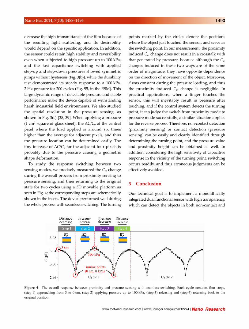
To study the response switching between two
sensing modes, we precisely measured the Cm change
during the overall process from proximity sensing to
pressure sensing, and then returning to the original
state for two cycles using a 3D movable platform as
seen in Fig. 4; the corresponding steps are schematically
shown in the insets. The device performed well during
the whole process with seamless switching. The turning
points marked by the circles denote the positions
where the object just touched the sensor, and serve as
the switching point. In our measurement, the proximity
induced Cm change does not result in a crosstalk with
that generated by pressure, because although the Cm
changes induced in these two ways are of the same
order of magnitude, they have opposite dependence
on the direction of movement of the object. Moreover,
d was constant during the pressure loading, and thus
the proximity induced Cm change is negligible. In
practical applications, when a finger touches the
sensor, this will inevitably result in pressure after
touching, and if the control system detects the turning
point, it can judge the switch from proximity mode to
pressure mode successfully; a similar situation applies
for the reverse process. Therefore, non-contact detection
(proximity sensing) or contact detection (pressure
sensing) can be easily and clearly identified through
determining the turning point, and the pressure value
and proximity height can be obtained as well. In
addition, considering the high sensitivity of capacitive
response in the vicinity of the turning point, switching
occurs readily, and thus erroneous judgments can be
effectively avoided.
3 Conclusion
Our technical goal is to implement a monolithically
integrated dual functional sensor with high transparency,
which can detect the objects in both non-contact and
Figure 4 The overall response between proximity and pressure sensing with seamless switching. Each cycle contains four steps,(step 1) approaching from 3 to 0 cm, (step 2) applying pressure up to 100 kPa, (step 3) releasing and (step 4) returning back to theoriginal position.

| www.editorialmanager.com/nare/default.asp
1494 Nano Res. 2014, 7(10): 1488–1496
mechanical contact modes. The Cm-based sensor we
have demonstrated here is a qualified candidate for
this purpose. It can sense proximity and pressure in
one device and make a seamless switch and precise
response to the overall physical process with a fast
response, high stability and high reversibility. Mean-
while, the good isolation of each pixel in the matrix-
structure leads to accurate spatial sensing and location
identification. With refinement [40], this powerful
integrated proximity–contact sensor can be applied
in smart phones, game machines and robots, but is
not limited to these.
4 Experimental
4.1 Synthesis of AgNWs ink
The AgNWs was synthesized followed previous
work [19]. Polyvinyl pyrrolidone (PVP) (0.26 g, Mw =
~1,300,000) and FeCl3 (0.15 mg) were added sequentially
to a vessel and mixed with ethylene glycol (50 mL),
and then the mixture was stirred moderately for
10 min. The solution was then heated at 180 °C for
half an hour in an oven, and then cooled down to
room temperature in a glass dryer. AgNO3 powder
(0.1168 g) was then added to the solution with
vigorous stirring for 10 min until it was fully dissolved.
Then the solution was sealed in a bottle and kept at
145 °C for 7 h in the oven. Finally, the obtained products
were washed with acetone and alcohol several times,
and stored in alcohol before use. The morphology,
structure, and composition of the samples were probed
by a scanning electron microscope (SEM, FEI Nova
NanoSEM 450).
4.2 Electrical and optical measurements
We measured Cm with a LCR meter (HIOKI IM3533-1)
with 200 kHz AC signal source, and the variation of
Cm with pressure was measured by applying a com-
pressive force perpendicular to the film which was
placed between a force gauge and a movable platform
with a glass slide placed on it (contact area ~1 cm2).
The curve of Cm versus d was plotted through adjusting
d of the conductive objects, which were fastened onto
the movable platform with a ruler with millimetre
precision (including finger and metal bar, only
conductive objects were considered in the sensor
analyses). The optical transmission of the AgNWs
network film was measured using a UV2550 spectro-
photometer, and all the values of transmission were
in the visible light spectrum (400–800 nm), and the
transmission of AgNWs network deposited PET sheet
was taken at 550 nm.
4.3 Generation of the capacitance change contour
map
The contour maps of single-point proximity sensing
and pressure sensing were generated according to the
data of the central pixel where proximity or pressure
was applied, and the data from the adjacent four pixels.
The map of double-point proximity was created based
on two central pixels with all the adjacent pixels and
intermediate pixels. A simple bilinear interpolation
was applied to estimate capacitance change in order
to create a data table and convert into a contour map.
Acknowledgements
This work was supported by the National Natural
Science Foundation of China (No. 61204001), and
the Fundamental Research Funds for the Central
Universities of China (No. 2014QN013). We also thank
the Center for Nanoscale Characterization & Devices
(CNCD), WNLO of HUST for the use of facilities in
support of this work.
Electronic Supplementary Material: Supplementary
material (details of AgNWs deposition and performance,
fabrication of the matrix-structure capacitive sensor,
the response of Cm and Cs to the environmental
interference, the use of effective theory to deal with
the parasitic capacitance analysis, and cycle durability
tests) is available in the online version of this article
at http://dx.doi.org/10.1007/s12274-014-0510-3.
References
[1] Maheshwari, V.; Saraf, R. F. High-resolution thin-film
device to sense texture by touch. Science 2006, 312, 1501–
1504.

www.theNanoResearch.com∣www.Springer.com/journal/12274 | Nano Research
1495 Nano Res. 2014, 7(10): 1488–1496
[2] Hu, B.; Chen, W.; Zhou, J. High performance flexible sensor
based on inorganic nanomaterials. Sensor. Actuat. B 2013,
176, 522–533.
[3] Hu, B.; Ding, Y.; Chen, W.; Kulkarni, D.; Shen, Y.; Tsukruk,
V. V.; Wang, Z. L. External-strain induced insulating phase
transition in VO2 nanobeam and its application as flexible
strain sensor. Adv. Mater. 2010, 22, 5134–5139.
[4] Mannsfeld, S. C.; Tee, B. C. K.; Stoltenberg, R. M.; Chen,
C. V. H. H.; Barman, S.; Muir, B. V. O.; Sokolov, A. N.;
Reese, C.; Bao, Z. N. Highly sensitive flexible pressure
sensors with microstructured rubber dielectric layers. Nat.
Mater. 2010, 9, 859–864.
[5] Wu, W. Z.; Wen, X. N.; Wang, Z. L. Taxel-addressable
matrix of vertical-nanowire piezotronic transistors for active
and adaptive tactile imaging. Science 2013, 340, 952–957.
[6] Tee, B. C. K.; Wang, C.; Allen, R.; Bao, Z. N. An electrically
and mechanically self-healing composite with pressure- and
flexion-sensitive properties for electronic skin applications.
Nat. Nanotechnol. 2012, 7, 825–832.
[7] Wang, C.; Hwang, D.; Yu, Z. B.; Takei, K.; Park, J.; Chen,
T.; Ma, B. W.; Javey, A. User-interactive electronic skin for
instantaneous pressure visualization. Nat. Mater. 2013, 12,
899–904.
[8] Ramuz, M.; Tee, B. C. K.; Tok, J. B. H.; Bao, Z. N.
Transparent, optical, pressure-sensitive artificial skin for
large-area stretchable electronics. Adv. Mater. 2012, 24,
3223–3227.
[9] Lee, H. K.; Chang, S. I.; Yoon, E. Dual-mode capacitive
proximity sensor for robot application: Implementation of
tactile and proximity sensing capability on a single polymer
platform using shared electrodes. IEEE Sens. J. 2009, 9,
1748–1755.
[10] Sadler, D. J.; Ahn, C. H. On-chip eddy current sensor for
proximity sensing and crack detection. Sensor. Actuat. A
2001, 91, 340–345.
[11] Gueissaz, F.; Piguet, D. The microreed, an ultra-small passive
MEMS magnetic proximity sensor designed for portable
applications. In The 14th IEEE International Conference on
Micro Electro Mechanical Systems, Interlaken, Switzerland,
2001, pp 269–273.
[12] Canali, C.; De Cicco, G.; Morten, B.; Prudenziati, M.; Taroni,
A. A temperature compensated ultrasonic sensor operating
in air for distance and proximity measurements. IEEE Trans.
Ind. Electron. 1982, IE-29, 336–341.
[13] Balek, D.; Kelley, R. Using gripper mounted infrared
proximity sensors for robot feedback control. In 1985 IEEE
International Conference on Robotics and Automation, St.
Louis, USA, 1985, pp 282–287.
[14] Chen, Z. H.; Luo, R. C. Design and implementation of
capacitive proximity sensor using microelectromechanical
systems technology. IEEE Trans. Ind. Electron. 1998, 45,
886–894.
[15] Takamatsu, S.; Yamashita, T.; Imai, T.; Itoh, T. Fabric touch
sensors using projected self-capacitive touch technique.
Sens. Mater. 2013, 25, 627–634.
[16] Kim, H. K.; Lee, S.; Yun, K. S. Capacitive tactile sensor
array for touch screen application. Sensor. Actuat. A 2011,
165, 2–7.
[17] Guo, S. W.; Guo, J.; Ko, W. H. A monolithically integrated
surface micromachined touch mode capacitive pressure
sensor. Sensor. Actuat. A 2000, 80, 224–232.
[18] Ko, W. H.; Wang, Q. Touch mode capacitive pressure sensors.
Sensor. Actuat. A 1999, 75, 242–251.
[19] Zhu, S. W.; Gao, Y.; Hu, B.; Li, J.; Su, J.; Fan, Z. Y.; Zhou, J.
Transferable self-welding silver nanowire network as high
performance transparent flexible electrode. Nanotechnology
2013, 24, 335202.
[20] Lee, J.; Lee, P.; Lee, H.; Lee, D.; Lee, S. S.; Ko, S. H. Very
long Ag nanowire synthesis and its application in a highly
transparent, conductive and flexible metal electrode touch
panel. Nanoscale 2012, 4, 6408–6414.
[21] De, S.; Higgins, T. M.; Lyons, P. E.; Doherty, E. M.;
Nirmalraj, P. N.; Blau, W. J.; Boland, J. J.; Coleman, J. N.
Silver nanowire networks as flexible, transparent, conducting
films: Extremely high DC to optical conductivity ratios. ACS
Nano 2009, 3, 1767–1774.
[22] Lipomi, D. J.; Vosgueritchian, M.; Tee, B. C. K.; Hellstrom,
S. L.; Lee, J. A.; Fox, C. H.; Bao, Z. N. Skin-like pressure
and strain sensors based on transparent elastic films of carbon
nanotubes. Nat. Nanotechnol. 2011, 6, 788–792.
[23] Vandeparre, H.; Watson, D.; Lacour, S. P. Extremely robust
and conformable capacitive pressure sensors based on
flexible polyurethane foams and stretchable metallization.
Appl. Phys. Lett. 2013, 103, 204103.
[24] Hu, W. L.; Niu, X. F.; Zhao, R.; Pei, Q. B. Elastomeric
transparent capacitive sensors based on an interpenetrating
composite of silver nanowires and polyurethane. Appl. Phys.
Lett. 2013, 102, 083303.
[25] Yao, S. S.; Zhu, Y. Wearable multifunctional sensors using
printed stretchable conductors made of silver nanowires.
Nanoscale 2014, 6, 2345–2352.
[26] Hecht, D. S.; Hu, L. B.; Irvin, G. Emerging transparent
electrodes based on thin films of carbon nanotubes, graphene,
and metallic nanostructures. Adv. Mater. 2011, 23, 1482–
1513.
[27] Hu, L. B.; Kim, H. S.; Lee, J. Y.; Peumans, P.; Cui, Y.
Scalable coating and properties of transparent, flexible,
silver nanowire electrodes. ACS Nano 2010, 4, 2955–2963.

| www.editorialmanager.com/nare/default.asp
1496 Nano Res. 2014, 7(10): 1488–1496
[28] Kim, T. Y.; Kim, Y. W.; Lee, H. S.; Kim, H.; Yang, W. S.;
Suh, K. S. Uniformly interconnected silver-nanowire networks
for transparent film heaters. Adv. Funct. Mater. 2013, 23,
1250–1255.
[29] Xu, F.; Zhu, Y. Highly conductive and stretchable silver
nanowire conductors. Adv. Mater. 2012, 24, 5117–5122.
[30] Bergin, S. M.; Chen, Y. H.; Rathmell, A. R.; Charbonneau,
P.; Li, Z. Y.; Wiley, B. J. The effect of nanowire length and
diameter on the properties of transparent, conducting nanowire
films. Nanoscale 2012, 4, 1996–2004.
[31] Barrett, G.; Omote, R. Projected-capacitive touch technology.
Information Display 2010, 3, 16–21.
[32] Wang, T.; Blankenship, T. Projected capacitive touch systems
from the controller point of view. Information Display 2011,
3, 8–11.
[33] Tartagni, M.; Guerrieri, R. A fingerprint sensor based on
the feedback capacitive sensing scheme. IEEE J. Solid-State
Circuits 1998, 33, 133–142.
[34] Cotton, D. P. J.; Graz, I. M.; Lacour, S. P. A multifunctional
capacitive sensor for stretchable electronic skins. IEEE Sens.
J. 2009, 9, 2008–2009.
[35] Li, N.; Zhu, H. Y.; Wang, W. Y.; Gong, Y. Parallel double-
plate capacitive proximity sensor modelling based on effective
theory. AIP Adv. 2014, 4, 027119.
[36] Ko, S.; Shin, H.; Lee, J.; Jang, H.; So, B. C.; Yun, I.; Lee, K.
Low noise capacitive sensor for multi-touch mobile handset’s
applications. In 2010 IEEE Asian Solid-State Circuits
Conference (A-SSCC), Beijing, China, 2010, pp 1–4.
[37] Yamada, T.; Hayamizu, Y.; Yamamoto, Y.; Yomogida, Y.;
Izadi-Najafabadi, A.; Futaba, D. N.; Hata, K. A stretchable
carbon nanotube strain sensor for human-motion detection.
Nat. Nanotechnol. 2011, 6, 296–301.
[38] Someya, T.; Sekitani, T.; Iba, S.; Kato, Y.; Kawaguchi, H.;
Sakurai, T. A large-area, flexible pressure sensor matrix
with organic field-effect transistors for artificial skin
applications. Proc. Natl. Acad. Sci. USA 2004, 101, 9966–
9970.
[39] Kane, B. J.; Cutkosky, M. R.; Kovacs, G. T. A traction stress
sensor array for use in high-resolution robotic tactile imaging.
J. Microelectromech. Syst. 2000, 9, 425–434.
[40] He, M. X.; Liu, R.; Li, Y.; Wang, H.; Lu, X.; Ding, G. F.; Wu,
J. J.; Zhang, T.; Zhao, X. L. Tactile probing system based
on micro-fabricated capacitive sensor. Sensor. Actuat. A 2013,
194, 128–134.