dual-output low-dropout voltage regulators with power · pdf file2.5v v in1 v in2 en seq v...
TRANSCRIPT
1FEATURES
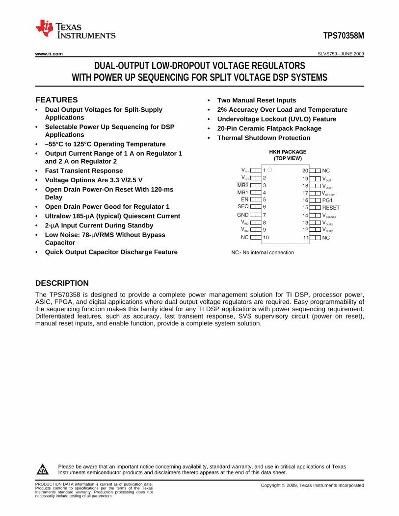
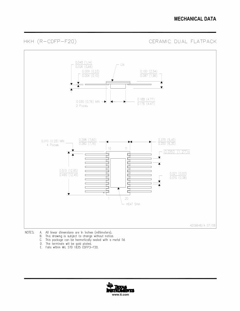
HKH PACKAGE
(TOP VIEW)
NC - No internal connection
1
2
3
4
5
6
7
8
9
10 11
12
13
14
15
16
17
18
19
20VIN1
VIN1
MR2
MR1
EN
SEQ
GND
VIN2
VIN2
NC
NC
VOUT1
VOUT1
VSENSE1
PG1
RESET
VSENSE2
VOUT2
VOUT2
NC
DESCRIPTION
TPS70358M
www.ti.com ...................................................................................................................................................................................................... SLVS759–JUNE 2009
DUAL-OUTPUT LOW-DROPOUT VOLTAGE REGULATORSWITH POWER UP SEQUENCING FOR SPLIT VOLTAGE DSP SYSTEMS
• Two Manual Reset Inputs• Dual Output Voltages for Split-Supply • 2% Accuracy Over Load and Temperature
Applications • Undervoltage Lockout (UVLO) Feature• Selectable Power Up Sequencing for DSP • 20-Pin Ceramic Flatpack Package
Applications • Thermal Shutdown Protection• –55°C to 125°C Operating Temperature• Output Current Range of 1 A on Regulator 1
and 2 A on Regulator 2• Fast Transient Response• Voltage Options Are 3.3 V/2.5 V• Open Drain Power-On Reset With 120-ms
Delay• Open Drain Power Good for Regulator 1• Ultralow 185-µA (typical) Quiescent Current• 2-µA Input Current During Standby• Low Noise: 78-µVRMS Without Bypass
Capacitor• Quick Output Capacitor Discharge Feature
The TPS70358 is designed to provide a complete power management solution for TI DSP, processor power,ASIC, FPGA, and digital applications where dual output voltage regulators are required. Easy programmability ofthe sequencing function makes this family ideal for any TI DSP applications with power sequencing requirement.Differentiated features, such as accuracy, fast transient response, SVS supervisory circuit (power on reset),manual reset inputs, and enable function, provide a complete system solution.
1
Please be aware that an important notice concerning availability, standard warranty, and use in critical applications of TexasInstruments semiconductor products and disclaimers thereto appears at the end of this data sheet.
PRODUCTION DATA information is current as of publication date. Copyright © 2009, Texas Instruments IncorporatedProducts conform to specifications per the terms of the TexasInstruments standard warranty. Production processing does notnecessarily include testing of all parameters.
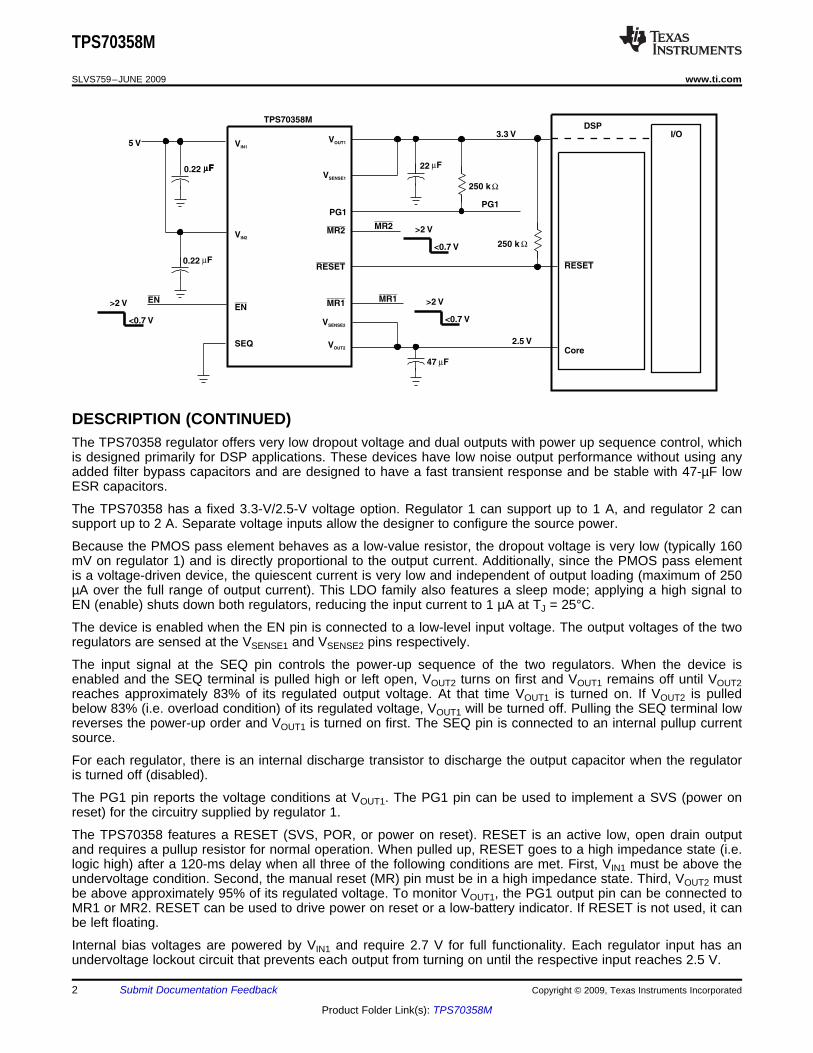
2.5 V
VIN1
VIN2
EN
SEQ
VOUT1
VSENSE1
PG1
MR2
RESET
MR1
VSENSE2
TPS70358M
5 V
3.3 V I/O
MR1
Core
µF
RESET
22
47
0.22
DSP
MR2
PG1
EN
250 k Ω
>2 V
<0.7 V
250 k Ω
>2 V
<0.7 V
>2 V
<0.7 V
VOUT2
0.22 µF µFµF
µF
µF
DESCRIPTION (CONTINUED)
TPS70358M
SLVS759–JUNE 2009 ...................................................................................................................................................................................................... www.ti.com
The TPS70358 regulator offers very low dropout voltage and dual outputs with power up sequence control, whichis designed primarily for DSP applications. These devices have low noise output performance without using anyadded filter bypass capacitors and are designed to have a fast transient response and be stable with 47-µF lowESR capacitors.
The TPS70358 has a fixed 3.3-V/2.5-V voltage option. Regulator 1 can support up to 1 A, and regulator 2 cansupport up to 2 A. Separate voltage inputs allow the designer to configure the source power.
Because the PMOS pass element behaves as a low-value resistor, the dropout voltage is very low (typically 160mV on regulator 1) and is directly proportional to the output current. Additionally, since the PMOS pass elementis a voltage-driven device, the quiescent current is very low and independent of output loading (maximum of 250µA over the full range of output current). This LDO family also features a sleep mode; applying a high signal toEN (enable) shuts down both regulators, reducing the input current to 1 µA at TJ = 25°C.
The device is enabled when the EN pin is connected to a low-level input voltage. The output voltages of the tworegulators are sensed at the VSENSE1 and VSENSE2 pins respectively.
The input signal at the SEQ pin controls the power-up sequence of the two regulators. When the device isenabled and the SEQ terminal is pulled high or left open, VOUT2 turns on first and VOUT1 remains off until VOUT2reaches approximately 83% of its regulated output voltage. At that time VOUT1 is turned on. If VOUT2 is pulledbelow 83% (i.e. overload condition) of its regulated voltage, VOUT1 will be turned off. Pulling the SEQ terminal lowreverses the power-up order and VOUT1 is turned on first. The SEQ pin is connected to an internal pullup currentsource.
For each regulator, there is an internal discharge transistor to discharge the output capacitor when the regulatoris turned off (disabled).
The PG1 pin reports the voltage conditions at VOUT1. The PG1 pin can be used to implement a SVS (power onreset) for the circuitry supplied by regulator 1.
The TPS70358 features a RESET (SVS, POR, or power on reset). RESET is an active low, open drain outputand requires a pullup resistor for normal operation. When pulled up, RESET goes to a high impedance state (i.e.logic high) after a 120-ms delay when all three of the following conditions are met. First, VIN1 must be above theundervoltage condition. Second, the manual reset (MR) pin must be in a high impedance state. Third, VOUT2 mustbe above approximately 95% of its regulated voltage. To monitor VOUT1, the PG1 output pin can be connected toMR1 or MR2. RESET can be used to drive power on reset or a low-battery indicator. If RESET is not used, it canbe left floating.
Internal bias voltages are powered by VIN1 and require 2.7 V for full functionality. Each regulator input has anundervoltage lockout circuit that prevents each output from turning on until the respective input reaches 2.5 V.
2 Submit Documentation Feedback Copyright © 2009, Texas Instruments Incorporated
Product Folder Link(s): TPS70358M

UVLO1
Thermal
Shutdown
Shutdown2.5 V
+-
Current
Sense
Reference Vref
Vref
ENA_1
ENA_1
10 k Ω
Rising Edge
Deglitch0.95 × Vref
FB2Falling Edge
Delay
VIN1
0.95 × Vref
FB1Rising Edge
Deglitch
Falling Edge
Deglitch0.83 × Vref
FB2
UV Comp
Falling Edge
Deglitch0.83 × Vref
FB1
UV Comp
Power
Sequence
Logic
ENA_1
ENA_2
VIN1
Current
Sense
+-
10 k Ω
ENA_2
ENA_2
FB2Vref
V (2 Pins)IN1
GND
EN
SEQ
(see Note B)
V (2 Pins)IN2
V (2 Pins)OUT1
VSENSE1
(see Note A)
PG1
MR2
RESET
MR1
VSENSE2
(see Note A)
V (2 Pins)OUT2
FB1
VIN1
UVLO1
2.5 V UVLO2
Shutdown
NOTES: A. For most applications, V and V should be externally connected to V as close as possible to the device.
For other implementations, refer to SENSE terminal connection discussion in the Application Information section.B. If the SEQ terminal is floating at the input, V powers up first.
SENSE1 SENSE2 OUT
OUT2
TPS70358M
www.ti.com ...................................................................................................................................................................................................... SLVS759–JUNE 2009
ORDERING INFORMATION (1)
VOLTAGE (V) PACKAGE-LEAD ORDERABLE PART TOP-SIDEPRODUCT TJ(DESIGNATOR) NUMBER MARKINGVOUT1 VOUT2
TPS70358M 3.3 V 2.5 V DFP-20 (HKH) –55°C to 125°C TPS70358MHKH TPS70358MHKH
(1) For the most current package and ordering information, see the Package Option Addendum at the end of this document, or see the TIwebsite at www.ti.com.
DETAILED BLOCK DIAGRAM - FIXED VOLTAGE VERSION
Copyright © 2009, Texas Instruments Incorporated Submit Documentation Feedback 3
Product Folder Link(s): TPS70358M
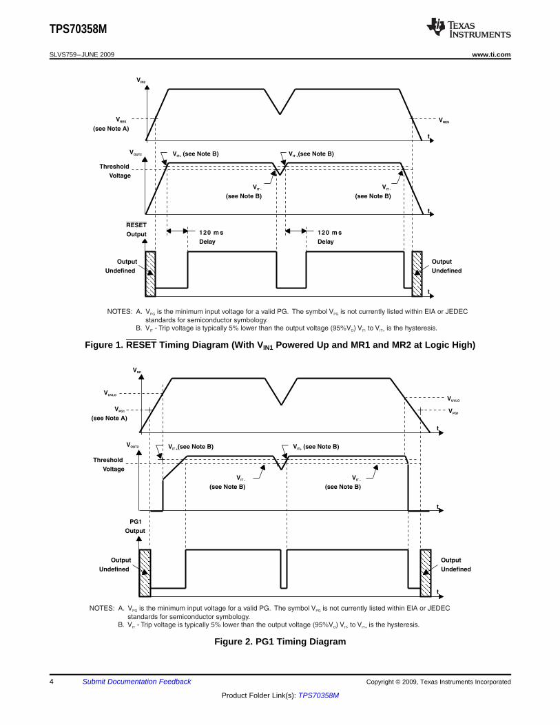
VIN2
VRES
(see Note A)
VRES
t
t
t
VOUT2
Threshold
Voltage
RESET
Output 120 m s
Delay
120 m s
Delay
Output
Undefined
Output
Undefined
V (see Note B)IT +
VIT -
(see Note B)
V (see Note B)IT+
VIT -
(see Note B)
NOTES: A. V is the minimum input voltage for a valid PG. The symbol V is not currently listed within EIA or JEDEC
standards for semiconductor symbology.B. V - Trip voltage is typically 5% lower than the output voltage (95%V ) V to V is the hysteresis.
PG PG
IT O IT- IT+
VPG1
t
t
t
Threshold
Voltage
PG1
Output
Output
Undefined
Output
Undefined
V (see Note B)IT+V (see Note B)IT +
VIN1
VOUT2
VPG1
(see Note A)
VIT -
(see Note B)
VIT -
(see Note B)
VUVLO
VUVLO
NOTES: A. V is the minimum input voltage for a valid PG. The symbol V is not currently listed within EIA or JEDEC
standards for semiconductor symbology.B. V - Trip voltage is typically 5% lower than the output voltage (95%V ) V to V is the hysteresis.
PG PG
IT O IT- IT+
TPS70358M
SLVS759–JUNE 2009 ...................................................................................................................................................................................................... www.ti.com
Figure 1. RESET Timing Diagram (With VIN1 Powered Up and MR1 and MR2 at Logic High)
Figure 2. PG1 Timing Diagram
4 Submit Documentation Feedback Copyright © 2009, Texas Instruments Incorporated
Product Folder Link(s): TPS70358M
DETAILED DESCRIPTION
PIN FUNCTIONS
TPS70358M
www.ti.com ...................................................................................................................................................................................................... SLVS759–JUNE 2009
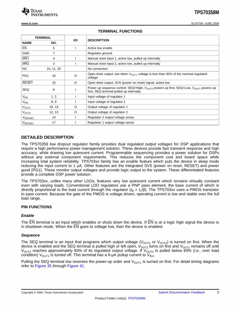
TERMINAL FUNCTIONSTERMINAL
I/O DESCRIPTIONNAME NO.EN 5 I Active low enableGND 7 Regulator groundMR1 4 I Manual reset input 1, active low, pulled up internallyMR2 3 I Manual reset input 2, active low, pulled up internallyNC 10, 11, 20 No connection
Open drain output, low when VOUT1 voltage is less than 95% of the nominal regulatedPG1 16 O voltageRESET 15 O Open drain output, SVS (power on reset) signal, active low
Power up sequence control: SEQ=High, VOUT2 powers up first; SEQ=Low, VOUT1 powers upSEQ 6 I first, SEQ terminal pulled up internally.VIN1 1, 2 I Input voltage of regulator 1VIN2 8, 9 I Input voltage of regulator 2VOUT1 18, 19 O Output voltage of regulator 1VOUT2 12, 13 O Output voltage of regulator 2VSENSE2 14 I Regulator 2 output voltage senseVSENSE1 17 I Regulator 1 output voltage sense
The TPS70358 low dropout regulator family provides dual regulated output voltages for DSP applications thatrequire a high performance power management solution. These devices provide fast transient response and highaccuracy, while drawing low quiescent current. Programmable sequencing provides a power solution for DSPswithout any external component requirements. This reduces the component cost and board space whileincreasing total system reliability. TPS703xx family has an enable feature which puts the device in sleep modereducing the input current to 1 µA. Other features are the integrated SVS (power on reset, RESET) and powergood (PG1). These monitor output voltages and provide logic output to the system. These differentiated featuresprovide a complete DSP power solution.
The TPS703xx, unlike many other LDOs, features very low quiescent current which remains virtually constanteven with varying loads. Conventional LDO regulators use a PNP pass element, the base current of which isdirectly proportional to the load current through the regulator (IB = IC/β). The TPS703xx uses a PMOS transistorto pass current. Because the gate of the PMOS is voltage driven, operating current is low and stable over the fullload range.
EnableThe EN terminal is an input which enables or shuts down the device. If EN is at a logic high signal the device isin shutdown mode. When the EN goes to voltage low, then the device is enabled.
SequenceThe SEQ terminal is an input that programs which output voltage (VOUT1 or VOUT2) is turned on first. When thedevice is enabled and the SEQ terminal is pulled high or left open, VOUT2 turns on first and VOUT1 remains off untilVOUT2 reaches approximately 83% of its regulated output voltage. If VOUT2 is pulled below 83% (i.e., over loadcondition) VOUT1 is turned off. This terminal has a 6-µA pullup current to VIN1.
Pulling the SEQ terminal low reverses the power-up order and VOUT1 is turned on first. For detail timing diagramsrefer to Figure 35 through Figure 41.
Copyright © 2009, Texas Instruments Incorporated Submit Documentation Feedback 5
Product Folder Link(s): TPS70358M
TPS70358M
SLVS759–JUNE 2009 ...................................................................................................................................................................................................... www.ti.com
Power Good (PG1)The PG1 terminal is an open drain, active high output terminal which indicates the status of the VOUT1 regulator.When the VOUT1 reaches 95% of its regulated voltage, PG1 goes to a high impedance state. PG1 goes to a lowimpedance state when VOUT1 is pulled below 95% (i.e., over load condition) of its regulated voltage. The opendrain output of the PG1 terminal requires a pullup resistor.
Manual Reset Pins (MR1 and MR2)MR1 and MR2 are active low input terminals used to trigger a reset condition. When either MR1 or MR2 is pulledto logic low, a POR (RESET) occurs. These terminals have a 6-µA pullup current to VIN1. It is recommended thatthese pins be pulled high to VIN when they are not used.
Sense (VSENSE1, VSENSE2
The sense terminals of fixed-output options must be connected to the regulator output, and the connectionshould be as short as possible. Internally, the sense terminals connect to high-impedance wide-bandwidthamplifiers through resistor-divider networks and noise pickup feeds through to the regulator output. It is essentialto route the sense connections in such a way to minimize/avoid noise pickup. Adding RC networks between theVSENSE terminals and VOUT terminals to filter noise is not recommended because it can cause the regulators tooscillate.
RESET IndicatorRESET is an active low, open drain output and requires a pullup resistor for normal operation. When pulled up,RESET goes to a high impedance state (i.e. logic high) after a 120-ms delay when all three of the followingconditions are met. First, VIN1 must be above the undervoltage condition. Second, the manual reset (MR) pinmust be in a high impedance state. Third, VOUT2 must be above approximately 95% of its regulated voltage. Tomonitor VOUT1, the PG1 output pin can be connected to MR1 or MR2.
VIN1 and VIN2
VIN1 and VIN2 are inputs to the regulators.
VOUT1 and VOUT2
VOUT1 and VOUT2 are output terminals of each regulator.
6 Submit Documentation Feedback Copyright © 2009, Texas Instruments Incorporated
Product Folder Link(s): TPS70358M
ABSOLUTE MAXIMUM RATINGS (1)
RECOMMENDED OPERATING CONDITIONS
ELECTRICAL CHARACTERISTICS
TPS70358M
www.ti.com ...................................................................................................................................................................................................... SLVS759–JUNE 2009
over operating free-air temperature range (unless otherwise noted)
VALUE UNITVIN1, VIN2 Input voltage range (2) –0.3 to 7 V
Voltage range at EN –0.3 to 7 VVOUT1,VSENSE1, Output violtage range 5.5 VVOUT2,VSENSE2
Maximum RESET, PG1 voltage 7 VMaximum MR1, MR2 and SEQ voltage VIN1
Peak output current Internally limitedTJ Operating virtual junction temperature range –55 to 150 °C
θJC (die to package top) 17.2Package thermal impedance θJC (die to package bottom) 5.49 °C/W
θJB (die to standard PCB trace) 38.4Tstg Storage temperature range –65 to 150 °C
ESD rating (HBM, human body model) 2 kV
(1) Stresses beyond those listed under “absolute maximum ratings” may cause permanent damage to the device. These are stress ratingsonly, and functional operation of the device at these or any other conditions beyond those indicated under “recommended operatingconditions” is not implied. Exposure to absolute-maximum-rated conditions for extended periods may affect device reliability.
(2) All voltages are tied to network ground.
over operating free-air temperature range (unless otherwise noted)
MIN NOM MAX UNITVI Input voltage (1) 2.7 6 V
Regulator 1 0 1IO Output current A
Regulator 2 0 2TJ Operating virtual storage temperature –55 125 °C
(1) To calculate the minimum input voltage for maximum output current, use the following equation: VI(min) = VO(max) + VDO(max load).
over operating junction temperature range (TJ = –55°C to 125°C) VIN1 or VIN2 = VOUTX(nom) + V, IOUTX = 1 mA, EN = 0,COUT1 = 22 µF, COUT2 = 47 µF (unless otherwise noted)
PARAMETER TEST CONDITIONS MIN TYP MAX UNIT3.5 V < VI < 6 V, TJ = 25°C 2.52.5 V output
(VOUT2) 3.5 V < VI < 6 V 2.45 2.55VO Output voltage (1) (2) V
4.3 V < VI < 6 V, TJ = 25°C 3.33.3 V output(VOUT1) 4.3 V < VI < 6 V 3.234 3.366
TJ = 25°C 185Quiescent current (GND current) for regulator 1 µAand regulator 2, EN = 0 V (2) (1) 250Load regulation for VOUT1 and VOUT2
(3) TJ = 25°C 1 mVOuput voltage line regulationfor regulator 1 and regulator VO + 1 V < VI < 6 V, TJ = 25°C 0.01%2 (1)
mVRegulator 1 5.6
VO + 1 V < VI < 6 V,Regulator 2 6.25
(1) Minimum input operating voltage is 2.7 V or VO(typ) + 1 V, whichever is greater. Maximum input voltage = 6 V, minimum output current is1 mA.
(2) Input voltage(VIN1 or VIN2) = VO(Typ) − 100 mV. For the 2.5-V regulators, the dropout voltage is limited by input voltage range. The3.3-V regulator input voltage is set to 3.2 V to perform this test.
(3) IO = 1 mA to 1 A for regulator 1 and 1 mA to 2 A for regulator 2.
Copyright © 2009, Texas Instruments Incorporated Submit Documentation Feedback 7
Product Folder Link(s): TPS70358M
TPS70358M
SLVS759–JUNE 2009 ...................................................................................................................................................................................................... www.ti.com
ELECTRICAL CHARACTERISTICS (continued)over operating junction temperature range (TJ = –55°C to 125°C) VIN1 or VIN2 = VOUTX(nom) + V, IOUTX = 1 mA, EN = 0,COUT1 = 22 µF, COUT2 = 47 µF (unless otherwise noted)
PARAMETER TEST CONDITIONS MIN TYP MAX UNITRegulator 1 1.75 2.2
Ouput current limit VO = 0 V ARegulator 2 3.8 4.5
Thermal shutdown junction temperature 150 °CEN = VI, TJ = 25°C 1 2
II(standby) Standby current µAEN = VI 10
RESET TERMINALMinimum input voltage for valid RESET I(RESET) = 300 µA, V(RESET) ≤ 0.8 V 1 1.45 VTrip threshold voltage VO decreasing 92% 95% 98% VO
Hysteresis voltage Measured at VO 0.5% VO
RESET pulset(RESET)(4) TJ = 25°C 80 120 160 msduration
tr(RESET)(4) Rising edge deglitch 30 µs
Output low voltage VI = 3.5 V, I(RESET) = 1 mA 0.15 0.4 VLeakage current V(RESET) = 6 V 1 µAPG TERMINALMinimum input voltage for valid PG I(PG) = 300 µA, V(PG1) ≤ 0.8 V 1 1.45 VTrip threshold voltage VO decreasing 92% 95% 98% VO
Hysteresis voltage Measured at VO 0.5% VO
tr(PG1) Rising edge deglitch 30 µsOutput low voltage VI = 2.7 V, I(PG) = 1 mA 0.15 0.4 VLeakage current V(PG1) = 6 V 1 µAEN TERMINALHigh–level EN input voltage 2 VLow–level EN input voltage 0.7 VInput current (EN) -1 1 µASEQ TERMINALHigh–level SEQ input voltage 2 VLow–level SEQ input voltage 0.7 VSEQ pullup current source 6 µAMR1 / MR2 TERMINALHigh–level input voltage 2 VLow–level input voltage 0.7 VPullup current source 6 µAVOUT2 TERMINALVOUT2 UV comparator - positive–going input 80% VO 83% VO 86% VO Vthreshold voltage of VOUT2 UV comparatorVOUT2 UV comparator - hysteresis 3% VO mVVOUT2 UV comparator - falling edge deglitch (4) VSENSE2 decreasing below threshold 140 µsPeak output current 2-ms pulse width 3 ADischarge transistor current VOUT2 = 1.5 V 7.5 mAVOUT1 TERMINALVOUT1 UV comparator - positive–going input 80% VO 83% VO 86% VO Vthreshold voltage of VOUT1 UV comparatorVOUT1 UV comparator - hysteresis 3% VO mVVOUT1 UV comparator - falling edge deglitch VSENSE1 decreasing below threshold 140 µs
(4) Not production tested. Specified by design.
8 Submit Documentation Feedback Copyright © 2009, Texas Instruments Incorporated
Product Folder Link(s): TPS70358M
TPS70358M
www.ti.com ...................................................................................................................................................................................................... SLVS759–JUNE 2009
ELECTRICAL CHARACTERISTICS (continued)over operating junction temperature range (TJ = –55°C to 125°C) VIN1 or VIN2 = VOUTX(nom) + V, IOUTX = 1 mA, EN = 0,COUT1 = 22 µF, COUT2 = 47 µF (unless otherwise noted)
PARAMETER TEST CONDITIONS MIN TYP MAX UNITIO = 1 A, VIN1 = 3.2 V, TJ = 25C 160
Dropout voltage (5) mVIO = 1 A, VIN1 = 3.2 V 400
Peak output current 2-ms pulse width 1.2 ADischarge transistor current VOUT1 = 1.5 V 7.5 mAVIN1 / VIN2 TERMINALUVLO threshold 2.3 2.65 VUVLO hysteresis 110 mV
(5) Input voltage(VIN1 or VIN2) = VO(Typ) − 100 mV. For the 2.5-V regulators, the dropout voltage is limited by input voltage range. The3.3-V regulator input voltage is set to 3.2 V to perform this test.
Copyright © 2009, Texas Instruments Incorporated Submit Documentation Feedback 9
Product Folder Link(s): TPS70358M
TYPICAL CHARACTERISTICS
3.27
3.28
3.29
3.30
3.31
0 200 400 600 800 1000
IO - O utput C urrent - m A
-O
utp
ut
Vo
lta
ge
-V
VO
V = 4.3 VIN1
T = 25J ° C
VOUT1
3.32
3.33
1.785
1.79
1.795
1.8
1.805
0 500 1000 1500 2000
IO - O utput C urrent - m A
-O
utp
ut
Vo
lta
ge
-V
VO
V = 2.8VIN2
T = 25J °C
VOUT2
1.81
1.815
TPS70358M
SLVS759–JUNE 2009 ...................................................................................................................................................................................................... www.ti.com
Table 1. TPS70358MVOLTAGE (V) SPECIFIEDPACKAGE-LEAD ORDERING TOP-SIDEPRODUCT TEMPERATURE(DESIGNATOR) NUMBER MARKINGVOUT1 VOUT2 RANGE (TJ)
TPS70358M 3.3 V 2.5 V DFP-20 (HKH) –55°C to 125°C TPS70358MHKH TPS70358MHKH
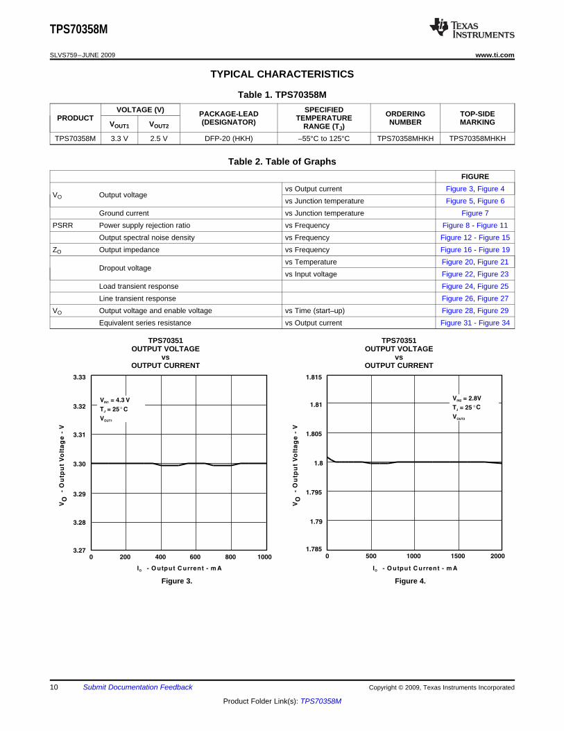
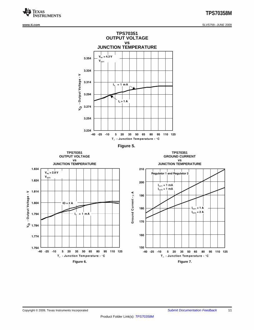
Table 2. Table of GraphsFIGURE
vs Output current Figure 3, Figure 4VO Output voltage
vs Junction temperature Figure 5, Figure 6Ground current vs Junction temperature Figure 7
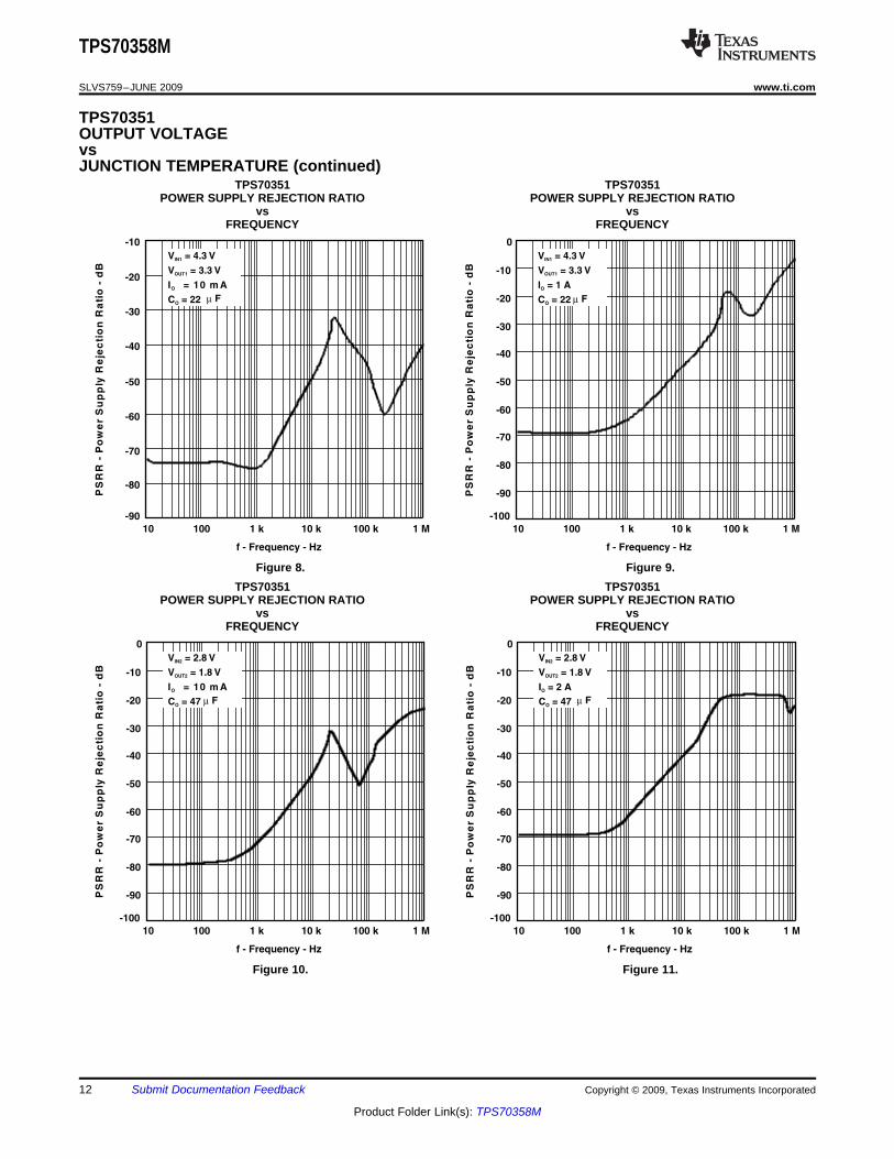
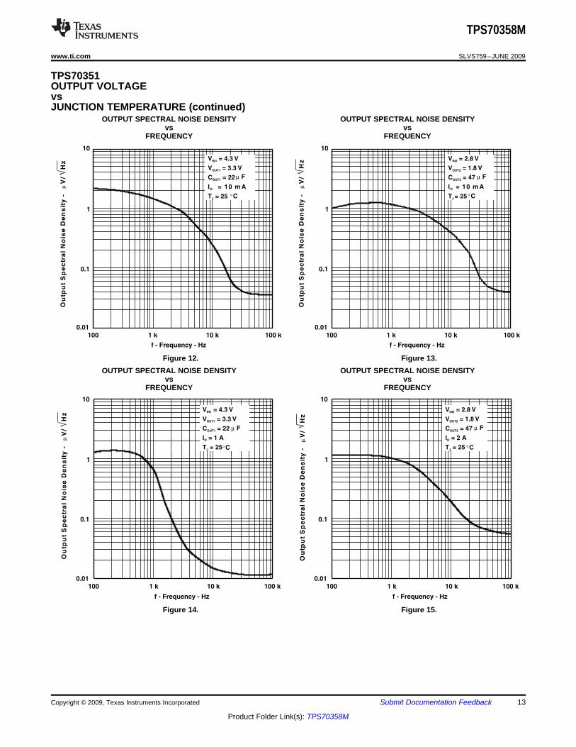
PSRR Power supply rejection ratio vs Frequency Figure 8 - Figure 11Output spectral noise density vs Frequency Figure 12 - Figure 15
ZO Output impedance vs Frequency Figure 16 - Figure 19vs Temperature Figure 20, Figure 21
Dropout voltagevs Input voltage Figure 22, Figure 23
Load transient response Figure 24, Figure 25Line transient response Figure 26, Figure 27
VO Output voltage and enable voltage vs Time (start–up) Figure 28, Figure 29Equivalent series resistance vs Output current Figure 31 - Figure 34
TPS70351 TPS70351OUTPUT VOLTAGE OUTPUT VOLTAGE
vs vsOUTPUT CURRENT OUTPUT CURRENT
Figure 3. Figure 4.
10 Submit Documentation Feedback Copyright © 2009, Texas Instruments Incorporated
Product Folder Link(s): TPS70358M
TPS70351
-40 -25 -10 5 20 35 50 65 80 95 110 125
3.234
3.254
3.274
3.294
3.314
3.334
3.354
T J - Junction Tem perature - °C
-O
utp
ut
Vo
lta
ge
-V
VO
V = 4.3 VIN1
VOUT1
I = 1 AO
IO = 1 m A
1.764
1.774
1.784
1.794
1.804
1.814
1.824
1.834
T J - Junction Tem perature - °C
-O
utp
ut
Vo
lta
ge
-V
VO
-40 -25 -10 5 20 35 50 65 80 95 110 125
IO = 1 m A
IO = 2 A
V = 2.8 VIN2
VOUT2
150
160
170
180
190
200
T J - Junction Tem perature - °C
Gro
un
dC
urr
en
t-
Aµ
-40 -25 -10 5 20 35 50 65 80 95 110 125
210
Regulator 1 and Regulator 2
I = 1 AOUT1
I = 2 AOUT2
I = 1 mAOUT1
I = 1 mAOUT2
TPS70358M
www.ti.com ...................................................................................................................................................................................................... SLVS759–JUNE 2009
OUTPUT VOLTAGEvs
JUNCTION TEMPERATURE
Figure 5.TPS70351 TPS70351
OUTPUT VOLTAGE GROUND CURRENTvs vs
JUNCTION TEMPERATURE JUNCTION TEMPERATURE
Figure 6. Figure 7.
Copyright © 2009, Texas Instruments Incorporated Submit Documentation Feedback 11
Product Folder Link(s): TPS70358M
-50
-60
-80
-90
10 100 1 k 10 k
PS
RR
-P
ow
er
Su
pp
lyR
eje
cti
on
Ra
tio
-d
B
-30
-20
f - Frequency - Hz
-10
100 k 1 M
-40
-70
V = 4.3 VIN1
V = 3.3 VOUT1
IO = 10 m A
C = 22Oµ F
PS
RR
-P
ow
er
Su
pp
lyR
eje
cti
on
Ra
tio
-d
B
-50
-60
-80
-100
-20
-10
0
-30
-40
-70
-90
10 100 1 k 10 k
f - Frequency - Hz
100 k 1 M
V = 4.3 VIN1
V = 3.3 VOUT1
I = 1 AO
C = 22Oµ F
-50
-60
-80
-100
-20
-10
0
-30
-40
-70
-90
10 100 1 k 10 k
PS
RR
-P
ow
er
Su
pp
lyR
eje
cti
on
Ra
tio
-d
B
f - Frequency - Hz
100 k 1 M
V = 2.8 VIN2
V = 1.8 VOUT2
IO = 10 m A
C = 47Oµ F
-50
-60
-80
-100
-20
-10
0
-30
-40
-70
-90
10 100 1 k 10 k
PS
RR
-P
ow
er
Su
pp
lyR
eje
cti
on
Ra
tio
-d
B
f - Frequency - Hz
100 k 1 M
V = 2.8 VIN2
V = 1.8 VOUT2
I = 2 AO
C = 47Oµ F
TPS70358M
SLVS759–JUNE 2009 ...................................................................................................................................................................................................... www.ti.com
TPS70351OUTPUT VOLTAGEvsJUNCTION TEMPERATURE (continued)
TPS70351 TPS70351POWER SUPPLY REJECTION RATIO POWER SUPPLY REJECTION RATIO
vs vsFREQUENCY FREQUENCY
Figure 8. Figure 9.TPS70351 TPS70351
POWER SUPPLY REJECTION RATIO POWER SUPPLY REJECTION RATIOvs vs
FREQUENCY FREQUENCY
Figure 10. Figure 11.
12 Submit Documentation Feedback Copyright © 2009, Texas Instruments Incorporated
Product Folder Link(s): TPS70358M
0.01
0.1
1
10
100 1 k 10 k 100 k
f - Frequency - Hz
V/
Hz
Ou
tpu
tS
pe
ctr
al
No
ise
De
ns
ity
-µ
V = 4.3 VIN1
V = 3.3 VOUT1
C = 22OUT1µ F
IO = 10 m A
T = 25J °C
0.01
0.1
1
10
100 1 k 10 k 100 k
f - Frequency - Hz
V/
Hz
Ou
tpu
tS
pe
ctr
al
No
ise
De
ns
ity
-µ
V = 2.8 VIN2
V = 1.8 VOUT2
C = 47OUT2µ F
IO = 10 m A
T = 25J °C
0.01
0.1
1
10
100 1 k 10 k 100 k
f - Frequency - Hz
V = 4.3 VIN1
V = 3.3 VOUT1
C = 22OUT1 µ F
I = 1 AO
T = 25J °C
V/
Hz
Ou
tpu
tS
pe
ctr
al
No
ise
De
ns
ity
-µ
0.01
0.1
1
10
100 1 k 10 k 100 k
f - Frequency - Hz
V = 2.8 VIN2
V = 1.8 VOUT2
C = 47OUT2µ F
I = 2 AO
T = 25J °C
V/
Hz
Ou
tpu
tS
pe
ctr
al
No
ise
De
ns
ity
-µ
TPS70358M
www.ti.com ...................................................................................................................................................................................................... SLVS759–JUNE 2009
TPS70351OUTPUT VOLTAGEvsJUNCTION TEMPERATURE (continued)
OUTPUT SPECTRAL NOISE DENSITY OUTPUT SPECTRAL NOISE DENSITYvs vs
FREQUENCY FREQUENCY
Figure 12. Figure 13.OUTPUT SPECTRAL NOISE DENSITY OUTPUT SPECTRAL NOISE DENSITY
vs vsFREQUENCY FREQUENCY
Figure 14. Figure 15.
Copyright © 2009, Texas Instruments Incorporated Submit Documentation Feedback 13
Product Folder Link(s): TPS70358M
0.1
0.01
10 100 1 k 10 k
-O
utp
ut
Imp
ed
an
ce
- 1
f - Frequency - Hz
100 k 1 M 10 M
ZO
Ω
V = 3.3 VOUT1
IO = 10 m A
C = 22Oµ F
0.1
0.01
10 100 1 k 10 k
-O
utp
ut
Imp
ed
an
ce
- 1
f - Frequency - Hz
100 k 1 M 10 M
ZO
Ω
V = 3.3 VOUT1
I = 1 AO
C = 22O µ F
0.1
0.01
10 100 1 k 10 k
-O
utp
ut
Imp
ed
an
ce
- 1
f - Frequency - Hz
100 k 1 M 10 M
ZO
Ω
V = 1.8 VOUT2
IO = 10 m A
C = 47Oµ F
0.1
0.01
10 100 1 k 10 k
-O
utp
ut
Imp
ed
an
ce
- 1
f - Frequency - Hz
100 k 1 M 10 M
ZO
Ω
V = 1.8 VOUT2
I = 2 AO
C = 47Oµ F
TPS70358M
SLVS759–JUNE 2009 ...................................................................................................................................................................................................... www.ti.com
TPS70351OUTPUT VOLTAGEvsJUNCTION TEMPERATURE (continued)
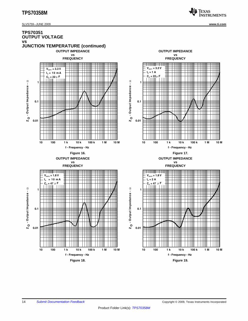
OUTPUT IMPEDANCE OUTPUT IMPEDANCEvs vs
FREQUENCY FREQUENCY
Figure 16. Figure 17.OUTPUT IMPEDANCE OUTPUT IMPEDANCE
vs vsFREQUENCY FREQUENCY
Figure 18. Figure 19.
14 Submit Documentation Feedback Copyright © 2009, Texas Instruments Incorporated
Product Folder Link(s): TPS70358M
-40 -25 -10 5 20 35 50 65 80 95 110 125
0
50
100
150
200
250
T - Tem perature - °C
Dro
po
ut
Vo
lta
ge
-m
V
I = 1 AO
VOUT1
V = 3.2 VIN1
0
5
10
15
20
25
T - Tem perature - °C
Dro
po
ut
Vo
lta
ge
-m
V
-40 -25 -10 5 20 35 50 65 80 95 110 125
IO = 100 m A
IO = 10 m A
IO = 1 m A
VOUT1
V = 3.2 VIN1
0
50
100
150
200
250
2.5 3 3.5 4 4.5 5 5.5
V - Input Voltage - VI
Dro
po
ut
Vo
lta
ge
-m
V
VOUT1
I = 1 AO
300
T = 125J °C
T = 25J °C
T = - 40J °C
0
50
100
150
200
250
2.5 3 3.5 4 4.5 5 5.5
V - Input Voltage - VI
Dro
po
ut
Vo
lta
ge
-m
V
VOUT2
I = 2 AO
300
T = 125J °C
T = 25J °C
T = - 40J °C
TPS70358M
www.ti.com ...................................................................................................................................................................................................... SLVS759–JUNE 2009
TPS70351OUTPUT VOLTAGEvsJUNCTION TEMPERATURE (continued)
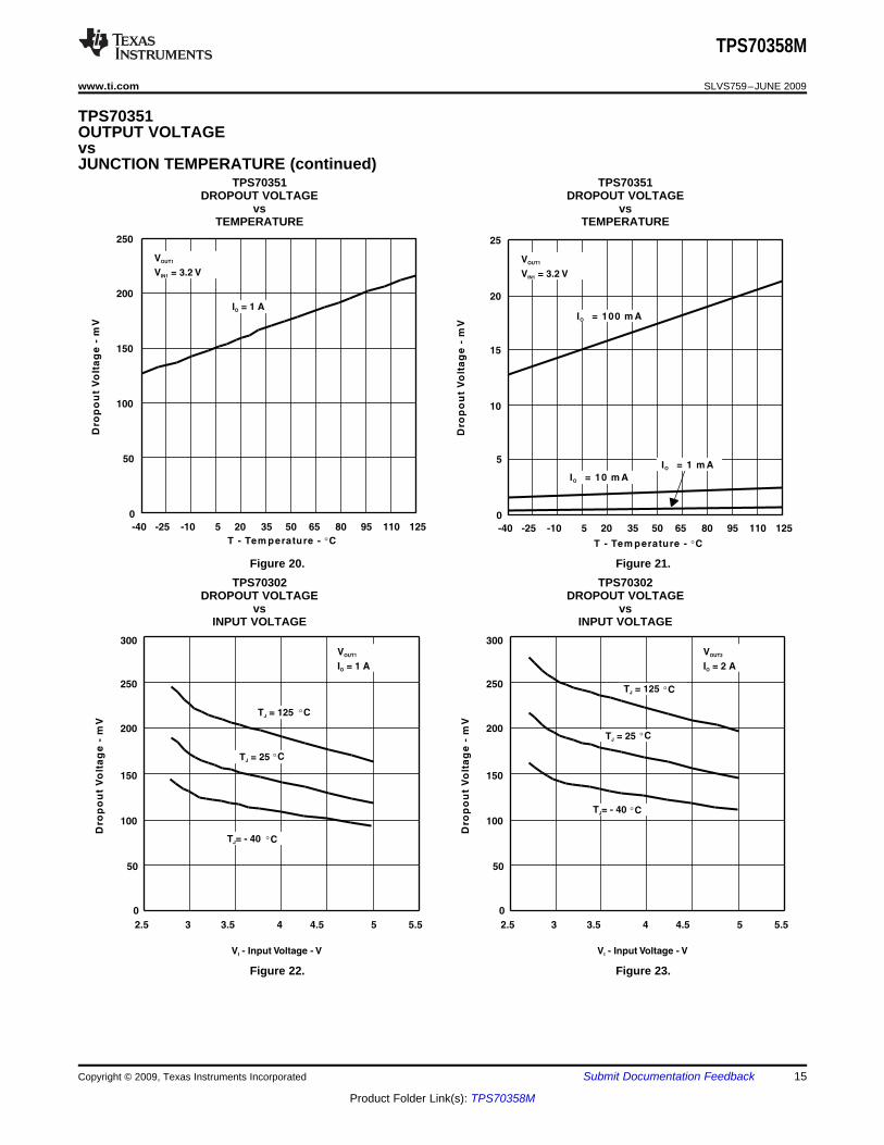
TPS70351 TPS70351DROPOUT VOLTAGE DROPOUT VOLTAGE
vs vsTEMPERATURE TEMPERATURE
Figure 20. Figure 21.TPS70302 TPS70302
DROPOUT VOLTAGE DROPOUT VOLTAGEvs vs
INPUT VOLTAGE INPUT VOLTAGE
Figure 22. Figure 23.
Copyright © 2009, Texas Instruments Incorporated Submit Documentation Feedback 15
Product Folder Link(s): TPS70358M
0 0.2 0.4 0.6 0.8 1 1.2 1.4 1.6 1.8 2
0
0.5
-O
utp
ut
Cu
rre
nt
-A
VO
-C
ha
ng
ein
∆
Ou
tpu
tV
olt
ag
e-
mV
I O
t - T im e - m s
V = 4.3 VIN1
V = 3.3 VOUT1
C = 22Oµ F
T = 25J°C
0
-50
-100
1
50
0 0.2 0.4 0.6 0.8 1 1.2 1.4 1.6 1.8 2
50
0
-O
utp
ut
Cu
rre
nt
-A
VO
-C
ha
ng
ein
∆
Ou
tpu
tV
olt
ag
e-
mV
I O
t - T im e - m s
1
0
-50
V = 2.5 VOUT2
I = 2 AO
C = 47Oµ F
T = 25J °C
2
0 20 40 60 80 100 120 140 160 180 200
50
-In
pu
tV
olt
ag
e-
V
VO
-C
ha
ng
ein
∆
Ou
tpu
tV
olt
ag
e-
mV
VI
t - T im e - µs
V = 3.3 VOUT1
I = 1 AO
C = 22Oµ F
4.3
0
-50
5.3
-1000 20 40 60 80 100 120 140 160 180 200
100
-In
pu
tV
olt
ag
e-
V
VO
-C
ha
ng
ein
∆
Ou
tpu
tV
olt
ag
e-
mV
VI
t - T im e - µ s
V = 2.5 VOUT2
I = 2 AO
C = 47Oµ F
2.8
0
-100
3.8
-200
TPS70358M
SLVS759–JUNE 2009 ...................................................................................................................................................................................................... www.ti.com
TPS70351OUTPUT VOLTAGEvsJUNCTION TEMPERATURE (continued)
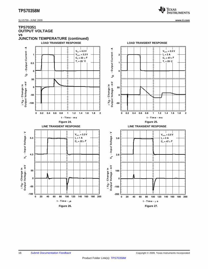
LOAD TRANSIENT RESPONSE LOAD TRANSIENT RESPONSE
Figure 24. Figure 25.LINE TRANSIENT RESPONSE LINE TRANSIENT RESPONSE
Figure 26. Figure 27.
16 Submit Documentation Feedback Copyright © 2009, Texas Instruments Incorporated
Product Folder Link(s): TPS70358M

t - T im e (Start-U p) - m s
0 2
3
1
0
0
5
0.2 1.81.61.41.210.4 0.6 0.8
-O
utp
ut
Vo
lta
ge
-V
VO
En
ab
leV
olt
ag
e-
V
V = 3.3 VOUT1
I = 1 AO
C = 22Oµ F
V = 4.3 VIN1
SEQ = Low
2
4
t - T im e (Start-U p) - m s
0 2
2
1
0
0
5
0.2 1.81.61.41.210.4 0.6 0.8
-O
utp
ut
Vo
lta
ge
-V
VO
En
ab
leV
olt
ag
e-
V
V = 1.8 VOUT2
I = 2 AO
C = 47Oµ F
V = 2.8 VIN2
SEQ = High
IN
EN
OUT
+
GND
CO
ESR
RL
VI
To Load
TPS70358M
www.ti.com ...................................................................................................................................................................................................... SLVS759–JUNE 2009
TPS70351OUTPUT VOLTAGEvsJUNCTION TEMPERATURE (continued)
OUTPUT VOLTAGE AND ENABLE VOLTAGE OUTPUT VOLTAGE AND ENABLE VOLTAGEvs vs
TIME (START-UP) TIME (START-UP)
Figure 28. Figure 29.
Figure 30. Test Circuit for Typical Regions of Stability
Copyright © 2009, Texas Instruments Incorporated Submit Documentation Feedback 17
Product Folder Link(s): TPS70358M

I - Output Current - AO
ES
R-
Eq
uiv
ale
nt
Se
rie
sR
es
ista
nc
e-
Ω
0.1
0.01
10
1
0 0.2
REGION OF INSTABILITY
0.1 0.3 0.4 0.5 0.6 0.7 0.8 0.9 1
V = 3.3 VOUT1
C = 22Oµ F
50 m Ω
I - Output Current - AO
ES
R-
Eq
uiv
ale
nt
Se
rie
sR
es
ista
nc
e-
Ω
0.1
0.01
10
1
0 0.2
REGION OF INSTABILITY
0.1 0.3 0.4 0.5 0.6 0.7 0.8 0.9 1
V = 3.3 VOUT1
C = 220Oµ F
15 m Ω
0.1
0.01
10
1
I - Output Current - AO
ES
R-
Eq
uiv
ale
nt
Se
rie
sR
es
ista
nc
e-
Ω
0 0.2
REGION OF INSTABILITY
0.1 0.3 0.4 0.5 0.6 0.7 0.8 0.9 1
50 m Ω
V = 1.8 VOUT2
C = 47Oµ F
0.1
0.01
10
1
I - Output Current - AO
ES
R-
Eq
uiv
ale
nt
Se
rie
sR
es
ista
nc
e-
Ω
0 0.20.1 0.3 0.4 0.5 0.6 0.7 0.8 0.9 1
REGION OF INSTABILITY
V = 1.8 VOUT2
C = 680Oµ F
15 m Ω
TPS70358M
SLVS759–JUNE 2009 ...................................................................................................................................................................................................... www.ti.com
TYPICAL REGION OF STABILITY TYPICAL REGION OF STABILITYEQUIVALENT SERIES RESISTANCE (ESR)(1) EQUIVALENT SERIES RESISTANCE (ESR)(1)
vs vsOUTPUT CURRENT OUTPUT CURRENT
Figure 31. Figure 32.TYPICAL REGION OF STABILITY TYPICAL REGION OF STABILITY
EQUIVALENT SERIES RESISTANCE (ESR)(1) EQUIVALENT SERIES RESISTANCE (ESR)(1)
vs vsOUTPUT CURRENT OUTPUT CURRENT
Figure 33. Figure 34.
18 Submit Documentation Feedback Copyright © 2009, Texas Instruments Incorporated
Product Folder Link(s): TPS70358M
APPLICATION INFORMATION
Sequencing Timing Diagrams
SEQ = Low
VOUT2
VIN1
VIN2
EN
SEQ
VOUT1
VSENSE1
PG1
MR2
RESET
MR1
VSENSE2
VOUT2
TPS70358
(Fixed Output Option)
VI
VOUT1
MR1
0.22 µ F
RESET
22 µ F
47 µ F
0.22
MR2
EN>2 V
<0.7 V
250 k Ω
VIN
µ F
TPS70358M
www.ti.com ...................................................................................................................................................................................................... SLVS759–JUNE 2009
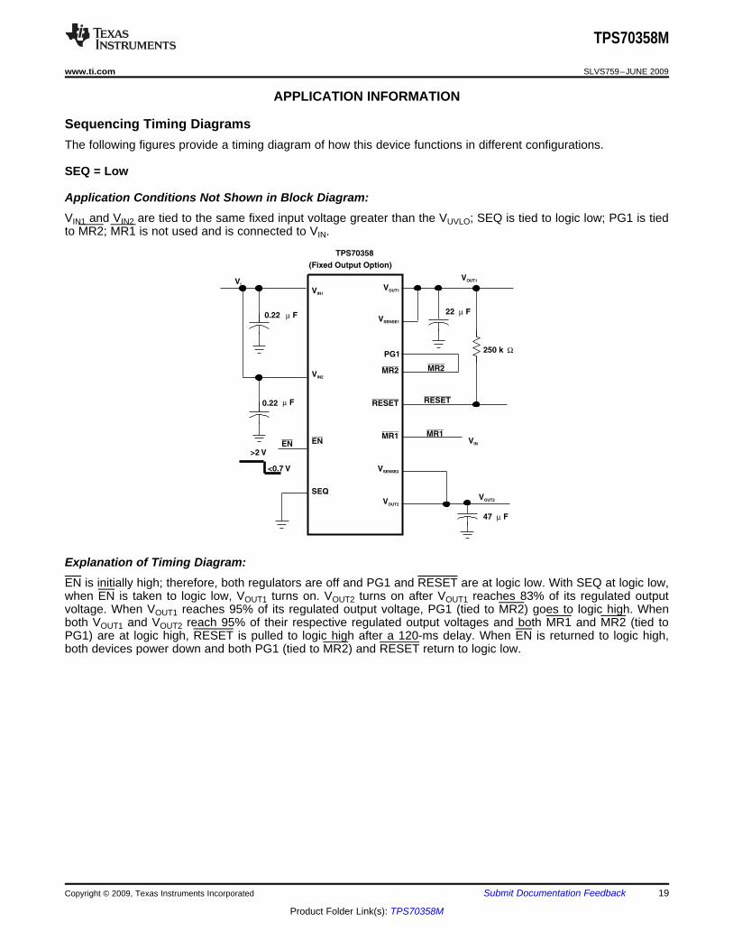
The following figures provide a timing diagram of how this device functions in different configurations.
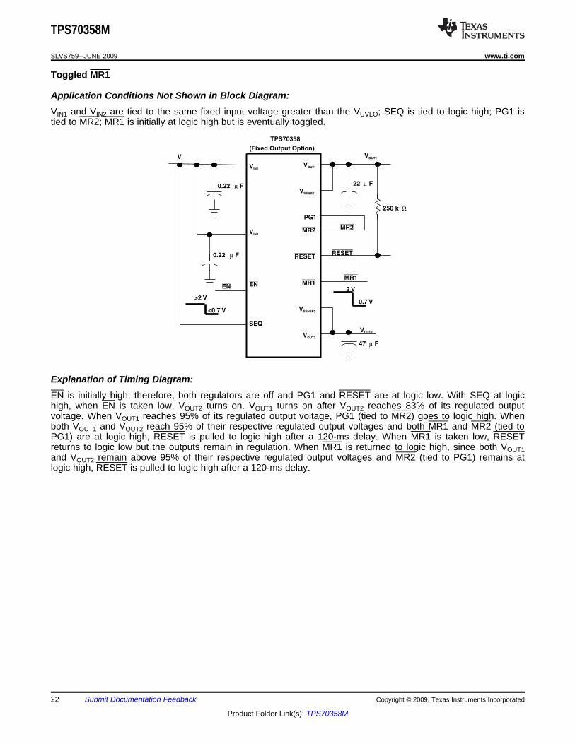
Application Conditions Not Shown in Block Diagram:VIN1 and VIN2 are tied to the same fixed input voltage greater than the VUVLO; SEQ is tied to logic low; PG1 is tiedto MR2; MR1 is not used and is connected to VIN.
Explanation of Timing Diagram:EN is initially high; therefore, both regulators are off and PG1 and RESET are at logic low. With SEQ at logic low,when EN is taken to logic low, VOUT1 turns on. VOUT2 turns on after VOUT1 reaches 83% of its regulated outputvoltage. When VOUT1 reaches 95% of its regulated output voltage, PG1 (tied to MR2) goes to logic high. Whenboth VOUT1 and VOUT2 reach 95% of their respective regulated output voltages and both MR1 and MR2 (tied toPG1) are at logic high, RESET is pulled to logic high after a 120-ms delay. When EN is returned to logic high,both devices power down and both PG1 (tied to MR2) and RESET return to logic low.
Copyright © 2009, Texas Instruments Incorporated Submit Documentation Feedback 19
Product Folder Link(s): TPS70358M

83%
95%
120 ms
EN
VOUT2
VOUT1
PG1
MR1
MR2
( tied to PG1)MR2
RESET
SEQ
95%
83%
NOTE A: t1 - Time at which both V and V are greater than the PG thresholds and is logic high.OUT1 OUT2 MR1
t1
(see Note A)
SEQ = High
RESET
VOUT2
VIN1
VIN2
EN
SEQ
VOUT1
VSENSE1
PG1
MR2
RESET
MR1
VSENSE2
VOUT2
VI
VIN
MR1
0.22 µ F 22 µ F
47 µ F
0.22 µ F
MR2
EN
TPS70358
(Fixed Output Option)
>2 V
<0.7 V
250 k Ω
VOUT1
TPS70358M
SLVS759–JUNE 2009 ...................................................................................................................................................................................................... www.ti.com
Figure 35. Timing When SEQ = Low
Application Conditions Not Shown in Block Diagram:VIN1 and VIN2 are tied to the same fixed input voltage greater than the VUVLO; SEQ is tied to logic high; PG1 istied to MR2; MR1 is not used and is connected to VIN.
20 Submit Documentation Feedback Copyright © 2009, Texas Instruments Incorporated
Product Folder Link(s): TPS70358M
83%
95%
83%
95%
120ms
EN
VOUT2
VOUT1
PG1
MR1
MR2
( tied to PG1)MR2
RESET
SEQ
NOTE A: t1 - Time at which both V and V are greater than the PG thresholds and is logic high.OUT1 OUT2 MR1
t1
(see Note A)
TPS70358M
www.ti.com ...................................................................................................................................................................................................... SLVS759–JUNE 2009
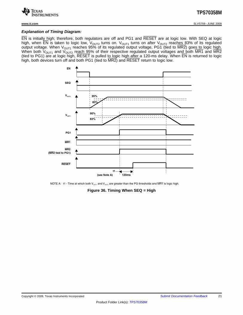
Explanation of Timing Diagram:EN is initially high; therefore, both regulators are off and PG1 and RESET are at logic low. With SEQ at logichigh, when EN is taken to logic low, VOUT2 turns on. VOUT1 turns on after VOUT2 reaches 83% of its regulatedoutput voltage. When VOUT1 reaches 95% of its regulated output voltage, PG1 (tied to MR2) goes to logic high.When both VOUT1 and VOUT2 reach 95% of their respective regulated output voltages and both MR1 and MR2(tied to PG1) are at logic high, RESET is pulled to logic high after a 120-ms delay. When EN is returned to logichigh, both devices turn off and both PG1 (tied to MR2) and RESET return to logic low.
Figure 36. Timing When SEQ = High
Copyright © 2009, Texas Instruments Incorporated Submit Documentation Feedback 21
Product Folder Link(s): TPS70358M
Toggled MR1
VOUT2
VIN1
VIN2
EN
SEQ
VOUT1
VSENSE1
PG1
MR2
RESET
MR1
VSENSE2
VOUT2
VIVOUT1
MR1
0.22 µ F
RESET
22 µ F
47 µ F
0.22 µ F
MR2
EN 2 V
0.7 V
TPS70358
(Fixed Output Option)
>2 V
<0.7 V
250 k Ω
TPS70358M
SLVS759–JUNE 2009 ...................................................................................................................................................................................................... www.ti.com
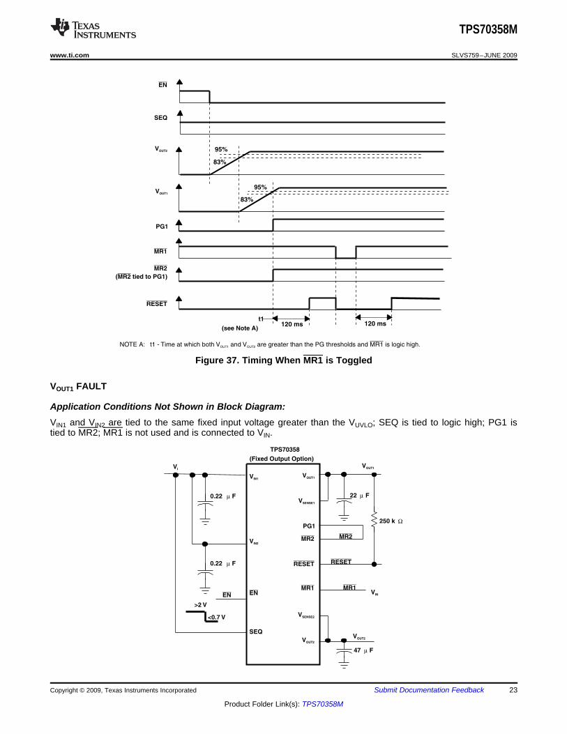
Application Conditions Not Shown in Block Diagram:VIN1 and VIN2 are tied to the same fixed input voltage greater than the VUVLO; SEQ is tied to logic high; PG1 istied to MR2; MR1 is initially at logic high but is eventually toggled.
Explanation of Timing Diagram:EN is initially high; therefore, both regulators are off and PG1 and RESET are at logic low. With SEQ at logichigh, when EN is taken low, VOUT2 turns on. VOUT1 turns on after VOUT2 reaches 83% of its regulated outputvoltage. When VOUT1 reaches 95% of its regulated output voltage, PG1 (tied to MR2) goes to logic high. Whenboth VOUT1 and VOUT2 reach 95% of their respective regulated output voltages and both MR1 and MR2 (tied toPG1) are at logic high, RESET is pulled to logic high after a 120-ms delay. When MR1 is taken low, RESETreturns to logic low but the outputs remain in regulation. When MR1 is returned to logic high, since both VOUT1and VOUT2 remain above 95% of their respective regulated output voltages and MR2 (tied to PG1) remains atlogic high, RESET is pulled to logic high after a 120-ms delay.
22 Submit Documentation Feedback Copyright © 2009, Texas Instruments Incorporated
Product Folder Link(s): TPS70358M
83%
95%
120 ms
EN
VOUT2
VOUT1
PG1
MR1
MR2
( tied to PG1)MR2
RESET
SEQ
120 ms
83%
95%
NOTE A: t1 - Time at which both V and V are greater than the PG thresholds and is logic high.OUT1 OUT2 MR1
t1
(see Note A)
VOUT1 FAULT
RESET
VOUT2
VIN1
VIN2
EN
SEQ
VOUT1
VSENSE1
PG1
MR2
RESET
MR1
VSENSE2
VOUT2
VIVOUT1
MR1
0.22 µ F 22 µ F
47 µ F
0.22 µ F
MR2
EN
TPS70358
(Fixed Output Option)
>2 V
<0.7 V
250 k Ω
VIN
TPS70358M
www.ti.com ...................................................................................................................................................................................................... SLVS759–JUNE 2009
Figure 37. Timing When MR1 is Toggled
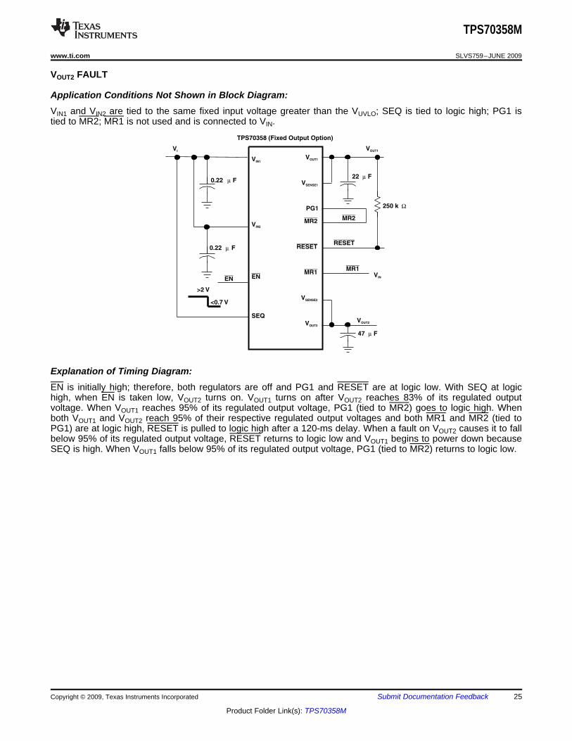
Application Conditions Not Shown in Block Diagram:VIN1 and VIN2 are tied to the same fixed input voltage greater than the VUVLO; SEQ is tied to logic high; PG1 istied to MR2; MR1 is not used and is connected to VIN.
Copyright © 2009, Texas Instruments Incorporated Submit Documentation Feedback 23
Product Folder Link(s): TPS70358M

120 ms
EN
VOUT2
VOUT1
PG1
MR1
MR2
( tied to PG1)MR2
RESET
SEQUENCE
95%
83%
83%
95%
NOTE A: t1 - Time at which both V and V are greater than the PG thresholds and is logic high.OUT1 OUT2 MR1
t1
(see Note A)
Fault on VOUT1
TPS70358M
SLVS759–JUNE 2009 ...................................................................................................................................................................................................... www.ti.com
Explanation of Timing Diagram:EN is initially high; therefore, both regulators are off and PG1 and RESET are at logic low. With SEQ at logichigh, when EN is taken low, VOUT2 turns on. VOUT1 turns on after VOUT2 reaches 83% of its regulated outputvoltage. When VOUT1 reaches 95% of its regulated output voltage, PG1 (tied to MR2) goes to logic high. Whenboth VOUT1 and VOUT2 reach 95% of their respective regulated output voltages and both MR1 and MR2 (tied toPG1) are at logic high, RESET is pulled to logic high after a 120-ms delay. When a fault on VOUT1 causes it to fallbelow 95% of its regulated output voltage, PG1 (tied to MR2) goes to logic low.
Figure 38. Timing When a Fault Occurs on VOUT1
24 Submit Documentation Feedback Copyright © 2009, Texas Instruments Incorporated
Product Folder Link(s): TPS70358M
VOUT2 FAULT
RESET
VOUT2
VIN1
VIN2
EN
SEQ
VOUT1
VSENSE1
PG1
MR2
RESET
MR1
VSENSE2
VOUT2
VI VOUT1
MR1
0.22 µ F22 µ F
47 µ F
0.22 µ F
MR2
EN
TPS70358 (Fixed Output Option)
>2 V
<0.7 V
250 k Ω
VIN
TPS70358M
www.ti.com ...................................................................................................................................................................................................... SLVS759–JUNE 2009
Application Conditions Not Shown in Block Diagram:VIN1 and VIN2 are tied to the same fixed input voltage greater than the VUVLO; SEQ is tied to logic high; PG1 istied to MR2; MR1 is not used and is connected to VIN.
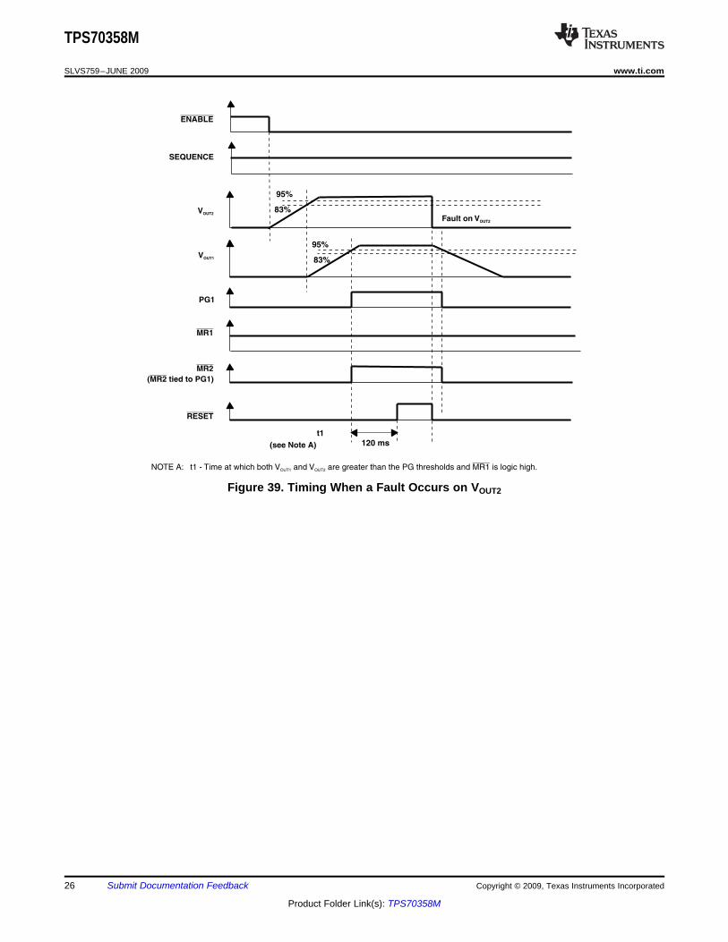
Explanation of Timing Diagram:EN is initially high; therefore, both regulators are off and PG1 and RESET are at logic low. With SEQ at logichigh, when EN is taken low, VOUT2 turns on. VOUT1 turns on after VOUT2 reaches 83% of its regulated outputvoltage. When VOUT1 reaches 95% of its regulated output voltage, PG1 (tied to MR2) goes to logic high. Whenboth VOUT1 and VOUT2 reach 95% of their respective regulated output voltages and both MR1 and MR2 (tied toPG1) are at logic high, RESET is pulled to logic high after a 120-ms delay. When a fault on VOUT2 causes it to fallbelow 95% of its regulated output voltage, RESET returns to logic low and VOUT1 begins to power down becauseSEQ is high. When VOUT1 falls below 95% of its regulated output voltage, PG1 (tied to MR2) returns to logic low.
Copyright © 2009, Texas Instruments Incorporated Submit Documentation Feedback 25
Product Folder Link(s): TPS70358M
83%
95%
83%
95%
120 ms
ENABLE
VOUT2
VOUT1
PG1
MR1
MR2
( tied to PG1)MR2
RESET
SEQUENCE
NOTE A: t1 - Time at which both V and V are greater than the PG thresholds and is logic high.OUT1 OUT2 MR1
t1
(see Note A)
Fault on VOUT2
TPS70358M
SLVS759–JUNE 2009 ...................................................................................................................................................................................................... www.ti.com
Figure 39. Timing When a Fault Occurs on VOUT2
26 Submit Documentation Feedback Copyright © 2009, Texas Instruments Incorporated
Product Folder Link(s): TPS70358M
Split Voltage DSP Application
2.5 V
VIN1
VIN2
EN
SEQ
VOUT1
VSENSE1
PG1
MR2
RESET
MR1
VSENSE2
VOUT2
TPS70358
5 V3.3 V
I/O
MR1
Core
0.22 µ F
RESET
22 µ F
47 µ F
0.22 µ F
DSP
MR2
PG1
EN
250 k Ω
>2 V
<0.7 V
250 k Ω
VIN
VIN
83%
95%
120ms
EN
VOUT2
(Core)
PG1
RESET
SEQ
95%
83%
VOUT1
(I/O)
NOTE A: t1 - Time at which both V and V are greater than the PG1 thresholds and is logic high.OUT1 OUT2 MR1
t1
(see Note A)
TPS70358M
www.ti.com ...................................................................................................................................................................................................... SLVS759–JUNE 2009
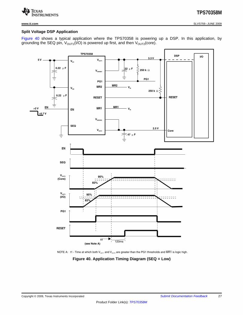
Figure 40 shows a typical application where the TPS70358 is powering up a DSP. In this application, bygrounding the SEQ pin, VOUT1(I/O) is powered up first, and then VOUT2(core).
Figure 40. Application Timing Diagram (SEQ = Low)
Copyright © 2009, Texas Instruments Incorporated Submit Documentation Feedback 27
Product Folder Link(s): TPS70358M
VIN1
VIN2
EN
SEQ
VOUT1
VSENSE1
PG1
MR2
RESET
MR1
VSENSE2
VOUT2
TPS70358
5 V
0.22
µ F0.22
2.5 V
3.3 VI/O
MR1
Core
RESET
22 µ F
47 µ F
DSP
MR2
PG1
250 k Ω
EN>2 V
<0.7 V
250 k Ω
VIN
VIN
µ F
83%
95%
83%
95%
120ms
EN
VOUT2
(Core)
VOUT1
(I/O)
PG1
RESET
SEQ
NOTE A: t1 - Time at which both V and V are greater than the PG1 thresholds and is logic high.OUT1 OUT2 MR1
t1
(see Note A)
Input Capacitor
TPS70358M
SLVS759–JUNE 2009 ...................................................................................................................................................................................................... www.ti.com
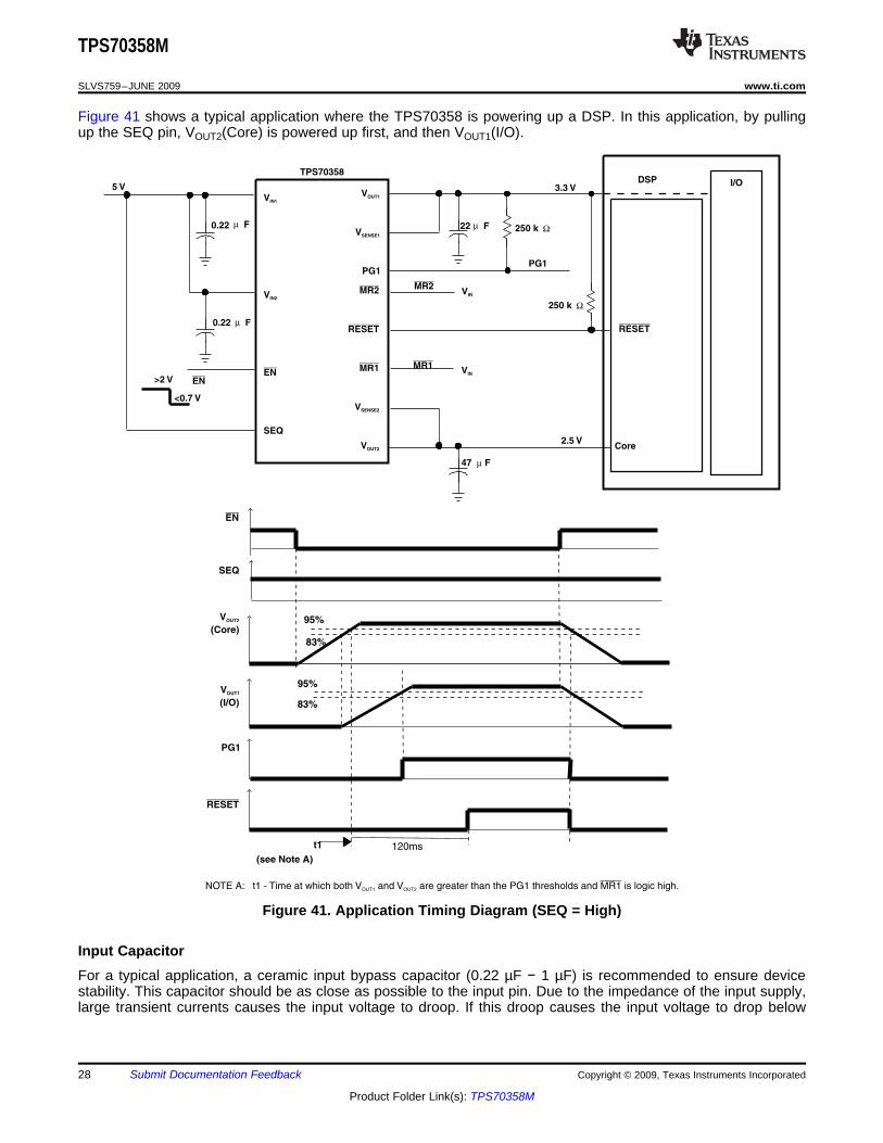
Figure 41 shows a typical application where the TPS70358 is powering up a DSP. In this application, by pullingup the SEQ pin, VOUT2(Core) is powered up first, and then VOUT1(I/O).
Figure 41. Application Timing Diagram (SEQ = High)
For a typical application, a ceramic input bypass capacitor (0.22 µF − 1 µF) is recommended to ensure devicestability. This capacitor should be as close as possible to the input pin. Due to the impedance of the input supply,large transient currents causes the input voltage to droop. If this droop causes the input voltage to drop below
28 Submit Documentation Feedback Copyright © 2009, Texas Instruments Incorporated
Product Folder Link(s): TPS70358M

Output Capacitor
Regulator Protection
TPS70358M
www.ti.com ...................................................................................................................................................................................................... SLVS759–JUNE 2009
the UVLO threshold, the device turns off. Therefore, it is recommended that a larger capacitor be placed inparallel with the ceramic bypass capacitor at the regulator’s input. The size of this capacitor depends on theoutput current, response time of the main power supply, and the main power supply’s distance to the regulator.At a minimum, the capacitor should be sized to ensure that the input voltage does not drop below the minimumUVLO threshold voltage during normal operating conditions.
As with most LDO regulators, the TPS70358 requires an output capacitor connected between each OUT andGND to stabilize the internal control loop. The minimum recommended capacitance value for VOUT1 is 22 µF andthe ESR (equivalent series resistance) must be between 50 mΩ and 800 mΩ. The minimum recommendedcapacitance value for VOUT2 is 47 µF and the ESR must be between 50 mΩ and 2 Ω. Solid tantalum electrolytic,aluminum electrolytic, and multilayer ceramic capacitors are all suitable, provided they meet the requirementsdescribed above. Larger capacitors provide a wider range of stability and better load transient response. Below isa partial listing of surface-mount capacitors usable with the TPS703xx for fast transient response application.
This information, along with the ESR graphs, is included to assist in selection of suitable capacitance for theuser’s application. When necessary to achieve low height requirements along with high output current and/orhigh load capacitance, several higher ESR capacitors can be used in parallel to meet the guidelines above.
VALUE MANUFACTURER PART NO.680 µF Kemet T510X6871004AS470 µF Sanyo 4TPB470M150 µF Sanyo 4TPC150M220 µF Sanyo 2R5TPC220M100 µF Sanyo 6TPC100M68 µF Sanyo 10TPC68M68 µF Kemet T495D6861006AS47 µF Kemet T495D4761010AS33 µF Kemet T495C3361016AS22 µF Kemet T495C2261010AS
Both TPS70358 PMOS-pass transistors have built-in back diodes that conduct reverse currents when the inputvoltage drops below the output voltage (e.g., during power down). Current is conducted from the output to theinput and is not internally limited. When extended reverse voltage is anticipated, external limiting may beappropriate.
The TPS70358 also features internal current limiting and thermal protection. During normal operation, theTPS70358 regulator 1 limits output current to approximately 1.75 A (typ) and regulator 2 limits output current toapproximately 3.8 A (typ). When current limiting engages, the output voltage scales back linearly until theovercurrent condition ends. While current limiting is designed to prevent gross device failure, care should betaken not to exceed the power dissipation ratings of the package. If the temperature of the device exceeds150°C(typ), thermal-protection circuitry shuts it down. Once the device has cooled below 130°C(typ), regulatoroperation resumes.
Copyright © 2009, Texas Instruments Incorporated Submit Documentation Feedback 29
Product Folder Link(s): TPS70358M

PACKAGING INFORMATION
Orderable Device Status (1) PackageType
PackageDrawing
Pins PackageQty
Eco Plan (2) Lead/Ball Finish MSL Peak Temp (3)
TPS70358MHKH ACTIVE CFP HKH 20 25 TBD Call TI N / A for Pkg Type
(1) The marketing status values are defined as follows:ACTIVE: Product device recommended for new designs.LIFEBUY: TI has announced that the device will be discontinued, and a lifetime-buy period is in effect.NRND: Not recommended for new designs. Device is in production to support existing customers, but TI does not recommend using this part ina new design.PREVIEW: Device has been announced but is not in production. Samples may or may not be available.OBSOLETE: TI has discontinued the production of the device.
(2) Eco Plan - The planned eco-friendly classification: Pb-Free (RoHS), Pb-Free (RoHS Exempt), or Green (RoHS & no Sb/Br) - please checkhttp://www.ti.com/productcontent for the latest availability information and additional product content details.TBD: The Pb-Free/Green conversion plan has not been defined.Pb-Free (RoHS): TI's terms "Lead-Free" or "Pb-Free" mean semiconductor products that are compatible with the current RoHS requirementsfor all 6 substances, including the requirement that lead not exceed 0.1% by weight in homogeneous materials. Where designed to be solderedat high temperatures, TI Pb-Free products are suitable for use in specified lead-free processes.Pb-Free (RoHS Exempt): This component has a RoHS exemption for either 1) lead-based flip-chip solder bumps used between the die andpackage, or 2) lead-based die adhesive used between the die and leadframe. The component is otherwise considered Pb-Free (RoHScompatible) as defined above.Green (RoHS & no Sb/Br): TI defines "Green" to mean Pb-Free (RoHS compatible), and free of Bromine (Br) and Antimony (Sb) based flameretardants (Br or Sb do not exceed 0.1% by weight in homogeneous material)
(3) MSL, Peak Temp. -- The Moisture Sensitivity Level rating according to the JEDEC industry standard classifications, and peak soldertemperature.
Important Information and Disclaimer:The information provided on this page represents TI's knowledge and belief as of the date that it isprovided. TI bases its knowledge and belief on information provided by third parties, and makes no representation or warranty as to theaccuracy of such information. Efforts are underway to better integrate information from third parties. TI has taken and continues to takereasonable steps to provide representative and accurate information but may not have conducted destructive testing or chemical analysis onincoming materials and chemicals. TI and TI suppliers consider certain information to be proprietary, and thus CAS numbers and other limitedinformation may not be available for release.
In no event shall TI's liability arising out of such information exceed the total purchase price of the TI part(s) at issue in this document sold by TIto Customer on an annual basis.
OTHER QUALIFIED VERSIONS OF TPS70358M :
• Catalog: TPS70358
NOTE: Qualified Version Definitions:
• Catalog - TI's standard catalog product
PACKAGE OPTION ADDENDUM
www.ti.com 15-Jul-2009
Addendum-Page 1

IMPORTANT NOTICETexas Instruments Incorporated and its subsidiaries (TI) reserve the right to make corrections, modifications, enhancements, improvements,and other changes to its products and services at any time and to discontinue any product or service without notice. Customers shouldobtain the latest relevant information before placing orders and should verify that such information is current and complete. All products aresold subject to TI’s terms and conditions of sale supplied at the time of order acknowledgment.TI warrants performance of its hardware products to the specifications applicable at the time of sale in accordance with TI’s standardwarranty. Testing and other quality control techniques are used to the extent TI deems necessary to support this warranty. Except wheremandated by government requirements, testing of all parameters of each product is not necessarily performed.TI assumes no liability for applications assistance or customer product design. Customers are responsible for their products andapplications using TI components. To minimize the risks associated with customer products and applications, customers should provideadequate design and operating safeguards.TI does not warrant or represent that any license, either express or implied, is granted under any TI patent right, copyright, mask work right,or other TI intellectual property right relating to any combination, machine, or process in which TI products or services are used. Informationpublished by TI regarding third-party products or services does not constitute a license from TI to use such products or services or awarranty or endorsement thereof. Use of such information may require a license from a third party under the patents or other intellectualproperty of the third party, or a license from TI under the patents or other intellectual property of TI.Reproduction of TI information in TI data books or data sheets is permissible only if reproduction is without alteration and is accompaniedby all associated warranties, conditions, limitations, and notices. Reproduction of this information with alteration is an unfair and deceptivebusiness practice. TI is not responsible or liable for such altered documentation. Information of third parties may be subject to additionalrestrictions.Resale of TI products or services with statements different from or beyond the parameters stated by TI for that product or service voids allexpress and any implied warranties for the associated TI product or service and is an unfair and deceptive business practice. TI is notresponsible or liable for any such statements.TI products are not authorized for use in safety-critical applications (such as life support) where a failure of the TI product would reasonablybe expected to cause severe personal injury or death, unless officers of the parties have executed an agreement specifically governingsuch use. Buyers represent that they have all necessary expertise in the safety and regulatory ramifications of their applications, andacknowledge and agree that they are solely responsible for all legal, regulatory and safety-related requirements concerning their productsand any use of TI products in such safety-critical applications, notwithstanding any applications-related information or support that may beprovided by TI. Further, Buyers must fully indemnify TI and its representatives against any damages arising out of the use of TI products insuch safety-critical applications.TI products are neither designed nor intended for use in military/aerospace applications or environments unless the TI products arespecifically designated by TI as military-grade or "enhanced plastic." Only products designated by TI as military-grade meet militaryspecifications. Buyers acknowledge and agree that any such use of TI products which TI has not designated as military-grade is solely atthe Buyer's risk, and that they are solely responsible for compliance with all legal and regulatory requirements in connection with such use.TI products are neither designed nor intended for use in automotive applications or environments unless the specific TI products aredesignated by TI as compliant with ISO/TS 16949 requirements. Buyers acknowledge and agree that, if they use any non-designatedproducts in automotive applications, TI will not be responsible for any failure to meet such requirements.Following are URLs where you can obtain information on other Texas Instruments products and application solutions:Products ApplicationsAmplifiers amplifier.ti.com Audio www.ti.com/audioData Converters dataconverter.ti.com Automotive www.ti.com/automotiveDLP® Products www.dlp.com Broadband www.ti.com/broadbandDSP dsp.ti.com Digital Control www.ti.com/digitalcontrolClocks and Timers www.ti.com/clocks Medical www.ti.com/medicalInterface interface.ti.com Military www.ti.com/militaryLogic logic.ti.com Optical Networking www.ti.com/opticalnetworkPower Mgmt power.ti.com Security www.ti.com/securityMicrocontrollers microcontroller.ti.com Telephony www.ti.com/telephonyRFID www.ti-rfid.com Video & Imaging www.ti.com/videoRF/IF and ZigBee® Solutions www.ti.com/lprf Wireless www.ti.com/wireless
Mailing Address: Texas Instruments, Post Office Box 655303, Dallas, Texas 75265Copyright © 2009, Texas Instruments Incorporated