dual-output, multimode cd-rw/dvd laser-diode drivers · pdf filegeneral description the...
TRANSCRIPT
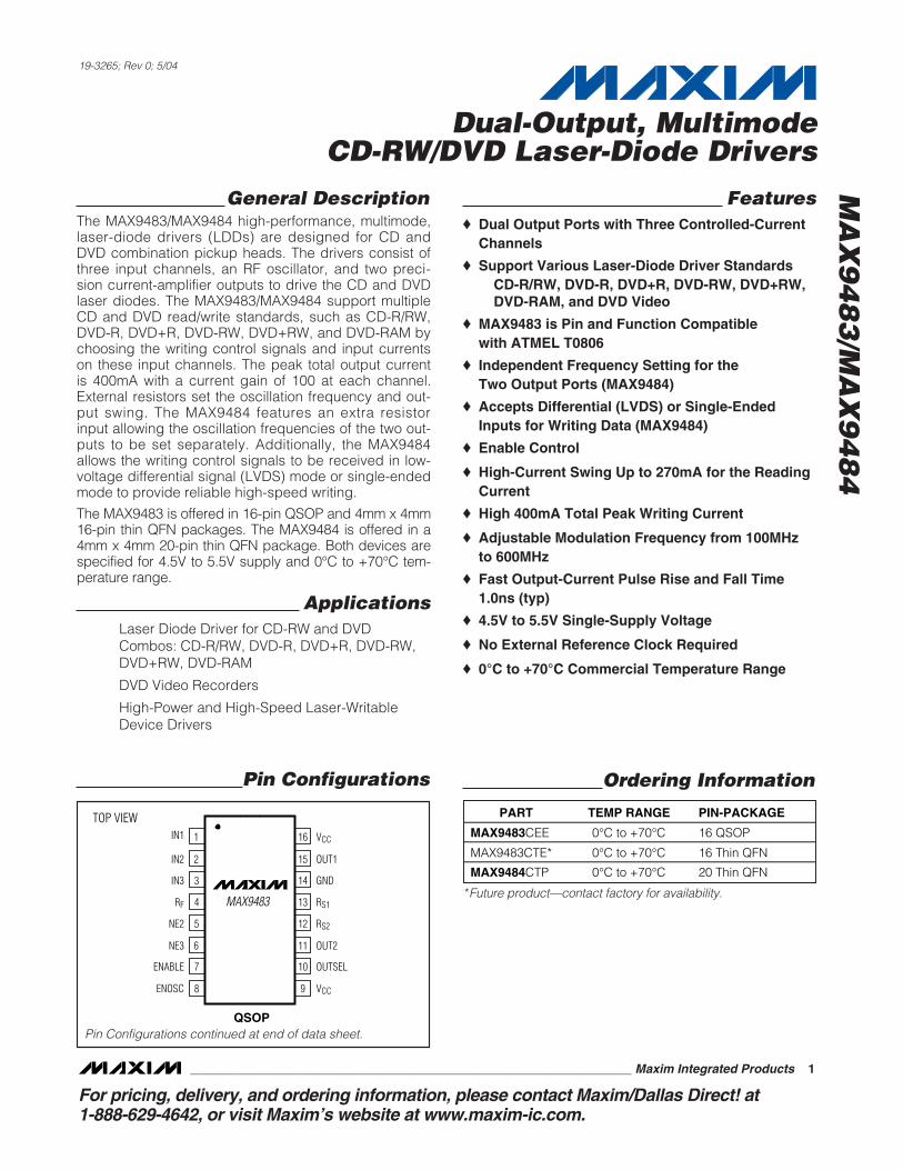
General DescriptionThe MAX9483/MAX9484 high-performance, multimode,laser-diode drivers (LDDs) are designed for CD andDVD combination pickup heads. The drivers consist ofthree input channels, an RF oscillator, and two preci-sion current-amplifier outputs to drive the CD and DVDlaser diodes. The MAX9483/MAX9484 support multipleCD and DVD read/write standards, such as CD-R/RW,DVD-R, DVD+R, DVD-RW, DVD+RW, and DVD-RAM bychoosing the writing control signals and input currentson these input channels. The peak total output currentis 400mA with a current gain of 100 at each channel.External resistors set the oscillation frequency and out-put swing. The MAX9484 features an extra resistorinput allowing the oscillation frequencies of the two out-puts to be set separately. Additionally, the MAX9484allows the writing control signals to be received in low-voltage differential signal (LVDS) mode or single-endedmode to provide reliable high-speed writing.
The MAX9483 is offered in 16-pin QSOP and 4mm x 4mm16-pin thin QFN packages. The MAX9484 is offered in a4mm x 4mm 20-pin thin QFN package. Both devices arespecified for 4.5V to 5.5V supply and 0°C to +70°C tem-perature range.
ApplicationsLaser Diode Driver for CD-RW and DVDCombos: CD-R/RW, DVD-R, DVD+R, DVD-RW,DVD+RW, DVD-RAM
DVD Video Recorders
High-Power and High-Speed Laser-WritableDevice Drivers
Features♦ Dual Output Ports with Three Controlled-Current
Channels
♦ Support Various Laser-Diode Driver StandardsCD-R/RW, DVD-R, DVD+R, DVD-RW, DVD+RW, DVD-RAM, and DVD Video
♦ MAX9483 is Pin and Function Compatible with ATMEL T0806
♦ Independent Frequency Setting for the Two Output Ports (MAX9484)
♦ Accepts Differential (LVDS) or Single-EndedInputs for Writing Data (MAX9484)
♦ Enable Control
♦ High-Current Swing Up to 270mA for the ReadingCurrent
♦ High 400mA Total Peak Writing Current
♦ Adjustable Modulation Frequency from 100MHz to 600MHz
♦ Fast Output-Current Pulse Rise and Fall Time1.0ns (typ)
♦ 4.5V to 5.5V Single-Supply Voltage
♦ No External Reference Clock Required
♦ 0°C to +70°C Commercial Temperature Range
MA
X9
48
3/M
AX
94
84
Dual-Output, MultimodeCD-RW/DVD Laser-Diode Drivers
________________________________________________________________ Maxim Integrated Products 1
16
15
14
13
12
11
10
9
1
2
3
4
5
6
7
8
IN1 VCC
OUT1
GND
RS1
RS2
OUT2
OUTSEL
VCC
TOP VIEW
MAX9483
QSOP
IN2
IN3
NE3
RF
NE2
ENABLE
ENOSC
Pin Configurations Ordering Information
19-3265; Rev 0; 5/04
For pricing, delivery, and ordering information, please contact Maxim/Dallas Direct! at 1-888-629-4642, or visit Maxim’s website at www.maxim-ic.com.
Pin Configurations continued at end of data sheet.
PART TEMP RANGE PIN-PACKAGE
MAX9483CEE 0°C to +70°C 16 QSOP
MAX9483CTE* 0°C to +70°C 16 Thin QFN
MAX9484CTP 0°C to +70°C 20 Thin QFN
*Future product—contact factory for availability.

MA
X9
48
3/M
AX
94
84
Dual-Output, MultimodeCD-RW/DVD Laser-Diode Drivers
2 _______________________________________________________________________________________
ABSOLUTE MAXIMUM RATINGS
DC ELECTRICAL CHARACTERISTICS(VCC = VCCO_ = +4.5V to +5.5V, RL = 6.8Ω, ENABLE = high, NE2 = NE3 = high (MAX9483), NE2_ = NE3_ = differential high(MAX9484), ENOSC = low, TA = 0°C to +70°C, unless otherwise noted. Typical values are at VCC = VCCO_ = +5V, TA = +25°C.)(Notes 1, 2, 4)
Stresses beyond those listed under “Absolute Maximum Ratings” may cause permanent damage to the device. These are stress ratings only, and functionaloperation of the device at these or any other conditions beyond those indicated in the operational sections of the specifications is not implied. Exposure toabsolute maximum rating conditions for extended periods may affect device reliability.
VCC, VCCO_ to GND ..............................................-0.3V to +6.0VIN_, RF_, RS_ to GND..................................-0.3V to (VCC + 0.3V)ENABLE, ENOSC, NE2_, NE3_,
OUTSEL to GND.....................................-0.3V to (VCC + 0.3V)Output Voltage at OUT1, OUT2......................-0.3V to (VCC - 1V)Continuous Power Dissipation (TA = +70°C)
QSOP (derate 8.3mW/°C above +70°C)........................667mWTQFN (derate 16.9mW/°C above +70°C).....................1349mW
Junction Temperature ......................................................+150°CStorage Temperature Range .............................-65°C to +150°CESD Rating (Human Body Model) .................................≥ ±2.0kVLead Temperature (soldering, 10s) .................................+300°C
PARAMETER SYMBOL CONDITIONS MIN TYP MAX UNITS
POWER SUPPLY
MAX9483 181 200Write-Mode Supply Current ICC1
IIN1 = IIN2 = IIN3 = 500µA,NE2 = NE3 = low MAX9484 182 210
mA
MAX9483 91 100Oscillator enabled,IIN1 = IIN2 = IIN3 = 500µA,ENOSC = high, RS = 8.2kΩ,RF = 6.8kΩ MAX9484 92 105
MAX9483 82 95
Read-Mode Supply Current ICC2
Oscillator disabled,IIN1 = IIN2 = IIN3 = 500µA MAX9484 83 95
mA
MAX9483 14 20Supply Current ICC3
Input disabled,IIN1 = IIN2 = IIN3 = 0 MAX9484 14 20
mA
MAX9483 0.96 2.0Power-Down Supply Current ICC4
ENABLE = NE2 = NE3 = low,IIN1 = IIN2 = IIN3 = 0 MAX9484 1.2 2.0
mA
DIGITAL INPUTS FOR WRITE CHANNEL CONTROL (NE2, NE3) (MAX9483)
High-Level Input Voltage VIH1 2.0 V
Low-Level Input Voltage VIL1 0.8 V
Input Current IIN1 VIN = high or low -20 +20 µA
LVDS DIGITAL INPUTS FOR WRITE CHANNEL CONTROL (NE2_, NE3_) (MAX9484)
Differential Input High Threshold VTH 50 mV
Differential Input Low Threshold VTL -50 mV
SINGLE-ENDED DIGITAL INPUTS FOR WRITE CHANNEL CONTROL (NE2+, NE3+) (MAX9484)
Reference Voltage VREF 1.10 1.25 1.40 V
High-Level Input Voltage VIH2VREF +
300mV
Low-Level Input Voltage VIL2VREF -300
mV
Input Current IIN2 VIN = high or low -20 +20 µA
MA
X9
48
3/M
AX
94
84
Dual-Output, MultimodeCD-RW/DVD Laser-Diode Drivers
_______________________________________________________________________________________ 3
DC ELECTRICAL CHARACTERISTICS (continued)(VCC = VCCO_ = +4.5V to +5.5V, RL = 6.8Ω, ENABLE = high, NE2 = NE3 = high (MAX9483), NE2_ = NE3_ = differential high(MAX9484), ENOSC = low, TA = 0°C to +70°C, unless otherwise noted. Typical values are at VCC = VCCO_ = +5V, TA = +25°C.)(Notes 1, 2, 4)
PARAMETER SYMBOL CONDITIONS MIN TYP MAX UNITS
DIGITAL INPUTS FOR CONTROL SIGNALS (ENABLE, OUTSEL, ENOSC)
High-Level Input Voltage VIH3 2.0 V
Low-Level Input Voltage VIL3 0.8 V
Input Current IIN3 VIN = high or low -10 +10 µA
ANALOG INPUTS (IN1, IN2, IN3)
Current Channel Input CurrentRange
ICIN Current flowing into IN1, IN2, or IN3 0 4.0 mA
Current Channel InputImpedance
RIN IN_ to GND 165 200 235 Ω
OUTPUTS (OUT1 and OUT2)
Maximum Total Output Current IOUT 320 400 mA
Read current IN1 210 273Maximum Output Current perChannel
IOUTWrite current IN2, IN3 250 347
mA
Best-Fit Current Gain AI Any channel (Note 3) 100 I/I
Best-Fit Current Offset IOFFSET Any channel (Note 3) -4 +4 mA
Output Current Linearity Any channel (Note 3) -3 +3 %
IOFF1 ENABLE = low 0.2 1
IOFF2NE2 = NE3 = high, IIN1 = 0µA,IIN2 = IIN3 = 500µA
0.22 1.5Output Off Current
IOFF3 NE2 = NE3 = low, IIN1 = IIN2 = IIN3 = 0µA 0.14 5
mA
Read-Mode Output SupplySensitivity
IOUT = 40mA -2 +2 %/V
Write-Mode Output SupplySensitivity
IOUT = 80mA -2 +2 %/V
Read-Mode Output TemperatureSensitivity
IOUT = 40mA 15 ppm°C
Write-Mode Output TemperatureSensitivity
IOUT = 80mA 16 ppm°C
Output Noise IOUT = 40mA, ENOSC = low 3 nA/√Hz
MA
X9
48
3/M
AX
94
84
Dual-Output, MultimodeCD-RW/DVD Laser-Diode Drivers
4 _______________________________________________________________________________________
Note 1: Current into a pin is defined as positive. Current out of a pin is defined as negative. All voltages are referenced to groundexcept VTH.
Note 2: Maximum and minimum limits over temperature are guaranteed by design and characterization. Devices are productiontested at TA = +25°C.
Note 3: Linearity of the amplifier is calculated using a best-fit method at three operating points of IOUT at 20mA, 40mA, and 60mA.IOUT = (IIN x GAIN) + IOFFSET.
Note 4: Guaranteed by design and characterization. Limit set at ±6 sigma.
AC ELECTRICAL CHARACTERISTICS(VCC = VCCO_ = +4.5V to +5.5V, IOUT = 40mA (read) + 40mA, RL = 6.8Ω, ENABLE = high, NE2 = NE3 = high (MAX9483), NE2_ =NE3_ = differential high (MAX9484), ENOSC = low, TA = 0°C to +70°C, unless otherwise noted. Typical values are at VCC = VCCO_ =+5V, TA = +25°C.) (Notes 1, 4)
PARAMETER SYMBOL CONDITIONS MIN TYP MAX UNITS
OSCILLATOR
Oscillator Frequency fOSC RF_ = 7.5kΩ (Note 2), IOUT = 40mA (read) 255 300 350 MHz
Oscillator TemperatureCoefficient
RF_ = 7.5kΩ 10 ppm/°C
OUTPUT TIMING
Write Rise Time tr IOUT = 40mA (read) + 40mA (10% to 90%) 0.9 1.6 ns
Write Fall Time tf IOUT = 40mA (read) + 40mA (90% to 10%) 1.0 1.6 ns
Output-Current Overshoot OCO 5 %
Output ON Propagation Delay tON NE 50% high-low to IOUT at 50% of final value 1.0 2.0 ns
Output OFF Propagation Delay tOFF NE 50% low-high to IOUT at 50% of final value 1.0 2.0 ns
Output Disable Time tDISENABLE 50% high-low to IOUT at 50% of finalvalue at IOUT = 40mA (read)
60 100 ns
Output Enable Time tENENABLE 50% low-high to IOUT at 50% of finalvalue at IOUT = 40mA (read)
60 100 ns
Oscillator Disable Time tDISOENOSC 50% high-low to IOUT at 50% of finalvalue at IOUT = 40mA (read)
4 10 ns
Oscillator Enable Time tEHOENOSC 50% high-low to IOUT at 50% of finalvalue at IOUT = 40mA (read)
25 50 ns
tODHOUTSEL 50% low-high to IOUT at 50% of finalvalue measured at OUT1
2.9 10
Channel-Select Delay
tODLOUTSEL 50% high-low to IOUT at 50% of finalvalue measured at OUT2
2.9 10
ns

MA
X9
48
3/M
AX
94
84
Dual-Output, MultimodeCD-RW/DVD Laser-Diode Drivers
_______________________________________________________________________________________ 5
100
200
300
400
500
600
700
3 54 6 7 8 9 10 11 12
OSCILLATOR FREQUENCYvs. RESISTOR RF
MAX
9483
toc0
1
RF (kΩ)
FREQ
UENC
Y (M
Hz)
0
20
10
40
30
70
60
50
80
3 54 6 7 8 9 10
OSCILLATOR PEAK-TO-PEAK SWINGvs. RESISTOR RS
MAX
9483
toc0
2
RS (kΩ)
SWIN
G (m
A P-P
)
0
20
10
40
30
60
50
70
90
80
100
200 300 350250 400 450 500 550 600
OSCILLATOR PEAK-TO-PEAK SWINGvs. FREQUENCY
MAX
9483
toc0
3
FREQUENCY (MHz)
SWIN
G (m
A P-P
)
280
290
285
300
295
315
310
305
320
0 2010 30 40 50 60 70
OSCILLATOR FREQUENCYvs. TEMPERATURE
MAX
9483
toc0
4
TEMPERATURE (°C)
FREQ
UENC
Y (M
Hz)
0
100
50
250
200
150
400
350
300
450
0 600300 900 1200 1500
OUTPUT CHANNEL CURRENTvs. INPUT CURRENT (IIN1 = IIN2 = IIN3)
MAX
9483
toc0
5
IIN_ (µA)
I OUT
(mA)
VCC = 5.25VVCC = 5.0V
VCC = 4.75V
0
100
50
200
150
300
250
350
0 21 3 4 5
OUTPUT VOLTAGE COMPLIANCE
MAX
9483
toc0
6
VCC - VOUT (V)
I OUT
(mA)
50mA +50mA PULSE (10ns)MAX9483 toc07
TIME (5ns/div)
Typical Operating Characteristics(VCC = VCCO_ = +5V, TA = +25°C, unless otherwise noted.)
MA
X9
48
3/M
AX
94
84
Dual-Output, MultimodeCD-RW/DVD Laser-Diode Drivers
6 _______________________________________________________________________________________
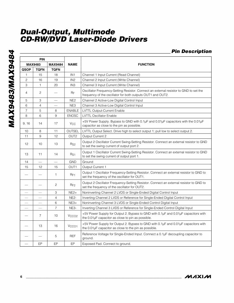
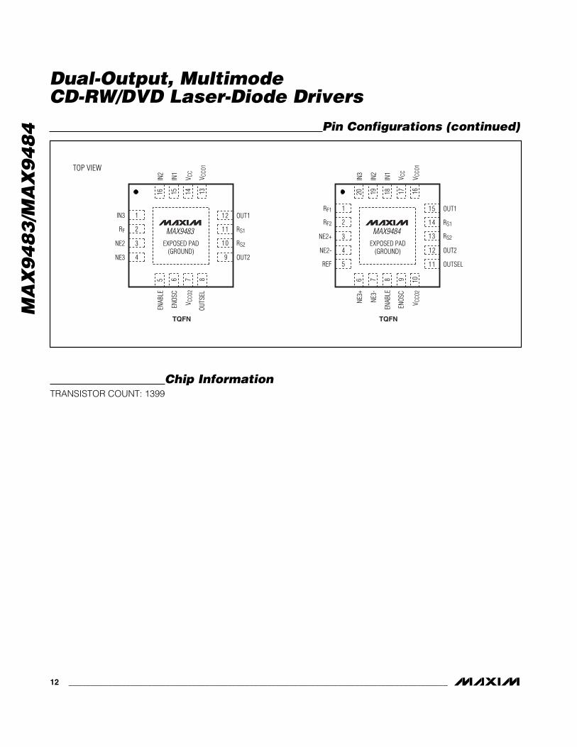
Pin DescriptionPIN
MAX9483 MAX9484
QSOP TQFN TQFN
NAME FUNCTION
1 15 18 IN1 Channel 1 Input Current (Read Channel)
2 16 19 IN2 Channel 2 Input Current (Write Channel)
3 1 20 IN3 Channel 3 Input Current (Write Channel)
4 2 — RFOscillator Frequency-Setting Resistor. Connect an external resistor to GND to set thefrequency of the oscillator for both outputs OUT1 and OUT2.
5 3 — NE2 Channel 2 Active-Low Digital Control Input
6 4 — NE3 Channel 3 Active-Low Digital Control Input
7 5 8 ENABLE LVTTL Output-Current Enable
8 6 9 ENOSC LVTTL Oscillator Enable
9, 16 14 17 VCC+5V Power Supply. Bypass to GND with 0.1µF and 0.01µF capacitors with the 0.01µFcapacitor as close to the pin as possible.
10 8 11 OUTSEL LVTTL Output Select. Drive high to select output 1; pull low to select output 2.
11 9 12 OUT2 Output Current 2
12 10 13 RS2Output 2 Oscillator Current Swing-Setting Resistor. Connect an external resistor to GNDto set the swing current of output port 2.
13 11 14 RS1Output 1 Oscillator Current Swing-Setting Resistor. Connect an external resistor to GNDto set the swing current of output port 1.
14 — — GND Ground
15 12 15 OUT1 Output Current 1
— — 1 RF1Output 1 Oscillator Frequency-Setting Resistor. Connect an external resistor to GND toset the frequency of the oscillator for OUT1.
— — 2 RF2Output 2 Oscillator Frequency-Setting Resistor. Connect an external resistor to GND toset the frequency of the oscillator for OUT2.
— — 3 NE2+ Noninverting Channel 2 LVDS or Single-Ended Digital Control Input
— — 4 NE2- Inverting Channel 2 LVDS or Reference for Single-Ended Digital Control Input
— — 6 NE3+ Noninverting Channel 3 LVDS or Single-Ended Control Digital Input
— — 7 NE3- Inverting Channel 3 LVDS or Reference for Single-Ended Control Digital Input
— 7 10 VCCO2+5V Power Supply for Output 2. Bypass to GND with 0.1µF and 0.01µF capacitors withthe 0.01µF capacitor as close to pin as possible.
— 13 16 VCCO1+5V Power Supply for Output 2. Bypass to GND with 0.1µF and 0.01µF capacitors withthe 0.01µF capacitor as close to the pin as possible.
— — 5 REFReference Voltage for Single-Ended Input. Connect a 0.1µF decoupling capacitor toground.
— EP EP EP Exposed Pad. Connect to ground.

MA
X9
48
3/M
AX
94
84
Dual-Output, MultimodeCD-RW/DVD Laser-Diode Drivers
_______________________________________________________________________________________ 7
ENABLE
NE2
NE3
tEN
tON
tON tOFF
tOFF
tDIS
tr
tr tf
tf
IOUT
H
L
H
L
H
L
TIME
Figure 1. Timing Diagram of Output vs. Control Signals
Detailed DescriptionRead Channel and Write Channels
The MAX9483/MAX9484 high-performance multimodeLDDs are designed for CD and DVD combination pick-up heads. The drivers have three current channels.Each channel has a current input IN_ (_ = 1, 2, or 3)and a channel control signal (ENABLE, NE2, or NE3).IN1 supplies the reference for the read channel, whichprovides the read current or the offset current to thelasers. The other two channels are the write channels.The currents of these two channels are superimposedon the read current that serves as the offset current forthe laser in write mode. The offset current significantlyreduces the laser output ramp-up time. When ENABLEis low, all three channels are disabled. Driving ENABLEhigh enables the read channel and leaves the other twowrite channels to be controlled by NE2 and NE3 (seeFigure 1). By selecting the input currents at IN2 and
IN3, as well as the signal timing of NE2 and NE3, thedrivers can generate various current waveforms for dif-ferent CD/DVD writing standards. All three channelshave a current gain of 100. The maximum total currenteach output can provide is 400mA.
RF OscillatorTo reduce the laser-mode hopping noise in read mode,modulate the read current with an oscillator with a100MHz to 600MHz frequency. An external resistor, RF,determines the oscillator frequency selection. For theMAX9484, two external resistors, RF1 and RF2, areused to select the oscillator frequency for CD and DVDlasers separately. The swing amplitude of the oscillatorcurrent is set by two external resistors, RS1 and RS2,one for CD and one for DVD. The oscillator is enabledwhen both ENABLE and ENOSC are driven high.

Applications InformationLVDS Inputs for MAX9484
The MAX9484 input control signals, NE2_ and NE3_, arecompatible with LVDS or single-ended inputs. The LVDSinputs allow the driver to handle higher data writingrates. When using single-ended input signals, such asLVTTL or SSTL_2, connect NE2- and NE3- to REF.
Laser Safety and IEC 825Using the MAX9483/MAX9484 laser drivers alone doesnot ensure that a transmitter design is compliant with IEC825. The entire transmitter circuit and component selec-tions must be considered. Customers must determinethe level of fault tolerance required by their application.Note that Maxim products are not designed or autho-rized for use as components in systems intended for sur-gical implantation into the body, for applicationsintended to support or sustain life, or for any other appli-cation where the failure of a Maxim product could createa situation where personal injury or death may occur.
MA
X9
48
3/M
AX
94
84
Dual-Output, MultimodeCD-RW/DVD Laser-Diode Drivers
8 _______________________________________________________________________________________
ENABLE
RF OSCILLATOR
RF RS1 RS2 OUTSEL
IN3
NE3
IN2
NE2
IN1
ENABLE
ENOSC
OUT1
OUT2
CONTROLCHANNEL 3
CONTROLCHANNEL 2
READCHANNEL
MAX9483
ENABLE
ENABLE
Figure 2. MAX9483 Functional Diagram
ENABLE
RF OSCILLATOR
VOLTAGEREFERENCE
RF1 RF2 RS2 OUTSEL
IN3
IN2
NE2+
IN1
ENABLE
ENOSC
REF
OUT1
OUT2
CONTROLCHANNEL 3
CONTROLCHANNEL 2
READCHANNEL
MAX9484
ENABLE
ENABLE
RS1
NE2-
NE3+
NE3-
Figure 3. MAX9484 Functional Diagram

MA
X9
48
3/M
AX
94
84
Dual-Output, MultimodeCD-RW/DVD Laser-Diode Drivers
_______________________________________________________________________________________ 9
IN3
IN2
IN1
V CC
V CC
OUT1
RF
OUT2
RS1RS1
RS2
RS2 RF
SINGLE-ENDED
INPUTS
+5V
LD1NE2
NE3EN
ABLE
ENOS
C OUTSEL
CONTROLSIGNALS
ANDCURRENT
INPUTS
LD2
OUTPUTSUPPLY
+5V CORE LOGICSUPPLY
MAX9483
Figure 4. MAX9483 Typical Operating Circuit

MA
X9
48
3/M
AX
94
84
Dual-Output, MultimodeCD-RW/DVD Laser-Diode Drivers
10 ______________________________________________________________________________________
IN3
IN2
IN1
V CC
V CCO
1
OUT1
RS1
RS2
OUT2
RF1RF1
RF1
RF2
LVDSINPUTS
+5V
LD1NE2+
NE2-
REF
NE3+
NE3-
ENAB
LE
ENOS
C
V CCO
2
+5VOUTPUT2SUPPLY
OUTSEL
CONTROLSIGNALS
ANDCURRENT
INPUTSLD2
OUTPUT1SUPPLY
+5V CORE LOGICSUPPLY
100Ω
100Ω
MAX9484
RS1
RS2
Figure 5. MAX9484 Typical Operating Circuit with LVDS Inputs

MA
X9
48
3/M
AX
94
84
Dual-Output, MultimodeCD-RW/DVD Laser-Diode Drivers
______________________________________________________________________________________ 11
IN3
IN2
IN1
V CC
V CCO
1
OUT1
RS1
RS2
OUT2
RF1RF1
RF2
RF2 RS1
RS2
SINGLE-ENDED
INPUTS
+5V
LD1NE2+
NE2-
REF
NE3+
NE3-
ENAB
LE
ENOS
C
V CCO
2
+5VOUTPUT2SUPPLY
OUTSEL
CONTROLSIGNALS
ANDCURRENT
INPUTS LD2
OUTPUT1SUPPLY
+5V CORE LOGICSUPPLY
MAX9484
Figure 6. MAX9484 Typical Operation Circuit with Single-Ended Inputs
MA
X9
48
3/M
AX
94
84
Dual-Output, MultimodeCD-RW/DVD Laser-Diode Drivers
12 ______________________________________________________________________________________
16 15 14 13
9
10
11
12
OUT2
RS2
RS1
OUT1
4
3
2
1
NE3
NE2
RF
IN3
MAX9483EXPOSED PAD
(GROUND)
MAX9484EXPOSED PAD
(GROUND)
IN2
IN1
V CC
V CCO
1
ENAB
LE
ENOS
C
V CCO
2
OUTS
EL
5 6 7 8
TQFN
20 19 18 17
12
13
14
15
OUT2
RS2
RS1
OUT1
4
3
2
1
NE2-
NE2+
RF2
RF1
11 OUTSEL5REF
IN3
IN2
IN1
V CC
NE3+
NE3-
ENAB
LE
ENOS
C
16
6 7 8 9 10V C
CO1
V CCO
2
TQFN
TOP VIEW
Pin Configurations (continued)
Chip InformationTRANSISTOR COUNT: 1399

MA
X9
48
3/M
AX
94
84
Dual-Output, MultimodeCD-RW/DVD Laser-Diode Drivers
______________________________________________________________________________________ 13
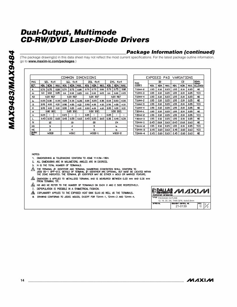
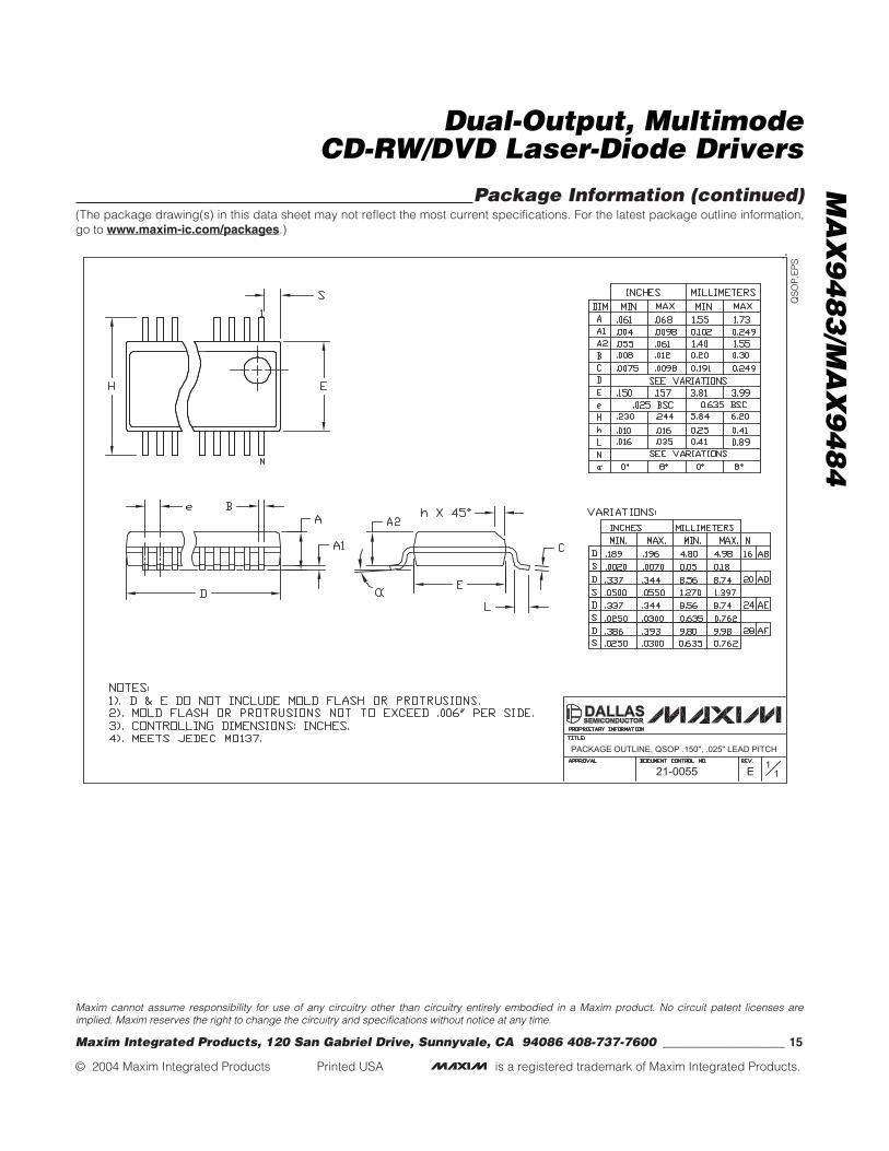
Package Information(The package drawing(s) in this data sheet may not reflect the most current specifications. For the latest package outline information,go to www.maxim-ic.com/packages.)
24L
QFN
TH
IN.E
PS
C1
221-0139
PACKAGE OUTLINE12, 16, 20, 24L THIN QFN, 4x4x0.8mm
MA
X9
48
3/M
AX
94
84
Dual-Output, MultimodeCD-RW/DVD Laser-Diode Drivers
14 ______________________________________________________________________________________
C2
221-0139
PACKAGE OUTLINE12, 16, 20, 24L THIN QFN, 4x4x0.8mm
Package Information (continued)(The package drawing(s) in this data sheet may not reflect the most current specifications. For the latest package outline information,go to www.maxim-ic.com/packages.)
MA
X9
48
3/M
AX
94
84
Dual-Output, MultimodeCD-RW/DVD Laser-Diode Drivers
Maxim cannot assume responsibility for use of any circuitry other than circuitry entirely embodied in a Maxim product. No circuit patent licenses areimplied. Maxim reserves the right to change the circuitry and specifications without notice at any time.
Maxim Integrated Products, 120 San Gabriel Drive, Sunnyvale, CA 94086 408-737-7600 ____________________ 15
© 2004 Maxim Integrated Products Printed USA is a registered trademark of Maxim Integrated Products.
Package Information (continued)(The package drawing(s) in this data sheet may not reflect the most current specifications. For the latest package outline information,go to www.maxim-ic.com/packages.)
QS
OP
.EP
S
E1
121-0055
PACKAGE OUTLINE, QSOP .150", .025" LEAD PITCH