dyesensitized tio2 nanotube solar cells: rational structural and surface engineering...
TRANSCRIPT
DOI: 10.1002/asia.201200349
Dye-Sensitized TiO2 Nanotube Solar Cells: Rational Structural and SurfaceEngineering on TiO2 Nanotubes
Jun Wang[a] and Zhiqun Lin*[b]
2754 � 2012 Wiley-VCH Verlag GmbH & Co. KGaA, Weinheim Chem. Asian J. 2012, 7, 2754 – 2762
FOCUS REVIEW

Abstract: Owing to well-defined structural parametersand enhanced electronic properties, highly ordered TiO2
nanotube arrays have been employed to substitute TiO2
nanoparticles for use in dye-sensitized solar cells. To fur-ther improve the performance of dye-sensitized TiO2
nanotube solar cells, efforts have been directed towardthe optimization of TiO2 photoanodes, dyes, electrolytes,and counter electrodes. Herein, we highlight recent prog-
ress in rational structural and surface engineering onanodic TiO2 nanotube arrays and their effects on improv-ing the power conversion efficiency of dye-sensitized TiO2
nanotube solar cells.
Keywords: dye-sensitized solar cells · electrochemistry ·nanostructures · surface chemistry · titanium
1. Introduction
Dye-sensitized solar cells (DSSCs) composed of nanostruc-tured photoanodes (e.g., TiO2 nanoparticle (NP) films),dyes, redox electrolytes, and counter electrodes have re-ceived considerable interest in the past two decades owingprimarily to their high solar-to-electricity conversion effi-ciency at a very competitive fabrication cost.[1] They presentan attractive alternative to conventional silicon-based solarcells. Tremendous efforts have been concentrated on im-proving device performance and stability by optimizing eachcomponent in the DSSCs and the design of device configu-ration to realize their significant commercial potentials.[2] Inrecent years, highly ordered TiO2 nanotube (NT) arrays, fab-ricated by electrochemical anodization of titanium in fluo-rine-containing electrolytes,[3] have been utilized as photoan-odes for DSSCs and shown improved charge-collection effi-ciency and enhanced light scattering compared with com-monly used TiO2 NP films (TPs).[1a,2b, 3e, 4] Vertically orientedTiO2 NT arrays (TNAs) with well-defined structural parame-ters, including pore size, tube length, wall thickness, and sur-face tomography, can be obtained by tuning the conditionsof electrochemical anodization.[3e, 4j] In comparison to elec-tron hopping between TiO2 NPs in conventional TiO2 photo-anodes, vertically aligned TiO2 NTs provide a vectorialcharge-transport pathway along the long axis of the NTs,thereby imparting longer electron lifetimes and reducedcharge recombination (Scheme 1).[2b, 4c,5] However, the over-all power conversion efficiency of dye-sensitized TiO2 NTsolar cells remained relatively low as a result of incompletecoverage of dye molecules on the TiO2 NT surface and in-sufficient infiltration of electrolyte into NTs. Clearly, the op-timization of structural parameters and surface properties ofTNAs is of key importance to achieve larger surface areasfor increased dye loading, better electronic interaction be-
tween dye and TiO2 surface, and more efficient charge trans-port.
Herein, we aim to highlight recent progress in improvingthe performance of dye-sensitized TiO2 NT solar cellsthrough rational structural and surface engineering on TiO2
NTs. First, we discuss the effects of structural modificationon TNAs on the performance of the resulting solar cells, in-cluding the integration of TiO2 NPs with TNAs, the forma-tion of hierarchically structured TiO2 NTs, the constructionof 3D NT arrays on Ti wire and mesh, and new designs ofdye-sensitized double-sided NT arrays. Subsequently, weassess the influence of surface engineering (i.e., TiCl4 treat-ment, oxygen plasma activation, and the doping of TNAswith a secondary species) on the photovoltaic performanceof dye-sensitized TiO2 NT solar cells.
2. Structural Engineering on TNAs
2.1. Integration of TiO2 NPs with TiO2 NTs
Integrating a TP with highly ordered TNAs has yielded twotypical configurations of photoanode in DSSCs: a TP–TNAbilayer[6] and TNAs filled with TiO2 NPs.[7]
Zheng et al. constructed a layer-by-layer hierarchical pho-toanode consisting of a TP and free-standing TNAs forDSSCs (Figure 1), which exhibited increased light-harvestingefficiency, longer electron lifetimes, and more efficient elec-tron extraction than those in single NP-film- or NT-array-based devices.[6a] Notably, TiO2 NPs used in this work wereprepared by breaking crystallized TNAs with high intensityultrasonication because crystalline TiO2 NTs were composedof small TiO2 nanocrystals and could be deformed by strongmechanical force.[8] With the optimum thickness of the TP(8 mm) and TNAs (9 mm) in the FTO-TP-TNA (FTO= fluo-rine-doped tin oxide) configuration, an overall power con-
[a] Dr. J. WangDepartment of Materials Science and EngineeringIowa State University, Ames, IA 50011 (USA)
[b] Prof. Z. LinSchool of Materials Science and EngineeringGeorgia Institute of Technology771 Ferst Dr., NW, Atlanta, GA 30332 (USA)E-mail : [email protected]: http://nanofm.mse.gatech.edu/
Scheme 1. Schematic illustration of electron transport in a) TPs andb) vertically aligned TiO2 NTs.
Chem. Asian J. 2012, 7, 2754 – 2762 � 2012 Wiley-VCH Verlag GmbH & Co. KGaA, Weinheim www.chemasianj.org 2755
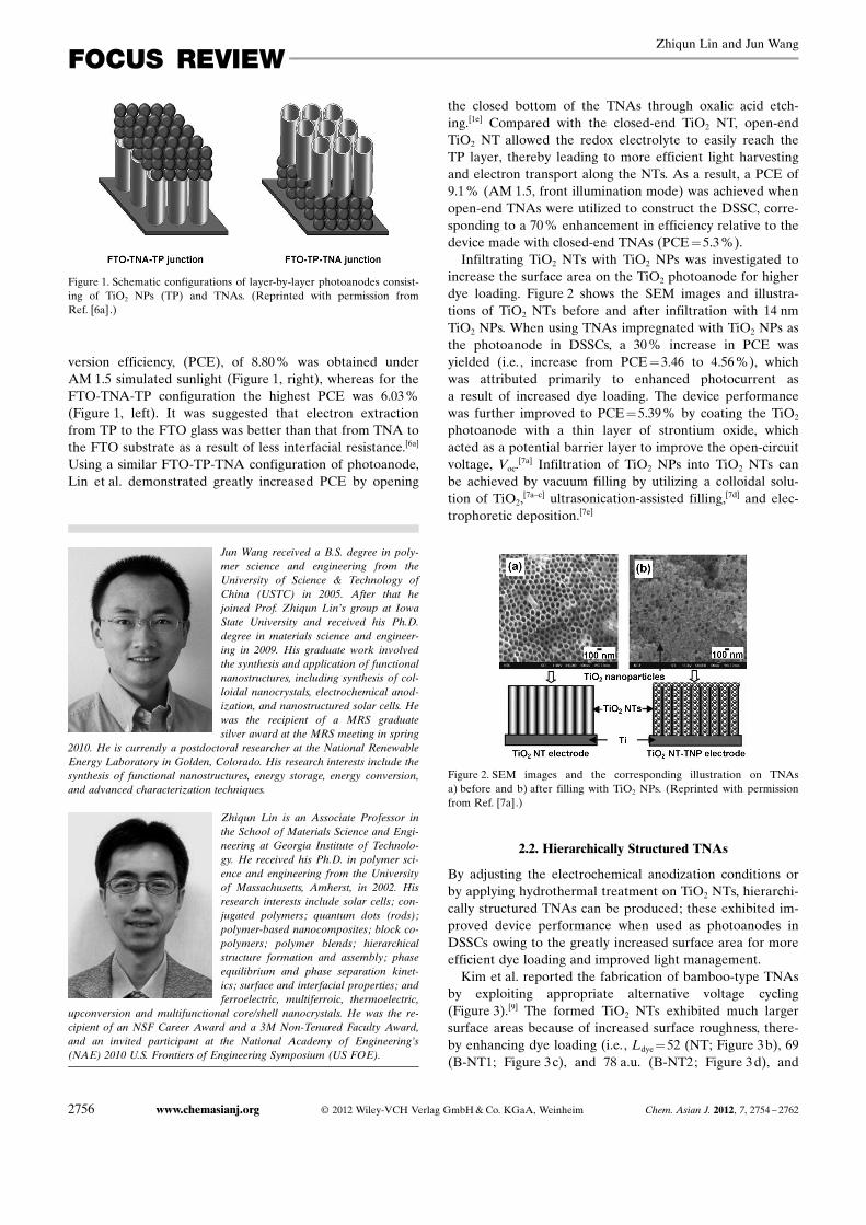
version efficiency, (PCE), of 8.80 % was obtained underAM 1.5 simulated sunlight (Figure 1, right), whereas for theFTO-TNA-TP configuration the highest PCE was 6.03 %(Figure 1, left). It was suggested that electron extractionfrom TP to the FTO glass was better than that from TNA tothe FTO substrate as a result of less interfacial resistance.[6a]
Using a similar FTO-TP-TNA configuration of photoanode,Lin et al. demonstrated greatly increased PCE by opening
the closed bottom of the TNAs through oxalic acid etch-ing.[1e] Compared with the closed-end TiO2 NT, open-endTiO2 NT allowed the redox electrolyte to easily reach theTP layer, thereby leading to more efficient light harvestingand electron transport along the NTs. As a result, a PCE of9.1 % (AM 1.5, front illumination mode) was achieved whenopen-end TNAs were utilized to construct the DSSC, corre-sponding to a 70 % enhancement in efficiency relative to thedevice made with closed-end TNAs (PCE=5.3 %).
Infiltrating TiO2 NTs with TiO2 NPs was investigated toincrease the surface area on the TiO2 photoanode for higherdye loading. Figure 2 shows the SEM images and illustra-tions of TiO2 NTs before and after infiltration with 14 nmTiO2 NPs. When using TNAs impregnated with TiO2 NPs asthe photoanode in DSSCs, a 30 % increase in PCE wasyielded (i.e., increase from PCE =3.46 to 4.56 %), whichwas attributed primarily to enhanced photocurrent asa result of increased dye loading. The device performancewas further improved to PCE= 5.39 % by coating the TiO2
photoanode with a thin layer of strontium oxide, whichacted as a potential barrier layer to improve the open-circuitvoltage, Voc.
[7a] Infiltration of TiO2 NPs into TiO2 NTs canbe achieved by vacuum filling by utilizing a colloidal solu-tion of TiO2,
[7a–c] ultrasonication-assisted filling,[7d] and elec-trophoretic deposition.[7e]
2.2. Hierarchically Structured TNAs
By adjusting the electrochemical anodization conditions orby applying hydrothermal treatment on TiO2 NTs, hierarchi-cally structured TNAs can be produced; these exhibited im-proved device performance when used as photoanodes inDSSCs owing to the greatly increased surface area for moreefficient dye loading and improved light management.
Kim et al. reported the fabrication of bamboo-type TNAsby exploiting appropriate alternative voltage cycling(Figure 3).[9] The formed TiO2 NTs exhibited much largersurface areas because of increased surface roughness, there-by enhancing dye loading (i.e., Ldye = 52 (NT; Figure 3 b), 69(B-NT1; Figure 3 c), and 78 a.u. (B-NT2; Figure 3 d), and
Jun Wang received a B.S. degree in poly-mer science and engineering from theUniversity of Science & Technology ofChina (USTC) in 2005. After that hejoined Prof. Zhiqun Lin�s group at IowaState University and received his Ph.D.degree in materials science and engineer-ing in 2009. His graduate work involvedthe synthesis and application of functionalnanostructures, including synthesis of col-loidal nanocrystals, electrochemical anod-ization, and nanostructured solar cells. Hewas the recipient of a MRS graduatesilver award at the MRS meeting in spring
2010. He is currently a postdoctoral researcher at the National RenewableEnergy Laboratory in Golden, Colorado. His research interests include thesynthesis of functional nanostructures, energy storage, energy conversion,and advanced characterization techniques.
Zhiqun Lin is an Associate Professor inthe School of Materials Science and Engi-neering at Georgia Institute of Technolo-gy. He received his Ph.D. in polymer sci-ence and engineering from the Universityof Massachusetts, Amherst, in 2002. Hisresearch interests include solar cells; con-jugated polymers; quantum dots (rods);polymer-based nanocomposites; block co-polymers; polymer blends; hierarchicalstructure formation and assembly; phaseequilibrium and phase separation kinet-ics; surface and interfacial properties; andferroelectric, multiferroic, thermoelectric,
upconversion and multifunctional core/shell nanocrystals. He was the re-cipient of an NSF Career Award and a 3M Non-Tenured Faculty Award,and an invited participant at the National Academy of Engineering�s(NAE) 2010 U.S. Frontiers of Engineering Symposium (US FOE).
Figure 1. Schematic configurations of layer-by-layer photoanodes consist-ing of TiO2 NPs (TP) and TNAs. (Reprinted with permission fromRef. [6a].)
Figure 2. SEM images and the corresponding illustration on TNAsa) before and b) after filling with TiO2 NPs. (Reprinted with permissionfrom Ref. [7a].)
2756 www.chemasianj.org � 2012 Wiley-VCH Verlag GmbH & Co. KGaA, Weinheim Chem. Asian J. 2012, 7, 2754 – 2762
FOCUS REVIEWZhiqun Lin and Jun Wang
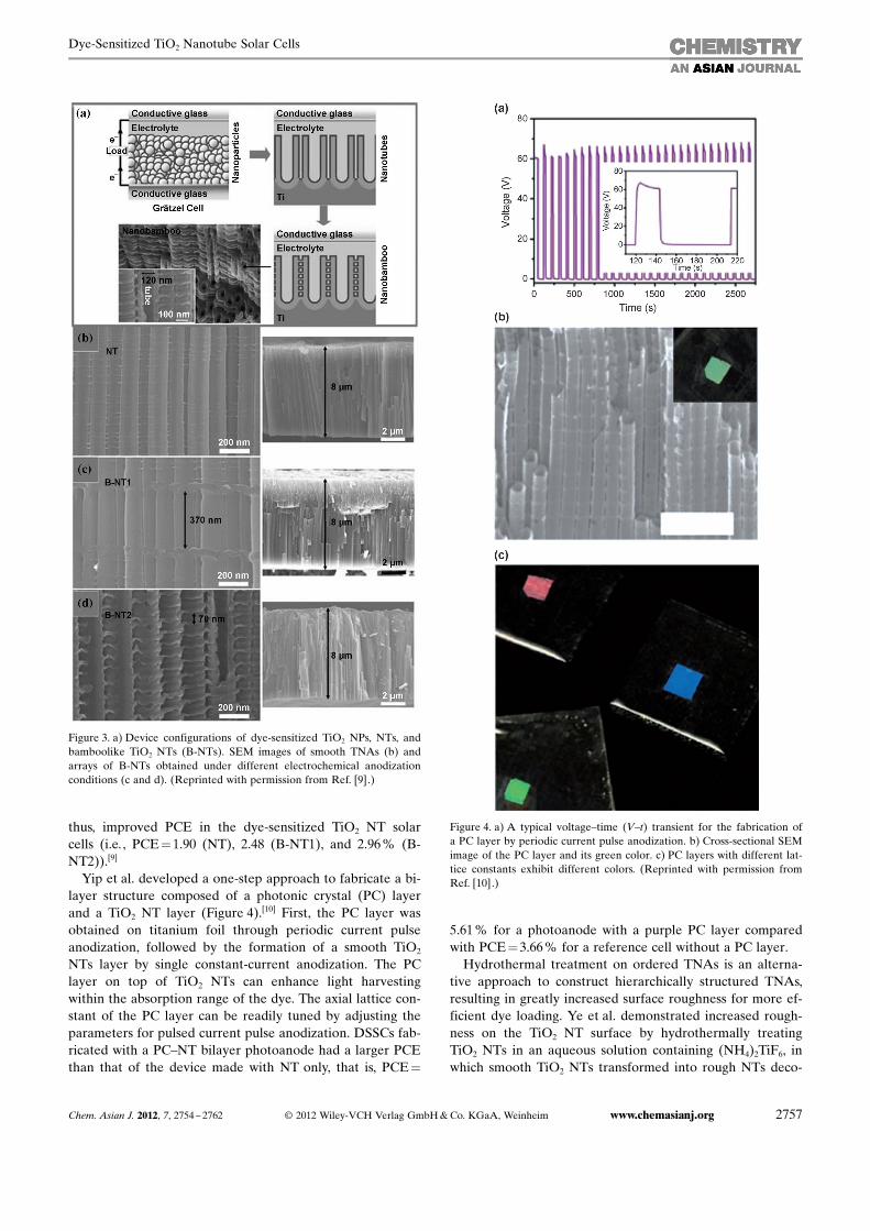
thus, improved PCE in the dye-sensitized TiO2 NT solarcells (i.e. , PCE= 1.90 (NT), 2.48 (B-NT1), and 2.96 % (B-NT2)).[9]
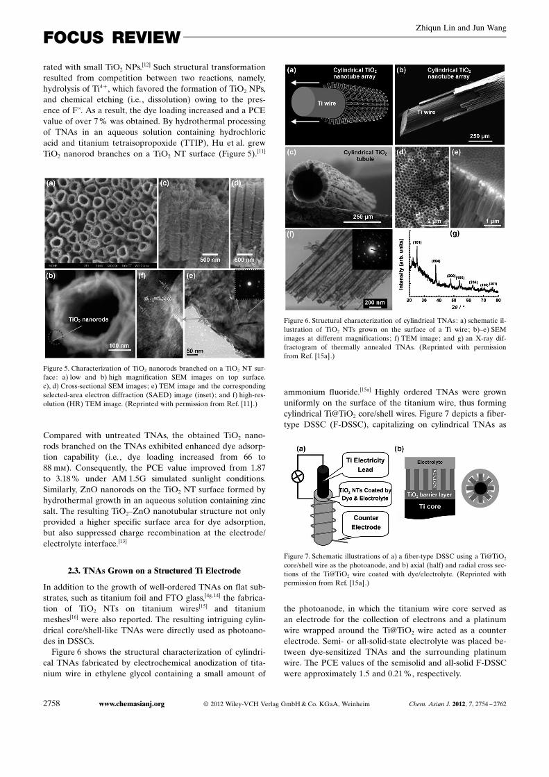
Yip et al. developed a one-step approach to fabricate a bi-layer structure composed of a photonic crystal (PC) layerand a TiO2 NT layer (Figure 4).[10] First, the PC layer wasobtained on titanium foil through periodic current pulseanodization, followed by the formation of a smooth TiO2
NTs layer by single constant-current anodization. The PClayer on top of TiO2 NTs can enhance light harvestingwithin the absorption range of the dye. The axial lattice con-stant of the PC layer can be readily tuned by adjusting theparameters for pulsed current pulse anodization. DSSCs fab-ricated with a PC–NT bilayer photoanode had a larger PCEthan that of the device made with NT only, that is, PCE=
5.61 % for a photoanode with a purple PC layer comparedwith PCE= 3.66 % for a reference cell without a PC layer.
Hydrothermal treatment on ordered TNAs is an alterna-tive approach to construct hierarchically structured TNAs,resulting in greatly increased surface roughness for more ef-ficient dye loading. Ye et al. demonstrated increased rough-ness on the TiO2 NT surface by hydrothermally treatingTiO2 NTs in an aqueous solution containing (NH4)2TiF6, inwhich smooth TiO2 NTs transformed into rough NTs deco-
Figure 3. a) Device configurations of dye-sensitized TiO2 NPs, NTs, andbamboolike TiO2 NTs (B-NTs). SEM images of smooth TNAs (b) andarrays of B-NTs obtained under different electrochemical anodizationconditions (c and d). (Reprinted with permission from Ref. [9].)
Figure 4. a) A typical voltage–time (V–t) transient for the fabrication ofa PC layer by periodic current pulse anodization. b) Cross-sectional SEMimage of the PC layer and its green color. c) PC layers with different lat-tice constants exhibit different colors. (Reprinted with permission fromRef. [10].)
Chem. Asian J. 2012, 7, 2754 – 2762 � 2012 Wiley-VCH Verlag GmbH & Co. KGaA, Weinheim www.chemasianj.org 2757
Dye-Sensitized TiO2 Nanotube Solar Cells
rated with small TiO2 NPs.[12] Such structural transformationresulted from competition between two reactions, namely,hydrolysis of Ti4+ , which favored the formation of TiO2 NPs,and chemical etching (i.e. , dissolution) owing to the pres-ence of F�. As a result, the dye loading increased and a PCEvalue of over 7 % was obtained. By hydrothermal processingof TNAs in an aqueous solution containing hydrochloricacid and titanium tetraisopropoxide (TTIP), Hu et al. grewTiO2 nanorod branches on a TiO2 NT surface (Figure 5).[11]
Compared with untreated TNAs, the obtained TiO2 nano-rods branched on the TNAs exhibited enhanced dye adsorp-tion capability (i.e., dye loading increased from 66 to88 mm). Consequently, the PCE value improved from 1.87to 3.18 % under AM 1.5G simulated sunlight conditions.Similarly, ZnO nanorods on the TiO2 NT surface formed byhydrothermal growth in an aqueous solution containing zincsalt. The resulting TiO2–ZnO nanotubular structure not onlyprovided a higher specific surface area for dye adsorption,but also suppressed charge recombination at the electrode/electrolyte interface.[13]
2.3. TNAs Grown on a Structured Ti Electrode
In addition to the growth of well-ordered TNAs on flat sub-strates, such as titanium foil and FTO glass,[4g,14] the fabrica-tion of TiO2 NTs on titanium wires[15] and titaniummeshes[16] were also reported. The resulting intriguing cylin-drical core/shell-like TNAs were directly used as photoano-des in DSSCs.
Figure 6 shows the structural characterization of cylindri-cal TNAs fabricated by electrochemical anodization of tita-nium wire in ethylene glycol containing a small amount of
ammonium fluoride.[15a] Highly ordered TNAs were grownuniformly on the surface of the titanium wire, thus formingcylindrical Ti@TiO2 core/shell wires. Figure 7 depicts a fiber-type DSSC (F-DSSC), capitalizing on cylindrical TNAs as
the photoanode, in which the titanium wire core served asan electrode for the collection of electrons and a platinumwire wrapped around the Ti@TiO2 wire acted as a counterelectrode. Semi- or all-solid-state electrolyte was placed be-tween dye-sensitized TNAs and the surrounding platinumwire. The PCE values of the semisolid and all-solid F-DSSCwere approximately 1.5 and 0.21 %, respectively.
Figure 5. Characterization of TiO2 nanorods branched on a TiO2 NT sur-face: a) low and b) high magnification SEM images on top surface.c), d) Cross-sectional SEM images; e) TEM image and the correspondingselected-area electron diffraction (SAED) image (inset); and f) high-res-olution (HR) TEM image. (Reprinted with permission from Ref. [11].)
Figure 6. Structural characterization of cylindrical TNAs: a) schematic il-lustration of TiO2 NTs grown on the surface of a Ti wire; b)–e) SEMimages at different magnifications; f) TEM image; and g) an X-ray dif-fractogram of thermally annealed TNAs. (Reprinted with permissionfrom Ref. [15a].)
Figure 7. Schematic illustrations of a) a fiber-type DSSC using a Ti@TiO2
core/shell wire as the photoanode, and b) axial (half) and radial cross sec-tions of the Ti@TiO2 wire coated with dye/electrolyte. (Reprinted withpermission from Ref. [15a].)
2758 www.chemasianj.org � 2012 Wiley-VCH Verlag GmbH & Co. KGaA, Weinheim Chem. Asian J. 2012, 7, 2754 – 2762
FOCUS REVIEWZhiqun Lin and Jun Wang
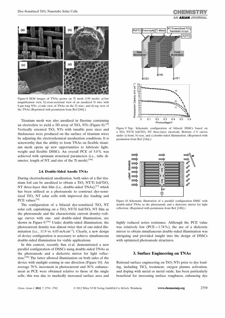
Titanium mesh was also anodized in fluorine containingan electrolyte to yield a 3D array of TiO2 NTs (Figure 8).[16]
Vertically oriented TiO2 NTs with tunable pore sizes andthicknesses were produced on the surface of titanium wiresby adjusting the electrochemical anodization conditions. It isnoteworthy that the ability to form TNAs on flexible titani-um mesh opens up new opportunities to fabricate light-weight and flexible DSSCs. An overall PCE of 5.0 % wasachieved with optimum structural parameters (i.e., tube di-ameter, length of NT, and size of the Ti mesh).[16b]
2.4. Double-Sided Anodic TNAs
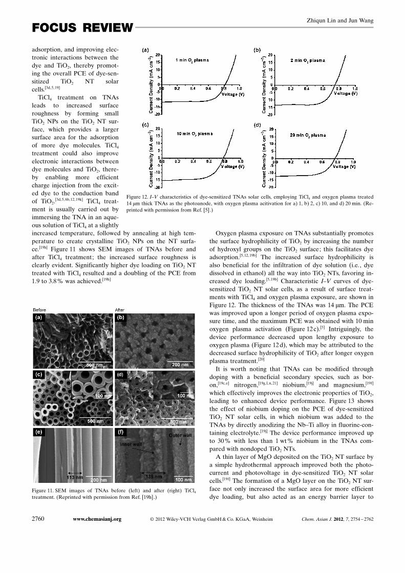
During electrochemical anodization, both sides of a flat tita-nium foil can be anodized to obtain a TiO2 NT/Ti foil/TiO2
NT three-layer thin film (i.e. , double-sided TNAs),[17] whichhas been utilized as a photoanode to construct dye-sensi-tized TiO2 NT solar cells with improved dye loading andPCE values.[18]
The configuration of a bifacial dye-sensitized TiO2 NTsolar cell, capitalizing on a TiO2 NT/Ti foil/TiO2 NT film asthe photoanode and the characteristic current density–volt-age curves with one- and double-sided illumination, areshown in Figure 9.[18a] Under double-sided illumination, thephotocurrent density was almost twice that of one-sided illu-mination (i.e., 11.9 vs. 6.05 mAcm�2). Clearly, a new designof device configuration is necessary to achieve simultaneousdouble-sided illumination for viable applications.
In this context, recently Sun et al. demonstrated a newparallel configuration of DSSCs using double-sided TNAs asthe photoanode and a dielectric mirror for light reflec-tion.[18b] The latter allowed illumination on both sides of thedevice with sunlight coming in one direction (Figure 10). Anaverage 70 % increment in photocurrent and 30 % enhance-ment in PCE were obtained relative to those of the singlecells; this was due to markedly increased surface area and
highly reduced series resistance. Although the PCE valuewas relatively low (PCE= 1.74 %), the use of a dielectricmirror to obtain simultaneous double-sided illumination wasintriguing and provided insight into the design of DSSCswith optimized photoanode structures.
3. Surface Engineering on TNAs
Rational surface engineering on TiO2 NTs prior to dye load-ing, including TiCl4 treatment, oxygen plasma activation,and doping with metal or metal oxide, has been particularlybeneficial for increasing surface roughness, enhancing dye
Figure 8. SEM images of TNAs grown on Ti mesh (150 mesh): a) lowmagnification view; b) cross-sectional view of an anodized Ti wire with8 mm long NTs; c) side view of TNAs on the Ti wire; and d) top view ofthe TNAs (Reprinted with permission from Ref [16b].)
Figure 9. Top: Schematic configuration of bifacial DSSCs based ona TiO2 NT/Ti foil/TiO2 NT three-layer electrode. Bottom: J–V curvesunder a) front, b) rear, and c) double-sided illumination. (Reprinted withpermission from Ref. [18a].)
Figure 10. Schematic illustration of a parallel configuration DSSC withdouble-sided TNAs as the photoanode and a dielectric mirror for lightreflection. (Reprinted with permission from Ref. [18b].)
Chem. Asian J. 2012, 7, 2754 – 2762 � 2012 Wiley-VCH Verlag GmbH & Co. KGaA, Weinheim www.chemasianj.org 2759
Dye-Sensitized TiO2 Nanotube Solar Cells
adsorption, and improving elec-tronic interactions between thedye and TiO2, thereby promot-ing the overall PCE of dye-sen-sitized TiO2 NT solarcells.[3d,5, 19]
TiCl4 treatment on TNAsleads to increased surfaceroughness by forming smallTiO2 NPs on the TiO2 NT sur-face, which provides a largersurface area for the adsorptionof more dye molecules. TiCl4
treatment could also improveelectronic interactions betweendye molecules and TiO2, there-by enabling more efficientcharge injection from the excit-ed dye to the conduction bandof TiO2.
[3d,5,6b, 12,19k] TiCl4 treat-ment is usually carried out byimmersing the TNA in an aque-ous solution of TiCl4 at a slightlyincreased temperature, followed by annealing at high tem-perature to create crystalline TiO2 NPs on the NT surfa-ce.[19h] Figure 11 shows SEM images of TNAs before andafter TiCl4 treatment; the increased surface roughness isclearly evident. Significantly higher dye loading on TiO2 NTtreated with TiCl4 resulted and a doubling of the PCE from1.9 to 3.8 % was achieved.[19h]
Oxygen plasma exposure on TNAs substantially promotesthe surface hydrophilicity of TiO2 by increasing the numberof hydroxyl groups on the TiO2 surface; this facilitates dyeadsorption.[5,12,19b] The increased surface hydrophilicity isalso beneficial for the infiltration of dye solution (i.e., dyedissolved in ethanol) all the way into TiO2 NTs, favoring in-creased dye loading.[5,19b] Characteristic I–V curves of dye-sensitized TiO2 NT solar cells, as a result of surface treat-ments with TiCl4 and oxygen plasma exposure, are shown inFigure 12. The thickness of the TNAs was 14 mm. The PCEwas improved upon a longer period of oxygen plasma expo-sure time, and the maximum PCE was obtained with 10 minoxygen plasma activation (Figure 12 c).[5] Intriguingly, thedevice performance decreased upon lengthy exposure tooxygen plasma (Figure 12 d), which may be attributed to thedecreased surface hydrophilicity of TiO2 after longer oxygenplasma treatment.[20]
It is worth noting that TNAs can be modified throughdoping with a beneficial secondary species, such as bor-on,[19c,e] nitrogen,[19g, l, n,21] niobium,[19j] and magnesium,[19f]
which effectively improves the electronic properties of TiO2,leading to enhanced device performance. Figure 13 showsthe effect of niobium doping on the PCE of dye-sensitizedTiO2 NT solar cells, in which niobium was added to theTNAs by directly anodizing the Nb–Ti alloy in fluorine-con-taining electrolyte.[19j] The device performance improved upto 30 % with less than 1 wt% niobium in the TNAs com-pared with nondoped TiO2 NTs.
A thin layer of MgO deposited on the TiO2 NT surface bya simple hydrothermal approach improved both the photo-current and photovoltage in dye-sensitized TiO2 NT solarcells.[19f] The formation of a MgO layer on the TiO2 NT sur-face not only increased the surface area for more efficientdye loading, but also acted as an energy barrier layer to
Figure 11. SEM images of TNAs before (left) and after (right) TiCl4
treatment. (Reprinted with permission from Ref. [19h].)
Figure 12. I–V characteristics of dye-sensitized TNAs solar cells, employing TiCl4 and oxygen plasma treated14 mm thick TNAs as the photoanode, with oxygen plasma acitivation for a) 1, b) 2, c) 10, and d) 20 min. (Re-printed with permission from Ref. [5].)
2760 www.chemasianj.org � 2012 Wiley-VCH Verlag GmbH & Co. KGaA, Weinheim Chem. Asian J. 2012, 7, 2754 – 2762
FOCUS REVIEWZhiqun Lin and Jun Wang
reduce charge recombination between TiO2 and the electro-lyte.
4. Summary and Outlook
We have highlighted recent efforts to improve the perfor-mance of dye-sensitized TiO2 NT solar cells through rationalstructural and surface engineering on anodic TNAs. A widerange of approaches have been developed to structurallymodify TiO2 NTs, including the integration of TiO2 NPswith NTs, the formation of hierarchically structured TiO2
NTs, the construction of 3D NT arrays on titanium wire andmesh, and a new design of dye-sensitized double-sidedTNAs. Judicious surface engineering on TNAs can be realiz-ed by TiCl4 treatment, oxygen plasma activation, and dopingwith a secondary species. Such advantageous modificationson TNAs have led to significantly improved PCE values inthe resulting dye-sensitized TiO2 NT solar cells. In parallelwith progress being made in seeking the optimization ofdyes, electrolytes, and counter electrodes, these develop-ment activities may yield even higher photovoltaic perform-ances.
Acknowledgements
We gratefully acknowledge support from the Georgia Institute of Tech-nology.
[1] a) B. O�Regan, M. Gr�tzel, Nature 1991, 353, 737 –740; b) M. Gr�t-zel, Nature 2001, 414, 338 –344; c) A. Yella, H. W. Lee, H. N. Tsao,C. Y. Yi, A. K. Chandiran, M. K. Nazeeruddin, E. W. G. Diau, C. Y.Yeh, S. M. Zakeeruddin, M. Gratzel, Science 2011, 334, 629 –634;d) L. M. GonÅalves, V. D. Bermudez, H. A. Ribeiro, A. M. Mendes,Energy Environ. Sci. 2008, 1, 655 –667; e) C. J. Lin, W. Y. Yu, S. H.Chien, J. Mater. Chem. 2010, 20, 1073 –1077.
[2] a) X. Xin, M. He, W. Han, J. Jung, Z. Lin, Angew. Chem. 2011, 123,11943 – 11946; Angew. Chem. Int. Ed. 2011, 50, 11 739 –11 742; b) M.Paulose, K. Shankar, O. K. Varghese, G. K. Mor, B. Hardin, C. A.Grimes, Nanotechnology 2006, 17, 1446; c) K. Zhu, A. J. Frank,MRS Bull. 2011, 36, 446 – 452; d) A. Mishra, M. K. R. Fischer, P.Bauerle, Angew. Chem. 2009, 121, 2510 – 2536; Angew. Chem. Int.Ed. 2009, 48, 2474 –2499; e) L. Han, A. Islam, H. Chen, C. Malapa-ka, B. Chiranjeevi, S. Zhang, X. Yang, M. Yanagida, Energy Envi-ron. Sci. 2012, 5, 6057 – 6060; f) C.-M. Lan, H.-P. Wu, T.-Y. Pan, C.-W. Chang, W.-S. Chao, C.-T. Chen, C.-L. Wang, C.-Y. Lin, E. W.-G.Diau, Energy Environ. Sci. 2012, 5, 6460 –6464; g) D. M. Li, D. Qin,M. H. Deng, Y. H. Luo, Q. B. Meng, Energy Environ. Sci. 2009, 2,283 – 291; h) Z. J. Ning, Y. Fu, H. Tian, Energy Environ. Sci. 2010, 3,1170 – 1181; i) B. O�Regan, L. Xiaoe, T. Ghaddar, Energy Environ.Sci. 2012, 5, 7203 –7215; j) M. Wu, X. Lin, Y. Wang, L. Wang, W.Guo, D. Qi, X. Peng, A. Hagfeldt, M. Gratzel, T. Ma, J. Am. Chem.Soc. 2012, 134, 3419 – 3428; k) J. N. de Freitas, A. F. Nogueira, M. A.De Paoli, J. Mater. Chem. 2009, 19, 5279 –5294; l) L. M. Chen, Z. R.Hong, G. Li, Y. Yang, Adv. Mater. 2009, 21, 1434 –1449; m) H. J.Snaith, L. Schmidt-Mende, Adv. Mater. 2007, 19, 3187 –3200;n) S. M. Zakeeruddin, M. Gratzel, Adv. Funct. Mater. 2009, 19,2187 – 2202.
[3] a) V. Zwilling, M. Aucouturier, E. Darque-Ceretti, Electrochim.Acta 1999, 45, 921 – 929; b) J. Wang, Z. Q. Lin, Chem. Mater. 2008,20, 1257 – 1261; c) O. K. Varghese, D. Gong, M. Paulose, C. A.Grimes, E. C. Dickey, J. Mater. Res. 2003, 18, 156 – 165; d) M. Pau-lose, K. Shankar, S. Yoriya, H. E. Prakasam, O. K. Varghese, G. K.Mor, T. A. Latempa, A. Fitzgerald, C. A. Grimes, J. Phys. Chem. B2006, 110, 16179 – 16184; e) G. K. Mor, O. K. Varghese, M. Paulose,K. Shankar, C. A. Grimes, Sol. Energy Mater. Sol. Cells 2006, 90,2011 – 2075; f) J. M. Macak, H. Tsuchiya, L. Taveira, S. Aldabergero-va, P. Schmuki, Angew. Chem. 2005, 117, 7629 –7632; Angew. Chem.Int. Ed. 2005, 44, 7463 –7465; g) D. Gong, C. A. Grimes, O. K. Var-ghese, W. Hu, R. S. Singh, Z. Chen, E. C. Dickey, J. Mater. Res.2001, 16, 3331 –3334.
[4] a) K. Zhu, N. R. Neale, A. Miedaner, A. J. Frank, Nano Lett. 2007,7, 69– 74; b) K. Zhu, T. B. Vinzant, N. R. Neale, A. J. Frank, NanoLett. 2007, 7, 3739 –3746; c) K. Shankar, G. K. Mor, H. E. Prakasam,S. Yoriya, M. Paulose, O. K. Varghese, C. A. Grimes, Nanotechnolo-gy 2007, 18, 065707; d) A. Kongkanand, K. Tvrdy, K. Takechi, M.Kuno, P. V. Kamat, J. Am. Chem. Soc. 2008, 130, 4007 – 4015; e) M.Paulose, K. Shankar, O. K. Varghese, G. K. Mor, C. A. Grimes, J.Phys. D 2006, 39, 2498 –2503; f) K. Shankar, G. K. Mor, H. E. Pra-kasam, O. K. Varghese, C. A. Grimes, Langmuir 2007, 23, 12445 –12449; g) J. Wang, Z. Q. Lin, J. Phys. Chem. C 2009, 113, 4026 –4030; h) B. X. Lei, J. Y. Liao, R. Zhang, J. Wang, C. Y. Su, D. B.Kuang, J. Phys. Chem. C 2010, 114, 15 228 –15 233.
[5] J. Wang, Z. Q. Lin, Chem. Mater. 2010, 22, 579 – 584.[6] a) Q. Zheng, H. Kang, J. Yun, J. Lee, J. H. Park, S. Baik, ACS Nano
2011, 5, 5088 –5093; b) X. K. Xin, J. Wang, W. Han, M. D. Ye, Z. Q.Lin, Nanoscale 2012, 4, 964 –969.
[7] a) J. G. Chen, C. Y. Chen, C. G. Wu, C. Y. Lin, Y. H. Lai, C. C.Wang, H. W. Chen, R. Vittal, K. C. Ho, J. Mater. Chem. 2010, 20,7201 – 7207; b) Y. H. Chen, K. C. Huang, J. G. Chen, R. Vittal, K. C.Ho, Electrochim. Acta 2011, 56, 7999 – 8004; c) C. Rho, J. S. Suh,Chem. Phys. Lett. 2011, 513, 108 –111; d) Y. Alivov, Z. Y. Fan, Appl.
Figure 13. I–V characteristics of dye-sensitized TiO2 NT solar cells fabri-cated with Nb-doped TiO2 NTs with different annealing temperaturesand concentrations of Nb: a) TiO2 NTs and 0.1 Nb–TiO2 annealed at dif-ferent temperatures; and b) TiO2 NTs doped with different concentra-tions of Nb. (Reprinted with permission from Ref. [19j].)
Chem. Asian J. 2012, 7, 2754 – 2762 � 2012 Wiley-VCH Verlag GmbH & Co. KGaA, Weinheim www.chemasianj.org 2761
Dye-Sensitized TiO2 Nanotube Solar Cells

Phys. Lett. 2009, 95, 063504; e) S. H. Wang, J. B. Zhang, S. Chen,H. T. Yang, Y. Lin, X. R. Xiao, X. W. Zhou, X. P. Li, Electrochim.Acta 2011, 56, 6184 –6188.
[8] J. Wang, L. Zhao, V. S. Y. Lin, Z. Q. Lin, J. Mater. Chem. 2009, 19,3682 – 3687.
[9] D. Kim, A. Ghicov, S. P. Albu, P. Schmuki, J. Am. Chem. Soc. 2008,130, 16454 – 16455.
[10] C. T. Yip, H. T. Huang, L. M. Zhou, K. Y. Xie, Y. Wang, T. H. Feng,J. S. Li, W. Y. Tam, Adv. Mater. 2011, 23, 5624 – 5628.
[11] A. Z. Hu, H. N. Li, Z. Y. Jia, Z. C. Xia, J. Solid State Chem. 2011,184, 2936 –2940.
[12] M. D. Ye, X. K. Xin, C. J. Lin, Z. Q. Lin, Nano Lett. 2011, 11, 3214 –3220.
[13] S. S. Kim, S. I. Na, Y. C. Nah, Electrochim. Acta 2011, 58, 503 – 509.[14] a) G. K. Mor, O. K. Varghese, M. Paulose, C. A. Grimes, Adv. Funct.
Mater. 2005, 15, 1291 –1296; b) A. Z. Sadek, H. Zheng, K. Latham,W. Wlodarski, K. Kalantar-zadeh, Langmuir 2009, 25, 509 –514.
[15] a) J. F. Yu, D. Wang, Y. N. Huang, X. Fan, X. Tang, C. Gao, J. L. Li,D. C. Zou, K. Wu, Nanoscale Res. Lett. 2011, 6, 94; b) S. Q. Huang,X. Z. Guo, X. M. Huang, Q. X. Zhang, H. C. Sun, D. M. Li, Y. H.Luo, Q. B. Meng, Nanotechnology 2011, 22, 315402.
[16] a) Z. Y. Liu, V. Subramania, M. Misra, J. Phys. Chem. C 2009, 113,14028 – 14033; b) C. S. Rustomji, C. J. Frandsen, S. Jin, M. J. Tauber,J. Phys. Chem. B 2010, 114, 14537 – 14543.
[17] H. E. Prakasam, K. Shankar, M. Paulose, O. K. Varghese, C. A.Grimes, J. Phys. Chem. C 2007, 111, 7235 –7241.
[18] a) Z. Y. Liu, M. Misra, Nanotechnology 2010, 21, 125703; b) L. D.Sun, S. Zhang, X. Wang, X. W. Sun, D. Y. Ong, A. K. K. Kyaw,Energy Environ. Sci. 2011, 4, 2240 – 2248.
[19] a) D. Kim, P. Roy, K. Lee, P. Schmuki, Electrochem. Commun. 2010,12, 574 –578; b) R. Liu, W. D. Yang, L. S. Qiang, J. Power Sources2012, 199, 418 –425; c) N. Lu, H. M. Zhao, J. Y. Li, X. Quan, S.Chen, Sep. Purif. Technol. 2008, 62, 668 – 673; d) J. H. Park, J. Y.Kim, J. H. Kim, C. J. Choi, H. Kim, Y. E. Sung, K. S. Ahn, J. PowerSources 2011, 196, 8904 –8908; e) H. J. Tian, L. H. Hu, C. N. Zhang,S. H. Chen, J. A. Sheng, L. Mo, W. Q. Liu, S. Y. Dai, J. Mater. Chem.2011, 21, 863 –868; f) H. Park, D. J. Yang, H. G. Kim, S. J. Cho, S. C.Yang, H. Lee, W. Y. Choi, J. Electroceram. 2009, 23, 146 –149;g) H. J. Wu, Z. H. Zhang, Int. J. Hydrogen Energy 2011, 36, 13481 –13487; h) P. Roy, D. Kim, I. Paramasivam, P. Schmuki, Electrochem.Commun. 2009, 11, 1001 – 1004; i) P. Charoensirithavorn, Y. Ogomi,T. Sagawa, S. Hayase, S. Yoshikawaa, J. Electrochem. Soc. 2010, 157,B354 –B356; j) M. Yang, D. Kim, H. Jha, K. Lee, J. Paul, P. Schmu-ki, Chem. Commun. 2011, 47, 2032 –2034; k) X. K. Xin, M. Scheiner,M. D. Ye, Z. Q. Lin, Langmuir 2011, 27, 14594 –14598; l) Q. Y.Wang, X. C. Yang, X. L. Wang, M. Huang, J. W. Hou, Electrochim.Acta 2012, 62, 158 –162; m) Y. Y. Zhang, X. J. Li, M. Z. Feng, F. L.Zhou, J. Z. Chen, Surf. Coat. Technol. 2010, 205, 2572 –2577; n) J. J.Xu, Y. H. Ao, M. D. Chen, D. G. Fu, Appl. Surf. Sci. 2010, 256,4397 – 4401.
[20] D. Lu, Y. Wu, J. H. Guo, G. Lu, Y. Wang, J. C. Shen, Mater. Sci.Eng. B 2003, 97, 141 –144.
[21] X. Liu, Z. Q. Liu, J. Zheng, X. Yan, D. D. Li, S. Chen, W. Chu, J.Alloys Compd. 2011, 509, 9970 –9976.
Received: April 17, 2012Revised: May 9, 2012
Published online: June 18, 2012
2762 www.chemasianj.org � 2012 Wiley-VCH Verlag GmbH & Co. KGaA, Weinheim Chem. Asian J. 2012, 7, 2754 – 2762
FOCUS REVIEWZhiqun Lin and Jun Wang