dynamic electronic doping for correlated oxides by a ... · 2018 wiley-vch verlag gmbh & co....
TRANSCRIPT

CommuniCation
1803580 (1 of 8) © 2018 WILEY-VCH Verlag GmbH & Co. KGaA, Weinheim
www.advmat.de
Dynamic Electronic Doping for Correlated Oxides by a Triboelectric Nanogenerator
Yuliang Chen, Ying Zhang, Zhaowu Wang, Taotao Zhan, Yi-Cheng Wang, Haiyang Zou, Hui Ren, Guobin Zhang, Chongwen Zou,* and Zhong Lin Wang*
DOI: 10.1002/adma.201803580
External stimuli are commonly used to adjust materials’ properties to achieve var-ious functionalities. Some typical examples include applying gate voltage for field-effect transistors (FETs),[1] using magnetic field for spintronics,[2] and employing force field on piezotronics.[3,4] Metal–insu-lator transition (MIT) in some transition metal oxides is a distinct feature that is being used for the development of various electronic devices due to it can poten-tially lead to outstanding on–off ratio,[5] spin–orbit coupling,[6] or even the possible superconductivity.[7,8]
As a typical correlated metal oxide, vana-dium dioxide (VO2) shows a pronounced MIT behavior from low-temperature insulator (M1) phase to high temperature metallic (R) phase. Across the phase tran-sition, it will undergo a sharp resistance change, up to five orders of magnitude, and a pronounced infrared switching effect within sub-ps time scale.[9–12] In addition to the excellent phase transition
The metal–insulator transition of vanadium dioxide (VO2) is exceptionally sensitive to charge density and electron orbital occupancy. Thus three-terminal field-effect transistors with VO2 channels are widely adopted to control the phase transition by external gating voltage. However, current leakage, electrical breakdown, or interfacial electrochemical reactions may be inevitable if conventional solid dielectrics or ionic-liquid layers are used, which possibly induce Joule heating or doping in the VO2 layer and make the voltage-controlled phase transition more complex. Here, a triboelectric nanogenerator (TENG) and a VO2 film are combined for a novel TENG-VO2 device, which can overcome the abovementioned challenges and achieve electron-doping-induced phase modulation. By taking advantage of the TENG structure, electrons can be induced in the VO2 channel and thus adjust the electronic states of the VO2, simultaneously. The modulation degree of the VO2 resistance depends on the temperature, and the major variation occurs when the temperature is in the phase-transition region. The accumulation of electrons in the VO2 channel also is simulated by finite element analysis, and the electron doping mechanism is verified by theoretical calculations. The results provide a promising approach to develop a novel type of tribotronic transistor and new electronic doping technology.
Phase Modulation
Y. L. Chen, Prof. Y. Zhang, Prof. Y.-C. Wang, H. Y. Zou, Prof. Z. L. WangSchool of Materials Science and EngineeringGeorgia Institute of TechnologyAtlanta, GA 30332-0245, USAE-mail: [email protected]. L. Chen, H. Ren, Prof. G. B. Zhang, Prof. C. W. ZouNational Synchrotron Radiation LaboratoryUniversity of Science and Technology of ChinaHefei 230029, ChinaE-mail: [email protected]. Y. Zhang, T. T. ZhanKey Laboratory of Thermo-Fluid Science and EngineeringMinistry of EducationXi’an Jiaotong UniversityXi’an 710049, ChinaDr. Z. W. WangSchool of Physics and EngineeringHenan Key Laboratory of Photoelectric Energy Storage Materials and ApplicationsHenan University of Science and TechnologyLuoyang 471023, China
Dr. Z. W. WangNational Laboratory of Solid State MicrostructuresNanjing UniversityNanjing 210093, ChinaProf. Y.-C. WangDepartment of Food Science and Human NutritionUniversity of Illinois at Urbana-ChampaignUrbana, IL 61801, USAProf. Z. L. WangBeijing Institute of Nanoenergy and NanosystemsChinese Academy of SciencesBeijing 100085, ChinaProf. Z. L. WangCollege of Nanoscience and TechnologyUniversity of Chinese Academy of SciencesBeijing 100049, China
The ORCID identification number(s) for the author(s) of this article can be found under https://doi.org/10.1002/adma.201803580.
Adv. Mater. 2018, 1803580
© 2018 WILEY-VCH Verlag GmbH & Co. KGaA, Weinheim1803580 (2 of 8)
www.advmat.dewww.advancedsciencenews.com
induced electronic or optical properties, VO2 has extra advan-tages comparing with other phase transition oxides: simple binary oxide with a critical temperature (≈340 K) close to room temperature. All of these distinct properties make VO2 a prom-ising candidate for many applications such as thermal sen-sors, smart windows, phase transition memories, or ultrafast response optical devices.[13–15]
However, the relatively high transition temperature of VO2 crystal is still a bottleneck for its practical applications at room temperature. Thus, various methods have been attempted to modulate the MIT process as well as decrease its critical tem-perature.[16–20] It has been reported that gating a VO2-layer-based FETs with SiO2, TiO2, or HfO2 dielectrics can modulate the phase transitions. For example, Sengupta et al. observed a reversible and hysteretic conductance change (≈6%) induced by a gate voltage when HfO2 was used as the dielectric layer in the VO2-layer-based FETs.[21] Yajima et al. achieved a positive-bias gate-controlled metal–insulator transition via a high-permittivity TiO2 gate dielectric.[22] For these conventional transistor devices, the electric field driven charge density is not high enough to trigger the completed phase transitions at room temperature. In addition, the current leakage or electrical breakdown induced local Joule heating may be involved in the field-induced phase transitions, which makes the real mecha-nism much more complex. Due to the high gating charge den-sity at the interface, ionic liquid (IL) dielectrics are frequently adopted for the VO2-based FET devices recently.[23] However, the unavoidable impurities such as residual water, hydroxide, and oxycarbide in IL may induce the hydrogen doping or oxygen vacancies due to the interfacial electrochemical reaction rather than the expected pure electrostatic effect.[24–26]
Considering the gating model on the dielectric IL layer, we found that the electrostatic effect induced charge separation was very similar to the basic operation principle of triboelectric nanogenerator (TENG)—separation of opposite charges plus electric induction.[27–30] TENG is a kind of device that can con-vert ambient mechanical energy to electrical output, taking advantage of contact electrification and electrical induction. As the mechanical energy is ubiquitous in our daily life, such as vibration, breeze, and water wave, they can be effectively har-vested by various TENGs. Since it was first proposed by Wang’s group in 2012,[31] numerous novel devices based on TENG have been developed, such as self-powered electronics, blue energy harvesting, and vibration sensors.[32–38]
Accordingly, in this work, we combine a TENG device with VO2 film to develop a correlated three-terminal device (TENG-VO2). In this configuration, the VO2 film and TENG serve as the channel and gate, respectively.[39] The electrons will be induced in VO2 channel due to the triboelectric effect plus elec-tric induction, which can change the electronic state of VO2, simultaneously. In addition, it shows that the electron doping induced resistance change of VO2 layer is strongly depending on the temperature, and the more pronounced resistance vari-ation occurs within the phase transition region (PTR) of the VO2. The electrons accumulation in VO2 channel is simulated by finite element analysis (FEA), which further confirms the triboelectric effect on the VO2 phase modulation. Detailed first-principle calculations validate the electrons doping effect on the phase transition of VO2 crystal. Our current study not only
demonstrates the electron doping induced phase modulation of VO2 material but also leads to a new way of expanding the TENG for tribotronic transistors and novel electron doping technologies.
Figure 1a,b shows the configurations for the IL assisted FET device and TENG-VO2 device, respectively. The equivalent circuit for IL assisted FET device can be considered as three resistor-capacitor (RC) units in series: two RCs for the electric double layers (EDL) interfaces at the electrodes and one for the bulk IL phase.[40] EDL can induce electrons on the channel surface and realize electron doping if applying positive gating voltage within the electrochemical potential windows.[41] Ideally, the IL layer can be considered as an absolute insulator. How-ever, due to the existence of impurities (e.g., residual water, and hydroxide) in actual experiments, the interfacial electrochem-ical reactions could be triggered. While for the FET based on TENG, negative and positive charges will be separated between the two dielectric surfaces after contact due to the different triboelectric properties.[42] The bottom mechanism seems to associate with the surface potential barrier, the work function, or the molecular-scale fluctuations.[43–45] After separating the two dielectric layers of TENG-based FET, the opposite charges are induced respectively on metal electrode and VO2 channel simultaneously. In the shown equivalent circuit (Figure 1b), there is no resistor involved due to the insulating properties of dielectric materials and air gap, which indicates the TENG-VO2 structure could avoid the possible electrochemical doping and current leakage.
The actual fabricated device (TENG-VO2) is shown in Figure 1c. Specifically, we use gold electrodes, a copper film, a poly(tetrafluoroethylene) (PTFE) layer, a nylon layer, and a VO2 film to fabricate the three-terminal FET device. An ohmmeter is used to record the whole channel resistance in real time. The working processes are summarized as the following steps: I) In the triboelectric structural part, when the PTFE and nylon layers (two dielectric layers) are in contact with each other, neg-ative charges would transfer from nylon surface to PTFE sur-face.[42] The separation distance between two dielectric layers is in atomic scale at this moment, and the two opposite charges electrostatic screening each other results in no charges being induced on the copper film and the VO2 channel. II) Increasing the separation distance between two dielectric layers could weaken the electrostatic screening effect. Then the positive charges (holes) on copper film and negative charges (electrons) on the VO2 channel would be induced. III) Further increasing the distance would induce more charges to balance the electric field. IV) Reducing the distance between two dielectric layers, the previously induced electrons in the VO2 channels would go back to the copper film. Finally, when these two dielectric materials contact with each other again, there is no any induced charge on VO2 channel and a cycle is completed.
Accordingly, by integrating a TENG with a VO2 channel, the TENG can effectively change the charge amount in the VO2 channel during its working processes. As a strongly cor-related oxide material, the phase transition behavior of VO2 is always sensitive to its carrier density. Thus, the VO2 properties in the FET configuration can be adjusted and directly moni-tored by the electrical measurement as shown in the following sections.
Adv. Mater. 2018, 1803580

© 2018 WILEY-VCH Verlag GmbH & Co. KGaA, Weinheim1803580 (3 of 8)
www.advmat.dewww.advancedsciencenews.com
Figure 2a shows the typical resistance–temperature curve for a 30 nm VO2 film deposited on a c-cut Al2O3 substrate (Figure S1, Supporting Information). The related derivative curve in Figure 2b shows the critical temperature (Tc) value of 339.3 K for the heating process, with a PTR about 12 K width. The designed operation scheme (one cycle) of the TENG structure for under-standing the electric properties of VO2 is shown in Figure 2c. First, the PTFE and nylon layers are separated at the distance of 40 mm for 10 s. Then, the two layers are in contact with each other for another 10 s. After the first contact-separation event of TENG, at the initial separated situation, the induced electrons appear on VO2 channel, whereas, when the two dielectric layers are forced to touch each other, the induced electrons will be depleted completely (inset of Figure 2c).
Figure 2d–h shows the resistance measurements for the selected five temperature points (A–E) (additional results can be found in Figure S2, Supporting Information). It can be observed that the designed TENG operation (Figure 2c) can induce distinct resistance variations. The magnitude of the
resistance change is various at different temperatures, com-pared with each initial resistance value. The ratio of high resist-ance (RH) and low resistance (RL) is further used to estimate the modulation degree as shown in Figure 2i. As can be seen from the figure, at A or E point, which temperature is relatively far from the critical temperature (339.3 K, according to Figure 2b), the ratio of resistance (RH/RL) is almost equal to one. This means that the resistance change is negligible. As the tempera-ture is getting close to the PTR, the modulation effect becomes more remarkable, which reaches a peak (574%) value at 337.6 K that closes to the Tc. Comparing Figure 2b with Figure 2i, the trend of the modulation degree versus temperatures coin-cides with that of the PTR of VO2. In addition, similar results are also observed when PTFE layer is separating from nylon (after contacting) (Figure S3, Supporting Information), further confirming the modulation effect from the integrated TENG structure.
To further examine the dynamic modulation on VO2 channel, we continuously change the separated distance in
Adv. Mater. 2018, 1803580
Figure 1. Schematics and corresponding equivalent circuits with VO2 film as the channel for: a) ionic liquid (IL)-assisted structure, and b) TENG structure, respectively. c) The elements of the fabricated TENG-VO2 device and its working principle. The induced electrons appear and vanish in VO2 channel controlled by contact and separation between PTFE and nylon.

© 2018 WILEY-VCH Verlag GmbH & Co. KGaA, Weinheim1803580 (4 of 8)
www.advmat.dewww.advancedsciencenews.com
the following three steps (route: 40 mm → 3 mm → 0 mm) as shown in Figure 3a. The recorded charge (baseline is the meas-urement obtained at the separated distance of 0 mm) curve shows three plateaus, which suggests the electrons could grad-ually flow from the VO2 channel to the copper electrode during the approaching of the two dielectric layers (PTFE and nylon layers). As a result, the VO2 resistance curve recorded at a tem-perature closed to Tc shows three corresponding plateaus due to the decreasing electron density as shown in Figure 3b.
The relationship of the amount of induced electrons in VO2 channel versus the separation distance between PTFE and nylon layers is simulated by FEA. The curve of Figure 3c shows the simulated results for the relationship between the transferred charges and separation distance, which confirms the that additional induced electrons will flow into(out) the VO2 channel by increasing(reducing) the separation distance between the two dielectric layers. It is worth pointing out that the charge–distance curve in Figure 3c is not a linear one, e.g.,
most of the induced electrons will be transferred at shorter separated distances, for example, about 71.7% of the electrons are transferred as the separation distance between PTFE and nylon is shorter than 7.5 mm (yellow region in Figure 3c). This nonlinear charge transfer phenomenon can be also observed in the electrical measurements of other TENG devices, such as the short-circuit current peaks or open-circuit voltage peaks.[28,46,47] The green stars in Figure 3c are the measured data derived from Figure 3a, which are well consistent with the simulation curve. The simulation results of the potential distribution of the TENG-VO2 device are presented in Figure S4 in the Supporting Information.
In addition, we observed the maximum transferred charge increased when the current TENG-VO2 device was heated, although the increment is not explosive compared with that at room temperature (Figure S5a, Supporting Information). As a controlled experiment, the electrical output of a regular TENG with two metal electrodes (i.e., PTFE/Cu and nylon/Cu) was
Adv. Mater. 2018, 1803580
Figure 2. a) The resistance-temperature curve of VO2 channel, suggesting metal–insulator transition (MIT) was up to three orders of magnitude. The five red circles (A–E) were adopted to conduct the following experiments of resistance adjustment by contact and separation of PTFE and nylon in the TENG device. b) The related derivative curve of resistance–temperature. The phase transition region (PTR) of VO2 is about 12 K around Tc (339.3 K). c) The designed experimental operation of TENG: maintaining the PTFE and nylon separated at 40 mm for 10 s, then make the two layers in contact with each other. d–h) The five sets of resistance variation experiments (A–E in Figure 2a) of VO2 channel using the designed experimental operation (Figure 2c). i) The ratio of high resistance (RH) and low resistance (RL) at different temperature points, indicating the adjusted degree is more remarkable in the PTR.

© 2018 WILEY-VCH Verlag GmbH & Co. KGaA, Weinheim1803580 (5 of 8)
www.advmat.dewww.advancedsciencenews.com
measured at different temperatures. On the contrary, the results for the regular TENG show that the maximum transferred charge almost kept constant (Figure S5b, Supporting Informa-tion). The increment of the maximum transferred charge at ele-vated temperature for the TENG-VO2 device could be attributed to the MIT of VO2. It should be pointed out that the resistance value is ≈102 Ω of a metallic VO2 and ≈106 Ω for an insulator VO2 (Figure 2a) respectively, while the TENG’s internal resist-ance value (with the air gap) is up to 108–109 Ω. Therefore, the TENG’s internal resistance plays a dominating role to govern the maximum transferred charge,[28,48] i.e., the increment of the maximum transferred charge at high temperature is slight for the current TENG-VO2 device (details in Note S1, Supporting Information). Based on this TENG-VO2 device, we also simu-lated the charge density distribution of VO2 channel with different separation distances between two dielectric layers (Figure 3d). It can be observed that larger distance will lead to a higher charge density distribution up to 1010–1011 cm−2.
According to the previous report,[49] the theoretical electron density for triggering the VO2 phase transition at room tem-perature should be up to 1013 cm−2 or higher. While in our experiments, the produced electron density by TENG is lower than the theoretical value, thus, no pronounced adjusted effect (the “A” point in Figure 2a) is observed at room temperature. However, when increasing the temperature close to the Tc of the VO2, the energy barrier for phase transition (from M1 to R phase) will become lower or perhaps the intermediate phase structure (for example, M2 phase) will appear.[50,51] Under this
elevated temperature condition, even a small amount of charge density variation should be enough to adjust the phase transi-tion as shown in Figure 2.
It is worth noting that the simulated average charge density distribution in VO2 channel in Figure 3d is an ideal situation without considering the surface (micro- or nano-)morphology. While considering the contact interface between the VO2 channel and flexible nylon layer, the individual actual con-tacting area could be a dot with nanoscale or microscale. There-fore, for the actual contact regions in VO2 channel, the local injected charge density could be higher than 1011 cm−2 and even enough to drive the phase transition. In addition, the actually required electron density to drive the phase transi-tion could probably be lower than the theoretical value, since the coexisted phase structures or the phase separation in PTR arising from the possible microstrain, oxygen vacancy, impu-rity, or local crystal defects in the prepared VO2 may result in lower phase transition barrier.[52] In fact, comparing our TENG-VO2 device with the traditional VO2-based FET structure with TiO2 gate dielectrics,[22] the decreasing trend of VO2 channel resistance is almost same by reducing the gating voltage or by decreasing the separated distance.
To gain insights into the charge-doping-driven MIT mecha-nism, we performed first-principles simulations at the density functional theory (DFT) level to examine the charge induced electronic structure variations. For M1 VO2 unit cell, the doping of electrons induces subtle geometric variations including slightly enhanced lattice parameters and expanded cell volumes,
Adv. Mater. 2018, 1803580
Figure 3. a) By reducing the separation distance between the PTFE and the nylon in three steps (route: 40 mm → 3 mm → 0 mm), there are three plateaus of transferred charge (b) and three corresponding plateaus appear in the resistance variation of the VO2 channel. c) The orange line is the relation-ship of the amount of induced electrons in VO2 channel versus the separated distance between PTFE and nylon simulated by finite element analysis (FEA). Most of the induced electrons are transferred when the separation distance is smaller than 7.5 mm (yellow region). The green stars are the experimental results of Figure 2a, which well coincide with the simulated line. d) The charge density distribution of VO2 channel at different distances simulated by FEA.
© 2018 WILEY-VCH Verlag GmbH & Co. KGaA, Weinheim1803580 (6 of 8)
www.advmat.dewww.advancedsciencenews.com
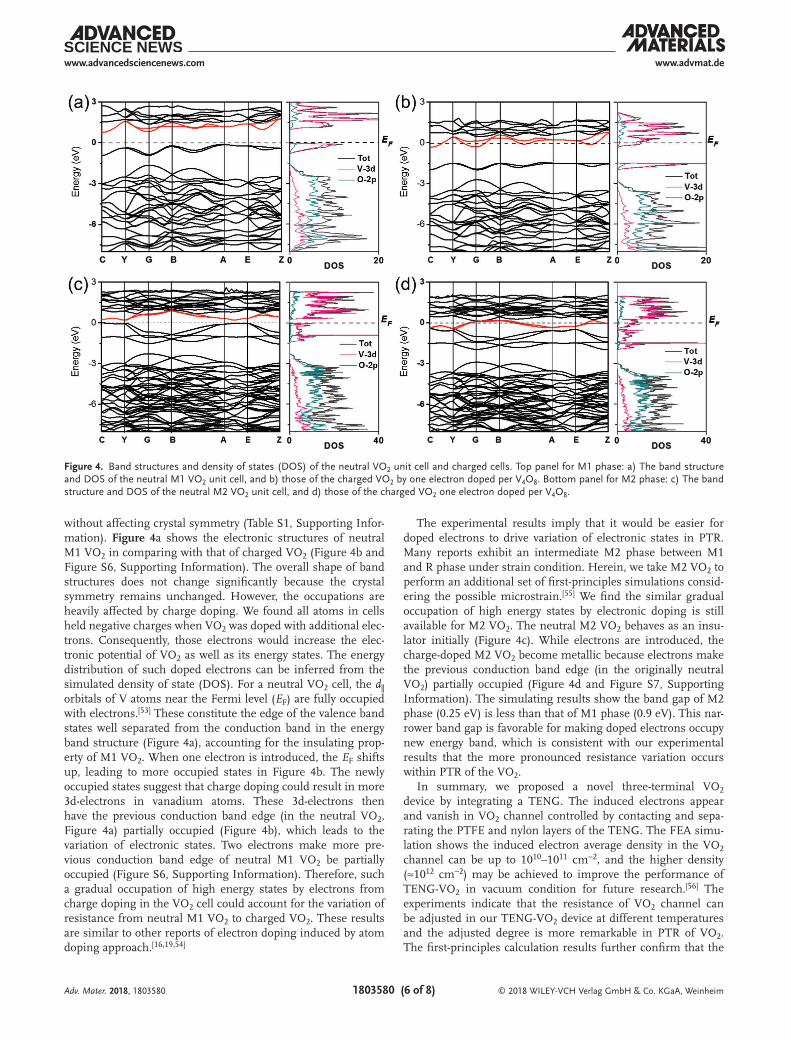
without affecting crystal symmetry (Table S1, Supporting Infor-mation). Figure 4a shows the electronic structures of neutral M1 VO2 in comparing with that of charged VO2 (Figure 4b and Figure S6, Supporting Information). The overall shape of band structures does not change significantly because the crystal symmetry remains unchanged. However, the occupations are heavily affected by charge doping. We found all atoms in cells held negative charges when VO2 was doped with additional elec-trons. Consequently, those electrons would increase the elec-tronic potential of VO2 as well as its energy states. The energy distribution of such doped electrons can be inferred from the simulated density of state (DOS). For a neutral VO2 cell, the d|| orbitals of V atoms near the Fermi level (EF) are fully occupied with electrons.[53] These constitute the edge of the valence band states well separated from the conduction band in the energy band structure (Figure 4a), accounting for the insulating prop-erty of M1 VO2. When one electron is introduced, the EF shifts up, leading to more occupied states in Figure 4b. The newly occupied states suggest that charge doping could result in more 3d-electrons in vanadium atoms. These 3d-electrons then have the previous conduction band edge (in the neutral VO2, Figure 4a) partially occupied (Figure 4b), which leads to the variation of electronic states. Two electrons make more pre-vious conduction band edge of neutral M1 VO2 be partially occupied (Figure S6, Supporting Information). Therefore, such a gradual occupation of high energy states by electrons from charge doping in the VO2 cell could account for the variation of resistance from neutral M1 VO2 to charged VO2. These results are similar to other reports of electron doping induced by atom doping approach.[16,19,54]
The experimental results imply that it would be easier for doped electrons to drive variation of electronic states in PTR. Many reports exhibit an intermediate M2 phase between M1 and R phase under strain condition. Herein, we take M2 VO2 to perform an additional set of first-principles simulations consid-ering the possible microstrain.[55] We find the similar gradual occupation of high energy states by electronic doping is still available for M2 VO2. The neutral M2 VO2 behaves as an insu-lator initially (Figure 4c). While electrons are introduced, the charge-doped M2 VO2 become metallic because electrons make the previous conduction band edge (in the originally neutral VO2) partially occupied (Figure 4d and Figure S7, Supporting Information). The simulating results show the band gap of M2 phase (0.25 eV) is less than that of M1 phase (0.9 eV). This nar-rower band gap is favorable for making doped electrons occupy new energy band, which is consistent with our experimental results that the more pronounced resistance variation occurs within PTR of the VO2.
In summary, we proposed a novel three-terminal VO2 device by integrating a TENG. The induced electrons appear and vanish in VO2 channel controlled by contacting and sepa-rating the PTFE and nylon layers of the TENG. The FEA simu-lation shows the induced electron average density in the VO2 channel can be up to 1010–1011 cm−2, and the higher density (≈1012 cm−2) may be achieved to improve the performance of TENG-VO2 in vacuum condition for future research.[56] The experiments indicate that the resistance of VO2 channel can be adjusted in our TENG-VO2 device at different temperatures and the adjusted degree is more remarkable in PTR of VO2. The first-principles calculation results further confirm that the
Adv. Mater. 2018, 1803580
Figure 4. Band structures and density of states (DOS) of the neutral VO2 unit cell and charged cells. Top panel for M1 phase: a) The band structure and DOS of the neutral M1 VO2 unit cell, and b) those of the charged VO2 by one electron doped per V4O8. Bottom panel for M2 phase: c) The band structure and DOS of the neutral M2 VO2 unit cell, and d) those of the charged VO2 one electron doped per V4O8.

© 2018 WILEY-VCH Verlag GmbH & Co. KGaA, Weinheim1803580 (7 of 8)
www.advmat.dewww.advancedsciencenews.com
Adv. Mater. 2018, 1803580
induced electron doping in the VO2 by the TENG device will shift up the EF and gradually occupy the 3d orbital, resulting in the pronounced phase modulation. Our current studies not only demonstrate the charge doping to adjust the electronic states of the correlated oxide but also extend the application of TENG for the development of novel tribotronic transistors or other correlated oxide-based devices in the future.
Experimental Section
VO2 Film Deposition: The VO2 films were grown on a c-cut Al2O3 crystal substrate by a radio-frequency (RF)-plasma-assisted oxide-molecular beam epitaxy (MBE) chamber with a base pressure better than 3 × 10⁻⁹ Torr. During the deposition, the substrate temperature was maintained at 763 K and the growth pressure was maintained at 3.2 × 10⁻⁵ Torr. The reflection high energy electron diffraction was used to monitor the whole growth process. The film thickness is controlled by adjusting the deposition time. The details of the epitaxial film preparation are reported in ref. [57].
Three-Terminal TENG-VO2 Device: The area of the VO2 channel is 8 × 8 mm2. The gold electrodes on the VO2 channel were deposited by RF sputtering. A nylon film (0.6 mm in thickness, 8 mm in width, 10 mm in length) covered the whole VO2 channel and partial gold electrodes. A PTFE film (1.5 mm in thickness, 8 mm in width, and 20 mm in length) and a copper sheet were selected as the top section of the device. Another (regular) TENG with two metal electrodes was fabricated by replacing the bottom VO2 channel with another copper sheet. PTFE and nylon are chosen as the dielectrics according to triboelectric series,[42] which suggests that PTFE can be negatively charged and nylon can be positively charged after contacting.
Characterizations: The X-ray diffraction tests were carried out by a Philips X’pert Pr with a radiation source of Cu Kα, λ = 0.15148 nm. The Raman spectroscopy (LABRAM-HR) was used to examine the phase structure. The resistance of the VO2 channel was in situ measured by a Keithley 6514 system electrometer. The software platform is constructed using LabVIEW and is capable of achieving real-time data collection and analysis. A homemade controlled heating stage was used for temperature-dependent measurements. A commercial linear mechanical motor was used to precisely adjust the separated distance between PTFE and nylon. In a successive heating process, we contacted and separated the two dielectrics of the TENG-VO2 device or the regular TENG periodically to measure the transferred charges. The results of the maximum transferred charge versus temperature were extracted from the amount of transferred charge at the maximum separated distance (i.e., 40 mm).
Finite Element Analysis: The FEA was carried out by utilizing the COMSOL software 5.2a. The charge density distribution on the surface under short-circuit condition and potential distribution under open-circuit condition were calculated at different distances between PTFE and nylon.
First-Principles Calculations: All calculations were performed at the DFT level with the Vienna ab initio simulation package code,[58] using general gradient approximation in the scheme of Perdew–Burke–Ernzerhof.[59] Core electrons were described by pseudopotentials generated from the projector augmented-wave method[60] and valence electrons were expanded in a plane-wave basis set with an energy cutoff of 480 eV. In the calculation of electronic structures, DFT with hybrid functional proposed by Heyd, Scuseria, and Ernzerhof (HSE06) was used.[61]
Supporting Information
Supporting Information is available from the Wiley Online Library or from the author.
AcknowledgementsY.L.C., Y.Z., and Z.W.W. contributed equally to this work. This work was partially supported by the National Basic Research Program of China (2014CB848900), the National Key Research and Development Program of China (2016YFA0401004), the National Natural Science Foundation of China (U1432249, 11404095, 11574279, and 11704362), the Fundamental Research Funds for the Central Universities, the funding supported by the Youth Innovation Promotion Association of Chinese Academy of Sciences (CAS) (CX2310000105), the Open Research Fund of State Key Laboratory of Pulsed Power Laser Technology (BB2310000006), Electronic Engineering Institute and the China Postdoctoral Science Foundation (2017M622002), and Key Science Foundation of Higher Education of Henan (19A140008). Y.L.C. thanks China Scholarship Council for supplying oversea scholarship (201706340019). The authors thank Prof. J. Jiang for the calculation discussion and paper revisions.
Conflict of InterestThe authors declare no conflict of interest.
Keywordscorrelated oxides, electronic doping, three-terminal devices, triboelectricnanogenerators, vanadium dioxide
Received: June 6, 2018Revised: August 25, 2018
Published online:
[1] S. R. Hofstein, F. P. Heiman, Proc. IEEE 1963, 51, 1190.[2] K. V. Klitzing, G. Dorda, M. Pepper, Phys. Rev. Lett. 1980, 45, 494.[3] Z. L. Wang, J. Song, Science 2006, 312, 242.[4] W. Wu, L. Wang, Y. Li, F. Zhang, L. Lin, S. Niu, D. Chenet, X. Zhang,
Y. Hao, T. F. Heinz, J. Hone, Z. L. Wang, Nature 2014, 514, 470.[5] J. Shi, Y. Zhou, S. Ramanathan, Nat. Commun. 2014, 5, 4860.[6] Y. Tokura, Science 2000, 288, 462.[7] K. Ueno, S. Nakamura, H. Shimotani, A. Ohtomo, N. Kimura,
T. Nojima, H. Aoki, Y. Iwasa, M. Kawasaki, Nat. Mater. 2008, 7, 855.
[8] D. Basov, T. Timusk, Rev. Mod. Phys. 2005, 77, 721.[9] H. T. Zhang, L. Zhang, D. Mukherjee, Y. X. Zheng, R. C. Haislmaier,
N. Alem, R. Engel-Herbert, Nat. Commun. 2015, 6, 8475.[10] Y. Chen, L. Fan, Q. Fang, W. Xu, S. Chen, G. Zan, H. Ren, L. Song,
C. Zou, Nano Energy 2017, 31, 144.[11] A. Cavalleri, C. Toth, C. W. Siders, J. A. Squier, F. Raksi, P. Forget,
J. C. Kieffer, Phys. Rev. Lett. 2001, 87, 237401.[12] B. T. O’Callahan, A. C. Jones, J. Hyung Park, D. H. Cobden,
J. M. Atkin, M. B. Raschke, Nat. Commun. 2015, 6, 6849.[13] S. F. Wang, M. S. Liu, L. B. Kong, Y. Long, X. C. Jiang, A. B. Yu, Prog.
Mater. Sci. 2016, 81, 1.[14] M. Liu, B. Su, Y. Tang, X. Jiang, A. Yu, Adv. Energy Mater. 2017, 7,
1700885.[15] L. Fan, Y. Chen, Q. Liu, S. Chen, L. Zhu, Q. Meng, B. Wang,
Q. Zhang, H. Ren, C. Zou, ACS Appl. Mater. Interfaces 2016, 8, 32971.[16] S. Chen, Z. W. Wang, L. L. Fan, Y. L. Chen, H. Ren, H. Ji,
D. Natelson, Y. Y. Huang, J. Jiang, C. W. Zou, Phys. Rev. B 2017, 96, 125130.
[17] L. L. Fan, S. Chen, Z. L. Luo, Q. H. Liu, Y. F. Wu, L. Song, D. X. Ji, P. Wang, W. S. Chu, C. Gao, C. W. Zou, Z. Y. Wu, Nano Lett. 2014, 14, 4036.

© 2018 WILEY-VCH Verlag GmbH & Co. KGaA, Weinheim1803580 (8 of 8)
www.advmat.dewww.advancedsciencenews.com
Adv. Mater. 2018, 1803580
[18] Y. Chen, S. Chen, Q. Liu, H. Ren, X. Zheng, L. Wang, Y. Lu, L. Song, G. Zhang, C. Zou, J. Phys. D: Appl. Phys. 2017, 50, 255101.
[19] Y. Chen, Z. Wang, S. Chen, H. Ren, L. Wang, G. Zhang, Y. Lu, J. Jiang, C. Zou, Y. Luo, Nat. Commun. 2018, 9, 818.
[20] Y. Chen, Z. Wang, S. Chen, H. Ren, B. Li, W. Yan, G. Zhang, J. Jiang, C. Zou, Nano Energy 2018, 51, 300.
[21] S. Sengupta, K. Wang, K. Liu, A. K. Bhat, S. Dhara, J. Wu, M. M. Deshmukh, Appl. Phys. Lett. 2011, 99, 062114.
[22] T. Yajima, T. Nishimura, A. Toriumi, Nat. Commun. 2015, 6, 10104.[23] M. Nakano, K. Shibuya, D. Okuyama, T. Hatano, S. Ono,
M. Kawasaki, Y. Iwasa, Y. Tokura, Nature 2012, 487, 459.[24] K. Shibuya, A. Sawa, Adv. Electron. Mater. 2016, 2, 1500131.[25] J. Jeong, N. Aetukuri, T. Graf, T. D. Schladt, M. G. Samant,
S. S. Parkin, Science 2013, 339, 1402.[26] S. Chen, X. J. Wang, L. Fan, G. Liao, Y. Chen, W. Chu, L. Song,
J. Jiang, C. Zou, Adv. Funct. Mater. 2016, 26, 3532.[27] S. Niu, S. Wang, Y. Liu, Y. S. Zhou, L. Lin, Y. Hu, K. C. Pradel,
Z. L. Wang, Energy Environ. Sci. 2014, 7, 2339.[28] S. Niu, S. Wang, L. Lin, Y. Liu, Y. S. Zhou, Y. Hu, Z. L. Wang, Energy
Environ. Sci. 2013, 6, 3576.[29] S. Niu, Y. Liu, S. Wang, L. Lin, Y. S. Zhou, Y. Hu, Z. L. Wang, Adv.
Mater. 2013, 25, 6184.[30] R. D. I. G. Dharmasena, K. D. G. I. Jayawardena, C. A. Mills,
J. H. B. Deane, J. V. Anguita, R. A. Dorey, S. R. P. Silva, Energy Environ. Sci. 2017, 10, 1801.
[31] F.-R. Fan, Z.-Q. Tian, Z. L. Wang, Nano Energy 2012, 1, 328.[32] J. Wang, S. Li, F. Yi, Y. Zi, J. Lin, X. Wang, Y. Xu, Z. L. Wang,
Nat. Commun. 2016, 7, 12744.[33] K. Dong, J. Deng, Y. Zi, Y. C. Wang, C. Xu, H. Zou, W. Ding, Y. Dai,
B. Gu, B. Sun, Z. L. Wang, Adv. Mater. 2017, 29, 1702648.[34] Z. H. Lin, G. Cheng, S. Lee, K. C. Pradel, Z. L. Wang, Adv. Mater.
2014, 26, 4690.[35] Z. L. Wang, J. Chen, L. Lin, Energy Environ. Sci. 2015, 8, 2250.[36] L. Xu, Y. Pang, C. Zhang, T. Jiang, X. Chen, J. Luo, W. Tang, X. Cao,
Z. L. Wang, Nano Energy 2017, 31, 351.[37] Z. L. Wang, T. Jiang, L. Xu, Nano Energy 2017, 39, 9.[38] J. Chen, G. Zhu, W. Yang, Q. Jing, P. Bai, Y. Yang, T. C. Hou,
Z. L. Wang, Adv. Mater. 2013, 25, 6094.[39] C. Zhang, W. Tang, L. Zhang, C. Han, Z. L. Wang, ACS Nano 2014,
8, 8702.[40] H. Yuan, H. Shimotani, A. Tsukazaki, A. Ohtomo, M. Kawasaki,
Y. Iwasa, J. Am. Chem. Soc. 2010, 132, 6672.[41] J. Jeong, N. B. Aetukuri, D. Passarello, S. D. Conradson, M. G. Samant,
S. S. Parkin, Proc. Natl. Acad. Sci. USA 2015, 112, 1013.
[42] A. F. Diaz, R. M. Felix-Navarro, J. Electrost. 2004, 62, 277.[43] C. Xu, Y. Zi, A. C. Wang, H. Zou, Y. Dai, X. He, P. Wang,
Y. C. Wang, P. Feng, D. Li, Z. L. Wang, Adv. Mater. 2018, 30, e1706790.
[44] M. M. Apodaca, P. J. Wesson, K. J. Bishop, M. A. Ratner, B. A. Grzybowski, Angew. Chem., Int. Ed. Engl. 2010, 49, 946.
[45] J. Lowell, J. Phys. D: Appl. Phys. 1975, 8, 53.[46] J. Chun, B. U. Ye, J. W. Lee, D. Choi, C. Y. Kang, S. W. Kim,
Z. L. Wang, J. M. Baik, Nat. Commun. 2016, 7, 12985.[47] S. Niu, Y. Liu, S. Wang, L. Lin, Y. S. Zhou, Y. Hu, Z. L. Wang, Adv.
Funct. Mater. 2014, 24, 3332.[48] Y. Zi, S. Niu, J. Wang, Z. Wen, W. Tang, Z. L. Wang, Nat. Commun.
2015, 6, 8376.[49] K. Martens, J. W. Jeong, N. Aetukuri, C. Rettner, N. Shukla,
E. Freeman, D. N. Esfahani, F. M. Peeters, T. Topuria, P. M. Rice, A. Volodin, B. Douhard, W. Vandervorst, M. G. Samant, S. Datta, S. S. Parkin, Phys. Rev. Lett. 2015, 115, 196401.
[50] J. H. Park, J. M. Coy, T. S. Kasirga, C. Huang, Z. Fei, S. Hunter, D. H. Cobden, Nature 2013, 500, 431.
[51] T. Yao, X. Zhang, Z. Sun, S. Liu, Y. Huang, Y. Xie, C. Wu, X. Yuan, W. Zhang, Z. Wu, G. Pan, F. Hu, L. Wu, Q. Liu, S. Wei, Phys. Rev. Lett. 2010, 105, 226405.
[52] M. M. Qazilbash, M. Brehm, B. G. Chae, P. C. Ho, G. O. Andreev, B. J. Kim, S. J. Yun, A. V. Balatsky, M. B. Maple, F. Keilmann, H. T. Kim, D. N. Basov, Science 2007, 318, 1750.
[53] N. B. Aetukuri, A. X. Gray, M. Drouard, M. Cossale, L. Gao, A. H. Reid, R. Kukreja, H. Ohldag, C. A. Jenkins, E. Arenholz, K. P. Roche, H. A. Durr, M. G. Samant, S. S. P. Parkin, Nat. Phys. 2013, 9, 661.
[54] H. Yoon, M. Choi, T. W. Lim, H. Kwon, K. Ihm, J. K. Kim, S. Y. Choi, J. Son, Nat. Mater. 2016, 15, 1113.
[55] H. Kim, T. V. Slusar, D. Wulferding, I. Yang, J.-C. Cho, M. Lee, H. C. Choi, Y. H. Jeong, H.-T. Kim, J. Kim, Appl. Phys. Lett. 2016, 109, 233104.
[56] J. Wang, C. Wu, Y. Dai, Z. Zhao, A. Wang, T. Zhang, Z. L. Wang, Nat. Commun. 2017, 8, 88.
[57] L. L. Fan, S. Chen, Y. F. Wu, F. H. Chen, W. S. Chu, X. Chen, C. W. Zou, Z. Y. Wu, Appl. Phys. Lett. 2013, 103, 131914.
[58] G. Kresse, D. Joubert, Phys. Rev. B 1999, 59, 1758.[59] J. P. Perdew, K. Burke, M. Ernzerhof, Phys. Rev. Lett. 1996, 77,
3865.[60] G. Kresse, J. Furthmüller, Phys. Rev. B 1996, 54, 11169.[61] J. Heyd, G. E. Scuseria, M. Ernzerhof, J. Chem. Phys. 2006, 124,
219906.