dynamic kirigami structures for integrated solar tracking · pdf fileand (2) (solid lines) is...
TRANSCRIPT

ARTICLE
Received 8 Apr 2015 | Accepted 17 Jul 2015 | Published 8 Sep 2015
Dynamic kirigami structures for integrated solartrackingAaron Lamoureux1, Kyusang Lee2, Matthew Shlian3, Stephen R. Forrest1,2 & Max Shtein1,3
Optical tracking is often combined with conventional flat panel solar cells to maximize
electrical power generation over the course of a day. However, conventional trackers are
complex and often require costly and cumbersome structural components to support system
weight. Here we use kirigami (the art of paper cutting) to realize novel solar cells where
tracking is integral to the structure at the substrate level. Specifically, an elegant cut pattern is
made in thin-film gallium arsenide solar cells, which are then stretched to produce an array of
tilted surface elements which can be controlled to within ±1�. We analyze the combined
optical and mechanical properties of the tracking system, and demonstrate a mechanically
robust system with optical tracking efficiencies matching conventional trackers. This design
suggests a pathway towards enabling new applications for solar tracking, as well as inspiring
a broader range of optoelectronic and mechanical devices.
DOI: 10.1038/ncomms9092 OPEN
1 Department of Materials Science and Engineering, University of Michigan, Ann Arbor, Michigan 48109, USA. 2 Department of Electrical Engineering andComputer Science, University of Michigan, Ann Arbor, Michigan 48109, USA. 3 School of Art and Design, University of Michigan, Ann Arbor, Michigan48109, USA. Correspondence and requests for materials should be addressed to S.R.F. (email: [email protected]) or to M.S. (email: [email protected]).
NATURE COMMUNICATIONS | 6:8092 | DOI: 10.1038/ncomms9092 | www.nature.com/naturecommunications 1
& 2015 Macmillan Publishers Limited. All rights reserved.

Conventional photovoltaic modules suffer optical couplinglosses due to a decrease in projected area that scaleswith the cosine of the misalignment angle between the
cell and the sun (Fig. 1a). To mitigate these losses and maximizepower output, flat photovoltaic panels can be tilted to track theposition of the sun over the course of the day and/or year.Depending on the geographic location of the system, andwhether there are one or two tracking axes, conventional trackerscan provide an increase in yearly energy generation between 20and 40% compared with non-tracking solar arrays1,2.Furthermore, tracking may be integrated with concentratedphotovoltaic systems, where source alignment is critical formaintaining a high concentration factor over a wide range ofsource angles3–11.
Despite the documented effectiveness and relatively maturestate of solar tracking, such systems have not been widelyimplemented due to the high costs, added weight, and additionalspace required to align the panels, support panel weight, andresist wind loading12,13. For example, current data indicate thatthe additional components required for tracking account forB12% of the total balance of system costs, a number that isincreasing at B1% per year14. This is in contrast to solar cell andmodule costs, which continue to decrease rapidly15. Furthermore,because of the cumbersome nature of conventional trackingmechanisms, their use has thus far been limited to ground-basedand flat-rooftop installations. As a result, residential, pitchedrooftop systems, which account for B85% of installations, lackconventional tracking options entirely14,16. To further decreaseinstallation costs and enable new applications, a novel approachto compact and lightweight solar tracking is required.
The principles of origami and kirigami (that is, the folding andcutting of paper, respectively, to achieve a desired shape) havebeen used in the design of airbags, optical components, stowablespaceborne solar arrays, reprogrammable metamaterials andload-bearing metal structures17–21. Here, utilizing similar designprinciples, we show for the first time simple, dynamic kirigamistructures integrated with thin-film solar cells that enablehighly efficient and macroscopically planar solar tracking as afunction of uniaxial strain. For optimized systems, we showtracking to within ±1.0� of the predicted pointing vector, withtotal power generation approaching that of conventional single-axis tracking systems. Kirigami trackers are also shown to be
electrically and mechanically robust, with no appreciable decreasein performance after 4300 cycles.
ResultsKirigami design principles for integrated solar tracking.Consider the simple kirigami structure in Fig. 1b, consistingof a linearly cut pattern in an otherwise thin, continuous sheetof flexible material. Pulling on the sheet in the axial direction(that is, perpendicular to the cuts) results in instabilitiesthat produce controlled buckling in the transverse direction(that is, parallel to the cuts), along with a change in feature anglethat is synchronized along its length. Importantly, it is possible tocontrol the direction of the feature tilt (that is, clockwise orcounter-clockwise with respect to the original plane) by lifting orlowering one end of the sheet before the straining process(Fig. 1c). By integrating similar structures with thin-film solarcells, this unique geometric response may be used as a novelmethod to accurately track the sun. In practice, these thin-filmtrackers may be housed inside of thin, double-pane enclosures toensure weatherproofing and provide support against sagging atlarger length scales (Supplementary Fig. 1). To enable dual-axistracking, the kirigami tracker need simply be rotated about anaxis normal to its plane (Supplementary Fig. 2).
The geometric response of a simple kirigami structure isclarified for a Kapton sheet tracker in Fig. 2a, where the kirigamigeometry is defined by the cut length (LC), as well as the spacingbetween cuts in the transverse (x) and axial (y) directions. Thechange in feature angle (y) and decrease in sample width (that is,transverse strain, eT) as a function of stretching (that is, axialstrain, eA) are:
y ¼ cos� 1 1eAþ 1
� �ð1Þ
eT ¼R1� 1R1þ 1
cos sin� 1 2R1tanyR1R2�R2
� �� �� 1
� �ð2Þ
where eA ¼ L� L0L0
, eT ¼ W �W0W0
and R1 ¼ LCx and R2 ¼ LC
y aredimensionless parameters (Supplementary Note 1). To examinethe effect of system geometry on response, R1 and R2 weresystematically varied such that R1¼R2¼ 3, 5, 10 and 20, asshown in Fig. 2b. The response characterized by equations (1)
1
1
1
2 2
L1
L2
L3
0.8
0.6
0.4 Arean =W × Ln
0.2
00 30
Source angle � (degrees)60 90
Cou
plin
g ef
ficie
ncy
� c
W
L1L2L3
Power ∝ �c ∝ Area
��
��
–� +�
Figure 1 | Optical coupling efficiency and novel kirigami trackers. (a) Coupling efficiency (ZC) versus source angle (f) for a planar solar panel. The panel
projected area decreases with the cosf. (b) A kirigami tracking structure that, upon stretching, simultaneously changes the angle of the elements
comprising the sheet. By incorporating thin-film solar cells into this structure, it may be used as a low-profile alternative to conventional single-axis solar
tracking. (c) The direction of feature tilt (that is, clockwise or counter-clockwise with respect to the original plane) is controlled by lifting or lowering one
end of the sheet (step 1) before the straining process (step 2).
ARTICLE NATURE COMMUNICATIONS | DOI: 10.1038/ncomms9092
2 NATURE COMMUNICATIONS | 6:8092 | DOI: 10.1038/ncomms9092 | www.nature.com/naturecommunications
& 2015 Macmillan Publishers Limited. All rights reserved.
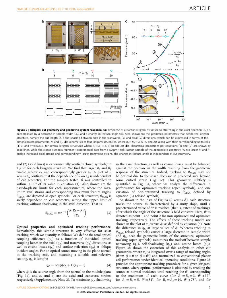
and (2) (solid lines) is experimentally verified (closed symbols) inFig. 2c for each kirigami structure. We find that larger R1 and R2
enable greater eA and correspondingly greater eT. A plot of yversus eA confirms that the dependence of y on eA is independentof cut geometry. For the samples tested, y was controlled towithin ±1.0� of its value in equation (1). Also shown are thepseudo-plastic limits for each superstructure, where the max-imum axial strains and corresponding maximum feature angles,yMAX, are depicted as open symbols. For each structure, yMAX issolely dependent on cut geometry, setting the upper limit oftracking without shadowing in the axial direction. That is:
yMAX ¼ tan� 1 R1R2�R2
2R1
� �ð3Þ
Optical properties and optimized tracking performance.Remarkably, this simple structure is very effective for solartracking, which we quantify as follows. We define the total opticalcoupling efficiency (ZC) as a function of individual opticalcoupling losses in the axial (ZA) and transverse (ZT) directions, aswell as cosine losses (ZO) and surface reflection (ZR) at obliqueincident angles. For an optical source moving in the plane normalto the tracking axis, and assuming a suitable anti-reflectivecoating, ZC is simply:
ZC ¼ cosf eAþ 1ð Þ eTþ 1ð Þ ð4Þ
where f is the source angle from the normal to the module plane(Fig. 1a), and eA and eT are the axial and transverse strains,respectively (Supplementary Note 2). To maximize ZC, shadowing
in the axial direction, as well as cosine losses, must be balancedagainst the decrease in the width resulting from the geometricresponse of the structure. Indeed, tracking to yMAX may notbe optimal due to the sharp decrease in projected area beyondsome critical strain (Fig. 2c). This geometric subtlety isquantified in Fig. 3a, where we analyze the differences inperformance for optimized tracking (open symbols), and onevariation of non-optimized tracking to yMAX defined byequation (3) (closed symbols).
As shown in the inset of Fig. 3a (y versus f), each structuretracks the source as characterized by a unity slope, until apredetermined value of y* is reached (that is, extent of tracking),after which the angle of the structure is held constant. Here, y* isdenoted as point 1 and point 2 for non-optimized and optimizedtracking, respectively. The effects of these tracking modes areshown in the plot of ZC versus f, as defined by equation (4). Notethe difference in ZC at large values of f. Whereas tracking toyMAX (closed symbols) causes a large decrease in sample widthand ZC near the geometric limits of the structure, optimizedtracking (open symbols) minimizes the tradeoff between samplenarrowing (ZT), self-shadowing (ZA) and cosine losses (ZO).Figure 3b shows the extension of this analysis to other cutgeometries, where ZC is integrated over a range of tracking angles(from f¼ 0 to f¼ y*) and normalized to conventional planarcell performance under identical operating conditions. Figure 3bprovides the appropriate tracking procedure for a given kirigamistructure, where optimal performance is obtained by tracking thesource at normal incidence until reaching the y* correspondingto the maximum of each curve (for R1¼R2¼ 3, y*E37�,for R1¼R2¼ 5, y*E54�, for R1¼R2¼ 10, y*E73�, and for
a c
b
L0
Lc
W0W –W0
L –L0
y
R1 = Lc/x
R1 = R2
R1 = R2
R2 = Lc/y
L
x90
60
3 5 10 20
�T =
�A =
201053
30
0
i
i
i
ii
ii
ii
iii
iii
iii
0
–0.2
–0.4
–0.6
–0.8
–1103
Unit cells
10–2 10–1 100 101
Tra
nsve
rse
stra
in �
TF
eatu
re a
ngle
� (
°)
� W0
L0
Axial strain �A
Feature angle
W
Figure 2 | Kirigami cut geometry and geometric system response. (a) Response of a Kapton kirigami structure to stretching in the axial direction (eA) is
accompanied by a decrease in sample width (eT) and a change in feature angle (y). Also shown are the geometric parameters that define the kirigami
structure, namely the cut length (LC) and spacing between cuts in the transverse (x) and axial (y) directions, which can be expressed in terms of the
dimensionless parameters, R1 and R2. (b) Schematics of four kirigami structures, where R1¼ R2¼ 3, 5, 10 and 20, along with their corresponding units cells.
(c) eT and y versus eA for several kirigami structures where R1¼ R2¼ 3, 5, 10 and 20 (b). Theoretical predictions per equations (1) and (2) are shown by
solid lines, while the closed symbols represent experimental data from a 50mm-thick Kapton sample of the appropriate geometry. While larger R1 and R2
enable increased axial strains and correspondingly larger transverse strains, the change in feature angle is independent of cut geometry.
NATURE COMMUNICATIONS | DOI: 10.1038/ncomms9092 ARTICLE
NATURE COMMUNICATIONS | 6:8092 | DOI: 10.1038/ncomms9092 | www.nature.com/naturecommunications 3
& 2015 Macmillan Publishers Limited. All rights reserved.
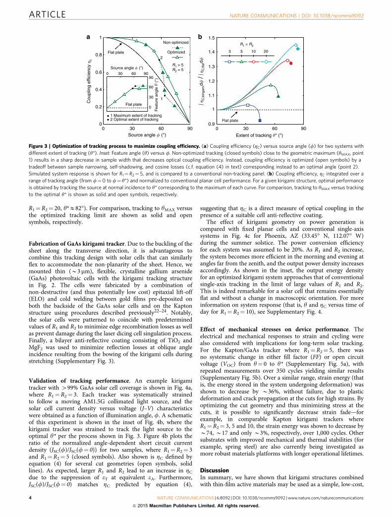
R1¼R2¼ 20, y*E82�). For comparison, tracking to yMAX versusthe optimized tracking limit are shown as solid and opensymbols, respectively.
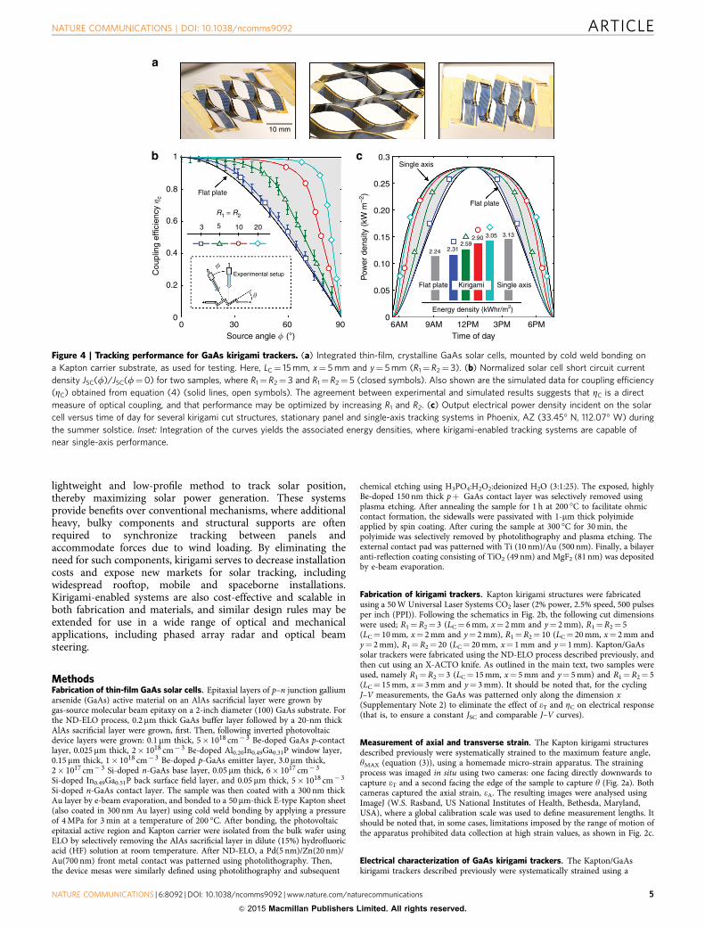
Fabrication of GaAs kirigami tracker. Due to the buckling of thesheet along the transverse direction, it is advantageous tocombine this tracking design with solar cells that can similarlyflex to accommodate the non-planarity of the sheet. Hence, wemounted thin (B3 mm), flexible, crystalline gallium arsenide(GaAs) photovoltaic cells with the kirigami tracking structurein Fig. 2. The cells were fabricated by a combination ofnon-destructive (and thus potentially low cost) epitaxial lift-off(ELO) and cold welding between gold films pre-deposited onboth the backside of the GaAs solar cells and on the Kaptonstructure using procedures described previously22–24. Notably,the solar cells were patterned to coincide with predeterminedvalues of R1 and R2 to minimize edge recombination losses as wellas prevent damage during the laser dicing cell singulation process.Finally, a bilayer anti-reflective coating consisting of TiO2 andMgF2 was used to minimize reflection losses at oblique angleincidence resulting from the bowing of the kirigami cells duringstretching (Supplementary Fig. 3).
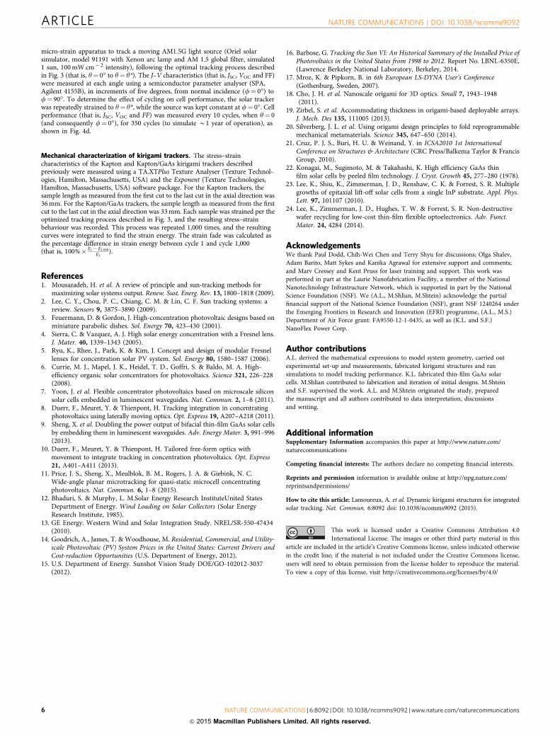
Validation of tracking performance. An example kirigamitracker with 499% GaAs solar cell coverage is shown in Fig. 4a,where R1¼R2¼ 3. Each tracker was systematically strainedto follow a moving AM1.5G collimated light source, and thesolar cell current density versus voltage (J–V) characteristicswere obtained as a function of illumination angle, f. A schematicof this experiment is shown in the inset of Fig. 4b, where thekirigami tracker was strained to track the light source to theoptimal y* per the process shown in Fig. 3. Figure 4b plots theratio of the normalized angle-dependent short circuit currentdensity (JSC(f)/JSC(f¼ 0)) for two samples, where R1¼R2¼ 3and R1¼R2¼ 5 (closed symbols). Also shown is ZC defined byequation (4) for several cut geometries (open symbols, solidlines). As expected, larger R1 and R2 lead to an increase in ZC
due to the suppression of eT at equivalent eA. Furthermore,JSC(f)/JSC(f¼ 0) matches ZC predicted by equation (4),
suggesting that ZC is a direct measure of optical coupling in thepresence of a suitable cell anti-reflective coating.
The effect of kirigami geometry on power generation iscompared with fixed planar cells and conventional single-axissystems in Fig. 4c for Phoenix, AZ (33.45� N, 112.07� W)during the summer solstice. The power conversion efficiencyfor each system was assumed to be 20%. As R1 and R2 increase,the system becomes more efficient in the morning and evening atangles far from the zenith, and the output power density increasesaccordingly. As shown in the inset, the output energy densityfor an optimized kirigami system approaches that of conventionalsingle-axis tracking in the limit of large values of R1 and R2.This is indeed remarkable for a solar cell that remains essentiallyflat and without a change in macroscopic orientation. For moreinformation on system response (that is, y and ZC versus time ofday for R1¼R2¼ 10), see Supplementary Fig. 4.
Effect of mechanical stresses on device performance. Theelectrical and mechanical responses to strain and cycling werealso considered with implications for long-term solar tracking.For the Kapton/GaAs tracker where R1¼R2¼ 5, there wasno systematic change in either fill factor (FF) or open circuitvoltage (VOC) from y¼ 0 to y* (Supplementary Fig. 5a), withrepeated measurements over 350 cycles yielding similar results(Supplementary Fig. 5b). Over a similar range, strain energy (thatis, the energy stored in the system undergoing deformation) wasshown to decrease by B36%, without failure, due to plasticdeformation and crack propagation at the cuts for high strains. Byoptimizing the cut geometry and thus minimizing stress at thecuts, it is possible to significantly decrease strain fade—forexample, in comparable Kapton kirigami trackers whereR1¼R2¼ 3, 5 and 10, the strain energy was shown to decrease byB74, B17 and only B3%, respectively, over 1,000 cycles. Othersubstrates with improved mechanical and thermal stabilities (forexample, spring steel) are also currently being investigated asmore robust materials platforms with longer operational lifetimes.
DiscussionIn summary, we have shown that kirigami structures combinedwith thin-film active materials may be used as a simple, low-cost,
a b1
1
1 Maximum extent of tracking
2
R1 = 5
R1 = R2
R2 = 5
2 Optimal extent of tracking
0.8
1.5
1.4
1.3
1.2
1.1
1
0.90 30
Extent of tracking �* (°)
60 90
0.6
0.4
0.2
00
0
3 5 10 20
0
30
30
60
60
9090
30Source angle � (°)
60 90
Cou
plin
g ef
ficie
ncy
� c
Flat plate
Flat plate
Non-optimized
Source angle � (°)
Fea
ture
ang
le �
(°)
Flat plate
Optimized
∫ �C
,kiri
gam
id�
/ ∫ �
C,fl
atd�
Figure 3 | Optimization of tracking process to maximize coupling efficiency. (a) Coupling efficiency (ZC) versus source angle (f) for two systems with
different extent of tracking (y*). Inset: Feature angle (y) versus f. Non-optimized tracking (closed symbols) close to the geometric maximum (yMAX, point
1) results in a sharp decrease in sample width that decreases optical coupling efficiency. Instead, coupling efficiency is optimized (open symbols) by a
tradeoff between sample narrowing, self-shadowing, and cosine losses (c.f. equation (4) in text) corresponding instead to an optimal angle (point 2).
Simulated system response is shown for R1¼ R2¼ 5, and is compared to a conventional non-tracking panel. (b) Coupling efficiency, ZC integrated over a
range of tracking angle (from f¼0 to f¼ y*) and normalized to conventional planar cell performance. For a given kirigami structure, optimal performance
is obtained by tracking the source at normal incidence to y* corresponding to the maximum of each curve. For comparison, tracking to yMAX versus tracking
to the optimal y* is shown as solid and open symbols, respectively.
ARTICLE NATURE COMMUNICATIONS | DOI: 10.1038/ncomms9092
4 NATURE COMMUNICATIONS | 6:8092 | DOI: 10.1038/ncomms9092 | www.nature.com/naturecommunications
& 2015 Macmillan Publishers Limited. All rights reserved.
lightweight and low-profile method to track solar position,thereby maximizing solar power generation. These systemsprovide benefits over conventional mechanisms, where additionalheavy, bulky components and structural supports are oftenrequired to synchronize tracking between panels andaccommodate forces due to wind loading. By eliminating theneed for such components, kirigami serves to decrease installationcosts and expose new markets for solar tracking, includingwidespread rooftop, mobile and spaceborne installations.Kirigami-enabled systems are also cost-effective and scalable inboth fabrication and materials, and similar design rules may beextended for use in a wide range of optical and mechanicalapplications, including phased array radar and optical beamsteering.
MethodsFabrication of thin-film GaAs solar cells. Epitaxial layers of p–n junction galliumarsenide (GaAs) active material on an AlAs sacrificial layer were grown bygas-source molecular beam epitaxy on a 2-inch diameter (100) GaAs substrate. Forthe ND-ELO process, 0.2 mm thick GaAs buffer layer followed by a 20-nm thickAlAs sacrificial layer were grown, first. Then, following inverted photovoltaicdevice layers were grown: 0.1 mm thick, 5� 1018 cm� 3 Be-doped GaAs p-contactlayer, 0.025 mm thick, 2� 1018 cm� 3 Be-doped Al0.20In0.49Ga0.31P window layer,0.15 mm thick, 1� 1018 cm� 3 Be-doped p-GaAs emitter layer, 3.0 mm thick,2� 1017 cm� 3 Si-doped n-GaAs base layer, 0.05 mm thick, 6� 1017 cm� 3
Si-doped In0.49Ga0.51P back surface field layer, and 0.05 mm thick, 5� 1018 cm� 3
Si-doped n-GaAs contact layer. The sample was then coated with a 300 nm thickAu layer by e-beam evaporation, and bonded to a 50 mm-thick E-type Kapton sheet(also coated in 300 nm Au layer) using cold weld bonding by applying a pressureof 4 MPa for 3 min at a temperature of 200 �C. After bonding, the photovoltaicepitaxial active region and Kapton carrier were isolated from the bulk wafer usingELO by selectively removing the AlAs sacrificial layer in dilute (15%) hydrofluoricacid (HF) solution at room temperature. After ND-ELO, a Pd(5 nm)/Zn(20 nm)/Au(700 nm) front metal contact was patterned using photolithography. Then,the device mesas were similarly defined using photolithography and subsequent
chemical etching using H3PO4:H2O2:deionized H2O (3:1:25). The exposed, highlyBe-doped 150 nm thick pþ GaAs contact layer was selectively removed usingplasma etching. After annealing the sample for 1 h at 200 �C to facilitate ohmiccontact formation, the sidewalls were passivated with 1-mm thick polyimideapplied by spin coating. After curing the sample at 300 �C for 30 min, thepolyimide was selectively removed by photolithography and plasma etching. Theexternal contact pad was patterned with Ti (10 nm)/Au (500 nm). Finally, a bilayeranti-reflection coating consisting of TiO2 (49 nm) and MgF2 (81 nm) was depositedby e-beam evaporation.
Fabrication of kirigami trackers. Kapton kirigami structures were fabricatedusing a 50 W Universal Laser Systems CO2 laser (2% power, 2.5% speed, 500 pulsesper inch (PPI)). Following the schematics in Fig. 2b, the following cut dimensionswere used; R1¼R2¼ 3 (LC¼ 6 mm, x¼ 2 mm and y¼ 2 mm), R1¼R2¼ 5(LC¼ 10 mm, x¼ 2 mm and y¼ 2 mm), R1¼R2¼ 10 (LC¼ 20 mm, x¼ 2 mm andy¼ 2 mm), R1¼R2¼ 20 (LC¼ 20 mm, x¼ 1 mm and y¼ 1 mm). Kapton/GaAssolar trackers were fabricated using the ND-ELO process described previously, andthen cut using an X-ACTO knife. As outlined in the main text, two samples wereused, namely R1¼R2¼ 3 (LC¼ 15 mm, x¼ 5 mm and y¼ 5 mm) and R1¼R2¼ 5(LC¼ 15 mm, x¼ 3 mm and y¼ 3 mm). It should be noted that, for the cyclingJ–V measurements, the GaAs was patterned only along the dimension x(Supplementary Note 2) to eliminate the effect of eT and ZC on electrical response(that is, to ensure a constant JSC and comparable J–V curves).
Measurement of axial and transverse strain. The Kapton kirigami structuresdescribed previously were systematically strained to the maximum feature angle,yMAX (equation (3)), using a homemade micro-strain apparatus. The strainingprocess was imaged in situ using two cameras: one facing directly downwards tocapture eT and a second facing the edge of the sample to capture y (Fig. 2a). Bothcameras captured the axial strain, eA. The resulting images were analysed usingImageJ (W.S. Rasband, US National Institutes of Health, Bethesda, Maryland,USA), where a global calibration scale was used to define measurement lengths. Itshould be noted that, in some cases, limitations imposed by the range of motion ofthe apparatus prohibited data collection at high strain values, as shown in Fig. 2c.
Electrical characterization of GaAs kirigami trackers. The Kapton/GaAskirigami trackers described previously were systematically strained using a
10 mm
Flat plate
Flat plate
Flat plate Kirigami Single axis
Energy density (kWhr/m2)
2.24 2.312.59
2.90 3.05 3.13
Single axis
R1 = R2
3
1
5 10 20
0.8
0.6
0.4
0.2
00 30 60
0
0.05
0.10
Pow
er d
ensi
ty (
kW m
–2)
0.15
0.20
0.25
0.3
90 6AM 9AM 12PM 3PM 6PMSource angle � (°) Time of day
Cou
plin
g ef
ficie
ncy
� c
�Experimental setup
�
Figure 4 | Tracking performance for GaAs kirigami trackers. (a) Integrated thin-film, crystalline GaAs solar cells, mounted by cold weld bonding on
a Kapton carrier substrate, as used for testing. Here, LC¼ 15 mm, x¼ 5 mm and y¼ 5 mm (R1¼ R2¼ 3). (b) Normalized solar cell short circuit current
density JSC(f)/JSC(f¼0) for two samples, where R1¼ R2¼ 3 and R1¼ R2¼ 5 (closed symbols). Also shown are the simulated data for coupling efficiency
(ZC) obtained from equation (4) (solid lines, open symbols). The agreement between experimental and simulated results suggests that ZC is a direct
measure of optical coupling, and that performance may be optimized by increasing R1 and R2. (c) Output electrical power density incident on the solar
cell versus time of day for several kirigami cut structures, stationary panel and single-axis tracking systems in Phoenix, AZ (33.45� N, 112.07� W) during
the summer solstice. Inset: Integration of the curves yields the associated energy densities, where kirigami-enabled tracking systems are capable of
near single-axis performance.
NATURE COMMUNICATIONS | DOI: 10.1038/ncomms9092 ARTICLE
NATURE COMMUNICATIONS | 6:8092 | DOI: 10.1038/ncomms9092 | www.nature.com/naturecommunications 5
& 2015 Macmillan Publishers Limited. All rights reserved.
micro-strain apparatus to track a moving AM1.5G light source (Oriel solarsimulator, model 91191 with Xenon arc lamp and AM 1.5 global filter, simulated1 sun, 100 mW cm� 2 intensity), following the optimal tracking process describedin Fig. 3 (that is, y¼ 0� to y¼ y*). The J–V characteristics (that is, JSC, VOC and FF)were measured at each angle using a semiconductor parameter analyser (SPA,Agilent 4155B), in increments of five degrees, from normal incidence (f¼ 0�) tof¼ 90�. To determine the effect of cycling on cell performance, the solar trackerwas repeatedly strained to y¼ y*, while the source was kept constant at f¼ 0�. Cellperformance (that is, JSC, VOC and FF) was measured every 10 cycles, when y¼ 0(and consequently f¼ 0�), for 350 cycles (to simulate B1 year of operation), asshown in Fig. 4d.
Mechanical characterization of kirigami trackers. The stress–straincharacteristics of the Kapton and Kapton/GaAs kirigami trackers describedpreviously were measured using a TA.XTPlus Texture Analyser (Texture Technol-ogies, Hamilton, Massachusetts, USA) and the Exponent (Texture Technologies,Hamilton, Massachusetts, USA) software package. For the Kapton trackers, thesample length as measured from the first cut to the last cut in the axial direction was36 mm. For the Kapton/GaAs trackers, the sample length as measured from the firstcut to the last cut in the axial direction was 33 mm. Each sample was strained per theoptimized tracking process described in Fig. 3, and the resulting stress–strainbehaviour was recorded. This process was repeated 1,000 times, and the resultingcurves were integrated to find the strain energy. The strain fade was calculated asthe percentage difference in strain energy between cycle 1 and cycle 1,000(that is, 100%� E1 � E1;000
E1).
References1. Mousazadeh, H. et al. A review of principle and sun-tracking methods for
maximizing solar systems output. Renew. Sust. Energ. Rev. 13, 1800–1818 (2009).2. Lee, C. Y., Chou, P. C., Chiang, C. M. & Lin, C. F. Sun tracking systems: a
review. Sensors 9, 3875–3890 (2009).3. Feuermann, D. & Gordon, J. High-concentration photovoltaic designs based on
miniature parabolic dishes. Sol. Energy 70, 423–430 (2001).4. Sierra, C. & Vazquez, A. J. High solar energy concentration with a Fresnel lens.
J. Mater. 40, 1339–1343 (2005).5. Ryu, K., Rhee, J., Park, K. & Kim, J. Concept and design of modular Fresnel
lenses for concentration solar PV system. Sol. Energy 80, 1580–1587 (2006).6. Currie, M. J., Mapel, J. K., Heidel, T. D., Goffri, S. & Baldo, M. A. High-
efficiency organic solar concentrators for photovoltaics. Science 321, 226–228(2008).
7. Yoon, J. et al. Flexible concentrator photovoltaics based on microscale siliconsolar cells embedded in luminescent waveguides. Nat. Commun. 2, 1–8 (2011).
8. Duerr, F., Meuret, Y. & Thienpont, H. Tracking integration in concentratingphotovoltaics using laterally moving optics. Opt. Express 19, A207–A218 (2011).
9. Sheng, X. et al. Doubling the power output of bifacial thin-film GaAs solar cellsby embedding them in luminescent waveguides. Adv. Energy Mater. 3, 991–996(2013).
10. Duerr, F., Meuret, Y. & Thienpont, H. Tailored free-form optics withmovement to integrate tracking in concentration photovoltaics. Opt. Express21, A401–A411 (2013).
11. Price, J. S., Sheng, X., Meulblok, B. M., Rogers, J. A. & Giebink, N. C.Wide-angle planar microtracking for quasi-static microcell concentratingphotovoltaics. Nat. Commun. 6, 1–8 (2015).
12. Bhaduri, S. & Murphy, L. M.Solar Energy Research InstituteUnited StatesDepartment of Energy. Wind Loading on Solar Collectors (Solar EnergyResearch Institute, 1985).
13. GE Energy. Western Wind and Solar Integration Study. NREL/SR-550-47434(2010).
14. Goodrich, A., James, T. & Woodhouse, M. Residential, Commercial, and Utility-scale Photovoltaic (PV) System Prices in the United States: Current Drivers andCost-reduction Opportunities (U.S. Department of Energy, 2012).
15. U.S. Department of Energy. Sunshot Vision Study DOE/GO-102012-3037(2012).
16. Barbose, G. Tracking the Sun VI: An Historical Summary of the Installed Price ofPhotovoltaics in the United States from 1998 to 2012. Report No. LBNL-6350E,(Lawrence Berkeley National Laboratory, Berkeley, 2014.
17. Mroz, K. & Pipkorn, B. in 6th European LS-DYNA User’s Conference(Gothenburg, Sweden, 2007).
18. Cho, J. H. et al. Nanoscale origami for 3D optics. Small 7, 1943–1948(2011).
19. Zirbel, S. et al. Accommodating thickness in origami-based deployable arrays.J. Mech. Des 135, 111005 (2013).
20. Silverberg, J. L. et al. Using origami design principles to fold reprogrammablemechanical metamaterials. Science 345, 647–650 (2014).
21. Cruz, P. J. S., Buri, H. U. & Weinand, Y. in ICSA2010 1st InternationalConference on Structures & Architecture (CRC Press/Balkema Taylor & FrancisGroup, 2010).
22. Konagai, M., Sugimoto, M. & Takahashi, K. High efficiency GaAs thinfilm solar cells by peeled film technology. J. Cryst. Growth 45, 277–280 (1978).
23. Lee, K., Shiu, K., Zimmerman, J. D., Renshaw, C. K. & Forrest, S. R. Multiplegrowths of epitaxial lift-off solar cells from a single InP substrate. Appl. Phys.Lett. 97, 101107 (2010).
24. Lee, K., Zimmerman, J. D., Hughes, T. W. & Forrest, S. R. Non-destructivewafer recycling for low-cost thin-film flexible optoelectronics. Adv. Funct.Mater. 24, 4284 (2014).
AcknowledgementsWe thank Paul Dodd, Chih-Wei Chen and Terry Shyu for discussions; Olga Shalev,Adam Barito, Matt Sykes and Kanika Agrawal for extensive support and comments;and Marv Cressey and Kent Pruss for laser training and support. This work wasperformed in part at the Laurie Nanofabrication Facility, a member of the NationalNanotechnology Infrastructure Network, which is supported in part by the NationalScience Foundation (NSF). We (A.L., M.Shlian, M.Shtein) acknowledge the partialfinancial support of the National Science Foundation (NSF), grant NSF 1240264 underthe Emerging Frontiers in Research and Innovation (EFRI) programme, (A.L., M.S.)Department of Air Force grant: FA9550-12-1-0435, as well as (K.L. and S.F.)NanoFlex Power Corp.
Author contributionsA.L. derived the mathematical expressions to model system geometry, carried outexperimental set-up and measurements, fabricated kirigami structures and ransimulations to model tracking performance. K.L. fabricated thin-film GaAs solarcells. M.Shlian contributed to fabrication and iteration of initial designs. M.Shteinand S.F. supervised the work. A.L. and M.Shtein originated the study, preparedthe manuscript and all authors contributed to data interpretation, discussionsand writing.
Additional informationSupplementary Information accompanies this paper at http://www.nature.com/naturecommunications
Competing financial interests: The authors declare no competing financial interests.
Reprints and permission information is available online at http://npg.nature.com/reprintsandpermissions/
How to cite this article: Lamoureux, A. et al. Dynamic kirigami structures for integratedsolar tracking. Nat. Commun. 6:8092 doi: 10.1038/ncomms9092 (2015).
This work is licensed under a Creative Commons Attribution 4.0International License. The images or other third party material in this
article are included in the article’s Creative Commons license, unless indicated otherwisein the credit line; if the material is not included under the Creative Commons license,users will need to obtain permission from the license holder to reproduce the material.To view a copy of this license, visit http://creativecommons.org/licenses/by/4.0/
ARTICLE NATURE COMMUNICATIONS | DOI: 10.1038/ncomms9092
6 NATURE COMMUNICATIONS | 6:8092 | DOI: 10.1038/ncomms9092 | www.nature.com/naturecommunications
& 2015 Macmillan Publishers Limited. All rights reserved.