dynamic nfc/rfid tag ic with 4-kbit, 16-kbit or 64-kbit ... · dynamic nfc/rfid tag ic with 4-kbit,...
TRANSCRIPT
This is information on a product in full production.
December 2017 DocID027603 Rev 4 1/220
ST25DV04K ST25DV16K ST25DV64K
Dynamic NFC/RFID tag IC with 4-Kbit, 16-Kbit or 64-Kbit EEPROM, and fast transfer mode capability
Datasheet - production data
FeaturesI2C interface• Two-wire I2C serial interface supports 1MHz
protocol• Single supply voltage: 1.8V to 5.5V• Multiple byte write programing (up to 256 bytes)
Contactless interface• Based on ISO/IEC 15693• NFC Forum Type 5 tag certified by the NFC Forum• Supports all ISO/IEC 15693 modulations, coding,
subcarrier modes and data rates• Custom Fast read access up to 53 Kbit/s• Single and multiple blocks read (same for Extended
commands)• Single and multiple blocks write (up to 4) (same for
Extended commands)• Internal tuning capacitance: 28.5 pF
Memory• Up to 64-kbits of EEPROM (depending on version)• I2C interface accesses bytes• RF interface accesses blocks of 4 bytes• Write time:
– From I2C: typical 5ms for 1 byte– From RF: typical 5ms for 1 block
• Data retention: 40 years• Write cycles endurance:
– 1 million write cycles at 25 °C– 600k write cycles at 85 °C– 500k write cycles at 105 °C– 400k write cycles at 125 °C
Fast transfer mode• Fast data transfer between I2C and RF interfaces• Half-duplex 256-byte dedicated buffer
Energy harvesting• Analog output pin to power external components
Data protection• User memory: 1 to 4 configurable areas, protectable
in read and/or write by three 64-bit passwords in RF and one 64-bit password in I2C
• System configuration: protected in write by a 64-bit password in RF and a 64-bit password in I2C
GPO• Interruption pin configurable on multiple RF events
(field change, memory write, activity, Fast Transfer end, user set/reset/pulse)
• Open Drain or CMOS output (depending on version)
Low power mode (10-ball and 12-pin package only)• Input pin to trigger low power mode
RF management• RF command interpreter enabled/disabled from I2C
host controller
Temperature range• Range 6:
– From -40 to 85 °C• Range 8:
– From -40 to 105 °C (UDFPN8 and UDFPN12 only)
– From -40 to 125 °C (SO8N and TSSOP8 only, 105 °C max on RF interface)
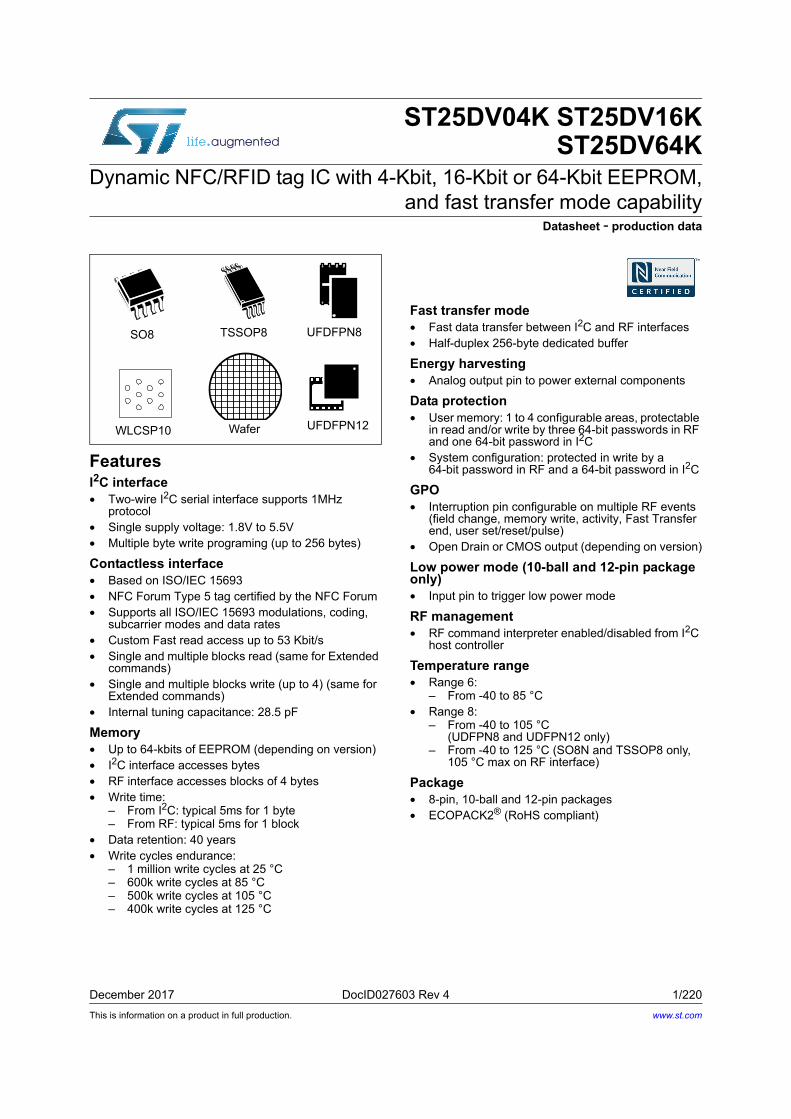
Package• 8-pin, 10-ball and 12-pin packages• ECOPACK2® (RoHS compliant)
SO8 TSSOP8
UFDFPN12
UFDFPN8
WaferWLCSP10
www.st.com

Contents ST25DV04K ST25DV16K ST25DV64K
2/220 DocID027603 Rev 4
Contents
1 Description . . . . . . . . . . . . . . . . . . . . . . . . . . . . . . . . . . . . . . . . . . . . . . . . 17
1.1 ST25DVxxx block diagram . . . . . . . . . . . . . . . . . . . . . . . . . . . . . . . . . . . . 17
1.2 ST25DVxxx packaging . . . . . . . . . . . . . . . . . . . . . . . . . . . . . . . . . . . . . . . 18
2 Signal descriptions . . . . . . . . . . . . . . . . . . . . . . . . . . . . . . . . . . . . . . . . . 20
2.1 Serial link (SCL, SDA) . . . . . . . . . . . . . . . . . . . . . . . . . . . . . . . . . . . . . . . 20
2.1.1 Serial clock (SCL) . . . . . . . . . . . . . . . . . . . . . . . . . . . . . . . . . . . . . . . . . 20
2.1.2 Serial data (SDA) . . . . . . . . . . . . . . . . . . . . . . . . . . . . . . . . . . . . . . . . . . 20
2.2 Power control (VCC, LPD,VSS) . . . . . . . . . . . . . . . . . . . . . . . . . . . . . . . . . 20
2.2.1 Supply voltage (VCC) . . . . . . . . . . . . . . . . . . . . . . . . . . . . . . . . . . . . . . . 20
2.2.2 Low Power Down (LPD) . . . . . . . . . . . . . . . . . . . . . . . . . . . . . . . . . . . . 20
2.2.3 Ground (VSS) . . . . . . . . . . . . . . . . . . . . . . . . . . . . . . . . . . . . . . . . . . . . . 20
2.3 RF link (AC0 AC1) . . . . . . . . . . . . . . . . . . . . . . . . . . . . . . . . . . . . . . . . . . 21
2.3.1 Antenna coil (AC0, AC1) . . . . . . . . . . . . . . . . . . . . . . . . . . . . . . . . . . . . 21
2.4 Process control (VDCG, GPO) . . . . . . . . . . . . . . . . . . . . . . . . . . . . . . . . . . 21
2.4.1 Driver Supply voltage (VDCG) . . . . . . . . . . . . . . . . . . . . . . . . . . . . . . . . 21
2.4.2 General purpose output (GPO) . . . . . . . . . . . . . . . . . . . . . . . . . . . . . . . 21
2.5 Energy harvesting analog output (V_EH) . . . . . . . . . . . . . . . . . . . . . . . . . 21
3 Power management . . . . . . . . . . . . . . . . . . . . . . . . . . . . . . . . . . . . . . . . 22
3.1 Wired interface . . . . . . . . . . . . . . . . . . . . . . . . . . . . . . . . . . . . . . . . . . . . . 22
3.2 Contactless interface . . . . . . . . . . . . . . . . . . . . . . . . . . . . . . . . . . . . . . . . 23
4 Memory management . . . . . . . . . . . . . . . . . . . . . . . . . . . . . . . . . . . . . . . 24
4.1 Memory organization overview . . . . . . . . . . . . . . . . . . . . . . . . . . . . . . . . . 24
4.2 User memory . . . . . . . . . . . . . . . . . . . . . . . . . . . . . . . . . . . . . . . . . . . . . . 25
4.2.1 User memory areas . . . . . . . . . . . . . . . . . . . . . . . . . . . . . . . . . . . . . . . . 27
4.3 System configuration area . . . . . . . . . . . . . . . . . . . . . . . . . . . . . . . . . . . . 31
4.4 Dynamic configuration . . . . . . . . . . . . . . . . . . . . . . . . . . . . . . . . . . . . . . . 34
4.5 Fast transfer mode mailbox . . . . . . . . . . . . . . . . . . . . . . . . . . . . . . . . . . . 35
5 ST25DVxxx specific features . . . . . . . . . . . . . . . . . . . . . . . . . . . . . . . . . 36
5.1 Fast transfer mode (FTM) . . . . . . . . . . . . . . . . . . . . . . . . . . . . . . . . . . . . 37
DocID027603 Rev 4 3/220
ST25DV04K ST25DV16K ST25DV64K Contents
7
5.1.1 Fast transfer mode registers . . . . . . . . . . . . . . . . . . . . . . . . . . . . . . . . . 37
5.1.2 Fast transfer mode usage . . . . . . . . . . . . . . . . . . . . . . . . . . . . . . . . . . . 39
5.2 GPO . . . . . . . . . . . . . . . . . . . . . . . . . . . . . . . . . . . . . . . . . . . . . . . . . . . . . 44
5.2.1 ST25DVxxx interrupt capabilities on RF events . . . . . . . . . . . . . . . . . . . 44
5.2.2 GPO and power supply . . . . . . . . . . . . . . . . . . . . . . . . . . . . . . . . . . . . . 52
5.2.3 GPO registers . . . . . . . . . . . . . . . . . . . . . . . . . . . . . . . . . . . . . . . . . . . . 53
5.2.4 Configuring GPO . . . . . . . . . . . . . . . . . . . . . . . . . . . . . . . . . . . . . . . . . . 57
5.3 Energy Harvesting (EH) . . . . . . . . . . . . . . . . . . . . . . . . . . . . . . . . . . . . . . 59
5.3.1 Energy harvesting registers . . . . . . . . . . . . . . . . . . . . . . . . . . . . . . . . . . 59
5.3.2 Energy harvesting feature description . . . . . . . . . . . . . . . . . . . . . . . . . . 60
5.3.3 EH delivery state diagram . . . . . . . . . . . . . . . . . . . . . . . . . . . . . . . . . . . 61
5.3.4 EH delivery sequence . . . . . . . . . . . . . . . . . . . . . . . . . . . . . . . . . . . . . . 62
5.4 RF management feature . . . . . . . . . . . . . . . . . . . . . . . . . . . . . . . . . . . . . 63
5.4.1 RF management registers . . . . . . . . . . . . . . . . . . . . . . . . . . . . . . . . . . . 63
5.4.2 RF management feature description . . . . . . . . . . . . . . . . . . . . . . . . . . . 63
5.5 Interface Arbitration . . . . . . . . . . . . . . . . . . . . . . . . . . . . . . . . . . . . . . . . . 65
5.6 Data Protection . . . . . . . . . . . . . . . . . . . . . . . . . . . . . . . . . . . . . . . . . . . . . 66
5.6.1 Data protection registers . . . . . . . . . . . . . . . . . . . . . . . . . . . . . . . . . . . . 66
5.6.2 Passwords and security sessions . . . . . . . . . . . . . . . . . . . . . . . . . . . . . 75
5.6.3 User memory protection . . . . . . . . . . . . . . . . . . . . . . . . . . . . . . . . . . . . 78
5.6.4 System memory protection . . . . . . . . . . . . . . . . . . . . . . . . . . . . . . . . . . 80
5.7 Device Parameter Registers . . . . . . . . . . . . . . . . . . . . . . . . . . . . . . . . . . 81
6 I2C operation . . . . . . . . . . . . . . . . . . . . . . . . . . . . . . . . . . . . . . . . . . . . . . 86
6.1 I2C protocol . . . . . . . . . . . . . . . . . . . . . . . . . . . . . . . . . . . . . . . . . . . . . . . 86
6.1.1 Start condition . . . . . . . . . . . . . . . . . . . . . . . . . . . . . . . . . . . . . . . . . . . . 86
6.1.2 Stop condition . . . . . . . . . . . . . . . . . . . . . . . . . . . . . . . . . . . . . . . . . . . . 87
6.1.3 Acknowledge bit (ACK) . . . . . . . . . . . . . . . . . . . . . . . . . . . . . . . . . . . . . 87
6.1.4 Data input . . . . . . . . . . . . . . . . . . . . . . . . . . . . . . . . . . . . . . . . . . . . . . . 87
6.2 I2C timeout . . . . . . . . . . . . . . . . . . . . . . . . . . . . . . . . . . . . . . . . . . . . . . . . 87
6.2.1 I2C timeout on Start condition . . . . . . . . . . . . . . . . . . . . . . . . . . . . . . . . 87
6.2.2 I2C timeout on clock period . . . . . . . . . . . . . . . . . . . . . . . . . . . . . . . . . . 88
6.3 Device addressing . . . . . . . . . . . . . . . . . . . . . . . . . . . . . . . . . . . . . . . . . . 88
6.4 I2C Write operations . . . . . . . . . . . . . . . . . . . . . . . . . . . . . . . . . . . . . . . . . 89
6.4.1 I2C Byte write . . . . . . . . . . . . . . . . . . . . . . . . . . . . . . . . . . . . . . . . . . . . . 90
6.4.2 I2C Sequential write . . . . . . . . . . . . . . . . . . . . . . . . . . . . . . . . . . . . . . . . 90
Contents ST25DV04K ST25DV16K ST25DV64K
4/220 DocID027603 Rev 4
6.4.3 Minimizing system delays by polling on ACK . . . . . . . . . . . . . . . . . . . . 92
6.5 I2C read operations . . . . . . . . . . . . . . . . . . . . . . . . . . . . . . . . . . . . . . . . . 94
6.5.1 Random Address Read . . . . . . . . . . . . . . . . . . . . . . . . . . . . . . . . . . . . . 94
6.5.2 Current Address Read . . . . . . . . . . . . . . . . . . . . . . . . . . . . . . . . . . . . . . 94
6.5.3 Sequential Read access . . . . . . . . . . . . . . . . . . . . . . . . . . . . . . . . . . . . 95
6.5.4 Acknowledge in Read mode . . . . . . . . . . . . . . . . . . . . . . . . . . . . . . . . . 96
6.6 I2C password management . . . . . . . . . . . . . . . . . . . . . . . . . . . . . . . . . . . 97
6.6.1 I2C present password command description . . . . . . . . . . . . . . . . . . . . . 97
6.6.2 I2C write password command description . . . . . . . . . . . . . . . . . . . . . . . 98
7 RF operations . . . . . . . . . . . . . . . . . . . . . . . . . . . . . . . . . . . . . . . . . . . . . 99
7.1 RF communication . . . . . . . . . . . . . . . . . . . . . . . . . . . . . . . . . . . . . . . . . . 99
7.1.1 Access to a ISO/IEC 15693 device . . . . . . . . . . . . . . . . . . . . . . . . . . . . 99
7.2 RF communication and energy harvesting . . . . . . . . . . . . . . . . . . . . . . . 100
7.3 Fast transfer mode mailbox access in RF . . . . . . . . . . . . . . . . . . . . . . . 100
7.4 RF protocol description . . . . . . . . . . . . . . . . . . . . . . . . . . . . . . . . . . . . . 100
7.4.1 Protocol description . . . . . . . . . . . . . . . . . . . . . . . . . . . . . . . . . . . . . . . 100
7.4.2 ST25DVxxx states referring to RF protocol . . . . . . . . . . . . . . . . . . . . . 101
7.4.3 Modes . . . . . . . . . . . . . . . . . . . . . . . . . . . . . . . . . . . . . . . . . . . . . . . . . 103
7.4.4 Request format . . . . . . . . . . . . . . . . . . . . . . . . . . . . . . . . . . . . . . . . . . 103
7.4.5 Request flags . . . . . . . . . . . . . . . . . . . . . . . . . . . . . . . . . . . . . . . . . . . . 103
7.4.6 Response format . . . . . . . . . . . . . . . . . . . . . . . . . . . . . . . . . . . . . . . . . 105
7.4.7 Response flags . . . . . . . . . . . . . . . . . . . . . . . . . . . . . . . . . . . . . . . . . . 105
7.4.8 Response and error code . . . . . . . . . . . . . . . . . . . . . . . . . . . . . . . . . . 106
7.5 Timing definition . . . . . . . . . . . . . . . . . . . . . . . . . . . . . . . . . . . . . . . . . . . 106
7.6 RF Commands . . . . . . . . . . . . . . . . . . . . . . . . . . . . . . . . . . . . . . . . . . . . 108
7.6.1 RF command code list . . . . . . . . . . . . . . . . . . . . . . . . . . . . . . . . . . . . . 108
7.6.2 Command codes list . . . . . . . . . . . . . . . . . . . . . . . . . . . . . . . . . . . . . . 110
7.6.3 General Command Rules . . . . . . . . . . . . . . . . . . . . . . . . . . . . . . . . . . 111
7.6.4 Inventory . . . . . . . . . . . . . . . . . . . . . . . . . . . . . . . . . . . . . . . . . . . . . . . 111
7.6.5 Stay Quiet . . . . . . . . . . . . . . . . . . . . . . . . . . . . . . . . . . . . . . . . . . . . . . 112
7.6.6 Read Single Block . . . . . . . . . . . . . . . . . . . . . . . . . . . . . . . . . . . . . . . . 113
7.6.7 Extended Read Single Block . . . . . . . . . . . . . . . . . . . . . . . . . . . . . . . . 114
7.6.8 Write Single Block . . . . . . . . . . . . . . . . . . . . . . . . . . . . . . . . . . . . . . . . 115
7.6.9 Extended Write Single Block . . . . . . . . . . . . . . . . . . . . . . . . . . . . . . . . 117
7.6.10 Lock block . . . . . . . . . . . . . . . . . . . . . . . . . . . . . . . . . . . . . . . . . . . . . . 118

DocID027603 Rev 4 5/220
ST25DV04K ST25DV16K ST25DV64K Contents
7
7.6.11 Extended Lock block . . . . . . . . . . . . . . . . . . . . . . . . . . . . . . . . . . . . . . 120
7.6.12 Read Multiple Blocks . . . . . . . . . . . . . . . . . . . . . . . . . . . . . . . . . . . . . . 121
7.6.13 Extended Read Multiple Blocks . . . . . . . . . . . . . . . . . . . . . . . . . . . . . . 122
7.6.14 Write Multiple Blocks . . . . . . . . . . . . . . . . . . . . . . . . . . . . . . . . . . . . . . 124
7.6.15 Extended Write Multiple Blocks . . . . . . . . . . . . . . . . . . . . . . . . . . . . . . 126
7.6.16 Select . . . . . . . . . . . . . . . . . . . . . . . . . . . . . . . . . . . . . . . . . . . . . . . . . . 127
7.6.17 Reset to Ready . . . . . . . . . . . . . . . . . . . . . . . . . . . . . . . . . . . . . . . . . . 128
7.6.18 Write AFI . . . . . . . . . . . . . . . . . . . . . . . . . . . . . . . . . . . . . . . . . . . . . . . 129
7.6.19 Lock AFI . . . . . . . . . . . . . . . . . . . . . . . . . . . . . . . . . . . . . . . . . . . . . . . . 131
7.6.20 Write DSFID . . . . . . . . . . . . . . . . . . . . . . . . . . . . . . . . . . . . . . . . . . . . . 132
7.6.21 Lock DSFID . . . . . . . . . . . . . . . . . . . . . . . . . . . . . . . . . . . . . . . . . . . . . 133
7.6.22 Get System Info . . . . . . . . . . . . . . . . . . . . . . . . . . . . . . . . . . . . . . . . . . 134
7.6.23 Extended Get System Info . . . . . . . . . . . . . . . . . . . . . . . . . . . . . . . . . . 136
7.6.24 Get Multiple Block Security Status . . . . . . . . . . . . . . . . . . . . . . . . . . . . 140
7.6.25 Extended Get Multiple Block Security Status . . . . . . . . . . . . . . . . . . . . 142
7.6.26 Read Configuration . . . . . . . . . . . . . . . . . . . . . . . . . . . . . . . . . . . . . . . 143
7.6.27 Write Configuration . . . . . . . . . . . . . . . . . . . . . . . . . . . . . . . . . . . . . . . 144
7.6.28 Read Dynamic Configuration . . . . . . . . . . . . . . . . . . . . . . . . . . . . . . . . 146
7.6.29 Write Dynamic Configuration . . . . . . . . . . . . . . . . . . . . . . . . . . . . . . . . 147
7.6.30 Manage GPO . . . . . . . . . . . . . . . . . . . . . . . . . . . . . . . . . . . . . . . . . . . . 148
7.6.31 Write Message . . . . . . . . . . . . . . . . . . . . . . . . . . . . . . . . . . . . . . . . . . . 150
7.6.32 Read Message Length . . . . . . . . . . . . . . . . . . . . . . . . . . . . . . . . . . . . . 151
7.6.33 Read Message . . . . . . . . . . . . . . . . . . . . . . . . . . . . . . . . . . . . . . . . . . . 152
7.6.34 Fast Read Message . . . . . . . . . . . . . . . . . . . . . . . . . . . . . . . . . . . . . . . 153
7.6.35 Write Password . . . . . . . . . . . . . . . . . . . . . . . . . . . . . . . . . . . . . . . . . . 154
7.6.36 Present Password . . . . . . . . . . . . . . . . . . . . . . . . . . . . . . . . . . . . . . . . 156
7.6.37 Fast Read Single Block . . . . . . . . . . . . . . . . . . . . . . . . . . . . . . . . . . . . 157
7.6.38 Fast Extended Read Single Block . . . . . . . . . . . . . . . . . . . . . . . . . . . . 159
7.6.39 Fast Read Multiple Blocks . . . . . . . . . . . . . . . . . . . . . . . . . . . . . . . . . . 160
7.6.40 Fast Extended Read Multiple Block . . . . . . . . . . . . . . . . . . . . . . . . . . . 162
7.6.41 Fast Write Message . . . . . . . . . . . . . . . . . . . . . . . . . . . . . . . . . . . . . . . 164
7.6.42 Fast Read Message Length . . . . . . . . . . . . . . . . . . . . . . . . . . . . . . . . . 165
7.6.43 Fast Read Dynamic Configuration . . . . . . . . . . . . . . . . . . . . . . . . . . . . 166
7.6.44 Fast Write Dynamic Configuration . . . . . . . . . . . . . . . . . . . . . . . . . . . . 167
8 Unique identifier (UID) . . . . . . . . . . . . . . . . . . . . . . . . . . . . . . . . . . . . . 169

Contents ST25DV04K ST25DV16K ST25DV64K
6/220 DocID027603 Rev 4
9 Device parameters . . . . . . . . . . . . . . . . . . . . . . . . . . . . . . . . . . . . . . . . 170
9.1 Maximum rating . . . . . . . . . . . . . . . . . . . . . . . . . . . . . . . . . . . . . . . . . . . 170
9.2 I2C DC and AC parameters . . . . . . . . . . . . . . . . . . . . . . . . . . . . . . . . . . 171
9.3 GPO Characteristics . . . . . . . . . . . . . . . . . . . . . . . . . . . . . . . . . . . . . . . . 179
9.4 RF electrical parameters . . . . . . . . . . . . . . . . . . . . . . . . . . . . . . . . . . . . 180
10 Package information . . . . . . . . . . . . . . . . . . . . . . . . . . . . . . . . . . . . . . . 183
10.1 SO8N package information . . . . . . . . . . . . . . . . . . . . . . . . . . . . . . . . . . 183
10.2 TSSOP8 package information . . . . . . . . . . . . . . . . . . . . . . . . . . . . . . . . 184
10.3 UFDFN8 package information . . . . . . . . . . . . . . . . . . . . . . . . . . . . . . . . 186
10.4 UFDFPN12 package information . . . . . . . . . . . . . . . . . . . . . . . . . . . . . . 188
10.5 WLCSP10 package information . . . . . . . . . . . . . . . . . . . . . . . . . . . . . . . 189
11 Ordering information . . . . . . . . . . . . . . . . . . . . . . . . . . . . . . . . . . . . . . 191
Appendix A Bit representation and coding for fast commands. . . . . . . . . . . . . . . . . . . . . . . . . . . . . . . . . . . . . . 193
A.1 Bit coding using one subcarrier . . . . . . . . . . . . . . . . . . . . . . . . . . . . . . . . 193
A.1.1 High data rate . . . . . . . . . . . . . . . . . . . . . . . . . . . . . . . . . . . . . . . . . . . . 193
A.1.2 Low data rate . . . . . . . . . . . . . . . . . . . . . . . . . . . . . . . . . . . . . . . . . . . . 193
A.2 ST25DVxxx to VCD frames. . . . . . . . . . . . . . . . . . . . . . . . . . . . . . . . . . . 194
A.3 SOF when using one subcarrier . . . . . . . . . . . . . . . . . . . . . . . . . . . . . . . 194
A.3.1 High data rate . . . . . . . . . . . . . . . . . . . . . . . . . . . . . . . . . . . . . . . . . . . . 194
A.3.2 Low data rate . . . . . . . . . . . . . . . . . . . . . . . . . . . . . . . . . . . . . . . . . . . . 194
A.4 EOF when using one subcarrier . . . . . . . . . . . . . . . . . . . . . . . . . . . . . . . 195
A.4.1 High data rate . . . . . . . . . . . . . . . . . . . . . . . . . . . . . . . . . . . . . . . . . . . . 195
A.4.2 Low data rate . . . . . . . . . . . . . . . . . . . . . . . . . . . . . . . . . . . . . . . . . . . . 195
Appendix B I2C sequences . . . . . . . . . . . . . . . . . . . . . . . . . . . . . . . . . . . . . . . . . 196
B.1 Device select codes . . . . . . . . . . . . . . . . . . . . . . . . . . . . . . . . . . . . . . . . 196
B.2 I2C Byte writing and polling . . . . . . . . . . . . . . . . . . . . . . . . . . . . . . . . . . . 196
B.2.1 I2C byte write in user memory . . . . . . . . . . . . . . . . . . . . . . . . . . . . . . . 196
B.2.2 I2C byte writing in dynamic registers and polling . . . . . . . . . . . . . . . . . 198
B.2.3 I2C byte write in mailbox and polling. . . . . . . . . . . . . . . . . . . . . . . . . . . 199
B.2.4 I2C byte write and polling in system memory . . . . . . . . . . . . . . . . . . . . 200
B.3 I2C sequential writing and polling . . . . . . . . . . . . . . . . . . . . . . . . . . . . . . 202

DocID027603 Rev 4 7/220
ST25DV04K ST25DV16K ST25DV64K Contents
7
B.3.1 I2C sequential write in user memory and polling . . . . . . . . . . . . . . . . . 202
B.3.2 I2C sequential write in mailbox and polling . . . . . . . . . . . . . . . . . . . . . . 204
B.4 I2C Read current address . . . . . . . . . . . . . . . . . . . . . . . . . . . . . . . . . . . . 205
B.4.1 I2C current address read in User memory . . . . . . . . . . . . . . . . . . . . . . 205
B.5 I2C random address read . . . . . . . . . . . . . . . . . . . . . . . . . . . . . . . . . . . . 206
B.5.1 I2C random address read in user memory . . . . . . . . . . . . . . . . . . . . . . 206
B.5.2 I2C Random address read in system memory . . . . . . . . . . . . . . . . . . . 207
B.5.3 I2C Random address read in dynamic registers . . . . . . . . . . . . . . . . . . 207
B.6 I2C sequential read . . . . . . . . . . . . . . . . . . . . . . . . . . . . . . . . . . . . . . . . . 208
B.6.1 I2C sequential read in user memory . . . . . . . . . . . . . . . . . . . . . . . . . . . 208
B.6.2 I2C sequential read in system memory. . . . . . . . . . . . . . . . . . . . . . . . . 210
B.6.3 I2C sequential read in dynamic registers . . . . . . . . . . . . . . . . . . . . . . . 211
B.6.4 I2C sequential read in mailbox . . . . . . . . . . . . . . . . . . . . . . . . . . . . . . . 213
B.7 I2C password relative sequences . . . . . . . . . . . . . . . . . . . . . . . . . . . . . . 215
B.7.1 I2C write password . . . . . . . . . . . . . . . . . . . . . . . . . . . . . . . . . . . . . . . . 215
B.7.2 I2C present password . . . . . . . . . . . . . . . . . . . . . . . . . . . . . . . . . . . . . . 216
Revision history . . . . . . . . . . . . . . . . . . . . . . . . . . . . . . . . . . . . . . . . . . . . . . . . . . . 218
List of tables ST25DV04K ST25DV16K ST25DV64K
8/220 DocID027603 Rev 4
List of tables
Table 1. Signal names . . . . . . . . . . . . . . . . . . . . . . . . . . . . . . . . . . . . . . . . . . . . . . . . . . . . . . . . . . . 18Table 2. User memory as seen by RF and by I2C . . . . . . . . . . . . . . . . . . . . . . . . . . . . . . . . . . . . . . 26Table 3. Maximum user memory Block and Byte addresses and ENDAi value . . . . . . . . . . . . . . . . 28Table 4. Areas and limit calculation from ENDAi registers . . . . . . . . . . . . . . . . . . . . . . . . . . . . . . . . 28Table 5. ENDA1 . . . . . . . . . . . . . . . . . . . . . . . . . . . . . . . . . . . . . . . . . . . . . . . . . . . . . . . . . . . . . . . . 30Table 6. ENDA2 . . . . . . . . . . . . . . . . . . . . . . . . . . . . . . . . . . . . . . . . . . . . . . . . . . . . . . . . . . . . . . . . 31Table 7. ENDA3 . . . . . . . . . . . . . . . . . . . . . . . . . . . . . . . . . . . . . . . . . . . . . . . . . . . . . . . . . . . . . . . . 31Table 8. System configuration memory map . . . . . . . . . . . . . . . . . . . . . . . . . . . . . . . . . . . . . . . . . . 32Table 9. Dynamic registers memory map . . . . . . . . . . . . . . . . . . . . . . . . . . . . . . . . . . . . . . . . . . . . . 34Table 10. Fast transfer mode mailbox memory map . . . . . . . . . . . . . . . . . . . . . . . . . . . . . . . . . . . . . 35Table 11. MB_MODE . . . . . . . . . . . . . . . . . . . . . . . . . . . . . . . . . . . . . . . . . . . . . . . . . . . . . . . . . . . . . 37Table 12. MB_WDG . . . . . . . . . . . . . . . . . . . . . . . . . . . . . . . . . . . . . . . . . . . . . . . . . . . . . . . . . . . . . . 38Table 13. MB_CTRL_Dyn. . . . . . . . . . . . . . . . . . . . . . . . . . . . . . . . . . . . . . . . . . . . . . . . . . . . . . . . . . 38Table 14. MB_LEN_Dyn . . . . . . . . . . . . . . . . . . . . . . . . . . . . . . . . . . . . . . . . . . . . . . . . . . . . . . . . . . . 39Table 15. FIELD_CHANGE when RF is disabled or in sleep mode . . . . . . . . . . . . . . . . . . . . . . . . . . 48Table 16. GPO interrupt capabilities in function of RF field . . . . . . . . . . . . . . . . . . . . . . . . . . . . . . . . 53Table 17. GPO interrupt capabilities in function of VCC power supply. . . . . . . . . . . . . . . . . . . . . . . . 53Table 18. GPO . . . . . . . . . . . . . . . . . . . . . . . . . . . . . . . . . . . . . . . . . . . . . . . . . . . . . . . . . . . . . . . . . . 54Table 19. IT_TIME . . . . . . . . . . . . . . . . . . . . . . . . . . . . . . . . . . . . . . . . . . . . . . . . . . . . . . . . . . . . . . . 55Table 20. GPO_CTRL_Dyn . . . . . . . . . . . . . . . . . . . . . . . . . . . . . . . . . . . . . . . . . . . . . . . . . . . . . . . . 55Table 21. IT_STS_Dyn . . . . . . . . . . . . . . . . . . . . . . . . . . . . . . . . . . . . . . . . . . . . . . . . . . . . . . . . . . . . 57Table 22. Enabling or disabling GPO interruptions. . . . . . . . . . . . . . . . . . . . . . . . . . . . . . . . . . . . . . . 58Table 23. EH_MODE . . . . . . . . . . . . . . . . . . . . . . . . . . . . . . . . . . . . . . . . . . . . . . . . . . . . . . . . . . . . . 59Table 24. EH_CTRL_Dyn . . . . . . . . . . . . . . . . . . . . . . . . . . . . . . . . . . . . . . . . . . . . . . . . . . . . . . . . . . 59Table 25. Energy harvesting at power-up. . . . . . . . . . . . . . . . . . . . . . . . . . . . . . . . . . . . . . . . . . . . . . 60Table 26. RF_MNGT . . . . . . . . . . . . . . . . . . . . . . . . . . . . . . . . . . . . . . . . . . . . . . . . . . . . . . . . . . . . . 63Table 27. RF_MNGT_Dyn . . . . . . . . . . . . . . . . . . . . . . . . . . . . . . . . . . . . . . . . . . . . . . . . . . . . . . . . . 63Table 28. RFA1SS . . . . . . . . . . . . . . . . . . . . . . . . . . . . . . . . . . . . . . . . . . . . . . . . . . . . . . . . . . . . . . . 66Table 29. RFA2SS . . . . . . . . . . . . . . . . . . . . . . . . . . . . . . . . . . . . . . . . . . . . . . . . . . . . . . . . . . . . . . . 67Table 30. RFA3SS . . . . . . . . . . . . . . . . . . . . . . . . . . . . . . . . . . . . . . . . . . . . . . . . . . . . . . . . . . . . . . . 68Table 31. RFA4SS . . . . . . . . . . . . . . . . . . . . . . . . . . . . . . . . . . . . . . . . . . . . . . . . . . . . . . . . . . . . . . . 69Table 32. I2CSS . . . . . . . . . . . . . . . . . . . . . . . . . . . . . . . . . . . . . . . . . . . . . . . . . . . . . . . . . . . . . . . . . 70Table 33. LOCK_CCFILE . . . . . . . . . . . . . . . . . . . . . . . . . . . . . . . . . . . . . . . . . . . . . . . . . . . . . . . . . . 71Table 34. LOCK_CFG . . . . . . . . . . . . . . . . . . . . . . . . . . . . . . . . . . . . . . . . . . . . . . . . . . . . . . . . . . . . 72Table 35. I2C_PWD . . . . . . . . . . . . . . . . . . . . . . . . . . . . . . . . . . . . . . . . . . . . . . . . . . . . . . . . . . . . . . 72Table 36. RF_PWD_0. . . . . . . . . . . . . . . . . . . . . . . . . . . . . . . . . . . . . . . . . . . . . . . . . . . . . . . . . . . . . 73Table 37. RF_PWD_1. . . . . . . . . . . . . . . . . . . . . . . . . . . . . . . . . . . . . . . . . . . . . . . . . . . . . . . . . . . . . 73Table 38. RF_PWD_2. . . . . . . . . . . . . . . . . . . . . . . . . . . . . . . . . . . . . . . . . . . . . . . . . . . . . . . . . . . . . 74Table 39. RF_PWD_3. . . . . . . . . . . . . . . . . . . . . . . . . . . . . . . . . . . . . . . . . . . . . . . . . . . . . . . . . . . . . 74Table 40. I2C_SSO_Dyn . . . . . . . . . . . . . . . . . . . . . . . . . . . . . . . . . . . . . . . . . . . . . . . . . . . . . . . . . . 75Table 41. Security session type . . . . . . . . . . . . . . . . . . . . . . . . . . . . . . . . . . . . . . . . . . . . . . . . . . . . . 75Table 42. LOCK_DSFID . . . . . . . . . . . . . . . . . . . . . . . . . . . . . . . . . . . . . . . . . . . . . . . . . . . . . . . . . . . 81Table 43. LOCK_AFI . . . . . . . . . . . . . . . . . . . . . . . . . . . . . . . . . . . . . . . . . . . . . . . . . . . . . . . . . . . . . 81Table 44. DSFID . . . . . . . . . . . . . . . . . . . . . . . . . . . . . . . . . . . . . . . . . . . . . . . . . . . . . . . . . . . . . . . . . 82Table 45. AFI . . . . . . . . . . . . . . . . . . . . . . . . . . . . . . . . . . . . . . . . . . . . . . . . . . . . . . . . . . . . . . . . . . . 82Table 46. MEM_SIZE . . . . . . . . . . . . . . . . . . . . . . . . . . . . . . . . . . . . . . . . . . . . . . . . . . . . . . . . . . . . . 83Table 47. BLK_SIZE . . . . . . . . . . . . . . . . . . . . . . . . . . . . . . . . . . . . . . . . . . . . . . . . . . . . . . . . . . . . . . 83Table 48. IC_REF . . . . . . . . . . . . . . . . . . . . . . . . . . . . . . . . . . . . . . . . . . . . . . . . . . . . . . . . . . . . . . . . 84

DocID027603 Rev 4 9/220
ST25DV04K ST25DV16K ST25DV64K List of tables
13
Table 49. UID . . . . . . . . . . . . . . . . . . . . . . . . . . . . . . . . . . . . . . . . . . . . . . . . . . . . . . . . . . . . . . . . . . . 84Table 50. IC_REV. . . . . . . . . . . . . . . . . . . . . . . . . . . . . . . . . . . . . . . . . . . . . . . . . . . . . . . . . . . . . . . . 85Table 51. Device select code . . . . . . . . . . . . . . . . . . . . . . . . . . . . . . . . . . . . . . . . . . . . . . . . . . . . . . . 88Table 52. Operating modes . . . . . . . . . . . . . . . . . . . . . . . . . . . . . . . . . . . . . . . . . . . . . . . . . . . . . . . . 89Table 53. Address most significant byte . . . . . . . . . . . . . . . . . . . . . . . . . . . . . . . . . . . . . . . . . . . . . . . 89Table 54. Address least significant byte . . . . . . . . . . . . . . . . . . . . . . . . . . . . . . . . . . . . . . . . . . . . . . . 89Table 55. ST25DVxxx response depending on Request_flags . . . . . . . . . . . . . . . . . . . . . . . . . . . . 102Table 56. General request format . . . . . . . . . . . . . . . . . . . . . . . . . . . . . . . . . . . . . . . . . . . . . . . . . . . 103Table 57. Definition of request flags 1 to 4 . . . . . . . . . . . . . . . . . . . . . . . . . . . . . . . . . . . . . . . . . . . . 104Table 58. Request flags 5 to 8 when inventory_flag, Bit 3 = 0 . . . . . . . . . . . . . . . . . . . . . . . . . . . . . 104Table 59. Request flags 5 to 8 when inventory_flag, Bit 3 = 1 . . . . . . . . . . . . . . . . . . . . . . . . . . . . . 105Table 60. General response format . . . . . . . . . . . . . . . . . . . . . . . . . . . . . . . . . . . . . . . . . . . . . . . . . 105Table 61. Definitions of response flags 1 to 8. . . . . . . . . . . . . . . . . . . . . . . . . . . . . . . . . . . . . . . . . . 105Table 62. Response error code definition. . . . . . . . . . . . . . . . . . . . . . . . . . . . . . . . . . . . . . . . . . . . . 106Table 63. Timing values . . . . . . . . . . . . . . . . . . . . . . . . . . . . . . . . . . . . . . . . . . . . . . . . . . . . . . . . . . 107Table 64. Command codes. . . . . . . . . . . . . . . . . . . . . . . . . . . . . . . . . . . . . . . . . . . . . . . . . . . . . . . . 110Table 65. Inventory request format . . . . . . . . . . . . . . . . . . . . . . . . . . . . . . . . . . . . . . . . . . . . . . . . . . 111Table 66. Inventory response format . . . . . . . . . . . . . . . . . . . . . . . . . . . . . . . . . . . . . . . . . . . . . . . . 111Table 67. Stay Quiet request format . . . . . . . . . . . . . . . . . . . . . . . . . . . . . . . . . . . . . . . . . . . . . . . . . 112Table 68. Read Single Block request format . . . . . . . . . . . . . . . . . . . . . . . . . . . . . . . . . . . . . . . . . . 113Table 69. Read Single Block response format when Error_flag is NOT set . . . . . . . . . . . . . . . . . . . 113Table 70. Block security status . . . . . . . . . . . . . . . . . . . . . . . . . . . . . . . . . . . . . . . . . . . . . . . . . . . . . 113Table 71. Read Single Block response format when Error_flag is set . . . . . . . . . . . . . . . . . . . . . . . 114Table 72. Extended Read Single Block request format . . . . . . . . . . . . . . . . . . . . . . . . . . . . . . . . . . 114Table 73. Extended Read Single Block response format when Error_flag is NOT set . . . . . . . . . . . 115Table 74. Block security status . . . . . . . . . . . . . . . . . . . . . . . . . . . . . . . . . . . . . . . . . . . . . . . . . . . . . 115Table 75. Extended Read Single Block response format when Error_flag is set . . . . . . . . . . . . . . . 115Table 76. Write Single Block request format . . . . . . . . . . . . . . . . . . . . . . . . . . . . . . . . . . . . . . . . . . 116Table 77. Write Single Block response format when Error_flag is NOT set . . . . . . . . . . . . . . . . . . . 116Table 78. Write Single Block response format when Error_flag is set . . . . . . . . . . . . . . . . . . . . . . . 116Table 79. Extended Write Single request format . . . . . . . . . . . . . . . . . . . . . . . . . . . . . . . . . . . . . . . 117Table 80. Extended Write Single response format when Error_flag is NOT set . . . . . . . . . . . . . . . . 117Table 81. Extended Write Single response format when Error_flag is set . . . . . . . . . . . . . . . . . . . . 118Table 82. Lock block request format. . . . . . . . . . . . . . . . . . . . . . . . . . . . . . . . . . . . . . . . . . . . . . . . . 118Table 83. Lock block response format when Error_flag is NOT set . . . . . . . . . . . . . . . . . . . . . . . . . 119Table 84. Lock single block response format when Error_flag is set . . . . . . . . . . . . . . . . . . . . . . . . 119Table 85. Extended Lock block request format . . . . . . . . . . . . . . . . . . . . . . . . . . . . . . . . . . . . . . . . 120Table 86. Extended Lock block response format when Error_flag is NOT set . . . . . . . . . . . . . . . . . 120Table 87. Extended Lock block response format when Error_flag is set . . . . . . . . . . . . . . . . . . . . . 120Table 88. Read Multiple Block request format . . . . . . . . . . . . . . . . . . . . . . . . . . . . . . . . . . . . . . . . . 121Table 89. Read Multiple Block response format when Error_flag is NOT set. . . . . . . . . . . . . . . . . . 122Table 90. Block security status . . . . . . . . . . . . . . . . . . . . . . . . . . . . . . . . . . . . . . . . . . . . . . . . . . . . . 122Table 91. Read Multiple Block response format when Error_flag is set . . . . . . . . . . . . . . . . . . . . . . 122Table 92. Extended Read Multiple Block request format . . . . . . . . . . . . . . . . . . . . . . . . . . . . . . . . . 123Table 93. Extended Read Multiple Block response format when Error_flag is NOT set. . . . . . . . . . 123Table 94. Block security status . . . . . . . . . . . . . . . . . . . . . . . . . . . . . . . . . . . . . . . . . . . . . . . . . . . . . 123Table 95. Extended Read Multiple Block response format when Error_flag is set . . . . . . . . . . . . . . 123Table 96. Write Multiple Block request format . . . . . . . . . . . . . . . . . . . . . . . . . . . . . . . . . . . . . . . . . 124Table 97. Write Multiple Block response format when Error_flag is NOT set . . . . . . . . . . . . . . . . . . 125Table 98. Write Multiple Block response format when Error_flag is set . . . . . . . . . . . . . . . . . . . . . . 125Table 99. Extended Write Multiple Block request format . . . . . . . . . . . . . . . . . . . . . . . . . . . . . . . . . 126Table 100. Extended Write Multiple Block response format when Error_flag is NOT set. . . . . . . . . . 126

List of tables ST25DV04K ST25DV16K ST25DV64K
10/220 DocID027603 Rev 4
Table 101. Extended Write Multiple Block response format when Error_flag is set . . . . . . . . . . . . . . 127Table 102. Select request format . . . . . . . . . . . . . . . . . . . . . . . . . . . . . . . . . . . . . . . . . . . . . . . . . . . . 127Table 103. Select Block response format when Error_flag is NOT set. . . . . . . . . . . . . . . . . . . . . . . . 128Table 104. Select response format when Error_flag is set . . . . . . . . . . . . . . . . . . . . . . . . . . . . . . . . . 128Table 105. Reset to Ready request format . . . . . . . . . . . . . . . . . . . . . . . . . . . . . . . . . . . . . . . . . . . . . 128Table 106. Reset to Ready response format when Error_flag is NOT set . . . . . . . . . . . . . . . . . . . . . 129Table 107. Reset to ready response format when Error_flag is set . . . . . . . . . . . . . . . . . . . . . . . . . . 129Table 108. Write AFI request format. . . . . . . . . . . . . . . . . . . . . . . . . . . . . . . . . . . . . . . . . . . . . . . . . . 130Table 109. Write AFI response format when Error_flag is NOT set . . . . . . . . . . . . . . . . . . . . . . . . . . 130Table 110. Write AFI response format when Error_flag is set . . . . . . . . . . . . . . . . . . . . . . . . . . . . . . 130Table 111. Lock AFI request format . . . . . . . . . . . . . . . . . . . . . . . . . . . . . . . . . . . . . . . . . . . . . . . . . . 131Table 112. Lock AFI response format when Error_flag is NOT set . . . . . . . . . . . . . . . . . . . . . . . . . . 131Table 113. Lock AFI response format when Error_flag is set . . . . . . . . . . . . . . . . . . . . . . . . . . . . . . . 131Table 114. Write DSFID request format . . . . . . . . . . . . . . . . . . . . . . . . . . . . . . . . . . . . . . . . . . . . . . . 132Table 115. Write DSFID response format when Error_flag is NOT set . . . . . . . . . . . . . . . . . . . . . . . 132Table 116. Write DSFID response format when Error_flag is set . . . . . . . . . . . . . . . . . . . . . . . . . . . . 133Table 117. Lock DSFID request format . . . . . . . . . . . . . . . . . . . . . . . . . . . . . . . . . . . . . . . . . . . . . . . 133Table 118. Lock DSFID response format when Error_flag is NOT set . . . . . . . . . . . . . . . . . . . . . . . . 134Table 119. Lock DSFID response format when Error_flag is set . . . . . . . . . . . . . . . . . . . . . . . . . . . . 134Table 120. Get System Info request format . . . . . . . . . . . . . . . . . . . . . . . . . . . . . . . . . . . . . . . . . . . . 135Table 121. Get System Info response format Error_flag is NOT set . . . . . . . . . . . . . . . . . . . . . . . . . 135Table 122. Memory size . . . . . . . . . . . . . . . . . . . . . . . . . . . . . . . . . . . . . . . . . . . . . . . . . . . . . . . . . . . 135Table 123. Get System Info response format when Error_flag is set . . . . . . . . . . . . . . . . . . . . . . . . . 135Table 124. Extended Get System Info request format . . . . . . . . . . . . . . . . . . . . . . . . . . . . . . . . . . . . 136Table 125. Parameter request list. . . . . . . . . . . . . . . . . . . . . . . . . . . . . . . . . . . . . . . . . . . . . . . . . . . . 136Table 126. Extended Get System Info response format when Error_flag is NOT set. . . . . . . . . . . . . 137Table 127. Response Information Flag. . . . . . . . . . . . . . . . . . . . . . . . . . . . . . . . . . . . . . . . . . . . . . . . 137Table 128. Response other field: ST25DVxxx VICC memory size . . . . . . . . . . . . . . . . . . . . . . . . . . . 138Table 129. Response other field: ST25DVxxx IC Ref. . . . . . . . . . . . . . . . . . . . . . . . . . . . . . . . . . . . . 138Table 130. Response other field: ST25DVxxx VICC command list . . . . . . . . . . . . . . . . . . . . . . . . . . 138Table 131. Response other field: ST25DVxxx VICC command list Byte 1 . . . . . . . . . . . . . . . . . . . . . 138Table 132. Response other field: ST25DVxxx VICC command list Byte 2 . . . . . . . . . . . . . . . . . . . . . 139Table 133. Response other field: ST25DVxxx VICC command list Byte 3 . . . . . . . . . . . . . . . . . . . . . 139Table 134. Response other field: ST25DVxxx VICC command list Byte 4 . . . . . . . . . . . . . . . . . . . . . 140Table 135. Extended Get System Info response format when Error_flag is set . . . . . . . . . . . . . . . . . 140Table 136. Get Multiple Block Security Status request format . . . . . . . . . . . . . . . . . . . . . . . . . . . . . . 141Table 137. Get Multiple Block Security Status response format when
Error_flag is NOT set . . . . . . . . . . . . . . . . . . . . . . . . . . . . . . . . . . . . . . . . . . . . . . . . . . . . 141Table 138. Block security status . . . . . . . . . . . . . . . . . . . . . . . . . . . . . . . . . . . . . . . . . . . . . . . . . . . . . 141Table 139. Get Multiple Block Security Status response format when Error_flag is set . . . . . . . . . . . 141Table 140. Extended Get Multiple Block Security Status request format . . . . . . . . . . . . . . . . . . . . . . 142Table 141. Extended Get Multiple Block Security Status response format
when Error_flags NOT set . . . . . . . . . . . . . . . . . . . . . . . . . . . . . . . . . . . . . . . . . . . . . . . . 142Table 142. Block security status . . . . . . . . . . . . . . . . . . . . . . . . . . . . . . . . . . . . . . . . . . . . . . . . . . . . . 143Table 143. Extended Get Multiple Block Security Status response format
when Error_flag is set . . . . . . . . . . . . . . . . . . . . . . . . . . . . . . . . . . . . . . . . . . . . . . . . . . . . 143Table 144. Read Configuration request format. . . . . . . . . . . . . . . . . . . . . . . . . . . . . . . . . . . . . . . . . . 143Table 145. Read Configuration response format when Error_flag is NOT set . . . . . . . . . . . . . . . . . . 144Table 146. Read Configuration response format when Error_flag is set . . . . . . . . . . . . . . . . . . . . . . 144Table 147. Write Configuration request format . . . . . . . . . . . . . . . . . . . . . . . . . . . . . . . . . . . . . . . . . . 145Table 148. Write Configuration response format when Error_flag is NOT set . . . . . . . . . . . . . . . . . . 145Table 149. Write Configuration response format when Error_flag is set . . . . . . . . . . . . . . . . . . . . . . 145

DocID027603 Rev 4 11/220
ST25DV04K ST25DV16K ST25DV64K List of tables
13
Table 150. Read Dynamic Configuration request format . . . . . . . . . . . . . . . . . . . . . . . . . . . . . . . . . . 146Table 151. Read Dynamic Configuration response format when Error_flag is NOT set. . . . . . . . . . . 146Table 152. Read Dynamic Configuration response format when Error_flag is set . . . . . . . . . . . . . . . 147Table 153. Write Dynamic Configuration request format . . . . . . . . . . . . . . . . . . . . . . . . . . . . . . . . . . 147Table 154. Write Dynamic Configuration response format when Error_flag is NOT set. . . . . . . . . . . 148Table 155. Write Dynamic Configuration response format when Error_flag is set . . . . . . . . . . . . . . . 148Table 156. ManageGPO request format. . . . . . . . . . . . . . . . . . . . . . . . . . . . . . . . . . . . . . . . . . . . . . . 149Table 157. GPOVAL . . . . . . . . . . . . . . . . . . . . . . . . . . . . . . . . . . . . . . . . . . . . . . . . . . . . . . . . . . . . . . 149Table 158. ManageGPO response format when Error_flag is NOT set . . . . . . . . . . . . . . . . . . . . . . . 149Table 159. ManageGPO response format when Error_flag is set . . . . . . . . . . . . . . . . . . . . . . . . . . . 149Table 160. Write Message request format . . . . . . . . . . . . . . . . . . . . . . . . . . . . . . . . . . . . . . . . . . . . . 150Table 161. Write Message response format when Error_flag is NOT set. . . . . . . . . . . . . . . . . . . . . . 150Table 162. Write Message response format when Error_flag is set . . . . . . . . . . . . . . . . . . . . . . . . . . 151Table 163. Read Message Length request format . . . . . . . . . . . . . . . . . . . . . . . . . . . . . . . . . . . . . . . 151Table 164. Read Message Length response format when Error_flag is NOT set . . . . . . . . . . . . . . . 152Table 165. Read Message Length response format when Error_flag is set . . . . . . . . . . . . . . . . . . . . 152Table 166. Read Message request format . . . . . . . . . . . . . . . . . . . . . . . . . . . . . . . . . . . . . . . . . . . . . 153Table 167. Read Message response format when Error_flag is NOT set . . . . . . . . . . . . . . . . . . . . . 153Table 168. Write Password request format . . . . . . . . . . . . . . . . . . . . . . . . . . . . . . . . . . . . . . . . . . . . 155Table 169. Write Password response format when Error_flag is NOT set . . . . . . . . . . . . . . . . . . . . . 155Table 170. Write Password response format when Error_flag is set . . . . . . . . . . . . . . . . . . . . . . . . . 155Table 171. Present Password request format . . . . . . . . . . . . . . . . . . . . . . . . . . . . . . . . . . . . . . . . . . 156Table 172. Present Password response format when Error_flag is NOT set . . . . . . . . . . . . . . . . . . . 156Table 173. Present Password response format when Error_flag is set . . . . . . . . . . . . . . . . . . . . . . . 157Table 174. Fast Read Single Block request format . . . . . . . . . . . . . . . . . . . . . . . . . . . . . . . . . . . . . . 157Table 175. Fast Read Single Block response format when Error_flag is NOT set . . . . . . . . . . . . . . . 158Table 176. Block security status . . . . . . . . . . . . . . . . . . . . . . . . . . . . . . . . . . . . . . . . . . . . . . . . . . . . . 158Table 177. Fast Read Single Block response format when Error_flag is set . . . . . . . . . . . . . . . . . . . 158Table 178. Fast Extended Read Single Block request format . . . . . . . . . . . . . . . . . . . . . . . . . . . . . . 159Table 179. Fast Extended Read Single Block response format
when Error_flag is NOT set . . . . . . . . . . . . . . . . . . . . . . . . . . . . . . . . . . . . . . . . . . . . . . . 159Table 180. Block security status . . . . . . . . . . . . . . . . . . . . . . . . . . . . . . . . . . . . . . . . . . . . . . . . . . . . . 159Table 181. Fast Extended Read Single Block response format
when Error_flag is set . . . . . . . . . . . . . . . . . . . . . . . . . . . . . . . . . . . . . . . . . . . . . . . . . . . . 160Table 182. Fast Read Multiple Block request format . . . . . . . . . . . . . . . . . . . . . . . . . . . . . . . . . . . . . 161Table 183. Fast Read Multiple Block response format when Error_flag is NOT set. . . . . . . . . . . . . . 161Table 184. Block security status if Option_flag is set . . . . . . . . . . . . . . . . . . . . . . . . . . . . . . . . . . . . . 161Table 185. Fast Read Multiple Block response format when Error_flag is set . . . . . . . . . . . . . . . . . . 161Table 186. Fast Extended Read Multiple Block request format . . . . . . . . . . . . . . . . . . . . . . . . . . . . . 162Table 187. Fast Extended Read Multiple Block response format
when Error_flag is NOT set . . . . . . . . . . . . . . . . . . . . . . . . . . . . . . . . . . . . . . . . . . . . . . . 163Table 188. Block security status if Option_flag is set . . . . . . . . . . . . . . . . . . . . . . . . . . . . . . . . . . . . . 163Table 189. Fast Read Multiple Block response format when Error_flag is set . . . . . . . . . . . . . . . . . . 163Table 190. Fast Write Message request format . . . . . . . . . . . . . . . . . . . . . . . . . . . . . . . . . . . . . . . . . 164Table 191. Fast Write Message response format when Error_flag is NOT set. . . . . . . . . . . . . . . . . . 164Table 192. Fast Write Message response format when Error_flag is set . . . . . . . . . . . . . . . . . . . . . . 164Table 193. Fast Read Message Length request format . . . . . . . . . . . . . . . . . . . . . . . . . . . . . . . . . . . 165Table 194. Fast Read Message Length response format when Error_flag is NOT set . . . . . . . . . . . 166Table 195. Fast Read Message Length response format when Error_flag is set . . . . . . . . . . . . . . . . 166Table 196. Fast Read Dynamic Configuration request format . . . . . . . . . . . . . . . . . . . . . . . . . . . . . . 166Table 197. Fast Read Dynamic Configuration response format
when Error_flag is NOT set . . . . . . . . . . . . . . . . . . . . . . . . . . . . . . . . . . . . . . . . . . . . . . . 167

List of tables ST25DV04K ST25DV16K ST25DV64K
12/220 DocID027603 Rev 4
Table 198. Fast Read Dynamic Configuration response format when Error_flag is set . . . . . . . . . . . 167Table 199. Fast Write Dynamic Configuration request format . . . . . . . . . . . . . . . . . . . . . . . . . . . . . . 168Table 200. Fast Write Dynamic Configuration response format
when Error_flag is NOT set . . . . . . . . . . . . . . . . . . . . . . . . . . . . . . . . . . . . . . . . . . . . . . . 168Table 201. Fast Write Dynamic Configuration response format when Error_flag is set . . . . . . . . . . . 168Table 202. UID format . . . . . . . . . . . . . . . . . . . . . . . . . . . . . . . . . . . . . . . . . . . . . . . . . . . . . . . . . . . . 169Table 203. Absolute maximum ratings . . . . . . . . . . . . . . . . . . . . . . . . . . . . . . . . . . . . . . . . . . . . . . . . 170Table 204. I2C operating conditions . . . . . . . . . . . . . . . . . . . . . . . . . . . . . . . . . . . . . . . . . . . . . . . . . . 171Table 205. AC test measurement conditions . . . . . . . . . . . . . . . . . . . . . . . . . . . . . . . . . . . . . . . . . . . 171Table 206. Input parameters. . . . . . . . . . . . . . . . . . . . . . . . . . . . . . . . . . . . . . . . . . . . . . . . . . . . . . . . 171Table 207. I2C DC characteristics up to 85°C . . . . . . . . . . . . . . . . . . . . . . . . . . . . . . . . . . . . . . . . . . 172Table 208. I2C DC characteristics up to 125°C . . . . . . . . . . . . . . . . . . . . . . . . . . . . . . . . . . . . . . . . . 174Table 209. I2C AC characteristics up to 85°C. . . . . . . . . . . . . . . . . . . . . . . . . . . . . . . . . . . . . . . . . . . 176Table 210. I2C AC characteristics up to 125°C. . . . . . . . . . . . . . . . . . . . . . . . . . . . . . . . . . . . . . . . . . 177Table 211. GPO DC characteristics up to 85°C . . . . . . . . . . . . . . . . . . . . . . . . . . . . . . . . . . . . . . . . . 179Table 212. GPO DC characteristics up to 125°C . . . . . . . . . . . . . . . . . . . . . . . . . . . . . . . . . . . . . . . . 180Table 213. GPO AC characteristics . . . . . . . . . . . . . . . . . . . . . . . . . . . . . . . . . . . . . . . . . . . . . . . . . . 180Table 214. RF characteristics . . . . . . . . . . . . . . . . . . . . . . . . . . . . . . . . . . . . . . . . . . . . . . . . . . . . . . . 180Table 215. Operating conditions. . . . . . . . . . . . . . . . . . . . . . . . . . . . . . . . . . . . . . . . . . . . . . . . . . . . . 182Table 216. SO8N – 8-lead 4.9 x 6 mm, plastic small outline, 150 mils body width,
package mechanical data . . . . . . . . . . . . . . . . . . . . . . . . . . . . . . . . . . . . . . . . . . . . . . . . . 183Table 217. TSSOP8 – 8-lead thin shrink small outline, 3 x 6.4 mm, 0.65 mm pitch,
package mechanical data . . . . . . . . . . . . . . . . . . . . . . . . . . . . . . . . . . . . . . . . . . . . . . . . . 184Table 218. UFDFN8 - 8-lead, 2 × 3 mm, 0.5 mm pitch ultra thin profile fine pitch
dual flat package mechanical data . . . . . . . . . . . . . . . . . . . . . . . . . . . . . . . . . . . . . . . . . . 186Table 219. UFDFPN12 - 12-lead, 3x3 mm, 0.5 mm pitch ultra thin profile fine pitch dual
flat package mechanical data . . . . . . . . . . . . . . . . . . . . . . . . . . . . . . . . . . . . . . . . . . . . . 188Table 220. WLCSP - 10 balls, 1.649x1.483 mm, 0.4 mm pitch, wafer level chip scale
mechanical data . . . . . . . . . . . . . . . . . . . . . . . . . . . . . . . . . . . . . . . . . . . . . . . . . . . . . . . . 189Table 221. Ordering information scheme . . . . . . . . . . . . . . . . . . . . . . . . . . . . . . . . . . . . . . . . . . . . . . 191Table 222. ST25DVxxx Device select usage . . . . . . . . . . . . . . . . . . . . . . . . . . . . . . . . . . . . . . . . . . . 196Table 223. Byte Write in user memory when write operation allowed . . . . . . . . . . . . . . . . . . . . . . . . 196Table 224. Polling during programming after byte writing in user memory. . . . . . . . . . . . . . . . . . . . . 197Table 225. Byte Write in user memory when write operation is not allowed. . . . . . . . . . . . . . . . . . . . 197Table 226. Byte Write in Dynamic Register (if not Read Only) . . . . . . . . . . . . . . . . . . . . . . . . . . . . . . 198Table 227. Polling during programming after byte write in Dynamic Register . . . . . . . . . . . . . . . . . . 198Table 228. Byte Write in Dynamic Register if Read Only . . . . . . . . . . . . . . . . . . . . . . . . . . . . . . . . . . 198Table 229. Byte Write in mailbox when mailbox is free from RF message
and fast transfer mode is activated. . . . . . . . . . . . . . . . . . . . . . . . . . . . . . . . . . . . . . . . . . 199Table 230. Byte Write in mailbox when mailbox is not free from RF message
fast transfer mode is not activated . . . . . . . . . . . . . . . . . . . . . . . . . . . . . . . . . . . . . . . . . . 200Table 231. Byte Write in System memory if I2C security session is open
and register is not RO. . . . . . . . . . . . . . . . . . . . . . . . . . . . . . . . . . . . . . . . . . . . . . . . . . . . 200Table 232. Polling during programing after byte write in System memory
if I2C security session is open and register is not RO. . . . . . . . . . . . . . . . . . . . . . . . . . . . 201Table 233. Byte Write in System memory if I2C security session is closed
or register is RO . . . . . . . . . . . . . . . . . . . . . . . . . . . . . . . . . . . . . . . . . . . . . . . . . . . . . . . . 201Table 234. Sequential write User memory when write operation allowed
and all bytes belong to same area . . . . . . . . . . . . . . . . . . . . . . . . . . . . . . . . . . . . . . . . . . 202Table 235. Polling during programing after sequential write in User memory
when write operation allowed and all bytes belong to same area. . . . . . . . . . . . . . . . . . . 202Table 236. Sequential write in User memory when write operation allowed

DocID027603 Rev 4 13/220
ST25DV04K ST25DV16K ST25DV64K List of tables
13
and crossing over area border . . . . . . . . . . . . . . . . . . . . . . . . . . . . . . . . . . . . . . . . . . . . . 203Table 237. Polling during programing after sequential write in User memory
when write operation allowed and crossing over area border. . . . . . . . . . . . . . . . . . . . . . 204Table 238. Sequential write in mailbox when mailbox is free from RF message
and fast transfer mode is activated. . . . . . . . . . . . . . . . . . . . . . . . . . . . . . . . . . . . . . . . . . 204Table 239. Polling during programing after sequential write in mailbox . . . . . . . . . . . . . . . . . . . . . . . 205Table 240. Current byte Read in User memory if read operation allowed
(depending on area protection and RF user security session) . . . . . . . . . . . . . . . . . . . . . 205Table 241. Current Read in User memory if read operation not allowed
(depending on area protection and RF user security session) . . . . . . . . . . . . . . . . . . . . . 205Table 242. Random byte read in User memory if read operation allowed
(depending on area protection and RF user security session) . . . . . . . . . . . . . . . . . . . . . 206Table 243. Random byte read in User memory if operation not allowed
(depending on area protection and RF user security) . . . . . . . . . . . . . . . . . . . . . . . . . . . 206Table 244. Byte Read System memory
(Static register or I2C Password after a valid Present I2C Password) . . . . . . . . . . . . . . . 207Table 245. Random byte read in Dynamic registers. . . . . . . . . . . . . . . . . . . . . . . . . . . . . . . . . . . . . . 207Table 246. Sequential Read User memory if read operation allowed
(depending on area protection and RF user security session) and all bytes belong to the same area . . . . . . . . . . . . . . . . . . . . . . . . . . . . . . . . . . . . . . . 208
Table 247. Sequential Read User memory if read operation allowed (depending on area protection and RF user security session) but crossing area border . . . . . . . . . . . . . . . . . . . . . . . . . . . . . . . . . . . . . . . . . . . . . . . . . . 208
Table 248. Sequential Read User memory if read operation allowed (depending on area protection and RF user security session) . . . . . . . . . . . . . . . . . . . . . 209
Table 249. Sequential in Read System memory (I2C security session open if reading I2C_PWD). . . . . . . . . . . . . . . . . . . . . . . . . . . . . . . . . . . . . . . . . . . . . . . . . . . . . 210
Table 250. Sequential Read system memory when access is not granted (I2C password I2C_PWD). . . . . . . . . . . . . . . . . . . . . . . . . . . . . . . . . . . . . . . . . . . . . . . . . 211
Table 251. Sequential read in dynamic register . . . . . . . . . . . . . . . . . . . . . . . . . . . . . . . . . . . . . . . . . 211Table 252. Sequential read in Dynamic register and mailbox continuously
if fast transfer mode is activated . . . . . . . . . . . . . . . . . . . . . . . . . . . . . . . . . . . . . . . . . . . . 212Table 253. Sequential in mailbox if fast transfer mode is activated . . . . . . . . . . . . . . . . . . . . . . . . . . 213Table 254. Sequential read in mailbox if fast transfer mode is not activated . . . . . . . . . . . . . . . . . . . 214Table 255. Write Password when I2C security session is already open
and fast transfer mode is not activated. . . . . . . . . . . . . . . . . . . . . . . . . . . . . . . . . . . . . . . 215Table 256. Write Password when I2C security session is not open or
fast transfer mode activated . . . . . . . . . . . . . . . . . . . . . . . . . . . . . . . . . . . . . . . . . . . . . . . 216Table 257. Document revision history . . . . . . . . . . . . . . . . . . . . . . . . . . . . . . . . . . . . . . . . . . . . . . . . 218

List of figures ST25DV04K ST25DV16K ST25DV64K
14/220 DocID027603 Rev 4
List of figures
Figure 1. ST25DVxxx block diagram . . . . . . . . . . . . . . . . . . . . . . . . . . . . . . . . . . . . . . . . . . . . . . . . . 17Figure 2. ST25DVxxx 8-pin packages connections with open drain Interruption Output . . . . . . . . . . 18Figure 3. ST25DVxxx 12-pin package connections with Cmos interrupt output (GPO). . . . . . . . . . . 19Figure 4. ST25DVxxx 10-ball WLCSP package connections with Cmos interrupt output (GPO) . . . 19Figure 5. ST25DVxxx Power-Up sequence (No RF field, LPD pin tied to Vss
or package without LPD pin). . . . . . . . . . . . . . . . . . . . . . . . . . . . . . . . . . . . . . . . . . . . . . . . 22Figure 6. ST25DVxxx RF Power Up sequence (No DC supply) . . . . . . . . . . . . . . . . . . . . . . . . . . . . 23Figure 7. Memory organization . . . . . . . . . . . . . . . . . . . . . . . . . . . . . . . . . . . . . . . . . . . . . . . . . . . . . 25Figure 8. ST25DVxxx user memory areas. . . . . . . . . . . . . . . . . . . . . . . . . . . . . . . . . . . . . . . . . . . . . 27Figure 9. RF to I2C fast transfer mode operation. . . . . . . . . . . . . . . . . . . . . . . . . . . . . . . . . . . . . . . . 40Figure 10. I2C to RF fast transfer mode operation. . . . . . . . . . . . . . . . . . . . . . . . . . . . . . . . . . . . . . . . 41Figure 11. Fast transfer mode mailbox access management. . . . . . . . . . . . . . . . . . . . . . . . . . . . . . . . 43Figure 12. RF_USER chronogram. . . . . . . . . . . . . . . . . . . . . . . . . . . . . . . . . . . . . . . . . . . . . . . . . . . . 45Figure 13. RF_ACTIVITY chronogram. . . . . . . . . . . . . . . . . . . . . . . . . . . . . . . . . . . . . . . . . . . . . . . . . 46Figure 14. RF_INTERRUPT chronogram . . . . . . . . . . . . . . . . . . . . . . . . . . . . . . . . . . . . . . . . . . . . . . 47Figure 15. FIELD_CHANGE chronogram . . . . . . . . . . . . . . . . . . . . . . . . . . . . . . . . . . . . . . . . . . . . . . 48Figure 16. RF_PUT_MSG chronogram . . . . . . . . . . . . . . . . . . . . . . . . . . . . . . . . . . . . . . . . . . . . . . . . 49Figure 17. RF_GET_MSG chronogram . . . . . . . . . . . . . . . . . . . . . . . . . . . . . . . . . . . . . . . . . . . . . . . . 50Figure 18. RF_WRITE chronogram . . . . . . . . . . . . . . . . . . . . . . . . . . . . . . . . . . . . . . . . . . . . . . . . . . . 52Figure 19. EH delivery state diagram. . . . . . . . . . . . . . . . . . . . . . . . . . . . . . . . . . . . . . . . . . . . . . . . . . 61Figure 20. ST25DVxxx Energy Harvesting Delivery Sequence . . . . . . . . . . . . . . . . . . . . . . . . . . . . . . 62Figure 21. ST25DVxxx, Arbitration between RF and I2C. . . . . . . . . . . . . . . . . . . . . . . . . . . . . . . . . . . 65Figure 22. RF security sessions management. . . . . . . . . . . . . . . . . . . . . . . . . . . . . . . . . . . . . . . . . . . 77Figure 23. I2C security sessions management . . . . . . . . . . . . . . . . . . . . . . . . . . . . . . . . . . . . . . . . . . 78Figure 24. I2C bus protocol . . . . . . . . . . . . . . . . . . . . . . . . . . . . . . . . . . . . . . . . . . . . . . . . . . . . . . . . . 86Figure 25. I²C timeout on Start condition . . . . . . . . . . . . . . . . . . . . . . . . . . . . . . . . . . . . . . . . . . . . . . . 88Figure 26. Write mode sequences when write is not inhibited . . . . . . . . . . . . . . . . . . . . . . . . . . . . . . . 91Figure 27. Write mode sequences when write is inhibited . . . . . . . . . . . . . . . . . . . . . . . . . . . . . . . . . . 92Figure 28. Write cycle polling flowchart using ACK . . . . . . . . . . . . . . . . . . . . . . . . . . . . . . . . . . . . . . . 93Figure 29. Read mode sequences. . . . . . . . . . . . . . . . . . . . . . . . . . . . . . . . . . . . . . . . . . . . . . . . . . . . 95Figure 30. I2C Present Password Sequence . . . . . . . . . . . . . . . . . . . . . . . . . . . . . . . . . . . . . . . . . . . . 97Figure 31. I2C Write Password Sequence . . . . . . . . . . . . . . . . . . . . . . . . . . . . . . . . . . . . . . . . . . . . . . 98Figure 32. ST25DVxxx protocol timing . . . . . . . . . . . . . . . . . . . . . . . . . . . . . . . . . . . . . . . . . . . . . . . 101Figure 33. ST25DVxxx state transition diagram . . . . . . . . . . . . . . . . . . . . . . . . . . . . . . . . . . . . . . . . 102Figure 34. Stay Quiet frame exchange between VCD and ST25DVxxx . . . . . . . . . . . . . . . . . . . . . . 113Figure 35. Read Single Block frame exchange between VCD and ST25DVxxx . . . . . . . . . . . . . . . . 114Figure 36. Extended Read Single Block frame exchange between VCD and ST25DVxxx . . . . . . . . 115Figure 37. Write Single Block frame exchange between VCD and ST25DVxxx . . . . . . . . . . . . . . . . 117Figure 38. Extended Write Single frame exchange between VCD and ST25DVxxx . . . . . . . . . . . . . 118Figure 39. Lock single block frame exchange between VCD and ST25DVxxx . . . . . . . . . . . . . . . . . 119Figure 40. Extended Lock block frame exchange between VCD
and ST25DVxxx . . . . . . . . . . . . . . . . . . . . . . . . . . . . . . . . . . . . . . . . . . . . . . . . . . . . . . . . 121Figure 41. Read Multiple Block frame exchange between VCD and ST25DVxxx . . . . . . . . . . . . . . . 122Figure 42. Extended Read Multiple Block frame exchange between
VCD and ST25DVxxx . . . . . . . . . . . . . . . . . . . . . . . . . . . . . . . . . . . . . . . . . . . . . . . . . . . . 124Figure 43. Write Multiple Block frame exchange between VCD and ST25DVxxx . . . . . . . . . . . . . . . 125Figure 44. Extended Write Multiple Block frame exchange between VCD and ST25DVxxx . . . . . . . 127Figure 45. Select frame exchange between VCD and ST25DVxxx. . . . . . . . . . . . . . . . . . . . . . . . . . 128
DocID027603 Rev 4 15/220
ST25DV04K ST25DV16K ST25DV64K List of figures
16
Figure 46. Reset to Ready frame exchange between VCD and ST25DVxxx . . . . . . . . . . . . . . . . . . 129Figure 47. Write AFI frame exchange between VCD and ST25DVxxx . . . . . . . . . . . . . . . . . . . . . . . 130Figure 48. Lock AFI frame exchange between VCD and ST25DVxxx. . . . . . . . . . . . . . . . . . . . . . . . 132Figure 49. Write DSFID frame exchange between VCD and ST25DVxxx. . . . . . . . . . . . . . . . . . . . . 133Figure 50. Lock DSFID frame exchange between VCD and ST25DVxxx . . . . . . . . . . . . . . . . . . . . . 134Figure 51. Get System Info frame exchange between VCD and ST25DVxxx . . . . . . . . . . . . . . . . . . 136Figure 52. Extended Get System Info frame exchange
between VCD and ST25DVxxx. . . . . . . . . . . . . . . . . . . . . . . . . . . . . . . . . . . . . . . . . . . . . 140Figure 53. Get Multiple Block Security Status frame exchange between VCD
and ST25DVxxx . . . . . . . . . . . . . . . . . . . . . . . . . . . . . . . . . . . . . . . . . . . . . . . . . . . . . . . . 142Figure 54. Extended Get Multiple Block Security Status frame exchange
between VCD and ST25DVxxx. . . . . . . . . . . . . . . . . . . . . . . . . . . . . . . . . . . . . . . . . . . . . 143Figure 55. Read Configuration frame exchange between VCD and ST25DVxxx . . . . . . . . . . . . . . . 144Figure 56. Write Configuration frame exchange between VCD and ST25DVxxx . . . . . . . . . . . . . . . 146Figure 57. Read Dynamic Configuration frame exchange between
VCD and ST25DVxxx . . . . . . . . . . . . . . . . . . . . . . . . . . . . . . . . . . . . . . . . . . . . . . . . . . . . 147Figure 58. Write Dynamic Configuration frame exchange between VCD and ST25DVxxx . . . . . . . . 148Figure 59. ManageGPO frame exchange between VCD and ST25DVxxx . . . . . . . . . . . . . . . . . . . . 150Figure 60. Write Message frame exchange between VCD and ST25DVxxx. . . . . . . . . . . . . . . . . . . 151Figure 61. Read Message Length frame exchange between VCD and ST25DVxxx. . . . . . . . . . . . . 152Figure 62. Read Message frame exchange between VCD and ST25DVxxx. . . . . . . . . . . . . . . . . . . 153Figure 63. Fast Read Message frame exchange between VCD and ST25DVxxx. . . . . . . . . . . . . . . 154Figure 64. Write Password frame exchange between VCD and ST25DVxxx . . . . . . . . . . . . . . . . . . 156Figure 65. Present Password frame exchange between VCD and ST25DVxxx . . . . . . . . . . . . . . . . 157Figure 66. Fast Read Single Block frame exchange between VCD and ST25DVxxx . . . . . . . . . . . . 158Figure 67. Fast Extended Read Single Block frame exchange
between VCD and ST25DVxxx. . . . . . . . . . . . . . . . . . . . . . . . . . . . . . . . . . . . . . . . . . . . . 160Figure 68. Fast Read Multiple Block frame exchange
between VCD and ST25DVxxx. . . . . . . . . . . . . . . . . . . . . . . . . . . . . . . . . . . . . . . . . . . . . 162Figure 69. Fast Extended Read Multiple Block frame exchange between
VCD and ST25DVxxx . . . . . . . . . . . . . . . . . . . . . . . . . . . . . . . . . . . . . . . . . . . . . . . . . . . . 163Figure 70. Fast Write Message frame exchange between VCD and ST25DVxxx . . . . . . . . . . . . . . . 165Figure 71. Fast Read Message Length frame exchange between VCD and ST25DVxxx. . . . . . . . . 166Figure 72. Fast Read Dynamic Configuration frame exchange
between VCD and ST25DVxxx. . . . . . . . . . . . . . . . . . . . . . . . . . . . . . . . . . . . . . . . . . . . . 167Figure 73. Fast Write Dynamic Configuration frame exchange
between VCD and ST25DVxxx. . . . . . . . . . . . . . . . . . . . . . . . . . . . . . . . . . . . . . . . . . . . . 168Figure 74. AC test measurement I/O waveform. . . . . . . . . . . . . . . . . . . . . . . . . . . . . . . . . . . . . . . . . 171Figure 75. I2C AC waveforms . . . . . . . . . . . . . . . . . . . . . . . . . . . . . . . . . . . . . . . . . . . . . . . . . . . . . . 178Figure 76. I2C Fast mode (fC = 1 MHz): maximum Rbus value versus bus parasitic
capacitance (Cbus) . . . . . . . . . . . . . . . . . . . . . . . . . . . . . . . . . . . . . . . . . . . . . . . . . . . . . . 179Figure 77. ASK modulated signal . . . . . . . . . . . . . . . . . . . . . . . . . . . . . . . . . . . . . . . . . . . . . . . . . . . 182Figure 78. SO8N – 8-lead, 4.9 x 6 mm, plastic small outline, 150 mils body width,
package outline. . . . . . . . . . . . . . . . . . . . . . . . . . . . . . . . . . . . . . . . . . . . . . . . . . . . . . . . . 183Figure 79. TSSOP8 – 8-lead thin shrink small outline, 3 x 6.4 mm, 0.65 mm pitch,
package outline. . . . . . . . . . . . . . . . . . . . . . . . . . . . . . . . . . . . . . . . . . . . . . . . . . . . . . . . . 184Figure 80. UFDFN8 - 8-lead, 2 × 3 mm, 0.5 mm pitch ultra thin profile fine pitch
dual flat package outline . . . . . . . . . . . . . . . . . . . . . . . . . . . . . . . . . . . . . . . . . . . . . . . . . . 186Figure 81. UFDFPN12 - 12-lead, 3x3 mm, 0.5 mm pitch ultra thin profile fine pitch dual
flat package outline . . . . . . . . . . . . . . . . . . . . . . . . . . . . . . . . . . . . . . . . . . . . . . . . . . . . . 188Figure 82. WLCSP - 10 balls, 1.649x1.483 mm, 0.4 mm pitch, wafer level chip scale
package outline. . . . . . . . . . . . . . . . . . . . . . . . . . . . . . . . . . . . . . . . . . . . . . . . . . . . . . . . . 189

List of figures ST25DV04K ST25DV16K ST25DV64K
16/220 DocID027603 Rev 4
Figure 83. WLCSP - 10 balls, 1.649x1.483 mm, 0.4 mm pitch, wafer level chip scale recommended footprint . . . . . . . . . . . . . . . . . . . . . . . . . . . . . . . . . . . . . . . . . . . . . . . . . . . 190
Figure 84. Logic 0, high data rate, fast commands . . . . . . . . . . . . . . . . . . . . . . . . . . . . . . . . . . . . . . 193Figure 85. Logic 1, high data rate, fast commands . . . . . . . . . . . . . . . . . . . . . . . . . . . . . . . . . . . . . . 193Figure 86. Logic 0, low data rate, fast commands . . . . . . . . . . . . . . . . . . . . . . . . . . . . . . . . . . . . . . . 193Figure 87. Logic 1, low data rate, fast commands . . . . . . . . . . . . . . . . . . . . . . . . . . . . . . . . . . . . . . . 194Figure 88. Start of frame, high data rate, one subcarrier, fast commands. . . . . . . . . . . . . . . . . . . . . 194Figure 89. Start of frame, low data rate, one subcarrier, fast commands . . . . . . . . . . . . . . . . . . . . . 194Figure 90. End of frame, high data rate, one subcarrier, fast commands . . . . . . . . . . . . . . . . . . . . . 195Figure 91. End of frame, low data rate, one subcarrier, fast commands . . . . . . . . . . . . . . . . . . . . . . 195

DocID027603 Rev 4 17/220
ST25DV04K ST25DV16K ST25DV64K Description
219
1 Description
The ST25DV04K, ST25DV16K and ST25DV64K devices are NFC RFID tags offering respectively 4 Kbit, 16 Kbit, and 64 Kbit of electrically erasable programmable memory (EEPROM). ST25DV04K, ST25DV16K and ST25DV64K offer two interfaces. The first one is an I2C serial link and can be operated from a DC power supply. The second one is a RF link activated when ST25DV04K, ST25DV16K or ST25DV64K act as a contactless memory powered by the received carrier electromagnetic wave.
In I2C mode, the ST25DV04K, ST25DV16K and ST25DV64K user memory contains up to 512 bytes, 2048 bytes and 8192 bytes, which could be split in 4 flexible and protectable areas.
In RF mode, following ISO/IEC 15693 or NFC forum type 5 recommendations, ST25DV04K, ST25DV16K and ST25DV64K user memory contains respectively up to 128 blocks, 512 blocks and 2048 blocks of 4 bytes which could be split in 4 flexible and protectable areas.
ST25DV04K, ST25DV16K and ST25DV64K offer a fast transfer mode between the RF and contact worlds, thanks to a 256 bytes volatile buffer (also called Mailbox). In addition, the GPO pin of the ST25DV04K, ST25DV16K and ST25DV64K provide data informing the contact world about incoming events, like RF field detection, RF activity in progress or mailbox message availability. An energy harvesting feature is also proposed when external conditions make it possible.
Herein after all concerned devices that are ST25DV04K, ST25DV16K and ST25DV64K are mentioned to as ST25DVxxx.
1.1 ST25DVxxx block diagram
Figure 1. ST25DVxxx block diagram
1. VDCG and LPD are included in 12 pins package only

Description ST25DV04K ST25DV16K ST25DV64K
18/220 DocID027603 Rev 4
1.2 ST25DVxxx packaging
ST25DVxxx is provided in different packages:
• 8 pins (S08N or TSSPOP8 or UFDFPN8) for the open drain version of Interrupt output
• 10 balls (WLCSP) and 12 pins (UFDFPN12) for a CMOS interrupt output. This package includes an additional element that minimizes standby consumption.
Figure 2. ST25DVxxx 8-pin packages connections with open drain Interruption Output
1. Exposed Pad is only present on UFDFPN8 package.
Table 1. Signal names
Signal name Function Direction
V_EH Energy Harvesting Power output
GPO Interrupt Output Output
SDA Serial Data I/O
SCL Serial Clock Input
AC0, AC1 Antenna coils
VCC Supply voltage Power
VSS Ground
LPD(1)
1. Available only on 10-ball and 12-pin packages.
Low power down mode Input
VDCG(1) Supply voltage for GPO driver Power
NC Not connected Must be left floating
EP(2)
2. Available only on UFDPN8 and UFDFPN12 packages.
Exposed Pad Must be left floating
DocID027603 Rev 4 19/220
ST25DV04K ST25DV16K ST25DV64K Description
219
Figure 3. ST25DVxxx 12-pin package connections with Cmos interrupt output (GPO)
1. Exposed Pad is only present on UFDFPN12 package.
Figure 4. ST25DVxxx 10-ball WLCSP package connections with Cmos interrupt output (GPO)

Signal descriptions ST25DV04K ST25DV16K ST25DV64K
20/220 DocID027603 Rev 4
2 Signal descriptions
2.1 Serial link (SCL, SDA)
2.1.1 Serial clock (SCL)
This input signal is used to strobe all data in and out of the ST25DVxxx. In applications where this signal is used by slave devices to synchronize the bus to a slower clock, the bus master must have an open drain output, and a pull-up resistor must be connected from Serial Clock (SCL) to VCC. See Section 9.2 to know how to calculate the value of this pull-up resistor
2.1.2 Serial data (SDA)
This bidirectional signal is used to transfer data in or out of the ST25DVxxx. It is an open drain output that may be wire-OR’ed with other open drain or open collector signals on the bus. A pull-up resistor must be connected from Serial Data (SDA) to VCC. (Figure 76 indicates how the value of the pull-up resistor can be calculated).
2.2 Power control (VCC, LPD,VSS)
2.2.1 Supply voltage (VCC)
This pin can be connected to an external DC supply voltage.
Note: An internal voltage regulator allows the external voltage applied on VCC to supply the ST25DVxxx, while preventing the internal power supply (rectified RF waveforms) to output a DC voltage on the VCC pin.
2.2.2 Low Power Down (LPD)
This input signal is used to control an internal 1.8 V regulator delivering ST25DVxxx internal supply. When LPD is high, this regulator is shut off and its consumption is reduced below 1µA. This regulator has a turn on time in range of 100us, to be added to the boot duration, before the device becomes fully operational. This feature is only available on the 10-ball and 12-pin ST25DVxxx package.
2.2.3 Ground (VSS)
VSS is the reference for the VCC and VDCG supply voltages and V_EH analog output voltage.

DocID027603 Rev 4 21/220
ST25DV04K ST25DV16K ST25DV64K Signal descriptions
219
2.3 RF link (AC0 AC1)
2.3.1 Antenna coil (AC0, AC1)
These inputs are used to connect the ST25DVxxx device to an external coil exclusively. It is advised not to connect any other DC or AC path to AC0 or AC1.
When correctly tuned, the coil is used to power and access the device using the ISO/IEC 15693 and ISO 18000-3 mode 1 protocols.
2.4 Process control (VDCG, GPO)
2.4.1 Driver Supply voltage (VDCG)
This pin, available only with ST25DVxx-JF version, can be connected to an external DC supply voltage. It only supplies the GPO driver block. ST25DVxxx cannot be powered by VDCG. If VDCG is left floating, no information will be available on GPO pin.
2.4.2 General purpose output (GPO)
The ST25DVxxx features a configurable output GPO pin used to provide RF activity information to an external device. ST25DVxx-IE offers a GPO open drain. This GPO pin must be connected to an external pull-up resistor (> 4.7 KΩ) to operate.
The interrupt consists in pulling the state to a low level or outputting a low-level pulse on GPO pin.
ST25DVxx-JF offers a GPO CMOS output, which requires to connect VDCG pin to an external power supply. The interrupt consists in setting the state to a high level or outputting a positive pulse on the GPO pin.
GPO pin is a configurable output signal, and can mix several Interruption modes. By default, the GPO register sets the interruption mode as a RF Field Change detector. It is able to raise various events like RF Activity, Memory Write completion, or fast transfer actions. It can authorize the RF side to directly drive GPO pin using the Manage GPO command to set the output state or emit a single pulse (for example, to wake up an application.). See Section 5.2: GPO for details.
2.5 Energy harvesting analog output (V_EH)
This analog output pin is used to deliver the analog voltage V_EH available when the Energy harvesting mode is enabled and if the RF field strength is sufficient. When the Energy harvesting mode is disabled or the RF field strength is not sufficient, V_EH pin is in High-Z state (See Section 5.3: Energy Harvesting (EH) for details).
Energy harvesting voltage output is not regulated.

Power management ST25DV04K ST25DV16K ST25DV64K
22/220 DocID027603 Rev 4
3 Power management
3.1 Wired interface
Operating supply voltage VCC
In contact mode, prior to selecting the memory and issuing instructions to it, a valid and stable VCC voltage within the specified [VCC(min), VCC(max)] range must be applied (see Table 204: I2C operating conditions). To maintain a stable DC supply voltage, it is recommended to decouple the VCC line with a suitable capacitor (usually of the order of 10 nF and 100 pF) close to the VCC/VSS package pins.
This voltage must remain stable and valid until the end of the transmission of the instruction and, for a Write instruction, until the completion of the internal I²C write cycle (tW). Instructions are not taken into account until completion of ST25DVxxx's boot sequence (see Figure 5).
Figure 5. ST25DVxxx Power-Up sequence (No RF field, LPD pin tied to Vss or package without LPD pin)
Power-up conditions
When the power supply is turned on, VCC rises from VSS to VCC. The VCC rise time must not vary faster than 1V/µs.
Device reset in I²C mode
In order to prevent inadvertent write operations during power-up, a power-on reset (POR) circuit is included. At power-up (continuous rise of VCC), the ST25DVxxx does not respond to any I²C instruction until VCC has reached the power-on reset threshold voltage (this threshold is lower than the minimum VCC operating voltage defined in Table 204: I2C operating conditions). When VCC passes over the POR threshold, the device is reset and enters the Standby power mode. However, the device must not be accessed until VCC has reached a valid and stable VCC voltage within the specified [VCC(min), VCC(max)] range and
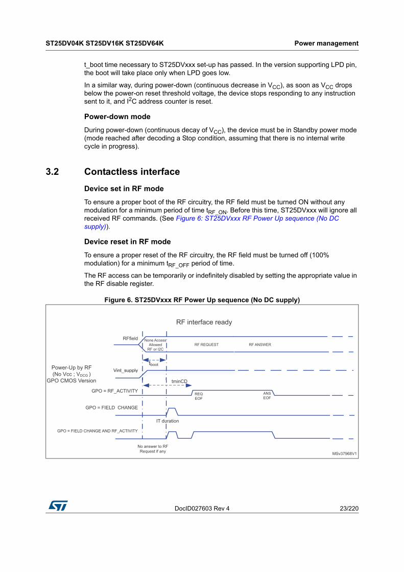
DocID027603 Rev 4 23/220
ST25DV04K ST25DV16K ST25DV64K Power management
219
t_boot time necessary to ST25DVxxx set-up has passed. In the version supporting LPD pin, the boot will take place only when LPD goes low.
In a similar way, during power-down (continuous decrease in VCC), as soon as VCC drops below the power-on reset threshold voltage, the device stops responding to any instruction sent to it, and I2C address counter is reset.
Power-down mode
During power-down (continuous decay of VCC), the device must be in Standby power mode (mode reached after decoding a Stop condition, assuming that there is no internal write cycle in progress).
3.2 Contactless interface
Device set in RF mode
To ensure a proper boot of the RF circuitry, the RF field must be turned ON without any modulation for a minimum period of time tRF_ON. Before this time, ST25DVxxx will ignore all received RF commands. (See Figure 6: ST25DVxxx RF Power Up sequence (No DC supply)).
Device reset in RF mode
To ensure a proper reset of the RF circuitry, the RF field must be turned off (100% modulation) for a minimum tRF_OFF period of time.
The RF access can be temporarily or indefinitely disabled by setting the appropriate value in the RF disable register.
Figure 6. ST25DVxxx RF Power Up sequence (No DC supply)

Memory management ST25DV04K ST25DV16K ST25DV64K
24/220 DocID027603 Rev 4
4 Memory management
4.1 Memory organization overview
The ST25DVxxx memory is divided in four main memory areas:
• User memory
• Dynamic registers
• Fast transfer mode buffer
• System configuration area
The ST25DVxxx user memory can be divided into 4 flexible user areas. Each area can be individually read - and/or - write-protected with one out of three specific 64-bit password.
The ST25DVxxx dynamic registers are accessible by RF or I2C host and provide dynamic activity status or allow temporary activation or deactivation of some ST25DVxxx features.
The ST25DVxxx also provides a 256 byte fast transfer mode buffer, acting as a mailbox between RF and I2C interface, allowing fast data transfer between contact and contactless worlds.
Finally, the ST25DVxxx system configuration area contains static registers to configure all ST25DVxxx features, which can be tuned by user. Its access is protected by a 64 bit configuration password.
This system configuration area also includes read only device information such as IC reference, memory size or IC revision, as well as a 64-bit block that is used to store the 64-bit unique identifier (UID), and the AFI (default 00h) and DSFID (default 00h) registers. The UID is compliant with the ISO 15693 description, and its value is used during the anticollision sequence (Inventory). The UID value is written by ST on the production line. The AFI register stores the application family identifier. The DSFID register stores the data storage family identifier used in the anticollision algorithm.
The system configuration area includes five additional 64-bit blocks that store an I2C password plus three RF user area access passwords and a RF configuration password.

DocID027603 Rev 4 25/220
ST25DV04K ST25DV16K ST25DV64K Memory management
219
Figure 7. Memory organization
4.2 User memory
User memory is accessible from both RF contactless interface and I2C wired interface.
From RF interface, user memory is addressed as Blocks of 4 bytes, starting at address 0. RF extended read and write commands can be used to address all ST25DVxxx memory blocks. Other read and write commands can only address up to block FFh.
From I2C interface, user memory is addressed as Bytes, starting at address 0. Device select must set E2 = 0. User memory can be read in continuity. Unlike the RF interface, there is no roll-over when the requested address reaches the end of the memory capacity.
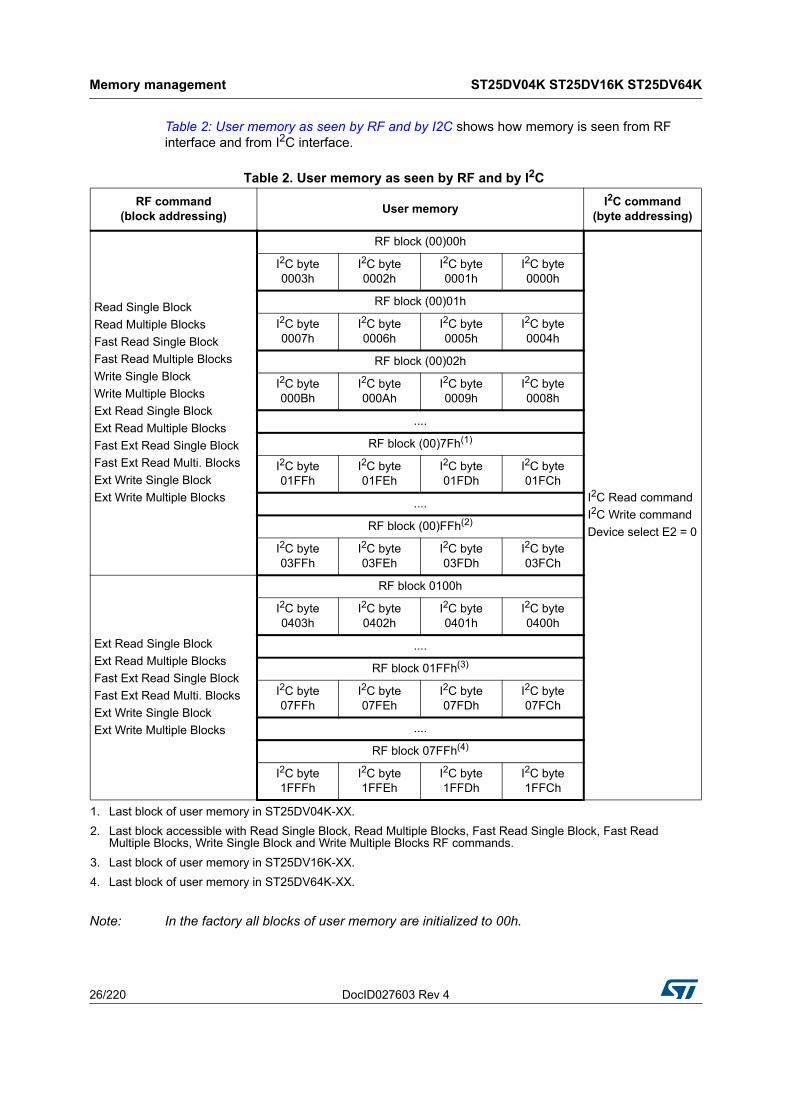
Memory management ST25DV04K ST25DV16K ST25DV64K
26/220 DocID027603 Rev 4
Table 2: User memory as seen by RF and by I2C shows how memory is seen from RF interface and from I2C interface.
Note: In the factory all blocks of user memory are initialized to 00h.
Table 2. User memory as seen by RF and by I2C
RF command(block addressing)
User memoryI2C command
(byte addressing)
Read Single Block
Read Multiple Blocks
Fast Read Single Block
Fast Read Multiple Blocks
Write Single Block
Write Multiple Blocks
Ext Read Single Block
Ext Read Multiple Blocks
Fast Ext Read Single Block
Fast Ext Read Multi. Blocks
Ext Write Single Block
Ext Write Multiple Blocks
RF block (00)00h
I2C Read command
I2C Write command
Device select E2 = 0
I2C byte0003h
I2C byte0002h
I2C byte0001h
I2C byte0000h
RF block (00)01h
I2C byte0007h
I2C byte0006h
I2C byte0005h
I2C byte0004h
RF block (00)02h
I2C byte000Bh
I2C byte000Ah
I2C byte0009h
I2C byte0008h
....
RF block (00)7Fh(1)
I2C byte01FFh
I2C byte01FEh
I2C byte01FDh
I2C byte01FCh
....
RF block (00)FFh(2)
I2C byte03FFh
I2C byte03FEh
I2C byte03FDh
I2C byte03FCh
Ext Read Single Block
Ext Read Multiple Blocks
Fast Ext Read Single Block
Fast Ext Read Multi. Blocks
Ext Write Single Block
Ext Write Multiple Blocks
RF block 0100h
I2C byte0403h
I2C byte0402h
I2C byte0401h
I2C byte0400h
....
RF block 01FFh(3)
I2C byte07FFh
I2C byte07FEh
I2C byte07FDh
I2C byte07FCh
....
RF block 07FFh(4)
I2C byte1FFFh
I2C byte1FFEh
I2C byte1FFDh
I2C byte1FFCh
1. Last block of user memory in ST25DV04K-XX.
2. Last block accessible with Read Single Block, Read Multiple Blocks, Fast Read Single Block, Fast Read Multiple Blocks, Write Single Block and Write Multiple Blocks RF commands.
3. Last block of user memory in ST25DV16K-XX.
4. Last block of user memory in ST25DV64K-XX.

DocID027603 Rev 4 27/220
ST25DV04K ST25DV16K ST25DV64K Memory management
219
4.2.1 User memory areas
The user memory can be split into different areas, each one with a distinct access privilege.
RF and I2C read and write commands are legal only within a same zone:
• In RF, a multiple read or a multiple write command is not executed and returns the error code 0Fh if addresses cross the area borders.
• In I2C, a read data always return FFh after crossing an area border. A write command is not acknowledged and not executed if the command crosses the area border.
Each user memory area is defined by its ending block address ENDAi. The starting block address is defined by the end of the preceding area.
There are three ENDAi registers in the configuration system memory, used to define the end block addresses of Area 1, Area 2 and Area 3. The end of Area 4 is always the last block of memory and is not configurable.
Figure 8. ST25DVxxx user memory areas
On factory delivery all ENDAi are set to maximum value, only Area1 exists and includes the full user memory.
A granularity of 8 Blocks (32 Bytes) is offered to code area ending points.
An area’s end limit is coded as followed in ENDAi registers:
• Last RF block address of area = 8 x ENDAi + 7 => ENDAi = int(Last Areai RF block address / 8)
• Last I2C byte address of area = 32 * ENDAi + 31 => ENDAi = int(Last Areai I2C byte
address / 32)
• As a consequence, ENDA1 = 0 means size of Area 1 is 8 blocks (32 Bytes).

Memory management ST25DV04K ST25DV16K ST25DV64K
28/220 DocID027603 Rev 4
Organization of user memory in areas have the following characteristics:
• At least one area exists (Area1), starting at Block/Byte address 0000h and finishing at ENDA1, with ENDA1 = ENDA2 = ENDA3 = End of user memory (factory setting).
• Two Areas could be defined by setting ENDA1 < ENDA2 = ENDA3 = End of user memory.
• Three Areas may be defined by setting ENDA1 < ENDA2 < ENDA3 = End of user memory.
• A maximum of four areas may be defined by setting ENDA1 < ENDA2 < ENDA3 < End of user memory.
• Area 1 specificities
– Start of Area1 is always Block/Byte address 0000h.
– Area1 minimum size is 8 Blocks (32 Bytes) when ENDA1 = 00h.
– Area1 is always readable.
• The last area always finishes on the last user memory Block/Byte address (ENDA4 doesn't exist).
• All areas are contiguous: end of Area(n) + one Block/Byte address is always start of Area(n+1).
Area size programming
RF user must first open the RF configuration security session to write ENDAi registers.
I2C host must first open I2C security session to write ENDAi registers.
Table 3. Maximum user memory Block and Byte addresses and ENDAi value
DeviceLast user memory
block address seen by RF
Last user memory byte address seen by
I2C
Maximum ENDAi value
ST25DV04K-xx 007Fh 01FFh 0Fh
ST25DV16K-xx 01FFh 07FFh 3Fh
ST25DV64K-xx 07FFh 1FFFh FFh
Table 4. Areas and limit calculation from ENDAi registers
Area Seen from RF interface Seen from I2C interface
Area 1Block 0000h
…Block (ENDA1*8)+7
Byte 0000h…
Byte (ENDA1*32)+31
Area 2Block (ENDA1+1)*8
…Block (ENDA2*8)+7
Byte (ENDA1+1)*32…
Byte (ENDA2*32)+31
Area 3Block (ENDA2+1)*8
…Block (ENDA3*8)+7
Byte (ENDA2+1)*32…
Byte (ENDA3*32)+31
Area 4Block (ENDA3+1)*8
…Last memory Block
Byte (ENDA3+1)*32…
Last memory Byte

DocID027603 Rev 4 29/220
ST25DV04K ST25DV16K ST25DV64K Memory management
219
When programming an ENDAi register, the following rule must be respected:
• ENDAi-1 < ENDAi ≤ ENDAi+1 = End of memory.
This means that prior to programming any ENDAi register, its successor (ENDAi+1) must first be programmed to the last Block/Byte of memory:
• Successful ENDA3 programming condition: ENDA2 < ENDA3 ≤ End of user memory
• Successful ENDA2 programming condition: ENDA1 < ENDA2 ≤ ENDA3 = End of user memory
• Successful ENDA1 programming condition: ENDA1 ≤ ENDA2 = ENDA 3 = End of user memory
If this rule is not respected, an error 0Fh is returned in RF, NoAck is returned in I2C, and programming is not done.
In order to respect this rule, the following procedure is recommended when programming Areas size (even for changing only one Area size):
1. Ends of Areas 3 and 2 must first be set to the end of memory while respecting the following order:
a) If ENDA3 ≠ end of user memory, then set ENDA3 = end of memory; else, do not write ENDA3.
b) If ENDA2 ≠ end of user memory, then set ENDA2 = end of memory; else, do not write ENDA2.
2. Then, desired area limits can be set respecting the following order:
a) Set new ENDA1 value.
b) Set new ENDA2 value, with ENDA2 > ENDA1
c) Set new ENDA3 value, with ENDA3 > ENDA2
Example of successive user memory area setting (for a ST25DV64K-xx):
1. Initial state, 2 Areas are defined:
a) ENDA1 = 10h (Last block of Area 1: (10h x 8) + 7 = 0087h)
b) ENDA2 = FFh (Last block of Area 2: (FFh x 8) + 7 = 07FFh)
c) ENDA3 = FFh (No Area 3)
– Area 1 from Block 0000h to 0087h (136 Blocks)
– Area 2 from Block 0088h to 07FFh (1912 Blocks)
– There is no Area 3.
– There is no Area 4.

Memory management ST25DV04K ST25DV16K ST25DV64K
30/220 DocID027603 Rev 4
Programming ENDA3 to FFh in step 2.a would have resulted in into an error, since rule ENDAi-1 < ENDAi would not been respected (ENDA2 = ENDA3 in that case).
Registers for user memory area configuration
2. Split of user memory in four areas:
a) ENDA3 is not updated as it is already set to end of memory.
b) ENDA2 is not updated as it is already set to end of memory.
c) Set ENDA1 = 3Fh (Last block of Area 1: (3Fh x 8) + 7 = 01FFh)
d) Set ENDA2 = 5Fh (Last block of Area 1: (5Fh x 8) + 7 = 02FFh)
e) Set ENDA3 = BFh (Last block of Area 1: (BFh x 8) + 7 = 05FFh)
– Area1 from Block 0000h to 01FFh (512 Blocks)
– Area2 from Block 0200h to 02FFh (256 Blocks)
– Area3 from Block 0300h to 05FFh (768 Blocks)
– Area4 from Block 0600h to 07FFh (512 Blocks).
3. Return to a split in two equal areas:
a) Set ENDA3 = FFh
b) Set ENDA2 = FFh
c) Set ENDA1 = 7Fh (Last block of Area 1: (7Fh x 8) + 7 = 03FFh)
– Area1 from Block 0000h to 03FFh (1024 Blocks)
– Area2 from Block 0400h to 07FFh (1024 Blocks)
– There is no Area3.
– There is no Area4.
Table 5. ENDA1(1)
RF
CommandRead Configuration (cmd code A0h) @05h Write Configuration (cmd code A1h) @05h
TypeR always, W if RF configuration security session is open and configuration not locked
I2CAddress E2 = 1, 0005h
Type R always, W if I2C security session is open
Bit Name Function Factory Value
b7-b0 ENDA1End Area 1 = 8*ENDA1+7 when expressed in blocks (RF)
End Area 1 = 32*ENDA1+31 when expressed in bytes (I2C)
ST25DV04K-XX: 0Fh
ST25DV16K-XX: 3Fh
ST25DV64K-XX: FFh
1. Refer to Table 8: System configuration memory map for the ENDA1 register.

DocID027603 Rev 4 31/220
ST25DV04K ST25DV16K ST25DV64K Memory management
219
4.3 System configuration area
In addition to EEPROM user memory, ST25DVxxx includes a set of static registers located in the system configuration area memory (EEPROM nonvolatile registers). Those registers are set during device configuration (i.e.: area extension), or by the application (i.e.: area protection). Static registers content is read during the boot sequence and define basic ST25DVxxx behavior.
In RF, the static registers located in the system configuration area can be accessed via dedicated Read Configuration and Write Configuration commands, with a pointer acting as the register address.
The RF configuration security session must first be open, by presenting a valid RF configuration password, to grant write access to system configuration registers.
The system configuration area write access by RF can also be deactivated by I2C host.
Table 6. ENDA2(1)
RF
CommandRead Configuration (cmd code A0h) @07h Write Configuration (cmd code A1h) @07h
TypeR always, W if RF configuration security session is open and configuration not locked
I2CAddress E2 = 1, 0007h
Type R always, W if I2C security session is open
Bit Name Function Factory Value
b7-b0 ENDA2End Area 2 = 8 x ENDA2 + 7 when expressed in blocks (RF)
End Area 2 = 32*ENDA2 + 31 when expressed in bytes (I2C)
ST25DV04K-XX: 0Fh
ST25DV16K-XX: 3Fh
ST25DV64K-XX: FFh
1. Refer to Table 8: System configuration memory map for the ENDA2 register.
Table 7. ENDA3(1)
RF
Command Read Configuration (cmd code A0h) @09h Write Configuration (cmd code A1h) @09h
Type R always, W if RF configuration security session is open and configuration not locked
I2CAddress E2 = 1, 0009h
Type R always, W if I2C security session is open
Bit Name Function Factory Value
b7-b0 ENDA3End Area 3 = 8 x ENDA3 + 7 when expressed in blocks (RF)
End Area 3 = 32 x ENDA3 + 31 when expressed in bytes (I2C)
ST25DV04K-XX: 0Fh
ST25DV16K-XX: 3Fh
ST25DV64K-XX: FFh
1. Refer to Table 8: System configuration memory map for the ENDA3 register.
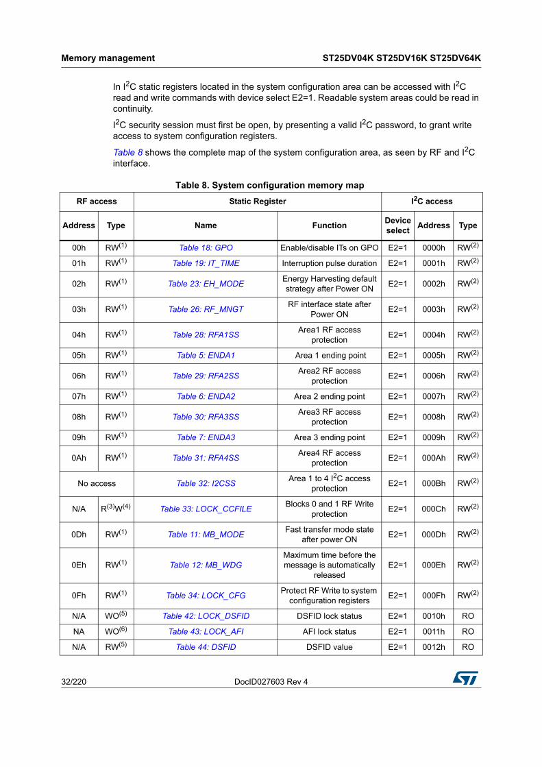
Memory management ST25DV04K ST25DV16K ST25DV64K
32/220 DocID027603 Rev 4
In I2C static registers located in the system configuration area can be accessed with I2C read and write commands with device select E2=1. Readable system areas could be read in continuity.
I2C security session must first be open, by presenting a valid I2C password, to grant write access to system configuration registers.
Table 8 shows the complete map of the system configuration area, as seen by RF and I2C interface.
Table 8. System configuration memory map
RF access Static Register I2C access
Address Type Name FunctionDevice select
Address Type
00h RW(1) Table 18: GPO Enable/disable ITs on GPO E2=1 0000h RW(2)
01h RW(1) Table 19: IT_TIME Interruption pulse duration E2=1 0001h RW(2)
02h RW(1) Table 23: EH_MODEEnergy Harvesting default strategy after Power ON
E2=1 0002h RW(2)
03h RW(1) Table 26: RF_MNGTRF interface state after
Power ONE2=1 0003h RW(2)
04h RW(1) Table 28: RFA1SSArea1 RF access
protectionE2=1 0004h RW(2)
05h RW(1) Table 5: ENDA1 Area 1 ending point E2=1 0005h RW(2)
06h RW(1) Table 29: RFA2SSArea2 RF access
protection E2=1 0006h RW(2)
07h RW(1) Table 6: ENDA2 Area 2 ending point E2=1 0007h RW(2)
08h RW(1) Table 30: RFA3SSArea3 RF access
protection E2=1 0008h RW(2)
09h RW(1) Table 7: ENDA3 Area 3 ending point E2=1 0009h RW(2)
0Ah RW(1) Table 31: RFA4SSArea4 RF access
protectionE2=1 000Ah RW(2)
No access Table 32: I2CSSArea 1 to 4 I2C access
protectionE2=1 000Bh RW(2)
N/A R(3)W(4) Table 33: LOCK_CCFILEBlocks 0 and 1 RF Write
protectionE2=1 000Ch RW(2)
0Dh RW(1) Table 11: MB_MODEFast transfer mode state
after power ONE2=1 000Dh RW(2)
0Eh RW(1) Table 12: MB_WDGMaximum time before the message is automatically
releasedE2=1 000Eh RW(2)
0Fh RW(1) Table 34: LOCK_CFGProtect RF Write to system
configuration registersE2=1 000Fh RW(2)
N/A WO(5) Table 42: LOCK_DSFID DSFID lock status E2=1 0010h RO
NA WO(6) Table 43: LOCK_AFI AFI lock status E2=1 0011h RO
N/A RW(5) Table 44: DSFID DSFID value E2=1 0012h RO

DocID027603 Rev 4 33/220
ST25DV04K ST25DV16K ST25DV64K Memory management
219
N/A RW(6) Table 45: AFI AFI value E2=1 0013h RO
N/ARO Table 46: MEM_SIZE
Memory size value in blocks, 2 bytes
E2=10014h
to0015h
RO
RO Table 47: BLK_SIZE Block size value in bytes E2=1 0016h RO
N/A RO Table 48: IC_REF IC reference value E2=1 0017h RO
NA RO Table 49: UID Unique identifier, 8 bytes E2=10018h
to001Fh
RO
No access
Table 50: IC_REV IC revision E2=1 0020h RO
- ST Reserved E2=1 0021h RO
- ST Reserved E2=1 0022h RO
- ST Reserved E2=1 0023h RO
Table 35: I2C_PWDI2C security session password, 8 bytes
E2=1
0900h
to
0907h
R(7)/W(8)
N/A WO(9) Table 36: RF_PWD_0RF configuration security
session password, 8 bytes
No access
N/A WO(9) Table 37: RF_PWD_1RF user security session
password 1, 8 bytes
N/A WO(9) Table 38: RF_PWD_2RF user security session
password 2, 8 bytes
N/A WO(9) Table 39: RF_PWD_3RF user security session
password 3, 8 bytes
1. Write access is granted if RF configuration security session is open and configuration is not locked (LOCK_CFG register equals to 0).
2. Write access if I2C security session is open.
3. LOCK_CCFILE content is only readable through reading the Block Security Status of blocks 00h and 001h (see Section 5.6.3: User memory protection)
4. Write access to bit 0 if Block 00h is not already locked and to bit 1 if Block 01h is not already locked.
5. Write access if DSFID is not locked
6. Write access if AFI is not locked.
7. Read access is granted if I2C security session is open.
8. Write access with I2C Write Password command, only after presenting a correct I2C password.
9. Write access only if corresponding RF security session is open.
Table 8. System configuration memory map (continued)
RF access Static Register I2C access
Address Type Name FunctionDevice select
Address Type
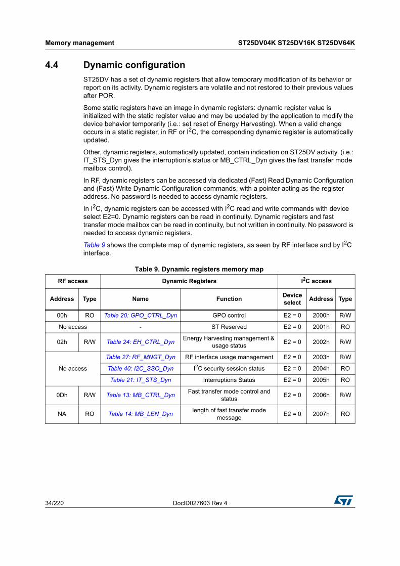
Memory management ST25DV04K ST25DV16K ST25DV64K
34/220 DocID027603 Rev 4
4.4 Dynamic configuration
ST25DV has a set of dynamic registers that allow temporary modification of its behavior or report on its activity. Dynamic registers are volatile and not restored to their previous values after POR.
Some static registers have an image in dynamic registers: dynamic register value is initialized with the static register value and may be updated by the application to modify the device behavior temporarily (i.e.: set reset of Energy Harvesting). When a valid change occurs in a static register, in RF or I2C, the corresponding dynamic register is automatically updated.
Other, dynamic registers, automatically updated, contain indication on ST25DV activity. (i.e.: IT_STS_Dyn gives the interruption’s status or MB_CTRL_Dyn gives the fast transfer mode mailbox control).
In RF, dynamic registers can be accessed via dedicated (Fast) Read Dynamic Configuration and (Fast) Write Dynamic Configuration commands, with a pointer acting as the register address. No password is needed to access dynamic registers.
In I2C, dynamic registers can be accessed with I2C read and write commands with device select E2=0. Dynamic registers can be read in continuity. Dynamic registers and fast transfer mode mailbox can be read in continuity, but not written in continuity. No password is needed to access dynamic registers.
Table 9 shows the complete map of dynamic registers, as seen by RF interface and by I2C interface.
Table 9. Dynamic registers memory map
RF access Dynamic Registers I2C access
Address Type Name FunctionDeviceselect
Address Type
00h RO Table 20: GPO_CTRL_Dyn GPO control E2 = 0 2000h R/W
No access - ST Reserved E2 = 0 2001h RO
02h R/W Table 24: EH_CTRL_DynEnergy Harvesting management &
usage statusE2 = 0 2002h R/W
No access
Table 27: RF_MNGT_Dyn RF interface usage management E2 = 0 2003h R/W
Table 40: I2C_SSO_Dyn I2C security session status E2 = 0 2004h RO
Table 21: IT_STS_Dyn Interruptions Status E2 = 0 2005h RO
0Dh R/W Table 13: MB_CTRL_DynFast transfer mode control and
statusE2 = 0 2006h R/W
NA RO Table 14: MB_LEN_Dynlength of fast transfer mode
messageE2 = 0 2007h RO

DocID027603 Rev 4 35/220
ST25DV04K ST25DV16K ST25DV64K Memory management
219
4.5 Fast transfer mode mailbox
ST25DVxxx fast transfer mode uses a dedicated mailbox buffer for transferring messages between RF and I2C worlds. This mailbox contains up to 256 Bytes of data which are filled from the first byte.
Fast transfer mode mailbox is accessed in bytes from both RF and I2C.
In RF, mailbox is read via a dedicated (Fast) Read Message command. Read can start from any address value inside the mailbox, between 00h and FFh. Writing in the mailbox is done via the (Fast) Write Message command in one shot, always starting at mailbox address 00h. No password is needed to access mailbox from RF, but fast transfer mode must be enabled.
In I2C, mailbox read can start from any address value between 2008h and 2107h. Write mailbox MUST start from address 2008h to a max of 2107h. No password is needed to access mailbox from I2C, but fast transfer mode must be enabled.
Table 10 shows the map of fast transfer mode mailbox, as seen by RF interface and by I2C interface.
Table 10. Fast transfer mode mailbox memory map
RF access Fast transfer mode buffer I2C access
Address Type Name FunctionDeviceselect
Address Type
00h R/W MB_Dyn Byte 0
Fast transfer mode buffer (256-Bytes)
E2 = 0 2008h R/W
01h R/W MB_Dyn Byte 1 E2 = 0 2009h R/W
… … … E2 = 0 ... ...
FEh R/W MB_Dyn Byte 254 E2 = 0 2106h R/W
FFh R/W MB_Dyn Byte 255 E2 = 0 2107h R/W

ST25DVxxx specific features ST25DV04K ST25DV16K ST25DV64K
36/220 DocID027603 Rev 4
5 ST25DVxxx specific features
ST25DVxxx offers the following features:
• A fast transfer mode (FTM), to achieve a fast link between RF and contact worlds, via a 256 byte buffer called Mailbox. This mailbox dynamic buffer of 256 byte can be filled or emptied via either RF or I2C.
• A GPO pin, which indicates incoming event to the contact side, like RF Field changes, RF activity in progress, RF writing completion or Mailbox message availability.
• An Energy Harvesting element to deliver µW of power when external conditions make it possible.
• RF management, which allows ST25DVxxx to ignore RF requests.
All these features can be programmed by setting static and/or dynamic registers of the ST25DVxxx. ST25DVxxx can be partially customized using configuration registers located in the E2 system area.
These registers are:
• dedicated to Data Memory organization and protection ENDAi, I2CSS, RFAiSS, LOCK_CCFILE.
• dedicated to fast transfer mode MB_WDG, MB_MODE
• dedicated to observation, GPO, IT_TIME
• dedicated to RF , RF_MNGT, EH_MODE
• dedicated the device’s structure LOCK_CFG
A set of additional registers allows to identify and customize the product (DSFID, AFI, IC_REF, etc.).
In I²C,
Read accesses to the static configuration register is always allowed, except for passwords. For dedicated registers, write access is granted after prior successful presentation of the I2C password. Configuration register are located from @00h to 0Fh in the system area (device code 111)
In RF
Dedicated commands Read Configuration and Write Configuration must be used to access the static configuration registers. Update is only possible when the access right was granted by presenting the RF configuration password (RF_PWD_0), and if the system configuration was not previously locked by the I2C host (LOCK_CFG=1), which acts as security master.
After any valid write access to the static configuration registers, the new configuration is immediately applied.
Some of the static registers have a dynamic image (notice _Dyn) preset with the static register value: GPO_CTRL_Dyn, EH_CTRL_Dyn, RF_MNGT_Dyn and MB_CTRL_Dyn.
When it exists, ST25DVxxx uses the dynamic configuration register to manage its processes. A dynamic configuration register updated by the application will recover its default static value after a Power On Reset (POR).

DocID027603 Rev 4 37/220
ST25DV04K ST25DV16K ST25DV64K ST25DVxxx specific features
219
Other dynamic registers are dedicated to process monitoring:
• I2C_SSO_Dyn is dedicated to data memory protection
• MB_LEN_Dyn, MB_CTRL_Dyn are dedicated to fast transfer mode
• IT_STS_Dyn is dedicated to interrupt
In I2C, read and write of the Dynamic registers is done using usual I2C read & write command at dedicated address. (E2 =0 in device select).
In RF read or write accesses to the Dynamic registers are associated to the dedicated commands, Read Dynamic Configuration, Write Dynamic Configuration and Read Message Length.
5.1 Fast transfer mode (FTM)
5.1.1 Fast transfer mode registers
Static Registers
Table 11. MB_MODE(1)
RF
CommandRead Configuration (cmd code A0h) @0Dh Write Configuration (cmd code A1h) @0Dh
TypeR always, W if RF configuration security session is open and configuration not locked
I2CAddress E2=1, 000Dh
Type R always, W if I2C security session is open
Bit Name Function Factory Value
b0 MB_MODE0: Enabling fast transfer mode is forbidden.
1: Enabling fast transfer mode is authorized.0b
b7-b1 RFU - 0000000b
1. Refer to Table 8: System configuration memory map for the MB_MODE register.

ST25DVxxx specific features ST25DV04K ST25DV16K ST25DV64K
38/220 DocID027603 Rev 4
Dynamic Registers
Table 12. MB_WDG(1)
RF
CommandRead Configuration (cmd code A0h) @0Eh Write Configuration (cmd code A1h) @0Eh
TypeR always, W if RF configuration security session is open and configuration not locked
I2CAddress E2=1, 000Eh
Type R always, W if I2C security session is open
Bit Name Function Factory Value
b2-b0 MB_WDG
If MB_WDG = 0, then watchdog duration is infinite111b
b7-b3 RFU - 00000b
1. Refer to Table 8: System configuration memory map for the MB_WDG register.
Watch dog duration = 2MB_WDG 1–( )
30ms× 6±
Table 13. MB_CTRL_Dyn(1)
RFCommand
Read Dynamic Configuration (cmd code ADh) @0Dh Fast Read Dynamic Configuration (cmd code CDh) @0Dh Write Dynamic Configuration (cmd code AEh) @0Dh Fast Write Dynamic Configuration (cmd code CEh) @0Dh
Type b0: R always, W – b7-b1: RO
I2CAddress E2 = 0, 2006h
Type b0: R always, W - b7 - b1: RO
Bit Name Function Factory Value
b0 MB_EN(2) 0: Disable FTM, FTM mailbox is empty
1: Enable FTM0b
b1 HOST_PUT_MSG0: No I2C message in FTM mailbox
1: I2C has Put a message in FTM mailbox0b
b2 RF_PUT_MSG0: No RF message in FTM mailbox
1: RF has Put message in FTM mailbox 0b

DocID027603 Rev 4 39/220
ST25DV04K ST25DV16K ST25DV64K ST25DVxxx specific features
219
5.1.2 Fast transfer mode usage
ST25DV acts as mailbox between RF (reader, smartphone, ...) and an I2C host (microcontroller...). Each interface can send a message containing up to 256 bytes of data to the other interface through that mailbox.
To send data from RF reader to I2C host, fast transfer mode must be enabled, the mailbox must be free, and the RF user must first writes the message containing data in the mailbox.
b3 RFU - 0b
b4 HOST_MISS_MSG0: No message missed by I2C
1: I2C did not read RF message before watchdog time out0b
b5 RF_MISS_MSG0: No message missed by RF
1: RF did not read message before watchdog time out0b
b6 HOST_CURRENT_MSG0: No message or message not coming from I2C
1: Current Message in FTM mailbox comes from I2C0b
b7 RF_CURRENT_MSG0: No message or message not coming from RF
1: Current Message in FTM mailbox comes from RF0b
1. Refer to Table 9: Dynamic registers memory map for the MB_CTRL_Dyn register.
2. MB_EN bit is automatically reset to 0 if MB_MODE register is reset to 0.
Table 13. MB_CTRL_Dyn(1) (continued)
RFCommand
Read Dynamic Configuration (cmd code ADh) @0Dh Fast Read Dynamic Configuration (cmd code CDh) @0Dh Write Dynamic Configuration (cmd code AEh) @0Dh Fast Write Dynamic Configuration (cmd code CEh) @0Dh
Type b0: R always, W – b7-b1: RO
I2CAddress E2 = 0, 2006h
Type b0: R always, W - b7 - b1: RO
Bit Name Function Factory Value
Table 14. MB_LEN_Dyn(1)
RFCommand
Read Message Lenght (cmd code ABh) Fast Read Message Lenght (cmd code CBh)
Type RO
I2CAddress E2 = 0, 2007h
Type RO
Bit Name Function Factory Value
b7-b0 MB_LENSize in byte of message contained in FTM mailbox (automatically set by ST25DVxxx)
0h
1. Refer to Table 9: Dynamic registers memory map for the MB_LEN_Dyn register.
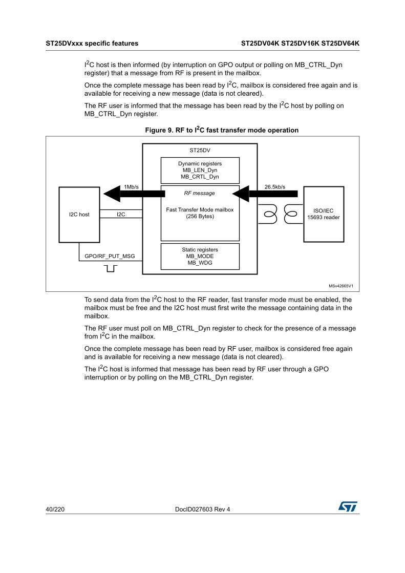
ST25DVxxx specific features ST25DV04K ST25DV16K ST25DV64K
40/220 DocID027603 Rev 4
I2C host is then informed (by interruption on GPO output or polling on MB_CTRL_Dyn register) that a message from RF is present in the mailbox.
Once the complete message has been read by I2C, mailbox is considered free again and is available for receiving a new message (data is not cleared).
The RF user is informed that the message has been read by the I2C host by polling on MB_CTRL_Dyn register.
Figure 9. RF to I2C fast transfer mode operation
To send data from the I2C host to the RF reader, fast transfer mode must be enabled, the mailbox must be free and the I2C host must first write the message containing data in the mailbox.
The RF user must poll on MB_CTRL_Dyn register to check for the presence of a message from I2C in the mailbox.
Once the complete message has been read by RF user, mailbox is considered free again and is available for receiving a new message (data is not cleared).
The I2C host is informed that message has been read by RF user through a GPO interruption or by polling on the MB_CTRL_Dyn register.

DocID027603 Rev 4 41/220
ST25DV04K ST25DV16K ST25DV64K ST25DVxxx specific features
219
Figure 10. I2C to RF fast transfer mode operation
VCC supply source is mandatory to activate this feature.
No precedence rule is applied: the first request is served first.
Adding a message is only possible when fast transfer mode is enabled (MB_EN=1) and mailbox is free (HOST_PUT_MSG and RF_PUT_MSG cleared, which is the case after POR or after complete reading of I2C message by RF, and complete reading of RF message by I2C).
A watchdog limits the message availability in time: when a time-out occurs, the mailbox is considered free, and the HOST_MISS_MSG or RF_MISS_MSG bits is set into MB_CTRL_Dyn register. The data contained in the mailbox is not cleared after a read or after the watchdog has been triggered: message data is still available for read and until fast transfer mode is disabled. HOST_CURRENT_MSG and RF_CURRENT_MSG bits are indicating the source of the current data.
The message is stored in a buffer (256 Bytes), and the write operation is done immediately. .
Caution: The data written in user or system memory (EEPROM), either from I2C or from RF, transits via the 256-Bytes fast transfer mode's buffer. Consequently fast transfer mode must be deactivated (MB_EN=0) before starting any write operation in user or system memory, otherwise command will be NotACK for I2C or get an answer 0Fh for RF and programming is not done.
I2C access to mailbox
The access by I2C can be done by dedicated address mapping to mailbox (2008h to 2107h) with device identifier E2 = 0.
I2C reading operation does not support rollover. Therefore data out is set to FFh when the counter reaches the message end.
The RF_PUT_MSG is cleared after reaching the STOP consecutive to reading the last message byte, and the mailbox is considered free (but the message is not cleared and it is still present in the mailbox).

ST25DVxxx specific features ST25DV04K ST25DV16K ST25DV64K
42/220 DocID027603 Rev 4
A I2C reading operation will never clear HOST_PUT_MSG, and the message remains available for RF.
An I2C read can start at any address inside the mailbox (between address 2008h and 2107h).
A I2C write operation must start from the first mailbox location, at address 2008h. After reaching the Mailbox border at address 2107h all bytes are NACK and the command is not executed (rollover feature not supported).
At the end of a successful I2C message write, the message length is automatically set into MB_LEN_Dyn register, and HOST_PUT_MSG bit is set into MB_CTRL_Dyn register, and the write access to the mailbox is not possible until the mailbox has been released again.
RF access to mailbox
The RF Control & Access to mailbox is possible using dedicated custom commands:
• Read Dynamic Configuration and Fast Read Dynamic Configuration to check availability of mailbox.
• Write Dynamic Configuration and Fast Write Dynamic configuration to enable or disable fast transfer mode.
• Read Message Length and Fast Read Message Length to get the length of the contained message,
• Read Message and Fast Read Message to download the content of the mailbox,
• Write Message and Fast Write Message to put a new message in mailbox. (New length is automatically updated after completion of a successful Write Message or Fast Write Message command).
HOST_PUT_MSG is cleared following a valid reading of the last message byte, and mailbox is considered free (but message is not cleared and is still present in the mailbox).
A RF read can start at any address of inside the message, but return an error 0Fh if trying to read after the last byte of the message.
A RF reading operation will never clear RF_PUT_MSG , the message will remain available for I2C.
At the end of a successful RF message write, the message length is automatically set in MB_LEN_Dyn register, and RF_PUT_MSG bit is set in MB_CTRL_Dyn register. and write access to the mailbox is not possible until mailbox has been freed again.
The presence of a DC supply is mandatory to get RF access to the mailbox. VCC_ON can be checked reading the dynamic register EH_CTRL_Dyn.
To get more details about sequences to prepare and initiate a Fast Transfer, to detect progress of a fast transfer or to control and execute a fast transfer, please refer to AN4910. How to exchange data between wired (I2C) and wireless world (RF ISO15693) using fast transfer mode supported by ST25DVxxx).
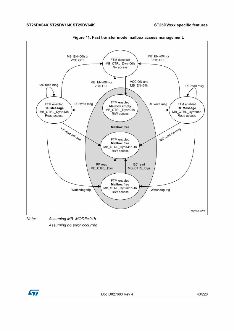
DocID027603 Rev 4 43/220
ST25DV04K ST25DV16K ST25DV64K ST25DVxxx specific features
219
Figure 11. Fast transfer mode mailbox access management.
Note: Assuming MB_MODE=01h
Assuming no error occurred

ST25DVxxx specific features ST25DV04K ST25DV16K ST25DV64K
44/220 DocID027603 Rev 4
5.2 GPO
GPO signal is used to alert the I2C host of external RF events or ST25DVxxx processes activity. Several causes could be used to request a host interruption. RF user can also directly drive GPO pin level using a dedicated RF command.
5.2.1 ST25DVxxx interrupt capabilities on RF events
ST25DVxxx supports multi interruption mode and can report several events occurring through RF interface.
In this chapter, all drawings are referring to the open drain version of GPO output (ST25DVxxK-IE).
The reader can retrieve the behavior of CMOS version (ST25DVxxK-JF) by inverting the GPO curve polarity and replace in text “released” or “high-Z” by “pull to ground”.
Supported RF events is listed hereafter:

DocID027603 Rev 4 45/220
ST25DV04K ST25DV16K ST25DV64K ST25DVxxx specific features
219
RF_USER:
• GPO output level is controlled by Manage GPO command (set or reset)
• When RF_USER is activated, GPO level is changed after EOF of ST25DV response to a Manage GPO set or reset command (see Section 7.6.30: Manage GPO).
• RF_USER is prevalent over all other GPO events when set by Manage GPO command (other interrupts are still visible in IT_STS_Dyn status register, but do not change GPO output level).
Figure 12. RF_USER chronogram

ST25DVxxx specific features ST25DV04K ST25DV16K ST25DV64K
46/220 DocID027603 Rev 4
RF_ACTIVITY:
• GPO output level reflects the RF activity.
• When RF_ACTIVITY is activated, a GPO output level change from RF command EOF to ST25DV response EOF.
Figure 13. RF_ACTIVITY chronogram
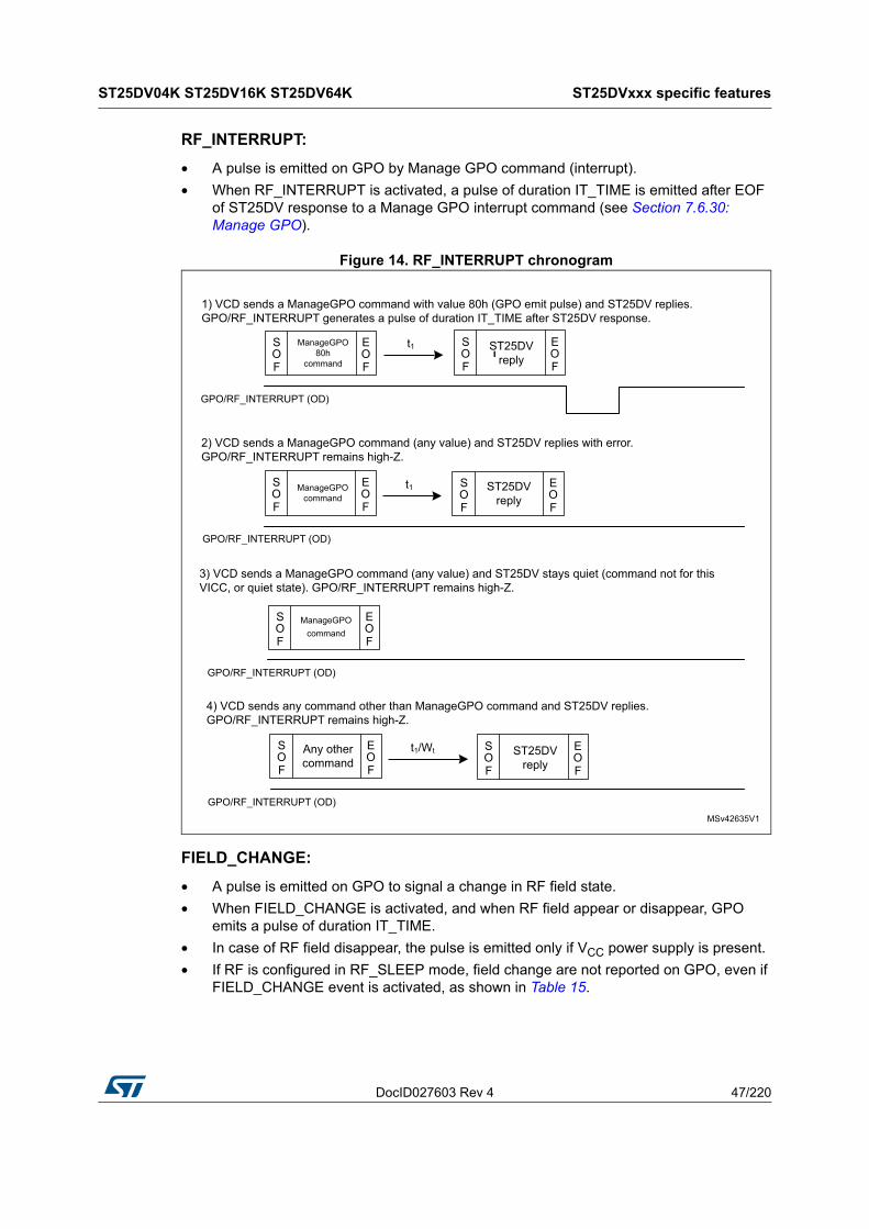
DocID027603 Rev 4 47/220
ST25DV04K ST25DV16K ST25DV64K ST25DVxxx specific features
219
RF_INTERRUPT:
• A pulse is emitted on GPO by Manage GPO command (interrupt).
• When RF_INTERRUPT is activated, a pulse of duration IT_TIME is emitted after EOF of ST25DV response to a Manage GPO interrupt command (see Section 7.6.30: Manage GPO).
Figure 14. RF_INTERRUPT chronogram
FIELD_CHANGE:
• A pulse is emitted on GPO to signal a change in RF field state.
• When FIELD_CHANGE is activated, and when RF field appear or disappear, GPO emits a pulse of duration IT_TIME.
• In case of RF field disappear, the pulse is emitted only if VCC power supply is present.
• If RF is configured in RF_SLEEP mode, field change are not reported on GPO, even if FIELD_CHANGE event is activated, as shown in Table 15.

ST25DVxxx specific features ST25DV04K ST25DV16K ST25DV64K
48/220 DocID027603 Rev 4
Figure 15. FIELD_CHANGE chronogram
RF_PUT_MSG:
• A pulse is emitted on GPO when a message is successfully written by RF in fast transfer mode mailbox.
• When RF_PUT_MSG is activated, a pulse of duration IT_TIME is emitted on GPO at completion of valid Write Message or Fast Write Message commands (after EOF of ST25DV response).
Table 15. FIELD_CHANGE when RF is disabled or in sleep mode
RF_DISABLE RF_SLEEP GPO behavior when FIELD_DETECT is enabled
0 0A pulse is emitted on GPO if RF field appears or disappears(1)
1. assuming that GPO output is enabled (GPO_EN = 1).
1 0
X 1 GPO remains High-Z (OD) or tied low (CMOS)
IT_STS_Dyn register is not updated.X 1

DocID027603 Rev 4 49/220
ST25DV04K ST25DV16K ST25DV64K ST25DVxxx specific features
219
Figure 16. RF_PUT_MSG chronogram
RF_GET_MSG:
• A pulse is emitted on GPO when RF has successfully read a message, up to its last byte, in fast transfer mode mailbox.
• When RF_GET_MSG is activated, a pulse of duration IT_TIME is emitted on GPO at completion of valid Read Message or Fast Read Message commands (after EOF of ST25DV response), and end of message has been reached.
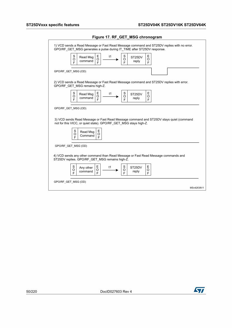
ST25DVxxx specific features ST25DV04K ST25DV16K ST25DV64K
50/220 DocID027603 Rev 4
Figure 17. RF_GET_MSG chronogram

DocID027603 Rev 4 51/220
ST25DV04K ST25DV16K ST25DV64K ST25DVxxx specific features
219
RF_WRITE:
• When RF_WRITE is activated, a pulse of duration IT_TIME is emitted at completion of a valid RF write operation in EEPROM (after EOF of ST25DV response).
• Following commands trigger the RF_WRITE interrupt after a valid write operation in EEPROM:
– Write Single Block
– Extended Write Single Block
– Write Multiple Block
– Extended Write Multiple Block
– Lock Block
– Extended Lock Block
– Write AFI
– Lock AFI
– Write DSFID
– Lock DSFID
– Write Configuration
– Write Password
• Note that writing in dynamic registers or fast transfer mode mailbox does not trigger RF_WRITE interrupt (no write operation in EEPROM).

ST25DVxxx specific features ST25DV04K ST25DV16K ST25DV64K
52/220 DocID027603 Rev 4
Figure 18. RF_WRITE chronogram
5.2.2 GPO and power supply
When at the same time RF field is present and VCC is ON, GPO is acting as configured in GPO, GPO_CTRL_Dyn and IT_TIME registers.
When the RF field disappears, the GPO state is reset and the output level is set to high-Z (open drain) or tied low (CMOS). Interruption status in IT_STS_Dyn register is maintained until next I2C read or VCC power off.

DocID027603 Rev 4 53/220
ST25DV04K ST25DV16K ST25DV64K ST25DVxxx specific features
219
When VCC is not present, or ST25DVxxx is in low power mode, all events are available on GPO pin, assuming pull-up resistor is supplied with correct voltage (Open Drain-IE version) or VDCG is powered (CMOS-JF version). Host can be waken up using GPO interrupt in any power condition.
Exception is FIELD_CHANGE when RF field is falling, which can’t be reported on GPO output if VCC is off (no power supply on ST25DVxxx)
5.2.3 GPO registers
Four registers are dedicated to this feature:
• Two static registers in system configuration
• Two dynamic registers
Table 16. GPO interrupt capabilities in function of RF field
RF field on RF field off
GPO state is function of RF events(1)
1. If pull-up resistor is powered (Open Drain-IE version), and VDCG is powered (CMOS –JF version).
GPO remains High-Z (OD) or tied low (CMOS)
Table 17. GPO interrupt capabilities in function of VCC power supply
GPO events VCC OFFVCC ON and LPD high(1)
(low power mode)
1. For STM25DVxxK-JF only.
VCC ON andLPD low(1)
FIELD_CHANGE if RF field disappears
GPO remains High-Z (OD) or tied low (CMOS)
Pulse emitted on GPO(2)
2. If pull-up resistor is powered (Open Drain-IE version) and VDCG is powered (CMOS-JF version).
Pulse emitted on GPO
Any other activated RF event
GPO state is function of RF events(2)
GPO state is function of RF events(2)
GPO state is function of RF events(2)

ST25DVxxx specific features ST25DV04K ST25DV16K ST25DV64K
54/220 DocID027603 Rev 4
• Enables the interruption source, and enable GPO output.
• Several interruption sources can be enabled simultaneously.
• The updated value is valid for the next command (except for the RF_WRITE interrupt, which is valid right after EOF of the Write Configuration command if enabled through RF).
• The GPO_EN bit (b7) allows to disable GPO output (High-Z for open drain version, driven low for CMOS version). Interruptions are still reported in IT_STS_Dyn register.
• RF configuration security session (present RF password 0) or I2C security session (present I2C password) must be open in order to write the GPO register.
Table 18. GPO(1)
RF
CommandRead Configuration (cmd code A0h) @00h Write Configuration (cmd code A1h) @00h
TypeR always, W if RF configuration security session is open and configuration not locked
I2CAddress E2=1, 0000h
Type R always, W if I2C security session is open
Bit Name FunctionFactory Value
b0 RF_USER_EN0: disabled
1: GPO output level is controlled by Manage GPO Command (set/reset)0b
b1 RF_ACTIVITY_EN0: disabled
1: GPO output level changes from RF command EOF to response EOF.0b
b2 RF_INTERRUPT_EN0: disabled
1: GPO output level is controlled by Manage GPO Command (pulse).0b
b3 FIELD_CHANGE_EN0: disabled
1: A pulse is emitted on GPO, when RF field appears or disappears.1b
b4 RF_PUT_MSG_EN0: disabled
1: A pulse is emitted on GPO at completion of valid RF Write Message command.
0b
b5 RF_GET_MSG_EN0: disabled
1: A pulse is emitted on GPO at completion of valid RF Read Message command if end of message has been reached.
0b
b6 RF_WRITE_EN0: disabled 1: A pulse is emitted on GPO at completion of valid RF write operation in EEPROM.
0b
b7 GPO_EN0: GPO output is disabled. GPO is High-Z (open drain) or 0 (CMOS)
1: GPO output is enabled. GPO outputs enabled interrupts.1b
1. Refer to Table 8: System configuration memory map for the GPO register.

DocID027603 Rev 4 55/220
ST25DV04K ST25DV16K ST25DV64K ST25DVxxx specific features
219
• Defines interrupt pulse duration on GPO pin for the flowing events: RF_INTERRUPT, FIELD_CHANGE, RF_PUT_MSG, RF_GET_MSG and RF_WRITE.
• See IT pulse duration equation: for interrupt duration calculation.
• RF configuration security session (present RF password 0) or I2C security session (present I2C password) must be open in order to write IT_TIME register.
Table 19. IT_TIME(1)
RF
CommandRead Configuration (cmd code A0h) @01h Write Configuration (cmd code A1h) @01h
TypeR always, W if RF configuration security session is open and configuration not locked
I2CAddress E2=1, 0001h
Type R always, W if I2C security session is open
Bit Name FunctionFactory Value
b2-b0 IT_TIME Pulse duration = 301 us - IT_TIME x 37.65 us ± 2 us 011b
b7-b3 RFU - 00000b
1. Refer to Table 8: System configuration memory map for the IT_TIME register.
Table 20. GPO_CTRL_Dyn(1)
RFCommand
Read Dynamic Configuration (cmd code ADh) @00h Write Dynamic Configuration (cmd code AEh) @00h
Fast Read Dynamic Configuration (cmd code CDh) @00h
Fast Write Dynamic Configuration (cmd code CEh) @00h
Type RO
I2CAddress E2 = 0, 2000h
Type b0-b6: RO - b7 : R always, W always
Bit Name FunctionFactory Value
b0 RF_USER_EN0: disabled
1: GPO output level is controlled by Manage GPO Command (set/reset)0b
b1 RF_ACTIVITY_EN0: disabled
1: GPO output level changes from RF command SOF to response EOF.0b
b2 RF_INTERRUPT_EN0: disabled
1: GPO output level is controlled by Manage GPO Command (pulse).0b

ST25DVxxx specific features ST25DV04K ST25DV16K ST25DV64K
56/220 DocID027603 Rev 4
• Allows I2C host to dynamically enable or disable GPO output by writing in GPO_EN bit (b7).
• GPO_EN bit of GPO_CTRL_Dyn register is prevalent over GPO_EN bit of GPO register.
• At power up, and each time GPO register is updated, GPO_CTRL_Dyn content is copied from GPO register.
• GPO_CTRL_Dyn is a volatile register. Value is maintained only if at least one of the two power sources is present (RF field or VCC).
• GPO_CTRL_Dyn bit 7 (GPO_EN) can be written even if I2C security session is closed (I2C password not presented) but is read only for RF user.
• Modifying GPO_CTRL_Dyn, the bit 7 GPO_EN does not affect the value of GPO register bit 7 GPO_EN
b3 FIELD_CHANGE_EN0: disabled
1: A pulse is emitted on GPO, when RF field appears or disappears.1b
b4 RF_PUT_MSG_EN0: disabled
1: A pulse is emitted on GPO at completion of valid RF Write Message command.
0b
b5 RF_GET_MSG_EN0: disabled
1: A pulse is emitted on GPO at completion of valid RF Read Message command if end of message has been reached.
0b
b6 RF_WRITE_EN0: disabled 1: A pulse is emitted on GPO at completion of valid RF write operation in EEPROM.
0b
b7 GPO_EN0: GPO output is disabled. GPO is High-Z (open drain) or 0 (CMOS)
1: GPO output is enabled. GPO outputs enabled interrupts.1b
1. Refer to Table 9: Dynamic registers memory map for the GPO_CTRL_Dyn register.
Table 20. GPO_CTRL_Dyn(1) (continued)
RFCommand
Read Dynamic Configuration (cmd code ADh) @00h Write Dynamic Configuration (cmd code AEh) @00h
Fast Read Dynamic Configuration (cmd code CDh) @00h
Fast Write Dynamic Configuration (cmd code CEh) @00h
Type RO
I2CAddress E2 = 0, 2000h
Type b0-b6: RO - b7 : R always, W always
Bit Name FunctionFactory Value

DocID027603 Rev 4 57/220
ST25DV04K ST25DV16K ST25DV64K ST25DVxxx specific features
219
• Cumulates all events which generate interruptions. It should be checked by I2C host to know which event triggered an interrupt on GPO pin.
• When enabled, RF events are reported in IT_STS_Dyn register even if GPO output is disabled though the GPO_EN bit.
• Once read the ITSTS_Dyn register is cleared (set to 00h).
• At power up, IT_STS_Dyn content is cleared (set to 00h).
• IT_STS_Dyn is a volatile register. Value is maintained only if at least one of the two power sources is present (RF field or VCC).
5.2.4 Configuring GPO
GPO and interruption pulse duration can be configured by RF user or by I2C host. One or more interrupts can be enabled at same time.
RF user can use Read Configuration and Write Configuration commands to set accordingly the GPO and IT_TIME registers, after presenting a valid RF configuration password to open RF configuration security session.
Table 21. IT_STS_Dyn(1)
RFCommand
No accessType
I2CAddress E2 = 0, 2005h
Type RO
Bit Name FunctionFactory Value
b0 RF_USER0: Manage GPO reset GPO
1: Manage GPO set GPO0b
b1 RF_ACTIVITY0: No RF access
1: RF access0b
b2 RF_INTERRUPT0: No Manage GPO interrupt request
1: Manage GPO interrupt request0b
b3 FIELD_FALLING0: No RF field falling
1: RF Field falling0b
b4 FIELD_RISING0: No RF field rising
1: RF field rising0b
b5 RF_PUT_MSG0: No message put by RF in FTM mailbox
1: Message put by RF in FTM mailbox0b
b6 RF_GET_MSG0: No message read by RF from FTM mailbox
1: Message read by RF from FTM mailbox, and end of message has been reached.
0b
b7 RF_WRITE0: No write in EEPROM
1: Write in EEPROM0b
1. Refer to Table 9: Dynamic registers memory map for the IT_STS_Dyn register.

ST25DVxxx specific features ST25DV04K ST25DV16K ST25DV64K
58/220 DocID027603 Rev 4
I2C host can write GPO and IT_TIME registers, after presenting a valid I2C password to open I2C security session.
Enabling or disabling GPO output:
• RF user and I2C host can disable or enable GPO output at power up time by writing in GPO_EN bit 7 of GPO register (if write access is granted).
• I2C host can temporarily enable or disable GPO output at any time by toggling GPO_EN bit 7 of GPO_CTRL_Dyn register. No password is required to write into GPO_CTRL_Dyn register.
• Disabling GPO output by writing in GPO_EN bit (either in GPO or in GPO_CTRL_Dyn registers) does not disable interruption report in IT_STS_Dyn status register.
Interruption pulse duration configuration:
• Interrupt pulse duration is configured by writing pulse duration value in IT_TIME register.
• Pulse duration is calculated with the following equation
IT pulse duration equation:
Table 22. Enabling or disabling GPO interruptions
GPO bit 7: GPO_EN
GPO_CTRL_Dyn bit 7:GPO_EN
GPO output
0 0 GPO remains High-Z (OD) or tied low (CMOS)
1 0 GPO remains High-Z (OD) or tied low (CMOS)
0 1 Activated RF events are reported on GPO output(1)
1 1 Activated RF events are reported on GPO output(1)
1. If pull-up resistor is powered (Open Drain -IE version), and VDCG is powered (CMOS –JF version).
IT pulse duration 301μs IT_TIME 37.65μs 2μs±×–=

DocID027603 Rev 4 59/220
ST25DV04K ST25DV16K ST25DV64K ST25DVxxx specific features
219
5.3 Energy Harvesting (EH)
5.3.1 Energy harvesting registers
Table 23. EH_MODE(1)
RF
CommandRead Configuration (cmd code A0h) @02h
Write Configuration (cmd code A1h) @02h
TypeR always, W if RF configuration security session is open and configuration not locked
I2CAddress E2 = 1, 0002h
Type R always, W if I2C security session is open
Bit Name FunctionFactory Value
b0 EH_MODE0: EH forced after boot
1: EH on demand only1b
b7-b1 RFU - 0000000b
1. Refer to Table 8: System configuration memory map for the EH_MODE register.
Table 24. EH_CTRL_Dyn(1)
RFCommand
Read Dynamic Configuration (cmd code ADh) @02h
Fast Read Dynamic Configuration (cmd code CDh) @02h
Write Dynamic Configuration (cmd code AEh) @02h
Fast Write Dynamic Configuration (cmd code CEh) @02h
Type b0: R always, W – b1 - b7: RO
I2C
Address E2 = 0, 2002h
Typeb0: R always, W always
b1-b7: RO
Bit Name Function Factory Value
b0 EH_EN0: Disable EH feature
1: Enable EH feature0b
b1 EN_ON0: EH feature is disabled
1: EH feature is enabled0b
b2 FIELD_ON0: RF field is not detected
1: RF field is present and ST25DVxxx may communicate in RFDepending of power source
b3 VCC_ON
0: No DC supply detected on VCC pin or Low Power Down mode is forced (LPD is high)
1: VCC supply is present and Low Power Down mode is not forced (LPD is low)
Depending of power source
b7-b4 RFU - 0b

ST25DVxxx specific features ST25DV04K ST25DV16K ST25DV64K
60/220 DocID027603 Rev 4
5.3.2 Energy harvesting feature description
The usage of Energy Harvesting element can be defined in configuration register EH_MODE. When the Energy harvesting mode is disabled or the RF field strength is not sufficient, the energy harvesting analog voltage output V_EH is in High-Z state.
EH_MODE Static Register is used to define the Energy Harvesting default strategy after boot.
At boot EH_EN (in EH_CTRL_Dyn register) is set depending EH_MODE value as shown in table below:
Writing 0 in EH_MODE at any time after boot will automatically set EH_EN bit to 1, and thus activate energy harvesting.
Writing 1 in EH_MODE at any time after boot will not modify EH_EN bit (until next reboot) and thus will not modify energy harvesting current state.
EH_CTRL_Dyn allows to activate or deactivate on the fly the Energy harvesting (EH_EN) and bring information on actual state of EH and state of power supplies :
• EH_ON set reflects the EH_EN bit value
• FIELD_ON is set in presence of a RF field
• VCC_ON is set when Host power supply is on, and low power-down mode is not forced.
During boot, EH is not delivered to avoid alteration in device configuration.
Caution: Communication is not guaranteed during EH delivery. Refer to the application note AN4913 (Energy harvesting delivery impact on ST25DVxxx behavior during RF communication).
Energy harvesting can be set even if ST25DVxxx is in RF disabled or RF Sleep mode, or in Low power mode. In all these cases, ST25DVxxx will deliver power on V_EH pin if RF field is present. Energy harvesting voltage output is not regulated.
1. Refer to Table 9: Dynamic registers memory map for the EH_CTRL_Dyn register.
Table 25. Energy harvesting at power-up
EH_MODE EH_EN (at boot) Energy harvesting at power-up
0 1 EH enabled after boot (when possible)
1 0EH disabled initially,
EH delivered on demand (when possible)

DocID027603 Rev 4 61/220
ST25DV04K ST25DV16K ST25DV64K ST25DVxxx specific features
219
5.3.3 EH delivery state diagram
Figure 19. EH delivery state diagram
Note: Power is delivered on V_EH only if harvested energy is sufficient to supply ST25DV and leave over power.
Grey color indicates the states where power is delivered on V_EH pin.

ST25DVxxx specific features ST25DV04K ST25DV16K ST25DV64K
62/220 DocID027603 Rev 4
5.3.4 EH delivery sequence
Figure 20. ST25DVxxx Energy Harvesting Delivery Sequence
1. We suppose that the captured RF power is sufficient to trig EH delivery.
2. V_EH = 1 means some µW are available on V_EH pin. V_EH = 0 means V_EH pin is in high-Z.

DocID027603 Rev 4 63/220
ST25DV04K ST25DV16K ST25DV64K ST25DVxxx specific features
219
5.4 RF management feature
5.4.1 RF management registers
5.4.2 RF management feature description
RF_MNGT Register is used to control the RF communication between ST25DVxxx and a RF reader.
Table 26. RF_MNGT(1)
RF
CommandRead Configuration (cmd code A0h) @03h
Write Configuration (cmd code A1h) @03h
TypeR always, W if RF configuration security session is open and configuration not locked
I2CAddress E2 = 1, 0003h
Type R always, W if I2C security session is open
Bit Name FunctionFactory Value
b0 RF_DISABLE0: RF commands executed
1: RF commands not executed (error 0Fh returned)0b
b1 RF_SLEEP0: RF communication enabled
1: RF communication disabled (ST25DV remains silent)0b
b7-b2 RFU - 000000b
1. Refer to Table 8: System configuration memory map for the RF_MNGT register.
Table 27. RF_MNGT_Dyn(1)
RFCommand
No accessType
I2CAddress E2 = 0, 2003h
Type R always, W always
Bit Name FunctionFactory Value
b0 RF_DISABLE0: RF commands executed
1: RF commands not executed (error 0Fh returned)0b
b1 RF_SLEEP0: RF communication enabled
1: RF communication disabled (ST25DV remains silent)0b
b7-b2 RFU - 0000000b
1. Refer to Table 9: Dynamic registers memory map for the RF_MNGT register.
ST25DVxxx specific features ST25DV04K ST25DV16K ST25DV64K
64/220 DocID027603 Rev 4
At boot time, and each time RF_MNGT register it is updated, content of RF_MNGT_Dyn register is copied from RF_MNGT register. The content of RF_MNGT_Dyn register is used during application to set ST25DVxxx behavior.
Content of this dynamic register RF_MNGT_Dyn can be updated on the fly, to temporarily modify the behavior of ST25DVxxx without affecting the static value of RF_MNGT which will be recovered at next POR.
RF_MNGT register is composed of two bits (see Table 27: RF_MNGT_Dyn): RF_DISABLE and RF_SLEEP
For a normal usage of RF interface, bits RF_SLEEP and RF_DISABLE must be set to 0.
For RF are offered three modes:
• RF sleep mode:
– When RF_SLEEP is set to 1, all RF communications are disabled, RF interface doesn’t interpret commands, but minimizes consumption of RF interface.
• RF disable mode:
– When RF_SLEEP is set to 0 and RF_DISABLE is set to 1, RF commands are interpreted but not executed. In case of a valid command, ST25DV will respond after t1 with the error code 0Fh. Inventory and Stay Quiet commands are not answered.
• RF normal mode:
– In normal usage, RF_SLEEP and RF_DISABLE are set to 0, ST25DVxxx will process the request and respond accordingly when I2C is not accessing ST25DVxxx. If I2C is busy, ST25DV will respond to RF request with the error code 0Fh.
Whatever RF_MNGT register value, the Field detection remains available leaving to master the possibility to temporarily open RF communication by overwriting value in RF_MNGT_Dyn dynamic register.

DocID027603 Rev 4 65/220
ST25DV04K ST25DV16K ST25DV64K ST25DVxxx specific features
219
5.5 Interface Arbitration
ST25DVxxx automatically arbitrates the exclusive usage of RF and I2C interfaces. Arbitration scheme obeys to “first talk first served” basic law. (see Figure 21).
Figure 21. ST25DVxxx, Arbitration between RF and I2C
RF transaction is terminated:
• at response EOF if answer.
• at request EOF is no answer.
• at RF field OFF.

ST25DVxxx specific features ST25DV04K ST25DV16K ST25DV64K
66/220 DocID027603 Rev 4
I2C transaction is terminated:
• at the end of EEPROM programming time after the stop condition of a successful write into EEPROM (user memory or system configuration). See Section 6.4: I2C Write operations for write time calculation.
• at stop condition for any other I2C transaction
• at VCC power off
• at any I2C error (terminated before stop condition)
• at I2C timeout if it occurs
When RF is busy, I2C interface answers by NoAck on any I2C command.
When I2C is busy, RF commands receive no response (Inventory, Stay quiet, addressed commands) or error code 0Fh for any other command.
5.6 Data Protection
ST25DVxxx provides a special data protection mechanism based on passwords that unlock security sessions.
User memory can be protected for read and/or write access and system configuration can be protected from write access, both from RF and I2C assess.
5.6.1 Data protection registers
Table 28. RFA1SS(1)
RF
CommandRead Configuration (cmd code A0h) @04h
Write Configuration (cmd code A1h) @04h
TypeR always, W if RF configuration security session is open and configuration not locked
I2CAddress E2 = 1, 0004h
Type R always, W if I2C security session is open
Bit Name FunctionFactory Value
b1-b0 PWD_CTRL_A1
00: Area 1 RF user security session can’t be open by password
01: Area 1 RF user security session is open by RF_PWD_1
10: Area 1 RF user security session is open by RF_PWD_2
11: Area 1 RF user security session is open by RF_PWD_3
00b
b3-b2 RW_PROTECTION_A1
00: Area 1 RF access: Read always allowed / Write always allowed
01: Area 1 RF access: Read always allowed, Write allowed if RF user security session is open
10: Area 1 RF access: Read always allowed, Write allowed if RF user security session is open
11: Area 1 RF access: Read always allowed, Write always forbidden
00b
b7-b4 RFU - 0000b
1. Refer to Table 8: System configuration memory map for the RFA1SS register.
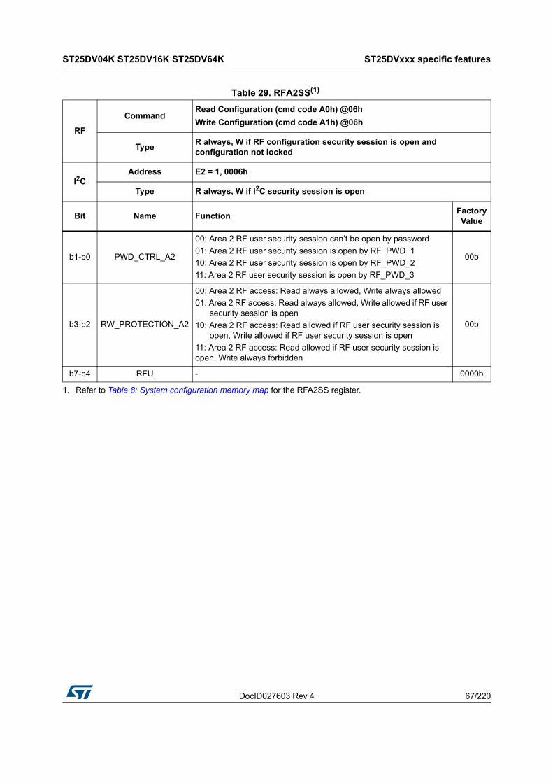
DocID027603 Rev 4 67/220
ST25DV04K ST25DV16K ST25DV64K ST25DVxxx specific features
219
Table 29. RFA2SS(1)
RF
CommandRead Configuration (cmd code A0h) @06h
Write Configuration (cmd code A1h) @06h
TypeR always, W if RF configuration security session is open and configuration not locked
I2CAddress E2 = 1, 0006h
Type R always, W if I2C security session is open
Bit Name FunctionFactory Value
b1-b0 PWD_CTRL_A2
00: Area 2 RF user security session can’t be open by password
01: Area 2 RF user security session is open by RF_PWD_1
10: Area 2 RF user security session is open by RF_PWD_2
11: Area 2 RF user security session is open by RF_PWD_3
00b
b3-b2 RW_PROTECTION_A2
00: Area 2 RF access: Read always allowed, Write always allowed
01: Area 2 RF access: Read always allowed, Write allowed if RF user security session is open
10: Area 2 RF access: Read allowed if RF user security session is open, Write allowed if RF user security session is open
11: Area 2 RF access: Read allowed if RF user security session is open, Write always forbidden
00b
b7-b4 RFU - 0000b
1. Refer to Table 8: System configuration memory map for the RFA2SS register.

ST25DVxxx specific features ST25DV04K ST25DV16K ST25DV64K
68/220 DocID027603 Rev 4
Table 30. RFA3SS(1)
RF
CommandRead Configuration (cmd code A0h) @08h
Write Configuration (cmd code A1h) @08h
TypeR always, W if RF configuration security session is open and configuration not locked
I2CAddress E2 = 1, 0008h
Type R always, W if I2C security session is open
Bit Name FunctionFactory Value
b1-b0 PWD_CTRL_A3
00: Area 3 RF user security session can’t be open by password
01: Area 3 RF user security session is open by RF_PWD_1
10: Area 3 RF user security session is open by RF_PWD_2
11: Area 3 RF user security session is open by RF_PWD_3
00b
b3-b2 RW_PROTECTION_A3
00: Area 3 RF access: Read always allowed / Write always allowed
01: Area 3 RF access: Read always allowed, Write allowed if RF user security session is open
10: Area 3 RF access: Read allowed if RF user security session is open, Write allowed if RF user security session is open
11: Area 3 RF access: Read allowed if RF user security session is open, Write always forbidden
00b
b7-b4 RFU - 0000b
1. Refer to Table 8: System configuration memory map for the RFA3SS register.

DocID027603 Rev 4 69/220
ST25DV04K ST25DV16K ST25DV64K ST25DVxxx specific features
219
Table 31. RFA4SS(1)
RF
CommandRead Configuration (cmd code A0h) @0Ah
Write Configuration (cmd code A1h) @0Ah
TypeR always, W if RF configuration security session is open and configuration not locked
I2CAddress E2 = 1, 000Ah
Type R always, W if I2C security session is open
Bit Name FunctionFactory Value
b1-b0 PWD_CTRL_A4
00: Area 4RF user security session can’t be open by password
01: Area 4 RF user security session is open by RF_PWD_1
10: Area 4 RF user security session is open by RF_PWD_2
11: Area 4 RF user security session is open by RF_PWD_3
00b
b3-b2 RW_PROTECTION_A4
00: Area 4 RF access: Read always allowed, Write always allowed
01: Area 4 RF access: Read always allowed, Write allowed if RF user security session is open
10: Area 4 RF access: Read allowed if RF user security session is open, Write allowed if RF user security session is open
11: Area 4 RF access: Read allowed if RF user security session is open, Write always forbidden
00b
b7-b4 RFU - 0000b
1. Refer to Table 8: System configuration memory map for the RFA4SS register.
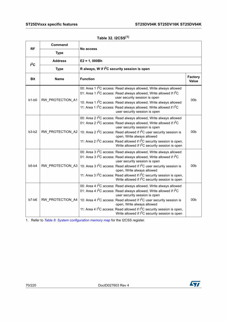
ST25DVxxx specific features ST25DV04K ST25DV16K ST25DV64K
70/220 DocID027603 Rev 4
Table 32. I2CSS(1)
RFCommand
No accessType
I2CAddress E2 = 1, 000Bh
Type R always, W if I2C security session is open
Bit Name FunctionFactory Value
b1-b0 RW_PROTECTION_A1
00: Area 1 I2C access: Read always allowed, Write always allowed
01: Area 1 I2C access: Read always allowed, Write allowed if I2C user security session is open
10: Area 1 I2C access: Read always allowed, Write always allowed
11: Area 1 I2C access: Read always allowed, Write allowed if I2C user security session is open
00b
b3-b2 RW_PROTECTION_A2
00: Area 2 I2C access: Read always allowed, Write always allowed
01: Area 2 I2C access: Read always allowed, Write allowed if I2C user security session is open
10: Area 2 I2C access: Read allowed if I2C user security session is open, Write always allowed
11: Area 2 I2C access: Read allowed if I2C security session is open, Write allowed if I2C security session is open
00b
b5-b4 RW_PROTECTION_A3
00: Area 3 I2C access: Read always allowed, Write always allowed
01: Area 3 I2C access: Read always allowed, Write allowed if I2C user security session is open
10: Area 3 I2C access: Read allowed if I2C user security session is open, Write always allowed
11: Area 3 I2C access: Read allowed if I2C security session is open, Write allowed if I2C security session is open
00b
b7-b6 RW_PROTECTION_A4
00: Area 4 I2C access: Read always allowed, Write always allowed
01: Area 4 I2C access: Read always allowed, Write allowed if I2C user security session is open
10: Area 4 I2C access: Read allowed if I2C user security session is open, Write always allowed
11: Area 4 I2C access: Read allowed if I2C security session is open, Write allowed if I2C security session is open
00b
1. Refer to Table 8: System configuration memory map for the I2CSS register.

DocID027603 Rev 4 71/220
ST25DV04K ST25DV16K ST25DV64K ST25DVxxx specific features
219
Table 33. LOCK_CCFILE(1)
RF
Command
Lock Block (cmd code 22h) @00h/01h
Ext Lock Block (cmd code 32h) @00h/01h
Read Block(2) (cmd code 20h) @00h/01h
Fast Read Block(2) (cmd code C0h) @00h/01h
Ext Read Block(2) (cmd code 30h) @00h/01h
Fast Ext Read Block(2) (cmd code C4h) @00h/01h
Read Multi Block(2) (cmd code 23h) @00h/01h
Ext Read Multi Block(2) (cmd code 33h) @00h/01h
Fast Read Multi Block(2) (cmd code C3h) @00h/01h
Fast Ext Read Multi Block(2) (cmd code C5h) @00h/01h
Get Multi Block SS (cmd code 2Ch) @00h/01h
Ext Get Multi Block SS (cmd code 3Ch) @00h/01h
Type
R always
b0: W if Block 00h is not already locked,
b1: W if Block 01h is not already locked.
I2CAddress E2 = 1, 000Ch
Type R always, W if I2C security session is open
Bit Name FunctionFactory Value
b0 LCKBCK00: Block @ 00h is not Write locked
1: Block @ 00h is Write locked0b
b1 LCKBCK10: Block @ 01h is not Write locked
1: Block @ 01h is Write locked0b
b7-b2 RFU - 000000b
1. Refer to Table 8: System configuration memory map for the LOCK_CCFILE register.
2. With option flag set to 1.

ST25DVxxx specific features ST25DV04K ST25DV16K ST25DV64K
72/220 DocID027603 Rev 4
Table 34. LOCK_CFG(1)
RF
CommandRead Configuration (cmd code A0h) @0Fh
Write Configuration (cmd code A1h) @0Fh
TypeR always, W if RF configuration security session is open and configuration not locked
I2CAddress E2 = 1, 000Fh
Type R always, W if I2C security session is open
Bit Name FunctionFactory Value
b0 LCK_CFG0: Configuration is unlocked
1: Configuration is locked0b
b7-b1 RFU - 0000000b
1. Refer to Table 8: System configuration memory map for the LOCK_CFG register.
Table 35. I2C_PWD(1)
RFCommand
No accessType
I2CAddress E2 = 1, 0900h to 0907h, Present/Write password command format.
Type R if I2C security session is open, W if I2C security session is open
I2C Address
Bit Name FunctionFactory Value
0900h b7-b0
I2C_PWD
Byte 7 (MSB) of password for I2C security session 00h
0901h b7-b0 Byte 6 of password for I2C security session 00h
0902h b7-b0 Byte 5 of password for I2C security session 00h
0903h b7-b0 Byte 4 of password for I2C security session 00h
0904h b7-b0 Byte 3 of password for I2C security session 00h
0905h b7-b0 Byte 2 of password for I2C security session 00h
0906h b7-b0 Byte 1 of password for I2C security session 00h
0907h b7-b0 Byte 0 (LSB) of password for I2C security session 00h
1. Refer to Table 8: System configuration memory map for the I2C_PWD register.

DocID027603 Rev 4 73/220
ST25DV04K ST25DV16K ST25DV64K ST25DVxxx specific features
219
Table 36. RF_PWD_0(1)
RFCommand
Present Password (cmd code B3h)
Write Password (cmd code B1h)
Type WO if RF configuration security session is open
I2CAddress
No accessType
Bit Name FunctionFactory Value
b7-b0
RF_PWD_0
Byte 0 (LSB) of password for RF configuration security session 00h
b7-b0 Byte 1 of password for RF configuration security session 00h
b7-b0 Byte 2 of password for RF configuration security session 00h
b7-b0 Byte 3 of password for RF configuration security session 00h
b7-b0 Byte 4 of password for RF configuration security session 00h
b7-b0 Byte 5 of password for RF configuration security session 00h
b7-b0 Byte 6 of password for RF configuration security session 00h
b7-b0 Byte 7 (MSB) of password for RF configuration security session 00h
1. Refer to Table 8: System configuration memory map for the RF_PWD_0 register.
Table 37. RF_PWD_1(1)
RF CommandPresent Password (cmd code B3h)
Write Password (cmd code B1h)
Type WO if RF configuration security session is open with RF password 1
I2C AddressNo access
Type
Bit Name FunctionFactory Value
b7-b0
RF_PWD_1
Byte 0 (LSB) of password 1 for RF user security session 00h
b7-b0 Byte 1 of password 1 for RF user security session 00h
b7-b0 Byte 2 of password 1 for RF user security session 00h
b7-b0 Byte 3 of password 1 for RF user security session 00h
b7-b0 Byte 4 of password 1 for RF user security session 00h
b7-b0 Byte 5 of password 1 for RF user security session 00h
b7-b0 Byte 6 of password 1 for RF user security session 00h
b7-b0 Byte 7 (MSB) of password 1 for RF user security session 00h
1. Refer to Table 8: System configuration memory map for the RF_PWD_1 register.

ST25DVxxx specific features ST25DV04K ST25DV16K ST25DV64K
74/220 DocID027603 Rev 4
Table 38. RF_PWD_2(1)
RFCommand
Present Password (cmd code B3h)
Write Password (cmd code B1h)
Type WO if RF user security session is open with RF password 2
I2CAddress
No accessType
Bit Name FunctionFactory Value
b7-b0
RF_PWD_2
Byte 0 (LSB) of password 2 for RF user security session 00h
b7-b0 Byte 1 of password 2 for RF user security session 00h
b7-b0 Byte 2 of password 2 for RF user security session 00h
b7-b0 Byte 3 of password 2 for RF user security session 00h
b7-b0 Byte 4 of password 2 for RF user security session 00h
b7-b0 Byte 5 of password 2 for RF user security session 00h
b7-b0 Byte 6 of password 2 for RF user security session 00h
b7-b0 Byte 7 (MSB) of password 2 for RF user security session 00h
1. Refer to Table 8: System configuration memory map for the RF_PWD_2 register.
Table 39. RF_PWD_3(1)
RFCommand
Present Password (cmd code B3h)
Write Password (cmd code B1h)
Type WO if RF user security session is open with RF password 3
I2CAddress
No accessType
Bit Name FunctionFactory Value
b7-b0
RF_PWD_3
Byte 0 (LSB) of password 3for RF user security session 00h
b7-b0 Byte 1 of password 3 for RF user security session 00h
b7-b0 Byte 2 of password 3 for RF user security session 00h
b7-b0 Byte 3 of password 3 for RF user security session 00h
b7-b0 Byte 4 of password 3 for RF user security session 00h
b7-b0 Byte 5 of password 3 for RF user security session 00h
b7-b0 Byte 6 of password 3 for RF user security session 00h
b7-b0 Byte 7 (MSB) of password 3 for RF user security session 00h
1. Refer to Table 8: System configuration memory map for the RF_PWD_3 register.

DocID027603 Rev 4 75/220
ST25DV04K ST25DV16K ST25DV64K ST25DVxxx specific features
219
5.6.2 Passwords and security sessions
ST25DVxxx provides protection of user memory and system configuration static registers. RF user and I2C host can access those protected data by opening security sessions with the help of passwords. Access rights is more restricted when security sessions are closed, and less restricted when security sessions are open.
Dynamic registers and fast transfer mode mailbox are not protected by any security session.
There is three type of security sessions, as shown in Table 41:
All passwords are 64-bits long, and default factory passwords value is 0000000000000000h.
The ST25DVxxx passwords management is organized around RF and I2C dedicated set of commands to access the dedicated registers in system configuration area where password values are stored.
Table 40. I2C_SSO_Dyn(1)
RFCommand
No accessType
I2CAddress E2 = 0, 2004h
Type RO
Bit Name FunctionFactory Value
b0 I2C_SSO
0: I2C security session close
1: I2C security session open
(Set or reset via I2C Present password command)
0b
b7-b1 RFU - 0b
1. Refer to Table 9: Dynamic registers memory map for the I2C_SS0_Dyn register.
Table 41. Security session type
Security session
Open by presenting Right granted when security session is open, and until it is closed
RF user
RF password 1, 2 or 3(1)
(RF_PWD_1, RF_PWD_2, RF_PWD_3)
RF user access to protected user memory as defined in RFAiSS registers
RF user write access to RF password 1, 2 or 3(2)
RF configuration
RF password 0(RF_PWD_0)
RF user write access to configuration static registers RF user write access to RF password 0
I2CI2C password(I2C_PWD)
I2C host access to protected user memory as defined in I2CSS register
I2C host write access to configuration static registers I2C host write access to I2C password
1. Password number must be the same as the one selected for protection.
2. Write access to the password number corresponding to the password number presented.

ST25DVxxx specific features ST25DV04K ST25DV16K ST25DV64K
76/220 DocID027603 Rev 4
The dedicated password commands in RF mode are:
• Write Password command (code B1h): see Section 7.6.35: Write Password.
• Present Password command (code B3h): see Section 7.6.36: Present Password.
RF user possible actions for security sessions are:
• Open RF user security session: Present Password command, with password number 1, 2 or 3 and the valid corresponding password
• Write RF password: Present Password command, with password number (0, 1, 2 or 3) and the current valid corresponding password. Then Write Password command, with same password number (0, 1, 2 or 3) and the new corresponding password.
• Close RF user security session: Present Password command, with a different password number than the one used to open session or any wrong password. Or remove tag from RF field (POR).
• Open RF configuration security session: Present Password command, with password number 0 and the valid password 0.
• Close RF configuration security session: Present Password command, with a password number different than 0, or password number 0 and wrong password 0. Or remove tag from RF field (POR).
Opening any new RF security session (user or configuration) automatically close the previously open one (even if it fails).
There is no interaction between I2C and RF security sessions. Both are independent, and can run in parallel.
Caution: If ST25DVxxx is powered through VCC, removing VCC or setting LPD high during a RF command can abort the command. As a consequence, before writing a new password, RF user should check if VCC is ON, by reading EH_CTRL_Dyn register bit 3 (VCC_ON), and eventually ask host to maintain or to shut down VCC, and not change voltage applied on LPD while issuing the Write Password command in order to avoid password corruption.

DocID027603 Rev 4 77/220
ST25DV04K ST25DV16K ST25DV64K ST25DVxxx specific features
219
Figure 22. RF security sessions management
The dedicated password commands in I2C mode are:
• I2C Write Password command: see Section 6.6.2: I2C write password command description.
• I2C Present Password command: see Section 6.6.2: I2C write password command description.
I2C host possible actions for security sessions are:
• Open I2C security session: I2C Present Password command with valid I2C password.
• Write I2C password: I2C Present Password command with valid I2C password. Then I2C Write Password command with new I2C password.
• Close I2C security session: I2C Present Password command with wrong I2C password. Or remove tag VCC power supply (POR).
• Check if I2C security session is open: I2C host can read the current status (open or closed) of I2C security session by reading the I2C_SSO_Dyn register.

ST25DVxxx specific features ST25DV04K ST25DV16K ST25DV64K
78/220 DocID027603 Rev 4
There is no interaction between I2C and RF security sessions. Both are independent and can run in parallel.
Figure 23. I2C security sessions management
5.6.3 User memory protection
On factory delivery, areas are not protected.
Each area can be individually protected in read and/or write access from RF and I2C.
Area 1 is always readable (from RF and I2C).
Furthermore, RF blocks 0 and 1 (I2C bytes 0000h to 00007h) can be independently write locked.
User memory protection from RF access
In RF mode, each memory area of the ST25DVxxx can be individually protected by one out of three available passwords (RF password 1, 2 or 3), and each area can also have individual Read/Write access conditions.
For each area, an RFAiSS register is used to:
• Select the RF password that unlock the RF user security session for this area
• Select the protection against read and write operations for this area
(See Table 28: RFA1SS, Table 29: RFA2SS, Table 30: RFA3SS and Table 31: RFA4SS for details about available read and write protections).

DocID027603 Rev 4 79/220
ST25DV04K ST25DV16K ST25DV64K ST25DVxxx specific features
219
Note: Setting 00b in PWD_CTRL_Ai field means that RF user security session cannot be open by any password for the corresponding area.
When updating RFAiSS registers, the new protection value is effective immediately after the register write completion.
• Rf blocks 0 and 1 are exceptions to this protection mechanism:
– RF blocks 0 and 1 can be individually write locked by issuing a (Ext) Lock Single Block RF command. Once locked, they cannot be unlock through RF. LOCK_CCFILE register is automatically updated when using (Ext) Lock Single Block command.
– A RF user needs no password to lock blocks 0 and/or 1.
– Locking blocks 0 and/or 1 is possible even if the configuration is locked (LOCK_CFG=1).
– Locking blocks 0 and/or 1 is possible even if the area is write locked.
– Unlocking area1 (through RFA1SS register) does not unlock blocks 0 and 1 if they have been locked though (Ext) Lock Block command.
– Once locked, the RF user cannot unlock blocks 0 and/or 1 (can be done by I2C host).
Note: When areas size are modified (ENDAi registers), RFAiSS registers are not modified.
User memory protection from I2C access
In I2C mode, each area can also have individual Read/Write access conditions, but only one I2C password is used to unlock I2C security session for all areas.
The I2CSS register is used to set protection against read and write operation for each area (see Table 32: I2CSS for details about available read and write protections).
When updating I2CSS registers, the new protection value is effective immediately after the register write completion.
I2C user memory Bytes 0000h to 0003h (RF Block 0) and 0004h to 0007h (RF Block 1) can be individually locked and unlocked by writing in the LOCK_CCFILE register (by group of 4 Bytes), independently of Area 1 protection. Unlocking Area 1 (through I2CSS register) does not unlock those bytes if they have been locked though the LOCK_CCFILE register.
Note: When areas size are modified (ENDAi registers), I2CSS register is not modified.
Retrieve the security status of a user memory block or byte
RF user can read a block security status by issuing following RF commands:
• (Ext) Get Multiple Blocks Security Status command.
• (Ext) (Fast) Read Single Block with option flag set to 1.
• (Ext) (Fast) Read Multiple Blocks with option flag set to 1.
ST25DV will respond with a Block security status containing a Lock_bit flag as specified in ISO 15693 standard. This lock_bit flag is set to one if block is locked against write.
Lock_bit flag value may vary if corresponding RF user security session is open or closed.
I2C host can retrieve a block security status by reading the I2CSS register to get security status of the corresponding area and by reading the I2C_SSO_Dyn register to know if I2C security session is open or closed.

ST25DVxxx specific features ST25DV04K ST25DV16K ST25DV64K
80/220 DocID027603 Rev 4
For blocks 0 and 1 (Bytes 0000h to 0007h in I2C user memory), lock status can also be read in the LOCK_CCFILE register.
5.6.4 System memory protection
By default, system memory (static registers) is write protected, both in RF and I2C.
I2C host must open the I2C security session (by presenting a valid I2C password) to enable write access to system configuration static registers.
I2C host doesn’t have read or write access to RF passwords.
By default, I2C host can read all system configuration static registers (except RF passwords)
In RF, to enable write access to system configuration static registers, RF user must open the RF configuration security session (by presenting a valid RF password 0) and system configuration must not be locked (LOCK_CFG=00h).
RF doesn’t have read or write access to I2C password.
By default, RF user can read all system configuration static registers, except all passwords, LOCK_CCFILE, LOCK_DSFID and LOCK_AFI.
RF configuration lock:
• RF write access to system configuration static registers can be locked by writing 01h in the LOCK_CFG register (by RF or I2C).
• RF user cannot unlock system configuration if LOCK_CFG=01h, even after opening RF configuration security session (only I2C host can unlock system configuration).
• When system configuration is locked (LOCK_CFG=01h), it is still possible to change RF passwords (0 to 3).
Device identification registers:
• AFI and DFSID registers can be independently locked by RF user, issuing respectively a Lock AFI and a Lock DSFID command. Lock is definitive: once locked, AFI and DSFID registers cannot be unlocked (either by RF or I2C). System configuration locking mechanism (LOCK_CFG=01h) does not lock AFI and DSFID registers.
• Other device identification registers (MEM_SIZE, BLK_SIZE, IC_REF, UID, IC_REV) are read only registers for both RF and I2C.

DocID027603 Rev 4 81/220
ST25DV04K ST25DV16K ST25DV64K ST25DVxxx specific features
219
5.7 Device Parameter Registers
Table 42. LOCK_DSFID(1)
RFCommand Lock DSFID (cmd code 2Ah)
Type WO if DSFID not locked
I2CAddress E2 = 1, 0010h
Type RO
Bit Name FunctionFactory Value
b0 LOCK_DSFID0: DSFID is not locked
1: DSFID is locked0b
b7-b1 RFU - 0000000b
1. Refer to Table 8: System configuration memory map for the LOCK_DSFID register.
Table 43. LOCK_AFI(1)
RFCommand Lock AFI (cmd code 28h)
Type WO if AFI not locked
I2CAddress E2 = 1, 0011h
Type RO
Bit Name FunctionFactory Value
b0 LOCK_AFI0: AFI is not locked
1: AFI is locked0b
b7-b1 RFU - 0000000b
1. Refer to Table 8: System configuration memory map for the LOCK_AFI register.
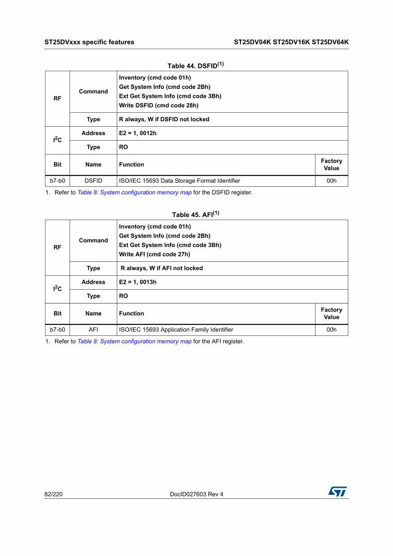
ST25DVxxx specific features ST25DV04K ST25DV16K ST25DV64K
82/220 DocID027603 Rev 4
Table 44. DSFID(1)
RFCommand
Inventory (cmd code 01h)
Get System Info (cmd code 2Bh)
Ext Get System Info (cmd code 3Bh)
Write DSFID (cmd code 28h)
Type R always, W if DSFID not locked
I2CAddress E2 = 1, 0012h
Type RO
Bit Name FunctionFactory Value
b7-b0 DSFID ISO/IEC 15693 Data Storage Format Identifier 00h
1. Refer to Table 8: System configuration memory map for the DSFID register.
Table 45. AFI(1)
RFCommand
Inventory (cmd code 01h)
Get System Info (cmd code 2Bh)
Ext Get System Info (cmd code 3Bh)
Write AFI (cmd code 27h)
Type R always, W if AFI not locked
I2CAddress E2 = 1, 0013h
Type RO
Bit Name FunctionFactory Value
b7-b0 AFI ISO/IEC 15693 Application Family Identifier 00h
1. Refer to Table 8: System configuration memory map for the AFI register.

DocID027603 Rev 4 83/220
ST25DV04K ST25DV16K ST25DV64K ST25DVxxx specific features
219
Table 46. MEM_SIZE(1)
RFCommand
Get System Info(2) (cmd code 2Bh)
Ext Get System Info (cmd code 3Bh)
Type RO
I2CAddress E2=1, 0014h to 0015h
Type RO
I2C Address
Bit Name Function Factory Value
0014h b7-b0
MEM_SIZE
Address 0015h: LSB byte of the memory size expressed in RF blocks
ST25DV04K-XX: 7FhST25DV16K-XX: FFhST25DV64K-XX: FFh
0015h b7-b0Address 0014h: MSB byte of the memory size expressed in RF blocks
ST25DV04K-XX: 00hST25DV16K-XX: 01hST25DV64K-XX: 07h
1. Refer to Table 8: System configuration memory map for the MEM_SIZE register.
2. Only ST25DV04K-IE and ST25DV04K-JF
Table 47. BLK_SIZE(1)
RFCommand
Get System Info(2) (cmd code 2Bh)
Ext Get System Info (cmd code 3Bh)
Type RO
I2CAddress E2 = 1, 0016h
Type RO
Bit Name FunctionFactory Value
b7-b0 BLK_SIZE RF user memory block size 03h
1. Refer to Table 8: System configuration memory map for the BLK_SIZE register.
2. Only ST25DV04K-IE and ST25DV04K-JF

ST25DVxxx specific features ST25DV04K ST25DV16K ST25DV64K
84/220 DocID027603 Rev 4
Table 48. IC_REF(1)
RFCommand
Get System Info (cmd code 2Bh)
Ext Get System Info (cmd code 3Bh)
Type RO
I2CAddress E2 = 1, 0017h
Type RO
Bit Name Function Factory Value
b7-b0 IC_REF ISO/IEC 15693 IC Reference
ST25DV04K-IE: 24hST25DV16K-IE: 26hST25DV64K-IE: 26hST25DV04K-JF: 24hST25DV16K-JF: 26hST25DV64K-JF: 26h
1. Refer to Table 8: System configuration memory map for the IC_REF register.
Table 49. UID(1)
RFCommand
Inventory (cmd code 01h) Get System Info (cmd code 2Bh) Ext Get System Info (cmd code 3Bh)
Type RO
I2CAddress E2=1, 0018h to 001Fh
Type RO
I2C Address
Bit Name Function Factory Value
0018h b7-b0
UID
ISO/IEC 15693 UID byte 0 (LSB)
IC manufacturer serial number
0019h b7-b0 ISO/IEC 15693 UID byte 1
001Ah b7-b0 ISO/IEC 15693 UID byte 2
001Bh b7-b0 ISO/IEC 15693 UID byte 3
001Ch b7-b0 ISO/IEC 15693 UID byte 4
001Dh b7-b0 ISO/IEC 15693 UID byte 5: ST Product code
ST25DV04K-IE: 24hST25DV16K-IE: 26hST25DV64K-IE: 26hST25DV04K-JF: 25hST25DV16K-JF: 27hST25DV64K-JF: 27h
001Eh b7-b0 ISO/IEC 15693 UID byte 6: IC Mfg code 02h
001Fh b7-b0 ISO/IEC 15693 UID byte 7 (MSB) E0h
1. Refer to Table 8: System configuration memory map for the UID register.

DocID027603 Rev 4 85/220
ST25DV04K ST25DV16K ST25DV64K ST25DVxxx specific features
219
Table 50. IC_REV(1)
1. Refer to Table 8: System configuration memory map for the IC_REV register.
RFCommand
No accessType
I2CAddress E2 = 1, 0020h
Type RO
Bit Name Function Factory Value
b7-b0 IC_REV IC revision Depending on revision

I2C operation ST25DV04K ST25DV16K ST25DV64K
86/220 DocID027603 Rev 4
6 I2C operation
6.1 I2C protocol
The device supports the I2C protocol. This is summarized in Figure 24: I2C bus protocol. Any device that sends data to the bus is defined as a transmitter, and any device that reads data is defined as a receiver. The device that controls the data transfer is known as the bus master, and the other as the slave device. A data transfer can only be initiated by the bus master, which also provides the serial clock for synchronization. The ST25DVxxx device is a slave in all communications.
Figure 24. I2C bus protocol
6.1.1 Start condition
Start is identified by a falling edge of serial data (SDA) while the serial clock (SCL) is stable in the high state. A Start condition must precede any data transfer command. The device continuously monitors (except during a write cycle) the SDA and the SCL for a Start condition, and does not respond unless one is given.

DocID027603 Rev 4 87/220
ST25DV04K ST25DV16K ST25DV64K I2C operation
219
6.1.2 Stop condition
Stop is identified by a rising edge of serial data (SDA) while the serial clock (SCL) is stable and driven high. A Stop condition terminates communication between the device and the bus master. A Read command that is followed by NoAck can be followed by a Stop condition to force the device into the Standby mode. A Stop condition at the end of a Write command triggers the internal write cycle.
6.1.3 Acknowledge bit (ACK)
The acknowledge bit is used to indicate a successful byte transfer. The bus transmitter, whether a bus master or a slave device, releases the serial data (SDA) after sending eight bits of data. During the 9th clock pulse period, the receiver pulls the SDA low to acknowledge the receipt of the eight data bits.
6.1.4 Data input
During data input, the device samples serial data (SDA) on the rising edge of the serial clock (SCL). For correct device operation, the SDA must be stable during the rising edge of the SCL, and the SDA signal must change only when the SCL is driven low.
6.2 I2C timeout
During the execution of an I²C operation, RF communications are not possible.
To prevent RF communication freezing due to inadvertent unterminated instructions sent to the I²C bus, the ST25DVxxx features a timeout mechanism that automatically resets the I²C logic block.
6.2.1 I2C timeout on Start condition
I2C communication with the ST25DVxxx starts with a valid Start condition, followed by a device select code.
If the delay between the Start condition and the following rising edge of the Serial Clock (SCL) that samples the most significant of the Device Select exceeds the tSTART_OUT time (see Table 209: I2C AC characteristics up to 85°C and Table 210: I2C AC characteristics up to 125°C), the I²C logic block is reset and further incoming data transfer is ignored until the next valid Start condition.
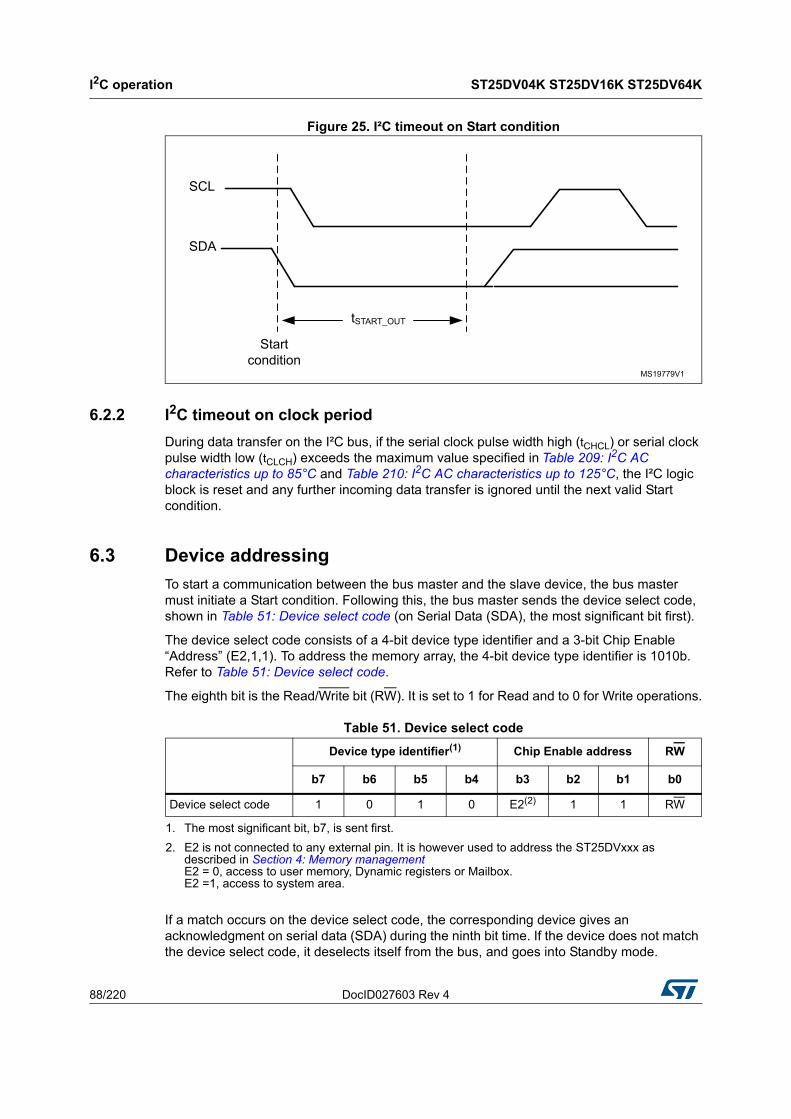
I2C operation ST25DV04K ST25DV16K ST25DV64K
88/220 DocID027603 Rev 4
Figure 25. I²C timeout on Start condition
6.2.2 I2C timeout on clock period
During data transfer on the I²C bus, if the serial clock pulse width high (tCHCL) or serial clock pulse width low (tCLCH) exceeds the maximum value specified in Table 209: I2C AC characteristics up to 85°C and Table 210: I2C AC characteristics up to 125°C, the I²C logic block is reset and any further incoming data transfer is ignored until the next valid Start condition.
6.3 Device addressing
To start a communication between the bus master and the slave device, the bus master must initiate a Start condition. Following this, the bus master sends the device select code, shown in Table 51: Device select code (on Serial Data (SDA), the most significant bit first).
The device select code consists of a 4-bit device type identifier and a 3-bit Chip Enable “Address” (E2,1,1). To address the memory array, the 4-bit device type identifier is 1010b. Refer to Table 51: Device select code.
The eighth bit is the Read/Write bit (RW). It is set to 1 for Read and to 0 for Write operations.
If a match occurs on the device select code, the corresponding device gives an acknowledgment on serial data (SDA) during the ninth bit time. If the device does not match the device select code, it deselects itself from the bus, and goes into Standby mode.
Table 51. Device select code
Device type identifier(1)
1. The most significant bit, b7, is sent first.
Chip Enable address RW
b7 b6 b5 b4 b3 b2 b1 b0
Device select code 1 0 1 0 E2(2)
2. E2 is not connected to any external pin. It is however used to address the ST25DVxxx as described in Section 4: Memory management E2 = 0, access to user memory, Dynamic registers or Mailbox. E2 =1, access to system area.
1 1 RW

DocID027603 Rev 4 89/220
ST25DV04K ST25DV16K ST25DV64K I2C operation
219
6.4 I2C Write operations
Following a Start condition, the bus master sends a device select code with the Read/Write bit (RW) reset to 0. The device acknowledges this, and waits for two address bytes. The device responds to each address byte with an acknowledge bit, and then waits for the data byte.
Each data byte in the memory has a 16-bit (two-byte wide) address. The most significant byte (see Table 53: Address most significant byte) is sent first, followed by the least significant byte (see Table 54: Address least significant byte). Bits b15 to b0 form the address of the byte in memory.
When the bus master generates a Stop condition immediately after the Ack bit (in the tenth-bit time slot), either at the end of a byte write or a sequential write, the internal write cycle is triggered. A Stop condition at any other time slot does not trigger the internal write cycle.
After the Stop condition, the delay tW, and the successful completion of a Write operation, the device’s internal address counter is incremented automatically, to point to the next byte address after the last one that was modified.
After an unsuccessful write operation, ST25DVxxx enters in I2C dead state: internal address counter is not incremented, and ST25DVxxx is waiting for a full new I2C instruction.
During the internal write cycle, the serial data (SDA) signal is disabled internally, and the device does not respond to any requests.
Caution: I2C Writing data in user or system memory (EEPROM), transit via the 256-Bytes fast transfer mode's buffer. Consequently fast transfer mode must be deactivated before starting any write operation in user or system memory, otherwise command will be NotACK, programming is not done and device goes in standby mode.
Table 52. Operating modes
Mode RW bit Bytes Initial sequence
Current address read 1 1 Start, device select, RW = 1
Random address read0
1Start, device select, RW = 0, address
1 reStart, device select, RW = 1
Sequential read 1 ≥ 1 Similar to current or random address read
Byte write 0 1 Start, device select, RW = 0
Sequential write 0 ≤ 256 byte Start, device select, RW = 0
Table 53. Address most significant byte
b15 b14 b13 b12 b11 b10 b9 b8
Table 54. Address least significant byte
b7 b6 b5 b4 b3 b2 b1 b0

I2C operation ST25DV04K ST25DV16K ST25DV64K
90/220 DocID027603 Rev 4
6.4.1 I2C Byte write
After the device select code and the address bytes, the bus master sends one data byte.
If byte write is not inhibited, the device replies with Ack.
If byte write is inhibited, the device replies with NoAck.
The bus master terminates the transfer by generating a Stop condition (see Figure 26: Write mode sequences when write is not inhibited).
For byte write in EEPROM (user memory or system configuration), internal programming starts after the Ack, for a duration of tW (as defined in Table 209: I2C AC characteristics up to 85°C and Table 210: I2C AC characteristics up to 125°C).
For writes in fast transfer mode buffer or Dynamic registers, internal programming is done at the Ack.
If byte write is inhibited, the device replies with NoAck. The bus master terminates the transfer by generating a Stop condition and byte location not is modified (see Figure 27: Write mode sequences when write is inhibited).
Byte write is inhibited if byte complies with one of the following conditions:
• Byte is in user memory and is write protected with LOCK_CCFILE register.
• Byte is in user memory and is write protected with I2CSS register, and I2C security session is closed.
• Byte is in user memory and fast transfer mode is activated.
• Byte is in system memory and is a Read Only register.
• Byte is in system memory and I2C security session is closed.
• Byte is in fast transfer mode’s mailbox and is not the first Byte of mailbox.
• Byte is in fast transfer mode’s mailbox and mailbox is busy.
• Byte is in fast transfer mode’s mailbox and fast transfer mode is not activated.
• Byte is in dynamic registers area and is a Read Only register.
6.4.2 I2C Sequential write
The I2C sequential write allows up to 256 bytes to be written in one command, provided they are all located in the same user memory area or are all located in writable addresses.
After each byte is transferred, the internal byte address counter is incremented.
For each byte sent by the bus master:
• If byte write is not inhibited, the device replies with Ack.
• If byte write is inhibited, the device replies with NoAck.
The transfer is terminated by the bus master generating a Stop condition:
• For writes in EEPROM (user memory or system configuration), if all bytes have been Ack'ed, internal programming of all bytes starts after the last Ack, for a duration dependent on the number of bytes to write (see below).
• For writes in fast transfer mode buffer or Dynamic registers, if all bytes have been Ack'ed, internal programming is done at the Ack.
• If some bytes have been NotAck’ed, no internal programming is done (0 byte written).

DocID027603 Rev 4 91/220
ST25DV04K ST25DV16K ST25DV64K I2C operation
219
Byte write is inhibited if byte complies with conditions described in Section 6.4.1: I2C Byte write, in addition:
• Byte is in user memory but does not belong to same area than previous received byte (area border crossing is forbidden).
• 256 write occurrence have already been reached in the same sequential write.
EEPROM memory (user memory and system configuration) is internally organized in pages of 4 bytes long. Data located in a same page all share the same most significant memory address bits b16-b2.
I2C sequential write programming time in the EEPROM memory is dependent on this internal organization: total programming time is the I2C write time tW (as defined in Table 209: I2C AC characteristics up to 85°C and Table 210: I2C AC characteristics up to 125°C) multiplied by the number of internal EEPROM pages where the data must be programmed, including incomplete pages. For example, a 256 Bytes I2C sequential write, starting at address 0002h will write data over 65 pages. Total write time in this case is tW x 65.
Figure 26. Write mode sequences when write is not inhibited
Note: N ≤ 256

I2C operation ST25DV04K ST25DV16K ST25DV64K
92/220 DocID027603 Rev 4
Figure 27. Write mode sequences when write is inhibited
Note: N ≤ 256
6.4.3 Minimizing system delays by polling on ACK
During the internal write cycle, the device disconnects itself from the bus, and writes a copy of the data from its internal latches to the memory cells. The maximum I²C write time (tw) is shown in Table 209: I2C AC characteristics up to 85°C and Table 210: I2C AC characteristics up to 125°C, but the typical time is shorter. To make use of this, a polling sequence can be used by the bus master.
The sequence, as shown in Figure 28: Write cycle polling flowchart using ACK, is:
• Initial condition: a write cycle is in progress.
• Step 1: the bus master issues a Start condition followed by a device select code (the first byte of the new instruction).
• Step 2: if the device is busy with the internal write cycle, no Ack is returned and the bus master goes back to Step 1. If the device has terminated the internal write cycle, it responds with an Ack, indicating that the device is ready to receive the second part of the instruction (the first byte of this instruction having been sent during Step 1).
Note: There is no need of polling when writing in dynamic registers or in mailbox, since programming time is null.

DocID027603 Rev 4 93/220
ST25DV04K ST25DV16K ST25DV64K I2C operation
219
Figure 28. Write cycle polling flowchart using ACK

I2C operation ST25DV04K ST25DV16K ST25DV64K
94/220 DocID027603 Rev 4
6.5 I2C read operations
Read operation in user memory is performed successfully only if:
• Area to which the byte belongs is not read protected by I2CSS register.
• Area to which the byte belongs is read protected by I2CSS register, but I2C security session is open.
Read operations in system memory and dynamic registers are done independently of any protection mechanism, except I2C_PWD register which needs I2C security session to be open first.
Read operation in fast transfer mode’s mailbox is performed successfully only if fast transfer mode is activated.
If read is not successful, ST25DVxxx releases the bus and I2C host reads byte value FFh.
After the successful completion of a read operation, the device’s internal address counter is incremented by one, to point to the next byte address.
After an unsuccessful read operation, ST25DVxxx enters in I2C dead state: internal address counter is not incremented, and ST25DVxxx is waiting for a full new I2C instruction.
6.5.1 Random Address Read
A dummy write is first performed to load the address into this address counter (as shown in Figure 29: Read mode sequences) but without sending a Stop condition. Then, the bus master sends another Start condition, and repeats the device select code, with the Read/Write bit (RW) set to 1. The device acknowledges this, and outputs the contents of the addressed byte. The bus master must not acknowledge the byte, and terminates the transfer with a Stop condition.
6.5.2 Current Address Read
For the Current Address Read operation, following a Start condition, the bus master only sends a device select code with the Read/Write bit (RW) set to 1. The device acknowledges this, and outputs the byte addressed by the internal address counter. The counter is then incremented. The bus master terminates the transfer with a Stop condition, as shown in Figure 29: Read mode sequences, without acknowledging the byte.

DocID027603 Rev 4 95/220
ST25DV04K ST25DV16K ST25DV64K I2C operation
219
Figure 29. Read mode sequences
6.5.3 Sequential Read access
This operation can be used after a Current Address Read or a Random Address Read. The bus master does acknowledge the data byte output, and sends additional clock pulses so that the device continues to output the next byte in sequence. To terminate the stream of bytes, the bus master must not acknowledge the last byte, and must generate a Stop condition, as shown in Figure 29: Read mode sequences.
The output data comes from consecutive addresses, with the internal address counter automatically incremented after each byte output.
Sequential read in user memory:
• Sequential read cannot cross area borders. After reaching area border, device continues to output FFh
• There is no roll over inside area or at the end of user memory (ST25DVxxx returns only FFh after last user memory byte address).
I2C operation ST25DV04K ST25DV16K ST25DV64K
96/220 DocID027603 Rev 4
Sequential read in system memory:
• There is no roll over after reaching end of system memory (ST25DV returns only FFh after last system memory byte address).
• Sequential read in dynamic registers:
• It is possible to read sequentially dynamic registers and fast transfer mode’s mailbox (contiguous I2C addresses).
Sequential read in dynamic registers:
• There is no roll over at the end of the mailbox (ST25DV returns only FFh after last system memory byte address).
6.5.4 Acknowledge in Read mode
For all Read commands, the device waits, after each byte read, for an acknowledgment during the ninth bit time. If the bus master does not drive Serial Data (SDA) low during this time, the device terminates the data transfer and switches to its Standby mode.

DocID027603 Rev 4 97/220
ST25DV04K ST25DV16K ST25DV64K I2C operation
219
6.6 I2C password management
The ST25DVxxx controls I2C security session using an I2C 64-bit password. This I2C password is managed with two I2C dedicated commands: I2C present password and I2C write password.
6.6.1 I2C present password command description
The I2C present password command is used in I2C mode to present the password to the ST25DVxxx. This is used to open I2C security session or to allow I2C password modification (see Section 5.6: Data Protection for detailed explanation about password usage).
Following a Start condition, the bus master sends a device select code with the Read/Write bit (RW) reset to 0 and the Chip Enable bit E2 at 1. The device acknowledges this, as shown in Figure 30: I2C Present Password Sequence, and waits for two I2C password address bytes, 09h and 00h. The device responds to each address byte with an acknowledge bit, and then waits for the eight password data bytes, the validation code, 09h, and a resend of the eight password data bytes. The most significant byte of the password is sent first, followed by the least significant bytes.
It is necessary to send the 64-bit password twice to prevent any data corruption during the sequence. If the two 64-bit passwords sent are not exactly the same, the ST25DVxxx does not start the internal comparison.
When the bus master generates a Stop condition immediately after the Ack bit (during the tenth bit time slot), an internal delay equivalent to the write cycle time is triggered. A Stop condition at any other time does not trigger the internal delay. During that delay, the ST25DVxxx compares the 64 received data bits with the 64 bits of the stored I2C password. If the values match, the I2C security session is open after the internal delay, and the I2C_SSO_Dyn register is set to 01h. If the values do not match, the I2C security session is closed and I2C_SSO_dyn register is set to 00h.
During the internal delay, the serial data (SDA) signal is disabled internally, and the device does not respond to any requests.
I2C_SSO_Dyn is a Dynamic register, it can be checked via I2C host to know If I2C security session is open.
Figure 30. I2C Present Password Sequence

I2C operation ST25DV04K ST25DV16K ST25DV64K
98/220 DocID027603 Rev 4
6.6.2 I2C write password command description
The I2C write password command is used to update the I2C password value (register I2C_PWD). It cannot be used to update any of the RF passwords. After the write cycle, the new I2C password value is automatically activated. The I2C password value can only be modified after issuing a valid I2C present password command.
Following a Start condition, the bus master sends a device select code with the Read/Write bit (RW) reset to 0 and the Chip Enable bit E2 at 1. The device acknowledges this, as shown in Figure 31: I2C Write Password Sequence, and waits for the two I2C password address bytes, 09h and 00h. The device responds to each address byte with an acknowledge bit, and then waits for the four password data bytes, the validation code, 07h, and a resend of the eight password data bytes. The most significant byte of the password is sent first, followed by the least significant bytes.
It is necessary to send twice the 64-bit password to prevent any data corruption during the write sequence. If the two 64-bit passwords sent are not exactly the same, the ST25DVxxx does not modify the I2C password value.
When the bus master generates a Stop condition immediately after the Ack bit (during the tenth bit time slot), the internal write cycle is triggered. A Stop condition at any other time does not trigger the internal write cycle.
During the internal write cycle, the serial data (SDA) signal is disabled internally, and the device does not respond to any requests.
Caution: I2C write password command data transits via the 256-Bytes fast transfer mode's buffer. Consequently fast transfer mode must be deactivated before issuing a write password command, otherwise command is NotACK (after address LSB), and programming is not done and device goes in standby mode.
Figure 31. I2C Write Password Sequence

DocID027603 Rev 4 99/220
ST25DV04K ST25DV16K ST25DV64K RF operations
219
7 RF operations
Contactless exchanges are performed in RF mode as specified by ISO/IEC 15693 or NFC Forum Type 5. The ST25DVxxx communicates via the 13.56 MHz carrier electromagnetic wave on which incoming data are demodulated from the received signal amplitude modulation (ASK: amplitude shift keying). The received ASK wave is 10% or 100% modulated with a data rate of 1.6 Kbit/s using the 1/256 pulse coding mode or a data rate of 26 Kbit/s using the 1/4 pulse coding mode.
Outgoing data are generated by the ST25DVxxx load variation using Manchester coding with one or two subcarrier frequencies at 423 kHz and 484 kHz. Data are transferred from the ST25DVxxx at 6.6 Kbit/s in low data rate mode and 26 Kbit/s in high data rate mode. The ST25DVxxx supports the 53 Kbit/s in high data rate mode in one subcarrier frequency at 423 kHz.
The ST25DVxxx follows ISO/IEC 15693 or NFC Forum Type 5 recommendation for radio-frequency power and signal interface and for anticollision and transmission protocol.
7.1 RF communication
7.1.1 Access to a ISO/IEC 15693 device
The dialog between the “RF reader” and the ST25DVxxx takes place as follows:
These operations use the RF power transfer and communication signal interface described below (see Power transfer, Frequency and Operating field). This technique is called RTF (Reader talk first).
• activation of the ST25DVxxx by the RF operating field of the reader,
• transmission of a command by the reader (ST25DVxxx detects carrier amplitude modulation)
• transmission of a response by the ST25DVxxx(ST25DVxxx modulates is load clocked at subcarrier rate)
Operating field
The ST25DVxxx operates continuously between the minimum and maximum values of the electromagnetic field H defined in Table 214: RF characteristics. The Reader has to generate a field within these limits.
Power transfer
Power is transferred to the ST25DVxxx by radio frequency at 13.56 MHz via coupling antennas in the ST25DVxxx and the Reader. The RF operating field of the reader is transformed on the ST25DVxxx antenna to an AC voltage which is rectified, filtered and internally regulated. During communications, the amplitude modulation (ASK) on this received signal is demodulated by the ASK demodulator

RF operations ST25DV04K ST25DV16K ST25DV64K
100/220 DocID027603 Rev 4
Frequency
The ISO 15693 standard defines the carrier frequency (fC) of the operating field as 13.56 MHz ±7 kHz.
7.2 RF communication and energy harvesting
As the current consumption can affect the AC signal delivered by the antenna, RF communications with ST25DVxxx are not guaranteed during voltage delivery on the energy harvesting analog output V_EH.
RF communication can disturb and possibly stop Energy Harvesting mode.
7.3 Fast transfer mode mailbox access in RF
Thanks to dedicated commands, the RF interface has the possibility to check Mailbox availability, and the capability to access it directly to put or get a message from it (see Section 5.1: Fast transfer mode (FTM) for specific features).
7.4 RF protocol description
7.4.1 Protocol description
The transmission protocol (or simply “the protocol”) defines the mechanism used to exchange instructions and data between the VCD (Vicinity Coupling Device) and the ST25DVxxx in both directions. It is based on the concept of “VCD talks first”.
This means that a ST25DVxxx does not start transmitting unless it has received and properly decoded an instruction sent by the VCD. The protocol is based on an exchange of:
• a request from the VCD to the ST25DVxxx,
• a response from the ST25DVxxx to the VCD.
Each request and each response are contained in a frame. The frame are delimited by a Start of Frame (SOF) and End of Frame (EOF).
The protocol is bit-oriented. The number of bits transmitted in a frame is a multiple of eight (8), that is an integer number of bytes.
A single-byte field is transmitted least significant bit (LSBit) first. A multiple-byte field is transmitted least significant byte (LSByte) first and each byte is transmitted least significant bit (LSBit) first.

DocID027603 Rev 4 101/220
ST25DV04K ST25DV16K ST25DV64K RF operations
219
7.4.2 ST25DVxxx states referring to RF protocol
The ST25DVxxx can be in one of four states:
• Power-off
• Ready
• Quiet
• Selected
Transitions between these states are specified in Figure 33: ST25DVxxx state transition diagram and Table 55: ST25DVxxx response depending on Request_flags.
Power-off state
The ST25DVxxx is in the Power-off state when it does not receive enough energy from the VCD.
Ready state
The ST25DVxxx is in the Ready state when it receives enough energy from the VCD. When in the Ready state, the ST25DVxxx answers any request where the Select_flag is not set.
Quiet state
When in the Quiet state, the ST25DVxxx answers any request with the Address_flag set, except for Inventory requests.
Selected state
In the Selected state, the ST25DVxxx answers any request in all modes (see Section 7.4.3: Modes):
• Request in Select mode with the Select_flag set
• Request in Addressed mode if the UID matches
• Request in Non-Addressed mode as it is the mode for general requests
Figure 32. ST25DVxxx protocol timing
VCDRequest
frame Request
frame
ST25DVxxx
Response frame
Response frame
Timing <-t1-> <-t2-> <-t1-> <-t2->

RF operations ST25DV04K ST25DV16K ST25DV64K
102/220 DocID027603 Rev 4
Figure 33. ST25DVxxx state transition diagram
1. The ST25DVxxx returns to the Power Off state if the tag is out of the RF field for at least tRF_OFF.
The intention of the state transition method is that only one ST25DVxxx should be in the Selected state at a time.
When the Select_flag is set to 1, the request shall NOT contain a unique ID.
When the address_flag is set to 0, the request shall NOT contain a unique ID.
Table 55. ST25DVxxx response depending on Request_flags
Flags
Address_flag Select_flag
1
Addressed
0
Non addressed
1
Selected
0
Non selected
ST25DVxxx in Ready or Selected state (Devices in Quiet state do not answer)
- X - X
ST25DVxxx in Selected state - X X -
ST25DVxxx in Ready, Quiet or Selected state (the device which matches the UID)
X - - X
Error (03h) or no response (command dependent)
X - X -

DocID027603 Rev 4 103/220
ST25DV04K ST25DV16K ST25DV64K RF operations
219
7.4.3 Modes
The term “mode” refers to the mechanism used in a request to specify the set of ST25DVxxx devices that shall execute the request.
Addressed mode
When the Address_flag is set to 1 (Addressed mode), the request contains the Unique ID (UID) of the addressed ST25DVxxx.
Any ST25DVxxx that receives a request with the Address_flag set to 1 compares the received Unique ID to its own. If it matches, then the ST25DVxxx executes the request (if possible) and returns a response to the VCD as specified in the command description.
If the UID does not match, then it remains silent.
Non-addressed mode (general request)
When the Address_flag is cleared to 0 (Non-Addressed mode), the request does not contain a Unique ID.
Select mode
When the Select_flag is set to 1 (Select mode), the request does not contain a unique ID. The ST25DVxxx in the Selected state that receives a request with the Select_flag set to 1 executes it and returns a response to the VCD as specified in the command description.
Only the ST25DVxxx in the Selected state answers a request where the Select_flag is set to 1.
The system design ensures that only one ST25DVxxx can be in the Select state at a time.
7.4.4 Request format
The request consists of:
• an SOF,
• flags,
• a command code,
• parameters and data,
• a CRC,
• an EOF.
7.4.5 Request flags
In a request, the “flags” field specifies the actions to be performed by the ST25DVxxx and whether corresponding fields are present or not.
The flags field consists of eight bits. Bit 3 (Inventory_flag) of the request flag defines the contents of the four MSBs (bits 5 to 8). When bit 3 is reset (0), bits 5 to 8 define the
Table 56. General request format
SOF
Request_flags Command code Parameters Data2 byte CRC
EOF

RF operations ST25DV04K ST25DV16K ST25DV64K
104/220 DocID027603 Rev 4
ST25DVxxx selection criteria. When bit 3 is set (1), bits 5 to 8 define the ST25DVxxx Inventory parameters.
.
Table 57. Definition of request flags 1 to 4
Bit No Flag Level Description
Bit 1 Subcarrier_flag(1)
1. Subcarrier_flag refers to the ST25DVxxx-to-VCD communication.
0A single subcarrier frequency is used by the ST25DVxxx
1 Two subcarriers are used by the ST25DVxxx
Bit 2 Data_rate_flag(2)
2. Data_rate_flag refers to the ST25DVxxx-to-VCD communication.
0 Low data rate is used
1 High data rate is used
Bit 3 Inventory_flag
0The meaning of flags 5 to 8 is described in Table 58: Request flags 5 to 8 when inventory_flag, Bit 3 = 0
1The meaning of flags 5 to 8 is described in Table 59: Request flags 5 to 8 when inventory_flag, Bit 3 = 1
Bit 4 Protocol_extension_flag0 No Protocol format extension
1 Protocol format extension. Reserved for future use.
Table 58. Request flags 5 to 8 when inventory_flag, Bit 3 = 0
Bit nb Flag Level Description
Bit 5 Select flag(1)
1. If the Select_flag is set to 1, the Address_flag is set to 0 and the UID field is not present in the request.
0The request is executed by any ST25DVxxx according to the setting of Address_flag
1 The request is executed only by the ST25DVxxx in Selected state
Bit 6 Address flag
0The request is not addressed. UID field is not present. The request is executed by all ST25DVxxxs.
1The request is addressed. UID field is present. The request is executed only by the ST25DVxxx whose UID matches the UID specified in the request.
Bit 7 Option flag0 Option not activated.
1 Option activated.
Bit 8 RFU 0 -

DocID027603 Rev 4 105/220
ST25DV04K ST25DV16K ST25DV64K RF operations
219
7.4.6 Response format
The response consists of:
• an SOF,
• flags,
• parameters and data,
• a CRC,
• an EOF.
7.4.7 Response flags
In a response, the flags indicate how actions have been performed by the ST25DVxxx and whether corresponding fields are present or not. The response flags consist of eight bits.
Table 59. Request flags 5 to 8 when inventory_flag, Bit 3 = 1
Bit nb Flag Level Description
Bit 5 AFI flag0 AFI field is not present
1 AFI field is present
Bit 6 Nb_slots flag0 16 slots
1 1 slot
Bit 7 Option flag 0 -
Bit 8 RFU 0 -
Table 60. General response format
SOF
Response_flags Parameters Data2 byte CRC
EOF
Table 61. Definitions of response flags 1 to 8
Bit Nb Flag Level Description
Bit 1 Error_flag0 No error
1 Error detected. Error code is in the “Error” field.
Bit 2 RFU 0 -
Bit 3 RFU 0 -
Bit 4 Extension flag 0 No extension
Bit 5 RFU 0 -
Bit 6 RFU 0 -
Bit 7 RFU 0 -
Bit 8 RFU 0 -
RF operations ST25DV04K ST25DV16K ST25DV64K
106/220 DocID027603 Rev 4
7.4.8 Response and error code
If the Error_flag is set by the ST25DVxxx in the response, the Error code field is present and provides information about the error that occurred.
Error codes not specified in Table 62: Response error code definition are reserved for future use.
7.5 Timing definition
t1: ST25DVxxx response delay
Upon detection of the rising edge of the EOF received from the VCD, the ST25DVxxx waits for a t1nom time before transmitting its response to a VCD request or switching to the next slot during an inventory process. Values of t1 are given in Table 63: Timing values.
t2: VCD new request delay
t2 is the time after which the VCD may send an EOF to switch to the next slot when one or more ST25DVxxx responses have been received during an Inventory command. It starts from the reception of the EOF from the ST25DVxxxs.
The EOF sent by the VCD may be either 10% or 100% modulated regardless of the modulation index used for transmitting the VCD request to the ST25DVxxx.
t2 is also the time after which the VCD may send a new request to the ST25DVxxx, as described in Figure 32: ST25DVxxx protocol timing.
Values of t2 are given in Table 63: Timing values.
t3: VCD new request delay when no response is received from the ST25DVxxx
t3 is the time after which the VCD may send an EOF to switch to the next slot when no ST25DVxxx response has been received.
The EOF sent by the VCD may be either 10% or 100% modulated regardless of the modulation index used for transmitting the VCD request to the ST25DVxxx.
Table 62. Response error code definition
Error code Meaning
01h Command is not supported.
02h Command is not recognized (format error).
03h The option is not supported.
0Fh Error with no information given.
10h The specified block is not available.
11h The specified block is already locked and thus cannot be locked again.
12h The specified block is locked and its contents cannot be changed.
13h The specified block was not successfully programmed.
14h The specified block was not successfully locked.
15h The specified block is protected in read.
DocID027603 Rev 4 107/220
ST25DV04K ST25DV16K ST25DV64K RF operations
219
From the time the VCD has generated the rising edge of an EOF:
• If this EOF is 100% modulated, the VCD waits for a time at least equal to t3min for 100% modulation before sending a new EOF.
• If this EOF is 10% modulated, the VCD waits for a time at least equal to t3min for 10% modulation before sending a new EOF.
Table 63. Timing values(1)
Minimum (min) valuesNominal (nom) values Maximum (max) values
100% modulation 10% modulation
t1 4320 / fc = 318.6 µs 4352 / fc = 320.9 µs 4384 / fc = 323.3 µs(2)
t2 4192 / fc = 309.2 µs No tnom No tmax
t3 t1max(3)(3) + tSOF
(4) t1max(3) + tNRT
(5) + t2min No tnom No tmax
1. The tolerance of specific timings is ± 32/fC.
2. VCD request will not be interpreted during the first milliseconds following the RF field rising.
3. t1max does not apply for write-alike requests. Timing conditions for write-alike requests are defined in the command description.
4. tSOF is the time taken by the ST25DVxxx to transmit an SOF to the VCD. tSOF depends on the current data rate: High data rate or Low data rate.
5. tNRT is the nominal response time of the ST25DVxxx. tNRT depends on VICC to ST25DVxxx data rate and subcarrier modulation mode.

RF operations ST25DV04K ST25DV16K ST25DV64K
108/220 DocID027603 Rev 4
7.6 RF Commands
7.6.1 RF command code list
The ST25DVxxx supports the following legacy and extended RF command set:
• Inventory, used to perform the anticollision sequence.
• Stay Quiet, used to put the ST25DVxxx in quiet mode, where it does not respond to any inventory command.
• Select, used to select the ST25DVxxx. After this command, the ST25DVxxx processes all Read/Write commands with Select_flag set.
• Reset To Ready, used to put the ST25DVxxx in the ready state.
• Read Single Block and Extended Read Single Block, used to output the 32 bit of the selected block and its locking status.
• Write Single Block and Extended Write Single Block, used to write and verify the new content for an update of a 32 bit block, provided that it is not in a locked memory area.
• Read Multiple Blocks and Extended Read Multiple Block, used to read the selected blocks in an unique area, and send back their value.
• Write Multiple Blocks and Extended Write Multiple Block, used to write and verify the new content for an update of up to 4 blocks located in the same memory area, which was not previously locked for writing.
• Write AFI, used to write the 8-bit value in the AFI register.
• Lock AFI, used to lock the AFI register.
• Write DSFID, used to write the 8-bit value in the DSFID register.
• Lock DSFID, used to lock the DSFID register.
• Get System information and Extended Get System Information, used to provide the system information value.
• Get System information, used to provide the standard system information values.
• Extended Get System Information, used to provide the extended system information values.
• Write Password, used to update the 64 bit of the selected areas or configuration password, but only after presenting the current one.
• Lock Block and Extended Lock block, used to write the CC file blocks security status bits (Protect the CC File content against writing).
• Present Password, enables the user to present a password to open a security session.
• Fast Read Single Block and Fast Extended Read Single Block, used to output the 32 bits of the selected block and its locking status at doubled data rate.
• Fast Read Multiple Blocks and Fast Extended Read Multiple Blocks, used to read the selected blocks in a single area and send back their value at doubled data rate.
• Read Message, used to output up to 256 byte of the Mailbox.
• Read Message Length, used to output the Mailbox message length.
• Fast Read Message, used to output up to 256 byte of the mailbox, at double data rate.
• Write Message, used to write up to 256 byte in the Mailbox.
• Fast Read Message Length, used to ouput the mailbox length, at double data rate.
DocID027603 Rev 4 109/220
ST25DV04K ST25DV16K ST25DV64K RF operations
219
• Fast Write Message, used to write up to 256 bytes in the mailbox, with answer at double data rate.
• Read Configuration, used to read static configuration registers.
• Write Configuration, used to write static configuration registers.
• Read Dynamic Configuration, used to read dynamic register.
• Write Dynamic Configuration, used to write dynamic register.
• Fast Read Dynamic Configuration, used to read dynamic register, at double data rate.
• Fast Write Dynamic Configuration, used to write dynamic register, with answer at double data rate.
• Manage GPO, used to drive GPO output value when corresponding GPO mode is enabled.

RF operations ST25DV04K ST25DV16K ST25DV64K
110/220 DocID027603 Rev 4
7.6.2 Command codes list
The ST25DVxxx supports the commands described in this section. Their codes are given in Table 64.
-
Table 64. Command codes
Command codestandard
FunctionCommand code
customFunction
01h Inventory A0h Read Configuration
02h Stay Quiet A1h Write Configuration
20h Read Single Block A9h Manage GPO
21h Write Single Block AAh Write Message
22h Lock block ABh Read Message Length
23h Read Multiple Blocks ACh Read Message
24h Write Multiple Blocks ADh Read Dynamic Configuration
25h Select AEh Write Dynamic Configuration
26h Reset to Ready B1h Write Password
27h Write AFI B3h Present Password
28h Lock AFI C0h Fast Read Single Block
29h Write DSFID C3h Fast Read Multiple Blocks
30hExtended Read Single Block
C4h Fast Extended Read Single Block
31hExtended Write Single Block
C5h Fast Extended Read Multiple Block
32h Extended Lock block CAh Fast Write Message
33hExtended Read Multiple Blocks
CBh Fast Read Message Length
34hExtended Write Multiple Blocks
CCh Fast Read Message
2Ah Lock DSFID CDh Fast Read Dynamic Configuration
2Bh Get System Info CEh Fast Write Dynamic Configuration
2ChGet Multiple Block Security Status
3Bh Extended Get System Info
3Ch Extended Get Multiple Block Security Status
DocID027603 Rev 4 111/220
ST25DV04K ST25DV16K ST25DV64K RF operations
219
7.6.3 General Command Rules
In case of a valid command, the following paragraphs will describe the expected behavior for each command.
But in case of an invalid command, in a general manner, the ST25DVxxx will behave as follows:
1. if flag usage is incorrect, the error code 03h will be issued only if the right UID is used in the command, otherwise no response will be issued.
2. error 02h will be issued if the custom command is used with the manufacturer code different from the ST one
Another case is if I2C is busy. In this case, any RF command (except Inventory, Select, Stay quiet and Reset to ready) will get 0Fh error code as response only:
a) if select flag and address flags are not set at the same time (except if ST25DVxxx is in quiet state)
b) if select flag is set and ST25DVxxx is in selected state.
For all other commands, if I2C is busy, no response will be issued by ST25DVxxx.
7.6.4 Inventory
Upon receiving the Inventory request, the ST25DVxxx runs the anticollision sequence. The Inventory_flag is set to 1. The meaning of flags 5 to 8 is shown in Table 59: Request flags 5 to 8 when inventory_flag, Bit 3 = 1.
The request contains:
• the flags
• the Inventory command code (001)
• the AFI if the AFI flag is set
• the mask length
• the mask value if mask length is different from 0
• the CRC
The ST25DVxxx does not generate any answer in case of error.
The response contains:
• the flags
• the Unique ID
Table 65. Inventory request format
Request SOF
Request_flags InventoryOptional
AFIMask length
Mask value
CRC16Request
EOF
- 8 bits 01h 8 bits 8 bits 0 - 64 bits 16 bits -
Table 66. Inventory response format
Response SOF
Response_flags DSFID UID CRC16Response
EOF
- 8 bits 8 bits 64 bits 16 bits -

RF operations ST25DV04K ST25DV16K ST25DV64K
112/220 DocID027603 Rev 4
During an Inventory process, if the VCD does not receive an RF ST25DVxxx response, it waits for a time t3 before sending an EOF to switch to the next slot. t3 starts from the rising edge of the request EOF sent by the VCD.
• If the VCD sends a 100% modulated EOF, the minimum value of t3 is: t3min = 4384/fC (323.3µs) + tSOF
• If the VCD sends a 10% modulated EOF, the minimum value of t3 is: t3min = 4384/fC (323.3µs) + tNRT + t2min
where:
• tSOF is the time required by the ST25DVxxx to transmit an SOF to the VCD,
• tNRT is the nominal response time of the ST25DVxxx.
tNRT and tSOF are dependent on the ST25DVxxx-to-VCD data rate and subcarrier modulation mode.
Note: In case of error, no response is sent by ST25DVxxx.
7.6.5 Stay Quiet
On receiving the Stay Quiet command, the ST25DVxxx enters the Quiet state if no error occurs, and does NOT send back a response. There is NO response to the Stay Quiet command even if an error occurs.
The Option_flag is not supported. The Inventory_flag must be set to 0.
When in the Quiet state:
• the ST25DVxxx does not process any request if the Inventory_flag is set,
• the ST25DVxxx processes any Addressed request.
The ST25DVxxx exits the Quiet state when:
• it is reset (power off),
• receiving a Select request. It then goes to the Selected state,
• receiving a Reset to Ready request. It then goes to the Ready state.
The Stay Quiet command must always be executed in Addressed mode (Select_flag is reset to 0 and Address_flag is set to 1).
Table 67. Stay Quiet request format
Request SOF
Request flags Stay Quiet UID CRC16Request
EOF
- 8 bits 02h 64 bits 16 bits -

DocID027603 Rev 4 113/220
ST25DV04K ST25DV16K ST25DV64K RF operations
219
7.6.6 Read Single Block
On receiving the Read Single Block command, the ST25DVxxx reads the requested block and sends back its 32-bit value in the response. The Option_flag is supported, when set response include the Block Security Status. The Inventory_flag must be set to 0.
Block number is coded on 1 Byte and only first 256 blocks of ST25DV16K-xx and ST25DV64K-xx can be addressed using this command.
Request parameters:
• Request flags
• UID (optional)
• Block number
Response parameters:
• Block security status if Option_flag is set (see Table 70: Block security status)
• Four bytes of block data
Figure 34. Stay Quiet frame exchange between VCD and ST25DVxxx
VCD SOFStay Quiet
requestEOF
ST25DVxxx
Table 68. Read Single Block request format
Request SOF
Request_flagsRead Single
BlockUID(1)
1. Gray color means that the field is optional.
Block number CRC16Request
EOF
- 8 bits 20h 64 bits 8 bits 16 bits -
Table 69. Read Single Block response format when Error_flag is NOT set
Response SOF
Response_flagsBlock security
status(1)
1. Gray color means that the field is optional.
Data CRC16Response
EOF
- 8 bits 8 bits 32 bits 16 bits -
Table 70. Block security status
b7 b6 b5 b4 b3 b2 b1 b0
Reserved for future use.
All at 0.
0: Current block not locked
1: Current block locked

RF operations ST25DV04K ST25DV16K ST25DV64K
114/220 DocID027603 Rev 4
Response parameter:
• Error code as Error_flag is set
– 03h: command option not supported
– 0Fh: error with no information
– 10h: the specified block is not available
– 15h: the specified block is read-protected
7.6.7 Extended Read Single Block
On receiving the Extended Read Single Block command, the ST25DVxxx reads the requested block and sends back its 32-bit value in the response.
When the Option_flag is set, the response includes the Block Security Status.
Block number is coded on 2 Bytes so all memory blocks of ST25DV16K-xx and ST25DV64K-xx can be addressed using this command.
Request parameters:
• Request flags
• UID (optional)
• Block number
Table 71. Read Single Block response format when Error_flag is set
Response SOF
Response_flags Error code CRC16Response
EOF
- 8 bits 8 bits 16 bits -
Figure 35. Read Single Block frame exchange between VCD and ST25DVxxx
VCD SOFRead Single Block
requestEOF
ST25DVxxx <-t1-> SOFRead Single Block
responseEOF
Table 72. Extended Read Single Block request format
Request SOF
Request_flagsExtended
Read Single Block
UID(1)
1. Gray color means that the field is optional.
Block number CRC16Request
EOF
- 8 bits 30h 64 bits 16 bits 16 bits -

DocID027603 Rev 4 115/220
ST25DV04K ST25DV16K ST25DV64K RF operations
219
Response parameters:
• Block security status if Option_flag is set (see Table 70: Block security status)
• Four bytes of block data
Response parameter:
• Error code as Error_flag is set
– 03h: command option not supported or no response
– 0Fh: error with no information
– 10h: the specified block is not available
– 15h: the specified block is read-protected
7.6.8 Write Single Block
On receiving the Write Single Block command, the ST25DVxxx writes the data contained in the request to the targeted block and reports whether the write operation was successful in the response. When the Option_flag is set, wait for EOF to respond. The Inventory_flag must be set to 0.
Table 73. Extended Read Single Block response format when Error_flag is NOT set
Response SOF
Response_flagsBlock security
status(1)
1. Gray color means that the field is optional.
Data CRC16Response
EOF
- 8 bits 8 bits 32 bits 16 bits -
Table 74. Block security status
b7 b6 b5 b4 b3 b2 b1 b0
Reserved for future use.
All at 0.
0: Current block not locked
1: Current block locked
Table 75. Extended Read Single Block response format when Error_flag is set
Response SOF
Response_flags Error code CRC16Response
EOF
- 8 bits 8 bits 16 bits -
Figure 36. Extended Read Single Block frame exchange between VCD and ST25DVxxx
VCD SOFExtended Read
Single Block requestEOF
ST25DVxxx <-t1-> SOFExtended Read
Single Block response
EOF

RF operations ST25DV04K ST25DV16K ST25DV64K
116/220 DocID027603 Rev 4
During the RF write cycle Wt, there should be no modulation (neither 100% nor 10%), otherwise the ST25DVxxx may not program correctly the data into the memory. The Wt time is equal to t1nom + N × 302 µs (N is an integer).
Block number is coded on 1 Byte and only first 256 blocks of ST25DV16K-xx and ST25DV64K-xx can be addressed using this command.
Request parameters:
• Request flags
• UID (optional)
• Block number
• Data
Response parameter:
• No parameter. The response is sent back after the writing cycle.
Response parameter:
• Error code as Error_flag is set(a):
– 03h: command option not supported
– 0Fh: error with no information given
– 10h: the specified block is not available
– 12h: the specified block is locked or protected and its contents cannot be changed
– 13h: the specified block was not successfully programmed
Table 76. Write Single Block request format
Request SOF
Request_flagsWrite Single
BlockUID(1)
1. Gray color means that the field is optional.
Block number
Data CRC16Request
EOF
- 8 bits 21h 64 bits 8 bits 32 bits 16 bits -
Table 77. Write Single Block response format when Error_flag is NOT set
Response SOF Response_flags CRC16 Response EOF
- 8 bits 16 bits -
Table 78. Write Single Block response format when Error_flag is set
Response SOF
Response_flags Error code CRC16Response
EOF
- 8 bits 8 bits 16 bits -
a. For more details, see Figure 7: Memory organization

DocID027603 Rev 4 117/220
ST25DV04K ST25DV16K ST25DV64K RF operations
219
7.6.9 Extended Write Single Block
On receiving the Extended Write Single command, the ST25DVxxx writes the data contained in the request to the targeted block and reports whether the write operation was successful in the response. When the Option_flag is set, wait for EOF to respond.
The Inventory_flag must be set to 0.
During the RF write cycle Wt, there should be no modulation (neither 100% nor 10%), otherwise the ST25DVxxx may not program correctly the data into the memory. The Wt time is equal to t1nom + N × 302 µs (N is an integer).
Block number is coded on 1 Byte and only first 256 blocks of ST25DV16K-xx and ST25DV64K-xx can be addressed using this command.
Request parameters:
• Request flags
• UID (optional)
• Block number
• Data
Response parameter:
• No parameter. The response is sent back after the writing cycle.
Figure 37. Write Single Block frame exchange between VCD and ST25DVxxx
VCD SOFWrite Single
Block requestEOF
ST25DVxxx <-t1-> SOFWrite Single
Block responseEOF
Write sequence when error
ST25DVxxx <------------------- Wt ---------------> SOFWrite Single
Block responseEOF
Table 79. Extended Write Single request format
Request SOF
Request_flagsExtended Write
Single BlockUID(1)
1. Gray color means that the field is optional.
Block number
Data CRC16Request
EOF
- 8 bits 31h 64 bits 16 bits 32 bits 16 bits -
Table 80. Extended Write Single response format when Error_flag is NOT set
Response SOF Response_flags CRC16 Response EOF
- 8 bits 16 bits -
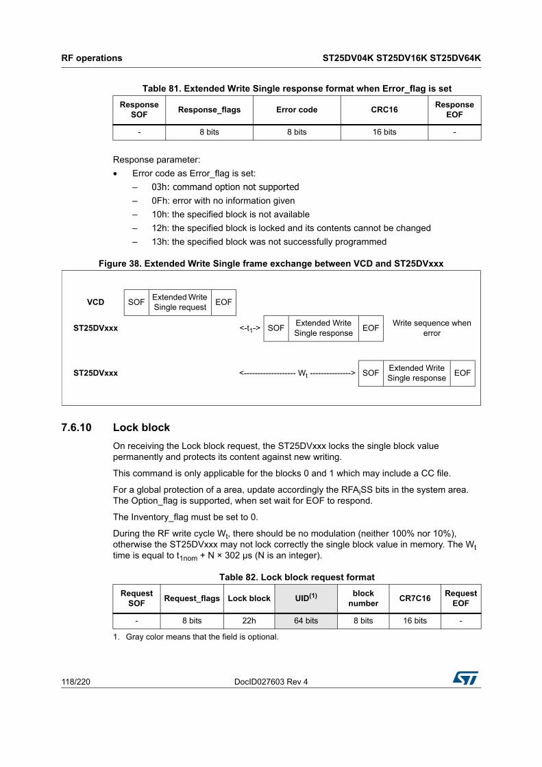
RF operations ST25DV04K ST25DV16K ST25DV64K
118/220 DocID027603 Rev 4
Response parameter:
• Error code as Error_flag is set:
– 03h: command option not supported– 0Fh: error with no information given
– 10h: the specified block is not available
– 12h: the specified block is locked and its contents cannot be changed
– 13h: the specified block was not successfully programmed
7.6.10 Lock block
On receiving the Lock block request, the ST25DVxxx locks the single block value permanently and protects its content against new writing.
This command is only applicable for the blocks 0 and 1 which may include a CC file.
For a global protection of a area, update accordingly the RFAiSS bits in the system area. The Option_flag is supported, when set wait for EOF to respond.
The Inventory_flag must be set to 0.
During the RF write cycle Wt, there should be no modulation (neither 100% nor 10%), otherwise the ST25DVxxx may not lock correctly the single block value in memory. The Wt time is equal to t1nom + N × 302 µs (N is an integer).
Table 81. Extended Write Single response format when Error_flag is set
Response SOF
Response_flags Error code CRC16Response
EOF
- 8 bits 8 bits 16 bits -
Figure 38. Extended Write Single frame exchange between VCD and ST25DVxxx
VCD SOFExtended Write Single request
EOF
ST25DVxxx <-t1-> SOFExtended Write Single response
EOFWrite sequence when
error
ST25DVxxx <------------------- Wt ---------------> SOFExtended Write Single response
EOF
Table 82. Lock block request format
Request SOF
Request_flags Lock block UID(1)
1. Gray color means that the field is optional.
block number
CR7C16Request
EOF
- 8 bits 22h 64 bits 8 bits 16 bits -

DocID027603 Rev 4 119/220
ST25DV04K ST25DV16K ST25DV64K RF operations
219
Request parameter:
• Request Flags
• UID (optional)
• Block number (only value 00h or 01h) are allowed to protect the CCfile in case of NDEF usage.
Response parameter:
• No parameter
Response parameter:
• Error code as Error_flag is set
– 03h: command option not supported
– 10h: block not available
– 11h: the specified block is already locked and thus cannot be locked again
– 14h: the specified block was not successfully locked
Table 83. Lock block response format when Error_flag is NOT set
Response SOF
Response_flags CRC16Response
EOF
- 8 bits 16 bits -
Table 84. Lock single block response format when Error_flag is set
Response SOF
Response_flags Error code CRC16Response
EOF
- 8 bits 8 bits 16 bits -
Figure 39. Lock single block frame exchange between VCD and ST25DVxxx
VCD SOFLock block
requestEOF
ST25DVxxx <-t1-> SOFLock block response
EOFLock sequence
when error
ST25DVxxx <----------------- Wt -----------> SOFLock block response
EOF

RF operations ST25DV04K ST25DV16K ST25DV64K
120/220 DocID027603 Rev 4
7.6.11 Extended Lock block
On receiving the extended Lock block request, the ST25DVxxx locks the single block value permanently and protects its content against new writing.
This command is only applicable for the blocks 0 and 1 which may include a CC file.
For a global protection of a area, update accordingly the AiSS bits in the system area. When the Option_flag is set, wait for EOF to respond.
The Inventory_flag must be set to 0.
During the RF write cycle Wt, there should be no modulation (neither 100% nor 10%), otherwise the ST25DVxxx may not lock correctly the single block value in memory. The Wt time is equal to t1nom + N × 302 µs (N is an integer).
Request parameter:
• Request Flags
• UID (optional)
• Block number (only value 00h or 01h) are allowed to protect the CCfile in case of NDEF usage.
Response parameter:
• No parameter
Response parameter:
• Error code as Error_flag is set
– 03h: command option not supported
– 10h: block not available
– 11h: the specified block is already locked and thus cannot be locked again
– 14h: the specified block was not successfully locked
Table 85. Extended Lock block request format
Request SOF
Request_flagsExtended
Lock blockUID(1)
1. Gray color means that the field is optional.
block number
CRC16Request
EOF
- 8 bits 32h 64 bits 16 bits 16 bits -
Table 86. Extended Lock block response format when Error_flag is NOT set
Response SOF
Response_flags CRC16Response
EOF
- 8 bits 16 bits -
Table 87. Extended Lock block response format when Error_flag is set
Response SOF
Response_flags Error code CRC16Response
EOF
- 8 bits 8 bits 16 bits -

DocID027603 Rev 4 121/220
ST25DV04K ST25DV16K ST25DV64K RF operations
219
7.6.12 Read Multiple Blocks
When receiving the Read Multiple Block command, the ST25DVxxx reads the selected blocks and sends back their value in multiples of 32 bits in the response. The blocks are numbered from 00h to FFh in the request and the value is minus one (–1) in the field. For example, if the “Number of blocks” field contains the value 06h, seven blocks are read. The maximum number of blocks is fixed at 256 assuming that they are all located in the same area. If the number of blocks overlaps areas or overlaps the end of user memory, the ST25DVxxx returns an error code. When the Option_flag is set, the response returns the Block Security Status.
The Inventory_flag must be set to 0.
Block number is coded on 1 Byte and only first 256 blocks of ST25DV16K-xx and ST25DV64K-xx can be addressed using this command.
Request parameters:
• Request flags
• UID (optional)
• First block number
• Number of blocks
Figure 40. Extended Lock block frame exchange between VCDand ST25DVxxx
VCD SOF
Extended Lock block
request
EOF
ST25DVxxx <-t1-> SOFExtended Lock block response
EOFLock sequence
when error
ST25DVxxx <----------------- Wt -----------> SOFExtended Lock block response
EOF
Table 88. Read Multiple Block request format
Request SOF
Request_flags
Read Multiple Block
UID(1)
1. Gray color means that the field is optional.
First block number
Number of blocks
CRC16Request
EOF
- 8 bits 23h 64 bits 8 bits 8 bits 16 bits -

RF operations ST25DV04K ST25DV16K ST25DV64K
122/220 DocID027603 Rev 4
Response parameters:
• Block security status if Option_flag is set (see Table 90: Block security status)
• N blocks of data
Response parameter:
• Error code as Error_flag is set:
– 03h: command option is not supported
– 0Fh: error with no information given
– 10h: the specified block is not available
– 15h: the specified block is read-protected
7.6.13 Extended Read Multiple Blocks
When receiving the Extended Read multiple block command, the ST25DVxxx reads the selected blocks and sends back their value in multiples of 32 bits in the response. The blocks are numbered from 00h to last block of memory in the request and the value is minus one (-1) in the field. For example, if the “Number of blocks” field contains the value 06h, seven blocks are read. The maximum number of blocks is fixed at 2047 assuming that they are all located in the same area. If the number of blocks overlaps areas or overlaps the end
Table 89. Read Multiple Block response format when Error_flag is NOT set
Response SOF
Response_flags
Block security status(1)
1. Gray color means that the field is optional.
Data CRC16Response
EOF
- 8 bits 8 bits(2)
2. Repeated as needed.
32 bits(2) 16 bits -
Table 90. Block security status
b7 b6 b5 b4 b3 b2 b1 b0
Reserved for future use.All at 0.
0: Current block not locked 1: Current block locked
Table 91. Read Multiple Block response format when Error_flag is set
Response SOF Response_flags Error code CRC16 Response EOF
- 8 bits 8 bits 16 bits -
Figure 41. Read Multiple Block frame exchange between VCD and ST25DVxxx
VCD SOFRead Multiple Block request
EOF
ST25DVxxx <-t1-> SOFRead Multiple
Block responseEOF

DocID027603 Rev 4 123/220
ST25DV04K ST25DV16K ST25DV64K RF operations
219
of user memory, the ST25DVxxx returns an error code. When the Option_flag is set, the response returns the Block Security Status.
The Inventory_flag must be set to 0.
Block number is coded on 2 Bytes so all memory blocks of ST25DV16K-xx and ST25DV64K-xx can be addressed using this command.
Request parameters:
• Request flags
• UID (optional)
• First block number
• Number of blocks
Response parameters:
• Block security status if Option_flag is set (see Table 94: Block security status)
• N blocks of data
Table 92. Extended Read Multiple Block request format
Request SOF
Request_flags
Extended Read Multiple
BlockUID(1)
1. Gray color means that the field is optional.
First block number
Number of blocks
CRC16Request
EOF
- 8 bits 33h 64 bits 16 bits 16 bits 16 bits -
Table 93. Extended Read Multiple Block response format when Error_flag is NOT set
Response SOF
Response_flags
Block security status(1)
1. Gray color means that the field is optional.
Data CRC16Response
EOF
- 8 bits 8 bits(2)
2. Repeated as needed.
32 bits(2) 16 bits -
Table 94. Block security status
b7 b6 b5 b4 b3 b2 b1 b0
Reserved for future use.All at 0
0: Current block not locked 1: Current block locked
Table 95. Extended Read Multiple Block response format when Error_flag is set
Response SOF Response_flags Error code CRC16 Response EOF
- 8 bits 8 bits 16 bits -

RF operations ST25DV04K ST25DV16K ST25DV64K
124/220 DocID027603 Rev 4
Response parameter:
• Error code as Error_flag is set:
– 03h: command option is not supported
– 0Fh: error with no information given
– 10h: the specified block is not available
– 15h: the specified block is read-protected
7.6.14 Write Multiple Blocks
On receiving the Write Multiple Block command, the ST25DVxxx writes the data contained in the request to the requested blocks, and reports whether the write operation were successful in the response. ST25DVxxx supports up to 4 blocks, data field must be coherent with the number of blocks to program.
If some blocks overlaps areas, or overlap end of user memory, the ST25DVxxx returns an error code and none of the blocks are programmed. When the Option_flag is set, wait for EOF to respond. During the RF write cycle Wt, there should be no modulation (neither 100% nor 10%), otherwise the ST25DVxxx may not program correctly the data into the memory. The Wt time is equal to t1nom + m × 302 μs < 20 ms. (m is an integer, it is function of Nb number of blocks to be programmed).
The Inventory_flag must be set to 0.
Block number is coded on 1 Byte and only first 256 blocks of ST25DV16K-xx and ST25DV64K-xx can be addressed using this command.
Figure 42. Extended Read Multiple Block frame exchange between VCD and ST25DVxxx
VCD SOFExtended
Read Multiple Block request
EOF
ST25DVxxx <-t1-> SOFExtended Read Multiple Block
responseEOF
Table 96. Write Multiple Block request format
Request SOF
Request_flagsWrite
Multiple Block
UID(1)First Block
number
Number of
block(2)Data CRC16
Request EOF
- 8 bits 24h 64 bits 8 bits 8 bitsBlock
length(3) 16 bits -
1. Gray color means that the field is optional.
2. The number of blocks in the request is one less than the number of blocks that the VICC shall write.
3. Repeated as needed

DocID027603 Rev 4 125/220
ST25DV04K ST25DV16K ST25DV64K RF operations
219
Request parameters:
• Request flags
• UID (optional)
• First Block number
• Number of blocks
• Data
Response parameter:
• No parameter. The response is sent back after the writing cycle.
Response parameter:
• Error code as Error_flag is set:
– 03h: command option is not supported
– 0Fh: error with no information given
– 10h: the specified block is not available
– 12h: the specified block is locked and its contents cannot be changed
– 13h: the specified block was not successfully programmed
Table 97. Write Multiple Block response format when Error_flag is NOT set
Response SOF Response_flags CRC16 Response EOF
- 8 bits 16 bits -
Table 98. Write Multiple Block response format when Error_flag is set
Response SOF
Response_flags Error code CRC16Response
EOF
- 8 bits 8 bits 16 bits -
Figure 43. Write Multiple Block frame exchange between VCD and ST25DVxxx
VCD SOFWrite Multiple Block request
EOF
ST25DVxxx <-t1-> SOFWrite Multiple
Block responseEOF
Write sequence when error
ST25DVxxx <---------------- m * Wt ------------> SOFWrite Multiple
Block responseEOF

RF operations ST25DV04K ST25DV16K ST25DV64K
126/220 DocID027603 Rev 4
7.6.15 Extended Write Multiple Blocks
On receiving the Extended Write multiple block command, the ST25DVxxx writes the data contained in the request to the targeted blocks and reports whether the write operation were successful in the response. ST25DVxxx supports up to 4 blocks, data field must be coherent with number of blocks to program.
If some blocks overlaps areas, or overlap end of user memory the ST25DVxxx returns an error code and none of the blocks are programmed.
When the Option_flag is set, wait for EOF to respond. During the RF write cycle Wt, there should be no modulation (neither 100% nor 10%), otherwise the ST25DVxxx may not program correctly the data into the memory. The Wt time is equal to t1nom + m × 302 μs < 20 ms (m is an integer function of Nb number of blocks to be programmed).
The inventory_flag must be set to 0.
Block number is coded on 2 Bytes so all memory blocks of ST25DV16K-xx and ST25DV64K-xx can be addressed using this command.
Request parameters:
• Request flags
• UID (optional)
• First block number
• Number of block
• Data (from first to last blocks, from LSB bytes to MSB bytes)
Response parameter:
• No parameter. The response is sent back after the writing cycle.
Table 99. Extended Write Multiple Block request format
Request SOF
Request_flags
Extended Write
multiple block
UID(1)First Block
number
Number of
block(2)Data CRC16
Request EOF
- 8 bits 34h 64 bits 16 bits 16 bitsBlock
length(3) 16 bits -
1. Gray color means that the field is optional.
2. The number of blocks in the request is one less than the number of blocks that the VICC shall write.
3. Repeated as needed
Table 100. Extended Write Multiple Block response format when Error_flag is NOT set
Response SOF Response_flags CRC16 Response EOF
- 8 bits 16 bits -

DocID027603 Rev 4 127/220
ST25DV04K ST25DV16K ST25DV64K RF operations
219
Response parameter:
• Error code as Error_flag is set:
– 03h: command option is not supported
– 0Fh: error with no information given
– 10h: the specified block is not available
– 12h: the specified block is locked and its contents cannot be changed
– 13h: the specified block was not successfully programmed
7.6.16 Select
When receiving the Select command:
• If the UID is equal to its own UID, the ST25DVxxx enters or stays in the Selected state and sends a response.
• If the UID does not match its own UID, the selected ST25DVxxx returns to the Ready state and does not send a response.
The ST25DVxxx answers an error code only if the UID is equal to its own UID. If not, no response is generated. If an error occurs, the ST25DVxxx remains in its current state.
The Option_flag is not supported, and the Inventory_flag must be set to 0.
Table 101. Extended Write Multiple Block response format when Error_flag is set
Response SOF
Response_flags Error code CRC16Response
EOF
- 8 bits 8 bits 16 bits -
Figure 44. Extended Write Multiple Block frame exchange between VCD and ST25DVxxx
VCD SOFExtended Write Multiple Block
requestEOF
ST25DVxxx <-t1-> SOFExtended Write Multiple Block
responseEOF
Write sequence when error
ST25DVxxx <------------------- Wt ---------------> SOFExtended Write Multiple Block
responseEOF
Table 102. Select request format
Request SOF
Request_flags Select UID CRC16Request
EOF
- 8 bits 25h 64 bits 16 bits -
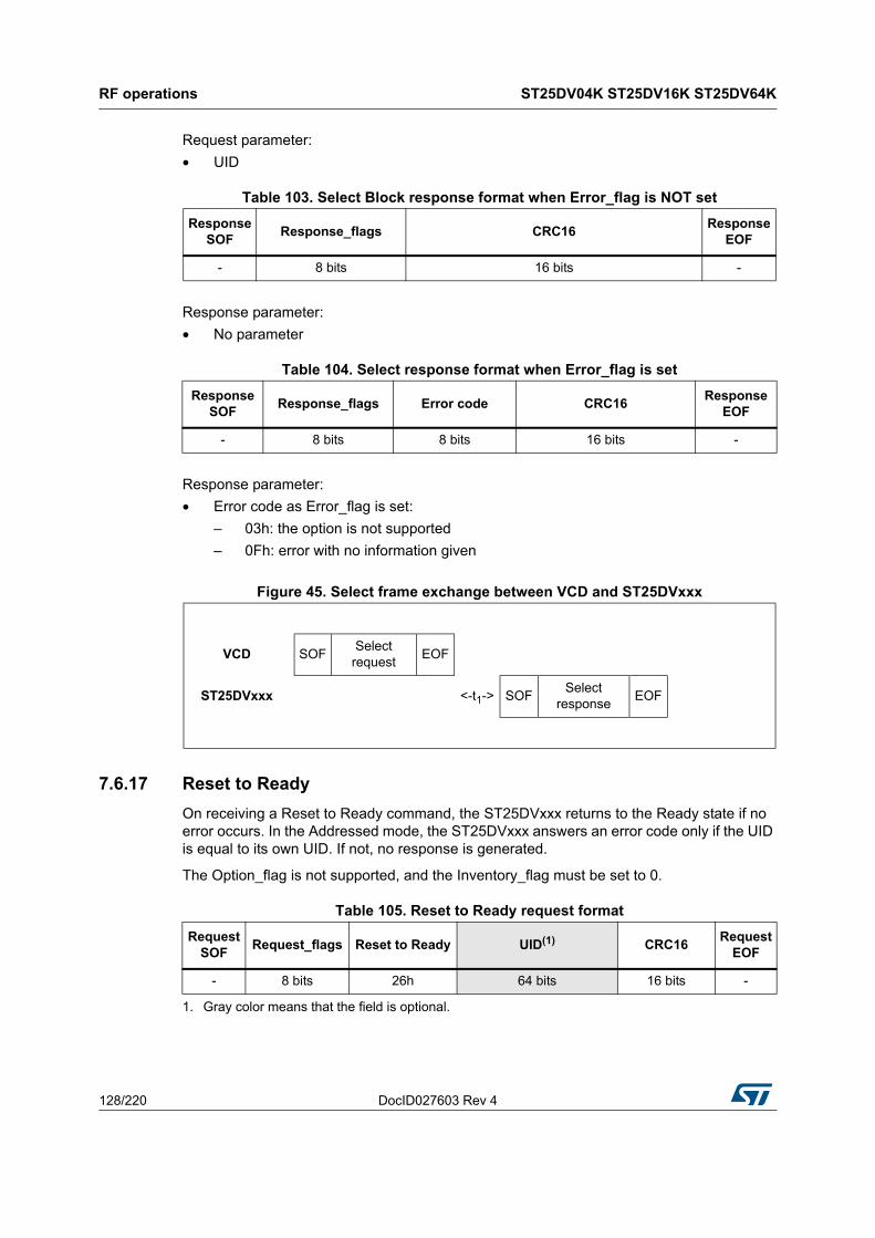
RF operations ST25DV04K ST25DV16K ST25DV64K
128/220 DocID027603 Rev 4
Request parameter:
• UID
Response parameter:
• No parameter
Response parameter:
• Error code as Error_flag is set:
– 03h: the option is not supported
– 0Fh: error with no information given
7.6.17 Reset to Ready
On receiving a Reset to Ready command, the ST25DVxxx returns to the Ready state if no error occurs. In the Addressed mode, the ST25DVxxx answers an error code only if the UID is equal to its own UID. If not, no response is generated.
The Option_flag is not supported, and the Inventory_flag must be set to 0.
Table 103. Select Block response format when Error_flag is NOT set
Response SOF
Response_flags CRC16Response
EOF
- 8 bits 16 bits -
Table 104. Select response format when Error_flag is set
Response SOF
Response_flags Error code CRC16Response
EOF
- 8 bits 8 bits 16 bits -
Figure 45. Select frame exchange between VCD and ST25DVxxx
VCD SOFSelect
requestEOF
ST25DVxxx <-t1-> SOFSelect
responseEOF
Table 105. Reset to Ready request format
Request SOF
Request_flags Reset to Ready UID(1)
1. Gray color means that the field is optional.
CRC16Request
EOF
- 8 bits 26h 64 bits 16 bits -

DocID027603 Rev 4 129/220
ST25DV04K ST25DV16K ST25DV64K RF operations
219
Request parameter:
• UID (optional)
Response parameter:
• No parameter
Response parameter:
• Error code as Error_flag is set:
– 03h: the option is not supported
– 0Fh: error with no information given
7.6.18 Write AFI
On receiving the Write AFI request, the ST25DVxxx programs the 8-bit AFI value to its memory. When the Option_flag is set, wait for EOF to respond.
The Inventory_flag must be set to 0.
During the RF write cycle Wt, there should be no modulation (neither 100% nor 10%), otherwise the ST25DVxxx may not write correctly the AFI value into the memory. The Wt time is equal to t1nom + N × 302 µs (N is an integer).
Table 106. Reset to Ready response format when Error_flag is NOT set
Response SOF
Response_flags CRC16Response
EOF
- 8 bits 16 bits -
Table 107. Reset to ready response format when Error_flag is set
Response SOF
Response_flags Error code CRC16Response
EOF
- 8 bits 8 bits 16 bits -
Figure 46. Reset to Ready frame exchange between VCD and ST25DVxxx
VCD SOFReset to Ready request
EOF
ST25DVxxx <-t1-> SOFReset to Ready
responseEOF

RF operations ST25DV04K ST25DV16K ST25DV64K
130/220 DocID027603 Rev 4
Request parameter:
• Request flags
• UID (optional)
• AFI
Response parameter:
• No parameter
Response parameter:
• Error code as Error_flag is set
– 03h: command option is not supported
– 0Fh: error with no information given
– 12h: the specified block is locked and its contents cannot be changed
– 13h: the specified block was not successfully programmed
Table 108. Write AFI request format
Request SOF
Request_flags Write AFI UID(1)
1. Gray color means that the field is optional.
AFI CRC16Request
EOF
- 8 bits 27h 64 bits 8 bits 16 bits -
Table 109. Write AFI response format when Error_flag is NOT set
Response SOF
Response_flags CRC16Response
EOF
- 8 bits 16 bits -
Table 110. Write AFI response format when Error_flag is set
Response SOF
Response_flags
Error code CRC16Response
EOF
- 8 bits 8 bits 16 bits -
Figure 47. Write AFI frame exchange between VCD and ST25DVxxx
VCD SOFWrite AFI request
EOF
ST25DVxxx <-t1-> SOFWrite AFI response
EOFWrite sequence
when error
ST25DVxxx <------------------ Wt --------------> SOFWrite AFI response
EOF
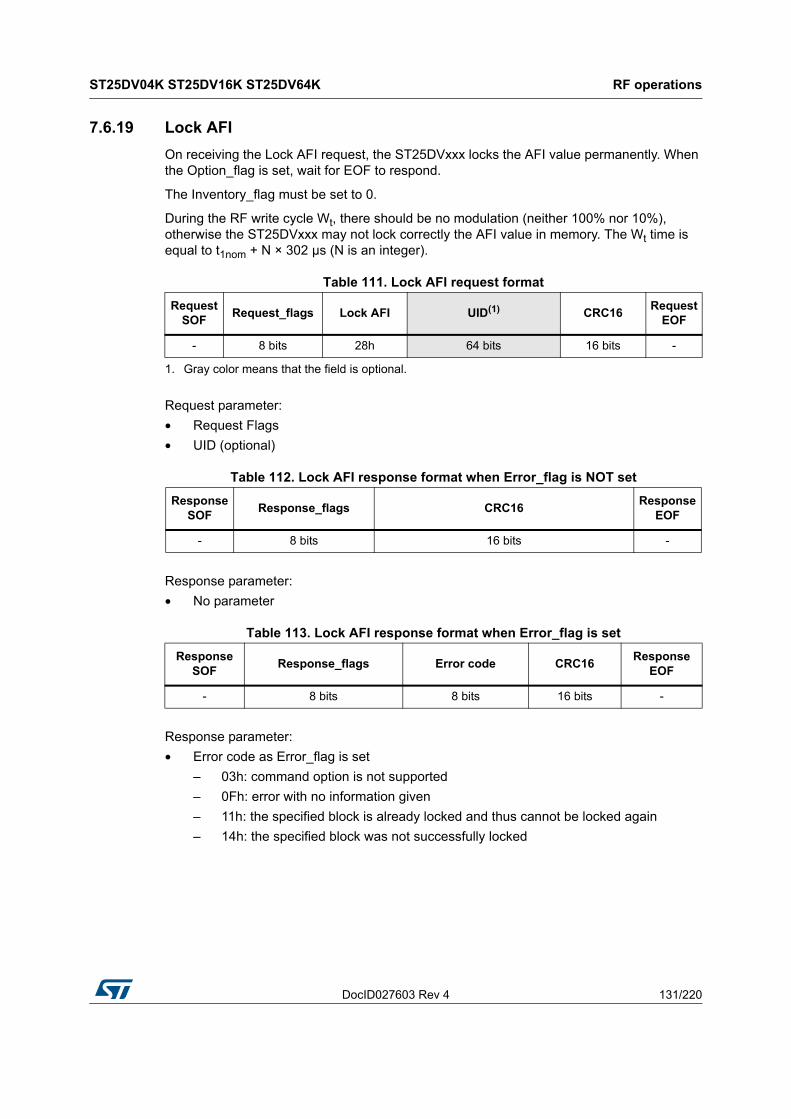
DocID027603 Rev 4 131/220
ST25DV04K ST25DV16K ST25DV64K RF operations
219
7.6.19 Lock AFI
On receiving the Lock AFI request, the ST25DVxxx locks the AFI value permanently. When the Option_flag is set, wait for EOF to respond.
The Inventory_flag must be set to 0.
During the RF write cycle Wt, there should be no modulation (neither 100% nor 10%), otherwise the ST25DVxxx may not lock correctly the AFI value in memory. The Wt time is equal to t1nom + N × 302 µs (N is an integer).
Request parameter:
• Request Flags
• UID (optional)
Response parameter:
• No parameter
Response parameter:
• Error code as Error_flag is set
– 03h: command option is not supported
– 0Fh: error with no information given
– 11h: the specified block is already locked and thus cannot be locked again
– 14h: the specified block was not successfully locked
Table 111. Lock AFI request format
Request SOF
Request_flags Lock AFI UID(1)
1. Gray color means that the field is optional.
CRC16Request
EOF
- 8 bits 28h 64 bits 16 bits -
Table 112. Lock AFI response format when Error_flag is NOT set
Response SOF
Response_flags CRC16Response
EOF
- 8 bits 16 bits -
Table 113. Lock AFI response format when Error_flag is set
Response SOF
Response_flags Error code CRC16Response
EOF
- 8 bits 8 bits 16 bits -

RF operations ST25DV04K ST25DV16K ST25DV64K
132/220 DocID027603 Rev 4
7.6.20 Write DSFID
On receiving the Write DSFID request, the ST25DVxxx programs the 8-bit DSFID value to its memory. When the Option_flag is set, wait for EOF to respond.
The Inventory_flag must be set to 0.
During the RF write cycle Wt, there should be no modulation (neither 100% nor 10%), otherwise the ST25DVxxx may not write correctly the DSFID value in memory. The Wt time is equal to t1nom + N × 302 µs (N is an integer).
Request parameter:
• Request flags
• UID (optional)
• DSFID
Response parameter:
• No parameter
Figure 48. Lock AFI frame exchange between VCD and ST25DVxxx
VCD SOFLock AFI request
EOF
ST25DVxxx <-t1-> SOFLock AFI response
EOFLock sequence
when error
ST25DVxxx <----------------- Wt -----------> SOFLock AFI response
EOF
Table 114. Write DSFID request format
Request SOF
Request_flags Write DSFID UID(1)
1. Gray color means that the field is optional.
DSFID CRC16Request
EOF
- 8 bits 29h 64 bits 8 bits 16 bits -
Table 115. Write DSFID response format when Error_flag is NOT set
Response SOF
Response_flags CRC16Response
EOF
- 8 bits 16 bits -

DocID027603 Rev 4 133/220
ST25DV04K ST25DV16K ST25DV64K RF operations
219
Response parameter:
• Error code as Error_flag is set
– 03h: command option is not supported
– 0Fh: error with no information given
– 12h: the specified block is locked and its contents cannot be changed
– 13h: the specified block was not successfully programmed
7.6.21 Lock DSFID
On receiving the Lock DSFID request, the ST25DVxxx locks the DSFID value permanently. When the Option_flag is set, wait for EOF to respond.
The Inventory_flag must be set to 0.
During the RF write cycle Wt, there should be no modulation (neither 100% nor 10%), otherwise the ST25DVxxx may not lock correctly the DSFID value in memory. The Wt time is equal to t1nom + N × 302 µs (N is an integer).
Request parameter:
• Request flags
• UID (optional)
Table 116. Write DSFID response format when Error_flag is set
Response SOF
Response_flags Error code CRC16Response
EOF
- 8 bits 8 bits 16 bits -
Figure 49. Write DSFID frame exchange between VCD and ST25DVxxx
VCD SOFWrite DSFID
requestEOF
ST25DVxxx <-t1->SOF
Write DSFID response
EOF
Write sequence when error
ST25DVxxx <---------------- Wt ---------->SOF
Write DSFID response
EOF
Table 117. Lock DSFID request format
Request SOF
Request_flags Lock DSFID UID(1)
1. Gray color means that the field is optional.
CRC16Request
EOF
- 8 bits 2Ah 64 bits 16 bits -

RF operations ST25DV04K ST25DV16K ST25DV64K
134/220 DocID027603 Rev 4
Response parameter:
• No parameter.
Response parameter:
• Error code as Error_flag is set:
– 03h: command option is not supported
– 0Fh: error with no information given
– 11h: the specified block is already locked and thus cannot be locked again
– 14h: the specified block was not successfully locked
7.6.22 Get System Info
When receiving the Get System Info command, the ST25DVxxx sends back its information data in the response.
The Option_flag is not supported. The Inventory_flag must be set to 0. The Get System Info can be issued in both Addressed and Non Addressed modes.
Table 118. Lock DSFID response format when Error_flag is NOT set
Response SOF
Response_flags CRC16Response
EOF
- 8 bits 16 bits -
Table 119. Lock DSFID response format when Error_flag is set
Response SOF
Response_flags Error code CRC16Response
EOF
- 8 bits 8 bits 16 bits -
Figure 50. Lock DSFID frame exchange between VCD and ST25DVxxx
VCD SOFLock
DSFID request
EOF
ST25DVxxx <-t1-> SOFLock DSFID
responseEOF
Lock sequence when error
ST25DVxxx <---------------- Wt -------------> SOFLock
DSFID response
EOF
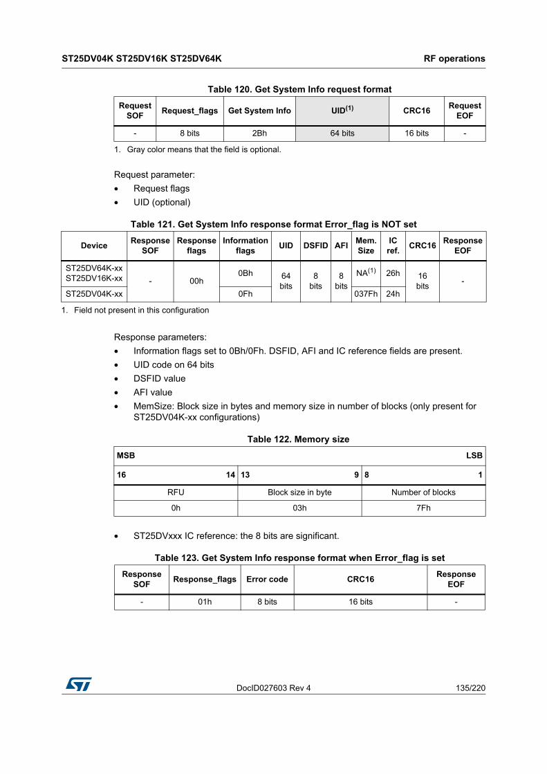
DocID027603 Rev 4 135/220
ST25DV04K ST25DV16K ST25DV64K RF operations
219
Request parameter:
• Request flags
• UID (optional)
Response parameters:
• Information flags set to 0Bh/0Fh. DSFID, AFI and IC reference fields are present.
• UID code on 64 bits
• DSFID value
• AFI value
• MemSize: Block size in bytes and memory size in number of blocks (only present for ST25DV04K-xx configurations)
• ST25DVxxx IC reference: the 8 bits are significant.
Table 120. Get System Info request format
Request SOF
Request_flags Get System Info UID(1)
1. Gray color means that the field is optional.
CRC16Request
EOF
- 8 bits 2Bh 64 bits 16 bits -
Table 121. Get System Info response format Error_flag is NOT set
DeviceResponse
SOFResponse
flagsInformation
flagsUID DSFID AFI
Mem.Size
IC ref.
CRC16Response
EOF
ST25DV64K-xxST25DV16K-xx - 00h
0Bh 64 bits
8 bits
8bits
NA(1) 26h 16 bits
-
ST25DV04K-xx 0Fh 037Fh 24h
1. Field not present in this configuration
Table 122. Memory size
MSB LSB
16 14 13 9 8 1
RFU Block size in byte Number of blocks
0h 03h 7Fh
Table 123. Get System Info response format when Error_flag is set
Response SOF
Response_flags Error code CRC16Response
EOF
- 01h 8 bits 16 bits -

RF operations ST25DV04K ST25DV16K ST25DV64K
136/220 DocID027603 Rev 4
Response parameter:
• Error code as Error_flag is set:
– 03h: Option not supported
– 0Fh: error with no information given
.
7.6.23 Extended Get System Info
When receiving the Extended Get System Info command, the ST25DVxxx sends back its information data in the response.
The Option_flag is not supported. The Inventory_flag must be set to 0. The Extended Get System Info can be issued in both Addressed and Non Addressed modes.
• Request flags
• Request parameters
• UID (optional)
M
Figure 51. Get System Info frame exchange between VCD and ST25DVxxx
VCD SOFGet System Info
requestEOF
ST25DVxxx <-t1-> SOFGet System Info
responseEOF
Table 124. Extended Get System Info request format
Request SOF
Request_flagsExtended
Get System Info
Parameter request field
UID(1)
1. Gray color means that the field is optional.
CRC16Request
EOF
- 8 bits 3Bh 8 bits 64 bits 16 bits -
Table 125. Parameter request list
Bit Flag name Value Description
b1 DSFID0 No request of DSFID
1 Request of DSFID
b2 AFI0 No request of AFI
1 Request of AFI
b3 VICC memory size0 No request of data field on VICC memory size
1 Request of data field on VICC memory size
b4 IC reference0 No request of Information on IC reference
1 Request of Information on IC reference
b5 MOI 1 Information on MOI always returned in response flag

DocID027603 Rev 4 137/220
ST25DV04K ST25DV16K ST25DV64K RF operations
219
Response parameters:
• Information flag defining which fields are present
• UID code on 64 bits
• DSFID value (if requested in Parameters request field)
• AFI value (if requested in Parameters request field)
• Other fields:
– VICC Memory size (if requested in Parameters request field)
– ICRef (if requested in Parameters request field)
– VICC Command list (if requested in Parameters request field)
b6 VICC Command list0 No request of Data field of all supported commands
1 Request of Data field of all supported commands
b7 CSI Information0 No request of CSI list
1 Request of CSI list
b8Extended Get System
Info parameter Field0
One byte length of Extended Get System
Info parameter field
Table 125. Parameter request list (continued)
Bit Flag name Value Description
Table 126. Extended Get System Info response format when Error_flag is NOT set
Response SOF
Response_flags
Information flags
UID DSFID(1)(2) AFI(1)(2) Other Field(1)(2) CRC16
Response EOF
- 00h 8 bits(2) 64 bits
8 bits 8 bits up to 64 bits(3) 16 bits -
1. Gray color means that the field is optional.
2. See Table 127: Response Information Flag.
3. Number of bytes is function of parameter list selected.
Table 127. Response Information Flag
Bit Flag name Value Description
b1 DSFID0 DSFID field is not present
1 DSFID field is present
b2 AFI0 AFI field is not present
1 AFI field is present
b3 VICC memory size0 Data field on VICC memory size is not present.
1 Data field on VICC memory size is present.
b4 IC reference0 Information on IC reference field is not present.
1 Information on IC reference field is present.

RF operations ST25DV04K ST25DV16K ST25DV64K
138/220 DocID027603 Rev 4
b5 MOI0 1 byte addressing
1 2 byte addressing
b6 VICC Command list0 Data field of all supported commands is not present
1 Data field of all supported commands is present
b7 CSI Information 0 CSI list is not present
b8 Info flag Field 0 One byte length of Info flag field
Table 128. Response other field: ST25DVxxx VICC memory size
MSB LSB
24 22 21 17 16 01
RFU Block size in byte Number of blocks
0h 03h07FFh (ST25DV64K-xx)01FFh (ST25DV16K-xx)007Fh (ST25DV04K-xx)
Table 129. Response other field: ST25DVxxx IC Ref
1 byte
ICRef
24h (ST25DV04K-XX) or 26h (ST25DV16K-xx and ST25DV64K-xx)
Table 130. Response other field: ST25DVxxx VICC command list
MSB LSB
32 25 24 17 16 09 08 01
Byte 4 Byte3 Byte 2 Byte 1
00h 3Fh 3Fh FFh
Table 131. Response other field: ST25DVxxx VICC command list Byte 1
Bit Meaning if bit is set Comment
b1 Read single block is supported -
b2 Write single block is supported -
b3 Lock single block is supported -
Table 127. Response Information Flag (continued)
Bit Flag name Value Description
DocID027603 Rev 4 139/220
ST25DV04K ST25DV16K ST25DV64K RF operations
219
b4 Read multiple block is supported -
b5 Write multiple block is supported -
b6 Select is supported including Select state
b7 Reset to Ready is supported -
b8 Get multiple block security status is supported -
Table 132. Response other field: ST25DVxxx VICC command list Byte 2
Bit Meaning if bit is set Comment
b1 Write AFI is supported -
b2 Lock AFI is supported -
b3 Write DSFID is supported -
b4 Lock DSFID is supported -
b5 Get System Information is supported -
b6 Custom commands are supported -
b7 RFU 0 shall be returned
b8 RFU 0 shall be returned
Table 133. Response other field: ST25DVxxx VICC command list Byte 3
Bit Meaning if bit is set Comment
b1 Extended read single block is supported -
b2 Extended write single block is supported -
b3 Extended lock single block is supported -
b4 Extended read multiple block is supported -
b5 Extended write multiple block is supported -
b6 Extended Get Multiple Security Status is supported -
b7 RFU 0 shall be returned
b8 RFU 0 shall be returned
Table 131. Response other field: ST25DVxxx VICC command list Byte 1 (continued)
Bit Meaning if bit is set Comment

RF operations ST25DV04K ST25DV16K ST25DV64K
140/220 DocID027603 Rev 4
Response parameter:
• Error code as Error_flag is set:
– 03h: Option not supported
– 0Fh: error with no information given
.
7.6.24 Get Multiple Block Security Status
When receiving the Get Multiple Block Security Status command, the ST25DVxxx sends back its security status for each address block: 0 when block is writable else 1 when block is locked for writing. The blocks security status are defined by the area security status (and by LCK_CCFILE register for blocks 0 and 1). The blocks are numbered from 00h up to the maximum memory block number in the request, and the value is minus one (–1) in the field. For example, a value of “06” in the “Number of blocks” field requests will return the security status of seven blocks. This command does not respond an error if number of blocks overlap areas or overlap the end of the user memory.
Table 134. Response other field: ST25DVxxx VICC command list Byte 4
Bit Meaning if bit is set Comment
b1 Read Buffer is supported Means Response Buffer is supported
b2 Select Secure State is supportedMeans VCD or Mutual authentication
are supported
b3 Final Response always includes crypto resultMeans that flag b3 will be set in the
Final response
b4 AuthComm crypto format is supported -
b5 SecureComm crypto format is supported -
b6 KeyUpdate is supported -
b7 Challenge is supported -
b8 If set to 1 a further Byte is transmitted 0 shall be returned
Table 135. Extended Get System Info response format when Error_flag is set
Response SOF
Response_flags Error code CRC16Response
EOF
- 01h 8 bits 16 bits -
Figure 52. Extended Get System Info frame exchange between VCD and ST25DVxxx
VCD SOFExtended Get System Info
requestEOF
ST25DVxxx <-t1-> SOFExtended Get System
Info responseEOF

DocID027603 Rev 4 141/220
ST25DV04K ST25DV16K ST25DV64K RF operations
219
The number of blocks is coded on 1 Byte and only first 256 blocks of ST25DV16K-xx and ST25DV64K-xx can be addressed using this command.
The Option_flag is not supported. The Inventory_flag must be set to 0.
Request parameter:
• Request flags
• UID (optional)
• First block number
• Number of blocks
Response parameters:
• Block security status
Response parameter:
• Error code as Error_flag is set:
– 03h: the option is not supported
– 0Fh: error with no information given
– 10h: the specified block is not available
Table 136. Get Multiple Block Security Status request format
Request SOF
Request_flags
Get Multiple Block Security Status
UID(1)
1. Gray color means that the field is optional.
First block number
Number of blocks
CRC16Request
EOF
- 8 bits 2Ch 64 bits 8 bits 8 bits 16 bits -
Table 137. Get Multiple Block Security Status response format when Error_flag is NOT set
Response SOF
Response_flags Block security status CRC16Response
EOF
- 8 bits 8 bits(1)
1. Repeated as needed.
16 bits -
Table 138. Block security status
b7 b6 b5 b4 b3 b2 b1 b0
Reserved for future useAll at 0
0: Current block not locked
1: Current block locked
Table 139. Get Multiple Block Security Status response format when Error_flag is set
Response SOF
Response_flags Error code CRC16Response
EOF
- 8 bits 8 bits 16 bits -

RF operations ST25DV04K ST25DV16K ST25DV64K
142/220 DocID027603 Rev 4
7.6.25 Extended Get Multiple Block Security Status
When receiving the Extended Get Multiple Block Security Status command, the ST25DVxxx sends back the security status for each address block: 0 when the block is writable else 1 when block is locked for writing. The block security statuses are defined by the area security status. The blocks are numbered from 00h up to the maximum memory block number in the request, and the value is minus one (–1) in the field. For example, a value of '06' in the “Number of blocks” field requests to return the security status of seven blocks.
This command does not respond an error if number of blocks overlap areas or overlap the end of the user memory.
The number of blocks is coded on 2 Bytes so all memory blocks of ST25DV16K-xx and ST25DV64K-xx can be addressed using this command.
The Option_flag is not supported. The Inventory_flag must be set to 0.
Request parameter:
• Request flags
• UID (optional)
• First block number
• Number of blocks
Figure 53. Get Multiple Block Security Status frame exchange between VCD and ST25DVxxx
VCD SOF Get Multiple Block Security Request
statusEOF
ST25DVxxx <-t1-> SOFGet Multiple Block
Security Response status
EOF
Table 140. Extended Get Multiple Block Security Status request format
Request SOF
Request_flags
Extended Get Multiple Block Security Status
UID(1)
1. Gray color means that the field is optional.
First block number
Number of blocks
CRC16Request
EOF
- 8 bits 3Ch 64 bits 16 bits 16 bits 16 bits -
Table 141. Extended Get Multiple Block Security Status response format when Error_flags NOT set
Response SOF
Response_flags Block security status CRC16Response
EOF
- 8 bits 8 bits(1)
1. Repeated as needed.
16 bits -

DocID027603 Rev 4 143/220
ST25DV04K ST25DV16K ST25DV64K RF operations
219
Response parameters:
• Block security status
Response parameter:
• Error code as Error_flag is set:
– 03h: the option is not supported
– 0Fh: error with no information given
– 10h: the specified block is not available
7.6.26 Read Configuration
On receiving the Read Configuration command, the ST25DVxxx reads the static system configuration register at the Pointer address and sends back its 8-bit value in the response.
The Option_flag is not supported. The Inventory_flag must be set to 0.
Table 142. Block security status
b7 b6 b5 b4 b3 b2 b1 b0
Reserved for future use All at 0
0: Current block not locked
1: Current block locked
Table 143. Extended Get Multiple Block Security Status response format when Error_flag is set
Response SOF
Response_flags Error code CRC16Response
EOF
- 8 bits 8 bits 16 bits -
Figure 54. Extended Get Multiple Block Security Status frame exchange between VCD and ST25DVxxx
VCD SOF
Extended Get Multiple Block
Security Request Status
EOF
ST25DVxxx <-t1-> SOF
Extended Get Multiple Block Security Reply
Status
EOF
Table 144. Read Configuration request format
Request SOF
Request_flagsRead
ConfigurationIC Mfg code UID(1) Pointer CRC16
Request EOF
- 8 bits A0h 02h 64 bits 8 bits 16 bits -
1. Gray color means that the field is optional.

RF operations ST25DV04K ST25DV16K ST25DV64K
144/220 DocID027603 Rev 4
Note: Please refer to Table 8: System configuration memory map for details on register addresses.
Request parameters:
• System configuration register pointer
• UID (optional)
Response parameters:
• One byte of data: system configuration register
Response parameter:
• Error code as Error_flag is set
– 02h: command not recognized
– 03h: the option is not supported
– 10h: block not available
– 0Fh: error with no information given
Figure 55. Read Configuration frame exchange between VCD and ST25DVxxx
7.6.27 Write Configuration
The Write Configuration command is used to write static system configuration register. The Write Configuration must be preceded by a valid presentation of the RF configuration password (00) to open the RF configuration security session.
On receiving the Write Configuration command, the ST25DVxxx writes the data contained in the request to the system configuration register at the Pointer address and reports whether the write operation was successful in the response or not.
When the Option_flag is set, wait for EOF to respond. The Inventory_flag is not supported.
Table 145. Read Configuration response format when Error_flag is NOT set
Response SOF
Response_flags Register value CRC16Response
EOF
- 8 bits 8 bits 16 bits -
Table 146. Read Configuration response format when Error_flag is set
Response SOF
Response_flags Error code CRC16Response
EOF
- 8 bits 8 bits 16 bits -
VCD SOFRead Configuration
requestEOF
ST25DVxxx <-t1-> SOFRead Configuration
responseEOF

DocID027603 Rev 4 145/220
ST25DV04K ST25DV16K ST25DV64K RF operations
219
During the RF write cycle Wt, there should be no modulation (neither 100% nor 10%), otherwise the ST25DVxxx may not program correctly the data into the Configuration byte. The Wt time is equal to t1nom + N × 302 µs (N is an integer).
Request parameters:
• Request flags
• Register pointer
• Register value
• UID (optional)
Note: Please refer to Table 8: System configuration memory map for details on register addresses.
Response parameter:
• No parameter. The response is sent back after the writing cycle.
Response parameter:
• Error code as Error_flag is set:
– 02h: command not recognized
– 03h: command option is not supported
– 0Fh: error with no information given
– 10h: block not available
– 12h: block already locked, content can't change
– 13h: the specified block was not successfully programmed
Table 147. Write Configuration request format
Request SOF
Request_flags
Write Configuration
IC Mfg code UID(1) PointerRegister Value(2) CRC16
Request EOF
- 8 bits A1h 02h 64 bits 8 bits 8 bits 16 bits -
1. Gray color means that the field is optional.
2. Before updating the register value, check the meaning of each bit in previous sections.
Table 148. Write Configuration response format when Error_flag is NOT set
Response SOF Response_flags CRC16 Response EOF
- 8 bits 16 bits -
Table 149. Write Configuration response format when Error_flag is set
Response SOF
Response_flags Error code CRC16Response
EOF
- 8 bits 8 bits 16 bits -
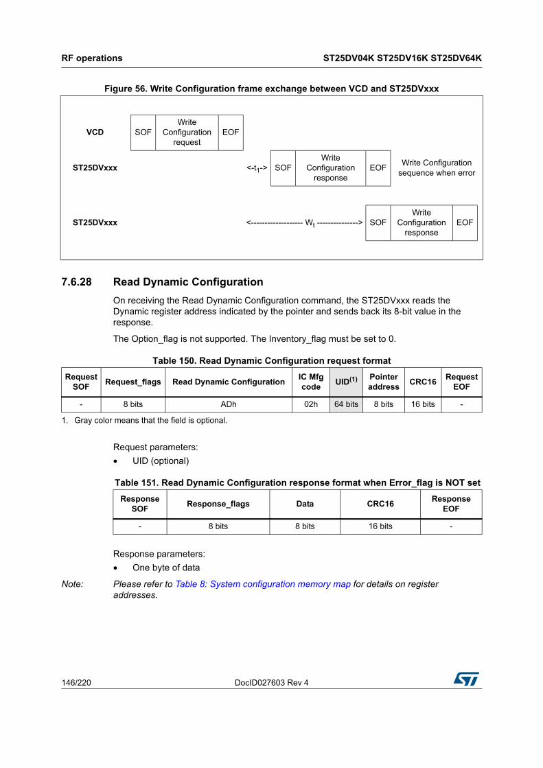
RF operations ST25DV04K ST25DV16K ST25DV64K
146/220 DocID027603 Rev 4
7.6.28 Read Dynamic Configuration
On receiving the Read Dynamic Configuration command, the ST25DVxxx reads the Dynamic register address indicated by the pointer and sends back its 8-bit value in the response.
The Option_flag is not supported. The Inventory_flag must be set to 0.
Request parameters:
• UID (optional)
Response parameters:
• One byte of data
Note: Please refer to Table 8: System configuration memory map for details on register addresses.
Figure 56. Write Configuration frame exchange between VCD and ST25DVxxx
VCD SOFWrite
Configuration request
EOF
ST25DVxxx <-t1-> SOFWrite
Configuration response
EOFWrite Configuration
sequence when error
ST25DVxxx <------------------- Wt ---------------> SOFWrite
Configuration response
EOF
Table 150. Read Dynamic Configuration request format
Request SOF
Request_flags Read Dynamic ConfigurationIC Mfg code
UID(1) Pointer address
CRC16Request
EOF
- 8 bits ADh 02h 64 bits 8 bits 16 bits -
1. Gray color means that the field is optional.
Table 151. Read Dynamic Configuration response format when Error_flag is NOT set
Response SOF
Response_flags Data CRC16Response
EOF
- 8 bits 8 bits 16 bits -

DocID027603 Rev 4 147/220
ST25DV04K ST25DV16K ST25DV64K RF operations
219
Response parameter:
• Error code as Error_flag is set
– 02h: command not recognized
– 03h: the option is not supported
– 0Fh: error with no information given
– 10h: block not available
7.6.29 Write Dynamic Configuration
On receiving the Write Dynamic Configuration command, the ST25DVxxx updates the Dynamic register addressed by the pointer.
The Option_flag is not supported. The Inventory_flag must be set to 0.
Request parameters:
• Request flags
• UID (optional)
• Pointer address
• Register value
Table 152. Read Dynamic Configuration response format when Error_flag is set
Response SOF
Response_flags Error code CRC16Response
EOF
- 8 bits 8 bits 16 bits -
Figure 57. Read Dynamic Configuration frame exchange between VCD and ST25DVxxx
VCD SOFRead Dynamic Configuration
requestEOF
ST25DVxxx <-t1-> SOFRead Dynamic Configuration
responseEOF
Table 153. Write Dynamic Configuration request format
Request SOF
Request_flagsWrite
Dynamic ConfigurationIC Mfg code
UID(1) Pointer address
Register Value
CRC16Request
EOF
- 8 bits AEh 02h64 bits
8 bits 8 bits 16 bits -
1. Gray color means that the field is optional.

RF operations ST25DV04K ST25DV16K ST25DV64K
148/220 DocID027603 Rev 4
Response parameter:
• No parameter. The response is sent back after t1.
Response parameter:
• Error code as Error_flag is set:
– 02h: command not recognized
– 03h: the option is not supported
– 0Fh: error with no information given
– 10h: block not available
7.6.30 Manage GPO
On receiving the Manage GPO command. Depending on the command argument, the ST25DV force the GPO output level if RF_USER interrupt is enabled, or send a pulse on GPO output if RF_INTERRUPT is enabled. If neither RF_USER nor RF_INTERRUPT was enabled, the command is not executed and ST25DVxxx responds an Error code “0F”.
The IT duration is defined by IT_TIME register and occurs just after the command response.
For the ST25DVxx-JF (CMOS output), a set means that the GPO pin is driven to a High level (VDCG) and a Reset pulls the GPO pin to a low level (VSS).
The IT corresponds to a transmission of a positive pulse on the GPO pin.
Table 154. Write Dynamic Configuration response format when Error_flag is NOT set
Response SOF Response_flags CRC16 Response EOF
- 8 bits 16 bits -
Table 155. Write Dynamic Configuration response format when Error_flag is set
Response SOF
Response_flags Error code CRC16Response
EOF
- 8 bits 8 bits 16 bits -
Figure 58. Write Dynamic Configuration frame exchange between VCD and ST25DVxxx
VCD SOFWrite Dynamic Configuration
request
EOF
ST25DVxxx <-t1-> SOFWrite Dynamic Configuration
responseEOF
Write Dynamic Configuration sequence
when no error
ST25DVxxx <-t1-> SOFWrite Dynamic Configuration
responseEOF
Write Dynamic Configuration sequence
when error
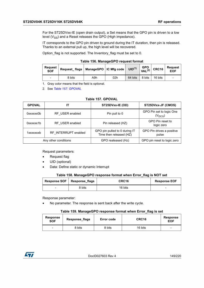
DocID027603 Rev 4 149/220
ST25DV04K ST25DV16K ST25DV64K RF operations
219
For the ST25DVxx-IE (open drain output), a Set means that the GPO pin is driven to a low level (VSS) and a Reset releases the GPO (High impedance).
IT corresponds to the GPO pin driven to ground during the IT duration, then pin is released. Thanks to an external pull up, the high level will be recovered.
Option_flag is not supported. The Inventory_flag must be set to 0.
Request parameters:
• Request flag
• UID (optional)
• Data: Define static or dynamic Interrupt
Response parameter:
• No parameter. The response is sent back after the write cycle.
Table 156. ManageGPO request format
Request SOF
Request_ flags ManageGPO IC Mfg code UID(1)
1. Gray color means that the field is optional.
GPOVAL(2)
2. See Table 157: GPOVAL
CRC16Request
EOF
- 8 bits A9h 02h 64 bits 8 bits 16 bits -
Table 157. GPOVAL
GPOVAL IT ST25DVxx-IE (OD) ST25DVxx-JF (CMOS)
0xxxxxx0b RF_USER enabled Pin pull to 0GPO Pin set to logic One
(VDCG)
0xxxxxx1b RF_USER enabled Pin released (HZ)GPO Pin reset to
logic zero
1xxxxxxxb RF_INTERRUPT enabledGPO pin pulled to 0 during IT
Time then released (HZ)GPO Pin drives a positive
pulse
Any other conditions GPO realeased (Hz) GPO pin reset to logic zero
Table 158. ManageGPO response format when Error_flag is NOT set
Response SOF Response_flags CRC16 Response EOF
- 8 bits 16 bits -
Table 159. ManageGPO response format when Error_flag is set
Response SOF
Response_flags Error code CRC16Response
EOF
- 8 bits 8 bits 16 bits -

RF operations ST25DV04K ST25DV16K ST25DV64K
150/220 DocID027603 Rev 4
Response parameter:
• Error code as Error_flag is set:
– 02h: command not recognized– 13h: the specified block was not successfully programmed (this error is generated
if the ManageCPO GPOVAL value is not in line with the GPO interrupts setting as specified in Table 157)
7.6.31 Write Message
On receiving the Write Message command, the ST25DVxxx puts the data contained in the request into the Mailbox buffer, update the MB_LEN_Dyn register, and set bit RF_PUT_MSG in MB_CTRL_Dyn register. It then reports if the write operation was successful in the response. The ST25DVxxx Mailbox contains up to 256 data bytes which are filled from the first location '00'. MSGlength parameter of the command is the number of Data bytes minus - 1 (00 for 1 byte of data, FFh for 256 bytes of data). Write Message could be executed only when Mailbox is accessible by RF (fast transfer mode is enabled, previous RF message was read or time-out occurs, no I2C message to be read). User can check it by reading b1 of MB_CTRL_Dyn “HOST_PUT_MSG” which must be reset to “0”. The Option_flag is not supported. (refer to Section 5.1: Fast transfer mode (FTM))
Request parameters:
• Request flags
• UID (optional)
• Message Length
• Message Data
Figure 59. ManageGPO frame exchange between VCD and ST25DVxxx
VCD SOF ManageGPO EOF
ST25DVxxx <-t1-> SOFManageGPO
responseEOF
ManageGPO sequence when error
Table 160. Write Message request format
Request SOF
Request_flags
Write Message
IC Mfg code UID(1) MSGLengthMessage
DataCRC16
Request EOF
- 8 bits AAh 02h 64 bits 1 byte(MSGLength + 1)
bytes16 bits -
1. Gray color means that the field is optional.
Table 161. Write Message response format when Error_flag is NOT set
Response SOF Response_flags CRC16 Response EOF
- 8 bits 16 bits -
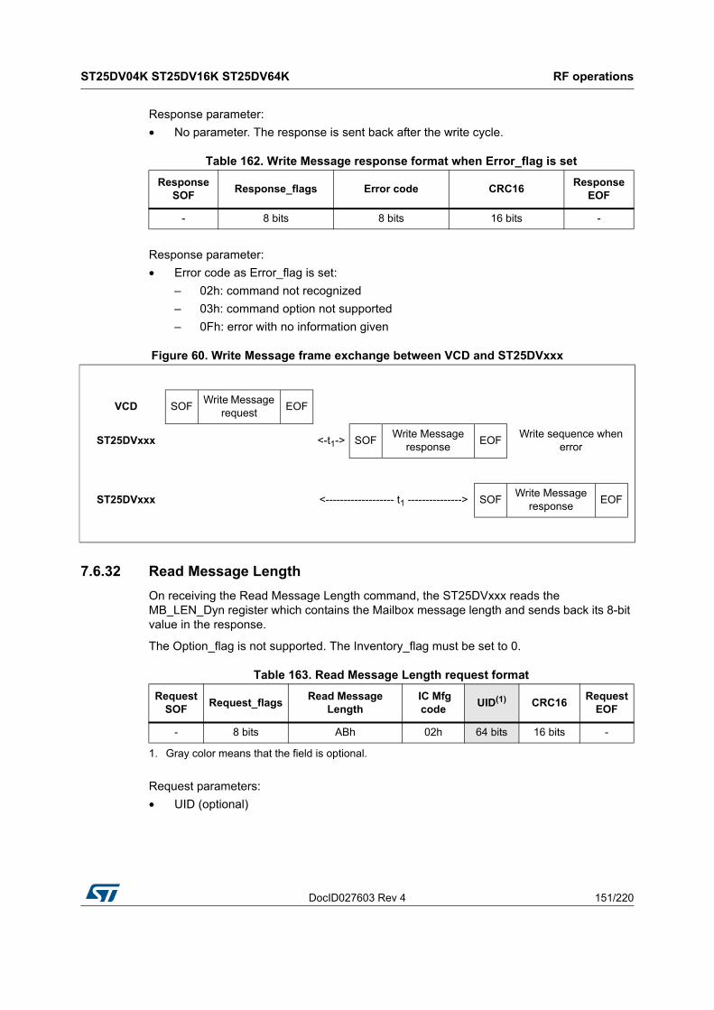
DocID027603 Rev 4 151/220
ST25DV04K ST25DV16K ST25DV64K RF operations
219
Response parameter:
• No parameter. The response is sent back after the write cycle.
Response parameter:
• Error code as Error_flag is set:
– 02h: command not recognized
– 03h: command option not supported
– 0Fh: error with no information given
7.6.32 Read Message Length
On receiving the Read Message Length command, the ST25DVxxx reads the MB_LEN_Dyn register which contains the Mailbox message length and sends back its 8-bit value in the response.
The Option_flag is not supported. The Inventory_flag must be set to 0.
Request parameters:
• UID (optional)
Table 162. Write Message response format when Error_flag is set
Response SOF
Response_flags Error code CRC16Response
EOF
- 8 bits 8 bits 16 bits -
Figure 60. Write Message frame exchange between VCD and ST25DVxxx
VCD SOFWrite Message
requestEOF
ST25DVxxx <-t1-> SOFWrite Message
responseEOF
Write sequence when error
ST25DVxxx <------------------- t1 ---------------> SOFWrite Message
responseEOF
Table 163. Read Message Length request format
Request SOF
Request_flagsRead Message
Length IC Mfg code
UID(1)
1. Gray color means that the field is optional.
CRC16Request
EOF
- 8 bits ABh 02h 64 bits 16 bits -

RF operations ST25DV04K ST25DV16K ST25DV64K
152/220 DocID027603 Rev 4
Response parameters:
• One byte of data: MB_LEN_Dyn register value
Response parameter:
• Error code as Error_flag is set
– 02h: command not recognized
– 03h: the option is not supported
– 0Fh: error given with no information
7.6.33 Read Message
On receiving the Read Message command, the ST25DVxxx reads up to 256 byte in the Mailbox from the location specified by MBpointer and sends back their value in the response. First MailBox location is '00’. When Number of bytes is set to 00h and MBPointer is equals to 00h, the MB_LEN bytes of the full message are returned. Otherwise, Read Message command returns (Number of Bytes + 1) bytes (i.e. 01h returns 2 bytes, FFh returns 256 bytes).
An error is reported if (Pointer + Nb of bytes + 1) is greater than the message length. RF Reading of the last byte of the mailbox message automatically clears b1 of MB_CTRL_Dyn “HOST_PUT_MSG”, and allows RF to put a new message.
The Option_flag is not supported. The Inventory_flag must be set to 0.
Table 164. Read Message Length response format when Error_flag is NOT set
Response SOF
Response_flags Data CRC16Response
EOF
- 8 bits 8 bits 16 bits -
Table 165. Read Message Length response format when Error_flag is set
Response SOF
Response_flags Error code CRC16Response
EOF
- 8 bits 8 bits 16 bits -
Figure 61. Read Message Length frame exchange between VCD and ST25DVxxx
VCD SOFRead Message Length request
EOF
ST25DVxxx <-t1-> SOFRead Message
Length responseEOF

DocID027603 Rev 4 153/220
ST25DV04K ST25DV16K ST25DV64K RF operations
219
Request parameters:
• Request flag
• UID (Optional)
• Pointer (start at 00h)
• Number of bytes is one less then the requested data
Response parameters:
• (number of data + 1 ) data bytes
Response parameter:
• Error code as Error_flag is set:
– 02h: command not recognized
– 03h: command option not supported
– 0Fh: error with no information given
7.6.34 Fast Read Message
On receiving the Fast Read Message command, the ST25DVxxx reads up to 256 byte in the Mailbox from the location specified by MBpointer and sends back their value in the response. First MailBox location is '00’. When Number of bytes is set to 00h and MBPointer is equals to 00h, the MB_LEN bytes of the full message are returned. Otherwise, Fast Read Message command returns (Number of Bytes + 1) bytes (i.e. 01h returns 2 bytes, FFh returns 256 bytes).
An error is reported if (Pointer + Nb of bytes + 1) is greater than the message length..
Table 166. Read Message request format
Request SOF
Request_flags
Read Message
IC Mfg code
UID(1)
1. Gray color means that the field is optional.
MBpointerNumber of Bytes
CRC16Request
EOF
- 8 bits ACh 02h 64 bits 8 bits 8 bits 16 bits -
Table 167. Read Message response format when Error_flag is NOT set
Response SOF
Response_flags Mailbox content CRC16Response
EOF
- 8 bits (Number of bytes + 1) bytes(1)
1. Number of message Bytes when Number of Bytes is set to 00h.
16 bits -
Figure 62. Read Message frame exchange between VCD and ST25DVxxx
VCD SOFRead Message
requestEOF
ST25DVxxx <-t1-> SOFRead Message
responseEOF

RF operations ST25DV04K ST25DV16K ST25DV64K
154/220 DocID027603 Rev 4
RF Reading of the last byte of mailbox message automatically clears b1 of MB_CTRL_Dyn “HOST_PUT_MSG” and allows RF to put a new message.
The data rate of the response is multiplied by 2 compated to Read Message.
The subcarrier_flag should be set to 0, otherwise the ST25DVxxx answers with an error code. The Option_flag is not supported, and the Inventory_flag must be set to 0.
Request parameters:
• Request flag
• UID (Optional)
• Pointer (start at 00h)
• Number of bytes is one less than the requested data
Response parameters:
• (number of bytes + 1) data bytes
Response parameter:
• Error code as Error_flag is set:
– 02h: command not recognized
– 03h: command option not supported
– 0Fh: error with no information given
7.6.35 Write Password
On receiving the Write Password command, the ST25DVxxx uses the data contained in the request to write the password and reports whether the operation was successful in the response. It is possible to modify a Password value only after issuing a valid Present password command (of the same password number). When the Option_flag is set, wait for EOF to respond. Refer to Section 5.6: Data Protection for details on password Management. The Inventory_flag must be set to 0.
During the RF write cycle time, Wt, there must be no modulation at all (neither 100% nor 10%), otherwise the ST25DVxxx may not correctly program the data into the memory.
The Wt time is equal to t1nom + N × 302 µs (N is an integer). After a successful write, the new value of the selected password is automatically activated. It is not required to present the new password value until the ST25DVxxx power-down.
Caution: If ST25DVxxx is powered through VCC, removing VCC or setting LPD high during Write Password command can abort the command. As a consequence, before writing a new password, RF user should check if VCC is ON, by reading EH_CTRL_Dyn register bit 3 (VCC_ON), and eventually ask host to maintain or to shut down VCC, and not to change
Figure 63. Fast Read Message frame exchange between VCD and ST25DVxxx
VCD SOFFast Read
Message requestEOF
ST25DVxxx <-t1-> SOFFast Read Message
responseEOF

DocID027603 Rev 4 155/220
ST25DV04K ST25DV16K ST25DV64K RF operations
219
voltage applied on LPD while issuing the Write Password command in order to avoid password corruption.
Request parameter:
• Request flags
• UID (optional)
• Password number:
– 00h = RF configuration password RF_PWD_0,
– 01h = RF_PWD_1,
– 02h = RF_PWD_2,
– 03h = RF_PWD_3,
– other = Error)
• Data
Response parameter:
• no parameter.
Response parameter:
• Error code as Error_flag is set:
– 02h: command not recognized
– 03h: command option not supported
– 10h: the password number is incorrect
– 12h: update right not granted, Present Password command not previously executed successfully
– 13h: the specified block was not successfully programmed
Table 168. Write Password request format
Request SOF
Request_flags
Write password
IC Mfg code
UID(1)
1. Gray color means that the field is optional.
Password number
Data CRC16Request
EOF
- 8 bits B1h 02h 64 bits 8 bits 64 bits 16 bits -
Table 169. Write Password response format when Error_flag is NOT set
Response SOF
Response_flags CRC16Response
EOF
- 8 bits 16 bits -
Table 170. Write Password response format when Error_flag is set
Response SOF
Response_flags Error code CRC16Response
EOF
- 8 bits 8 bits 16 bits -

RF operations ST25DV04K ST25DV16K ST25DV64K
156/220 DocID027603 Rev 4
7.6.36 Present Password
On receiving the Present Password command, the ST25DVxxx compares the requested password with the data contained in the request and reports if the operation has been successful in the response. Refer to Section 5.6: Data Protection for details on password Management. After a successful command, the security session associate to the password is open as described in Section 5.6: Data Protection.
The Option_flag is not supported, and the Inventory_flag must be set to 0.
Request parameter:
• Request flags
• UID (optional)
• Password Number (00h = Password configuration, 0x01 = Pswd1, 0x02 = Pswd2, 0x03 = Pswd3, other = Error)
• Password
Response parameter:
• No parameter. The response is sent back after the write cycle.
Figure 64. Write Password frame exchange between VCD and ST25DVxxx
VCD SOFWrite
Password request
EOF
ST25DVxxx <-t1-> SOFWrite
Password response
EOFWrite sequence
when error
ST25DVxxx <---------------- Wt -------------> SOFWrite
Password response
EOF
Table 171. Present Password request format
Request SOF
Request_flags
Present Password
IC Mfg code
UID(1)
1. Gray color means that the field is optional.
Password number
Password CRC16Request
EOF
- 8 bits B3h 02h 64 bits 8 bits 64 bits 16 bits -
Table 172. Present Password response format when Error_flag is NOT set
Response SOF
Response_flags CRC16Response
EOF
- 8 bits 16 bits -

DocID027603 Rev 4 157/220
ST25DV04K ST25DV16K ST25DV64K RF operations
219
Response parameter:
• Error code as Error_flag is set:
– 02h: command not recognized
– 03h: command option not supported
– 0Fh: the present password is incorrect
– 10h: the password number is incorrect
7.6.37 Fast Read Single Block
On receiving the Fast Read Single Block command, the ST25DVxxx reads the requested block and sends back its 32-bit value in the response. When the Option_flag is set, the response includes the Block Security Status. The data rate of the response is multiplied by 2.
The subcarrier_flag should be set to 0, otherwise the ST25DVxxx answers with an error code.
The Inventory_flag must be set to 0.
Block number is coded on 1 Byte and only first 256 blocks of ST25DV16K-xx and ST25DV64K-xx can be addressed using this command.
Table 173. Present Password response format when Error_flag is set
Response SOF
Response_flags Error code CRC16Response
EOF
- 8 bits 8 bits 16 bits -
Figure 65. Present Password frame exchange between VCD and ST25DVxxx
VCD SOFPresent
password request
EOF
ST25DVxxx <-t1-> SOFPresent
password response
EOF
Table 174. Fast Read Single Block request format
Request SOF
Request_flagsFast Read
Single BlockIC Mfg code
UID(1)
1. Gray color means that the field is optional.
Block number
CRC16Request
EOF
- 8 bits C0h 02h 64 bits 8 bits 16 bits -

RF operations ST25DV04K ST25DV16K ST25DV64K
158/220 DocID027603 Rev 4
Request parameters:
• Request flags
• UID (optional)
• Block number
Response parameters:
• Block security status if Option_flag is set (see Table 176: Block security status)
• Four bytes of block data
Response parameter:
• Error code as Error_flag is set:
– 02h: command not recognized
– 03h: command option not supported
– 0Fh: error with no information given
– 10h: the specified block is not available
– 15h: the specified block is read-protected
Table 175. Fast Read Single Block response format when Error_flag is NOT set
Response SOF
Response_flagsBlock security
status(1)
1. Gray color means that the field is optional.
Data CRC16Response
EOF
- 8 bits 8 bits 32 bits 16 bits -
Table 176. Block security status
b7 b6 b5 b4 b3 b2 b1 b0
Reserved for future useAll at 0
0: Current Block not locked
1: Current Block locked
Table 177. Fast Read Single Block response format when Error_flag is set
Response SOF
Response_flags Error code CRC16Response
EOF
- 8 bits 8 bits 16 bits -
Figure 66. Fast Read Single Block frame exchange between VCD and ST25DVxxx
VCD SOFFast Read Single
Block requestEOF
ST25DVxxx <-t1-> SOFFast Read Single Block response
EOF

DocID027603 Rev 4 159/220
ST25DV04K ST25DV16K ST25DV64K RF operations
219
7.6.38 Fast Extended Read Single Block
On receiving the Fast Extended Read Single Block command, the ST25DVxxx reads the requested block and sends back its 32-bit value in the response. When the Option_flag is set, the response includes the Block Security Status. The data rate of the response is multiplied by 2.
The subcarrier_flag should be set to 0, otherwise the ST25DVxxx answers with an error code.
The Inventory_flag must be set to 0.
Block number is coded on 2 Bytes so all memory blocks of ST25DV16K-xx and ST25DV64K-xx can be addressed using this command
Request parameters:
• Request flags
• UID (optional)
• Block number
Response parameters:
• Block security status if Option_flag is set (see Table 176: Block security status)
• Four bytes of block data
Table 178. Fast Extended Read Single Block request format
Request SOF
Request_flags
Fast Extended
Read Single Block
IC Mfg code
UID(1)
1. Gray color means that the field is optional.
Block number
CRC16Request
EOF
- 8 bits C4h 02h 64 bits 16 bits 16 bits -
Table 179. Fast Extended Read Single Block response format when Error_flag is NOT set
Response SOF
Response_flagsBlock security
status(1)
1. Gray color means that the field is optional.
Data CRC16Response
EOF
- 8 bits 8 bits 32 bits 16 bits -
Table 180. Block security status
b7 b6 b5 b4 b3 b2 b1 b0
Reserved for future useAll at 0
0: Current Block not locked
1: Current Block locked

RF operations ST25DV04K ST25DV16K ST25DV64K
160/220 DocID027603 Rev 4
Response parameter:
• Error code as Error_flag is set:
– 02h: command not recognized
– 03h: command option not supported
– 0Fh: error with no information given
– 10h: the specified block is not available
– 15h: the specified block is read-protected
7.6.39 Fast Read Multiple Blocks
On receiving the Fast Read Multiple Blocks command, the ST25DVxxx reads the selected blocks and sends back their value in multiples of 32 bits in the response. The blocks are numbered from 00h up to the last block of user memory in the request, and the value is minus one (–1) in the field. For example, if the “Number of blocks” field contains the value 06h, seven blocks are read. The maximum number of blocks is fixed to 256 assuming that they are all located in the same area. If the number of blocks overlaps area or overlaps the end of user memory, the ST25DVxxx returns an error code.
When the Option_flag is set, the response includes the Block Security Status. The data rate of the response is multiplied by 2.
The subcarrier_flag should be set to 0, otherwise the ST25DVxxx answers with an error code.
The Inventory_flag must be set to 0.
Block number is coded on 1 Byte and only first 256 blocks of ST25DV16K-xx and ST25DV64K-xx can be addressed using this command.
Table 181. Fast Extended Read Single Block response format when Error_flag is set
Response SOF
Response_flags Error code CRC16Response
EOF
- 8 bits 8 bits 16 bits -
Figure 67. Fast Extended Read Single Block frame exchange between VCD and ST25DVxxx
VCD SOFFast Extended Read Single Block request
EOF
ST25DVxxx <-t1-> SOFFast Extended
Read Single Block response
EOF

DocID027603 Rev 4 161/220
ST25DV04K ST25DV16K ST25DV64K RF operations
219
Request parameters:
• Request flag
• UID (Optional)
• First block number
• Number of blocks
Response parameters:
• Block security status if Option_flag is set (see Table 184: Block security status if Option_flag is set)
• N block of data
Response parameter:
• Error code as Error_flag is set:
– 02h: command not recognized
– 0Fh: error with no information given
– 03h: the option is not supported
– 10h: block address not available
– 15h: block read-protected
Table 182. Fast Read Multiple Block request format
Request SOF
Request_flags
Fast Read Multiple Block
IC Mfg code
UID(1)
1. Gray color means that the field is optional.
First block
number
Number of
blocksCRC16
Request EOF
- 8 bits C3h 02h 64 bits 8 bits 8 bits 16 bits -
Table 183. Fast Read Multiple Block response format when Error_flag is NOT set
Response SOF
Response_flagsBlock security
status(1)
1. Gray color means that the field is optional.
Data CRC16Response
EOF
- 8 bits 8 bits(2)
2. Repeated as needed.
32 bits(2) 16 bits -
Table 184. Block security status if Option_flag is set
b7 b6 b5 b4 b3 b2 b1 b0
Reserved for future use All at 0
0: Current not locked 1: Current locked
Table 185. Fast Read Multiple Block response format when Error_flag is set
Response SOF Response_flags Error code CRC16 Response EOF
- 8 bits 8 bits 16 bits -

RF operations ST25DV04K ST25DV16K ST25DV64K
162/220 DocID027603 Rev 4
7.6.40 Fast Extended Read Multiple Block
On receiving the Fast Extended Read Multiple Block command, the ST25DVxxx reads the selected blocks and sends back their value in multiples of 32 bits in the response. The blocks are numbered from 00h to up to the last block of memory in the request and the value is minus one (–1) in the field. For example, if the “Number of blocks” field contains the value 06h, seven blocks are read. The maximum number of blocks is fixed to 2047 assuming that they are all located in the same area. If the number of blocks overlaps several areas or overlaps the end of user memory, the ST25DVxxx returns an error code.
When the Option_flag is set, the response includes the Block Security Status. The data rate of the response is multiplied by 2.
The subcarrier_flag should be set to 0, otherwise the ST25DVxxx answers with an error code.
The Inventory_flag must be set to 0.
Block number is coded on 2 Bytes so all memory blocks of ST25DV16K-xx and ST25DV64K-xx can be addressed using this command.
Request parameters:
• Request flag
• UID (Optional)
• First block number
• Number of blocks
Figure 68. Fast Read Multiple Block frame exchange between VCD and ST25DVxxx
VCD SOFFast Read
Multiple Block request
EOF
ST25DVxxx <-t1-> SOFFast Read
Multiple Block response
EOF
Table 186. Fast Extended Read Multiple Block request format
Request SOF
Request_flags
Fast Extended
Read Multiple Block
IC Mfg code
UID(1)
1. Gray color means that the field is optional.
First block
number
Block Number
CRC16Request
EOF
- 8 bits C5h 02h 64 bits 16 bits 16 bits 16 bits -

DocID027603 Rev 4 163/220
ST25DV04K ST25DV16K ST25DV64K RF operations
219
Response parameters:
• Block security status if Option_flag is set (see Table 184: Block security status if Option_flag is set)
• N block of data
Response parameter:
• Error code as Error_flag is set:
– 02h: command not recognized
– 03h: the option is not supported
– 0Fh: error with no information given
– 10h: block address not available
– 15h: block read-protected
Table 187. Fast Extended Read Multiple Block response format when Error_flag is NOT set
Response SOF
Response_flagsBlock security
status(1)
1. Gray color means that the field is optional.
Data CRC16Response
EOF
- 8 bits 8 bits(2)
2. Repeated as needed.
32 bits(2) 16 bits -
Table 188. Block security status if Option_flag is set
b7 b6 b5 b4 b3 b2 b1 b0
Reserved for future use All at 0
0: Current not locked 1: Current locked
Table 189. Fast Read Multiple Block response format when Error_flag is set
Response SOF Response_flags Error code CRC16 Response EOF
- 8 bits 8 bits 16 bits -
Figure 69. Fast Extended Read Multiple Block frame exchange between VCD and ST25DVxxx
VCD SOFFast Extended Read Multiple Block request
EOF
ST25DVxxx <-t1-> SOFFast Extended Read Multiple
Block responseEOF

RF operations ST25DV04K ST25DV16K ST25DV64K
164/220 DocID027603 Rev 4
7.6.41 Fast Write Message
On receiving the Fast Write Message command, the ST25DVxxx puts the data contained in the request into the mailbox buffer, updates the Message Length register MB_LEN_Dyn, and set Mailbox loaded bit RF_PUT_MSG. It then reports if the write operation was successful in the response. The ST25DVxxx mailbox contains up to 256 data bytes which are filled from the first location '00'. MSGlength parameter of the command is the number of Data bytes minus - 1 (00 for 1 byte of data, FFh for 256 bytes of data). Fast Write Message can be executed only when Mailbox is accessible by RF (previous RF message was read or time-out occurs, no I2C message to be read). User can check it by reading b1 of MB_CTRL_Dyn “HOST_PUT_MSG”, which must be reset to “0”. (refer to Section 5.1: Fast transfer mode (FTM)).
• The data rate of the response is multiplied by 2 compared to Write Message command.
• The Option_flag is not supported.
• The Inventory_flag must be set to 0.
• The subcarrier_flag should be set to 0, otherwise the ST25DVxxx answers with an error code.
Request parameters:
• Request flag
• UID (optional)
• Message Lenght
• Message Data
Response parameters:
• No parameter. The response is sent back after the write cycle.
Table 190. Fast Write Message request format
Request SOF
Request_flags
Fast Write Message
IC Mfg code
UID(1) MSGLength Message Data CRC16Request
EOF
- 8 bits CAh 02h 64 bits 1 byte (MsgLenght + 1) bytes 16 bits -
1. Gray color means that the field is optional.
Table 191. Fast Write Message response format when Error_flag is NOT set
Response SOF Response_flags CRC16 Response EOF
- 8 bits 16 bits -
Table 192. Fast Write Message response format when Error_flag is set
Response SOF Response_flags CRC16 Response EOF
- 8 bits 8 bits 16 bits

DocID027603 Rev 4 165/220
ST25DV04K ST25DV16K ST25DV64K RF operations
219
Response parameter:
• Error code as Error_flag is set:
– 02h: command not recognized
– 03h: command option not supported
– 0Fh: error with no information given
7.6.42 Fast Read Message Length
On receiving the Fast Read Message Length command, the ST25DV reads the MB_LEN_dyn register which contains the mailbox message length and sends back its 8-bit value in the response.
The Option_flag is not supported. The Inventory_flag must be set to 0.
The subcarrier_flag should be set to 0, otherwise the ST25DVxxx answers with an error code.
The data rate of the response is multiplied by 2 compared to Read Message Length command.
Request parameters:
• Request flag
• UID (optional)
Figure 70. Fast Write Message frame exchange between VCD and ST25DVxxx
VCD SOFFast WriteMessagerequest
EOF
ST25DVxxx <-t1-> SOFFast Write Message
rresponse0EOF
Write sequence when error
ST25DVxxx <------------------- t1 ---------------> SOFFast Write Message
r responseEOF
Table 193. Fast Read Message Length request format
Request SOF
Request_flagsFast Read
Message LengthIC Mfg code
UID(1)
1. Gray color means that the field is optional.
CRC16Request
EOF
- 8 bits CBh 02h 64 bits 16 bits -

RF operations ST25DV04K ST25DV16K ST25DV64K
166/220 DocID027603 Rev 4
Response parameters:
• One byte of data: volatile Control register.
Response parameter:
• Error code as Error_flag is set:
– 02h: command option not recognized– 03h: command not supported
– 0Fh: error with no information given
7.6.43 Fast Read Dynamic Configuration
On receiving the Fast Read Dynamic Configuration command, the ST25DVxxx reads the Dynamic register address by the pointer and sends back its 8-bit value in the response.
The Option_flag is not supported. The Inventory_flag must be set to 0.
The subcarrier_flag should be set to 0, otherwise the ST25DVxxx answers with an error code.
The data rate of the response is multiplied by 2 compared to Read Dynamic Configuration command.
Table 194. Fast Read Message Length response format when Error_flag is NOT set
Response SOF Response_flags Data CRC16 Response EOF
- 8 bits 8 bits 16 bits -
Table 195. Fast Read Message Length response format when Error_flag is set
Response SOF Response_flags Error code CRC16 Response EOF
- 8 bits 8 bits 16 bits -
Figure 71. Fast Read Message Length frame exchange between VCD and ST25DVxxx
VCD SOFFast Read
Message Length request
EOF
ST25DVxxx <-t1-> SOFFast Read
Message Lengthrequest
EOF
Table 196. Fast Read Dynamic Configuration request format
Request SOF
Request_flagsFast Read Dynamic
ConfigurationIC Mfg code
UID(1) Pointer address
CRC16Request
EOF
- 8 bits CDh 02h 64 bits 8 bits 16 bits -
1. Gray color means that the field is optional.
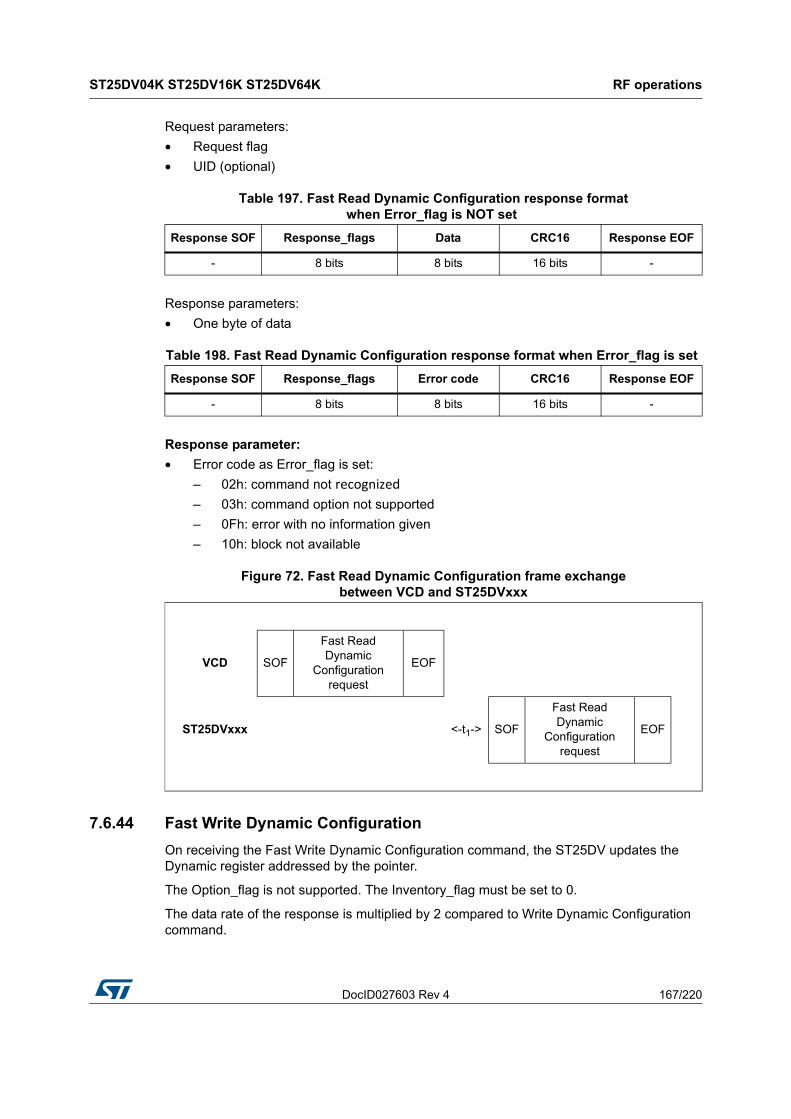
DocID027603 Rev 4 167/220
ST25DV04K ST25DV16K ST25DV64K RF operations
219
Request parameters:
• Request flag
• UID (optional)
Response parameters:
• One byte of data
Response parameter:
• Error code as Error_flag is set:
– 02h: command not recognized– 03h: command option not supported
– 0Fh: error with no information given
– 10h: block not available
7.6.44 Fast Write Dynamic Configuration
On receiving the Fast Write Dynamic Configuration command, the ST25DV updates the Dynamic register addressed by the pointer.
The Option_flag is not supported. The Inventory_flag must be set to 0.
The data rate of the response is multiplied by 2 compared to Write Dynamic Configuration command.
Table 197. Fast Read Dynamic Configuration response format when Error_flag is NOT set
Response SOF Response_flags Data CRC16 Response EOF
- 8 bits 8 bits 16 bits -
Table 198. Fast Read Dynamic Configuration response format when Error_flag is set
Response SOF Response_flags Error code CRC16 Response EOF
- 8 bits 8 bits 16 bits -
Figure 72. Fast Read Dynamic Configuration frame exchange between VCD and ST25DVxxx
VCD SOF
Fast Read Dynamic
Configuration request
EOF
ST25DVxxx <-t1-> SOF
Fast Read Dynamic
Configuration request
EOF

RF operations ST25DV04K ST25DV16K ST25DV64K
168/220 DocID027603 Rev 4
Request parameters:
• Request flag
• UID (optional)
• Pointer address
• Register value
Response parameters:
• No parameter. The response is sent back after t1.
Response parameter:
• Error code as Error_flag is set:
– 02h: command not recognized– 03h: command option not supported
– 0Fh: error with no information given
– 10h: block not available
Table 199. Fast Write Dynamic Configuration request format
Request SOF
Request_flagsFast Write Dynamic
ConfigurationIC Mfg code
UID(1) Pointer address
Register Value
CRC16Request
EOF
- 8 bits CEh 02h 64 bits 8 bits 8 bits 16 bits -
1. Gray color means that the field is optional.
Table 200. Fast Write Dynamic Configuration response format when Error_flag is NOT set
Response SOF Response_flags CRC16 Response EOF
- 8 bits 16 bits -
Table 201. Fast Write Dynamic Configuration response format when Error_flag is set
Response SOF Response_flags Error code CRC16 Response EOF
- 8 bits 8 bits 16 bits -
Figure 73. Fast Write Dynamic Configuration frame exchange between VCD and ST25DVxxx
VCD SOF
Fast Write Dynamic
Configuration request
EOF
ST25DVxxx <-t1-> SOF
Fast Write Dynamic
Configuration request
EOF
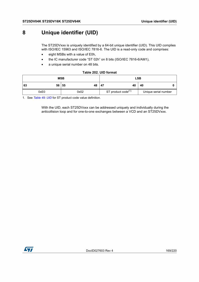
DocID027603 Rev 4 169/220
ST25DV04K ST25DV16K ST25DV64K Unique identifier (UID)
219
8 Unique identifier (UID)
The ST25DVxxx is uniquely identified by a 64-bit unique identifier (UID). This UID complies with ISO/IEC 15963 and ISO/IEC 7816-6. The UID is a read-only code and comprises:
• eight MSBs with a value of E0h,
• the IC manufacturer code “ST 02h” on 8 bits (ISO/IEC 7816-6/AM1),
• a unique serial number on 48 bits.
With the UID, each ST25DVxxx can be addressed uniquely and individually during the anticollision loop and for one-to-one exchanges between a VCD and an ST25DVxxx.
Table 202. UID format
MSB LSB
63 56 55 48 47 40 40 0
0xE0 0x02 ST product code(1) Unique serial number
1. See Table 49: UID for ST product code value definition.

Device parameters ST25DV04K ST25DV16K ST25DV64K
170/220 DocID027603 Rev 4
9 Device parameters
9.1 Maximum rating
Stressing the device above the rating listed in Table 203: Absolute maximum ratings may cause permanent damage to the device. These are stress ratings only and operation of the device, at these or any other conditions above those indicated in the operating sections of this specification, is not implied. Exposure to absolute maximum rating conditions for extended periods may affect the device reliability. Device mission profile (application conditions) is compliant with JEDEC JESD47 qualification standard. Extended mission profiles can be assessed on demand.
Refer also to the STMicroelectronics SURE Program and other relevant quality documents.
Table 203. Absolute maximum ratings
Symbol Parameter Min.Max.
Unit
TAAmbient operating temperature
Range 6 All packagesRF and I2C interfaces
-40 85 °C
Range 8
UFDFPN8, UFDFPN12
RF and I2C interfaces
- 40 105 °C
SO8N, TSSOPRF interface - 40 105 °C
I2C interface - 40 125 °C
TSTG Storage Temperature Sawn wafer on UV tape kept in its original packing form
15 25 °C
tSTG Retain - 9(1) months
TSTG Storage temperatureUFDFPN8 (MLP8),SO8N, TSSOP8, UFDFPN12, WLCSP10
- 65 150 °C
TLEAD Lead temperature during soldering see note (2) °C
VIO I2C input or output range - 0.50 6.5 V
VDCG Supply GPO CMOS driver - 0.50 6.5 V
VCC I2C supply voltage - 0.50 6.5 V
IOL_MAX_SDA DC output current on pin SDA (when equal to 0) - 5 mA
IOL_MAX_GPO_OD DC output current on pin GPO open drain (when equal to 0) - 1.5 mA
VMAX_1(3) RF input voltage amplitude peak to peak between AC0
and AC1, VSS pin left floatingVAC0 - VAC1 - 11 V
VMAX_2(3) AC voltage between AC0 and VSS, or AC1 and VSS
VAC0 - VSS, or VAC1 - VSS
- 0.50 5.5 V
VESD Electrostatic discharge voltage (human body model)(4) All pins 2000 - V
1. Counted from ST production date.
2. Compliant with JEDEC Std J-STD-020C (for small body, Sn-Pb or Pb assembly), the ST ECOPACK® 7191395 specification, and the European directive on Restrictions on Hazardous Substances (RoHS) 2002/95/EU.
3. Based on characterization, not tested in production.
4. AEC-Q100-002 (compliant with JEDEC Std JESD22-A114, C1 = 100 pF, R1 = 1500 Ω, R2 = 500 Ω)
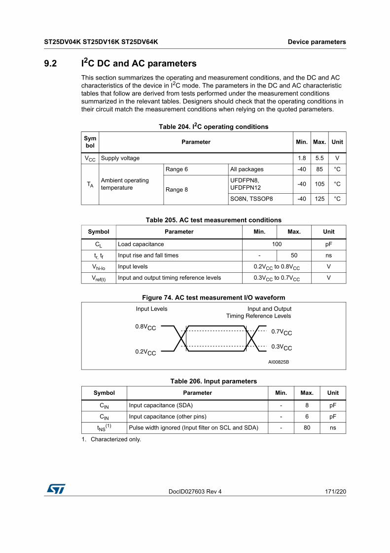
DocID027603 Rev 4 171/220
ST25DV04K ST25DV16K ST25DV64K Device parameters
219
9.2 I2C DC and AC parameters
This section summarizes the operating and measurement conditions, and the DC and AC characteristics of the device in I2C mode. The parameters in the DC and AC characteristic tables that follow are derived from tests performed under the measurement conditions summarized in the relevant tables. Designers should check that the operating conditions in their circuit match the measurement conditions when relying on the quoted parameters.
Figure 74. AC test measurement I/O waveform
Table 204. I2C operating conditions
Symbol
Parameter Min. Max. Unit
VCC Supply voltage 1.8 5.5 V
TAAmbient operating temperature
Range 6 All packages -40 85 °C
Range 8
UFDFPN8, UFDFPN12
-40 105 °C
SO8N, TSSOP8 -40 125 °C
Table 205. AC test measurement conditions
Symbol Parameter Min. Max. Unit
CL Load capacitance 100 pF
tr, tf Input rise and fall times - 50 ns
Vhi-lo Input levels 0.2VCC to 0.8VCC V
Vref(t) Input and output timing reference levels 0.3VCC to 0.7VCC V
Table 206. Input parameters
Symbol Parameter Min. Max. Unit
CIN Input capacitance (SDA) - 8 pF
CIN Input capacitance (other pins) - 6 pF
tNS(1)
1. Characterized only.
Pulse width ignored (Input filter on SCL and SDA) - 80 ns

Device parameters ST25DV04K ST25DV16K ST25DV64K
172/220 DocID027603 Rev 4
Table 207. I2C DC characteristics up to 85°C
Symbol Parameter Test condition Min. Typ. Max. Unit
ILIInput leakage current
(SCL, SDA)VIN = VSS or VCC
device in Standby mode- 0.03 ± 0.1 µA
ILIInput leakage current
(LPD)VIN = VSS
device in Standby mode- 0.1 ± 0.5 µA
ILOOutput leakage current
(SDA)
SDA in Hi-Z, external voltage
applied on SDA: VSS or VCC
- 0.03 ± 0.1 µA
ICC_E2Operating Supply
current (Device select E2 Address) Read(1)
VCC = 1.8 V, fC = 1MHz(rise/fall time < 50 ns)
- 116 160
µAVCC = 3.3 V, fC = 1MHz
(rise/fall time < 50 ns)- 220 240
VCC = 5.5 V, fC = 1MHz
(rise/fall time < 50 ns)- 510 550
ICC_MBOperating Supply
current (Device select MB Address) Read(1)
VCC = 1.8 V, fC = 1MHz(rise/fall time < 50 ns)
- 116 160
µAVCC = 3.3 V, fC = 1MHz(rise/fall time < 50 ns)
- 220 240
VCC = 5.5 V, fC = 1MHz
(rise/fall time < 50 ns)- 510 550
ICC0
Operating Supply current (Device select E2 Address) Write(1)
VCC = 1.8 V, fC = 1MHz(rise/fall time < 50 ns)
- 110 300
µAVCC = 3.3 V, fC = 1MHz
(rise/fall time < 50 ns)- 110 330
VCC = 5.5 V, fC = 1MHz
(rise/fall time < 50 ns)- 130 430
ICC0_MBOperating Supply
current (Device select MB Address) Write(1)
VCC = 1.8 V, fC = 1MHz(rise/fall time < 50 ns)
- 170 200
µAVCC = 3.3 V, fC = 1MHz(rise/fall time < 50 ns)
- 280 300
VCC = 5.5 V, fC = 1MHz(rise/fall time < 50 ns)
- 520 600
ICC1(LPD = 1)
Low Power Down supply current
VCC = 1.8 V - 0.84 1.5
µAVCC = 3.3 V - 1.3 2
VCC = 5.5 V - 1.7 3
ICC1_PON(LPD = 0)
Static Standby supply current after power ON or device select stop
or time out
VCC = 1.8 V - 72 100
µAVCC = 3.3 V - 76 100
VCC = 5.5 V - 87 120

DocID027603 Rev 4 173/220
ST25DV04K ST25DV16K ST25DV64K Device parameters
219
VILInput low voltage
(SDA, SCL)
VCC = 1.8 V - 0.45 - 0.25 VCC
VVCC = 3.3 V - 0.45 - 0.3 VCC
VCC = 5.5 V - 0.45 - 0.3 VCC
VIL_LPD Input low voltage (LPD) VCC = 3.3 V - 0.45 - 0.2 VCC V
VIHInput high voltage
(SDA, SCL)
VCC = 1.8 V 0.75 VCC - VCC + 1
VVCC = 3.3 V 0.75 VCC - VCC + 1
VCC = 5.5 V 0.75 VCC - VCC + 1
VIH_LPDInput high voltage
(LPD)
VCC = 1.8 V 0.85 VCC - VCC + 1
VVCC = 3.3 V 0.85 VCC - VCC + 1
VCC = 5.5 V 0.85 VCC - VCC + 1
VOL_SDAOutput low voltage
SDA (1 MHz)
IOL = 1 mA, VCC = 1.8 V - 0.05 0.4
VIOL = 2.1 mA, VCC = 3.3 V - 0.075 0.4
IOL = 3 mA, VCC = 5.5 V - 0.09 0.4
VCC_Power_upDevice Select Acknowledge
fC = 100 KHz - 1.48 1.7 V
1. SCL, SDA connected to Ground or VCC. SDA connected to VCC through a pull-up resistor.
Table 207. I2C DC characteristics up to 85°C (continued)
Symbol Parameter Test condition Min. Typ. Max. Unit

Device parameters ST25DV04K ST25DV16K ST25DV64K
174/220 DocID027603 Rev 4
Table 208. I2C DC characteristics up to 125°C
Symbol Parameter Test condition Min. Typ. Max. Unit
ILIInput leakage current
(SCL, SDA)VIN = VSS or VCC
device in Standby mode- 0.03 ± 0.1 µA
ILIInput leakage current
(LPD)VIN = VSS
device in Standby mode- 0.1 ± 0.5 µA
ILOOutput leakage current
(SDA)
SDA in Hi-Z, external voltage
applied on SDA: VSS or VCC
- 0.03 ± 0.1 µA
ICC_E2Operating Supply
current (Device select E2 Address) Read(1)
VCC = 1.8 V, fC = 1MHz(rise/fall time < 50 ns)
- 126 180
µAVCC = 3.3 V, fC = 1MHz(rise/fall time < 50 ns)
- 230 260
VCC = 5.5 V, fC = 1MHz(rise/fall time < 50 ns)
- 510 550
ICC_MBOperating Supply
current (Device select MB Address) Read(1)
VCC = 1.8 V, fC = 1MHz(rise/fall time < 50 ns)
- 126 180
µAVCC = 3.3 V, fC = 1MHz(rise/fall time < 50 ns)
- 230 260
VCC = 5.5 V, fC = 1MHz(rise/fall time < 50 ns)
- 510 550
ICC0
Operating Supply current (Device select E2 Address) Write(1)
VCC = 1.8 V, fC = 1MHz(rise/fall time < 50 ns)
- 120 310
µAVCC = 3.3 V, fC = 1MHz(rise/fall time < 50 ns)
- 120 350
VCC = 5.5 V, fC = 1MHz(rise/fall time < 50 ns)
- 140 450
ICC0_MBOperating Supply
current (Device select MB Address) Write(1)
VCC = 1.8 V, fC = 1MHz(rise/fall time < 50 ns)
- 180 220
µAVCC = 3.3 V, fC = 1MHz(rise/fall time < 50 ns)
- 290 320
VCC = 5.5 V, fC = 1MHz(rise/fall time < 50 ns)
- 520 600
ICC1(LPD = 1)
Low Power Down supply current
VCC = 1.8 V - 2.5 5
µAVCC = 3.3 V - 3 6
VCC = 5.5 V - 4 7
ICC1_PON(LPD = 0)
Static Standby supply current after power ON or device select stop
or time out
VCC = 1.8 V - 78 110
µAVCC = 3.3 V - 82 110
VCC = 5.5 V - 95 130
VILInput low voltage
(SDA, SCL)
VCC = 1.8 V - 0.45 - 0.25 VCC
VVCC = 3.3 V - 0.45 - 0.3 VCC
VCC = 5.5 V - 0.45 - 0.3 VCC

DocID027603 Rev 4 175/220
ST25DV04K ST25DV16K ST25DV64K Device parameters
219
VIL_LPD Input low voltage (LPD) VCC = 3.3 V - 0.45 - 0.2 VCC V
VIHInput high voltage
(SDA, SCL)
VCC = 1.8 V 0.75 VCC - VCC + 1
VVCC = 3.3 V 0.75 VCC - VCC + 1
VCC = 5.5 V 0.75 VCC - VCC + 1
VIH_LPDInput high voltage
(LPD)
VCC = 1.8 V 0.85 VCC - VCC + 1
VVCC = 3.3 V 0.85 VCC - VCC + 1
VCC = 5.5 V 0.85 VCC - VCC + 1
VOL_SDAOutput low voltage
SDA (1 MHz)
IOL = 1 mA, VCC = 1.8 V - 0.05 0.4
VIOL = 2.1 mA, VCC = 3.3 V - 0.08 0.4
IOL = 3 mA, VCC = 5.5 V - 0.1 0.4
VCC_Power_upDevice Select Acknowledge
fC = 100 KHz - 1.48 1.7 V
1. SCL, SDA connected to Ground or VCC. SDA connected to VCC through a pull-up resistor.
Table 208. I2C DC characteristics up to 125°C (continued)
Symbol Parameter Test condition Min. Typ. Max. Unit

Device parameters ST25DV04K ST25DV16K ST25DV64K
176/220 DocID027603 Rev 4
Table 209. I2C AC characteristics up to 85°C
Test conditions specified in Table 204
Symbol Alt. Parameter Min. Max. Unit
fC fSCL Clock frequency 0.05 1000 kHz
tCHCL tHIGH Clock pulse width high 0.26 25000(1) µs
tCLCH tLOW Clock pulse width low 0.5 25000(2) µs
tSTART_OUT - I²C timeout on Start condition 35 - ms
tXH1XH2 tR Input signal rise time (3) (3) ns
tXL1XL2 tF Input signal fall time (3) (3) ns
tDL1DL2(4) tF SDA (out) fall time 20 120 ns
tDXCX tSU:DAT Data in set up time 0 - ns
tCLDX tHD:DAT Data in hold time 0 - ns
tCLQX(5) tDH Data out hold time 100 - ns
tCLQV(6) tAA Clock low to next data valid (access time) - 450 ns
tCHDX(7) tSU:STA Start condition set up time 250 - ns
tDLCL tHD:STA Start condition hold time 0.25 35000(8) µs
tCHDH tSU:STO Stop condition set up time 250 - ns
tDHDL tBUF Time between Stop condition and next Start condition 500 - ns
tW - I²C write time(9) - 5 ms
tbootDC - RF OFF and LPD = 0 - 0.6 ms
tbootLPD - RF OFF - 0.6 ms
1. tCHCL timeout.
2. tCLCH timeout.
3. There is no min. or max. values for the input signal rise and fall times. It is however recommended by the I2C specification that the input signal rise and fall times be less than 120 ns when fC < 1 MHz.
4. Characterized on bench.
5. To avoid spurious Start and Stop conditions, a minimum delay is placed between SCL=1 and the falling or rising edge of SDA.
6. tCLQV is the time (from the falling edge of SCL) required by the SDA bus line to reach 0.8VCC in a compatible way with the I2C specification (which specifies tSU:DAT (min) = 100 ns), assuming that the Rbus × Cbus time constant is less than 150 ns (as specified in the Figure 76: I2C Fast mode (fC = 1 MHz): maximum Rbus value versus bus parasitic capacitance (Cbus)).
7. For a reStart condition, or following a write cycle.
8. tDLCL timeout.
9. I2C write time for 1 Byte, 2 Bytes, 3 Bytes or 4 Bytes in EEPROM (user memory and system configuration), provided they are all located in the same memory page, that is the most significant memory address bits (b16-b2) are the same.

DocID027603 Rev 4 177/220
ST25DV04K ST25DV16K ST25DV64K Device parameters
219
Table 210. I2C AC characteristics up to 125°C
Test conditions specified in Table 204
Symbol Alt. Parameter Min. Max. Unit
fC fSCL Clock frequency 0.05 1000 kHz
tCHCL tHIGH Clock pulse width high 0.26 25000(1) µs
tCLCH tLOW Clock pulse width low 0.5 25000(2) µs
tSTART_OUT - I²C timeout on Start condition 35 - ms
tXH1XH2 tR Input signal rise time (3) (3) ns
tXL1XL2 tF Input signal fall time (3) (3) ns
tDL1DL2(4) tF SDA (out) fall time 20 120 ns
tDXCX tSU:DAT Data in set up time 0 - ns
tCLDX tHD:DAT Data in hold time 0 - ns
tCLQX(5) tDH Data out hold time 100 - ns
tCLQV(6) tAA Clock low to next data valid (access time) - 450 ns
tCHDX(7) tSU:STA Start condition set up time 250 - ns
tDLCL tHD:STA Start condition hold time 0.25 35000(8) µs
tCHDH tSU:STO Stop condition set up time 250 - ns
tDHDL tBUF Time between Stop condition and next Start condition 500 - ns
tW - I²C write time(9) - 5.5 ms
tbootDC - RF OFF and LPD = 0 - 0.6 ms
tbootLPD - RF OFF - 0.6 ms
1. tCHCL timeout.
2. tCLCH timeout.
3. There is no min. or max. values for the input signal rise and fall times. It is however recommended by the I2C specification that the input signal rise and fall times be less than 120 ns when fC < 1 MHz.
4. Characterized on bench.
5. To avoid spurious Start and Stop conditions, a minimum delay is placed between SCL=1 and the falling or rising edge of SDA.
6. tCLQV is the time (from the falling edge of SCL) required by the SDA bus line to reach 0.8VCC in a compatible way with the I2C specification (which specifies tSU:DAT (min) = 100 ns), assuming that the Rbus × Cbus time constant is less than 150 ns (as specified in the Figure 76: I2C Fast mode (fC = 1 MHz): maximum Rbus value versus bus parasitic capacitance (Cbus)).
7. For a reStart condition, or following a write cycle.
8. tDLCL timeout.
9. I2C write time for 1 Byte, 2 Bytes, 3 Bytes or 4 Bytes in EEPROM (user memory and system configuration), provided they are all located in the same memory page, that is the most significant memory address bits (b16-b2) are the same.

Device parameters ST25DV04K ST25DV16K ST25DV64K
178/220 DocID027603 Rev 4
Figure 75. I2C AC waveforms

DocID027603 Rev 4 179/220
ST25DV04K ST25DV16K ST25DV64K Device parameters
219
Figure 76 indicates how the value of the pull-up resistor can be calculated. In most applications, though, this method of synchronization is not employed, and so the pull-up resistor is not necessary, provided that the bus master has a push-pull (rather than open drain) output.
Figure 76. I2C Fast mode (fC = 1 MHz): maximum Rbus value versus bus parasiticcapacitance (Cbus)
9.3 GPO Characteristics
This section summarizes the operating and measurement conditions of the GPO feature. The parameters in the DC and AC characteristic tables that follow are derived from tests performed under the measurement conditions summarized in the relevant tables.
Table 211. GPO DC characteristics up to 85°C
Symbol Parameter Condition Min Typ Max Unit
VOL_GPO_CMOSOutput low voltage
(GPO CMOS)
VDCG = 1.8 V, IOL = 0.5 mA - - 0.4
VVDCG = 3.3 V, IOL = 0.5 mA - - 0.4
VDCG = 5.5 V, IOL = 0.5 mA - - 0.4
VOH_GPO_CMOSOutput high voltage
(GPO CMOS)
VDCG = 1.8 V, IOH = - 0.5 mA VDCG - 0.4 - -
VVDCG = 3.3 V, IOH = - 0.5 mA VDCG - 0.4 - -
VDCG = 5.5 V, IOH = - 0.5 mA VDCG - 0.4 - -
VOL_GPO_ODOutput low voltage (GPO open drain)
IOL = 1 mA, VCC = 1.8 V - 0.28 0.4
VIOL = 1 mA, VCC = 3.3 V - 0.20 0.4
IOL = 1 mA, VCC = 5.5 V - 0.20 0.4
IL_GPO_ODOutput leakage
(GPO open drain)
GPO in Hi-Z, externalvoltage applied on:GPO, VSS or VCC
- 0.15 0.06 0.15 µA
ILI_VDGC Input leakage (VDGC) VDGC = 5.5 V - - 0.1 µA

Device parameters ST25DV04K ST25DV16K ST25DV64K
180/220 DocID027603 Rev 4
9.4 RF electrical parameters
This section summarizes the operating and measurement conditions, and the DC and AC characteristics of the device in RF mode.
The parameters in the DC and AC characteristics tables that follow are derived from tests performed under the Measurement Conditions summarized in the relevant tables. Designers should check that the operating conditions in their circuit match the measurement conditions when relying on the quoted parameters.
Table 212. GPO DC characteristics up to 125°C
Symbol Parameter Condition Min Typ Max Unit
VOL_GPO_CMOSOutput low voltage
(GPO CMOS)
VDCG = 1.8 V, IOL = 0.5 mA - - 0.4
VVDCG = 3.3 V, IOL = 0.5 mA - - 0.4
VDCG = 5.5 V, IOL = 0.5 mA - - 0.4
VOH_GPO_CMOSOutput high voltage
(GPO CMOS)
VDCG = 1.8 V, IOH = - 0.5 mA VDCG - 0.4 - -
VVDCG = 3.3 V, IOH = - 0.5 mA VDCG - 0.4 - -
VDCG = 5.5 V, IOH = - 0.5 mA VDCG - 0.4 - -
VOL_GPO_ODOutput low voltage (GPO open drain)
IOL = 1 mA, VCC = 1.8 V - 0.28 0.4
VIOL = 1 mA, VCC = 3.3 V - 0.22 0.4
IOL = 1 mA, VCC = 5.5 V - 0.21 0.4
IL_GPO_ODOutput leakage
(GPO open drain)GPO in Hi-Z, external voltage applied on GPO: VSS or VCC
- 0.15 0.06 0.15 µA
ILI_VDGC Input leakage (VDGC) VDGC = 5.5 V - - 0.1 µA
Table 213. GPO AC characteristics
Symbol Parameter Condition Min Max Unit
tr_GPO_CMOS Output rise time CL = 30 pF, VDCG = 1.8 V to 5.5 V - 50ns
tf_GPO_CMOS Output fall time CL = 30 pF, VDCG = 1.8 V to 5.5 V - 50
Table 214. RF characteristics(1)(2)
Symbol Parameter Condition Min Typ Max Unit
fCC External RF signal frequency - 13.553 13.5613.567
MHz
H_ISO Operating field according to ISORange 6 TA = -40 °C to 85 °C
150 - 5000 mA/mRange 8 TA = -40 °C to 105 °C
MICARRIE
R
10% carrier modulation index (3)
MI=(A-B)/(A+B)150 mA/m > H_ISO > 1000 mA/m 10 - 30
%
100% carrier modulation index MI=(A-B)/(A+B)(4) 95 - 100
tMIN CDMinimum time from carrier generation to first data
From H-field min - - 1 ms

DocID027603 Rev 4 181/220
ST25DV04K ST25DV16K ST25DV64K Device parameters
219
fSH Subcarrier frequency high FCC/32 -423.7
5- kHz
fSL Subcarrier frequency low FCC/28 -484.2
8- kHz
t1 Time for ST25DVxxx response 4352/FC 318.6 320.9323.
3µs
t2 Time between commands 4192/FC 309 311.5 314 µs
t3 Time between commands 4384/FC 323.3 - - µs
Wt_BlockRF User memory write time (including internal Verify)(5)
1 Block - 5.2 - ms
4 Blocks - 19.7 - ms
Wt_ByteRF system memory write time
including internal Verify)(5) 1 Byte - 4.9 - ms
Wt_MBRF Mailbox write time (from VCD request SOF to ST25DVxxx response EOF)(5)(6)
256 Byte - 80.7 - ms
Read_MBRF Mailbox read time (from VCD request SOF to ST25DVxxx response EOF) (5)(6)
256 Byte - 81 - ms
CTUNInternal tuning capacitor in SO8N(6) f = 13.56 MHz 26.5 28.5 30.5 pF
VBACKBackscattered level as defined by ISO test
- 10 - - mV
VMIN_1(3)
RF input voltage amplitude between AC0 and AC1, VSS pin left floating, VAC0-VAC1 peak to peak(3)
Inventory and Read operations - 4.8 - V
Write operations - 5.25 - V
VMIN_2(3) AC voltage between AC0 and VSS
or between AC1 and VSS(3)
Inventory and Read operations - 2.25 - V
Write operations - 2.7 - V
tBootRF Without DC supply (No VCC) Set up time - 0.6 - ms
tRF_OFF RF OFF time Chip reset 2 - - ms
1. TA = -40 to 105 °C. Characterized only.
2. All timing characterizations were performed on a reference antenna with the following characteristics: ISO antenna class1 Tuning frequency = 13.7 MHz
3. Characterized on bench.
4. Characterized at room temperature only, on wafer at POR Level.
5. For VCD request coded in 1 out of 4 and ST25DVxxx response in high data rate, single sub carrier.
6. The tuning capacitance value is measured with ST characterization equipment at chip Power On Reset. This value is used as reference for antenna design. Minimum and Maximum values come from correlation with industrial tester limits.
Table 214. RF characteristics(1)(2) (continued)
Symbol Parameter Condition Min Typ Max Unit

Device parameters ST25DV04K ST25DV16K ST25DV64K
182/220 DocID027603 Rev 4
Figure 77: ASK modulated signal shows an ASK modulated signal from the VCD to the ST25DVxxx. The test conditions for the AC/DC parameters are:
• Close coupling condition with tester antenna (1 mm)
• ST25DVxxx performance measured at the tag antenna
• ST25DVxxx synchronous timing, transmit and receive
Figure 77. ASK modulated signal
Table 215. Operating conditions
Symbol Parameter Min. Max. Unit
TA Ambient operating temperatureRange 6 -40 85
°CRange 8 -40 105

DocID027603 Rev 4 183/220
ST25DV04K ST25DV16K ST25DV64K Package information
219
10 Package information
In order to meet environmental requirements, ST offers these devices in different grades of ECOPACK® packages, depending on their level of environmental compliance. ECOPACK® specifications, grade definitions and product status are available at: www.st.com. ECOPACK® is an ST trademark.
10.1 SO8N package information
Figure 78. SO8N – 8-lead, 4.9 x 6 mm, plastic small outline, 150 mils body width,package outline
1. Drawing is not to scale.
Table 216. SO8N – 8-lead 4.9 x 6 mm, plastic small outline, 150 mils body width, package mechanical data
Symbolmillimeters inches(1)
Min. Typ. Max. Min. Typ. Max.
A - - 1.750 - - 0.0689
A1 0.100 - 0.250 0.0039 - 0.0098
A2 1.250 - - 0.0492 - -
b 0.280 - 0.480 0.0110 - 0.0189
c 0.170 - 0.230 0.0067 - 0.0091
D 4.800 4.900 5.000 0.1890 0.1929 0.1969
E 5.800 6.000 6.200 0.2283 0.2362 0.2441
E1 3.800 3.900 4.000 0.1496 0.1535 0.1575
e - 1.270 - - 0.0500 -

Package information ST25DV04K ST25DV16K ST25DV64K
184/220 DocID027603 Rev 4
10.2 TSSOP8 package information
Figure 79.TSSOP8 – 8-lead thin shrink small outline, 3 x 6.4 mm, 0.65 mm pitch, package outline
1. Drawing is not to scale.
h 0.250 - 0.500 0.0098 - 0.0197
k 0° - 8° 0° - 8°
L 0.400 - 1.270 0.0157 - 0.0500
L1 - 1.040 - - 0.0409 -
ccc - - 0.100 - - 0.0039
1. Values in inches are converted from mm and rounded to four decimal digits.
Table 216. SO8N – 8-lead 4.9 x 6 mm, plastic small outline, 150 mils body width, package mechanical data (continued) (continued)
Symbolmillimeters inches(1)
Min. Typ. Max. Min. Typ. Max.
Table 217. TSSOP8 – 8-lead thin shrink small outline, 3 x 6.4 mm, 0.65 mm pitch, package mechanical data
Symbolmillimeters inches(1)
Min. Typ. Max. Min. Typ. Max.
A - - 1.200 - - 0.0472
A1 0.050 - 0.150 0.0020 - 0.0059
A2 0.800 1.000 1.050 0.0315 0.0394 0.0413
b 0.190 - 0.300 0.0075 - 0.0118
c 0.090 - 0.200 0.0035 - 0.0079

DocID027603 Rev 4 185/220
ST25DV04K ST25DV16K ST25DV64K Package information
219
CP - - 0.100 - - 0.0039
D 2.900 3.000 3.100 0.1142 0.1181 0.1220
e - 0.650 - - 0.0256 -
E 6.200 6.400 6.600 0.2441 0.2520 0.2598
E1 4.300 4.400 4.500 0.1693 0.1732 0.1772
L 0.450 0.600 0.750 0.0177 0.0236 0.0295
L1 - 1.000 - - 0.0394 -
α 0° - 8° 0° - 8°
1. Values in inches are converted from mm and rounded to four decimal digits.
Table 217. TSSOP8 – 8-lead thin shrink small outline, 3 x 6.4 mm, 0.65 mm pitch, package mechanical data (continued)
Symbolmillimeters inches(1)
Min. Typ. Max. Min. Typ. Max.

Package information ST25DV04K ST25DV16K ST25DV64K
186/220 DocID027603 Rev 4
10.3 UFDFN8 package information
Figure 80. UFDFN8 - 8-lead, 2 × 3 mm, 0.5 mm pitch ultra thin profile fine pitch dual flat package outline
1. Max. package warpage is 0.05 mm.
2. Exposed copper is not systematic and can appear partially or totally according to the cross section.
3. Drawing is not to scale.
Table 218. UFDFN8 - 8-lead, 2 × 3 mm, 0.5 mm pitch ultra thin profile fine pitch dual flat package mechanical data
Symbolmillimeters inches(1)
Min Typ Max Min Typ Max
A 0.450 0.550 0.600 0.0177 0.0217 0.0236
A1 0.000 0.020 0.050 0.0000 0.0008 0.0020
b(2) 0.200 0.250 0.300 0.0079 0.0098 0.0118
D 1.900 2.000 2.100 0.0748 0.0787 0.0827
D2 1.200 - 1.600 0.0472 - 0.0630
E 2.900 3.000 3.100 0.1142 0.1181 0.1220
E2 1.200 - 1.600 0.0472 - 0.0630

DocID027603 Rev 4 187/220
ST25DV04K ST25DV16K ST25DV64K Package information
219
e - 0.500 - 0.0197
K 0.300 - - 0.0118 - -
L 0.300 - 0.500 0.0118 - 0.0197
L1 - - 0.150 - - 0.0059
L3 0.300 - - 0.0118 - -
aaa - - 0.150 - - 0.0059
bbb - - 0.100 - - 0.0039
ccc - - 0.100 - - 0.0039
ddd - - 0.050 - - 0.0020
eee(3) - - 0.080 - - 0.0031
1. Values in inches are converted from mm and rounded to 4 decimal digits.
2. Dimension b applies to plated terminal and is measured between 0.15 and 0.30 mm from the terminal tip.
3. Applied for exposed die paddle and terminals. Exclude embedding part of exposed die paddle from measuring.
Table 218. UFDFN8 - 8-lead, 2 × 3 mm, 0.5 mm pitch ultra thin profile fine pitch dual flat package mechanical data (continued)
Symbolmillimeters inches(1)
Min Typ Max Min Typ Max

Package information ST25DV04K ST25DV16K ST25DV64K
188/220 DocID027603 Rev 4
10.4 UFDFPN12 package information
Figure 81. UFDFPN12 - 12-lead, 3x3 mm, 0.5 mm pitch ultra thin profile fine pitch dual flat package outline
1. Drawing is not to scale.
2. Preliminary drawing.
Table 219. UFDFPN12 - 12-lead, 3x3 mm, 0.5 mm pitch ultra thin profile fine pitch dual flat package mechanical data(1)
1. Preliminary data.
Symbolmillimeters inches(2)
2. Values in inches are converted from mm and rounded to 4 decimal digits.
Min Typ Max Min Typ Max
A(3)
3. Package total thickness.
0.45 0.55 0.60 0.0177 0.0217 0.0236
b 0.20 0.25 0.30 0.0079 0.0098 0.0118
D 2.95 3.00 3.10 0.1161 0.1181 0.1220
D2 1.35 1.40 1.45 0.0531 0.0551 0.0571
e 0.50 0.0197
E 2.95 3.00 3.10 0.1161 0.1181 0.1220
E2 2.50 2.55 2.60 0.0984 0.1004 0.1024
L 0.25 0.30 0.35 0.0098 0.0118 0.0138
k 0.40 0.0157

DocID027603 Rev 4 189/220
ST25DV04K ST25DV16K ST25DV64K Package information
219
10.5 WLCSP10 package information
Figure 82. WLCSP - 10 balls, 1.649x1.483 mm, 0.4 mm pitch, wafer level chip scalepackage outline
1. Drawing is not to scale.
2. Dimension is measured at the maximum bump diameter parallel to primary datum Z.
3. Primary datum Z and seating plane are defined by the spherical crowns of the bump.
4. Bump position designation per JESD 95-1, SPP-010.
Table 220. WLCSP - 10 balls, 1.649x1.483 mm, 0.4 mm pitch, wafer level chip scalemechanical data
Symbolmillimeters inches(1)
Min Typ Max Min Typ Max
A 0.265 0.295 0.325 0.0104 0.0116 0.0128
A1 - 0.095 - - 0.0037 -
A2 - 0.175 - - 0.0069 -
A3 - 0.025 - - 0.0010 -
b - 0.185 - - 0.0073 -
D - 1.649 1.669 - 0.0649 0.0657
E - 1.483 1.503 - 0.0584 0.0592
e - 0.400 - - 0.0157 -
e1 - 0.800 - - 0.0315 -

Package information ST25DV04K ST25DV16K ST25DV64K
190/220 DocID027603 Rev 4
Figure 83. WLCSP - 10 balls, 1.649x1.483 mm, 0.4 mm pitch, wafer level chip scalerecommended footprint
1. Dimensions are expressed in millimeters.
H - 0.346 - - 0.0136 -
I - 1.039 - - 0.0409 -
J - 0.200 - - 0.0079 -
F - 0.314 - - 0.0124 -
G - 0.342 - - 0.0135 -
aaa - 0.110 - - 0.0043 -
bbb - 0.110 - - 0.0043 -
ccc - 0.110 - - 0.0043 -
ddd - 0.060 - - 0.0024 -
eee - 0.060 - - 0.0024 -
1. Values in inches are converted from mm and rounded to 4 decimal digits.
Table 220. WLCSP - 10 balls, 1.649x1.483 mm, 0.4 mm pitch, wafer level chip scalemechanical data (continued)
Symbolmillimeters inches(1)
Min Typ Max Min Typ Max

DocID027603 Rev 4 191/220
ST25DV04K ST25DV16K ST25DV64K Ordering information
219
11 Ordering information
Table 221. Ordering information scheme
Example: ST25DV 64K -JF R 6 D 3
Device type
ST25DV = Dynamic NFC/RFID tag based on ISO 15693 and NFC T5T
Memory size
04K = 4 Kbits
16K = 16 Kbits
64K = 64 Kbits
Device Features
IE = I2C & GPO open drain, fast transfer mode & Energy Harvesting
JF = I2C & GPO CMOS, fast transfer mode, energy harvesting & low power mode
Operating voltage
R = VCC = 1.8 to 5.5 V
Device grade
6 = industrial: device tested with standard test flow over - 40 to 85 °C
8 = industrial device tested with standard test flow over -40 to 105 °C (UFDFPN8 and UFDFPN12 only) or over -40 to 125 °C (SO8N and TSSOP8 only, 105 °C only for RF interface)
Package
D = UFDFPN12
S = SO8N
T = TSSOP8
C = UFDFPN8 (Only for 04K version)
U = 725 µm +/- 20 µm unsawn wafer (Only for 04K version)
L = WLCSP (thin 10 balls) (Only for 04K version)
Capacitance
3 = 28.5 pF

Ordering information ST25DV04K ST25DV16K ST25DV64K
192/220 DocID027603 Rev 4
Note: Parts marked as “ES” or “E” are not yet qualified and therefore not approved for use in production. ST is not responsible for any consequences resulting from such use. In no event will ST be liable for the customer using any of these engineering samples in production. ST’s Quality department must be contacted prior to any decision to use these engineering samples to run a qualification activity.
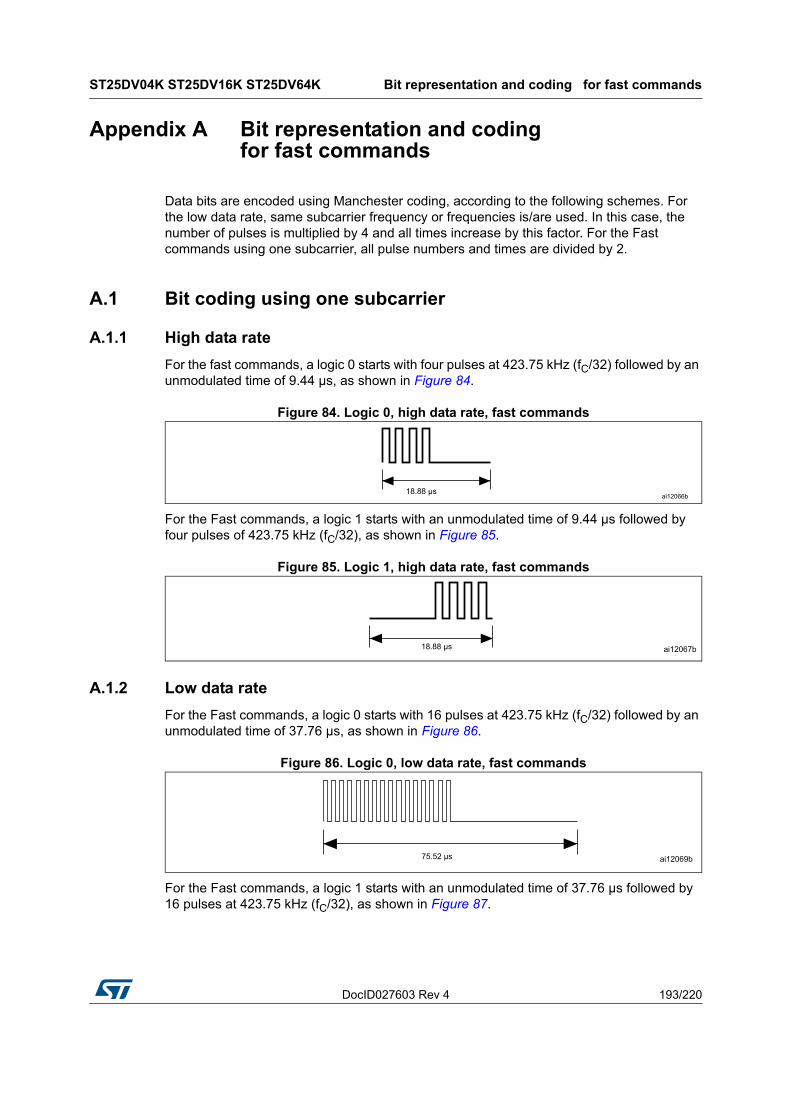
DocID027603 Rev 4 193/220
ST25DV04K ST25DV16K ST25DV64K Bit representation and coding for fast commands
219
Appendix A Bit representation and coding for fast commands
Data bits are encoded using Manchester coding, according to the following schemes. For the low data rate, same subcarrier frequency or frequencies is/are used. In this case, the number of pulses is multiplied by 4 and all times increase by this factor. For the Fast commands using one subcarrier, all pulse numbers and times are divided by 2.
A.1 Bit coding using one subcarrier
A.1.1 High data rate
For the fast commands, a logic 0 starts with four pulses at 423.75 kHz (fC/32) followed by an unmodulated time of 9.44 µs, as shown in Figure 84.
Figure 84. Logic 0, high data rate, fast commands
For the Fast commands, a logic 1 starts with an unmodulated time of 9.44 µs followed by four pulses of 423.75 kHz (fC/32), as shown in Figure 85.
Figure 85. Logic 1, high data rate, fast commands
A.1.2 Low data rate
For the Fast commands, a logic 0 starts with 16 pulses at 423.75 kHz (fC/32) followed by an unmodulated time of 37.76 µs, as shown in Figure 86.
Figure 86. Logic 0, low data rate, fast commands
For the Fast commands, a logic 1 starts with an unmodulated time of 37.76 µs followed by 16 pulses at 423.75 kHz (fC/32), as shown in Figure 87.

Bit representation and coding for fast commands ST25DV04K ST25DV16K ST25DV64K
194/220 DocID027603 Rev 4
Figure 87. Logic 1, low data rate, fast commands
Note: For fast commands, bit coding using two subcarriers is not supported.
A.2 ST25DVxxx to VCD frames
Frames are delimited by an SOF and an EOF. They are implemented using code violation. Unused options are reserved for future use. For the low data rate, the same subcarrier frequency or frequencies is/are used. In this case, the number of pulses is multiplied by 4. For the Fast commands using one subcarrier, all pulse numbers and times are divided by 2.
A.3 SOF when using one subcarrier
A.3.1 High data rate
For the Fast commands, the SOF comprises an unmodulated time of 28.32 µs, followed by 12 pulses at 423.75 kHz (fC/32), and a logic 1 that consists of an unmodulated time of 9.44 µs followed by four pulses at 423.75 kHz, as shown in Figure 88.
Figure 88. Start of frame, high data rate, one subcarrier, fast commands
A.3.2 Low data rate
For the Fast commands, the SOF comprises an unmodulated time of 113.28 µs, followed by 48 pulses at 423.75 kHz (fC/32), and a logic 1 that includes an unmodulated time of 37.76 µs followed by 16 pulses at 423.75 kHz, as shown in Figure 89.
Figure 89. Start of frame, low data rate, one subcarrier, fast commands

DocID027603 Rev 4 195/220
ST25DV04K ST25DV16K ST25DV64K Bit representation and coding for fast commands
219
A.4 EOF when using one subcarrier
A.4.1 High data rate
For the Fast commands, the EOF comprises a logic 0 that includes four pulses at 423.75 kHz and an unmodulated time of 9.44 µs, followed by 12 pulses at 423.75 kHz (fC/32) and an unmodulated time of 37.76 µs, as shown in Figure 90.
Figure 90. End of frame, high data rate, one subcarrier, fast commands
A.4.2 Low data rate
For the Fast commands, the EOF comprises a logic 0 that includes 16 pulses at 423.75 kHz and an unmodulated time of 37.76 µs, followed by 48 pulses at 423.75 kHz (fC/32) and an unmodulated time of 113.28 µs, as shown in Figure 91.
Figure 91. End of frame, low data rate, one subcarrier, fast commands
Note: For SOF and EOF in fast commands, bit coding using two subcarriers is not supported.
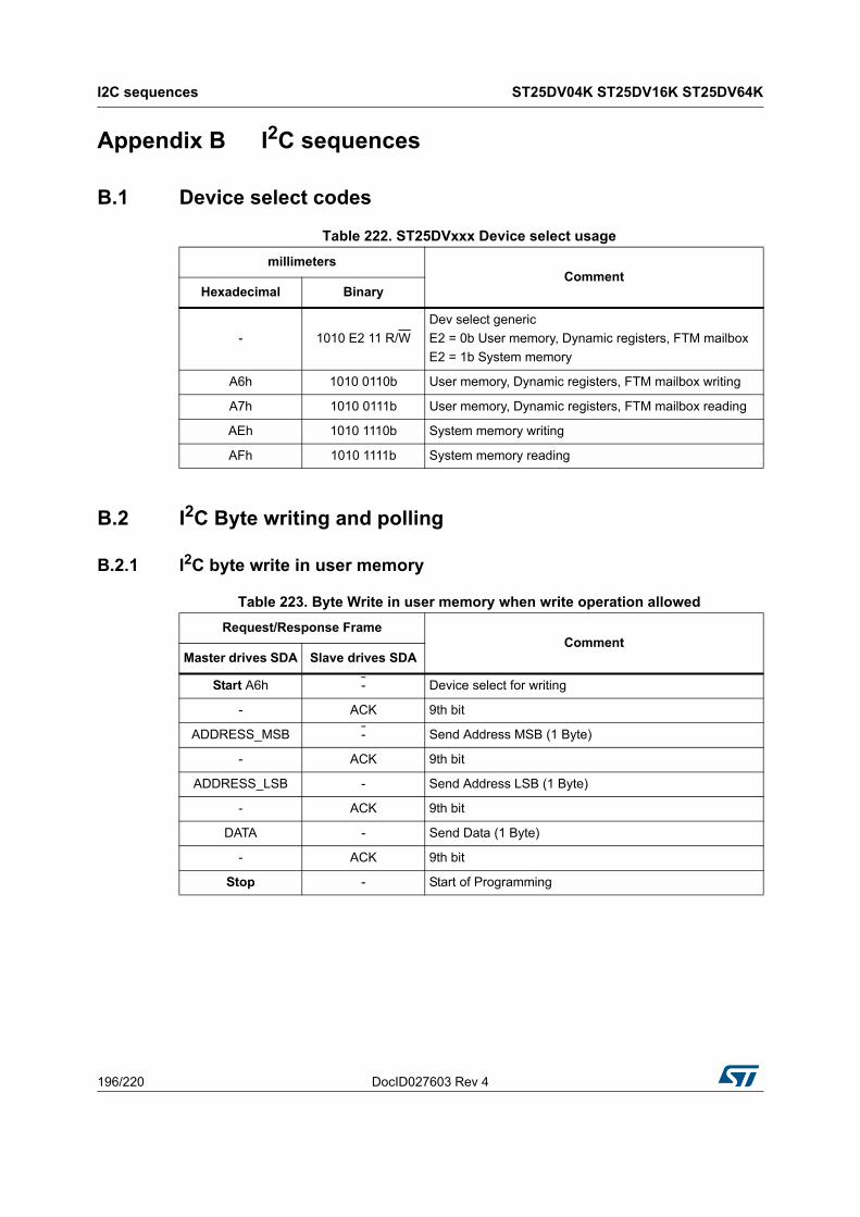
I2C sequences ST25DV04K ST25DV16K ST25DV64K
196/220 DocID027603 Rev 4
Appendix B I2C sequences
B.1 Device select codes
B.2 I2C Byte writing and polling
B.2.1 I2C byte write in user memory
Table 222. ST25DVxxx Device select usage
millimetersComment
Hexadecimal Binary
- 1010 E2 11 R/W
Dev select generic
E2 = 0b User memory, Dynamic registers, FTM mailbox
E2 = 1b System memory
A6h 1010 0110b User memory, Dynamic registers, FTM mailbox writing
A7h 1010 0111b User memory, Dynamic registers, FTM mailbox reading
AEh 1010 1110b System memory writing
AFh 1010 1111b System memory reading
Table 223. Byte Write in user memory when write operation allowed
Request/Response FrameComment
Master drives SDA Slave drives SDA
Start A6h - Device select for writing
- ACK 9th bit
ADDRESS_MSB - Send Address MSB (1 Byte)
- ACK 9th bit
ADDRESS_LSB - Send Address LSB (1 Byte)
- ACK 9th bit
DATA - Send Data (1 Byte)
- ACK 9th bit
Stop - Start of Programming

DocID027603 Rev 4 197/220
ST25DV04K ST25DV16K ST25DV64K I2C sequences
219
Table 224. Polling during programming after byte writing in user memory
Request/Response FrameComment
Master drives SDA Slave drives SDA
Start A6h - Device select for writing
- NoACK 9th bit Device Busy
Start A6h - Device select for writing
- NoACK 9th bit Device Busy
... ... Device select for writing
... ... ... 9th bit Device Busy
Start A6h - Device select for writing
- ACK9th bit Device ready
Programing completed
Stop - End of Polling
Table 225. Byte Write in user memory when write operation is not allowed
Request/Response FrameComment
Master drives SDA Slave drives SDA
Start A6h - Device select for writing
- ACK 9th bit
ADDRESS_MSB - Send Address MSB (1 Byte)
- ACK 9th bit
ADDRESS_LSB - Send Address LSB (1 Byte)
- ACK 9th bit
DATA - Send Data
- NoACK 9th bit: Write access not granted or FTM activated.
Stop -No Programming
Device return in Standby
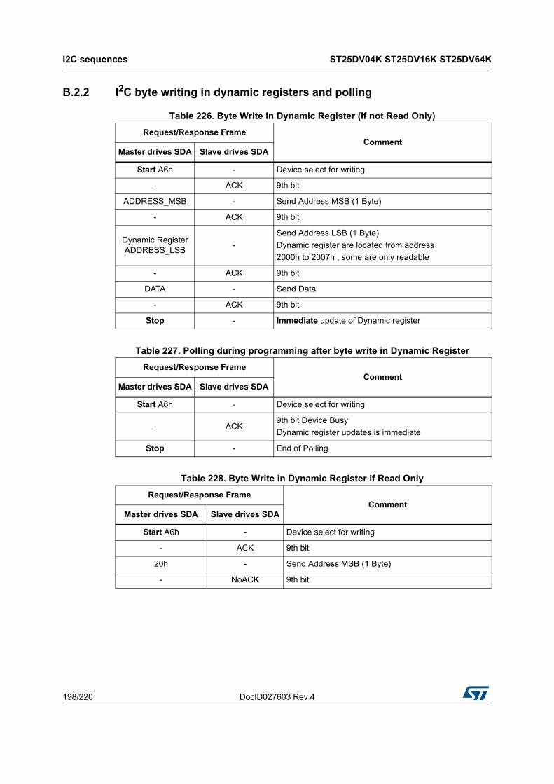
I2C sequences ST25DV04K ST25DV16K ST25DV64K
198/220 DocID027603 Rev 4
B.2.2 I2C byte writing in dynamic registers and polling
Table 226. Byte Write in Dynamic Register (if not Read Only)
Request/Response FrameComment
Master drives SDA Slave drives SDA
Start A6h - Device select for writing
- ACK 9th bit
ADDRESS_MSB - Send Address MSB (1 Byte)
- ACK 9th bit
Dynamic Register ADDRESS_LSB
-
Send Address LSB (1 Byte)
Dynamic register are located from address
2000h to 2007h , some are only readable
- ACK 9th bit
DATA - Send Data
- ACK 9th bit
Stop - Immediate update of Dynamic register
Table 227. Polling during programming after byte write in Dynamic Register
Request/Response FrameComment
Master drives SDA Slave drives SDA
Start A6h - Device select for writing
- ACK9th bit Device Busy
Dynamic register updates is immediate
Stop - End of Polling
Table 228. Byte Write in Dynamic Register if Read Only
Request/Response FrameComment
Master drives SDA Slave drives SDA
Start A6h - Device select for writing
- ACK 9th bit
20h - Send Address MSB (1 Byte)
- NoACK 9th bit
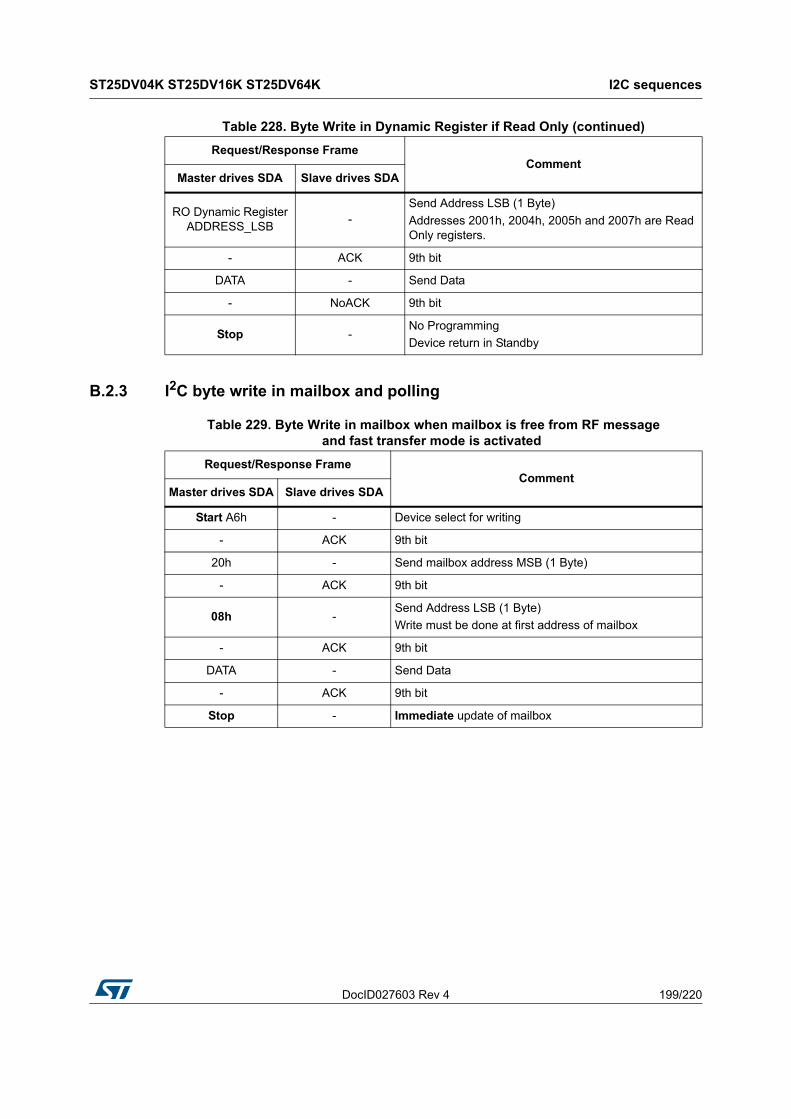
DocID027603 Rev 4 199/220
ST25DV04K ST25DV16K ST25DV64K I2C sequences
219
B.2.3 I2C byte write in mailbox and polling
RO Dynamic Register ADDRESS_LSB
-Send Address LSB (1 Byte)
Addresses 2001h, 2004h, 2005h and 2007h are Read Only registers.
- ACK 9th bit
DATA - Send Data
- NoACK 9th bit
Stop -No Programming
Device return in Standby
Table 228. Byte Write in Dynamic Register if Read Only (continued)
Request/Response FrameComment
Master drives SDA Slave drives SDA
Table 229. Byte Write in mailbox when mailbox is free from RF message and fast transfer mode is activated
Request/Response FrameComment
Master drives SDA Slave drives SDA
Start A6h - Device select for writing
- ACK 9th bit
20h - Send mailbox address MSB (1 Byte)
- ACK 9th bit
08h -Send Address LSB (1 Byte)
Write must be done at first address of mailbox
- ACK 9th bit
DATA - Send Data
- ACK 9th bit
Stop - Immediate update of mailbox

I2C sequences ST25DV04K ST25DV16K ST25DV64K
200/220 DocID027603 Rev 4
B.2.4 I2C byte write and polling in system memory
Table 230. Byte Write in mailbox when mailbox is not free from RF message fast transfer mode is not activated
Request/Response FrameComment
Master drives SDA Slave drives SDA
Start A6h - Device select for writing
- ACK 9th bit
20h - Send mailbox address MSB (1 Byte)
- ACK 9th bit
08h -Send Address LSB (1 Byte)
Write must be done at first address of mailbox
- ACK 9th bit
DATA - Send Data
- NoACK9th bit Access
Mailbox busy or FTM not activated
Stop -No Programming
Device return in Standby
Table 231. Byte Write in System memory if I2C security session is open and register is not RO
Request/Response FrameComment
Master drives SDA Slave drives SDA
Start AEh - Device select for writing
- ACK 9th bit
ADDRESS_MSB - Send Address MSB (1 Byte)
- ACK 9th bit
ADDRESS_LSB - Send Address LSB (1 Byte)
- ACK 9th bit
DATA - Send Data
- ACK 9th bit
Stop - Start of Programming

DocID027603 Rev 4 201/220
ST25DV04K ST25DV16K ST25DV64K I2C sequences
219
Table 232. Polling during programing after byte write in System memory
if I2C security session is open and register is not RO
Request/Response FrameComment
Master drives SDA Slave drives SDA
Start AEh - Device select for writing
- NoACK 9th bit Device Busy
Start AEh - Device select for writing
- NoACK 9th bit Device Busy
Start AEh - Device select for writing
- ... 9th bit
Start AEh - Device select for writing
- ACK9th bit Device ready
Programing completed
Stop - end of Polling
Table 233. Byte Write in System memory if I2C security session is closed or register is RO
Request/Response FrameComment
Master drives SDA Slave drives SDA
Start AEh - Device select for writing
- ACK 9th bit
ADDRESS_MSB - Send Address MSB (1 Byte)
- ACK 9th bit
ADDRESS_LSB - Send Address LSB (1 Byte)
- ACK 9th bit
DATA - Send Data
- NoACK 9th bit
Stop -No Programming
Device return in Standby
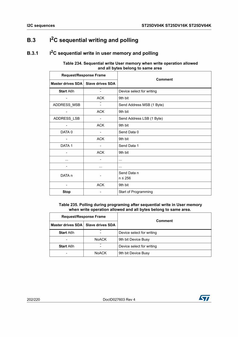
I2C sequences ST25DV04K ST25DV16K ST25DV64K
202/220 DocID027603 Rev 4
B.3 I2C sequential writing and polling
B.3.1 I2C sequential write in user memory and polling
Table 234. Sequential write User memory when write operation allowed and all bytes belong to same area
Request/Response FrameComment
Master drives SDA Slave drives SDA
Start A6h - Device select for writing
- ACK 9th bit
ADDRESS_MSB - Send Address MSB (1 Byte)
- ACK 9th bit
ADDRESS_LSB - Send Address LSB (1 Byte)
- ACK 9th bit
DATA 0 - Send Data 0
- ACK 9th bit
DATA 1 - Send Data 1
- ACK 9th bit
... - ...
- ... ...
DATA n -Send Data n
n ≤ 256
- ACK 9th bit
Stop - Start of Programming
Table 235. Polling during programing after sequential write in User memory when write operation allowed and all bytes belong to same area.
Request/Response FrameComment
Master drives SDA Slave drives SDA
Start A6h - Device select for writing
- NoACK 9th bit Device Busy
Start A6h - Device select for writing
- NoACK 9th bit Device Busy

DocID027603 Rev 4 203/220
ST25DV04K ST25DV16K ST25DV64K I2C sequences
219
Start A6h - Device select for writing
- ... 9th bit Device Busy
Start A6h - Device select for writing
- ACK9th bit Device ready
Programing completed
Stop - End of Polling
Table 236. Sequential write in User memory when write operation allowed and crossing over area border
Request/Response FrameComment
Master drives SDA Slave drives SDA
Start A6h - Device select for writing
- ACK 9th bit
ADDRESS_MSB - Send Address MSB (1 Byte)
- ACK 9th bit
ADDRESS_LSB - Send Address LSB (1 Byte)
- ACK 9th bit
DATA 0 - Send Data 0
- ACK 9th bit
DATA 1 - Send Data 1
- ACK 9th bit
... - ...
- ... ...
DATA n -Send Data n
Address is located in next memory area
- NoACK 9th bit
Stop -No programming
Device return in Standby
Table 235. Polling during programing after sequential write in User memory when write operation allowed and all bytes belong to same area. (continued)
Request/Response FrameComment
Master drives SDA Slave drives SDA

I2C sequences ST25DV04K ST25DV16K ST25DV64K
204/220 DocID027603 Rev 4
B.3.2 I2C sequential write in mailbox and polling
Table 237. Polling during programing after sequential write in User memory when write operation allowed and crossing over area border
Request/Response FrameComment
Master drives SDA Slave drives SDA
Start A6h - Device select for writing
- ACK9th bit Device ready
No programming
Stop - End of Polling
Table 238. Sequential write in mailbox when mailbox is free from RF message and fast transfer mode is activated
Request/Response FrameComment
Master drives SDA Slave drives SDA
Start A6h - Device select for writing
- ACK 9th bit
ADDRESS_MSB - Send mailbox Address MSB (1 Byte)
- ACK 9th bit
ADDRESS_LSB - Send mailbox Address LSB (1 Byte)
- ACK 9th bit
DATA 0 - Send Data 0
- ACK 9th bit
DATA 1 - Send Data 1
- ACK 9th bit
... - ...
- ... ...
DATA n -Send Data n
n ≤ 256
- ACK 9th bit
Stop - Immediate mailbox content update
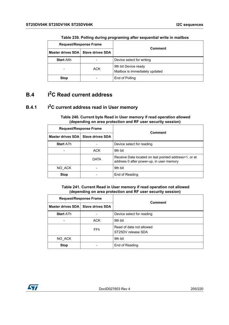
DocID027603 Rev 4 205/220
ST25DV04K ST25DV16K ST25DV64K I2C sequences
219
B.4 I2C Read current address
B.4.1 I2C current address read in User memory
Table 239. Polling during programing after sequential write in mailbox
Request/Response FrameComment
Master drives SDA Slave drives SDA
Start A6h - Device select for writing
- ACK9th bit Device ready
Mailbox is immediately updated
Stop - End of Polling
Table 240. Current byte Read in User memory if read operation allowed (depending on area protection and RF user security session)
Request/Response FrameComment
Master drives SDA Slave drives SDA
Start A7h - Device select for reading
- ACK 9th bit
DATAReceive Data located on last pointed address+1, or at address 0 after power-up, in user memory
NO_ACK - 9th bit
Stop - End of Reading
Table 241. Current Read in User memory if read operation not allowed (depending on area protection and RF user security session)
Request/Response FrameComment
Master drives SDA Slave drives SDA
Start A7h - Device select for reading
- ACK 9th bit
FFhRead of data not allowed
ST25DV release SDA
NO_ACK 9th bit
Stop - End of Reading

I2C sequences ST25DV04K ST25DV16K ST25DV64K
206/220 DocID027603 Rev 4
B.5 I2C random address read
B.5.1 I2C random address read in user memory
Table 242. Random byte read in User memory if read operation allowed (depending on area protection and RF user security session)
Request/Response FrameComment
Master drives SDA Slave drives SDA
Start A6h - Device select for writing
- ACK 9th bit
ADDRESS_MSB - Send Address MSB (1 Byte)
- ACK 9th bit
ADDRESS_LSB - Send Address LSB (1 Byte)
- ACK 9th bit
Start A7h - Device select for reading
- ACK 9th bit
- DATA Receive Data
NO_ACK - 9th bit
Stop - End of Reading
Table 243. Random byte read in User memory if operation not allowed (depending on area protection and RF user security)
Request/Response FrameComment
Master drives SDA Slave drives SDA
Start A6h - Device select for writing
- ACK 9th bit
ADDRESS_MSB - Send Address MSB (1 Byte)
- ACK 9th bit
ADDRESS_LSB - Send Address LSB (1 Byte)
- ACK 9th bit
Start A7h - Device select for reading
- ACK 9th bit
- FFhRead of data not allowed
ST25DVxxx release SDA
NO_ACK - 9th bit
Stop - End of Reading

DocID027603 Rev 4 207/220
ST25DV04K ST25DV16K ST25DV64K I2C sequences
219
B.5.2 I2C Random address read in system memory
B.5.3 I2C Random address read in dynamic registers
Table 244. Byte Read System memory (Static register or I2C Password after a valid Present I2C Password)
Request/Response FrameComment
Master drives SDA Slave drives SDA
Start AEh - Device select for writing
- ACK 9th bit
ADDRESS_MSB - Send Address MSB (1 Byte)
- ACK 9th bit
ADDRESS_LSB - Send Address LSB (1 Byte)
- ACK 9th bit
Start AFh - Device select for reading
- ACK 9th bit
- DATA Receive Data
NO_ACK - 9th bit
Stop - End of reading
Table 245. Random byte read in Dynamic registers
Request/Response FrameComment
Master drives SDA Slave drives SDA
Start A6h - Device select for writing
- ACK 9th bit
20h - Send Address MSB (1 Byte)
- ACK 9th bit
ADDRESS_LSB - Send Adress LSB (1 Byte)
- ACK 9th bit
Start A7h - Device select for reading
- ACK 9th bit
- DATA Receive Data
NO_ACK - 9th bit
Stop - End of reading

I2C sequences ST25DV04K ST25DV16K ST25DV64K
208/220 DocID027603 Rev 4
B.6 I2C sequential read
B.6.1 I2C sequential read in user memory
Table 246. Sequential Read User memory if read operation allowed (depending on area protection and RF user security session)
and all bytes belong to the same area
Request/Response FrameComment
Master drives SDA Slave drives SDA
Start A6h - Device select for writing
- ACK 9th bit
ADDRESS_MSB - Send Address MSB (1 Byte)
- ACK 9th bit
ADDRESS_LSB - Send Address LSB (1 Byte)
- ACK 9th bit
Start A7h0 - Device select for reading
- ACK 9th bit
- DATA 0 Receive Data 0
ACK - 9th bit
- DATA 1 Receive Data 1
ACK - 9th bit
- ... ...
... - ...
- DATA n Receive Data n
NO_ACK - 9th bit
Stop - End of Reading
Table 247. Sequential Read User memory if read operation allowed (depending on area protection and RF user security session)
but crossing area border
Request/Response FrameComment
Master drives SDA Slave drives SDA
Start A6h - Device select for writing
- ACK 9th bit
ADDRESS_MSB - Send Address MSB (1 Byte)
- ACK 9th bit
ADDRESS_LSB - Send Address LSB (1 Byte)
- ACK 9th bit

DocID027603 Rev 4 209/220
ST25DV04K ST25DV16K ST25DV64K I2C sequences
219
Start A7h - Device select for reading
- ACK 9th bit
- DATA 0 Receive Data 0
ACK - 9th bit
- DATA 1 Receive Data 1
ACK - 9th bit
- ... ...
... - ...
- DATA n Receive Data last Address available
ACK - 9th bit
- FFhData is located in next memory area
ST25DV release SDA
ACK - 9th bit
- ... ...
... - ...
- FFhData is located in next memory area
ST25DV release SDA
Stop - End of reading
Table 248. Sequential Read User memory if read operation allowed (depending on area protection and RF user security session)
Request/Response FrameComment
Master drives SDA Slave drives SDA
Start A6h - Device select for writing
- ACK 9th bit
ADDRESS_MSB - Send Address MSB (1 Byte)
- ACK 9th bit
ADDRESS_LSB - Send Address LSB (1 Byte)
- ACK 9th bit
Start A7h - Device select for reading
- ACK 9th bit
- FFhST25DV release SDA
Reading access not granted
Table 247. Sequential Read User memory if read operation allowed (depending on area protection and RF user security session)
but crossing area border (continued)
Request/Response FrameComment
Master drives SDA Slave drives SDA

I2C sequences ST25DV04K ST25DV16K ST25DV64K
210/220 DocID027603 Rev 4
B.6.2 I2C sequential read in system memory
ACK - 9th bit
- ... ...
... - ...
- FFhST25DV release SDA
Reading access not granted
NO_ACK - 9th bit
Stop - End of reading
Table 248. Sequential Read User memory if read operation allowed (depending on area protection and RF user security session) (continued)
Request/Response FrameComment
Master drives SDA Slave drives SDA
Table 249. Sequential in Read System memory (I2C security session open if reading I2C_PWD)
Request/Response FrameComment
Master drives SDA Slave drives SDA
Start AEh - Device select for writing
- ACK 9th bit
ADDRESS_MSB - Send Address MSB (1 Byte)
- ACK 9th bit
ADDRESS_LSB - Send Address LSB (1 Byte)
- ACK 9th bit
Start AF7h - Device select for reading
- ACK 9th bit
- DATA Receive Data 0
ACK - 9th bit
- DATA Receive Data 1
ACK - 9th bit
- ... ...
... - ...
- DATA Receive Data n
NO_ACK - 9th bit
Stop - End of Reading

DocID027603 Rev 4 211/220
ST25DV04K ST25DV16K ST25DV64K I2C sequences
219
B.6.3 I2C sequential read in dynamic registers
Table 250. Sequential Read system memory when access is not granted
(I2C password I2C_PWD)
Request/Response FrameComment
Master drives SDA Slave drives SDA
Start AEh - Device select for writing
- ACK 9th bit
90h - Send Address MSB (1 Byte)
- ACK 9th bit
ADDRESS_LSB - Send Address LSB (1 Byte)
- ACK 9th bit
Start AFh - Device select for reading
- ACK 9th bit
- DATA Receive Data 0
- FFhST25DV release SDA
Reading access is not granted
ACK - 9th bit
- ... ...
... - ...
- FFhST25DV release SDA
Reading access is not granted
NO_ACK - 9th bit
Stop - End of reading
Table 251. Sequential read in dynamic register
Request/Response FrameComment
Master drives SDA Slave drives SDA
Start A6h - Device select for writing
- ACK 9th bit
20h - Send Address MSB (1 Byte)
- ACK 9th bit
Dynamic register ADDRESS_LSB
-Send Address LSB (1 Byte)
Fynamic register are located form address 2000h to 2007
- ACK 9th bit
Start A7h - Device select for reading
- ACK 9th bit

I2C sequences ST25DV04K ST25DV16K ST25DV64K
212/220 DocID027603 Rev 4
- DATA Receive Data 0
ACK - 9th bit
- DATA Receive Data 1
ACK - 9th bit
- ... ...
... - ...
- Data Receive Data n
NO_ACK - 9th bit
Stop - End of reading
Table 252. Sequential read in Dynamic register and mailbox continuously if fast transfer mode is activated
Request/Response FrameComment
Master drives SDA Slave drives SDA
Start A6h - Device select for writing
- ACK 9th bit
20h - Send Address MSB (1 Byte)
- ACK 9th bit
Dynamic RegisterADDRESS_LSB
-
Send Address LSB (1 Byte)
Dynamic register are located from address
2000h to 2007h
- ACK 9th bit
Start A7h - Device select for reading
- ACK 9th bit
- DATA 0 Receive Data 0
ACK - 9th bit
- DATA 1 Receive Data 1
ACK - 9th bit
- ... ...
... - ...
- DATA nReceive Data n (n ≤ 8)
Last Dynamic register address 2007h
ACK - 9th bit
- DATA n + 1 Mailbox byte 0
Table 251. Sequential read in dynamic register (continued)
Request/Response FrameComment
Master drives SDA Slave drives SDA
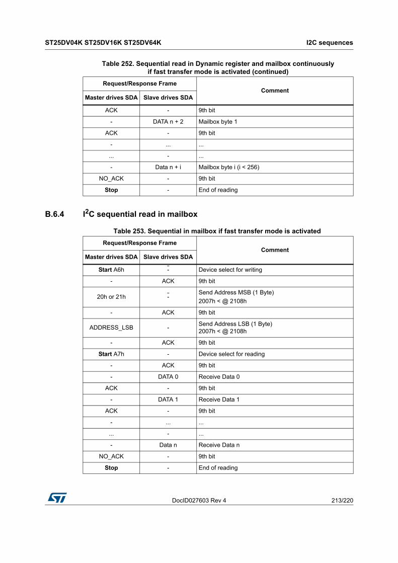
DocID027603 Rev 4 213/220
ST25DV04K ST25DV16K ST25DV64K I2C sequences
219
B.6.4 I2C sequential read in mailbox
ACK - 9th bit
- DATA n + 2 Mailbox byte 1
ACK - 9th bit
- ... ...
... - ...
- Data n + i Mailbox byte i (i < 256)
NO_ACK - 9th bit
Stop - End of reading
Table 252. Sequential read in Dynamic register and mailbox continuously if fast transfer mode is activated (continued)
Request/Response FrameComment
Master drives SDA Slave drives SDA
Table 253. Sequential in mailbox if fast transfer mode is activated
Request/Response FrameComment
Master drives SDA Slave drives SDA
Start A6h - Device select for writing
- ACK 9th bit
20h or 21h -Send Address MSB (1 Byte)
2007h < @ 2108h
- ACK 9th bit
ADDRESS_LSB -Send Address LSB (1 Byte) 2007h < @ 2108h
- ACK 9th bit
Start A7h - Device select for reading
- ACK 9th bit
- DATA 0 Receive Data 0
ACK - 9th bit
- DATA 1 Receive Data 1
ACK - 9th bit
- ... ...
... - ...
- Data n Receive Data n
NO_ACK - 9th bit
Stop - End of reading

I2C sequences ST25DV04K ST25DV16K ST25DV64K
214/220 DocID027603 Rev 4
Table 254. Sequential read in mailbox if fast transfer mode is not activated
Request/Response FrameComment
Master drives SDA Slave drives SDA
Start A6h - Device select for writing
- ACK 9th bit
20h or 21h -Send Address MSB (1 Byte)
2007h < @ 2108h
- ACK 9th bit
ADDRESS_LSB -Send Address LSB (1 Byte) 2007h < @ 2108h
- ACK 9th bit
Start A7h - Device select for reading
- ACK 9th bit
- FFh ST25DVxxx release SDA
ACK - 9th bit
- FFh ST25DVxxx release SDA
ACK - 9th bit
- ... ...
... - ...
- FFh ST25DVxxx release SDA
NO_ACK - 9th bit
Stop - End of reading

DocID027603 Rev 4 215/220
ST25DV04K ST25DV16K ST25DV64K I2C sequences
219
B.7 I2C password relative sequences
B.7.1 I2C write password
Table 255. Write Password when I2C security session is already open and fast transfer mode is not activated
Request/Response FrameComment
Master drives SDA Slave drives SDA
Start AEh - Device select for writing
- ACK 9th bit
09h - Send I2C_PWD MSB address
- ACK 9th bit
00h - Send I2C_PWD LSB address
- ACK 9th bit
I2C_PWD_BYTE_7 - Send I2C_PWD MSB
- ACK 9th bit
I2C_PWD_BYTE_6 DATA 0 Send Data
- ACK 9th bit
... - ...
- ... ...
I2C_PWD_BYTE_0 - Send I2C_PWD LSB
- ACK 9th bit
07h - Write password command
- ACK 9th bit
I2C_PWD_BYTE_7 - Send I2C_PWD MSB
- ACK 9th bit
I2C_PWD_BYTE_6 DATA 0 Send Data
- ACK 9th bit
... - ...
- ... ...
I2C_PWD_BYTE_0 - Send I2C_PWD LSB
- ACK 9th bit
Stop - Start of I2C password programming

I2C sequences ST25DV04K ST25DV16K ST25DV64K
216/220 DocID027603 Rev 4
B.7.2 I2C present password
Table 256. Write Password when I2C security session is not open or fast transfer mode activated
Request/Response FrameComment
Master drives SDA Slave drives SDA
Start AEh - Device select for writing
- ACK 9th bit
09h - Send I2C_PWD MSB address
- ACK 9th bit
00h - Send I2C_PWD LSB address
- NoACK 9th bit
Stop -No PWD Programming
Device return in Standby
Present Password (whatever status of I2C security session or fast transfer mode)
Request/Response FrameComment
Master drives SDA Slave drives SDA
Start AEh - Device select for writing
- ACK 9th bit
09h - Send I2C_PWD MSB address
- ACK 9th bit
00h - Send I2C_PWD LSB address
- ACK 9th bit
I2C_PWD_BYTE_7 - Send I2C_PWD MSB
- ACK 9th bit
I2C_PWD_BYTE_6 DATA 0 Send Data
- ACK 9th bit
... - ...
- ... ...
I2C_PWD_BYTE_0 - Send I2C_PWD LSB
- ACK 9th bit
09h - Present password command
- ACK 9th bit
I2C_PWD_BYTE_7 - Send I2C_PWD MSB
- ACK 9th bit
I2C_PWD_BYTE_6 - Send Data

DocID027603 Rev 4 217/220
ST25DV04K ST25DV16K ST25DV64K I2C sequences
219
- ACK 9th bit
... - ...
- ... ...
I2C_PWD_BYTE_0 - Send I2C_PWD LSB
- ACK 9th bit
Stop -ST25DV with active I2C_PWD.
Result is immediate.
Present Password (whatever status of I2C security session or fast transfer mode)
Request/Response FrameComment
Master drives SDA Slave drives SDA
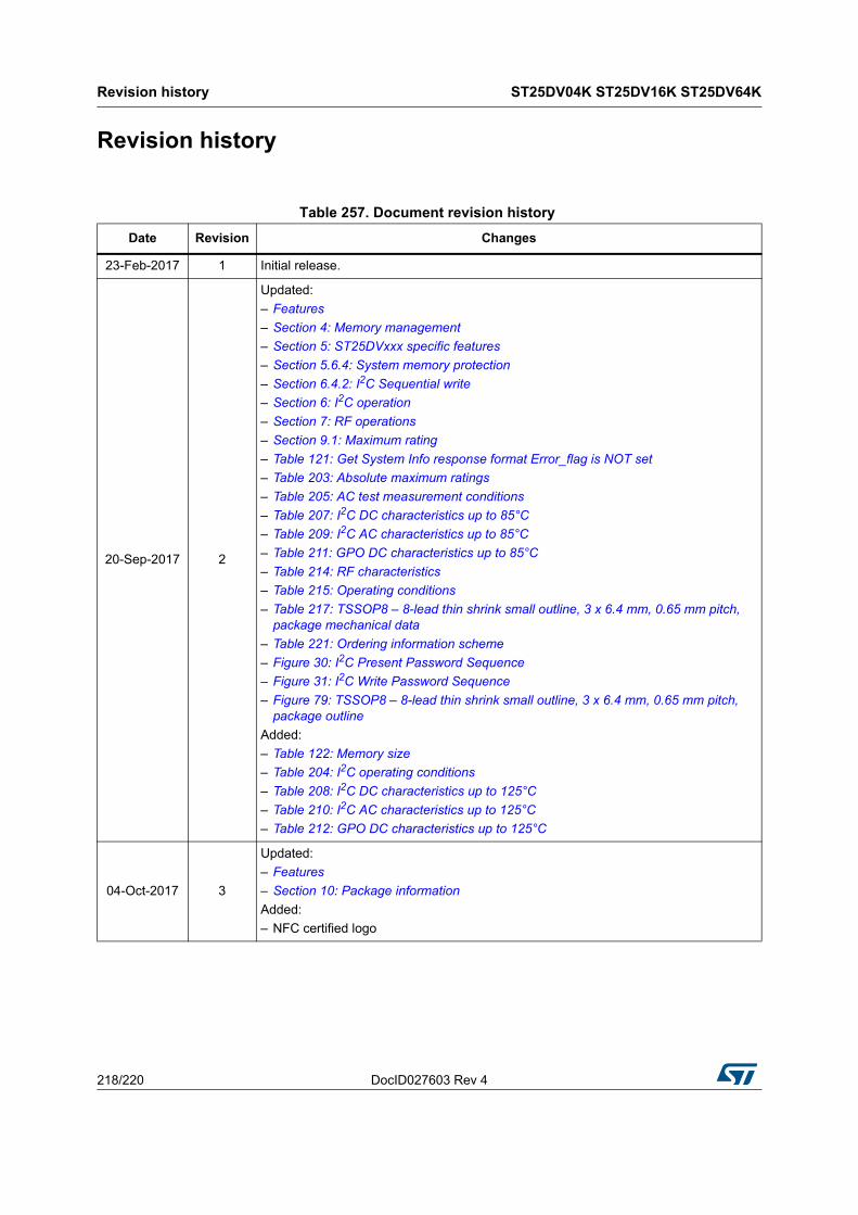
Revision history ST25DV04K ST25DV16K ST25DV64K
218/220 DocID027603 Rev 4
Revision history
Table 257. Document revision history
Date Revision Changes
23-Feb-2017 1 Initial release.
20-Sep-2017 2
Updated:
– Features
– Section 4: Memory management
– Section 5: ST25DVxxx specific features
– Section 5.6.4: System memory protection
– Section 6.4.2: I2C Sequential write
– Section 6: I2C operation
– Section 7: RF operations
– Section 9.1: Maximum rating
– Table 121: Get System Info response format Error_flag is NOT set
– Table 203: Absolute maximum ratings
– Table 205: AC test measurement conditions
– Table 207: I2C DC characteristics up to 85°C
– Table 209: I2C AC characteristics up to 85°C
– Table 211: GPO DC characteristics up to 85°C
– Table 214: RF characteristics
– Table 215: Operating conditions
– Table 217: TSSOP8 – 8-lead thin shrink small outline, 3 x 6.4 mm, 0.65 mm pitch, package mechanical data
– Table 221: Ordering information scheme
– Figure 30: I2C Present Password Sequence
– Figure 31: I2C Write Password Sequence
– Figure 79: TSSOP8 – 8-lead thin shrink small outline, 3 x 6.4 mm, 0.65 mm pitch, package outline
Added:
– Table 122: Memory size
– Table 204: I2C operating conditions
– Table 208: I2C DC characteristics up to 125°C
– Table 210: I2C AC characteristics up to 125°C
– Table 212: GPO DC characteristics up to 125°C
04-Oct-2017 3
Updated:
– Features
– Section 10: Package information
Added:
– NFC certified logo

DocID027603 Rev 4 219/220
ST25DV04K ST25DV16K ST25DV64K Revision history
219
19-Dec-2017 4
Added:
– Figure 4: ST25DVxxx 10-ball WLCSP package connections with Cmos interrupt output (GPO)
– Section 10.5: WLCSP10 package information
– Table 220: WLCSP - 10 balls, 1.649x1.483 mm, 0.4 mm pitch, wafer level chip scale mechanical data
– Figure 82: WLCSP - 10 balls, 1.649x1.483 mm, 0.4 mm pitch, wafer level chip scale package outline
– Figure 83: WLCSP - 10 balls, 1.649x1.483 mm, 0.4 mm pitch, wafer level chip scale recommended footprint
Updated:
– Features
– Section 1: Description
– Section 2.5: Energy harvesting analog output (V_EH)
– Section 5.3.2: Energy harvesting feature description
– Figure 21: ST25DVxxx, Arbitration between RF and I2C
– Section 6.4.1: I2C Byte write
– Section 6.4.2: I2C Sequential write
– Table 203: Absolute maximum ratings
– Table 204: I2C operating conditions
– Table 221: Ordering information scheme
Deleted:
– Device summary
Table 257. Document revision history (continued)
Date Revision Changes
ST25DV04K ST25DV16K ST25DV64K
220/220 DocID027603 Rev 4
3
IMPORTANT NOTICE – PLEASE READ CAREFULLY
STMicroelectronics NV and its subsidiaries (“ST”) reserve the right to make changes, corrections, enhancements, modifications, and improvements to ST products and/or to this document at any time without notice. Purchasers should obtain the latest relevant information on ST products before placing orders. ST products are sold pursuant to ST’s terms and conditions of sale in place at the time of order acknowledgement.
Purchasers are solely responsible for the choice, selection, and use of ST products and ST assumes no liability for application assistance or the design of Purchasers’ products.
No license, express or implied, to any intellectual property right is granted by ST herein.
Resale of ST products with provisions different from the information set forth herein shall void any warranty granted by ST for such product.
ST and the ST logo are trademarks of ST. All other product or service names are the property of their respective owners.
Information in this document supersedes and replaces information previously supplied in any prior versions of this document.
© 2017 STMicroelectronics – All rights reserved