e-beam lithography on transparent substrates: challenges
TRANSCRIPT

Vistec Electron Beam • www.vistec-semi.com
Vistec Electron Beam
E-beam lithography on transparent
substrates: challenges and
results
Thomas Händel

Vistec Electron Beam
Outline
• Motivation
• Material properties
• Experimental samples, process and electron-beam lithography system
• Experimental steps and results
• Conclusion
• Acknowledgement
27.10.2011 Beams & More 2011 page 2

Vistec Electron Beam
Motivation
Suppliers view
• Large variety of transparent substrates for the semiconductor industry
• Among them are Quartz, Boron Nitride (BN), Gallium Nitride (GaN), Sapphire
(Crystal of Al2O3), Silicon Carbide (SiC) and others
• Check and ensure the functionality of the electron-beam lithography system from the
automatic handling until the exposure of the substrates
• Requests from potential and existing customers
27.10.2011 Beams & More 2011 page 3

Vistec Electron Beam
Motivation
Customers view
• GaN material of choice for applications in high-power and high-frequency as well as
optoelectronic devices
• Increased product development in the commercial market such as wireless
infrastructure, cable television, satellite and power electronics*
• Development of high-performance GaN-on-SiC power transistors at NXP
Semiconductors**
– Excellent thermal properties of SiC Higher operating temperatures
– High electron drift velocity and large electrical field breakdown of GaN
Increase in extended frequency range, efficiency and power density performance
• Development of High Brightness Light-Emitting Diodes (HB LED’s) at Optogan**
– Large band gap and stimulated emission at room-temperature Enhanced
power efficiency and highest light intensity
* Source: CS Europe, Frankfurt/Main, March 2011, ** Source: Compound Semiconductor Magazine, August/September 2011
27.10.2011 Beams & More 2011 page 4

Vistec Electron Beam
Outline
• Motivation
• Material properties
• Experimental samples, process and electron-beam lithography system
• Experimental steps and results
• Conclusion
• Acknowledgement
27.10.2011 Beams & More 2011 page 5

Vistec Electron Beam
Material properties
27.10.2011 Beams & More 2011 page 6
Si GaAs GaN SiC
Density1, g/cm3 2.33 5.32 6.15 3.16…3.21
Dielectric constant1 11.7 12.9..13.1 8.9…9.7 9.66…10.03
Refractive index1, 2 3.42
Opaque
3.3..3.6
Opaque
2.3…2.4
Transparent
2.55…2.59
Transparent
Linear thermal expansion, 10-6 1/K 2.6 5.73..5.8 3.1…5.9 2.77
Resistivity1, cm up to 105 up to 108 up to 1010 up to 1010
Thermal conductivity1, W/cmK 1.31 0.46..0.55 1.3 3.6..4.9
Young’s module1, GPa 62…202 86 105…398 52...553
Current wafer size, mm up to 450 up to 150 up to 100 up to 100 1 at 300K 2 infrared refractive index
- Values vary depending on modification and source
Vistec Electron Beam
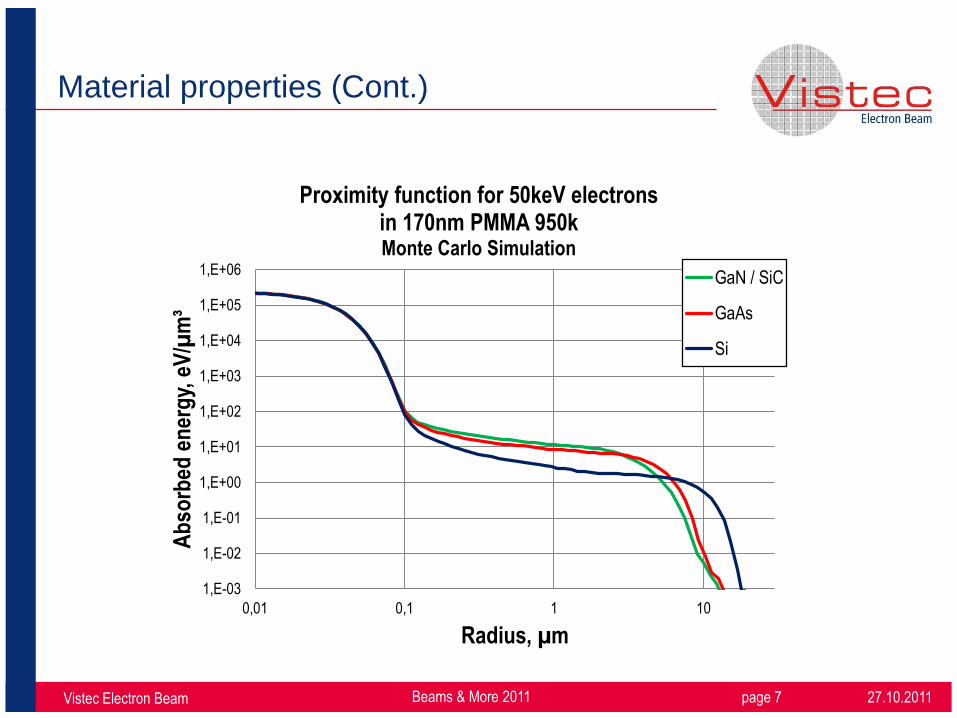
Material properties (Cont.)
27.10.2011 Beams & More 2011 page 7
1,E-03
1,E-02
1,E-01
1,E+00
1,E+01
1,E+02
1,E+03
1,E+04
1,E+05
1,E+06
0,01 0,1 1 10
Ab
sorb
ed e
ner
gy,
eV
/µm
³
Radius, µm
Proximity function for 50keV electrons in 170nm PMMA 950k Monte Carlo Simulation
GaN / SiC
GaAs
Si

Vistec Electron Beam
Material properties (Cont.)
• Back scattering on GaAs and GaN larger than on Si substrates Individual
proximity correction function required for each substrate material
• Adaption of proximity correction is a default procedure in electron-beam
lithography No special requirements on transparent substrates
27.10.2011 Beams & More 2011 page 8

Vistec Electron Beam
Outline
• Motivation
• Material properties
• Experimental samples, process and electron-beam lithography system
• Experimental steps and results
• Conclusion
• Acknowledgement
27.10.2011 Beams & More 2011 page 9

Vistec Electron Beam
Experimental samples
Substrate number Material Diameter, mm Total thickness, mm
#1 GaN on SiC 50 325
#2 GaN on SiC 76 365
#3 GaN on SiC 76 350
#4 SiC 100 400
27.10.2011 Beams & More 2011 page 10
GaN
SiC
2mm
363mm
Substrate #2
SiC
400mm
Substrate #4

Vistec Electron Beam
Process
Process steps
1. Coating: 170nm PMMA 950k, 180°C, 3min
2. Au evaporation (Anti-charging layer)
3. Exposure
4. Au removal
5. Development: MIBK:IPA=1:1
6. Rinse: IPA
27.10.2011 Beams & More 2011 page 11
GaN
SiC
2mm
363mm
Substrate #2
PMMA 950k
Au
170nm
20nm
SiC
400mm
Substrate #4
PMMA 950k
Au
170nm
20nm

Vistec Electron Beam
Vistec SB250 Series
27.10.2011 Beams & More 2011 page 12
Cost-effective system for mask and wafer
direct writing
Electron beam shape VSB
Acceleration voltage 50kV
Current density up to 20A/cm²
Maximum substrate size
wafers up to 200mm
masks up to 7 inch
Stage travel range 210 x 210mm²
Laser interferometer / 1024
Minimum feature size < 50nm
25nm (HSQ)
Source: Ferdinand-Braun-Institut für Höchstfrequenztechnik,
Berlin, Germany

Vistec Electron Beam
Outline
• Motivation
• Material properties
• Experimental samples, process and electron-beam lithography system
• Experimental steps and results
• Conclusion
• Acknowledgement
27.10.2011 Beams & More 2011 page 13

Vistec Electron Beam
Experimental steps
1. Check and ensure the functionality of
a. Sensors to be used for substrate recognition and tracking
b. Prealigner to be used for substrate alignment
c. Fully automatic substrate handling
d. Electrostatic chuck and height measurement
e. Process
f. Exposure
2. Inspection and measurement
27.10.2011 Beams & More 2011 page 14

Vistec Electron Beam
Substrate alignment
Fully automated prealignment
Alignment results
• Alignment offset ≤ 10µm
• Alignment angle ≤ 0.4mrad
27.10.2011 Beams & More 2011 page 15
1200
1250
1300
1350
1400
1450
1500
1550
1600
125
150
175
110
0112
5115
0117
5120
0122
5125
0127
5130
0132
5135
0137
5140
0142
5145
0147
5150
0152
5155
0157
51
Encoder counts
CC
D s
igna
l
Main flat
Second flat

Vistec Electron Beam
Fully automated Shaped Beam Systems
27.10.2011 Beams & More 2011 page 16
Cassette-to-cassette
Material handling
for mask and wafer
substrates
Example: SB250 Series – 200mm platform
Vistec Electron Beam
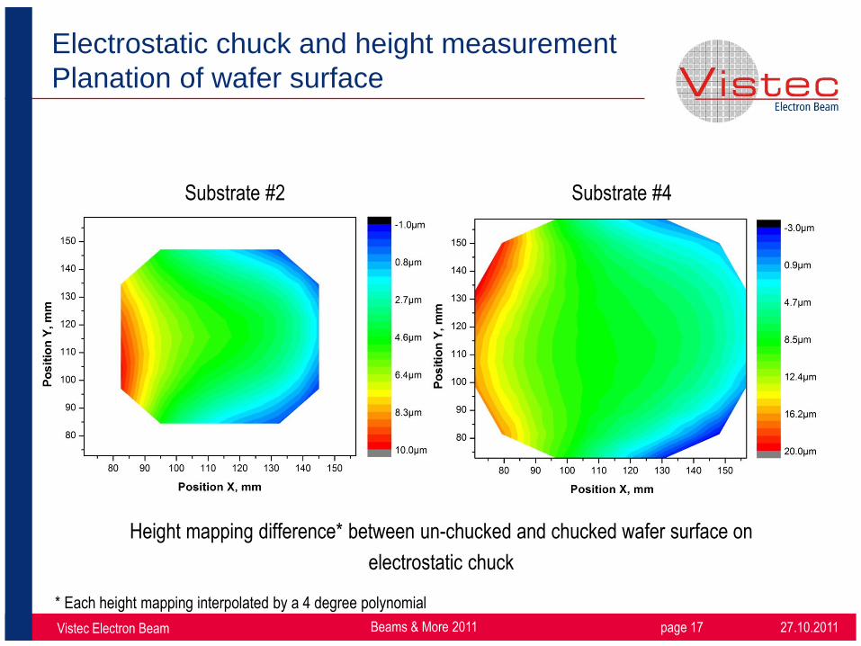
Electrostatic chuck and height measurement
Planation of wafer surface
Height mapping difference* between un-chucked and chucked wafer surface on
electrostatic chuck
* Each height mapping interpolated by a 4 degree polynomial
27.10.2011 Beams & More 2011 page 17
Substrate #2 Substrate #4

Vistec Electron Beam
Exposure results
Core and pad of gates
100nm core in 170nm PMMA 950k
27.10.2011 Beams & More 2011 page 18
Substrate #2
101nm 101nm

Vistec Electron Beam
Exposure results
Direct Write Overlay Accuracy
Pattern for first exposure run
• Cross
• Cross width 1.4mm
• Cross length 24mm
• Cross step 27mm
Pattern for second exposure run
• Four Angles
• Width 1.4mm
• Distance to cross 2.6mm
• No alignment marks used during exposure
27.10.2011 Beams & More 2011 page 19

Vistec Electron Beam
Exposure results
Direct Write Overlay Accuracy
Substrate #4
27.10.2011 Beams & More 2011 page 20
17nm 18nm
No alignment marks used during exposure

Vistec Electron Beam
Exposure results
Direct Write Overlay Accuracy
27.10.2011 Beams & More 2011 page 21
76mm GaAs Wafer
15nm 13nm
No alignment marks used during exposure

Vistec Electron Beam
Exposure results
Contact holes
27.10.2011 Beams & More 2011 page 22
100nm contact holes in 170nm PMMA 950k
Substrate #2
102nm

Vistec Electron Beam
Exposure results
Resolution
27.10.2011 Beams & More 2011 page 23
Lines 50nm half pitch in 170nm PMMA 950k
Substrate #2

Vistec Electron Beam
Outline
• Motivation
• Material properties
• Experimental samples, process and electron-beam lithography system
• Experimental steps and results
• Conclusion
• Acknowledgement
27.10.2011 Beams & More 2011 page 24

Vistec Electron Beam
Conclusion
• We demonstrated successfully the functionality for Vistec Shaped Beam Systems on
transparent substrates
– Sensor adjustment for recognition of opaque and transparent materials
– Fully automated handling including substrate alignment
– Electrostatic chucking and height measurement
– Exposure performance in the same range as on GaAs substrates
27.10.2011 Beams & More 2011 page 25

Vistec Electron Beam
Acknowledgement
This presentation had never been done without the cooperation and support of my
colleagues at Vistec Electron Beam GmbH.
Special thanks to Monika Böttcher, Dr. Helder Alves and Thomas Keil
27.10.2011 Beams & More 2011 page 26

Vistec Electron Beam
Thank you for your attention!
27.10.2011 Beams & More 2011 page 27