e ect of mesostructured layer upon crystalline …¬€ect of mesostructured layer upon crystalline...
TRANSCRIPT
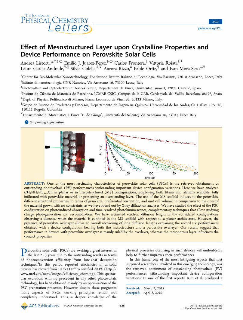
Effect of Mesostructured Layer upon Crystalline Properties andDevice Performance on Perovskite Solar CellsAndrea Listorti,*,†,‡,○ Emilio J. Juarez-Perez,§,○ Carlos Frontera,∥ Vittoria Roiati,†,⊥
Laura Garcia-Andrade,§,¶ Silvia Colella,‡,∇ Aurora Rizzo,‡ Pablo Ortiz,¶ and Ivan Mora-Sero*,§
†Center for Bio-Molecular Nanotechnology, Fondazione Istituto Italiano di Tecnologia, Via Barsanti, 73010 Arnesano, Lecce, Italy‡Istituto di nanotecnologia CNR Nanotec, Via Arnesano 16, 73100 Lecce, Italy§Photovoltaic and Optoelectronic Devices Group, Departament de Física, Universitat Jaume I, 12071 Castello, Spain∥Institut de Ciencia de Materials de Barcelona, ICMAB-CSIC, Campus de la UAB, Cerdanyola del Valles, Barcelona 08193, Spain⊥Dept. of Physics, Politecnico di Milano, Piazza Leonardo da Vinci 32, 20133 Milano, Italy¶Grupo de Diseno de Productos y Procesos, Departamento de Ingeniería Química, Universidad de los Andes, Cr 1 aEste 19A−40,110111 Bogota, Colombia∇Dipartimento di Matematica e Fisica “E. de Giorgi”, Universita del Salento, Via Arnesano 16, 73100, Lecce Italy
*S Supporting Information
ABSTRACT: One of the most fascinating characteristics of perovskite solar cells (PSCs) is the retrieved obtainment ofoutstanding photovoltaic (PV) performances withstanding important device configuration variations. Here we have analyzedCH3NH3PbI3−xClx in planar or in mesostructured (MS) configurations, employing both titania and alumina scaffolds, fullyinfiltrated with perovskite material or presenting an overstanding layer. The use of the MS scaffold induces to the perovskitedifferent structural properties, in terms of grain size, preferential orientation, and unit cell volume, in comparison to the ones ofthe material grown with no constraints, as we have found out by X-ray diffraction analyses. We have studied the effect of the PSCconfiguration on photoinduced absorption and time-resolved photoluminescence, complementary techniques that allow studyingcharge photogeneration and recombination. We have estimated electron diffusion length in the considered configurationsobserving a decrease when the material is confined in the MS scaffold with respect to a planar architecture. However, thepresence of perovskite overlayer allows an overall recovering of long diffusion lengths explaining the record PV performancesobtained with a device configuration bearing both the mesostructure and a perovskite overlayer. Our results suggest thatperformance in devices with perovskite overlayer is mainly ruled by the overlayer, whereas the mesoporous layer influences thecontact properties.
Perovskite solar cells (PSCs) are awaking a great interest inthe last 2−3 years due to the outstanding results in terms
of photoconversion efficiency from low-cost depositiontechniques.1In this period reported efficiencies in all-soliddevices has moved from 10 to 11%2,3to certified 20.1% (http://www.nrel.gov/ncpv/images/efficiency_chart.jpg). This spectac-ular evolution, with no precedent in any other photovoltaictechnology, has been obtained mainly by an optimization of thePSC preparation processes. However, despite these progressesmany aspects of PSCs working principles remain notcompletely understood. Thus, a deeper knowledge of the
physical processes occurring in such devices will undoubtedlyhelp to further improves their performances.In this frame, one of the most intriguing aspects that first
surprised researchers, involved in this emerging technology, wasthe retrieved obtainment of outstanding photovoltaic (PV)performances withstanding important device configurationvariations. In one of the first reports, Kim et al. produced a
Received: March 7, 2015Accepted: April 8, 2015
Letter
pubs.acs.org/JPCL
© XXXX American Chemical Society 1628 DOI: 10.1021/acs.jpclett.5b00483J. Phys. Chem. Lett. 2015, 6, 1628−1637

PSC with a configuration mimicking dye sensitized config-uration with a TiO2 scaffold, supposedly acting as electrontransport material (ETM), where CH3NH3PbI3 hybrid halide
perovskite (HPVK) was fully infiltrated.4 Practically at the sametime, Lee et al. reported also excellent efficiencies using aninfiltrated insulating scaffold of Al2O3, that cannot act as ETM.2
Figure 1. Cross-sectional scanning electron micrographs (SEM) of the devices studied (left) and schematic view (right); (a) P, (b) T, (c) A, (d) TPand (e) AP devices. Images were obtained using as the background the image of the secondary electron ray mode view that is most rich in texturesurface details overlapped with a color coded semitransparent retrodispersed electrons image to identify unambiguously the thickness of embeddedperovskite inside scaffold and the overlayered perovskite. Scale bar is a 1 μm. Color code: Au (white), Spiro-MeOTAD (green), HPVK overlayer(dark pink) embedded HPVK (gray-red), FTO (blue-gray). Supporting Information Figure S3 and S4 are the corresponding raw SEM images asobtained without color composite post-treatment.
The Journal of Physical Chemistry Letters Letter
DOI: 10.1021/acs.jpclett.5b00483J. Phys. Chem. Lett. 2015, 6, 1628−1637
1629

Later, it was shown that samples presenting a HPVK overlayeron top of the nanostrutured scaffold both using alumina5 ortitania6 possessed higher PV performance. Moreover, planardevices demonstrated also a very high efficiency.7 The presenceof mesostructured scaffold obviously constrains the perovskitecrystal size to the nanostructure pore size, whereas planarsamples presents a relative big grain size.7 This fact hasimplications in different material properties such as lightabsorption.8 However, a straight relationship with optical andtransport properties and the device configuration has not beenfound yet. In this work, we have prepared HPVK layers withdifferent configuration characterizing them by X-ray diffraction(XRD), photoinduced absorption (cw-PIA), and time-resolvedphotoluminescence (TRPL) in order to study the effect ofconfiguration in the properties of layers and devices.Several types of HPVK based devices were assembled. The
set of devices studied comprises two groups: (1) completeworking photovoltaic solar cell devices with planar config-uration or containing either alumina or titania as metal oxidemesostructured scaffold, (Figure 1 and Supporting InformationFigure S1) using compact TiO2 and spiro-OMeTAD asselective electron and hole layers, respectively, and (2) probedevices assembled without compact TiO2 or FTO layer andusing inert PMMA layer instead of spiro-MeOTAD aiming atisolate particular photoinduced processes. Supporting Informa-
tion Figure S2 depicts schematically the devices prepared forthis study together with the naming convention used for thedevices. The sample nomenclature used hereafter to denote thedifferent configuration is: P for planar HPVK, T for fullyinfiltrated sample with TiO2 scaffold, A for fully infiltratedsample with Al2O3 scaffold, TP for samples with TiO2 scaffoldand HPVK overlayer, and AP for samples with Al2O3 scaffoldand HPVK overlayer (see Figure 1).As we want to study the effect of different device
configurations, we have to rule out other effects such as theamount of deposited perovskite. We have determined thedeposited HPVK quantity in each configuration by measuringthe layer thickness and the surface coverage via scanningelectron microscopy (SEM) imaging, the optical lightabsorption spectra for every device, the textural imagecharacterization of the mesoporous layer and the Aradsorption−desorption isotherms (see section S2 and FiguresS7 and S8 in the Supporting Information). Cross-sectional(Figure 1) and top-view (Supporting Information Figure S5and S6) SEM micrographs of the studied devices are used tocalculate thickness and total coverage of the HPVK overlayer,which are reported, for clarity, in Table 1.Total amount of HPVK deposited in the different
configurations is estimated in Table 1 using SEM and texturalcharacterization. We assume pores are fully filled with HPVK
Table 1. Mass and Geometrical Characteristics of HPVK Samples Calculated Experimentally by SEM, Pore Size Determination,and XRD Analysisa
device
mesoporousscaffoldthickness porosityb
overlayerthickness
overlayersurface
coveragecperovskite mass
weight/active areadcrystallitesizee af cf
unit cellvolume
parameterMarch−Dollaseg
[nm] [%] [nm] [%] [g/cm2] [nm] [Å] [Å] [Å3]
P 440 ± 40 65 12.0 ± 1.2 × 10⁻⁵ 145 ± 10 8.868(1) 12.650(3) 994.4(2) 0.44(1)**T 440 ± 60 28 5.2 ± 0.7 × 10⁻⁵ 26 ± 2 8.896(1) 12.633(2) 1000(1) 0.38(2)*A 640 ± 40 32 8.5 ± 0.1 × 10⁻⁵ 25 ± 2 8.893(4) 12.647(5) 1000(1) 0.66(3)*TP 540 ± 20 28 170 ± 70 66 11.0 ± 2.0 × 10⁻⁵ 134 ± 12^ 8.871(1) 12.62(2) 994(1) 0.25(2)**AP 620 ± 30 32 270 ± 50 28 11.3 ± 0.9 × 10⁻⁵ 150 ± 12^ 8.875(1) 12.646(4) 996.2(4) 0.49(3)**
aErrors on the last significant digit are shown in parentheses. bExperimental porosity from Ar isotherm at 77 K. cOverlayer surface coverageevaluated using the high contrast color threshold tool of ImageJ;10 see Supporting Information Figure S6. dCalculated total mass quantity ofperovskite deposited accounted by embedded perovskite inside the mesoporous layer and perovskite overlayer per square centimeter of device. Thecrystal density of HPVK was obtained elsewhere.9 eDetermined by microstructure analysis implemented in FullProf from the XRD data. (^) indicatesthat crystallite size reported is for the overlayer. fa and c unit cell parameters of perovskite tetragonal structure. gCalculated following ref 11.Preferential orientation along *(001) and ** (110) directions. P = glass/TiO2−CL/HPVK/spiro-MeOTAD/Au, T = glass/TiO2−CL/HPVKinfiltrated inside mesoporous TiO2/spiro-MeOTAD/Au, A = glass/TiO2−CL/HPVK infiltrated inside mesoporous Al2O3/spiro-MeOTAD/Au, TP= glass/TiO2−CL/HPVK infiltrated inside mesoporous TiO2/HPVK overlayer/spiro-MeOTAD/Au, and AP = glass/TiO2−CL/HPVK infiltratedinside mesoporous Al2O3/HPVK overlayer/spiro-MeOTAD/Au.
Figure 2. Experimental XRD pattern of the plane (110) of the tetragonal HPVK for (a) P, T, and A type substrates and (b) P, TP, and AP substrates.P sample is included in both graphs to better comparing the broadening of the signal between samples.
The Journal of Physical Chemistry Letters Letter
DOI: 10.1021/acs.jpclett.5b00483J. Phys. Chem. Lett. 2015, 6, 1628−1637
1630

crystallites. The scaffold porosity has been measured exper-imentally by Ar desorption isotherm at 77 K, see SupportingInformation Figure S7. The pore size distribution of aluminaand titania mesoporous scaffolds is almost equal and it consistsof a bimodal pore size centered at 4 and 22 nm width pore size,consequently HPVK grains of the same size can be inferred forinfiltrated perovskite, see Supporting Information Figure S8.This point has been confirmed by XRD analysis, see below. Thedetermined HPVK volume is converted to weight mass usingthe density for the bulk crystal material, 4.159 g/cm3.9 Forsimplicity, the same crystal density value is considered forinfiltrated and overlayer HPVK. XRD indicates, however, thatthis assumption is not strictly true (see below) but theintroduced error is estimated to be lower than those introducedby other geometrical factors and, consequently, is neglected. Inaddition the effective coverage of the overlayer, extracted fromSEM images has been also taken into account (SupportingInformation Figure S6), in order to calculate the perovskitemass weight. The profiles obtained clearly state that P, TP, orAP devices present similar amount of HPVK, whereas fullyinfiltrated samples, T and A, present a lower amount. In linewith these estimations, the optical absorption of the devices at635 nm (Supporting Information Figure S9) indicates similardifferences in the amount of HPVK deposited depending of thedevice type.The analysis of the XRD patterns for the different
configurations provides very valuable information, indicatingseveral differences between the perovskite growth as overlayerand the infiltrated perovskite growth inside the scaffold. Thefirst difference is the smaller crystallite size of the T and Asamples compared with P sample. T and A samples presentedbroader diffraction peaks, Figure 2a, corresponding to smallergrain size as it has been calculated by microstructure analysis,see Table 1. The crystallite size obtained from XRD is in goodagreement with the pore size distribution of the scaffolds, seeSupporting Information Figure S8. Samples TP and AP showan asymmetric diffraction peaks that can be deconvoluted bythe presence of two grain sizes one corresponding to theinfiltrated perovskite and another one corresponding to theHPVK overlayer with grain size similar than P sample, seeFigure 2b and Supporting Information Figure S14. In additionto these expected results, it is worth noticing the additionalchanges detected in the structural properties of HPVKdepending on whether it grows infiltrated in the mesostructureor not. Our study reveals that the preferred orientation axis
changes from (110) for the overlayer to (001) for infiltratedHPVK. This change is more important for the Al2O3 scaffoldthat shows higher preferential orientation. Preferentialorientation has been quantified by the March−Dollaseparameter,11 see Table 1. When this dimensionless parameterpresents a value equal to 1 sample presents random orientation,but when lower value than 1 is calculated preferentialorientation is detected. The degree of preferential orientationis higher as the parameter separates from 1 value. Moreover,there is a clear enlargement of the crystal unit cell volume forthe pore confined HPVK, see the shift in the diffraction peaksofA and T samples with respect to the P sample, Figure 2a, andunit cell parameters and unit cell volume in Table 1. XRDanalyses indicate that the structural properties of perovskite(size, preferential orientation, and unit cell volume) areinfluenced by pore size but also by the nature of mesoporousscaffold. Note also that the use of PbCl2 precursor instead ofPbI2 for HPVK synthesis can also affect the HPVK growthprocess inside the mesopores, as it has been recently pointedout.12−14 Our results are also in line with Choi et al., whomobserved a difference between bulk perovskite and HPVKgrown on mesostructured substrate.15 The collection of suchobservations implies that mesoporous layer (with infiltratedHPVK) and overlayer constitute in fact two layers withsignificantly different nature.PSC devices have been fabricated reproducing the different
configurations analyzed. We did not optimized the differentarchitectures to obtaining record PV performances, instead wehold the material preparation procedures for the sake of thevaluable comparison of the related material properties. J−Vprofiles and parameters obtained for the assembled workingdevices are shown in Figure 3a and Table 2, respectively. Alsohere, a clear trend is observed relating the quantity of depositedHPVK with the density of photocurrent, Jsc, extracted from thedifferent devices. Higher content of HPVK implies higher Jsc.Furthermore, samples with alumina scaffold show higher opencircuit voltage, Voc, than samples with TiO2 scaffold or withoutscaffold, as it has been previously observed,2,16 due to a lowerrecombination rate, which we have demonstrated by impedancespectroscopy.16 The physical origin of such observation couldprobably be related to the different structural properties such asthe enhanced preferential orientation induced by aluminascaffold, discussed above. From such results, it can beextrapolated that Voc is highly dependent on device architecturebut Jsc is mainly dependent on the amount of HPVK deposited
Figure 3. (a) Current−potential J−V curve of the studied devices under 1 sun illumination and voltage scan from open circuit to short circuit (seeSupporting Information Figure S10 for forward voltage scan of the devices), (b) diffuse optical absorption (dashed line) and photoluminescence(solid line) spectra of the thin film device and the mesoporous cell without overlayer.
The Journal of Physical Chemistry Letters Letter
DOI: 10.1021/acs.jpclett.5b00483J. Phys. Chem. Lett. 2015, 6, 1628−1637
1631

by a certain preparation method. However, it is worth notingthat differences in deposition and crystal growth method caninduce variations of the obtained Jsc.With the aim rationalizing how and to what extent the
mesostructuring of the substrate and the sample architecturewould lead to differences in perovskite-based solar cells, here,we compare the photophysical processes occurring in the fiveperovskite active layers presented above. We first investigate PLfrom the HPVK active material embedded in working devicesand in reference systems designed to isolate specificphenomena. For this analysis, HPVK was directly depositedon glass substrate. Sample P presents a PL band centered at 785nm. This emission shifts to higher energy (λmax = 763 nm)when the perovskite is fully infiltrated within an oxidemesoporous matrix (samples T and A), followed by aconcordant shift of the absorption onset as shown in Figure3b (and Supporting Information Figure S9). As the perovskiteis deposited in every investigated system with the sameprocedure, specific differences induced by the oxide matrixshould be taken into account to explain the observation. Theconstraint induced by the pores volume leads to the formationof smaller crystal in mesoporous layer compared to thin filmarchitectures. The band edge shift related to the perovskitecrystallite dimension has been recently demonstrated bygrowing large crystal via solution methods.17,18 Accordingly,the increase of the grains dimensions in planar configurationcould be considered the main reasons of the absorption onsetand emission maximum shifts. In general this behavior wouldpromote an improvement of the charge collection in the NIR
region of the spectra for perovskite film containing largecrystallites.To further prove the effect of cell configuration on the
perovskite photophysical properties, we employ quasi-steady-state photoinduced absorption (cw-PIA) spectroscopy. Figure4a compares the in phase component of the photoinducedabsorption spectra obtained from P/PMMA, TP/PMMA, andAP/PMMA. The only noticeable feature observed from cw-PIAspectra (Figure 4a) is a dominant contribution originating fromthe perovskite absorption ground-state bleaching around 760nm. Depending on the samples, we noticed a slight shift thatreflects the already mentioned different distribution of the graindimension. It is very important to highlight that no significantdifferences are observed between the three spectra. Anoteworthy electron injection from HPVK would induce aphotoinduced absorption band in the region above 800 nmwere TiO2 electrons would absorb. We have previouslyobserved that photoinjection of electrons from perovskiteinto TiO2 scaffold was significantly lower than in other devicesas a dye-sensitized cell.19 For the samples analyzed in this work,the effect is more marked, as no difference can be appreciatedin IR region of the cw-PIA spectra between TP sample and Pand AT samples (see Figure 4a). Consequently, we canreasonably exclude here an efficient electron transfer fromperovskite to the mesoporous TiO2 scaffold, as previouslydemonstrated. Very recently the value of PSCs capacitance wasreported to be about 10 times less than would be expected for asolid-state dye sensitized cell using a similar NS TiO2 filmthickness,20 suggesting that only the TiO2 electron states nearthe FTO could be filled in such devices. This result nicelysupports our observations. It is important to notice, however,that in the systems whose spectra is reported in Figure 4a, theabsence of a hole accepting layer could also impact on thetendency of perovskite to inject electrons into the NS TiO2scaffold.The main spectral features of the PIA spectra have been
resolved via ultrafast transient absorption spectroscopy,21
decoupling the contribution from local electric fields.14 Theground-state bleaching recovering have been nicely correlatedto the population of excitons/free charges, mostly recombiningvia radiative pathways. The strong dominant bleaching signal inthe spectra of Figure 4a clearly indicates the massivecontribution arising from free carriers accumulating withinthe perovskite films, despite the different substrate architecturemonitored.4 In Figure 4b, the PIA spectra of the fully workingdevices are reported; in this case, a clear trend is observed forthe TiO2-based devices. The bleaching signal decrease from Pto TP to T. Interestingly, the photocurrent extracted from such
Table 2. Best Performing Solar Cell Parameters under 1 SunIllumination: Short Circuit Current, Jsc, Open CircuitPotential, Voc, Fill Factor, FF, and PhotoconversionEfficiency, η, As Obtained from Figure 3aa
device Jsc Voc FF η
[mA/cm2] [mV] [%] [%]
P 16.14 824 70.20 9.33T 11.60 742 68.12 5.86A 9.92 1048 63.86 6.64TP 15.15 806 70.96 8.67AP 14.11 996 69.58 9.78
aSee Supporting Information Table S1.a for parameters obtained atforward and reverse voltage scan and Supporting Information TableS1.b for the average parameters for a batch of 10 solar cells. SupportingInformation Figure S10.b shows the IPCE spectra with integratedphotocurrent for the devices, in good agreement with photocurrentmeasurements from J−V curves.
Figure 4. (a) cw-PIA spectra of P/PMMA, TP/PMMA, and AP/PMMA excited at 488 nm. (b) cw-PIA spectra for the set of working devices excitedat 488 nm.
The Journal of Physical Chemistry Letters Letter
DOI: 10.1021/acs.jpclett.5b00483J. Phys. Chem. Lett. 2015, 6, 1628−1637
1632

devices follows the same trend. As further discussed below, thereduction of the feature in TP compared to P would be justifiedby the increase of the radiative deactivations paths induced bythe pores confinement of HPVK, which decreases the carrierlifetime. The reduction of the bleaching is also related to theamount of perovskite present in the investigated sample. Asreported in Table 1, the samples without overlayer have lessdeposited perovskite, and thus, the decrease in the photo-induced absorption between TP and T should be related to thereduced carriers density caused by the decrease of the sampleabsorption. These findings points to that cw-PIA featuresintensity account for the different amount of charge stored bythe different stacks with different crystal size of perovskite andvery interestingly this correlates with the device photocurrent.Nevertheless, this hypothesis needs further research in order tobe unambiguously confirmed.In Al2O3-based devices the ground-state bleaching is still
intense, but it is evidently pushed down by the negativeabsorption of Spiro-OMeTAD+ with the two well recognizablefeatures at 710 and 980 nm.22,23 This fact suggests that in thecontinuous excitation regime, Spiro-OMeTAD extracts theholes more efficiently in Al2O3 than in TiO2-based devices. Theobservation is not easy to rationalize, and frequency depend-ence cw-PIA analyses are being carried out to shine light on thisaspect. At this stage, we could speculate that the behavior couldbe caused by the interface between Spiro-OMeTAD and thecorresponding oxide material. In fact, even in the case ofsamples with overlayer, this does not cover completely the MSmatrix allowing contacts between the scaffold and the holeselective contact, this in case of TiO2-based device could lead todetrimental charge recombination processes even if the chargeinjected in the TiO2 is proven to be poor. The different oxidesalso affect the perovskite active material, as we have shown withXRD analysis, via influencing the material growth and/or itsdefects nature and distribution, leading to different chargedistribution in the two analyzed cases. These interestingobservations could be, among others, to the ground of theusually observed higher Voc obtainable in Al2O3 mesostructuredperovskite solar cell.2,16
Time-resolved PL decay is also a useful tool to probe theeffect of configuration on perovskite devices. PL decays ofcomplete PSCs are reported in Figure 5a. Sample excitation andPL detection are produced through substrate side (FTO). Thedecays are taken at the maximum of the PL band. All thesamples show a strong PL quenching if compared to theisolated perovskite device glass/P/PMMA. Among theinvestigated samples, the P device shows the strongestquenching followed by mesostructured devices TP, T, AP,and A. PL quenching of the perovskite when coupled to active
materials (TiO2) have been associated with charge extrac-tion.24−26 However, as we have already discussed in previousworks,19 porous media has influence on the radiativedeactivation mechanism in perovskite materials, and extradeactivation processes altering the excited states decay shouldbe considered in addition to the charge extraction for thedifferent architectures.Relevant perovskite layer parameters as electron diffusion
coefficient, D, and electron diffusion length, Ld, can be obtainedfrom the measurement of PL decay with and without electronextracting layer (in our case TiO2) as it has been previouslyreported24,26 (see Table 3). Finite-difference time-domain
diffusion modeling of the PL decay in one-dimensionalsubstrates were carried out to shed light on the chargecollection efficiency of the devices by modeling the electrondensity, n(x,t), in the HPVK layer according to same procedurereported elsewhere24,26 (see section S.5 in SupportingInformation). It is important to highlight that the magnitudesobtained in this way has to be considered as estimation sinceseveral approximations are used for obtaining them. As a firstapproximation, we consider charge transfer at TiO2 interfaceinfinite, that is, electrons that attain the interface areimmediately extracted, but this is not the case, as is pointedin ref 25. Moreover, according to this, only diffusion transportis considered, that is, there is no electrical field in the perovskitelayer, and consequently, no drift transport is considered. It is nostraightforward to evaluate the accurateness of this approach asthere is no complete model of PSC performance but in a p-i-nscenario,28 as many works point out, electrical fields29,30 couldhave an important effect in the transport. Finally, we considerfor TP and AP case a simple effective layer and we do not takeinto account explicitly that is an infiltrated HPVK + HPVKoverlayer. This last approximation is probably the origin of thediscrepancies observed in the calculated D and Ld for sampleswith overlayer comparing illumination though the substratewith opposite side illumination (see Supporting InformationTable S2). Note that this discrepancy does not exist for moreuniform samples with no overlayer (P, T, and A), being a
Figure 5. (a) PL decays of working devices and completely isolated glass/P/PMMA device. (b) PL decays with electron quenching layer andcompletely isolated glass/P/PMMA and glass/A/PMMA devices. PL decays recorded at 770 nm while exciting at 635 nm and collecting from thesubstrate side.
Table 3. Profiles for Electron D and Ld Obtained Using theSimple One Layer PL Decay 1-D Diffusion Model,24 Excitingand Collecting from the Substrate Side
device D (cm2/s) Ld (nm)
glass/CL-TiO2/P/PMMA 0.010 ± 0.002 400 ± 30glass/CL-TiO2/A/PMMA 0.004 ± 0.001 60 ± 5glass/CL-TiO2/AP/PMMA 0.050 ± 0.010 260 ± 30glass/FTO/CL-TiO2/ AP/PMMA 0.850 ± 0.100 1050 ± 90glass/FTO/CL-TiO2/ TP/PMMA 0.780 ± 0.100 1000 ± 90
The Journal of Physical Chemistry Letters Letter
DOI: 10.1021/acs.jpclett.5b00483J. Phys. Chem. Lett. 2015, 6, 1628−1637
1633

reasonable verification of the model. For this reason, despitethe roughness of the approach, we consider that valuablequalitative information can be obtained from this analysis.Several interesting observations can be highlighted. Figure 5b
compares the different PL decay behaviors. First, we compareisolated perovskite layers, with non-extracting contact: glass/P/PMMA and glass/A/PMMA with the corresponding layersincluding compact TiO2 (CL-TiO2) quencher, that is, glass/CL-TiO2/P/PMMA and glass/CL-TiO2/A/PMMA. Reductionof perovskite crystal size due to the constrains of aluminascaffold produces a significant decrease of both diffusioncoefficient (0.010 and 0.004 cm2/s for P and A devices,respectively) and diffusion length (400 and 60 nm for P and Adevices, respectively); see Table 3. As the model takes intoaccount, the total amount of perovskite in both devices thereduction in Ld, which is more than 6-fold, has to be attributedmainly to the reduction of grain size. Surprisingly, glass/CL-TiO2/AP/PMMA configuration presents a significantly lowerreduction of Ld (260 nm) being of the same order than Psample. This fact is in a certain way unexpected, as we couldconsider AP sample as a series connection of a totally infiltratedlayer with a overstanding perovskite layer, with transportrestricted by the layer with the worst transport, but theobserved behavior is opposite.Perovskite overlayer is therefore a smart strategy to enhance
solar cell performance as it increases the diffusion length to thesame range of the planar cells.31 This fact suggests thatperovskite infiltrated in nanostructured layer plays a minor roleon cell performance in comparison with the perovskiteoverlayer. In this sense, the main role of nanostructure scaffoldis to help in the perovskite growth process and modify theelectron selective contact. In addition, the scaffold couldpromote an effect regarding electrical field distribution.29 Thisconclusion is in good agreement with previous results. It hasbeen observed a clearly differentiate behavior of nanostructuredlayer with infiltrated HPVK and perovskite overlayer by Kelvinforce microscopy.29 Besides, hysteresis detected in most of thePSC is strongly dependent on the contact nature,32 and it canbe strongly reduced by adding a nanostructured TiO2 film tothe planar PSC configuration, observing and optimizingbehavior for 200 nm thick TiO2 nanostructured scaffold.33
Different reasons could be at the source of this shortening ofthe PL decays that are attributable only to the contributioncoming from the perovskite grown within the oxide. Onehypothesis could be higher carrier densities for small grainsleading to the radiative recombination increase. Related to this,in a recent study, PL decays components have been resolved inperovskite film, employing two-photon fluorescence micros-copy, and evident inhomogeneitys have been found in the film,in particular, different carrier concentrations and, thus, differentPL lifetimes were found at grain boundaries and at imperfectinterfaces between perovskite and surrounding layers.34
Accordingly, a different perovskite defect/trap filling withinthe pores induced by the oxide surface contact could alsocontribute to the PL decay shortening. Recently Leijtens et al.35
reported a comparison between thin film and mesostructuredperovskite solar cells. Through photoelectron spectroscopythey found evidence of a large distribution of sub-band-gapstates (traps for electrons: Pb1+ and Pb2+), whose distribution isinfluenced by the presence of a scaffold. Moreover, they foundthat mesoporous scaffold rises the Fermi levels of perovskitedue to surface defects (under-coordinate halides acting asshallow donors) or to electrostatic interactions. Compared to
the P configuration, this energetic landscape takes to lower PLquantum efficiency and transport. In fact, the reduction of thePL decay lifetime that we attribute to the perovskiteconfinement in the oxide matrix is an indication of a reducedcarries diffusion length within this material phase.The comparison of our results (≈0.010 cm2/s and ≈400 nm
for D and Ld, respectively) with the previous ones reportedusing the same HPVK growth method, with P configurationand PCBM as electron quenching layer24 (0.042 cm2/s and1069 nm for D and Ld, respectively) points to an effect of theselective contact in the effective diffusion coefficient anddiffusion length. This effect should arise probably from theeffect of surface recombination as a reduced charge extractionalso enhances surface recombination. To this extent, D and Ldprofiles are affected also by the type of electron quenchinglayer, CL-TiO2 instead of PCBM-based layer in this case.Another interesting trend observed in the PL decays, is that theFTO is playing a role in the electron quenching process. Wehave prepared AP devices using as ETM the combination glass/FTO/CL-TiO2 or glass/CL-TiO2 (see Figure 5b, Table 3, andSupporting Information Figure S13a). Both D and Ld areboosted to ∼1 μm when FTO is underlaying the CL-TiO2. Wehypothesize that it is due to the FTO improving the electronconduction over the electron quenching layer avoiding chargeaccumulation in selective parts of TiO2 and, therefore,improving the charge extraction. Finally, similar Ld has beendetected for TP and AP (see Figure 5b and SupportingInformation Figure S13b), pointing to very similar workingprinciples, in good agreement with cw-PIA measurements.In summary, we have analyzed different PSCs device
configurations, spanning from planar, P, to mesostructuredones, bearing fully infiltrated titania, T, or alumina, A, scaffoldsand with perovskite overlayer on top of the nanostructuredlayer, respectively, TP and AP. We have analyzed and comparedthose samples by XRD, cw-PIA, and time-resolved lumines-cence measurements. XRD analysis indicates that structuralproperties (grain size, preferential orientation, and unit cellvolume) of infiltrated HPVK are different than those ofperovskite grown with no constraints. In addition, the nature ofmesoporous scaffold affects the final structural properties andhigh degree of preferential orientation has been detected foralumina scaffold. The strong dominant bleaching signal in thecw-PIA spectra clearly indicates the massive contributionarising from free carriers accumulating within the perovskitefilm despite the different substrate architecture monitored.Furthermore, the reduction of the bleaching is also related tothe amount of perovskite present in the investigated sample.Moreover, no significant injection from HPVK into titaniascaffold was detected pointing to a similar working principlesthan alumina samples. From PL decay, qualitative values ofdiffusion coefficient and diffusion length have been obtained. Areduction of Ld with the perovskite grain size has detected bycomparing P and A samples. Nevertheless, when a perovskiteoverlayer is grown on top of the nanostructured scaffold, largeLd is recovered. Our results indicate that infiltrated mesoporouslayer and overlayer have a significant different nature and play adifferent role. The HPVK overlayer is the main responsible ofcell performance while the nanostructured plays an importantrole modifying the properties of the electron selective contact.Consequently, large Ld have been obtained for AP and TPsamples as in the case of P samples, sensibly higher that theobserved in totally infiltrated samples as A. The nature ofelectron-selective contact also affects the diffusion coefficient
The Journal of Physical Chemistry Letters Letter
DOI: 10.1021/acs.jpclett.5b00483J. Phys. Chem. Lett. 2015, 6, 1628−1637
1634

diffusion length of the devices, likely by its effect in chargetransfer and interfacial recombination. We consider that theseresults will help in the interpretation of PSC and how cellconfiguration affects cell performance. Undoubtedly a completeunderstanding of PSC working principles will further move theperformances already obtained.MethodsDevices Preparation. All the studied substrates were preparedover FTO (Pilkington TEC15, 15 Ω /sq resistance), whichwere previously etched with zinc powder and HCl (2 M) toobtain 0.224 cm2 of active electrode area per pixel. The FTOssubstrates were cleaned with soap (Hellmanex), deionizedwater, acetone, ethanol, and isopropanol inside an ultrasonicgenerator during 10 min for every solvent. Before thedeposition of electron selective contacts, substrates weretreated in a UV−O3 chamber for 30 min. A 50 nm thickTiO2 compact layer was deposited by spin-coating (2000 rpm,60 s) with a mildly acidic solution of titanium isopropoxide inethanol and then was heated at 500 °C for 30 min.36 The ∼500nm mesoporous TiO2 layer was deposited by spin coating at2000 rpm during 60 s using a TiO2 paste (Dyesol 18NRT, 20nm average particle size) diluted in terpineol (1:3, weightratio). After drying at 80 °C, the TiO2 layers were heated to470 °C at this temperature for 30 min and cooled to roomtemperature. The ∼500 nm mesoporous Al2O3 scaffold wasdeposited by spin-coating at 2000 rpm during 60 s a colloidaldispersion of <50 nm Al2O3 nanoparticles (Sigma-Aldrich,product number 702129 diluted 2:1 (v/v) of commercialdispersion/isopropanol) followed by drying at 150 °C for 1 h.Thin-film devices of MAPbI3−xClx perovskite were deposited byspin coating 100 μL of perovskite precursor, 40% (w/w) DMFsolution of CH3NH3I and PbCl2 (3:1 molar ratio), onto flatTiO2 substrates at 2000 rpm for 60 s. Then, the films wereplaced on a heated furnace at 100 °C under air stream. Deviceswith an overlayer of perovskite were prepared using the samebefore solution onto mesostructured scaffolds and the deviceswithout such overlayer were prepared using a more dilutedperovskite precursor in solution (30% w/w instead of 40%).Working devices based on perovskite-adsorbed films werecovered with a HTM layer by spin coating at 4000 rpm for 60 soutside of the glovebox. The HTM recipe was prepareddissolving 72.3 mg of (2,2′,7,7′-tetrakis(N,N-di-p-methoxyphe-nylamine)-9,9-spirobifluorene) (spiro-MeOTAD), 28.8 μL of4-tert-butylpyridine, and 17.5 μL of a stock solution of 520 mg/mL lithium bis(trifluoromethylsulfonyl)imide in acetonitrile in1 mL of chlorobenzene. Finally, 60 nm of gold was thermallyevaporated in the vacuum chamber on top of the device to formthe electrode contacts. Devices with a top-layer of PMMA werefabricated in the same way as before, but instead of the HTMlayer, a 30 mg/mL solution in chloroform of PMMA (Sigma-Aldrich, product number 182230) was spin-coated at 2000 rpmduring 60 s directly onto the perovskite substrate.Devices Characterization. Current−voltage curves were recordedunder AM 1.5 100 mW cm−2 simulated sunlight (ABETTechnologies Sun 2000) with a Keithley 2400, previouslycalibrated with an NREL-calibrated Si solar cell. The measure-ments were performed using a 0.1 cm2 mask. The incidentmonochromatic photon-to-current conversion (IPCE) spectrawere performed using a 150 W Xe lamp coupled with acomputer controlled monochromator being the photocurrentmeasured by an optical power meter 70310 from OrielInstruments and using a Si photodiode to calibrate the system.Impedance spectroscopy measurements were carried out by
means of a Nova equipped PGSTAT-30 from Autolab under 1sun light illumination conditions at different forward voltagebias and applying a 20 mV voltage perturbation over theconstant applied bias with the frequency ranging between 1MHz and 0.01 Hz. Impedance measurements at different Vocwere carried out using different neutral filters on the top of thedevice. SEM micrographs of the samples were carried out usinga JSM-7000F JEOL 216 FEG-SEM system using secondary andretrodispersed electron beams. The textural propertiescharacterization of the mesoporous scaffolds (TiO2 andAl2O3) were evaluated from Ar adsorption−desorptionisotherms at −196 °C using a Micromeritics ASAP 2020.The studied samples were prepared using the same colloidaldispersion and heating process used for the spin-coatedmesosuperstructured scaffolds in the devices. Pore sizedistribution (PSD), average mesopore size, and pore volumewere determined and the BET equation was used to calculatethe surface area. Porosity is calculated using 3.90 and 3.97 g/cm3 as the real density values for TiO2 and Al2O3 particles,respectively. PSD and cumulative pore volume were obtainedby NL-DFT methods using sphere/cylinder shape pore modelas implemented in Novawin2 by Quantachrome. X-raydiffraction patterns were collected on a Siemens D5000diffractometer using copper Kα radiation, in θ/2θ geometryfrom P, T, A, TP, and AP substrates assembled without spiro-MeOTAD or gold layer. Rietveld refinements were performedusing FullProf suite of programs.37 In all cases, a multiphasefitting was performed (FTO, plus HPVK phases wereconsidered). Samples in which only the Al2O3 scaffold wasgrown (without perovskite phase) showed no diffraction peaks.In the case of TiO2 only a small peak corresponding to anatasewas detected. Peak shape was described using a pseudo-Voigtfunction, and crystalline size has been determined byimplemented in FullProf. The contribution from the instru-ment was determined by measuring LaB6 standard in the sameconditions. Preferred orientation was treated by means ofMarch−Dollase correction.11Photophysical Characterization. Cw-PIA spectra were recordedusing a white probe light generated by a 250 W tungsten-halogen lamp that was superimposed to a square-wavemodulated laser (spectra physics, 50 mW nominal power, λ =488 nm) as excitation. The white probe light passed through afirst monochromator (Princeton Acton Spectra Pro) beforebeing focused on the sample in a spot of 0.5 cm2. The lighttransmitted through the sample was focused onto a secondmonochromator and detected by a silicon photodiodeconnected to a current amplifier (femto DLPCA200) andthen to a lock-in amplifier (Stanford Research System modelSR 830). Intensity of approximately 12 mW cm−2 andmodulation frequency of 170 Hz was used for the laserexcitation. Time resolved and steady state photoluminescencemeasurements were performed using time correlated singlephoton counting (TCSPC) apparatus of Hamamatsu FL980, 50ps time resolution with deconvolution analysis. Pulsedexcitation source at 635 nm, with a typical average power at20 MHz of 0.13 mW, was employed to excite the samples.
■ ASSOCIATED CONTENT*S Supporting InformationDevices preparation protocol, SEM pictures, textural character-ization of the mesoporous samples by argon adsorption−desorption isotherms, light absorption and PL, J−V character-ization, model for determination of electron diffusion
The Journal of Physical Chemistry Letters Letter
DOI: 10.1021/acs.jpclett.5b00483J. Phys. Chem. Lett. 2015, 6, 1628−1637
1635

coefficients and diffusion lengths, dependence of the exciting/collecting side in the PL decays, and XRD study of the devices.This material is available free of charge via the Internet athttp://pubs.acs.org.
■ AUTHOR INFORMATION
Corresponding Authors*E-mail: [email protected].*E-mail: [email protected].
Author Contributions○(A.L., E.J.J.-P.) These authors contributed equally to thiswork.
NotesThe authors declare no competing financial interest.
■ ACKNOWLEDGMENTS
This work was supported by the Universitat Jaume I (project12I361.01/1), by Spanish MINECO (MAT2013-47192-C3-1-R), by EFOR (Iniziativa CNR per il Mezzogiorno L. 191/2009art. 2 comma 44), by PON-MAAT (Project Number:PON02_00563_3316357-CUP B31C12001230005), by PON-FORM@BEYOND-NANO, and by Regione PUGLIA (APQReti di Laboratorio, project “PHOEBUS” cod. 31). The authorsgratefully acknowledge Dr. Paolo Perazzelli for fruitfuldiscussion.
■ REFERENCES(1) Jeon, N. J.; Noh, J. H.; Yang, W. S.; Kim, Y. C.; Ryu, S.; Seo, J.;Seok, S. I. Compositional Engineering of Perovskite Materials forHigh-Performance Solar Cells. Nature 2015, 517, 476−480.(2) Lee, M. M.; Teuscher, J.; Miyasaka, T.; Murakami, T. N.; Snaith,H. J. Efficient Hybrid Solar Cells Based on Meso-SuperstructuredOrganometal Halide Perovskites. Science 2012, 338, 643−647.(3) Kim, H.-S.; Lee, C.-R.; Im, J.-H.; Lee, K.-B.; Moehl, T.;Marchioro, A.; Moon, S.-J.; Humphry-Baker, R.; Yum, J.-H.; Moser, J.E.; et al. Lead Iodide Perovskite Sensitized All-Solid-State SubmicronThin Film Mesoscopic Solar Cell with Efficiency Exceeding 9%. Sci.Rep. 2012, 2, 591.(4) Kim, H.-S.; Mora-Sero, I.; Gonzalez-Pedro, V.; Fabregat-Santiago,F.; Juarez-Perez, E. J.; Park, N.-G.; Bisquert, J. Mechanism of CarrierAccumulation in Perovskite Thin-Absorber Solar Cells. Nat. Commun.2013, 4, 2242.(5) Ball, J. M.; Lee, M. M.; Hey, A.; Snaith, H. J. Low-TemperatureProcessed Meso-Superstructured to Thin-Film Perovskite Solar Cells.Energy Environ. Sci. 2013, 6, 1739−1743.(6) Heo, J. H.; Im, S. H.; Noh, J. H.; Mandal, T. N.; Lim, C.-S.;Chang, J. A.; Lee, Y. H.; Kim, H.-j.; Sarkar, A.; Nazeeruddin, M. K.;et al. Efficient Inorganic-Organic Hybrid Heterojunction Solar CellsContaining Perovskite Compound and Polymeric Hole Conductors.Nat. Photonics 2013, 7, 486−491.(7) Liu, M.; Johnston, M. B.; Snaith, H. J. Efficient PlanarHeterojunction Perovskite Solar Cells by Vapour Deposition. Nature2013, 501, 395−398.(8) D’Innocenzo, V.; Grancini, G.; Alcocer, M. J. P.; Kandada, A. R.S.; Stranks, S. D.; Lee, M. M.; Lanzani, G.; Snaith, H. J.; Petrozza, A.Excitons versus Free Charges in Organo-Lead Tri-Halide Perovskites.Nat. Commun. 2014, 5, 3586.(9) Stoumpos, C. C.; Malliakas, C. D.; Kanatzidis, M. G.Semiconducting Tin and Lead Iodide Perovskites with OrganicCations: Phase Transitions, High Mobilities, and Near-InfraredPhotoluminescent Properties. Inorg. Chem. 2013, 52, 9019−9038.(10) Schneider, C. A.; Rasband, W. S.; Eliceiri, K. W. NIH Image andto ImageJ: 25 Years of Image Analysis. Nat. Methods 2012, 9, 671−675.
(11) Dollase, W. Correction of Intensities for Preferred Orientationin Powder Diffractometry: Application of the March Model. J. Appl.Crystallogr. 1986, 19, 267−272.(12) Colella, S.; Mosconi, E.; Pellegrino, G.; Alberti, A.; Guerra, V. L.P.; Masi, S.; Listorti, A.; Rizzo, A.; Condorelli, G. G.; De Angelis, F.;et al. Elusive Presence of Chloride in Mixed Halide Perovskite SolarCells. J. Phys. Chem. Lett. 2014, 5, 3532−3538.(13) Grancini, G.; Marras, S.; Prato, M.; Giannini, C.; Quarti, C.; DeAngelis, F.; De Bastiani, M.; Eperon, G. E.; Snaith, H. J.; Manna, L.;et al. The Impact of the Crystallization Processes on the Structural andOptical Properties of Hybrid Perovskite Films for Photovoltaics. J.Phys. Chem. Lett. 2014, 5, 3836−3842.(14) Roiati, V.; Mosconi, E.; Listorti, A.; Colella, S.; Gigli, G.;Angelis, F. D. Stark Effect in Perovskite/TiO2 Solar Cells: Evidence ofLocal Interfacial Order. Nano Lett. 2014, 14, 2168−2174.(15) Choi, J. J.; Yang, X.; Norman, Z. M.; Billinge, S. J. L.; Owen, J. S.Structure of Methylammonium Lead Iodide within MesoporousTitanium Dioxide: Active Material in High-Performance PerovskiteSolar Cells. Nano Lett. 2014, 14, 127−133.(16) Suarez, B.; Gonzalez-Pedro, V.; Ripolles, T. S.; Sanchez, R. S.;Otero, L.; Mora-Sero, I. Recombination Study of Combined Halides(Cl, Br, I) Perovskite Solar Cells. J. Phys. Chem. Lett. 2014, 5, 1628−1635.(17) Dang, Y.; Liu, Y.; Sun, Y.; Yuan, D.; Liu, X.; Lu, W.; Liu, G.; Xia,H.; Tao, X. Bulk Crystal Growth of Hybrid Perovskite MaterialCH3NH3PbI3. CrystEngComm 2015, 17, 665−670.(18) D’Innocenzo, V.; Srimath Kandada, A. R.; De Bastiani, M.;Gandini, M.; Petrozza, A. Tuning the Light Emission Properties byBand Gap Engineering in Hybrid Lead Halide Perovskite. J. Am. Chem.Soc. 2014, 136, 17730−17733.(19) Roiati, V.; Colella, S.; Lerario, G.; Marco, L. D.; Rizzo, A.;Listorti, A.; Gigli, G. Investigating Charge Dynamics in HalidePerovskite-Sensitized Mesostructured Solar Cells. Energy Environ. Sci.2014, 7, 1889−1894.(20) O’Regan, B. C.; Barnes, P. R. F.; Li, X.; Law, C.; Palomares, E.;Marin-Beloqui, J. M. Opto-Electronic Studies of MethylammoniumLead Iodide Perovskite Solar Cells with Mesoporous TiO2: Separationof Electronic and Chemical Charge Storage, Understanding TwoRecombination Lifetimes, and the Evolution of Band Offsets during J−V Hysteresis. J. Am. Chem. Soc. 2015, DOI: 10.1021/jacs.5b00761.(21) Deschler, F.; Price, M.; Pathak, S.; Klintberg, L.; Jarausch, D. D.;Higler, R.; Huettner, S.; Leijtens, T.; Stranks, S. D.; Snaith, H. J.; et al.High Photoluminescence Efficiency and Optically-Pumped Lasing inSolution-Processed Mixed Halide Perovskite Semiconductors. J. Phys.Chem. Lett. 2014, 5, 1421−1426.(22) Snaith, H. J.; Petrozza, A.; Ito, S.; Miura, H.; Gratzel, M. ChargeGeneration and Photovoltaic Operation of Solid-State Dye-SensitizedSolar Cells Incorporating a High Extinction Coefficient Indolene-Based Sensitizer. Adv. Funct. Mater. 2009, 19, 1810−1818.(23) Bi, D.; Yang, L.; Boschloo, G.; Hagfeldt, A.; Johansson, E. M. J.Effect Different Hole Transport Materials on Recombination inCH3NH3PbI3 Perovskite-Sensitized Mesoscopic Solar Cells. J. Phys.Chem. Lett. 2013, 4, 1532−1536.(24) Stranks, S. D.; Eperon, G. E.; Grancini, G.; Menelaou, C.;Alcocer, M. J. P.; Leijtens, T.; Herz, L. M.; Petrozza, A.; Snaith, H. J.Electron-Hole Diffusion Lengths Exceeding 1 Micrometer in anOrganometal Trihalide Perovskite Absorber. Science 2013, 342, 341−342.(25) Wojciechowski, K.; Stranks, S. D.; Abate, A.; Sadoughi, G.;Sadhanala, A.; Kopidakis, N.; Rumbles, G.; Li, C.-Z.; Friend, R. H.; Jen,A. K. Y.; et al. Heterojunction Modification for Highly EfficientOrganic−Inorganic Perovskite Solar Cells. ACS Nano 2014, 8, 12701−12709.(26) Xing, G.; Mathews, N.; Sun, S.; Lim, S. S.; Lam, Y. M.; Gratzel,M.; Mhaisalkar, S.; Sum, T. C. Long-Range Balanced Electron- andHole-Transport Lengths in Organic−Inorganic CH3NH3PbI3. Science2013, 342, 344−347.(27) Liang, P.-W.; Chueh, C.-C.; Xin, X.-K.; Zuo, F.; Williams, S. T.;Liao, C.-Y.; Jen, A. K.-Y. High-Performance Planar-Heterojunction
The Journal of Physical Chemistry Letters Letter
DOI: 10.1021/acs.jpclett.5b00483J. Phys. Chem. Lett. 2015, 6, 1628−1637
1636

Solar Cells Based on Ternary Halide Large-Band-Gap Perovskites.Adv. Energy Mater. 2014, DOI: 10.1002/aenm.201400960.(28) Edri, E.; Kirmayer, S.; Mukhopadhyay, S.; Gartsman, K.; Hodes,G.; Cahen, D. Elucidating the Charge Carrier Separation and WorkingMechanism of CH3NH3PbI3−xClx Perovskite Solar Cells. Nat.Commun. 2014, 5, 3461.(29) Bergmann, V. W.; Weber, S. A. L.; Javier Ramos, F.;Nazeeruddin, M. K.; Gra tzel, M.; Li, D.; Domanski, A. L.;Lieberwirth, I.; Ahmad, S.; Berger, R. Real-Space Observation ofUnbalanced Charge Distribution Inside a Perovskite-Sensitized SolarCell. Nat. Commun. 2014, 5.(30) Guerrero, A.; Juarez-Perez, E. J.; Bisquert, J.; Mora-Sero, I.;Garcia-Belmonte, G. Electrical Field Profile and Doping in Planar LeadHalide Perovskite Solar Cells. Appl. Phys. Lett. 2014, 105, 133902.(31) Gonzalez-Pedro, V.; Juarez-Perez, E. J.; Arsyad, W.-S.; Barea, E.M.; Fabregat-Santiago, F.; Mora-Sero, I.; Bisquert, J. General WorkingPrinciples of CH3NH3PbX3 Perovskite Solar Cells. Nano Lett. 2014,14, 888−893.(32) Shao, Y.; Xiao, Z.; Bi, C.; Yuan, Y.; Huang, J. Origin andElimination of Photocurrent Hysteresis by Fullerene Passivation inCH3NH3PbI3 Planar Heterojunction Solar Cells. Nat. Commun. 2014,5.(33) Jeon, N. J.; Noh, J. H.; Kim, Y. C.; Yang, W. S.; Ryu, S.; Seok, S.I. Solvent Engineering for High-Performance Inorganic−OrganicHybrid Perovskite Solar Cells. Nat. Mater. 2014, 13, 897−903.(34) Wen, X.; Sheng, R.; Ho-Baillie, A. W. Y.; Benda, A. v.; Woo, S.;Ma, Q.; Huang, S.; Green, M. A. Morphology and Carrier ExtractionStudy of Organic−Inorganic Metal Halide Perovskite by One- andTwo-Photon Fluorescence Microscopy. J. Phys. Chem. Lett. 2014, 5,3849−3853.(35) Leijtens, T.; Stranks, S. D.; Eperon, G. E.; Lindblad, R.;Johansson, E. M. J.; McPherson, I. J.; Rensmo, H. a.; Ball, J. M.; Lee,M. M.; Snaith, H. J. Electronic Properties of Meso-Superstructuredand Planar Organometal Halide Perovskite Films: Charge Trapping,Photodoping, and Carrier Mobility. ACS Nano 2014, 8, 7147−7155.(36) Eperon, G. E.; Burlakov, V. M.; Docampo, P.; Goriely, A.;Snaith, H. J. Morphological Control for High Performance, SolutionProcessed Planar Heterojunction Perovskite Solar Cells. Adv. Funct.Mater. 2014, 24, 151−157.(37) Rodríguez-Carvajal, J. FULLPROF: A Program for RietveldRefinement and Pattern Matching Analysis. Abstracts of the SatelliteMeeting on Powder Diffraction of the XV Congress of the IUCr 1990, 127.
The Journal of Physical Chemistry Letters Letter
DOI: 10.1021/acs.jpclett.5b00483J. Phys. Chem. Lett. 2015, 6, 1628−1637
1637