e mmc 5.0 hs400) - jet one · 7.3.1 absolute maximum ratings ..... 42 7.3.2 recommended dc...
TRANSCRIPT

____________________________________________________________________________________________________________________
CONFIDENTIAL
1 © 2016 Kingston Solutions Inc.
Flash Storage Specification e•MMC™ 5.0
Flash Storage Specification
e•MMC™ 4.5
Flash Storage Specification
e•MMC™ 4.5
Embedded Multimedia Card
(e•MMC™5.0 HS400)
08EMCP04-NL3DT227-A01 08EMCP08-NL3DT227-A01
Datasheet V1.0
Kingston Solutions Inc.

____________________________________________________________________________________________________________________
CONFIDENTIAL
2 © 2016 Kingston Solutions Inc.
Flash Storage Specification e•MMC™ 5.0
Flash Storage Specification
e•MMC™ 4.5
Flash Storage Specification
e•MMC™ 4.5
CONTENTS
Product Features: ..................................................................................................................................................5
1. Introduction ........................................................................................................................................................7 1.1. e•MMC™ Standard Specification ................................................................................................................7 1.2. LPDDR3 Standard Specification ...............................................................................................................7 1.3. Device Block Diagram ..................................................................................................................................7
2. Specification .......................................................................................................................................................8 2.1. System Performance ....................................................................................................................................8 2.2. Power Consumption .....................................................................................................................................8 2.3. Capacity according to partition ................................................................................................................8 2.4. User Density ....................................................................................................................................................8
3. e•MMC™ Device and System ...........................................................................................................................9 3.1. e•MMC™ System Overview ..........................................................................................................................9 3.2. Memory Addressing .....................................................................................................................................9 3.3. e•MMC™ Device Overview ........................................................................................................................ 10
3.3.1 Clock (CLK) ........................................................................................................................................... 10 3.3.2 Data Strobe(DS).................................................................................................................................. 10 3.3.3 Command (CMD) ................................................................................................................................ 10 3.3.4 Input/Outputs (DAT0-DAT7) ........................................................................................................ 10
3.4. Bus Protocol ................................................................................................................................................. 11 3.5. Bus Speed Modes ........................................................................................................................................ 11
3.5.1 HS200 Bus Speed Mode ................................................................................................................... 12 3.5.2 HS200 System Block Diagram ....................................................................................................... 12 3.5.3 HS400 Bus Speed mode ................................................................................................................... 12 3.5.4 HS400 System Block Diagram ....................................................................................................... 13
4. e•MMC™ Functional Description ............................................................................................................... 14 4.1 e•MMC™ Overview....................................................................................................................................... 14 4.2 Boot Operation Mode ................................................................................................................................ 14 4.3 Device Identification Mode ..................................................................................................................... 14 4.4 Interrupt Mode ............................................................................................................................................ 14 4.5 Data Transfer Mode ................................................................................................................................... 14 4.6 Inactive Mode .............................................................................................................................................. 15 4.7 H/W Reset Operation ................................................................................................................................ 15 4.8 Noise Filtering Timing for H/W Reset ................................................................................................. 16 4.9 Field Firmware Update(FFU) ................................................................................................................. 17 4.10 Power off Notification for sleep .......................................................................................................... 18
5. Register Settings ............................................................................................................................................ 20 5.1. OCR Register ................................................................................................................................................ 20 5.2. CID Register .................................................................................................................................................. 20 5.3. CSD Register ................................................................................................................................................. 20 5.4. Extended CSD Register ............................................................................................................................. 20

____________________________________________________________________________________________________________________
CONFIDENTIAL
3 © 2016 Kingston Solutions Inc.
Flash Storage Specification e•MMC™ 5.0
Flash Storage Specification
e•MMC™ 4.5
Flash Storage Specification
e•MMC™ 4.5
5.5. RCA Register ................................................................................................................................................. 20 5.6. DSR Register ................................................................................................................................................. 20
6. The e•MMC™ bus ............................................................................................................................................. 21 6.1 Power-up ....................................................................................................................................................... 22
6.1.1 e•MMC™ power-up ............................................................................................................................. 22 6.1.2 e•MMC™ Power Cycling ..................................................................................................................... 23
6.2 Bus Operating Conditions ....................................................................................................................... 24 6.2.1 Power supply: e•MMC™ .................................................................................................................... 24 6.2.2 e•MMC™ Power Supply Voltage ..................................................................................................... 25 6.2.3 Bus Signal Line Load ......................................................................................................................... 26 6.2.4 HS400 reference load ....................................................................................................................... 27 6.3.1 Open-drain Mode Bus Signal Level .............................................................................................. 28 6.3.2 Push-pull mode bus signal level— e•MMC™ .............................................................................. 28 6.3.3 Bus Operating Conditions for HS200 & HS400 ........................................................................ 29 6.3.4 Device Output Driver Requirements for HS200 & HS400 ................................................... 29
6.4 Bus Timing .................................................................................................................................................... 29 6.4.1 Device Interface Timings ................................................................................................................ 30
6.5 Bus Timing for DAT Signals During Dual Data Rate Operation.................................................. 31 6.6 Bus Timing Specification in HS200 Mode .......................................................................................... 33 6.7 Bus Timing Specification in HS400 mode .......................................................................................... 37
6.7.1 HS400 Device Input Timing ........................................................................................................... 37 6.7.2 HS400 Device Output Timing ........................................................................................................ 38
7. LPDDR3 Interface .......................................................................................................................................... 40 7.1 Pin Function and Descriptions .............................................................................................................. 40 7.2 Simplified State Diagram ......................................................................................................................... 41 7.3 Electrical Conditions ................................................................................................................................. 42
7.3.1 Absolute Maximum Ratings ........................................................................................................... 42 7.3.2 Recommended DC Operating Conditions .................................................................................. 42 7.1.1 AC and DC Input Measurement Levels ....................................................................................... 43 7.1.2 VREF Tolerances ................................................................................................................................ 44 7.1.3 Input Signal .......................................................................................................................................... 45 7.1.4 Differential Input Cross Point Voltage ....................................................................................... 48 7.1.5 Slew Rate Definitions for Single-Ended Input Signals .......................................................... 49 7.1.6 Slew Rate Definitions for Differential Input Signals ............................................................. 49 7.1.7 AC and DC Output Measurement Levels .................................................................................... 50 7.1.8 Differential Output Slew Rate ....................................................................................................... 52 7.1.9 Overshoot and Undershoot Specifications ............................................................................... 53 7.1.10 RONPU and RONPD Resistor Definition .................................................................................. 54
7.2 Electrical Specifications ........................................................................................................................... 59 7.2.1 IDD Measurement Conditions ....................................................................................................... 59 7.2.2 IDD Specifications ............................................................................................................................. 62 7.2.3 IDD Specifications (cont’d) .......................................................................................................... 64 7.2.4 DC Characteristics 1 (For 4Gb) ..................................................................................................... 65 7.2.5 DC Characteristics 2 .......................................................................................................................... 67

____________________________________________________________________________________________________________________
CONFIDENTIAL
4 © 2016 Kingston Solutions Inc.
Flash Storage Specification e•MMC™ 5.0
Flash Storage Specification
e•MMC™ 4.5
Flash Storage Specification
e•MMC™ 4.5
7.2.6 Pin Capacitance (For 4Gb) .............................................................................................................. 68 7.2.7 Clock Specification ............................................................................................................................ 68 7.2.8 Period Clock Jitter ............................................................................................................................. 70 7.2.9 LPDDR3 Refresh Requirements by Device Density ............................................................... 74 7.2.10 AC Characteristics ........................................................................................................................... 75 7.2.11 CA and CS_n Setup, Hold and Derating .................................................................................... 82
7.3 Power-up, initialization and Power-Off ............................................................................................. 84 7.3.1 Power Ramp and Device Initialization ...................................................................................... 84 7.3.2 Initialization After Reset (without Power Ramp): ................................................................. 87 7.3.3 Power-Off Sequence .......................................................................................................................... 87 7.3.4 Uncontrolled Power-Off Sequence .............................................................................................. 88 7.3.5 Command truth table. ...................................................................................................................... 89 7.3.6 CKE Truth Table ................................................................................................................................. 91
7.4 Mode Register Definition ......................................................................................................................... 92 8. Package connections ................................................................................................................................. 102 9. Ball Assignment (221 ball) ...................................................................................................................... 104 10. Temperature ................................................................................................................................................ 105 11. Marking .......................................................................................................................................................... 105 12. Revision History .......................................................................................................................................... 106

____________________________________________________________________________________________________________________
CONFIDENTIAL
5 © 2016 Kingston Solutions Inc.
Flash Storage Specification e•MMC™ 5.0
Flash Storage Specification
e•MMC™ 4.5
Flash Storage Specification
e•MMC™ 4.5
Product Features:
<Common>
• Package : 221 ball FBGA Type –11.5mm x 13.0mm x (0.9mm ± 0.1mm, Max 1.0mm)
• Separate e•MMC™ and LPDRAM interfaces • Lead-free (RoHS compliant) and Halogen-free • Operating temperature range: –25°C to +85°C • Storage temperature range: –55°C to +125°C
< e•MMC™ - NAND>
• Packaged NAND flash memory with e•MMC™ 5.0 interface • Compliant with e•MMC™ Specification Ver.4.4, 4.41,4.5,5.0 • Bus mode
- High-speed e•MMC™ protocol - Clock frequency : 0-200MHz. - Ten-wire bus (clock, 1 bit command, 8 bit data bus) and a hardware reset.
• Supports three different data bus widths : 1 bit(default), 4 bits, 8 bits - Data transfer rate: up to 52Mbyte/s (using 8 parallel data lines at 52 MHz) - Single data rate : up to 200Mbyte/s @ 200MHz - Dual data rate : up to 400Mbytes/s@200MHz
• Supports (Alternate) Boot Operation Mode to provide a simple boot sequence method • Supports SLEEP/AWAKE (CMD5). • Host initiated explicit sleep mode for power saving • Enhanced Write Protection with Permanent and Partial protection options • Supports Multiple User Data Partition with Enhanced User Data Area options • Supports Background Operations & High Priority Interrupt (HPI) • Supports enhanced storage media feature for better reliability • Operating voltage range :
- VCCQ = 1.8 V/3.3 V - VCC = 3.3 V
• Error free memory access - Internal error correction code (ECC) to protect data communication - Internal enhanced data management algorithm - Solid protection of sudden power failure safe-update operations for data content
• Security - Support secure bad block erase commands - Enhanced write Protection with permanent and partial protection options
• Quality - RoHS compliant (for detailed RoHS declaration, please contact your KSI representative.)
• Supports Field Firmware Update(FFU) • Enhanced Device Life time • Supports Pre EOL information

____________________________________________________________________________________________________________________
CONFIDENTIAL
6 © 2016 Kingston Solutions Inc.
Flash Storage Specification e•MMC™ 5.0
Flash Storage Specification
e•MMC™ 4.5
Flash Storage Specification
e•MMC™ 4.5
• Optimal Size • Supports Production State Awareness • Supports Power Off Notification for Sleep • Supports HS400
<LPDDR3>
• Density: 4Gbits • Organization
- × 32 bits: 16M words × 32 bits × 8 banks - 1 piece of 4Gb (×32) in one package(For 4Gb case) - 2 pieces of 4Gb (×32) in one package(For 8Gb case) - Row Address: R0 ~ R13 - Column Address: C0 ~ C9 (x32 bits )
• Power supply - VDD1 = 1.70V to 1.95V - VDD2, VDDQ = 1.14V to 1.30V
• Data rate: 1600Mbps max. (RL = 12) • Eight internal banks for concurrent operation • Interface: HSUL_12 • Burst lengths (BL): 8 • Burst type (BT)
- Sequential (8) • Read latency (RL): 3, 6, 8, 9, 10, 11, 12 • Precharge: auto precharge option for each burst access • Programmable driver strength • Refresh: auto-refresh, self-refresh • Refresh cycles: 8192 cycles/32ms
– Average refresh period: 3.9μs – Operating temperature range (TC = -25°C to +85°C)
• DLL is not implemented • Low power consumption • JEDEC LPDDR3 compliance • Per Bank Refresh
- Partial Array Self-Refresh (PASR) {Bank Masking ,Segment Masking} • Auto Temperature Compensated Self-Refresh-(ATCSR) by built-in temperature sensor • Deep power-down mode • Double-data-rate architecture; two data transfers per one clock cycle • The high-speed data transfer is realized by the 4 bits prefetch pipelined architecture • Differential clock inputs (CK_t and CK_c) • Bi-directional differential data strobe (DQS_t andDQS_c) • Commands entered on both rising and falling CK_t edge; data and data mask referenced to both edges of DQS_t
• Data mask (DM) for write data(Burst termination by burst stop command)

____________________________________________________________________________________________________________________
CONFIDENTIAL
7 © 2016 Kingston Solutions Inc.
Flash Storage Specification e•MMC™ 5.0
Flash Storage Specification
e•MMC™ 4.5
Flash Storage Specification
e•MMC™ 4.5
1. Introduction
The device is a Multi-Chip Package Memory which combines e•MMC™ and Low Power DDR3 synchronous dynamic RAM. The e•MMC™ part is an embedded flash memory storage solution with MultiMediaCard interface (e•MMC™). The e•MMC™ controller directly manage NAND flash, including ECC, wear-leveling, IOPS optimization and read sensing.
The device is suitable for use in data memory of mobile communication system to reduce not only PCB size but also power consumption. This device is available in 221-ball FBGA Type.
1.1. e•MMC™ Standard Specification
The Kingston NAND Device is fully compatible with the JEDEC Standard Specification No.JESD84-B50. This datasheet describes the key and specific features of the Kingston e•MMC™ Device. Any additional information required to interface the Device to a host system and all the practical methods for device detection and access can be found in the proper sections of the JEDEC Standard Specification.
1.2. LPDDR3 Standard Specification
The LPDDR3 part of device is fully compatible with the JEDEC Standard Specification No.JESD209-3B. This datasheet describes the key and specific features of the LPDDR3. Any additional information required to interface the device to a host system and all the practical methods for device detection and access can be found in the proper sections of the JEDEC Standard Specification.
1.3. Device Block Diagram
Table 1 – Device Summary
Product Part number
NAND Density
DRAM Density
CH & CS For DRAM
Package Operating
voltage
08EMCP04-NL3DT227-A01 8GB 4Gb 1CH, 1CS FBGA 221
VCC=3.3V, VCCQ=1.8V/3.3V, VDD1 = 1.8V, VDD2, VDDQ = 1.2V 08EMCP08-NL3DT227-A01 8GB 8Gb 1CH, 2CS

____________________________________________________________________________________________________________________
CONFIDENTIAL
8 © 2016 Kingston Solutions Inc.
Flash Storage Specification e•MMC™ 5.0
Flash Storage Specification
e•MMC™ 4.5
Flash Storage Specification
e•MMC™ 4.5
2. Specification
2.1. System Performance
Table 2- Read/Write Performance
Products Typical value
Read Sequential (MB/s) Write Sequential (MB/s) 08EMCP04-NL3DT227-A01 120 4
08EMCP08-NL3DT227-A01 120 4 Note 1: Values given for an 8-bit bus width, running HS400 mode from KSI proprietary tool, VCC=3.3V,VCCQ=1.8V. Note 2: For performance number under other test conditions, please contact KSI representatives. Note 3: Performance numbers might be subject to changes without notice.
Products Dynamic booster value
Read Sequential (MB/s) Write Sequential (MB/s)
08EMCP04-NL3DT227-A01 120 20
08EMCP08-NL3DT227-A01 120 20 Note 1: KSI adopt force-PSA for one-third user capacity in eMMC first write-cycle ,Values is measured by KSI proprietary tool
with 8-bits bus width and DDR 200 MHz , without file system over head. Note 2: PSA refer to JESD84-B50 6.6.17
2.2. Power Consumption
Table 3–Device Power Consumption
Products Read(mA) Write(mA)
Standby(mA) VCCQ(1.8V) VCC(3.3V) VCCQ(1.8V) VCC(3.3V)
08EMCP04-NL3DT227-A01 68 16 35 21 0.12
08EMCP08-NL3DT227-A01 71.2 17.6 35.4 22.5 0.13
Note 1: Values given for an 8-bit bus width, a clock frequency of 200MHz DDR mode, VCC= 3.3V±5%, VCCQ=1.8V±5% Note 2: Standby current is measured at Vcc=3.3V±5% ,8-bit bus width without clock frequency. Note 3: Current numbers might be subject to changes without notice.
2.3. Capacity according to partition
Capacity Boot partition 1 Boot partition 2 RPMB
8 GB 4096 KB 4096 KB 4096 KB
2.4. User Density Total user density depends on device type. For example , 52MB in the SLC mode requires 156 MB in TLC. This results in decreasing
Device User Density
8 GB 7650410496 Bytes

____________________________________________________________________________________________________________________
CONFIDENTIAL
9 © 2016 Kingston Solutions Inc.
Flash Storage Specification e•MMC™ 5.0
Flash Storage Specification
e•MMC™ 4.5
Flash Storage Specification
e•MMC™ 4.5 3. e•MMC™ Device and System
3.1. e•MMC™ System Overview
The e•MMC™ specification covers the behavior of the interface and the Device controller. As part of this specification the existence of a host controller and a memory storage array are implied but the operation of these pieces is not fully specified.
Kingston NAND Device consists of a single chip MMC controller and NAND flash memory module. The micro-controller interfaces with a host system allowing data to be written to and read from the NAND flash memory module. The controller allows the host to be independent from details of erasing and programming the flash memory.
Figure 1– e•MMC™ System Overview
3.2. Memory Addressing
Previous implementations of the e•MMC™ specification are following byte addressing with 32 bit field. This addressing mechanism permitted for e•MMC™ densities up to and including 2 GB.
To support larger densities the addressing mechanism was update to support sector addresses (512 B sectors). The sector addresses shall be used for all devices with capacity larger than 2 GB.
To determine the addressing mode use the host should read bit [30:29] in the OCR register.

____________________________________________________________________________________________________________________
CONFIDENTIAL
10 © 2016 Kingston Solutions Inc.
Flash Storage Specification e•MMC™ 5.0
Flash Storage Specification
e•MMC™ 4.5
Flash Storage Specification
e•MMC™ 4.5 3.3. e•MMC™ Device Overview
The e•MMC™ device transfers data via a configurable number of data bus signals. The communication signals are:
3.3.1 Clock (CLK)
Each cycle of this signal directs a one bit transfer on the command and either a one bit (1x) or a two bits transfer (2x) on all the data lines. The frequency may vary between zero and the maximum clock frequency. 3.3.2 Data Strobe(DS)
This signal is generated by the device and used for output in HS400 mode. The frequency of this signal follows the frequency of CLK. For data output each cycle of this signal directs two bits transfer(2x) on the data – one bit for positive edge and the other bit for negative edge. For CRC status response output and CMD response output(enabled only HS400 enhanced strobe mode), the CRC status is latched on the positive edge only, and don’t care on the negative edge. 3.3.3 Command (CMD)
This signal is a bidirectional command channel used for Device initialization and transfer of commands. The CMD signal has two operation modes: open-drain for initialization mode, and push-pull for fast command transfer. Commands are sent from the e•MMC™ host controller to the e•MMC™ Device and responses are sent from the Device to the host. 3.3.4 Input/Outputs (DAT0-DAT7)
These are bidirectional data channels. The DAT signals operate in push-pull mode. Only the Device or the host is driving these signals at a time. By default, after power up or reset, only DAT0 is used for data transfer. A wider data bus can be configured for data transfer, using either DAT0-DAT3 or DAT0-DAT7, by the e•MMC™ host controller. The e•MMC™ Device includes internal pull-ups for data lines DAT1-DAT7. Immediately after entering the 4-bit mode, the Device disconnects the internal pull ups of lines DAT1, DAT2, and DAT3. Correspondingly, immediately after entering to the 8-bit mode the Device disconnects the internal pull-ups of lines DAT1–DAT7.
Table 4– Communication Interface
Name Type1 Description
CLK I Clock
DAT0 I/O/PP Data
DAT1 I/O/PP Data
DAT2 I/O/PP Data
DAT3 I/O/PP Data
DAT4 I/O/PP Data
DAT5 I/O/PP Data
DAT6 I/O/PP Data
DAT7 I/O/PP Data

____________________________________________________________________________________________________________________
CONFIDENTIAL
11 © 2016 Kingston Solutions Inc.
Flash Storage Specification e•MMC™ 5.0
Flash Storage Specification
e•MMC™ 4.5
Flash Storage Specification
e•MMC™ 4.5
CMD I/O/PP/OD Command/Response
RST_n I Hardware reset
VCC S Supply voltage for Core
VCCQ S Supply voltage for I/O
VSS S Supply voltage ground for Core
VSSQ S Supply voltage ground for I/O
DS O/PP Data strobe
Note1:I: input; O: output; PP: push-pull; OD: open-drain; NC: Not connected (or logical high); S: power supply.
Table 5– e•MMC™ Registers
Name Width
(Bytes) Description Implementation
CID 16 Device Identification number, an individual number for identification. Mandatory
RCA 2 Relative Device Address is the Device system address, dynamically assigned by the host during initialization.
Mandatory
DSR 2 Driver Stage Register, to configure the Device’s output drivers. Optional
CSD 16 Device Specific Data, information about the Device operation conditions.
Mandatory
OCR 4 Operation Conditions Register. Used by a special broadcast command to identify the voltage type of the Device.
Mandatory
EXT_CSD 512 Extended Device Specific Data. Contains information about the Device capabilities and selected modes. Introduced in standard v4.0
Mandatory
The host may reset the device by:
• Switching the power supply off and back on. The device shall have its own power-on detection circuitry which puts the device into a defined state after the power-on Device.
• A reset signal • By sending a special command
3.4. Bus Protocol
After a power-on reset, the host must initialize the device by a special message-based e•MMC™ bus protocol. For more details, refer to section 5.3.1 of the JEDEC Standard Specification No.JESD84-B50.
3.5. Bus Speed Modes
e•MMC™ defines several bus speed modes as shown in Table 6.
Table 6— Bus Speed Mode
Mode Name Data Rate IO Voltage Bus Width Frequency Max Data Transfer
(implies x8 bus width)
Backwards Compatibility with legacy MMC card
Single 3.3/1.8V 1, 4, 8 0-26MHz 26MB/s
High Speed SDR Single 3.3/1.8V 4, 8 0-52MHz 52MB/s
High Speed DDR Dual 3.3/1.8V 4, 8 0-52MHz 104MB/s
HS200 Single 1.8V 4, 8 0-200MHz 200MB/s
HS400 Dual 1.8V 8 0-200MHz 400MB/s

____________________________________________________________________________________________________________________
CONFIDENTIAL
12 © 2016 Kingston Solutions Inc.
Flash Storage Specification e•MMC™ 5.0
Flash Storage Specification
e•MMC™ 4.5
Flash Storage Specification
e•MMC™ 4.5 3.5.1 HS200 Bus Speed Mode
The HS200 mode offers the following features:
• SDR Data sampling method • CLK frequency up to 200MHz Data rate – up to 200MB/s • 8-bits bus width supported • Single ended signaling with 4 selectable Drive Strength • Signaling levels of 1.8V • Tuning concept for Read Operations
3.5.2 HS200 System Block Diagram
Figure 2 shows a typical HS200 Host and Device system. The host has a clock generator, which supplies CLK to the Device. For write operations, clock and data direction are the same, write data can be transferred synchronous with CLK, regardless of transmission line delay. For read operations, clock and data direction are opposite; the read data received by Host is delayed by round-trip delay, output delay and latency of Host and Device. For reads, the Host needs to have an adjustable sampling point to reliably receive the incoming data
Figure 2— System Block Diagram
3.5.3 HS400 Bus Speed mode
The HS400 mode has the following features
• DDR Data sampling method
• CLK frequency up to 200MHz, Data rate is – up to 400MB/s
• Only 8-bit bus width supported
• Signaling levels of 1.8V
• Support up to 5 selective Drive Strength
• Data strobe signal is toggled only for Data out and CRC response

____________________________________________________________________________________________________________________
CONFIDENTIAL
13 © 2016 Kingston Solutions Inc.
Flash Storage Specification e•MMC™ 5.0
Flash Storage Specification
e•MMC™ 4.5
Flash Storage Specification
e•MMC™ 4.5 3.5.4 HS400 System Block Diagram
Figure 3 shows a typical HS400 Host and Device system. The host has a clock generator, which supplies CLK to the Device. For read operations, Data Strobe is generated by device output circuit. Host receives the data which is aligned to the edge of Data Strobe.
Figure 3- HS400 Host and Device block diagram

____________________________________________________________________________________________________________________
CONFIDENTIAL
14 © 2016 Kingston Solutions Inc.
Flash Storage Specification e•MMC™ 5.0
Flash Storage Specification
e•MMC™ 4.5
Flash Storage Specification
e•MMC™ 4.5 4. e•MMC™ Functional Description
4.1 e•MMC™ Overview
All communication between host and device are controlled by the host (main chip). The host sends a command, which results in a device response. For more details, refer to section 6.1 of the JEDEC Standard Specification No.JESD84-B50.
Five operation modes are defined for the e•MMC™ system:
• Boot operation mode • Device identification mode • Interrupt mode • Data transfer mode • Inactive mode
4.2 Boot Operation Mode
In boot operation mode, the master (e•MMC™ host) can read boot data from the slave (e•MMC™ device) by keeping CMD line low or sending CMD0 with argument + 0xFFFFFFFA, before issuing CMD1. The data can be read from either boot area or user area depending on register setting. For more details, refer to section 6.3 of the JEDEC Standard Specification No.JESD84-B50.
4.3 Device Identification Mode
While in device identification mode the host resets the device , validates operation voltage range and access mode, identifies the device and assigns a Relative device Address (RCA) to the device on the bus. All data communication in the Device Identification Mode uses the command line (CMD) only. For more details, refer to section 6.4 of the JEDEC Standard Specification No.JESD84-B50.
4.4 Interrupt Mode
The interrupt mode on the e•MMC™ system enables the master (e•MMC™ host) to grant the transmission allowance to the slaves (Device) simultaneously. This mode reduces the polling load for the host and hence, the power consumption of the system, while maintaining adequate responsiveness of the host to a Device request for service. Supporting e•MMC™ interrupt mode is an option, both for the host and the Device. For more details, refer to section 6.5 of the JEDEC Standard Specification No.JESD84-B50.
4.5 Data Transfer Mode
When the Device is in Stand-by State, communication over the CMD and DAT lines will be performed in push-pull mode. For more details, refer to section 6.6 of the JEDEC Standard Specification No.JESD84-B50.

____________________________________________________________________________________________________________________
CONFIDENTIAL
15 © 2016 Kingston Solutions Inc.
Flash Storage Specification e•MMC™ 5.0
Flash Storage Specification
e•MMC™ 4.5
Flash Storage Specification
e•MMC™ 4.5 4.6 Inactive Mode
The device will enter inactive mode if either the device operating voltage range or access mode is not valid. The device can also enter inactive mode with GO_INACTIVE_STATE command (CMD15). The device will reset to Pre-idle state with power cycle. For more details, refer to section 6.1 of the JEDEC Standard Specification No.JESD84-B50.
4.7 H/W Reset Operation
Figure 4– H/W Reset Waveform
Note1: Device will detect the rising edge of RST_n signal to trigger internal reset sequence
Table 7– H/W Reset Timing Parameters
Symbol Comment Min Max Unit
tRSTW RST_n pulse width 1
[us]
tRSCA RST_n to Command time 2001
[us]
tRSTH RST_n high period (interval time) 1
[us]
Note1:74 cycles of clock signal required before issuing CMD1 or CMD0 with argument 0xFFFFFFFA

____________________________________________________________________________________________________________________
CONFIDENTIAL
16 © 2016 Kingston Solutions Inc.
Flash Storage Specification e•MMC™ 5.0
Flash Storage Specification
e•MMC™ 4.5
Flash Storage Specification
e•MMC™ 4.5 4.8 Noise Filtering Timing for H/W Reset
Device must filter out 5ns or less pulse width for noise immunity
Figure 5– Noise Filtering Timing for H/W Reset
Device must not detect these rising edge.
Device must not detect 5ns or less of positive or negative RST_n pulse.
Device must detect more than or equal to 1us of positive or negative RST_n pulse width.

____________________________________________________________________________________________________________________
CONFIDENTIAL
17 © 2016 Kingston Solutions Inc.
Flash Storage Specification e•MMC™ 5.0
Flash Storage Specification
e•MMC™ 4.5
Flash Storage Specification
e•MMC™ 4.5 4.9 Field Firmware Update(FFU)
Field Firmware Updates (FFU) enables features enhancement in the field. Using this mechanism
the host downloads a new version of the firmware to the e.MMC device and, following a successful
download, instructs the e.MMC device to install the new downloaded firmware into the device.
In order to start the FFU process the host first checks if the e.MMC device supports FFU
capabilities by reading SUPPPORTED_MODES and FW_CONFIG fields in the EXT_CSD. If the e.MMC
device supports the FFU feature the host may start the FFU process. The FFU process starts by
switching to FFU Mode in MODE_CONFIG field in the EXT_CSD. In FFU Mode host should use closed-
ended or open ended commands for downloading the new firmware and reading vendor proprietary
data. In this mode, the host should set the argument of these commands to be as defined in FFU_ARG
field. In case these commands have a different argument the device behavior is not defined and the
FFU process may fail. The host should set Block Length to be DATA_SECTOR_SIZE. Downloaded
firmware bundle must be DATA_SECTOR_SIZE size aligned (internal padding of the bundle might be
required).Once in FFU Mode the host may send the new firmware bundle to the device using one or
more write commands.
The host could regain regular functionality of write and read commands by setting MODE_CONFIG
field in the EXT_CSD back to Normal state. Switching out of FFU Mode may abort the firmware
download operation. When host switched back to FFU Mode, the host should check the FFU Status to
get indication about the number of sectors which were downloaded successfully by reading the
NUMBER_OF_FW_SECTORS_CORRECTLY_PROGRAMMED in the extended CSD. In case the number of
sectors which were downloaded successfully is zero the host should re-start downloading the new
firmware bundle from its first sector. In case the number of sectors which were downloaded
successfully is positive the host should continue the download from the next sector, which would
resume the firmware download operation.
In case MODE_OPERATION_CODES field is not supported by the device the host sets to NORMAL
state and initiates a CMD0/HW_Reset/Power cycle to install the new firmware. In such case the
device doesn’t need to use NUMBER_OF_FW_SECTORS_CORRECTLY_PROGRAMMED.
In both cases occurrence of a CMD0/HW_Reset/Power occurred before the host successfully
downloaded the new firmware bundle to the device may cause the firmware download process to be
aborted.

____________________________________________________________________________________________________________________
CONFIDENTIAL
18 © 2016 Kingston Solutions Inc.
Flash Storage Specification e•MMC™ 5.0
Flash Storage Specification
e•MMC™ 4.5
Flash Storage Specification
e•MMC™ 4.5 4.10 Power off Notification for sleep
The host should notify the device before it powers the device off. This allows the device to better
prepare itself for being powered off. Power the device off means to turn off all its power supplies. In
particular, the host should issue a power off notification (POWER_OFF_LONG, POWER_OFF_SHORT )
if it intends to turn off both VCC and VCCQ power I or it may use to a power off notification
(SLEEP_NOTIFICATION ) if it intends to turn-off VCC after moving the device to Sleep state.
To indicate to the device that power off notification is supported by the host, a supporting host
shall first set the POWER_OFF_NOTIFICATION byte in EXT_CSD [34] to POWERED_ON (0x01). To
execute a power off, before powering the device down the host will changes the value to either
POWER_OFF_SHORT (0x02) or POWER_OFF_LONG (0x03). Host should waits for the busy line to be
de-asserted. Once the setting has changed to either 0x02 or 0x03, host may safely power off the
device.
The host may issue SLEEP_AWAKE (CMD5) to enter or to exit from Sleep state if
POWER_OFF_NOTIFICATION byte is set to POWERED_ON. Before moving to Standby state and then
to Sleep state, the host sets POWER_OFF_NOTIFICATION to SLEEP_NOTIFICATION and waits for the
DAT0 line de-assertion. While in Sleep (slp) state VCC (Memory supply) may be turned off as defined
in 4.1.6. Removing power supplies other than VCC while the device is in the Sleep (slp) state may
result in undefined device behavior. Before removing all power supplies, the host should transition
the device out of Sleep (slp) state back to Transfer state using CMD5 and CMD7 and then execute a
power off notification setting POWER_OFF_NOTIFICATION byte to either POWER_OFF_SHORT or
POWER_OFF_LONG.
If host continues to send commands to the device after switching to the power off setting (POWER
_OFF_LONG, POWER_OFF_SHORT or SLEEP_NOTIFICATION) or performs HPI during its busy conditio
n, the device shall restore the POWER_OFF_NOTIFICATION byte to POWERED_ON.
If host tries to change POWER_OFF_NOTIFICATION to 0x00 after writing another value there, a SWIT
CH_ERROR is generated.
The difference between the two power-off modes is how urgent the host wants to turn power off.
The device should respond to POWER_OFF_SHORT quickly under the generic CMD6 timeout. If more t
ime is acceptable, POWER_OFF_LONG may be used and the device shall respond to it within the POW
ER_OFF_LONG_TIME timeout.
While POWER_OFF_NOTIFICATION is set to POWERED_ON, the device expects the host to host shall:
•Keep the device power supplies alive (both VCC and VCCQ) and in their active mode
•Not power off the device intentionally before changing POWER_OFF_NOTIFICATION to either
POWER_OFF_LONG or POWER_OFF_SHORT

____________________________________________________________________________________________________________________
CONFIDENTIAL
19 © 2016 Kingston Solutions Inc.
Flash Storage Specification e•MMC™ 5.0
Flash Storage Specification
e•MMC™ 4.5
Flash Storage Specification
e•MMC™ 4.5
•Not power off VCC intentionally before changing POWER_OFF_NOTIFICATION to
SLEEP_NOTIFICATION and before moving the device to Sleep state
Before moving to Sleep state hosts may set the POWER_OFF_NOTIFICATION byte to
SLEEP_NOTIFICATION (0x04) if aware that the device is capable of autonomously initiating
background operations for possible performance improvements. Host should wait for the busy line to
be de-asserted. Busy line may be asserted up the period defined in SLEEP_NOTIFICATION_TIME byte
in EXT_CSD [216]. Once the setting has changed to 0x04 host may set the device into Sleep mode
(CMD7+CMD5). After getting out from Sleep the POWER_OFF_NOTIFICATION byte will restore its
value to POWERED_ON. HPI may interrupt the SLEEP_NOTIFICATION operation. In that case
POWER_OFF_NOTIFICATION byte will restore to POWERED_ON.

____________________________________________________________________________________________________________________
CONFIDENTIAL
20 © 2016 Kingston Solutions Inc.
Flash Storage Specification e•MMC™ 5.0
Flash Storage Specification
e•MMC™ 4.5
Flash Storage Specification
e•MMC™ 4.5 5. Register Settings
Within the Device interface six registers are defined: OCR, CID, CSD, EXT_CSD, RCA and DSR. These can be accessed only by corresponding commands (see Section 6.10 of JESD84-B50).
5.1. OCR Register
The 32-bit operation conditions register (OCR) stores the VDD voltage profile of the Device and the access mode indication. In addition, this register includes a status information bit. This status bit is set if the Device power up procedure has been finished. The OCR register shall be implemented by all Devices.
5.2. CID Register
The Card Identification (CID) register is 128 bits wide. It contains the Device identification information used during the Device identification phase (e•MMC™ protocol). For details, refer to JEDEC Standard Specification No.JESD84-B50
5.3. CSD Register
The Card-Specific Data (CSD) register provides information on how to access the contents stored in e•MMC™. The CSD registers are used to define the error correction type, maximum data access time, data transfer speed, data format…etc. For details, refer to section 7.3 of the JEDEC Standard Specification No.JESD84-B50.
5.4. Extended CSD Register
The Extended CSD register defines the Device properties and selected modes. It is 512 bytes long. The most significant 320 bytes are the Properties segment, which defines the Device capabilities and cannot be modified by the host. The lower 192 bytes are the Modes segment, which defines the configuration the Device is working in. These modes can be changed by the host by means of the SWITCH command. For details, refer to section 7.4 of the JEDEC Standard Specification No.JESD84-B50.
5.5. RCA Register
The writable 16-bit Relative Device Address (RCA) register carries the Device address assigned by the host during the Device identification. This address is used for the addressed host-Device communication after the Device identification procedure. The default value of the RCA register is 0x0001. The value 0x0000 is reserved to set all Devices into the Stand-by State with CMD7. For detailed register setting value, please refer to appendix or KSI FAE.
5.6. DSR Register
The 16-bit driver stage register (DSR) is described in detail in Section 7.6 of the JEDEC Standard Specification No.JESD84-B50. It can be optionally used to improve the bus performance for extended operating conditions (depending on parameters like bus length, transfer rate or number of Devices). The CSD register carries the information about the DSR register usage. For detailed register setting value, please refer to appendix or KSI FAE.

____________________________________________________________________________________________________________________
CONFIDENTIAL
21 © 2016 Kingston Solutions Inc.
Flash Storage Specification e•MMC™ 5.0
Flash Storage Specification
e•MMC™ 4.5
Flash Storage Specification
e•MMC™ 4.5 6. The e•MMC™ bus
The e•MMC™ bus has ten communication lines and three supply lines:
• CMD: Command is a bidirectional signal. The host and Device drivers are operating in two
modes, open drain and push/pull. • DAT0-7: Data lines are bidirectional signals. Host and Device drivers are operating in
push-pull mode • CLK: Clock is a host to Device signal. CLK operates in push-pull mode
• Data Strobe: Data Strobe is a Device to host signal. Data Strobe operates in push-pull mode.
Figure 6– Bus Circuitry Diagram
The ROD is switched on and off by the host synchronously to the open-drain and push-pull mode transitions. The host does not have to have open drain drivers, but must recognize this mode to switch on the ROD. RDAT and RCMD are pull-up resistors protecting the CMD and the DAT lines against bus floating device when all device drivers are in a high-impedance mode.
A constant current source can replace the ROD by achieving a better performance (constant slopes for the signal rising and falling edges). If the host does not allow the switchable ROD implementation, a fixed RCMD can be used).Consequently the maximum operating frequency in the open drain mode has to be reduced if the used RCMD value is higher than the minimal one given in . RData strobe is pull-down resistor used in HS400 device .

____________________________________________________________________________________________________________________
CONFIDENTIAL
22 © 2016 Kingston Solutions Inc.
Flash Storage Specification e•MMC™ 5.0
Flash Storage Specification
e•MMC™ 4.5
Flash Storage Specification
e•MMC™ 4.5 6.1 Power-up
6.1.1 e•MMC™ power-up
An e•MMC™ bus power-up is handled locally in each device and in the bus master. Figure7 shows the power-up sequence and is followed by specific instructions regarding the power-up sequence. Refer to section 10.1 of the JEDEC Standard Specification No.JESD84-B50 for specific instructions regarding the power-up sequence.
Figure 7 – e•MMC™ Power-up Diagram

____________________________________________________________________________________________________________________
CONFIDENTIAL
23 © 2016 Kingston Solutions Inc.
Flash Storage Specification e•MMC™ 5.0
Flash Storage Specification
e•MMC™ 4.5
Flash Storage Specification
e•MMC™ 4.5
6.1.2 e•MMC™ Power Cycling
The master can execute any sequence of VCC and VCCQ power-up/power-down. However, the master must not issue any commands until VCC and VCCQ are stable within each operating voltage range. After the slave enters sleep mode, the master can power-down VCC to reduce power consumption. It is necessary for the slave to be ramped up to VCC before the host issues CMD5 (SLEEP_AWAKE) to wake the slave unit. For more information about power cycling see Section 10.1.3 of the JEDEC Standard Specification No.JESD84-B50.
Figure 8– The e•MMC™ Power Cycle

____________________________________________________________________________________________________________________
CONFIDENTIAL
24 © 2016 Kingston Solutions Inc.
Flash Storage Specification e•MMC™ 5.0
Flash Storage Specification
e•MMC™ 4.5
Flash Storage Specification
e•MMC™ 4.5 6.2 Bus Operating Conditions
Table 8– General Operating Conditions
Parameter Symbol Min Max. Unit Remark
Peak voltage on all lines
-0.5 VCCQ +
0.5 V
All Inputs
Input Leakage Current (before initialization sequence and/or the internal pull up resistors connected)
-100 100 μA
Input Leakage Current (after initialization sequence and the internal pull up resistors disconnected)
-2 2 μA
All Outputs
Output Leakage Current (before initialization sequence)
-100 100 μA
Output Leakage Current (after initialization sequence)
-2 2 μA
Note1:Initialization sequence is defined in section 10.1
6.2.1 Power supply: e•MMC™
In the e•MMC™, VCC is used for the NAND flash device and its interface voltage; VCCQ is for the controller and the MMC interface voltage as shown in Figure 9. The core regulator is optional and only required when internal core logic voltage is regulated from VCCQ. A CReg capacitor must be connected to the VDdi terminal to stabilize regulator output on the system.
Figure 9– e•MMC™ Internal Power Diagram

____________________________________________________________________________________________________________________
CONFIDENTIAL
25 © 2016 Kingston Solutions Inc.
Flash Storage Specification e•MMC™ 5.0
Flash Storage Specification
e•MMC™ 4.5
Flash Storage Specification
e•MMC™ 4.5
6.2.2 e•MMC™ Power Supply Voltage
The e•MMC™ supports one or more combinations of VCC and VCCQ as shown in Table9. The VCCQ must be defined at equal to or less than VCC.
Table 9– e•MMC™ Operating Voltage
Parameter Symbol MIN MAX Unit Remarks
Supply voltage (NAND) VCC 2.7 3.6 V
Supply voltage (I/O) VCCQ 2.7 3.6 V
1.7 1.95 V
Supply power-up for 3.3V tPRUH 35 ms Supply power-up for 1.8V tPRUL 25 ms
The e•MMC™ must support at least one of the valid voltage configurations, and can optionally support all valid voltage configurations (see Table ).
Table 10 – e•MMC™ Voltage Combinations
VCCQ
1.7V–1.95V 2.7V–3.6V1
Vcc 2.7V-3.6V Valid Valid
Note1:VCCQ (I/O) 3.3 volt range is not supported in HS200 /HS400 devices

____________________________________________________________________________________________________________________
CONFIDENTIAL
26 © 2016 Kingston Solutions Inc.
Flash Storage Specification e•MMC™ 5.0
Flash Storage Specification
e•MMC™ 4.5
Flash Storage Specification
e•MMC™ 4.5
6.2.3 Bus Signal Line Load
The total capacitance CL of each line of the e•MMC™ bus is the sum of the bus master capacitance CHOST, the bus capacitance CBUS itself and the capacitance CDEVICE of e•MMC™ connected to this line:
CL = CHOST + CBUS + CDEVICE
The sum of the host and bus capacitances must be under 20pF.
Table 11– Signal Line Load
Parameter Symbol Min Max Unit Remark Pull-up resistance for CMD
RCMD 4.7 50 Kohm to prevent bus floating
Pull-up resistance for DAT0–7
RDAT 10 50 Kohm to prevent bus floating
Pull-up resistance for RST_n
RRST_n 4.7 50 Kohm
It is not necessary to put pull-up resistance on RST_n (H/W rest) line if host does not use H/W reset. (Extended CSD register [162] = 0 b )
Bus signal line capacitance
CL 30 pF Single Device
Single Device capacitance CBGA 12 pF Maximum signal line inductance
16 nH
Impedance on CLK / CMD / DAT0~7
45 55 ohm Impedance match
Serial’s resistance on CLK line
SRCLK 0 47 ohm
Serial’s resistance on CMD / DAT0~7 line
SRCMD SRDAT0~7
0 47 ohm
VCCQ decoupling capacitor
2.2+0.1 4.7+0.22
μF
It should be located as close as possible to the balls defined in order to minimize connection parasitic
CH1 1 2.2
CH1 is only for HS200. It should be placed adjacent to VCCQ-VSSQ balls (#K6 and #K4 accordingly, next to DAT [7..0] balls). It should be located as close as possible to the balls defined in order to minimize connection parasitic.
VCC capacitor value 1+0.1 4.7+0.22 μF It should be located as close as possible to the balls defined in order to minimize connection parasitic
VDdi capacitor value CREG 1 4.7+0.1 μF
To stabilize regulator output to controller core logics. It should be located as close as possible to the balls defined in order to minimize connection parasitic

____________________________________________________________________________________________________________________
CONFIDENTIAL
27 © 2016 Kingston Solutions Inc.
Flash Storage Specification e•MMC™ 5.0
Flash Storage Specification
e•MMC™ 4.5
Flash Storage Specification
e•MMC™ 4.5
6.2.4 HS400 reference load
The circuit in Figure 10 shows the reference load used to define the HS400 Device Output Timings and overshoot / undershoot parameters. The reference load is made up by the transmission line and the CREFERENCE capacitance. The reference load is not intended to be a precise representation of the typical system environment nor a depiction of the actual load presented by a production tester. System designers should use IBIS or other simulation tools to correlate the reference load to system environment. Manufacturers should correlate to their production test conditions. Delay time (td) of the transmission line has been introduced to make the reference load independent from the PCB technology and trace length.
Figure 10 – HS400 reference load

____________________________________________________________________________________________________________________
CONFIDENTIAL
28 © 2016 Kingston Solutions Inc.
Flash Storage Specification e•MMC™ 5.0
Flash Storage Specification
e•MMC™ 4.5
Flash Storage Specification
e•MMC™ 4.5 6.3 Bus Signal Levels
As the bus can be supplied with a variable supply voltage, all signal levels are related to the supply voltage.
Figure 11 – Bus Signal Levels
6.4.1 Open-drain Mode Bus Signal Level
Table 12– Open-drain Bus Signal Level
Parameter Symbol Min Max. Unit Conditions
Output HIGH voltage VOH VDD – 0.2
V IOH = -100 μA
Output LOW voltage VOL
0.3 V IOL = 2 mA
The input levels are identical with the push-pull mode bus signal levels. 6.4.2 Push-pull mode bus signal level— e•MMC™
The device input and output voltages shall be within the following specified ranges for any VDD of the allowed voltage range For 2.7V-3.6V VCCQ range (compatible with JESD8C.01)
Table 13– Push-pull Signal Level—High-voltage e•MMC™
Parameter Symbol Min Max. Unit Conditions
Output HIGH voltage VOH 0.75 * VCCQ
V IOH = -100 μA @ VCCQ min
Output LOW voltage VOL
0.125 * VCCQ V IOL = 100 μA @ VCCQ min
Input HIGH voltage VIH 0.625 * VCCQ VCCQ + 0.3 V
Input LOW voltage VIL VSS – 0.3 0.25 * VCCQ V
For 1.70V – 1.95V VCCQ range (: Compatible with EIA/JEDEC Standard “EIA/JESD8-7 Normal Range” as defined in the following table.

____________________________________________________________________________________________________________________
CONFIDENTIAL
29 © 2016 Kingston Solutions Inc.
Flash Storage Specification e•MMC™ 5.0
Flash Storage Specification
e•MMC™ 4.5
Flash Storage Specification
e•MMC™ 4.5
Table 14– Push-pull Signal Level—1.70 -1.95 VCCQ Voltage Range
Parameter Symbol Min Max. Unit Conditions
Output HIGH voltage VOH VCCQ – 0.45V
V IOH = -2mA
Output LOW voltage VOL
0.45V V IOL = 2mA
Input HIGH voltage VIH 0.65 * VCCQ 1 VCCQ + 0.3 V
Input LOW voltage VIL VSS – 0.3 0.35 * VDD2 V
Note1:0.7 * VDD for MMC™4.3 and older revisions.
Note2:0.3 * VDD for MMC™4.3 and older revisions.
6.4.3 Bus Operating Conditions for HS200 & HS400
The bus operating conditions for HS200 devices is the same as specified in sections 10.5.1 of JESD84-B50through 10.5.2 of JESD84-B50. The only exception is that VCCQ=3.3v is not supported. 6.4.4 Device Output Driver Requirements for HS200 & HS400
Refer to section 10.5.4 of the JEDEC Standard Specification No.JESD84-B50.
6.5 Bus Timing
Figure 12– Timing Diagram

____________________________________________________________________________________________________________________
CONFIDENTIAL
30 © 2016 Kingston Solutions Inc.
Flash Storage Specification e•MMC™ 5.0
Flash Storage Specification
e•MMC™ 4.5
Flash Storage Specification
e•MMC™ 4.5
6.5.1 Device Interface Timings
Table 15– High-speed Device Interface Timing
Parameter Symbol Min Max. Unit Remark
Clock CLK1
Clock frequency Data Transfer Mode (PP)2
fPP 0 523 MHz CL 30 pF
Tolerance:+100KHz
Clock frequency Identification Mode (OD)
fOD 0 400 kHz Tolerance: +20KHz
Clock high time tWH 6.5
ns CL 30 pF
Clock low time tWL 6.5
ns CL 30 pF
Clock rise time4 tTLH
3 ns CL 30 pF
Clock fall time tTHL
3 ns CL 30 pF
Inputs CMD, DAT (referenced to CLK)
Input set-up time tISU 3
ns CL 30 pF
Input hold time tIH 3
ns CL 30 pF
Outputs CMD, DAT (referenced to CLK)
Output delay time during data transfer tODLY
13.7 ns CL 30 pF
Output hold time tOH 2.5
ns CL 30 pF
Signal rise time5 tRISE
3 ns CL 30 pF
Signal fall time tFALL
3 ns CL 30 pF
Note1:CLK timing is measured at 50% of VDD.
Note2: eMMC™ shall support the full frequency range from 0-26Mhz or 0-52MHz
Note3:Device can operate as high-speed Device interface timing at 26 MHz clock frequency.
Note4:CLK rise and fall times are measured by min (VIH) and max (VIL).
Note5:Inputs CMD DAT rise and fall times are measured by min (VIH) and max (VIL) and outputs CMD DAT rise and
fall times are measured by min (VOH) and max (VOL). “
Table16– Backward-compatible Device Interface Timing
Parameter Symbol Min Max. Unit Remark1
Clock CLK2
Clock frequency Data Transfer Mode (PP)3 fPP 0 26 MHz CL 30 pF
Clock frequency Identification Mode (OD) fOD 0 400 kHz
Clock high time tWH 10
CL 30 pF
Clock low time tWL 10
ns CL 30 pF
Clock rise time4 tTLH
10 ns CL 30 pF
Clock fall time tTHL
10 ns CL 30 pF
Inputs CMD, DAT (referenced to CLK)
Input set-up time tISU 3
ns CL 30 pF
Input hold time tIH 3
ns CL 30 pF
Outputs CMD, DAT (referenced to CLK)

____________________________________________________________________________________________________________________
CONFIDENTIAL
31 © 2016 Kingston Solutions Inc.
Flash Storage Specification e•MMC™ 5.0
Flash Storage Specification
e•MMC™ 4.5
Flash Storage Specification
e•MMC™ 4.5
Output set-up time5 tOSU 11.7
ns CL 30 pF
Output hold time5 tOH 8.3
ns CL 30 pF
Note1:The Device must always start with the backward-compatible interface timing. The timing mode can be switched
to high-speed interface timing by the host sending the SWITCH command (CMD6) with the argument for high-speed interface select.
Note2:CLK timing is measured at 50% of VDD.
Note3:For compatibility with Devices that support the v4.2 standard or earlier, host should not use > 26 MHz before
switching to high-speed interface timing. Note4:CLK rise and fall times are measured by min (VIH) and max (VIL).
Note5:tOSU and tOH are defined as values from clock rising edge. However, there may be Devices or devices which
utilize clock falling edge to output data in backward compatibility mode. Therefore, it is recommended for hosts either to settWL value as long as possible within the range which will not go over tCK-tOH(min) in the system or to use slow clock frequency, so that host could have data set up margin for those devices. In this case, each device which utilizes clock falling edge might show the correlation either between tWL and tOSU or between tCK and tOSU for the device in its own datasheet as a note or its application notes.
6.6 Bus Timing for DAT Signals During Dual Data Rate Operation
These timings applies to the DAT[7:0] signals only when the device is configured for dual data mode operation. In this dual data mode, the DAT signals operate synchronously of both the rising and the falling edges of CLK. The CMD signal still operates synchronously of the rising edge of CLK and therefore complies with the bus timing specified in section 10.5, therefore there is no timing change for the CMD signal.
Figure13– Timing Diagram: Data Input/Output in Dual Data Rate Mode

____________________________________________________________________________________________________________________
CONFIDENTIAL
32 © 2016 Kingston Solutions Inc.
Flash Storage Specification e•MMC™ 5.0
Flash Storage Specification
e•MMC™ 4.5
Flash Storage Specification
e•MMC™ 4.5
6.6.1 Dual Data Rate Interface Timings
Table 17– High-speed Dual Data Rate Interface Timing
Parameter Symbol Min Max. Unit Remark
Input CLK1
Clock duty cycle 45 55 % Includes jitter, phase noise
Input DAT (referenced to CLK-DDR mode)
Input set-up time tISUddr 2.5
ns CL 20 pF
Input hold time tIHddr 2.5
ns CL 20 pF
Output DAT (referenced to CLK-DDR mode)
Output delay time during data transfer tODLYddr 1.5 7 ns CL 20 pF
Signal rise time (all signals)2 tRISE
2 ns CL 20 pF
Signal fall time (all signals) tFALL
2 ns CL 20 pF
Note1:CLK timing is measured at 50% of VDD.
Note2:Inputs CMD, DAT rise and fall times are measured by min (VIH) and max (VIL), and outputs CMD, DAT rise and
fall times are measured by min (VOH) and max (VOL)

____________________________________________________________________________________________________________________
CONFIDENTIAL
33 © 2016 Kingston Solutions Inc.
Flash Storage Specification e•MMC™ 5.0
Flash Storage Specification
e•MMC™ 4.5
Flash Storage Specification
e•MMC™ 4.5 6.7 Bus Timing Specification in HS200 Mode
6.7.1 HS200 Clock Timing
Host CLK Timing in HS200 mode shall conform to the timing specified in Figure and Table18. CLK input shall satisfy the clock timing over all possible operation and environment conditions. CLK input parameters should be measured while CMD and DAT lines are stable high or low, as close as possible to the Device. The maximum frequency of HS200 is 200MHz. Hosts can use any frequency up to the maximum that HS200 mode allows.
Figure 14– HS200 Clock Signal Timing
Note1:VIH denote VIH(min.) and VIL denotes VIL(max.).
Note2:VT=0.975V – Clock Threshold, indicates clock reference point for timing measurements.
Table18– HS200 Clock Signal Timing
Symbol Min. Max. Unit Remark
tPERIOD 5 - ns 200MHz (Max.), between rising edges
tTLH, tTHL - 0.2*
tPERIOD ns
tTLH, tTHL < 1ns (max.) at 200MHz, CBGA=12pF, The absolute maximum value of tTLH, tTHL is 10ns regardless of clock frequency.
Duty Cycle 30 70 %

____________________________________________________________________________________________________________________
CONFIDENTIAL
34 © 2016 Kingston Solutions Inc.
Flash Storage Specification e•MMC™ 5.0
Flash Storage Specification
e•MMC™ 4.5
Flash Storage Specification
e•MMC™ 4.5
6.7.2 HS200 Device Input Timing
Figure 15– HS200 Device Input Timing
Note1: tISU and tIH are measured at VIL(max.) and VIH(min.). Note2: VIH denote VIH(min.) and VIL denotes VIL(max.).
Table 19 – HS200 Device Input Timing
Symbol Min. Max. Unit Remark
tISU 1.4 - ns CBGA 6pF
tIH 0.8
ns CBGA 6pF

____________________________________________________________________________________________________________________
CONFIDENTIAL
35 © 2016 Kingston Solutions Inc.
Flash Storage Specification e•MMC™ 5.0
Flash Storage Specification
e•MMC™ 4.5
Flash Storage Specification
e•MMC™ 4.5
6.7.3 HS200 Device Output Timing
tPH parameter is defined to allow device output delay to be longer than tPERIOD. After initialization, the tPH may have random phase relation to the clock. The Host is responsible to find the optimal sampling point for the Device outputs, while switching to the HS200 mode. Figure 16 and Table 20 define Device output timing. While setting the sampling point of data, a long term drift, which mainly depends on temperature drift, should be considered. The temperature drift is expressed by ΔTPH. Output valid data window (tVW) is available regardless of the drift (ΔTPH) but position of data window varies by the drift, as described in Figure 17.
Figure 16 – HS200 Device Output Timing
Note: VOH denotes VOH(min.) and VOL denotes VOL(max.).
Table 20– Output Timing
Symbol Min. Max. Unit Remark
tPH 0 2 UI Device output momentary phase from CLK input to CMD or DAT lines output. Does not include a long term temperature drift.
ΔTPH -350
(ΔT=-20°C) +1550
(ΔT=90°C) ps
Delay variation due to temperature change after tuning. Total allowable shift of output valid window (TVW) from last system Tuning procedure ΔTPH is 2600ps for ΔT from -25°C to 125°C during operation.
TVW 0.575 - UI tVW=2.88ns at 200MHz Using test circuit in Figure 16 including skew among CMD and DAT lines created by the Device. Host path may add Signal Integrity induced noise, skews, etc. Expected TVW at Host input is larger than 0.475UI.
Note:Unit Interval (UI) is one bit nominal time. For example, UI=5ns at 200MHz.

____________________________________________________________________________________________________________________
CONFIDENTIAL
36 © 2016 Kingston Solutions Inc.
Flash Storage Specification e•MMC™ 5.0
Flash Storage Specification
e•MMC™ 4.5
Flash Storage Specification
e•MMC™ 4.5
Figure 17– ΔTPH consideration
Implementation Guide: Host should design to avoid sampling errors that may be caused by the ΔTPH drift. It is recommended to perform tuning procedure while Device wakes up, after sleep. One simple way to overcome the ΔTPH drift is by reduction of operating frequency.

____________________________________________________________________________________________________________________
CONFIDENTIAL
37 © 2016 Kingston Solutions Inc.
Flash Storage Specification e•MMC™ 5.0
Flash Storage Specification
e•MMC™ 4.5
Flash Storage Specification
e•MMC™ 4.5 6.8 Bus Timing Specification in HS400 mode
6.8.1 HS400 Device Input Timing
The CMD input timing for HS400 mode is the same as CMD input timing for HS200 mode. Figure 18 and Table 21 show Device input timing
Figure 18 - HS400 Device Data input timing
Table 21- HS400 Device input timing
Parameter Symbol Min Max Unit Remark
Input CLK
Cycle time data
transfer mode
tPERIOD 5 200MHz(Max), between rising edges With respect to VT.
Slew rate SR 1.125 V/ns With respect to VIH/VIL.
Duty cycle
distortion
tCKDCD 0.0 0.3 ns Allowable deviation from an ideal 50% duty cycle.
With respect to VT. Includes jitter, phase noise
Minimum pulse width
tCKMPW 2.2 ns With respect to VT.
Input DAT (referenced to CLK)
Input set-up time tISUddr 0.4 ns Cdevice ≤ 6pF With respect to VIH/VIL.
Input hold time tIHddr 0.4 ns Cdevice ≤ 6pF With respect to VIH/VIL.
Slew rate SR 1.125 V/ns With respect to VIH/VIL.

____________________________________________________________________________________________________________________
CONFIDENTIAL
38 © 2016 Kingston Solutions Inc.
Flash Storage Specification e•MMC™ 5.0
Flash Storage Specification
e•MMC™ 4.5
Flash Storage Specification
e•MMC™ 4.5
6.8.2 HS400 Device Output Timing
The Data Strobe is used to read data in HS400 mode. The Data Strobe is toggled only during data read or CRC status response.
Figure 19- HS400 Device output timing
Table 22 – HS400 Device Output timing
Parameter Symbol Min Max Unit Remark
Data Strobe
Cycle time data transfer mode tPERIOD 5 200MHz(Max), between rising edges With respect to VT
Slew rate SR 1.125 V/ns With respect to VOH/VOL and HS400 reference load
Duty cycle distortion tDSDCD 0.0 0.2 ns Allowable deviation from the input CLK duty cycle distortion (tCKDCD) With respect to VT Includes jitter, phase noise
Minimum pulse width tDSMPW 2.0 ns With respect to VT
Read pre-amble tRPRE 0.4 - tPERIOD Max value is specified by manufacturer. Value up to infinite is valid
Read post-amble tRPST 0.4 - tPERIOD Max value is specified by manufacturer.
Value up to infinite is valid
Output DAT (referenced to Data Strobe)
Output skew tRQ 0.4 ns With respect to VOH/VOL and HS400 reference load
Output hold skew tRQH 0.4 ns With respect to VOH/VOL and HS400 reference load.
Slew rate SR 1.125 V/ns With respect to VOH/VOL and HS400 reference load
NOTE 1 : Measured with HS400 reference load(6.2.4)

____________________________________________________________________________________________________________________
CONFIDENTIAL
39 © 2016 Kingston Solutions Inc.
Flash Storage Specification e•MMC™ 5.0
Flash Storage Specification
e•MMC™ 4.5
Flash Storage Specification
e•MMC™ 4.5
Table 23 – HS400 Capacitance
Parameter Symbol Min Type Max Unit Remark
Pull-up resistance for CMD RCMD 4.7 100(1) Kohm
Pull-up resistance for DAT0-7 RDAT 10 100(1) Kohm
Pull-down resistance for Data Strobe
RDS 10 100(1) Kohm
Internal pull up resistance DAT1-DAT7
Rint 10 150 Kohm
Single Device capacitance Cdevice 6 pF

____________________________________________________________________________________________________________________
CONFIDENTIAL
40 © 2016 Kingston Solutions Inc.
Flash Storage Specification e•MMC™ 5.0
Flash Storage Specification
e•MMC™ 4.5
Flash Storage Specification
e•MMC™ 4.5
7. LPDDR3 Interface
7.1 Pin Function and Descriptions
Table 24 – Pin Function and Descriptions Name Type Description
CK_t, CK_c Input
Clock: CK_t and CK_c are differential clock inputs. All Double Data Rate (DDR) CA inputs are sampled on both positive and negative edge of CK_t. Single Data Rate (SDR) inputs, CS_n and CKE, are sampled at the positive Clock edge. Clock is defined as the differential pair, CK_t and CK_c. The positive Clock edge is defined by the crosspoint of a rising CK_t and a falling CK_c. The negative Clock edge is defined by the crosspoint of a falling CK_t and a rising CK_c.
CKE Input
Clock Enable: CKE HIGH activates and CKE LOW deactivates internal clock signals and therefore device input buffers and output drivers. Power savings modes are entered and exited through CKE transitions. CKE is considered part of the command code. See Command Truth Table on page 145 for command code descriptions. CKE is sampled at the positive Clock edge.
CS_n Input Chip Select: CS_n is considered part of the command code. See Command Truth Table for command code descriptions. CS_n is sampled at the positive Clock edge.
CA0 – CA9 Input DDR Command/Address Inputs: Uni-directional command/address bus inputs. CA is considered part of the command code. See Command Truth Table for command code descriptions.
DQ0 – DQ31 I/O Data Inputs/Output: Bi-directional data bus
DQS0_t, DQS0_c, DQS1_t, DQS1_c DQS3_t, DQS3_c
I/O
Data Strobe (Bi-directional, Differential): The data strobe is bi-directional (used for read and write data) and differential (DQS_t and DQS_c). It is output with read data and input with write data. DQS_t is edge-aligned to read data and centered with write data. DQS0_t and DQS0_c correspond to the data on DQ0 – DQ7, DQS1_t and DQS1_c to the data on DQ8 – DQ15, DQS2_t and DQS2_c to the data on DQ16 – DQ23, DQS3_t and DQS3_c to the data on DQ24 – DQ31
DM0 – DM3 Input
Input Data Mask: DM is the input mask signal for write data. Input data is masked when DM is
sampled HIGH coincident with that input data during a Write access. DM is sampled on both edges
of DQS_t. Although DM is for input only, the DM loading shall match the DQ and DQS_t (or DQS_c). DM0 is the input data mask signal for the data on DQ0-7. DM1 is the input data mask signal for the data on DQ8-
15.DM2 is the input data mask signal for the data on DQ16-23 and DM3 is the input data mask signal for the data
on DQ24-31.
ODT Input On-Die Termination: This signal enables and disables termination on the DRAM DQ bus according to the specified mode register settings.
VDD1 Supply Core Power Supply 1
VDD2 Supply Core Power Supply 2
VDDCA Supply Input Receiver Power Supply: Power supply for CA0-9, CKE, CS_n, CK_t, and CK_c input buffers.
VDDQ Supply I/O Power Supply: Power supply for Data input/output buffers.
VREF(CA) Supply Reference Voltage for CA Command and Control Input Receiver: Reference voltage for all CA0-9, CKE, CS_n, CK_t, and CK_c input buffers.
VREF(DQ) Supply Reference Voltage for DQ Input Receiver: Reference voltage for all Data input buffers.
VSS Supply Ground
VSSCA Supply Ground for Input Receivers
VSSQ Supply I/O Ground
ZQ I/O Reference Pin for Output Drive Strength Calibration
____________________________________________________________________________________________________________________
CONFIDENTIAL
41 © 2016 Kingston Solutions Inc.
Flash Storage Specification e•MMC™ 5.0
Flash Storage Specification
e•MMC™ 4.5
Flash Storage Specification
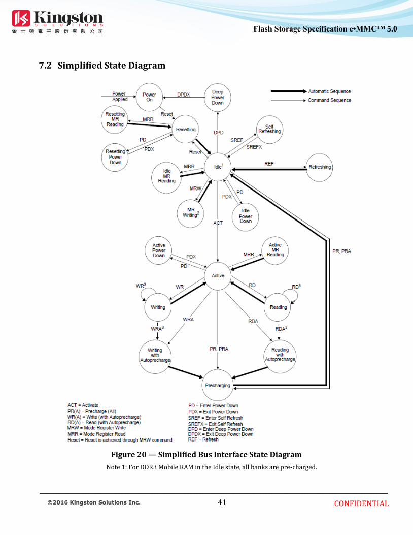
e•MMC™ 4.5 7.2 Simplified State Diagram
Figure 20 — Simplified Bus Interface State Diagram
Note 1: For DDR3 Mobile RAM in the Idle state, all banks are pre-charged.

____________________________________________________________________________________________________________________
CONFIDENTIAL
42 © 2016 Kingston Solutions Inc.
Flash Storage Specification e•MMC™ 5.0
Flash Storage Specification
e•MMC™ 4.5
Flash Storage Specification
e•MMC™ 4.5 7.3 Electrical Conditions
All voltages are referenced to VSS (GND) - Execute power-up and Initialization sequence before proper device operation is achieved. - Operation or timing that is not specified is illegal, and after such an event, in order to guarantee
proper operation, the DDR2 Mobile RAM Device must be powered down and then restarted through the specialized initialization sequence before normal operation can continue.
7.3.1 Absolute Maximum Ratings
Table 25 Absolute Maximum Ratings Parameter Symbol min. max. Unit Note
VDD1 supply voltage relative to VSS VDD1 -0.4 2.3 V 2
VDD2 supply voltage relative to VSS VDD2 -0.4 1.6 V 2
VDDCA supply voltage relative to VSSCA VDDCA -0.4 1.6 V 2, 3
VDDQ supply voltage relative to VSSQ VDDQ -0.4 1.6 V 2, 4
Voltage on any ball relative to VSS VIN, VOUT -0.4 1.6 V
Storage Temperature TSTG -55 125 °C 5
Notes: 1. Stresses greater than those listed under “Absolute Maximum Ratings” may cause permanent damage to the
device. This is a stress rating only and functional operation of the device at these or any other conditions above those indicated in the operational sections of this specification is not implied. Exposure to absolute maximum rating conditions for extended periods may affect reliability.
2. See Power-Ramp section “Power-up, initialization and Power-Off” on section7.6 for relationship between power supplies
3. VREFCA ≤ 0.6 x VDDCA; however, VREFCA may be ≥ VDDCA provided that VREFCA ≤ 300mV. 4. VREFDQ ≤ 0.7 × VDDQ; however, VREFDQ may be ≥ VDDQ provided that VREFDQ ≤ 300mV. 5. Storage Temperature is the case surface temperature on the center/top side of the DDR3 Mobile RAM Device.
Caution Exposing the device to stress above those listed in Absolute Maximum Ratings could cause permanent damage. The device is not meant to be operated under conditions outside the limits described in the operational section of this specification. Exposure to Absolute Maximum Rating conditions for extended periods may affect device reliability.
7.3.2 Recommended DC Operating Conditions
Table 26 Recommended DC Operating Conditions(TC = -25°C to +85°C) Parameter Symbol min. typ. max. Unit
Core Power1 VDD1 1.7 1.8 1.95 V
Core Power2, VDD2 1.14 1.2 1.3 V
Input Buffer Power VDDCA 1.14 1.2 1.3 V
I/O Buffer Power VDDQ 1.14 1.2 1.3 V

____________________________________________________________________________________________________________________
CONFIDENTIAL
43 © 2016 Kingston Solutions Inc.
Flash Storage Specification e•MMC™ 5.0
Flash Storage Specification
e•MMC™ 4.5
Flash Storage Specification
e•MMC™ 4.5 7.1.1 AC and DC Input Measurement Levels
7.1.1.1 AC and DC Input Levels for Single-Ended CA/CS Signals
Table 27 Single-Ended AC and DC Input Levels for CA/CS Inputs
Parameter Symbol Speed min. max. Unit Note
AC input logic high VIHCA(AC) 1333 / 1600 VREF + 0.150 Note 2 V 1, 2
AC input logic low VILCA(AC) 1333 / 1600 Note 2 VREF – 0.150 V 1, 2
DC input logic high VIHCA(DC) 1333 / 1600 VREF + 0.100 VDD2 V 1
DC input logic low VILCA(DC) 1333 / 1600 VSS VREF – 0.100 V 1
Reference Voltage for CA/CS inputs VREFCA(DC) 1333 / 1600 0.49 × VDD2 0.51 × VDD2 V 3, 4
Notes: 1. For CA/CS input only pins. VREF = VREFCA(DC). 2. See “Overshoot and Undershoot Specifications” on section 7.3.11. 3. The ac peak noise on VREFCA may not allow VREFCA to deviate from VREFCA(DC) by more than ± 1% VDD2 (for
reference: 43dditio. ± 12 mV). 4. For reference: 43dditio. VDD2/2 ± 12 mV.
7.1.1.2 AC and DC Input Levels for CKE
Parameter Symbol min. max. Unit Note
CKE Input High Level VIHCKE 0.65 × VDD2 Note 1 V 1
CKE Input Low Level VILCKE Note 1 0.35 × VDD2 V 1
Table 28 Single-Ended AC and DC Input Levels for CKE Note: 1. See “Overshoot and Undershoot Specifications” on section 7.3.11.
7.1.1.3 AC and DC Input Levels for Single-Ended Data Signals
Table 29 Single-Ended AC and DC Input Levels for DQ and DM Parameter Symbol Speed min. max. Unit Note
AC input logic high VIHDQ(AC) 1333/1600 VREF + 0.150 Note 2 V 1, 2 ,5
AC input logic low VILDQ(AC) 1333/1600 Note 2 VREF – 0.150 V 1, 2 ,5
DC input logic high VIHDQ(DC) 1333/1600 VREF + 0.100 VDDQ V 1
DC input logic low VILDQ(DC) 1333/1600 VSSQ VREF – 0.100 V 1
Reference Voltage for DQ, DM inputs VREFDQ(DC) (DQ ODT disable)
1333/1600 0.49 × VDDQ 0.51 × VDDQ V 3, 4
Reference Voltage for DQ, DM inputs VREFDQ(DC) (DQ ODT enable)
1333/1600 VODTR/2 –
0.01 * VDDQ VODTR/2 +
0.01 * VDDQ V 3,5,6
1. For DQ input only pins. VREF = VREFDQ(DC). 2. See “Overshoot and Undershoot Specifications” on section 7.3.11. 3. The ac peak noise on VREFDQ may not allow VREFDQ to deviate from VREFDQ(DC) by more than ± 1% VDDQ (for
reference: dditio. ± 12 mV). 4. For reference: 43alibra. VDDQ/2 +/- 12 mV. 5. For reference: 43alibra. VODTR/2 +/- 12 mV. 6. The nominal mode register programmed value for RODT and the nominal controller output impedance RON are used
for the calculation of VODTR. For testing purposes a controller RON value of 50 Ω is used.

____________________________________________________________________________________________________________________
CONFIDENTIAL
44 © 2016 Kingston Solutions Inc.
Flash Storage Specification e•MMC™ 5.0
Flash Storage Specification
e•MMC™ 4.5
Flash Storage Specification
e•MMC™ 4.5 7.1.2 VREF Tolerances
The dc-tolerance limits and ac-noise limits for the reference voltages VREFCA and VREFDQ are illustrated in Figure 21. It shows a valid reference voltage VREF(t) as a function of time. (VREF stands for VREFCA and VREFDQ likewise). VDD stands for VDD2 for VREFCA and VDDQ for VREFDQ. VREF(DC) is the linear average of VREF(t) over a very long period of time (e.g. 1 sec) and is specified as a fraction of the linear average of VDDQ or VDD2 also over a very long period of time (e.g. 1 sec). This average has to meet the min/max requirements in Table 28. Furthermore VREF(t) may temporarily deviate from VREF(DC) by no more than ± 1% VDD. VREF(t) cannot track noise on VDDQ or VDD2 if this would send VREF outside these specification.
Figure 21 — Illustration of VREF(DC) Tolerance and VREF AC-noise Limits
The voltage levels for setup and hold time measurements VIH(AC), VIH(DC), VIL(AC) and VIL(DC) are dependent on VREF.“VREF “ shall be understood as VREF(DC), as defined in Figure 21. This clarifies that dc-variations of VREF affect the absolute voltage a signal has to reach to achieve a valid high or low level and therefore the time to which setup and hold is measured. Devices will function correctly with appropriate timing deratings with VREF outside these specified levels so long as VREF is maintained between 0.44 × VDDQ (or VDD2) and 0.56 × VDDQ (or VDD2) and so long as the controller achieves the required single-ended AC and DC input levels from instantaneous VREF . Therefore, system timing and voltage budgets need to account for VREF deviations outside of this range. This also clarifies that the DRAM setup/hold specification and derating values need to include time and voltage associated with VREF AC-noise. Timing and voltage effects due to AC-noise on VREF up to the specified limit (± 1% of VDD) are included in DRAM timings and their associated deratings.

____________________________________________________________________________________________________________________
CONFIDENTIAL
45 © 2016 Kingston Solutions Inc.
Flash Storage Specification e•MMC™ 5.0
Flash Storage Specification
e•MMC™ 4.5
Flash Storage Specification
e•MMC™ 4.5 7.1.3 Input Signal
Figure 22 — LPDDR3 Input Signal
Notes: 1. Numbers reflect nominal values. 2. For CA0-9, CK_t, CK_c,and CS_n, VDD stands for VDDCA. For DQ, DM, DQS_t, and DQS_c, VDD stands for VDDQ 3. For CA0-9, CK_t, CK_c, and CS_n, VSS stands for VSSCA. For DQ, DM, DQS_t, and DQS_c, VSS stands for VSSQ.

____________________________________________________________________________________________________________________
CONFIDENTIAL
46 © 2016 Kingston Solutions Inc.
Flash Storage Specification e•MMC™ 5.0
Flash Storage Specification
e•MMC™ 4.5
Flash Storage Specification
e•MMC™ 4.5 AC and DC Logic Input Levels for Differential Signals
7.1.3.1 Differential Signal Definition
Figure 23 — Definition of Differential AC-swing and “Time above AC-level” tDVAC 7.1.3.2 Differential Swing Requirements for Clock (CK_t – CK_c) and Strobe (DQS_t –
DQS_c)
Table 32 Differential AC and DC Input Levels Parameter Symbol min. max. Unit Note
Differential input high VIHdiff(DC) 2 × (VIH(DC) – VREF) Note 3 V 1 Differential input low VILdiff(DC) Note 3 2 × (VIL(DC) – VREF) V 1 Differential input high AC VIHdiff(AC) 2 × (VIH(AC) – VREF) Note 3 V 2 Differential input low AC VILdiff(AC) Note 3 2 × (VIL(AC) – VREF) V 2
Notes: 1. Used to define a differential signal slew-rate. For CK_t – CK_c use VIH/VIL(dc) of CA and VREFCA; for DQS_t –
DQS_c, use VIH/VIL(dc) of DQs and VREFDQ; if a reduced dc-high or dc-low level is used for a signal group, then the reduced level applies also here.
2. For CK_t – CK_c use VIH/VIL(ac) of CA and VREFCA; for DQS_t – DQS_c, use VIH/VIL(ac) of DQs and VREFDQ; if a reduced ac-high or ac-low level is used for a signal group, then the reduced level applies also here.
3. These values are not defined, however the single-ended signals CK_t, CK_c, DQS_t, and DQS_c need to be within the respective limits (VIH(dc) max, VIL(dc)min) for single-ended signals as well as the limitations for overshoot and undershoot
4. For CK_t and CK_c, Vref = VrefCA(DC). For DQS_t and DQS_c, Vref = VrefDQ(DC).

____________________________________________________________________________________________________________________
CONFIDENTIAL
47 © 2016 Kingston Solutions Inc.
Flash Storage Specification e•MMC™ 5.0
Flash Storage Specification
e•MMC™ 4.5
Flash Storage Specification
e•MMC™ 4.5 Table 33 Allowed Time Before Ringback (tDVAC) for CK_t – CK_c and DQS_t – DQS_c
Slew Rate [V/ns]
tDVAC [ps] @ |VIH/Ldiff(ac)| = 300mV
1333Mbps
tDVAC [ps] @ |VIH/Ldiff(ac)| = 300mV
1600Mbp
min. min.
> 4.0 58 48
8.0 58 48
7.0 56 46
6.0 53 43
5.0 50 40
4.0 45 35
3.0 37 27
< 3.0 37 27
7.1.3.3 Single-ended Requirements for Differential Signals
Each individual component of a differential signal (CK_t, DQS_t, CK_c, or DQS_c) has also to comply with certain requirements for single-ended signals.
CK_t and CK_c shall meet VSEH(ac)min / VSEL(ac)max in every half-cycle.
DQS_t, DQS_c shall meet VSEH(ac)min / VSEL(ac)max in every half-cycle preceeding and following a valid transition. Note that the applicable ac-levels for CA and DQ’s are different per speed-bin.
Figure 24 — Single-ended Requirement for Differential Signals.
Note that while CA and DQ signal requirements are with respect to VREF, the single-ended components of differential signals have a requirement with respect to VDDQ/2 for DQS_t, DQS_c and VDDCA/2 for CK_t, CK_c; this is nominally the same. The transition of single-ended signals through the AC-levels is used to measure setup time. For single-ended components of differential signals the requirement to reach VSEL(AC)max, VSEH(AC)min has no bearing on timing, but adds a restriction on the common mode characteristics of these signals. The signal ended requirements for CK_t, CK_c, DQS_t and DQS_c are found in tables 3 and 5, respectively.

____________________________________________________________________________________________________________________
CONFIDENTIAL
48 © 2016 Kingston Solutions Inc.
Flash Storage Specification e•MMC™ 5.0
Flash Storage Specification
e•MMC™ 4.5
Flash Storage Specification
e•MMC™ 4.5
Table 34 Single-ended Levels for CK_t, DQS_t, CK_c, DQS_c Parameter Symbol min. max. Unit Note
Single-ended high-level for strobes
VSEH(AC150)
(VDDQ / 2) + 0.150 Note 3 V 1, 2
Single-ended high-level for CK_t, CK_c
(VDDCA / 2) + 0.150 Note 3 V 1, 2
Single-ended low-level for strobes
VSEL(AC150) Note 3 (VDDQ / 2) – 0.150 V 1, 2
Single-ended low-level for CK_t, CK_c
Note 3 (VDDCA / 2) – 0.150 V 1, 2
Single-ended high-level for strobes
VSEH(AC135)
(VDDQ / 2) + 0.135 Note 3 V 1, 2
Single-ended high-level for CK_t, CK_c
(VDDCA / 2) + 0.135 Note 3 V 1, 2
Single-ended low-level for strobes
VSEL(AC135)
Note 3 (VDDQ / 2) – 0.135 V 1, 2
Single-ended low-level for CK_t, CK_c
Note 3 (VDDCA / 2) – 0.135 V 1, 2
Notes: 1. For CK_t, CK_c use VSEH/VSEL(AC) of CA; for strobes (DQS0_t, DQS0_c, DQS1_t, DQS1_c, DQS2_t, DQS2_c, DQS3_t,
DQS3_c) use VIH/VIL(AC) of DQs. 2. VIH(AC)/VIL(AC) for DQs is based on VREFDQ; VSEH(AC)/VSEL(AC) for CA is based on VREFCA; if a reduced
Achigh or AC-low level is used for a signal group, then the reduced level applies also here 3. These values are not defined, however the single-ended signals CK_t, CK_c, DQS0_t, DQS0_c, DQS1_t, DQS1_c,
DQS2_t, DQS2_c, DQS3_t, DQS3_c need to be within the respective limits (VIH(DC) max, VIL(DC)min) for single-ended signals as well as the limitations for overshoot and undershoot. Refer to “Overshoot and Undershoot Specifications” on section 7.3.11.
7.1.4 Differential Input Cross Point Voltage
To guarantee tight setup and hold times as well as output skew parameters with respect to clock and strobe, each cross point voltage of differential input signals (CK_t, CK_c and DQS_t, DQS_c) must meet the requirements in Table 35. The differential input cross point voltage VIX is measured from the actual cross point of true and complement signals to the midlevel between of VDD and VSS.
Figure 25 — VIX Definition

____________________________________________________________________________________________________________________
CONFIDENTIAL
49 © 2016 Kingston Solutions Inc.
Flash Storage Specification e•MMC™ 5.0
Flash Storage Specification
e•MMC™ 4.5
Flash Storage Specification
e•MMC™ 4.5
Table 35 Cross Point Voltage for Differential Input Signals (CK, DQS) Parameter Symbol min. max. Unit Note
Differential Input Cross Point Voltage relative to VDDCA/2 for CK_t, CK_c
VIXCA -120 120 mV 1, 2
Differential Input Cross Point Voltage relative to VDDQ/2 for DQS_t, DQS_c
VIXDQ -120 120 mV 1, 2
Notes: 1. The typical value of VIX(AC) is expected to be about 0.5 × VDD of the transmitting device, and VIX(AC) is
expected to track variations in VDD. VIX(AC) indicates the voltage at which differential input signals must cross. 2. For CK_t and CK_c, VREF = VREFCA(DC). For DQS_t and DQS_c, VREF = VREFDQ(DC).
7.1.5 Slew Rate Definitions for Single-Ended Input Signals
See “CA and CS_c Setup, Hold and Derating” for single-ended slew rate definitions for address and command signals. See “Data Setup, Hold and Slew Rate Derating” for single-ended slew rate definitions for data signals. 7.1.6 Slew Rate Definitions for Differential Input Signals
Input slew rate for differential signals (CK_t, CK_c and DQS_t, DQS_c) are defined and measured as shown in Table 31 and Figure 26.
Table 31 Differential Input Slew Rate Definition
Description Measured
Defined by from to
Differential input slew rate for rising edge (CK_t – CK_c and DQS_t – DQS_c).
VILdiffmax VIHdiffmin [VIHdiffmin – VILdiffmax] / DeltaTRdiff
Differential input slew rate for falling edge (CK_t – CK_c and DQS_t – DQS_c).
VIHdiffmin VILdiffmax [VIHdiffmin – VILdiffmax] / DeltaTFdiff
Note: 1. The differential signal (i.e. CK_t – CK_c and DQS_t – DQS_c) must be linear between these thresholds.
Figure 26 — Differential Input Slew Rate Definition for DQS_t, DQS_c and CK_t, CK_c

____________________________________________________________________________________________________________________
CONFIDENTIAL
50 © 2016 Kingston Solutions Inc.
Flash Storage Specification e•MMC™ 5.0
Flash Storage Specification
e•MMC™ 4.5
Flash Storage Specification
e•MMC™ 4.5
7.1.7 AC and DC Output Measurement Levels
7.1.7.1 Single Ended AC and DC Output Levels
Table 37 shows the output levels used for measurements of single ended signals.
Table 37 Single-ended AC and DC Output Levels Parameter Symbol Value Unit Note
DC output high measurement level (for IV curve linearity) VOH(DC) 0.9 × VDDQ V 1
DC output low measurement level (for IV curve linearity) VOL(DC) 0.1 × VDDQ V 2
DC output low measurement level (for IV curve linearity) VOL(DC)
ODT enabled
VDDQ x [0.1 + 0.9 x (RON / (RTT +
RON))] V 3
AC output high measurement level (for output slew rate) VOH(AC) VREFDQ + 0.12 V
AC output low measurement level (for output slew rate) VOL(AC) VREFDQ – 0.12 V
Output Leakage current (DQ, DM, DQS_t, DQS_c) (DQ, DQS_t, DQS_c are disabled; 0V . VOUT . VDDQ)
IOZ min. -5 μA
max. 5 μA
Delta RON between pull-up and pull-down for DQ/DM MMPUPD min. -15 %
max. 15 %
Notes: 1. IOH = -0.1mA. 2. IOL = 0.1mA 3. The min value is derived when using RTT, min and RON,max (+/- 30% uncalibrated, +/-15% calibrated).
7.1.7.2 Differential AC and DC Output Levels
Table 38 shows the output levels used for measurements of differential signals.
Table 38 Differential AC and DC Output Levels Parameter Symbol Value Unit Note
AC differential output high measurement level (for output SR)
VOHdiff(AC) +0.2 × VDDQ V 1
AC differential output low measurement level (for output SR)
VOLdiff(AC) -0.2 × VDDQ V 2
Notes: 1. IOH = -0.1mA 2. IOL = 0.1mA

____________________________________________________________________________________________________________________
CONFIDENTIAL
51 © 2016 Kingston Solutions Inc.
Flash Storage Specification e•MMC™ 5.0
Flash Storage Specification
e•MMC™ 4.5
Flash Storage Specification
e•MMC™ 4.5
7.1.7.3 Single Ended Output Slew Rate
With the reference load for timing measurements, output slew rate for falling and rising edges is defined and measured between VOL(AC) and VOH(AC) for single ended signals as shown in Table 39 and Figure 27.
Table 39 Single-ended Output Slew Rate Definition
Description Measured
Defined by from to
Single-ended output slew rate for rising edge VOL(AC) VOH(AC) [VOH(AC) – VOL(AC)] / DeltaTRse
Single-ended output slew rate for falling edge VOH(AC) VOL(AC) [VOH(AC) – VOL(AC)] / DeltaTFse
Figure 27 — Single Ended Output Slew Rate Definition
Table 40 Output Slew Rate (single-ended) Parameter Symbol min. max. Unit
Single-ended Output Slew Rate (RON = 40Ω ± 30%) SRQse 1.5 3.5 V/ns
Output slew-rate matching Ratio (Pull-up to Pull-down) 0.7 1.4
Remark: SR: Slew Rate, Q: Query Output (like in DQ, which stands for Data-in, Query-Output), se: Single-ended Signals
Notes: 1. Measured with output reference load. 2. The ratio of pull-up to pull-down slew rate is specified for the same temperature and voltage, over the
entire temperature and voltage range. For a given output, it represents the maximum difference between pull-up and pulldown drivers due to process variation.
3. The output slew rate for falling and rising edges is defined and measured between VOL(AC) and VOH(AC).
4. Slew rates are measured under normal SSO conditions, with 1/2 of DQ signals per data byte driving logic high and 1/2 of DQ signals per data byte driving logic low.

____________________________________________________________________________________________________________________
CONFIDENTIAL
52 © 2016 Kingston Solutions Inc.
Flash Storage Specification e•MMC™ 5.0
Flash Storage Specification
e•MMC™ 4.5
Flash Storage Specification
e•MMC™ 4.5 7.1.8 Differential Output Slew Rate
With the reference load for timing measurements, output slew rate for falling and rising edges is defined and measured between VOLdiff(AC) and VOHdiff(AC) for differential signals as shown in Table 41 and Figure 28.
Table 41 Differential Output Slew Rate Definition
Description Measured Defined by
from to
Differential output slew rate for rising edge VOLdiff(AC) VOHdiff(AC) [VOHdiff(AC) – VOLdiff(AC)] / DeltaTRdiff
Differential output slew rate for falling edge VOHdiff(AC) VOLdiff(AC) [VOHdiff(AC) – VOLdiff(AC)] / DeltaTFdiff
Note: 1. Output slew rate is verified by design and characterization, and may not be subject to production test.
Figure 28 — Differential Output Slew Rate Definition
Table 42 Differential Output Slew Rate Parameter Symbol min. max. Unit
Differential Output Slew Rate (RON = 40Ω ± 30%) SRQdiff 3.0 8.0 V/ns
Remark: SR: Slew Rate, Q: Query Output (like in DQ, which stands for Data-in, Query-Output), diff: Differential Signals
Notes: 1. Measured with output reference load. 2. The output slew rate for falling and rising edges is defined and measured between VOL(AC) and VOH(AC). 3. Slew rates are measured under normal SSO conditions, with 1/2 of DQ signals per data byte driving logic
high and 1/2 of DQ signals per data byte driving logic low.

____________________________________________________________________________________________________________________
CONFIDENTIAL
53 © 2016 Kingston Solutions Inc.
Flash Storage Specification e•MMC™ 5.0
Flash Storage Specification
e•MMC™ 4.5
Flash Storage Specification
e•MMC™ 4.5 7.1.9 Overshoot and Undershoot Specifications
Table 43 AC Overshoot/Undershoot Specification Parameter
1333 1600 Unit
Maximum peak amplitude allowed for overshoot area. Max. 0.35 V
Maximum peak amplitude allowed for undershoot area. Max. 0.35 V
Maximum overshoot area above VDD*1 . max. 0.12 0.10 V-ns
Maximum undershoot area below VSS*2 max. 0.12 0.10 V-ns
Notes: 1. For CA0 – CA9, CK_t, CK_c, CS_c, and CKE, VDD stands for VDD2. For DQ, DM, DQS_t, and DQS_c, VDD stands for
VDDQ 2. For CA0 – CA9, CK_t, CK_c, CS_c, and CKE, VSS stands for VSS. For DQ, DM, DQS_t, and DQS_c, VSS stands for VSSQ
3. Values are referenced from actual VDDQ, VDD2, VSSQ, and VSS levels.
Figure 29 — Overshoot and Undershoot Definition

____________________________________________________________________________________________________________________
CONFIDENTIAL
54 © 2016 Kingston Solutions Inc.
Flash Storage Specification e•MMC™ 5.0
Flash Storage Specification
e•MMC™ 4.5
Flash Storage Specification
e•MMC™ 4.5 7.1.10 RONPU and RONPD Resistor Definition
RONPU = (VDDQ – Vout)
ABS(Iout)
Note 1: This is under the condition that RONPD is turned off
RONPD = Vout
ABS(Iout)
Note 1: This is under the condition that RONPU is turned off
Chip in Drive Mode
Figure 30 — Output Driver: Definition of Voltages and Currents
7.1.10.1 RONPU and RONPD Characteristics with ZQ Calibration
Output driver impedance RON is defined by the value of the external reference resistor RZQ. Nominal RZQ is 240Ω.
Table 44 Output Driver DC Electrical Characteristics with ZQ Calibration RONNOM Resistor Vout min. nom. Max. Unit Note
34.3Ω RON34PD 0.5 × VDDQ 0.85 1.00 1.15 RZQ/7 1, 2, 3, 4
RON34PU 0.5 × VDDQ 0.85 1.00 1.15 RZQ/7 1, 2, 3, 4
40.0Ω RON40PD 0.5 × VDDQ 0.85 1.00 1.15 RZQ/6 1, 2, 3, 4
RON40PU 0.5 × VDDQ 0.85 1.00 1.15 RZQ/6 1, 2, 3, 4
48.0Ω RON48PD 0.5 × VDDQ 0.85 1.00 1.15 RZQ/5 1, 2, 3, 4
RON48PU 0.5 × VDDQ 0.85 1.00 1.15 RZQ/5 1, 2, 3, 4
Mismatch between pull-up and pull-down
MMPUPD
-15.00
15.00 % 1, 2, 3, 4, 5
Notes: 1. Across entire operating temperature range, after calibration. 2. RZQ = 240Ω 3. The tolerance limits are specified after calibration with fixed voltage and temperature. For behavior of the
tolerance limits if temperature or voltage changes after calibration, see following section on voltage and temperature sensitivity.
4. Pull-down and pull-up output driver impedances are recommended to be calibrated at 0.5 × VDDQ. 5. Mesaurement definition for mismatch between pull-up and pull-down,
MMPUPD: Measure RONPU and RONPD, both at 0.5 × VDDQ:

____________________________________________________________________________________________________________________
CONFIDENTIAL
55 © 2016 Kingston Solutions Inc.
Flash Storage Specification e•MMC™ 5.0
Flash Storage Specification
e•MMC™ 4.5
Flash Storage Specification
e•MMC™ 4.5 MMPUPD =
RONPU – RONPD ×100
RONNOM
For example, with MMPUPD max.= 15% and RONPD = 0.85, RONPU must be less than 1.0. 6. Output driver strength measured without ODT.
7.1.10.2 Output Driver Temperature and Voltage Sensitivity
If temperature and/or voltage change after calibration, the tolerance limits widen according to the Tables shown below.
Table 45 Output Driver Sensitivity Definition Resistor Vout min. max. Unit Note
RONPD 0.5 × VDDQ 85 – (dRONdT × |ΔT|) – (dRONdV × |ΔV|) 115 + (dRONdT × |ΔT|) + (dRONdV × |ΔV|) % 1, 2
RONPU
RTT 0.5 × VDDQ 85 – (dRTTdT × |ΔT|) – (dRTTdV × |ΔV|) 115 + (dRTTdT × |ΔT|) + (dRTTdV × |ΔV|) % 1, 2
Notes: 1. ΔT = T – T(@ calibration), ΔV = V – V(@ calibration) 2. dRONdT, dRONdV, dRTTdV and dRTTdT are not subject to production test but are verified by design and characterization
Table 46 Output Driver Temperature and Voltage Sensitivity
Parameter Symbol min. max. Unit
RON Temperature Sensitivity dRONdT 0 0.75 %/°C
RON Voltage Sensitivity dRONdV 0 0.20 %/mV
RTT Temperature Sensitivity dRTTdT 0 0.75 %/°C
RTT Voltage Sensitivity dRTTdV 0 0.20 %/mV
7.1.10.3 RONPU and RONPD Characteristics without ZQ Calibration
Output driver impedance RON is defined by design and characterization as default setting.
Table 47 Output Driver DC Electrical Characteristics Without ZQ Calibration RONNOM Resistor Vout min. nom. Max. Unit Note
34.3Ω RON34PD 0.5 × VDDQ 24 34.3 44.6 Ω 1
RON34PU 0.5 × VDDQ 24 34.3 44.6 Ω 1
40.0Ω RON40PD 0.5 × VDDQ 28 40 52 Ω 1
RON40PU 0.5 × VDDQ 28 40 52 Ω 1
48.0Ω RON48PD 0.5 × VDDQ 33.6 48 62.4 Ω 1
RON48PU 0.5 × VDDQ 33.6 48 62.4 Ω 1
60.0Ω (optional)
RON60PD 0.5 × VDDQ 42 60 78 Ω 1
RON60PU 0.5 × VDDQ 42 60 78 Ω 1
80.0Ω (optional)
RON80PD 0.5 × VDDQ 56 80 104 Ω 1
RON80PU 0.5 × VDDQ 56 80 104 Ω 1
Note: 1. Across entire operating temperature range, without calibration.

____________________________________________________________________________________________________________________
CONFIDENTIAL
56 © 2016 Kingston Solutions Inc.
Flash Storage Specification e•MMC™ 5.0
Flash Storage Specification
e•MMC™ 4.5
Flash Storage Specification
e•MMC™ 4.5 7.1.10.4 RZQ I-V Curve
Table 48 RZQ I-V Curve
Voltage[V]
RON = 240 Ω (RZQ)
Pull-Down Pull-Up
Current [mA] / RON [Ohms] Current [mA] / RON [Ohms]
default value after
ZQReset
with
Calibration default value after
ZQReset
with
Calibration
Min Max Min Max Min Max Min Max
[mA] [mA] [mA] [mA] [mA] [mA] [mA] [mA]
0.00 0.00 0.00 n/a n/a 0.00 0.00 n/a n/a
0.05 0.17 0.35 n/a n/a -0.17 -0.35 n/a n/a
0.10 0.34 0.70 n/a n/a -0.34 -0.70 n/a n/a
0.15 0.50 1.03 n/a n/a -0.50 -1.03 n/a n/a
0.20 0.67 1.39 n/a n/a -0.67 -1.39 n/a n/a
0.25 0.83 1.73 n/a n/a -0.83 -1.73 n/a n/a
0.30 0.97 2.05 n/a n/a -0.97 -2.05 n/a n/a
0.35 1.13 2.39 n/a n/a -1.13 -2.39 n/a n/a
0.40 1.26 2.71 n/a n/a -1.26 -2.71 n/a n/a
0.45 1.39 3.01 n/a n/a -1.39 -3.01 n/a n/a
0.50 1.51 3.32 n/a n/a -1.51 -3.32 n/a n/a
0.55 1.63 3.63 n/a n/a -1.63 -3.63 n/a n/a
0.60 1.73 3.93 2.17 2.94 -1.73 -3.93 -2.17 -2.94
0.65 1.82 4.21 n/a n/a -1.82 -4.21 n/a n/a
0.70 1.90 4.49 n/a n/a -1.90 -4.49 n/a n/a
0.75 1.97 4.74 n/a n/a -1.97 -4.74 n/a n/a
0.80 2.03 4.99 n/a n/a -2.03 -4.99 n/a n/a
0.85 2.07 5.21 n/a n/a -2.07 -5.21 n/a n/a
0.90 2.11 5.41 n/a n/a -2.11 -5.41 n/a n/a
0.95 2.13 5.59 n/a n/a -2.13 -5.59 n/a n/a
1.00 2.17 5.72 n/a n/a -2.17 -5.72 n/a n/a
1.05 2.19 5.84 n/a n/a -2.19 -5.84 n/a n/a
1.10 2.21 5.95 n/a n/a -2.21 -5.95 n/a n/a
1.15 2.23 6.03 n/a n/a -2.23 -6.03 n/a n/a
1.20 2.25 6.11 n/a n/a -2.25 -6.11 n/a n/a
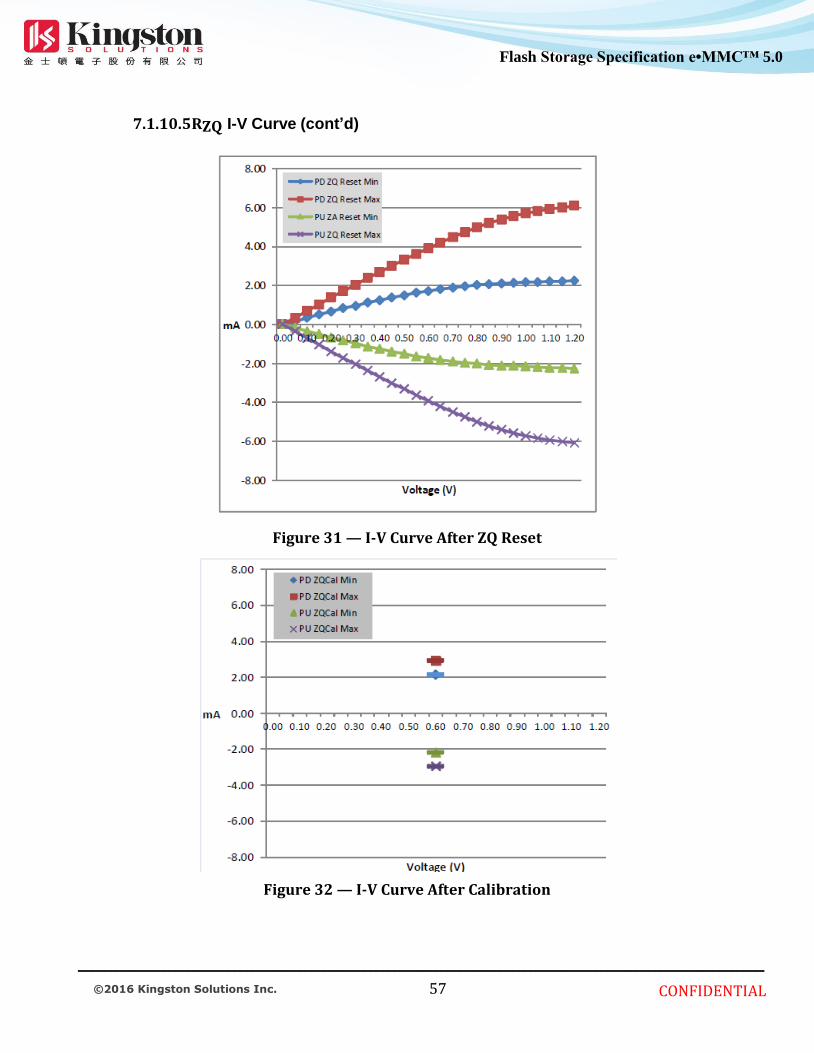
____________________________________________________________________________________________________________________
CONFIDENTIAL
57 © 2016 Kingston Solutions Inc.
Flash Storage Specification e•MMC™ 5.0
Flash Storage Specification
e•MMC™ 4.5
Flash Storage Specification
e•MMC™ 4.5 7.1.10.5 RZQ I-V Curve (cont’d)
Figure 31 — I-V Curve After ZQ Reset
Figure 32 — I-V Curve After Calibration

____________________________________________________________________________________________________________________
CONFIDENTIAL
58 © 2016 Kingston Solutions Inc.
Flash Storage Specification e•MMC™ 5.0
Flash Storage Specification
e•MMC™ 4.5
Flash Storage Specification
e•MMC™ 4.5 7.1.10.6 ODT Levels and I-V Characteristics
On-Die Termination effective resistance, RTT, is defined by mode register MR11[1:0]. ODT is applied to the DQ, DM, and DQS_t/DQS_c pins. A functional representation of the on-die termination is shown Figure 33 RTT is defined by the following formula: RTTPU = (VDDQ – Vout) / | Iout |
Figure 33 — Functional representation of On-Die Termination
Table 49 –
ODT DC Electrical Characteristics, assuming RZQ = 240 ohm after proper ZQ calibration
RTT (ohm) VOUT (V)
IOUT
Min
(mA)
Max
(ma)
RZQ/1 0.6 -2.17 -2.94
RZQ/2 0.6 -4.34 -5.88
RZQ/4 0.6 -8.68 -11.76
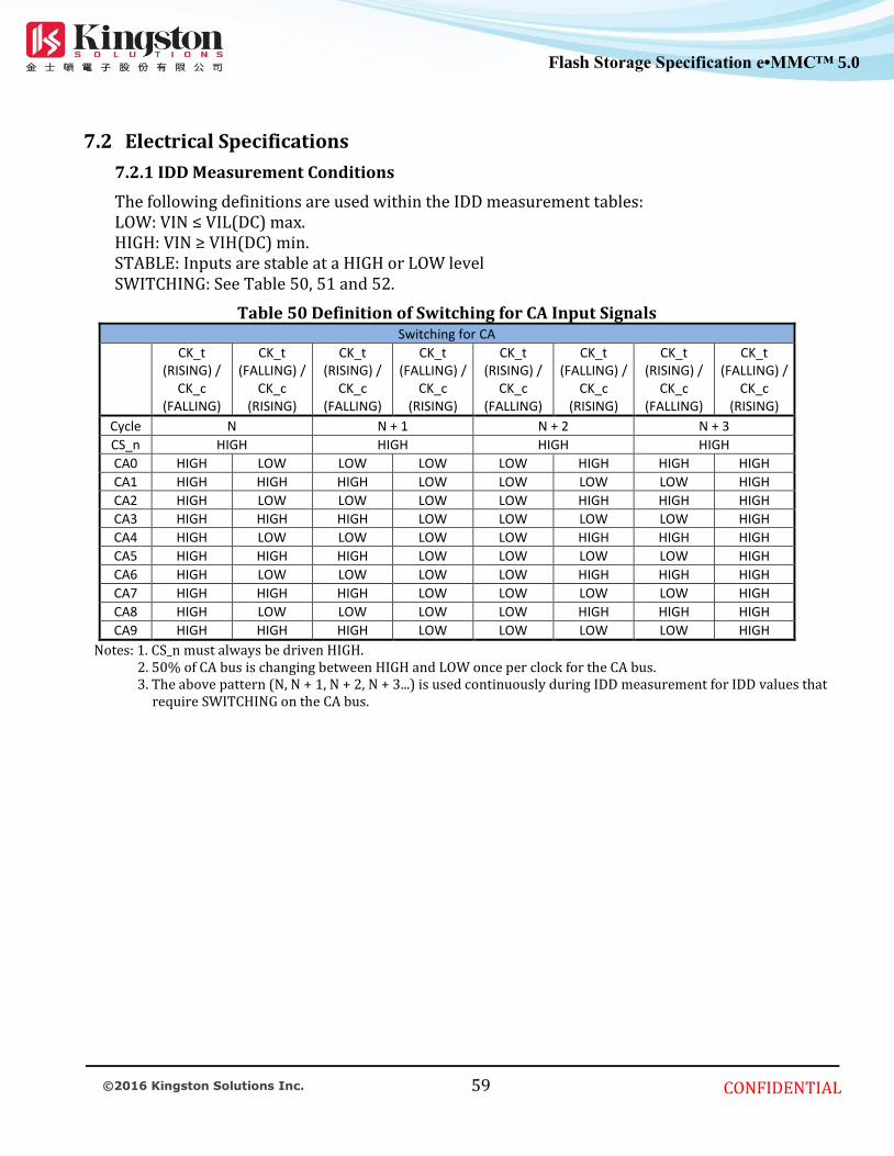
____________________________________________________________________________________________________________________
CONFIDENTIAL
59 © 2016 Kingston Solutions Inc.
Flash Storage Specification e•MMC™ 5.0
Flash Storage Specification
e•MMC™ 4.5
Flash Storage Specification
e•MMC™ 4.5 7.2 Electrical Specifications
7.2.1 IDD Measurement Conditions
The following definitions are used within the IDD measurement tables: LOW: VIN ≤ VIL(DC) max. HIGH: VIN ≥ VIH(DC) min. STABLE: Inputs are stable at a HIGH or LOW level SWITCHING: See Table 50, 51 and 52.
Table 50 Definition of Switching for CA Input Signals Switching for CA
CK_t (RISING) /
CK_c (FALLING)
CK_t (FALLING) /
CK_c (RISING)
CK_t (RISING) /
CK_c (FALLING)
CK_t (FALLING) /
CK_c (RISING)
CK_t (RISING) /
CK_c (FALLING)
CK_t (FALLING) /
CK_c (RISING)
CK_t (RISING) /
CK_c (FALLING)
CK_t (FALLING) /
CK_c (RISING)
Cycle N N + 1 N + 2 N + 3
CS_n HIGH HIGH HIGH HIGH
CA0 HIGH LOW LOW LOW LOW HIGH HIGH HIGH
CA1 HIGH HIGH HIGH LOW LOW LOW LOW HIGH
CA2 HIGH LOW LOW LOW LOW HIGH HIGH HIGH
CA3 HIGH HIGH HIGH LOW LOW LOW LOW HIGH
CA4 HIGH LOW LOW LOW LOW HIGH HIGH HIGH
CA5 HIGH HIGH HIGH LOW LOW LOW LOW HIGH
CA6 HIGH LOW LOW LOW LOW HIGH HIGH HIGH
CA7 HIGH HIGH HIGH LOW LOW LOW LOW HIGH
CA8 HIGH LOW LOW LOW LOW HIGH HIGH HIGH
CA9 HIGH HIGH HIGH LOW LOW LOW LOW HIGH
Notes: 1. CS_n must always be driven HIGH. 2. 50% of CA bus is changing between HIGH and LOW once per clock for the CA bus. 3. The above pattern (N, N + 1, N + 2, N + 3...) is used continuously during IDD measurement for IDD values that
require SWITCHING on the CA bus.

____________________________________________________________________________________________________________________
CONFIDENTIAL
60 © 2016 Kingston Solutions Inc.
Flash Storage Specification e•MMC™ 5.0
Flash Storage Specification
e•MMC™ 4.5
Flash Storage Specification
e•MMC™ 4.5 Table 51 Definition of Switching for IDD4R
Clock CKE CS_n Clock Cycle Number Command CA0 – CA2 CA3 – CA9 All DQ
Rising HIGH LOW N Read_Rising HLH LHLHLHL L
Falling HIGH LOW N Read_Falling LLL LLLLLLL L
Rising HIGH HIGH N + 1 NOP LLL LLLLLLL H
Falling HIGH HIGH N + 1 NOP LLL LLLLLLL L
Rising HIGH HIGH N + 2 NOP LLL LLLLLLL H
Falling HIGH HIGH N + 2 NOP LLL LLLLLLL H
Rising HIGH HIGH N + 3 NOP LLL LLLLLLL H
Falling HIGH HIGH N + 3 NOP HLH HLHLLHL L
Rising HIGH LOW N + 4 Read_Rising HLH HLHLLHL H
Falling HIGH LOW N + 4 Read_Falling LHH HHHHHHH H
Rising HIGH HIGH N + 5 NOP HHH HHHHHHH H
Falling HIGH HIGH N + 5 NOP HHH HHHHHHH L
Rising HIGH HIGH N + 6 NOP HHH HHHHHHH L
Falling HIGH HIGH N + 6 NOP HHH HHHHHHH L
Rising HIGH HIGH N + 7 NOP HHH HHHHHHH H
Falling HIGH HIGH N + 7 NOP HLH LHLHLHL L
Notes: 1. Data strobe (DQS) is changing between HIGH and LOW every clock cycle. 2. The above pattern (N, N + 1...) is used continuously during IDD measurement for IDD4R.

____________________________________________________________________________________________________________________
CONFIDENTIAL
61 © 2016 Kingston Solutions Inc.
Flash Storage Specification e•MMC™ 5.0
Flash Storage Specification
e•MMC™ 4.5
Flash Storage Specification
e•MMC™ 4.5
Table 52 Definition of Switching for IDD4W Clock CKE /CS Clock Cycle Number Command CA0 – CA2 CA3 – CA9 All DQ
Rising HIGH LOW N Read_Rising HLL LHLHLHL L
Falling HIGH LOW N Read_Falling LLL LLLLLLL L
Rising HIGH HIGH N + 1 NOP LLL LLLLLLL H
Falling HIGH HIGH N + 1 NOP LLL LLLLLLL L
Rising HIGH HIGH N + 2 NOP LLL LLLLLLL H
Falling HIGH HIGH N + 2 NOP LLL LLLLLLL H
Rising HIGH HIGH N + 3 NOP LLL LLLLLLL H
Falling HIGH HIGH N + 3 NOP HLL HLHLLHL L
Rising HIGH LOW N + 4 Read_Rising HLL HLHLLHL H
Falling HIGH LOW N + 4 Read_Falling LHH HHHHHHH H
Rising HIGH HIGH N + 5 NOP HHH HHHHHHH H
Falling HIGH HIGH N + 5 NOP HHH HHHHHHH L
Rising HIGH HIGH N + 6 NOP HHH HHHHHHH L
Falling HIGH HIGH N + 6 NOP HHH HHHHHHH L
Rising HIGH HIGH N + 7 NOP HHH HHHHHHH H
Falling HIGH HIGH N + 7 NOP HLL LHLHLHL L
Notes: 1. Data strobe (DQS) is changing between HIGH and LOW every clock cycle. 2. Data masking (DM) must always be driven LOW. 3. The above pattern (N, N + 1...) is used continuously during IDD measurement for IDD4W.

____________________________________________________________________________________________________________________
CONFIDENTIAL
62 © 2016 Kingston Solutions Inc.
Flash Storage Specification e•MMC™ 5.0
Flash Storage Specification
e•MMC™ 4.5
Flash Storage Specification
e•MMC™ 4.5 7.2.2 IDD Specifications
IDD values are for the entire operating voltage range, and all of them are for the entire standard range, with the exception of IDD6ET which is for the entire extended temperature range
Table 53 — IDD Specification Parameters and Operating Conditions
Parameter/Condition Symbol Power Supply Notes
Active power-down standby current with clock stop: CK = LOW, CK# = HIGH;
CKE is LOW;
CS_n is HIGH; One bank is active;
CA bus inputs are stable; Data bus inputs are stable ODT disabled
IDD3PS1 VDD1
IDD3PSS2 VDD2
IDD3PS,in
VDDCA, VDDQ
4
Active non-power-down standby current:
tCK = tCKmin; CKE is HIGH;
CS_n is HIGH; One bank is active;
CA bus inputs are switching; Data bus inputs are stable
ODT disabled
IDD3N1
VDD1
IDD3N2
VDD2
IDD3N,in
VDDCA, VDDQ
4
Active non-power-down standby current with clock stopped: CK = LOW, CK# = HIGH
CKE is HIGH;
CS_n is HIGH; One bank is active;
CA bus inputs are stable;
Data bus inputs are stable ODT disabled
IDD3NS1 VDD1
IDD3NS2 VDD2
IDD3NS,in
VDDCA, VDDQ
4
Operating burst READ current:
tCK = tCKmin;
CS_n is HIGH between valid commands;
One bank is active;
BL = 8; RL = RL (MIN);
CA bus inputs are switching;
50% data change each burst transfer ODT disabled
IDD4R1 VDD1
IDD4R2 VDD2
IDD4R,in VDDCA
IDD4RQ
VDDQ
5

____________________________________________________________________________________________________________________
CONFIDENTIAL
63 © 2016 Kingston Solutions Inc.
Flash Storage Specification e•MMC™ 5.0
Flash Storage Specification
e•MMC™ 4.5
Flash Storage Specification
e•MMC™ 4.5
Operating burst WRITE current:
tCK = tCKmin;
CS_n is HIGH between valid commands;
One bank is active;
BL = 8; WL = Wlmin;
CA bus inputs are switching;
50% data change each burst transfer
ODT disabled
IDD4W1 VDD1
IDD4W2 VDD2
IDD4W,in
VDDCA, VDDQ
4
All-bank REFRESH burst current:
tCK = tCKmin;
CKE is HIGH between valid commands;
tRC = tRFCabmin; Burst refresh;
CA bus inputs are switching; Data bus inputs are stable ODT disabled
IDD51 VDD1
IDD52 VDD2
IDD5IN
VDDCA, VDDQ
4
Table 54 — IDD Specification Parameters and Operating Conditions (cont’d)
Parameter/Condition Symbol Power Supply Notes
All-bank REFRESH average current:
tCK = tCKmin;
CKE is HIGH between valid commands;
tRC = tREFI;
CA bus inputs are switching;
Data bus inputs are stable ODT disabled
IDD5AB1 VDD1
IDD5AB2 VDD2
IDD5AB,in
VDDCA, VDDQ
4
Per-bank REFRESH average current:
tCK = tCKmin;
CKE is HIGH between valid commands;
tRC = tREFI/8;
CA bus inputs are switching;
Data bus inputs are stable ODT disabled
IDD5PB1 VDD1
IDD5PB2 VDD2
IDD5PB,in
VDDCA, VDDQ
4
Self refresh current (–25°C to +85°C): CK_t = LOW, CK_c = HIGH;
CKE is LOW;
CA bus inputs are stable;
IDD61 VDD1 6, 7, 9

____________________________________________________________________________________________________________________
CONFIDENTIAL
64 © 2016 Kingston Solutions Inc.
Flash Storage Specification e•MMC™ 5.0
Flash Storage Specification
e•MMC™ 4.5
Flash Storage Specification
e•MMC™ 4.5
Data bus inputs are stable
Maximum 1x self refresh rate ODT disabled
IDD62 VDD2 6, 7, 9
IDD6IN
VDDCA, VDDQ
4, 6, 7, 9
Self refresh current (+85°C ):
CK_t = LOW, CK_c = HIGH;
CKE is LOW;
CA bus inputs are stable; Data bus inputs are stable
ODT disabled
IDD6ET1 VDD1 7, 8, 9
IDD6ET2 VDD2 7, 8, 9
IDD6ET,in
VDDCA, VDDQ
4, 7, 8, 9
Deep power-down current: CK_t = LOW, CK_c = HIGH; CKE is LOW;
CA bus inputs are stable; Data bus inputs are stable ODT disabled
IDD81 VDD1
IDD82 VDD2
IDD8IN
VDDCA, VDDQ
4
NOTE:
1. Published IDD values are the maximum of the distribution of the arithmetic mean.
2. ODT disabled: MR11[2:0] = 000B.
3. IDD current specifications are tested after the device is properly initialized.
4. Measured currents are the summation of VDDQ and VDDCA.
5. Guaranteed by design with output load = 5 pF and RON = 40 ohm.
6. The 1x self refresh rate is the rate at which the device is refreshed internally during self refresh, before
going into the elevated temperature range.
7. This is the general definition that applies to full-array SELF REFRESH.
8. IDD6ET is a typical value, is sampled only, and is not tested.
9. Supplier datasheets may contain additional Self-Refresh IDD values for temperature subranges within
the standard or elevated temperature ranges.
10. For all IDD measurements, VIHCKE = 0.8 x VDDCA, VILCKE = 0.2 x VDDCA.
7.2.3 IDD Specifications (cont’d)
Table 55 — IDD6 Partial Array Self-Refresh Current
Parameter Value Unit
IDD6 Partial Array Self-Refresh Current
Full Array - μA
1/2 Array - μA
1/4 Array - μA
1/8 Array - μA
NOTE:
1 IDD6 currents are measured using bank-masking only.
2 IDD values published are the maximum of the distribution of the arithmetic mean.

____________________________________________________________________________________________________________________
CONFIDENTIAL
65 © 2016 Kingston Solutions Inc.
Flash Storage Specification e•MMC™ 5.0
Flash Storage Specification
e•MMC™ 4.5
Flash Storage Specification
e•MMC™ 4.5 7.2.4 DC Characteristics 1
(TC = -25°C to +85°C, VDD1 = 1.70V to 1.95V, VDD2, VDDQ = 1.14V to 1.30V)
Table 56 IDD Specification Parameters and Operating Conditions
Symbol Power Supply
1600 Unit Parameter/Condition
SDP DDP
IDD0_1 VDD1 15 30 mA Operating one bank active-pecharge current: tCK = tCK(avg)min; tRC = tRCmin; CKE is HIGH; CS_n is HIGH between valid commands; CA bus inputs are SWITCHING; Data bus inputs are STABLE ODT disable
IDD0_2 VDD2 70 140 mA
IDD0_IN VDDCA VDDQ
12 24 mA
IDD2P_1 VDD1 600 1200 μA Idle power-down standby current: tCK = tCK(avg)min; CKE is LOW; CS_n is HIGH; All banks idle; CA bus inputs are SWITCHING; Data bus inputs are STABLE ODT disable
IDD2P_2 VDD2 800 1600 μA
IDD2P_IN VDDCA VDDQ
120 240 μA
IDD2PS_1 VDD1 600 1200 μA Idle power-down standby current with clock stop: CK = LOW, /CK = HIGH; CKE is LOW; CS_n is HIGH; All banks idle; CA bus inputs are STABLE; Data bus inputs are STABLE ODT disable
IDD2PS_2 VDD2 800 1600 μA
IDD2PS_IN VDDCA VDDQ
120 240 μA
IDD2N_1 VDD1 2 4 mA Idle non power-down standby current: tCK = tCK(avg)min; CKE is HIGH; CS_n is HIGH; All banks idle; CA bus inputs are SWITCHING; Data bus inputs are STABLE ODT disable
IDD2N_2 VDD2 24 48 mA
IDD2N_IN VDDCA VDDQ
12 24 mA
IDD2NS_1 VDD1 1.7 3.4 mA Idle non power-down standby current with clock stop: CK _t= LOW, CK_c = HIGH; CKE is HIGH; CS_n is HIGH; All banks idle; CA bus inputs are STABLE; Data bus inputs are STABLE ODT disable
IDD2NS_2 VDD2 10 20 mA
IDD2NS_IN VDDCA VDDQ
6 12 mA
IDD3P_1 VDD1 1000 2000 μA Active power-down standby current: tCK = tCK(avg)min; CKE is LOW; CS_n is HIGH; One bank active; CA bus inputs are SWITCHING; Data bus inputs are STABLE ODT disable
IDD3P_2 VDD2 7.5 15 mA
IDD3P_IN VDDCA VDDQ
150 300 μA
IDD3PS_1 VDD1 1300 2600 μA Active power-down standby current with clock stop: CK _t= LOW, CK_c = HIGH; CKE is LOW; CS_n is HIGH; One bank active; CA bus inputs are STABLE; Data bus inputs are STABLE ODT disable
IDD3PS_2 VDD2 7.5 15 mA
IDD3PS_IN VDDCA VDDQ
150 300 μA
IDD3N_1 VDD1 2 4 mA Active non power-down standby current:

____________________________________________________________________________________________________________________
CONFIDENTIAL
66 © 2016 Kingston Solutions Inc.
Flash Storage Specification e•MMC™ 5.0
Flash Storage Specification
e•MMC™ 4.5
Flash Storage Specification
e•MMC™ 4.5
IDD3N_2 VDD2 25 50 mA tCK = tCK(avg)min; CKE is HIGH; CS_n is HIGH; One bank active; CA bus inputs are SWITCHING; Data bus inputs are STABLE ODT disable
IDD3N_IN VDDCA VDDQ
12 24 mA
IDD3NS_1 VDD1 2 4 mA Active non power-down standby current with clock stop: CK_t = LOW, CK_c = HIGH; CKE is HIGH; /CS is HIGH; One bank active; CA bus inputs are STABLE; Data bus inputs are STABLE ODT disable
IDD3NS_2 VDD2 20 40 mA
IDD3NS_IN VDDCA VDDQ
6 12 mA
Table 57 IDD Specification Parameters and Operating Conditions (cont’d)
Symbol Power Supply
1600 Unit Parameter/Condition
SDP DDP
IDD4R_1 VDD1 3 6 mA Operating burst read current: tCK = tCK(avg)min; CS_n is HIGH between valid commands; One bank active; BL = 4; RL = Rlmin; CA bus inputs are SWITCHING; 50% data change each burst transfer; ODT disable
IDD4R_2 VDD2 250 500 mA
IDD4R_IN VDDCA 12 24 mA
IDD4W_1 VDD1 3 6 mA Operating burst write current: tCK = tCK(avg)min; CS_n is HIGH between valid commands; One bank active; BL = 4; WL = Wlmin; CA bus inputs are SWITCHING; 50% data change each burst transfer; ODT disable;
IDD4W_2 VDD2 250 500 mA
IDD4W_IN VDDCA VDDQ
40 80 mA
IDD5_1 VDD1 20 40 mA All Bank Auto Refresh Burst current: tCK = tCK(avg)min; CKE is HIGH between valid commands; tRC = tRFCabmin; Burst refresh; CA bus inputs are SWITCHING; Data bus inputs are STABLE; ODT disable
IDD5_2 VDD2 150 300 mA
IDD5_IN VDDCA VDDQ
12 24 mA
IDD5AB_1 VDD1 5 10 mA All Bank Auto Refresh Average current: tCK = tCK(avg)min; CKE is HIGH between valid commands; tRC = tREFI; CA bus inputs are SWITCHING; Data bus inputs are STABLE; ODT disable
IDD5AB_2 VDD2 25 50 mA
IDD5AB_IN VDDCA VDDQ
12 24 mA
IDD5PB_1 VDD1 5 10 mA Per Bank Auto Refresh Average current: tCK = tCK(avg)min; CKE is HIGH between valid commands; tRC = tREFI/8; CA bus inputs are SWITCHING; Data bus inputs are STABLE; ODT disable
IDD5PB_2 VDD2 25 50 mA
IDD5PB_IN VDDCA VDDQ
12 24 mA
Notes: 1. IDD values published are the maximum of the distribution of the arithmetic mean. 2. IDD current specifications are tested after the device is properly initialized.

____________________________________________________________________________________________________________________
CONFIDENTIAL
67 © 2016 Kingston Solutions Inc.
Flash Storage Specification e•MMC™ 5.0
Flash Storage Specification
e•MMC™ 4.5
Flash Storage Specification
e•MMC™ 4.5 Table 58 IDD6 Full and Partial Array Self-Refresh Current
Parameter Symbol SDP Value DDP Value Unit Condition
Self-Refresh Current
TC ≦ +85°C Full Array
IDD6_1 1000 2000 μA CK _t= LOW, CK_c = HIGH; CKE is LOW; CA bus inputs are STABLE; Data bus inputs are STABLE;
IDD6_2 4000 8000 μA
IDD6_IN 120 240 μA
1/2 Array
IDD6_1 950 1900 μA
IDD6_2 2300 4600 μA
IDD6_IN 120 240 μA
1/4 Array
IDD6_1 900 1800 μA
IDD6_2 1500 3000 μA
IDD6_IN 120 240 μA
1/8 Array
IDD6_1 850 1700 μA
IDD6_2 1060 2120 μA
IDD6_IN 120 240 μA
Note: 1. IDD6 85°C is the maximum of the distribution of the arithmetic mean.
7.2.5 DC Characteristics 2
(TC = -25°C to +85°C, VDD1 = 1.70V to 1.95V, VDD2, VDDQ = 1.14V to 1.30V)
Table 59 Electrical Characteristics and Operating Conditions Symbol min. max. Unit Parameter/Condition Note
IL -2 2 μA
Input leakage current: For CA, CKE, CS_n, CK_t, CK_c Any input 0V <VIN < VDDCA (All other pins not under test = 0V)
2
IVREF -1 1 μA VREF supply leakage current: VREFDQ = VDDQ/2 or VREFCA = VDDCA/2 (All other pins not under test = 0V)
1
Notes: 1. The minimum limit requirement is for testing purposes. The leakage current on VREFCA and VREFDQ pins
should be minimal. 2. Although DM is for input only, the DM leakage shall match the DQ and DQS_t, DQS_c output leakage
specification.

____________________________________________________________________________________________________________________
CONFIDENTIAL
68 © 2016 Kingston Solutions Inc.
Flash Storage Specification e•MMC™ 5.0
Flash Storage Specification
e•MMC™ 4.5
Flash Storage Specification
e•MMC™ 4.5
7.2.6 Pin Capacitance (For 4Gb)
(TA = +25°C, VDD1 = 1.70V to 1.95V, VDD2, VDDQ = 1.14V to 1.30V)
Table 60 Input/Output Capacitance Parameter Symbol min. max. Unit Note
Input capacitance, CK_t and CK_c CCK 0.5 1.2 pF 1, 2
Input capacitance delta, CK_t and CK_c CDCK 0 0.15 pF 1, 2, 3
Input capacitance, all other input-only pins CI 0.5 1.1 pF 1, 2, 4
Input capacitance delta, all other input-only pins CDI -0.2 0.2 pF 1, 2, 5
Input/output capacitance, DQ, DM, DQS_t, DQS_c CIO 1.0 1.8 pF 1, 2, 6, 7
Input/output capacitance delta, DQS_t, DQS_c CDDQS 0 0.2 pF 1, 2, 7, 8
Input/output capacitance delta, DQ, DM CDIO -0.25 0.25 pF 1, 2, 7, 9
Input/output capacitance ZQ Pin CZQ 0 2.0 pF 1, 2
Notes: 1. This parameter applies to die device only (does not include package capacitance) 2. This parameter is not subject to production test. It is verified by design and characterization. The capacitance is measured according to JEP147 (Procedure for measuring input capacitance using a vector network analyzer (VNA) with VDD1, VDD2, VDDQ, VSS, VSSQ applied and all other pins floating 3. Absolute value of CCK_t – CCK_c. 4. CI applies to CS_n, CKE, CA0 – CA9,ODT 5. CDI = CI – 0.5 × (CCK_t + CCK_c) 6. DM loading matches DQ and DQS 7. MR3 I/O configuration DS OP3-OP0 = 0001B (34.3 Ω typical) 8. Absolute value of CDQS_t and CDQS_c 9. CDIO = CIO – 0.5 × (CDQS_t + CDQS_c) in byte-lane.
7.2.7 Clock Specification
The jitter specified is a random jitter meeting a Gaussian distribution. Input clocks violating the min/max values may result in malfunction of the LPDDR3 device..
7.2.7.1 Definition for tCK(avg) and nCK tCK(avg) is calculated as the average clock period across any consecutive 200 cycle window, where each clock period is calculated from rising edge to rising edge.
Unit ‘tCK(avg)’ represents the actual clock average tCK(avg) of the input clock under operation. Unit ‘nCK’ represents one clock cycle of the input clock, counting the actual clock edges. tCK(avg) may change by up to +/-1% within a 100 clock cycle window, provided that all jitter and timing specs are met.
____________________________________________________________________________________________________________________
CONFIDENTIAL
69 © 2016 Kingston Solutions Inc.
Flash Storage Specification e•MMC™ 5.0
Flash Storage Specification
e•MMC™ 4.5
Flash Storage Specification
e•MMC™ 4.5 7.2.7.2 Definition for tCK(abs)
tCK(abs) is defined as the absolute clock period, as measured from one rising edge to the next consecutive rising edge. tCK(abs) is not subject to production test. 7.2.7.3 Definition for tCH(avg) and tCL(avg)
tCH(avg) is defined as the average high pulse width, as calculated across any consecutive 200 high pulses.
tCL(avg) is defined as the average low pulse width, as calculated across any consecutive 200 low pulses.
7.2.7.4 Definition for tJIT(per)
tJIT(per) is the single period jitter defined as the largest deviation of any signal tCK from tCK(avg). tJIT(per) = Min/max of {tCKi – tCK(avg) where I = 1 to 200}. tJIT(per),act is the actual clock jitter for a given system. tJIT(per),allowed is the specified allowed clock period jitter. tJIT(per) is not subject to production test. 7.2.7.5 Definition for tJIT(cc)
tJIT(cc) is defined as the absolute difference in clock period between two consecutive clock cycles. tJIT(cc) = Max of |{tCKi +1 – tCKi}|. tJIT(cc) defines the cycle to cycle jitter. tJIT(cc) is not subject to production test. 7.2.7.6 Definition for tERR(nper)
tERR(nper) is defined as the cumulative error across n multiple consecutive cycles from tCK(avg). tERR(nper), act is the actual clock jitter over n cycles for a given system. tERR(nper), allowed is the specified allowed clock period jitter over n cycles. tERR(nper) is not subject to production test.

____________________________________________________________________________________________________________________
CONFIDENTIAL
70 © 2016 Kingston Solutions Inc.
Flash Storage Specification e•MMC™ 5.0
Flash Storage Specification
e•MMC™ 4.5
Flash Storage Specification
e•MMC™ 4.5
tERR(nper),min can be calculated by the formula shown below:
tERR(nper), min = (1 + 0.68LN(n)) . tJIT(per), min
tERR(nper),max can be calculated by the formula shown below:
tERR(nper), max = (1 + 0.68LN(n)) . tJIT(per), max
Using these equations, tERR(nper) tables can be generated for each tJIT(per),act value. 7.2.7.7 Definition for Duty Cycle Jitter tJIT(duty)
tJIT(duty) is defined with absolute and average specification of tCH / tCL.
tJIT(duty), min = MIN((tCH(abs), min – tCH(avg), min), (tCL(abs), min – tCL(avg), min)) . tCK(avg)
tJIT(duty), max = MAX((tCH(abs), max – tCH(avg), max), (tCL(abs), max – tCL(avg), max)) . tCK(avg)
7.2.7.8 Definition for tCK(abs), tCH(abs) and tCL(abs) These parameters are specified per their average values, however it is understood that the following relationship between the average timing and the absolute instantaneous timing holds at all times.
Table 61 Definition for tCK(abs), tCH(abs), and tCL(abs) Parameter Symbol Min Unit
Absolute Clock Period tCK(abs) tCK(avg),min + tJIT(per),min ps
Absolute Clock HIGH Pulse Width tCH(abs) tCH(avg),min + tJIT(duty),min / tCK(avg)min tCK(avg)
Absolute Clock LOW Pulse Width tCL(abs) tCL(avg),min + tJIT(duty),min / tCK(avg)min tCK(avg)
Notes: 1. tCK(avg),min is expressed is ps for this table. 2. tJIT(duty),min is a negative value.
7.2.8 Period Clock Jitter
LPDDR3 devices can tolerate some clock period jitter without core timing parameter de-rating. This section describes device timing requirements in the presence of clock period jitter (tJIT(per)) in excess of the values found in Table 59 and how to determine cycle time de-rating and clock cycle de-rating.
7.2.8.1 Clock Period Jitter Effects on Core Timing Parameters (tRCD, tRP, tRTP, tWR, tWRA, tWTR, tRC, tRAS, tRRD, tFAW )
Core timing parameters extend across multiple clock cycles. Period clock jitter will impact these parameters when measured in numbers of clock cycles. When the device is operated with clock jitter within the specification limits, the DDR2 Mobile RAM device is characterized and verified to support tnPARAM = RU{tPARAM / tCK(avg)}.
When the device is operated with clock jitter outside specification limits, the number of clocks or tCK(avg) may need to be increased based on the values for each core timing parameter.

____________________________________________________________________________________________________________________
CONFIDENTIAL
71 © 2016 Kingston Solutions Inc.
Flash Storage Specification e•MMC™ 5.0
Flash Storage Specification
e•MMC™ 4.5
Flash Storage Specification
e•MMC™ 4.5 7.2.8.1.1 Cycle Time De-rating for Core Timing Parameters
For a given number of clocks (tnPARAM), for each core timing parameter, average clock period (tCK(avg)) and actual cumulative period error (tERR(tnPARAM),act) in excess of the allowed cumulative period error (tERR(tnPARAM),allowed), the equation below calculates the amount of cycle time de-rating (in ns) required if the equation results in a positive value for a core timing parameter (tCORE).
A cycle time derating analysis should be conducted for each core timing parameter. The amount of cycle time derating required is the maximum of the cycle time de-ratings determined for each individual core timing parameter. 7.2.8.1.2 Clock Cycle De-rating for Core Timing Parameters
For a given number of clocks (tnPARAM) for each core timing parameter, clock cycle de-rating should be specified with amount of period jitter (tJIT(per)).
For a given number of clocks (tnPARAM), for each core timing parameter, average clock period (tCK(avg)) and actual cumulative period error (tERR(tnPARAM),act) in excess of the allowed cumulative period error (tERR(tnPARAM),allowed), the equation below calculates the clock cycle derating (in clocks) required if the equation results in a positive value for a core timing parameter (tCORE).
A clock cycle de-rating analysis should be conducted for each core timing parameter.
7.2.8.2 Clock Jitter Effects on Command/Address Timing Parameters (tIS, tIH, tISCKE,
tIHCKE, tISb, tIHb, tISCKEb, tIHCKEb)
These parameters are measured from a command/address signal (CKE, CS, CA0 – CA9) transition edge to its respective clock signal (CK_t/CK_c) crossing. The spec values are not affected by the amount of clock jitter applied (i.e. tJIT(per), as the setup and hold are relative to the clock signal crossing that latches the command/address. Regardless of clock jitter values, these values shall be met. 7.2.8.3 Clock Jitter Effects on Read Timing Parameters
7.2.8.3.1 tRPRE
When the device is operated with input clock jitter, tRPRE needs to be de-rated by the actual period jitter (tJIT(per),act,max) of the input clock in excess of the period jitter (tJIT(per), allowed,max). Output deratings are relative to the input clock.

____________________________________________________________________________________________________________________
CONFIDENTIAL
72 © 2016 Kingston Solutions Inc.
Flash Storage Specification e•MMC™ 5.0
Flash Storage Specification
e•MMC™ 4.5
Flash Storage Specification
e•MMC™ 4.5 For example, I if the measured jitter into a LPDDR3-1600 device has tCK(avg) = 1250 ps, tJIT(per),act,min = -92 ps and tJIT(per),act,max = + 134 ps, then tRPRE,min,derated = 0.9 – (tJIT(per),act,max – tJIT(per),allowed,max)/tCK(avg) = 0.9 – (134 – 100)/1250= .8728 tCK(avg)
7.2.8.3.2 tLZ(DQ), tHZ(DQ), tDQSCK, tLZ(DQS), tHZ(DQS)
These parameters are measured from a specific clock edge to a data signal (DMn, DQm.: n=0,1,2,3.m=0 –31) transition and will be met with respect to that clock edge. Therefore, they are not affected by the amount of clock jitter applied (i.e. tJIT(per). 7.2.8.3.3 tQSH, tQSL
These parameters are affected by duty cycle jitter which is represented by tCH(abs)min and tCL(abs)min. These parameters determine absolute Data-Valid Window (DVW) at the LPDDR3 device pin. Absolute min DVW @ LPDDR3 device pin = min{ ( tQSH(abs)min – tDQSQmax) , ( tQSL(abs)min – tDQSQmax ) } This minimum DVW shall be met at the target frequency regardless of clock jitter. 7.2.8.3.4 tRPST
tRPST is affected by duty cycle jitter which is represented by tCL(abs). Therefore tRPST(abs)min can be specified by tCL(abs)min. tRPST(abs)min = tCL(abs)min – 0.05 = tQSL(abs)min
7.2.8.4 Clock Jitter Effects on Write Timing Parameters
7.2.8.4.1 tDS, tDH
These parameters are measured from a data signal (DMn, DQm.: n=0,1,2,3. M=0 –31) transition edge to its respective data strobe signal (DQSn_t, DQSn_c : n=0,1,2,3) crossing. The spec values are not affected by the amount of clock jitter applied (i.e. tJIT(per), as the setup and hold are relative to the data strobe signal crossing that latches the data. Regardless of clock jitter values, these values shall be met. 7.2.8.4.2 tDSS, tDSH
These parameters are measured from a data strobe signal (DQSx_t, DQSx_c) crossing to its respective clock signal (CK_t/CK_c) crossing. The spec values are not affected by the amount of clock jitter applied (i.e. tJIT(per), as the setup and hold of the data strobes are relative to the corresponding clock signal crossing. Regardless of clock jitter values, these values shall be met..

____________________________________________________________________________________________________________________
CONFIDENTIAL
73 © 2016 Kingston Solutions Inc.
Flash Storage Specification e•MMC™ 5.0
Flash Storage Specification
e•MMC™ 4.5
Flash Storage Specification
e•MMC™ 4.5 7.2.8.4.3 tDQSS
This parameter is measured from a data strobe signal (DQSx_t, DQSx_c) crossing to the subsequent clock signal (CK_t/CK_c) crossing. When the device is operated with input clock jitter, this parameter needs to be de-rated by the actual period jitter tJIT(per),act of the input clock in excess of the allowed period jitter tJIT(per),allowed.
tDQSS(min, derated) = 0.75 – tJIT(per), act,min – tJIT(per),allowed,min
tCK(avg)
tDQSS(max, derated) = 1.25 – tJIT(per), act,max – tJIT(per),allowed,max
tCK(avg)
For example, f the measured jitter into a LPDDR3-1600 device has tCK(avg)= 1250 ps, tJIT(per),act,min= -93 ps and tJIT(per),act,max= + 134 ps, then tDQSS,(min,derated) = 0.75 – (tJIT(per),act,min – tJIT(per),allowed,min)/tCK(avg) = 0.75 – (-93 + 100)/1250 = 0.7444 tCK(avg) and tDQSS,(max,derated) = 1.25 – (tJIT(per),act,max – tJIT(per),allowed,max)/tCK(avg) = 1.25 – (134 – 100)/1250 = 1.2228 tCK(avg)

____________________________________________________________________________________________________________________
CONFIDENTIAL
74 © 2016 Kingston Solutions Inc.
Flash Storage Specification e•MMC™ 5.0
Flash Storage Specification
e•MMC™ 4.5
Flash Storage Specification
e•MMC™ 4.5 7.2.9 LPDDR3 Refresh Requirements by Device Density
Table 62 — LPDDR3 Refresh Requirement Parameters (per density) Parameter Symbol 4 Gb 6 Gb1 8 Gb 12 Gb1 16 Gb 32 Gb Unit
Number of Banks 8 TBD -
Refresh Window
Tcase ≤ 85°C tREFW
32
TBD
ms
Refresh Window 1/2-Rate Refresh tREFW
16
TBD
ms Refresh Window 1/4-Rate Refresh tREFW
8
TBD
ms Required number of
REFRESH commands (min)
R
8,192
TBD
- average time
between REFRESH commands
(for reference only)
Tcase ≤ 85°C
REFab tREFI 3.9 TBD us
REFpb
tREFIpb
0.4875
0.4875
0.4875
0.4875
0.4875
TBD
us
Refresh Cycle time tRFCab 130 210 210 TBD TBD TBD ns
Per Bank Refresh Cycle time tRFCpb 60 90 90 TBD TBD TBD ns
Table 64 — LPDDR3 Read and Write Latencies
Parameter Value Unit
Max. Clock Frequency 166 400 533 600 667 733 800 MHz
Max. Data Rate 333 800 1066 1200 1333 1466 1600 MT/s
Average Clock Period 6 2.5 1.875 1.667 1.5 1.364 1.25 ns
Read Latency 31 6 8 9 10 11 12 tCK(avg)
Write Latency (Set A) 11 3 4 5 6 6 6 tCK(avg)
Write Latency (Set B)2 11 3 4 5 8 9 9 tCK(avg)
NOTE:
1 RL=3/WL=1 setting is an optional feature. Refer to MR0 OP<7>.
2 Write Latency (Set B) support is an optional feature. Refer to MR0 OP<6>

____________________________________________________________________________________________________________________
CONFIDENTIAL
75 © 2016 Kingston Solutions Inc.
Flash Storage Specification e•MMC™ 5.0
Flash Storage Specification
e•MMC™ 4.5
Flash Storage Specification
e•MMC™ 4.5 7.2.10 AC Characteristics
(TC = -25°C to +85°C, VDD1 = 1.70V to 1.95V, VDD2, VDDQ = 1.14V to 1.30V)
Table65 AC Characteristics Table*6
Parameter
Symbol
Min/
Max
Data Rate
Unit 1333 1600
Maximum clock frequency fCK – 667 800 MHz
Clock Timing
Average clock period tCK(avg) MIN 1.5 1.25
ns MAX 100
Average HIGH pulse width tCH(avg) MIN 0.45
tCK(avg) MAX 0.55
Average LOW pulse width tCL(avg) MIN 0.45
tCK(avg) MAX 0.55
Absolute clock period tCK(abs) MIN tCK(avg) MIN + tJIT(per) MIN ns
Absolute clock HIGH pulse width tCH(abs) MIN 0.43
tCK(avg) MAX 0.57
Absolute clock LOW pulse width tCL(abs) MIN 0.43
tCK(avg) MAX 0.57
Clock period jitter (with supported jitter) tJIT(per),
allowed
MIN -80 -70
ps MAX 80 70
Maximum Clock Jitter between two con- secutive clock cycles (with allowed jitter)
tJIT(cc),
allowed
MAX 160 140
ps
Duty cycle jitter (with supported jitter) tJIT(duty),
allowed
MIN
min((tCH(abs),min –
tCH(avg),min),
(tCL(abs),min – tCL(avg),min)) × tCK(avg)
ps
MAX
max((tCH(abs),max –
tCH(avg),max),
(tCL(abs),max – tCL(avg),max)) × tCK(avg)
Cumulative errors across 2 cycles tERR(2per),
allowed
MIN -118 -103
ps MAX 118 103
Cumulative errors across 3 cycles tERR(3per),
allowed
MIN -140 -122
ps MAX 140 122
Cumulative errors across 4 cycles tERR(4per), MIN -155 -136 ps

____________________________________________________________________________________________________________________
CONFIDENTIAL
76 © 2016 Kingston Solutions Inc.
Flash Storage Specification e•MMC™ 5.0
Flash Storage Specification
e•MMC™ 4.5
Flash Storage Specification
e•MMC™ 4.5
allowed MAX 155 136
Cumulative errors across 5 cycles tERR(5per),
allowed
MIN -168 -147 ps
MAX 168 147
Cumulative errors across 6 cycles tERR(6per),
allowed
MIN -177 -155 ps
MAX 177 155
Cumulative errors across 7 cycles tERR(7per),
allowed
MIN -186 -163 ps
MAX 186 163
Cumulative errors across 8 cycles tERR(8per),
allowed
MIN -193 -169 ps
MAX 193 169
Cumulative errors across 9 cycles tERR(9per),
allowed
MIN -200 -175 ps
MAX 200 175
Cumulative errors across 10 cycles tERR(10per),
allowed
MIN -205 -180 ps
MAX 205 180
Cumulative errors across 11 cycles tERR(11per),
allowed
MIN -210 -184 ps
MAX 210 184
Cumulative errors across 12 cycles tERR(12per),
allowed
MIN -215 -188 ps
MAX 215 188
Cumulative errors across n = 13, 14, 15…, 19, 20 cycles
tERR(nper),
allowed
MIN
tERR(nper),allowed MIN = (1 + 0.68ln(n))
×
tJIT(per), allowed MIN
ps
MAX
tERR (nper), allowed MAX = (1 +
0.68ln(n)) ×
tJIT(per), allowed MAX
ZQ Calibration Parameters
Initialization calibration time tZQINIT MIN 1 µs
Long calibration time tZQCL MIN 360 ns
Short calibration time tZQCS MIN 90 ns
Calibration RESET time tZQRESET MIN max(50ns,3nCK) ns
READ Parameters5
QS output access time from CK_t/CK_c tDQSCK MIN 2500
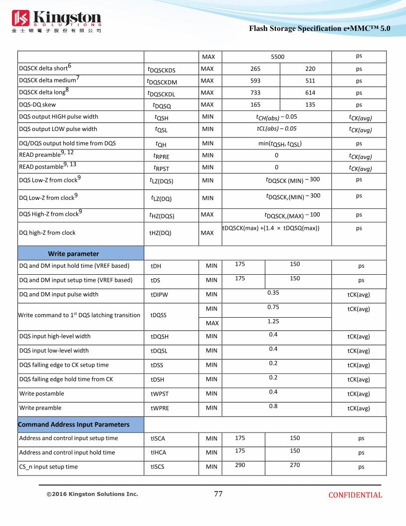
____________________________________________________________________________________________________________________
CONFIDENTIAL
77 © 2016 Kingston Solutions Inc.
Flash Storage Specification e•MMC™ 5.0
Flash Storage Specification
e•MMC™ 4.5
Flash Storage Specification
e•MMC™ 4.5
MAX 5500 ps
DQSCK delta short6 tDQSCKDS MAX 265 220 ps
DQSCK delta medium7 tDQSCKDM MAX 593 511 ps
DQSCK delta long8 tDQSCKDL MAX 733 614 ps
DQS-DQ skew tDQSQ MAX 165 135 ps
DQS output HIGH pulse width tQSH MIN tCH(abs) – 0.05 tCK(avg)
DQS output LOW pulse width tQSL MIN tCL(abs) – 0.05 tCK(avg)
DQ/DQS output hold time from DQS tQH MIN min(tQSH, tQSL) ps
READ preamble9, 12 tRPRE MIN 0.9
tCK(avg)
READ postamble9, 13 tRPST MIN 0.3
tCK(avg)
DQS Low-Z from clock9 tLZ(DQS) MIN tDQSCK (MIN) – 300 ps
DQ Low-Z from clock9 tLZ(DQ) MIN tDQSCK,(MIN) – 300 ps
DQS High-Z from clock9 tHZ(DQS) MAX tDQSCK,(MAX) – 100 ps
DQ high-Z from clock tHZ(DQ) MAX tDQSCK(max) +(1.4 × tDQSQ(max)) ps
Write parameter
DQ and DM input hold time (VREF based) tDH MIN 175 150 ps
DQ and DM input setup time (VREF based) tDS MIN 175 150 ps
DQ and DM input pulse width tDIPW MIN 0.35 tCK(avg)
Write command to 1st DQS latching transition tDQSS MIN 0.75 tCK(avg)
MAX 1.25
DQS input high-level width tDQSH MIN 0.4 tCK(avg)
DQS input low-level width tDQSL MIN 0.4 tCK(avg)
DQS falling edge to CK setup time tDSS MIN 0.2 tCK(avg)
DQS falling edge hold time from CK tDSH MIN 0.2 tCK(avg)
Write postamble tWPST MIN 0.4 tCK(avg)
Write preamble tWPRE MIN 0.8 tCK(avg)
Command Address Input Parameters
Address and control input setup time tISCA MIN 175 150 ps
Address and control input hold time tIHCA MIN 175 150 ps
CS_n input setup time tISCS MIN 290 270 ps

____________________________________________________________________________________________________________________
CONFIDENTIAL
78 © 2016 Kingston Solutions Inc.
Flash Storage Specification e•MMC™ 5.0
Flash Storage Specification
e•MMC™ 4.5
Flash Storage Specification
e•MMC™ 4.5
CS_n input hold time tIHCS MIN 290 270 ps
Address and control input pulse width tIPWCA MIN 0.35 tCK(avg) tCK(avg)
CS_n input pulse width tIPWCS MIN 0.7 tCK(avg) tCK(avg)
CKE Input Parameters
CKE min. pulse width (high and low pulse width) tCKE
tCKE MIN 0.75 ns
CKE input setup time tISCKE*1 MIN 0.25 tCK(avg)
CKE input hold time tIHCKE*2 MIN 0.25 tCK(avg)
Command path disable delay tCPDED MIN 2 tCK(avg)
Boot Parameters (10 MHz – 55 MHz)
Clock cycle time tCKb MAX 100 ns
MIN 18
CKE input setup time tISCKEb MIN 2.5 ns
CKE input hold time tIHCKEb MIN 2.5 ns
Address & control input setup time tISb MIN 1150 ps
Address & control input hold time tIHb MIN 1150 ps
DQS output data access time from CK_t, CK_c tDQSCKb MIN 2.0 ns
MAX 10
Data strobe edge to output data edge tDQSQb MAX 1.2 ns
Mode Register Parameters
MODE REGISTER WRITE command
period tMRW MIN 10 tCK(avg)
Mode register set command delay (MRW command to non-MRW command interval) tMRD MIN 14 ns
MODE REGISTER READ command period tMRR MIN 4 tCK(avg)
Additional time after tXP has expired until MRR command may be issued
tMRRI MIN tRCD (MIN) ns
Core Parameters20
READ latency RL MIN 10 12 tCK(avg)
WRITE latency (set A) WL MIN 6 6 tCK(avg)
WRITE latency (set B) WL MIN 8 9 tCK(avg)

____________________________________________________________________________________________________________________
CONFIDENTIAL
79 © 2016 Kingston Solutions Inc.
Flash Storage Specification e•MMC™ 5.0
Flash Storage Specification
e•MMC™ 4.5
Flash Storage Specification
e•MMC™ 4.5
ACTIVATE-to- ACTIVATE command period tRC MIN
tRAS + tRPab
(with all/pre-bank precharge)
ns
CKE minimum pulse width during SELF REFRESH (low pulse width during SELF REFRESH)
tCKESR MIN 15 ns
SELF REFRESH exit to next valid com- mand delay
tXSR MIN tRFCab + 10 ns
Exit power- down to next valid command delay
tXP MIN 7.5 ns
CAS-to-CAS delay tCCD MIN 4 tCK(avg)
Internal READ to PRECHARGE com- mand delay
tRTP MIN 7.5 ns
RAS-to-CAS delay tRCD (typ) MIN 18 ns
Row precharge time (single bank)
tRPpb (typ) MIN 18 ns
Row precharge time(all banks)
tRPpab (typ) MIN 21 ns
Row active time tRAS MIN 42 ns
MAX 70 µs
WRITE recovery time tWR MIN 15 ns
Internal WRITE-to- READ command delay tWTR MIN 7.5 ns
Active bank A to active bank B tRRD MIN 10 ns
Four-bank ACTIVATE window tFAW MIN 50 ns
Minimum deep power- down time tDPD MIN 500 µs
ODT Parameters
Asynchronous RTT turn-on dely from ODT input
tODTon MIN 1.75 ns
MAX 3.5
Asynchronous RTT turn-off delay from ODT input
tODToff MIN 1.75 ns
MAX 3.5
Automatic RTT turn-on delay after READ data
tAODTon MAX tDQSCK + 1.4 × tDQSQ,max + tCK(avg,min)
ps
Automatic RTT turn-off delay after READ data
tAODToff MIN tDQSCK,min – 300 ps
RTT disable delay from power down, self- refresh, and deep power down entry
tODTd MAX 12 ns
RTT enable delay from power down and self refresh exit
tODTe MAX 12 ns

____________________________________________________________________________________________________________________
CONFIDENTIAL
80 © 2016 Kingston Solutions Inc.
Flash Storage Specification e•MMC™ 5.0
Flash Storage Specification
e•MMC™ 4.5
Flash Storage Specification
e•MMC™ 4.5
CA Training Parameters
First CA calibration command after CA
calibration mode is programmed
tCAMRD MIN 20 tCK(avg)
First CA calibration command after CKE
is LOW
tCAENT MIN 10 tCK(avg)
CA 80alibration exit command after CKE is HIGH
tCAEXT MIN 10 tCK(avg)
CKE LOW after CA calibration mode is
programmed
tCACKEL MIN 10 tCK(avg)
CKE HIGH after the last CA calibration
results are driven.
tCACKEH MIN 10 tCK(avg)
Data out delay after CA training calibra-
tion command is programmed
tADR MAX 20 ns
MRW CA exit command to DQ tri-state tMRZ MIN 3 ns
CA calibration command to CA calibration command delay
tCACD MIN RU (tADR/tCK) + 2 tCK(avg)
Write Leveling Parameters
DQS_t/DQS_c delay after write leveling mode is programmed
tWLDQSN MIN 25 ns
MAX --
First DQS_t/DQS_c edge after write level- ing mode is programmed
tWLMRD MIN 40 ns
MAX --
Write leveling output delay tWLO MIN 0 ns
MAX 20
Write leveling hold time tWLH MIN 205 175 ps
Write leveling setup time tWLS MIN 205 175 ps
Mode register set command delay tMRD MIN max(14ns, 10nCK ) ns
MAX --

____________________________________________________________________________________________________________________
CONFIDENTIAL
81 © 2016 Kingston Solutions Inc.
Flash Storage Specification e•MMC™ 5.0
Flash Storage Specification
e•MMC™ 4.5
Flash Storage Specification
e•MMC™ 4.5
Notes: 1. Frequency values are for reference only. Clock cycle time (tCK) is used to determine device capabilities
2. All AC timings assume an input slew rate of 2 V/ns for single ended signals 3. Measured with 4 V/ns differential CK_t/CK_c slew rate and nominal VIX. 4. All timing and voltage measurements are defined ‘at the ball’, 5. READ, WRITE, and input setup and hold values are referenced to VREF. 6. tDQSCKDS is the absolute value of the difference between any two tDQSCK measurements (in a byte lane) within a
contig- uous sequence of bursts in a 160ns rolling window. tDQSCKDS is not tested and is guaranteed by design. Temperature drift in the system is < 10 °C/s. Values do not include clock jitter..
7. tDQSCKDM is the absolute value of the difference between any two tDQSCK measurements (in a byte lane) within a 1.6µs rolling window. tDQSCKDM is not tested and is guaranteed by design. Temperature drift in the system is < 10 °C/s. Values do not include clock jitter
8. tDQSCKDL is the absolute value of the difference between any two tDQSCK measurements (in a byte lane) within a 32ms rolling window. tDQSCKDL is not tested and is guaranteed by design. Temperature drift in the system is < 10 °C/s. Values do not include clock jitter.
9. For LOW-to-HIGH and HIGH-to-LOW transitions, the timing reference is at the point when the signal crosses the tran- sition threshold (VTT). tHZ and tLZ transitions occur in the same access time (with respect to clock) as valid data transitions. These parameters are not referenced to a specific voltage level but to the time when the device output is no longer driving (for tRPST, tHZ(DQS) and tHZ(DQ)), or begins driving (for tRPRE, tLZ(DQS), tLZ(DQ)). Figure 34 shows a method to calculate the point when device is no longer driving tHZ(DQS) and tHZ(DQ), or begins driving tLZ(DQS), tLZ(DQ) by measuring the signal at two different volt- ages. The actual voltage measurement points are not critical as long as the calculation is consistent.
10. Output Transition Timing.
Figure 34 — tLZ and tHZ Method for Calculating Transition and Endpoints
The parameters tLZ(DQS), tLZ(DQ), tHZ(DQS), and tHZ(DQ) are defined as single-ended. The timing parameters tRPRE and tRPST are determined from the differential signal DQS-/DQS.
11. The parameters tLZ(DQS), tLZ(DQ), tHZ(DQS), and tHZ(DQ) are defined as single-ended. The timing parameters tRPRE and tRPST are determined from the differential signal DQS/DQS#.
12. Measured from the point when DQS_t/DQS_c begins driving the signal to the point when DQS_t/DQS_c begins driv- ing the first rising strobe edge.
13. Measured from the last falling strobe edge of DQS_t/DQS_c to the point when DQS_t/DQS_c finishes driving the signal.
14. CKE input setup time is measured from CKE reaching a HIGH/LOW voltage level to CK_t/CK_c crossing. 15. CKE input hold time is measured from CK_t/CK_c crossing to CKE reaching a HIGH/LOW voltage level. 16. Input set-up/hold time for signal (CA[9:0], CS_n). 17. To ensure device operation before the device is configured, a number of AC boot-timing parameters are defined in
this table. Boot parameter symbols have the letter b appended (for example, tCK during boot is tCKb). 18. The LPDDR3 device will set some mode register default values upon receiving a RESET (MRW) command as speci-
fied in “Mode Register Definition”. 19. The output skew parameters are measured with default output impedance settings using the reference load. 20. The minimum tCK column applies only when tCK is greater than 6ns.

____________________________________________________________________________________________________________________
CONFIDENTIAL
82 © 2016 Kingston Solutions Inc.
Flash Storage Specification e•MMC™ 5.0
Flash Storage Specification
e•MMC™ 4.5
Flash Storage Specification
e•MMC™ 4.5 7.2.11 CA and CS_n Setup, Hold and Derating
For all input signals (CA and CS_n) the total tIS (setup time) and tIH (hold time) required is calculated by adding the data sheet tIS(base) and tIH(base) value to the ΔtIS and ΔtIH derating value respectively. Example: tIS (total setup time) = tIS(base) + ΔtIS.
Setup (tIS) nominal slew rate for a rising signal is defined as the slew rate between the last crossing of VREF(dc) and the first crossing of VIH(ac)min. Setup (tIS) nominal slew rate for a falling signal is defined as the slew rate between the last crossing of VREF(dc) and the first crossing of Vil(ac)max. If the actual signal is always earlier than the nominal slew rate line between shaded ‘VREF(dc) to ac region’, use nominal slew rate for derating value. If the actual signal is later than the nominal slew rate line anywhere between shaded ‘VREF(dc) to ac region’, the slew rate of a tangent line to the actual signal from the ac level to dc level is used for derating value.
Hold (tIH) nominal slew rate for a rising signal is defined as the slew rate between the last crossing of VIL(dc)max and the first crossing of VREF(dc). Hold (tIH) nominal slew rate for a falling signal is defined as the slew rate between the last crossing of VIH(dc)min and the first crossing of VREF(dc). If the actual signal is always later than the nominal slew rate line between shaded ‘dc to VREF(dc) region’, use nominal slew rate for derating value . If the actual signal is earlier than the nominal slew rate line anywhere between shaded ‘dc to VREF(dc) region’, the slew rate of a tangent line to the actual signal from the dc level to VREF(dc) level is used for derating value.
For a valid transition the input signal has to remain above/below VIH/IL(ac) for some time tVAC. Although for slow slew rates the total setup time might be negative (i.e. a valid input signal will not have reached
VIH/IL(ac) at the time of the rising clock transition) a valid input signal is still required to complete the transition and reach VIH/IL(ac).
The derating values may obtained by linear interpolation. These values are typically not subject to production test. They are verified by design and characterization
Table 67 — CA Setup and Hold Base-Values
unit [ps] Data Rate
reference
1333 1600 tISCA(base) 100 75 VIH/L(ac) = VREF(dc) +/-150mV
tISCA(base) - - VIH/L(ac) = VREF(dc) +/-135mV
tIHCA(base) 125 100 VIH/L(dc) = VREF(dc) +/-100mV
NOTE 1 ac/dc referenced for 2V/ns CA slew rate and 4V/ns differential CK_t/CK_c slew rate
Table 68 — CA Setup and Hold Base-Values
unit [ps] Data Rate
reference
1333 1600 tISCS(base) 215 195 VIH/L(ac) = VREF(dc) +/-150mV
tISCS(base) - - VIH/L(ac) = VREF(dc) +/-135mV
tIHCS(base) 240 220 VIH/L(dc) = VREF(dc) +/-100mV

____________________________________________________________________________________________________________________
CONFIDENTIAL
83 © 2016 Kingston Solutions Inc.
Flash Storage Specification e•MMC™ 5.0
Flash Storage Specification
e•MMC™ 4.5
Flash Storage Specification
e•MMC™ 4.5 7.2.11.1 HSUL_12 Driver Output Timing Reference Load
These ‘Timing Reference Loads’ are not intended as a precise representation of any particular system environment or a depiction of the actual load presented by a production tester. System designers should use IBIS or other simulation tools to correlate the timing reference load to a system environment. Manufacturers correlate to their production test conditions, generally one or more coaxial transmission lines terminated at the tester electronics.
Figure 35 — HSUL_12 Driver Output Reference Load for Timing and Slew Rate Note: 1. All output timing parameter values (like tDQSCK, tDQSQ, tQHS, tHZ, tRPRE etc) are reported with respect to this reference load. This reference load is also used to report slew rate.

____________________________________________________________________________________________________________________
CONFIDENTIAL
84 © 2016 Kingston Solutions Inc.
Flash Storage Specification e•MMC™ 5.0
Flash Storage Specification
e•MMC™ 4.5
Flash Storage Specification
e•MMC™ 4.5 Power-up, initialization and Power-Off
DDR3 Mobile RAM Devices must be powered up and initialized in a predefined manner. Operational procedures other than those specified may result in undefined operation.
7.2.12 Power Ramp and Device Initialization
The following sequence must be used to power up the device. Unless specified otherwise, this procedure is mandatory. 1. Power Ramp
While applying power (after Ta), CKE must be held LOW (≤ 0.2 × VDDCA) and all other inputs must be between VILmin and VIHmax. The device outputs remain at High-Z while CKE is held LOW.
Following the completion of the voltage ramp (Tb), CKE must be maintained LOW. DQ, DM, DQS_t and DQS_c voltage levels must be between VSSQ and VDDQ during voltage ramp to avoid latchup. CK_t, CK_c, CS_n, and CA input levels must be between VSSCA and VDDCA during voltage ramp to avoid latch-up. Voltage ramp power supply requirements are provided in Table 69
Table 69 — Voltage Ramp Conditions
After...
Applicable Conditions
Ta is reached
VDD1 must be greater than VDD2—200mV
VDD1 and VDD2 must be greater than VDDCA—200mV
VDD1 and VDD2 must be greater than VDDQ—200mV
Vref must always be less than all other supply voltages
NOTE 1 Ta is the point when any power supply first reaches 300mV. 2 Noted conditions apply between Ta and power-off (controlled or uncontrolled). 3 Tb is the point at which all supply and reference voltages are within their defined operating
ranges 4 Power ramp duration tINIT0 (Tb – Ta) must not exceed 20ms. 5 The voltage difference between any of VSS, VSSQ, and VSSCA pins must not exceed 100mV.
2. CKE and Clock
Beginning at Tb, CKE must remain LOW for at least tINIT1, after which CKE can be asserted HIGH. The clock must be stable at least tINIT2 prior to the first CKE LOW-to-HIGH transition (Tc). CKE, CS_n, and CA inputs must observe setup and hold requirements (tIS, tIH) with respect to the first rising clock edge (as well as to subsequent falling and rising edges). If any MRR commands are issued, the clock period must be within the range defined for tCKb. MRW commands can be issued at normal clock frequencies as long as all AC timings are met. Some AC parameters (for example, tDQSCK) could have relaxed timings (such as tDQSCKb)

____________________________________________________________________________________________________________________
CONFIDENTIAL
85 © 2016 Kingston Solutions Inc.
Flash Storage Specification e•MMC™ 5.0
Flash Storage Specification
e•MMC™ 4.5
Flash Storage Specification
e•MMC™ 4.5 before the system is appropriately configured. While keeping CKE HIGH, NOP commands must be issued for at least tINIT3 (Td). The ODT input signal may be in undefined state until tIS before CKE is registered HIGH. When CKE is registered HIGH, the ODT input signal shall be statically held at either LOW or HIGH. The ODT input signal remains static until the power up initialization sequence is finished, including the expiration of tZQINIT. 3. Reset Command
After tINIT3 is satisfied, the MRW RESET command must be issued (Td). An optional PRECHARGE ALL command can be issued prior to the MRW RESET command. Wait at least tINIT4 while keeping CKE asserted and issuing NOP commands. Only NOP commands are allowed during time tINIT4. 4. Mode Registers Reads and Device Auto-Initialization (DAI) polling:
After tINIT4 is satisfied (Te), only MRR commands and power-down entry/exit commands are supported. After Te, CKE can go LOW in alignment with power-down entry and exit specifications. MRR commands are only valid at this time if the CA bus does not need to be trained. CA Training may only begin after time Tf. User may issue MRR command to poll the DAI bit which will indicate if device auto initialization is complete; once DAI bit indicates completion, SDRAM is in idle state. Device will also be in idle state after tINIT5(max) has expired (whether or not DAI bit has been read by MRR command).As the memory output buffers are not properly configured by Te, some AC parameters must have relaxed timings before the system is appropriately configured. After the DAI bit (MR0, DAI) is set to zero by the memory device (DAI complete), the device is in the idle state (Tf). DAI status can be determined by issuing the MRR command to MR0. The device sets the DAI bit no later than tINIT5 after the RESET command. The controller must wait at least tINIT5(max) or until the DAI bit is set before proceeding. 5. ZQ Calibration:
If CA Training is not required, the MRW initialization calibration (ZQ_CAL) command can be issued to the memory (MR10) after time Tf. If CA Training is required, the CA Training may begin at time Tf. See 4.11.3, Mode Register Write – CA Training Mode for the CA Training command. No other CA commands (other than RESET or NOP) may be issued prior to the completion of CA Training. At the completion of CA Training (Tf’), the MRW initialization calibration (ZQ_CAL) command can be issued to the memory (MR10). This command is used to calibrate output impedance over process, voltage, and temperature. In systems where more than one LPDDR3 device exists on the same bus, the controller must not overlap MRW ZQ_CAL commands. The device is ready for normal operation after tZQINIT.. 6. Normal Operation:
After tZQINIT (Tg), MRW commands must be used to properly configure the memory (for example the output buffer drive strength, latencies, etc.). Specifically, MR1, MR2, and MR3 must be set to configure the memory for the target frequency and memory configuration. After the initialization sequence is complete, the device is ready for any valid command. After Tg,
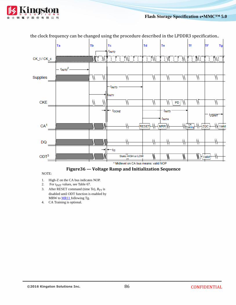
____________________________________________________________________________________________________________________
CONFIDENTIAL
86 © 2016 Kingston Solutions Inc.
Flash Storage Specification e•MMC™ 5.0
Flash Storage Specification
e•MMC™ 4.5
Flash Storage Specification
e•MMC™ 4.5 the clock frequency can be changed using the procedure described in the LPDDR3 specification..
Figure36 — Voltage Ramp and Initialization Sequence
NOTE:
1. High-Z on the CA bus indicates NOP.
2. For tINIT values, see Table 67.
3. After RESET command (time Te), RTT is
disabled until ODT function is enabled by
MRW to MR11 following Tg.
4. CA Training is optional.

____________________________________________________________________________________________________________________
CONFIDENTIAL
87 © 2016 Kingston Solutions Inc.
Flash Storage Specification e•MMC™ 5.0
Flash Storage Specification
e•MMC™ 4.5
Flash Storage Specification
e•MMC™ 4.5 Table 70 Timing Parameters for Initialization
Symbol min. max. Unit Comment
tINIT0 — 20 ms Maximum Power Ramp Time
tINIT1 100 — ns Minimum CKE low time after completion of power ramp
tINIT2 5 — tCK Minimum stable clock before first CKE high
tINIT3 200 — μs Minimum Idle time after first CKE assertion
tINIT4 1 — μs Minimum Idle time after Reset command
tINIT5 — 10 μs Maximum duration of Device Auto-Initialization
tZQINIT 1 — μs ZQ Initial Calibration
tCKb 18 100 ns Clock cycle time during boot
NOTE 1 If DAI bit is not read via MRR, SDRAM will be in idle state after tINIT5(max) has expired
7.2.13 Initialization After Reset (without Power Ramp):
If the RESET command is issued before or after the power-up initialization sequence, the re-initialization procedure must begin at Td. 7.2.14 Power-Off Sequence
The following procedure is required to power off the device. While powering off, CKE must be held LOW (≤ 0.2 × VDDCA); all other inputs must be between VILmin and VIHmax. The device outputs remain at High-Z while CKE is held LOW. DQ, DM, DQS_t, and DQS_c voltage levels must be between VSSQ and VDDQ during the power-off sequence to avoid latch-up. CK_t, CK_c, CS_n, and CA input levels must be between VSSCA and VDDCA during the power-off sequence to avoid latch-up. Tx is the point where any power supply drops below the minimum value specified. Tz is the point where all power supplies are below 300mV. After Tz, the device is powered off. The voltage difference between any of VSS, VSSQ, and VSSCA pins must not exceed 100mV
Table 71 Power supply conditions
Between...
Applicable Conditions
Tx and Tz VDD1 must be greater than VDD2—200mV
Tx and Tz VDD1 must be greater than VDDCA—200mV
Tx and Tz VDD1 must be greater than VDDQ—200mV
Tx and Tz VREF must always be less than all other supply voltages

____________________________________________________________________________________________________________________
CONFIDENTIAL
88 © 2016 Kingston Solutions Inc.
Flash Storage Specification e•MMC™ 5.0
Flash Storage Specification
e•MMC™ 4.5
Flash Storage Specification
e•MMC™ 4.5 7.2.15 Uncontrolled Power-Off Sequence
When an uncontrolled power-off occurs, the following conditions must be met:
At Tx, when the power supply drops below the minimum values specified, all power supplies must be turned off and all power-supply current capacity must be at zero, except for any static charge remaining in the system.
After Tz (the point at which all power supplies first reach 300mV), the device must power off. During this period, the relative voltage between power supplies is uncontrolled. VDD1 and VDD2 must decrease with a slope lower than 0.5 V/µs between Tx and Tz.
An uncontrolled power-off sequence can occur a maximum of 400 times over the life of the device
Table 72 — Timing Parameters Power-Off
Symbol
Value
Unit
Comment min max
tPOFF - 2 s Maximum Power-Off ramp time

____________________________________________________________________________________________________________________
CONFIDENTIAL
89 © 2016 Kingston Solutions Inc.
Flash Storage Specification e•MMC™ 5.0
Flash Storage Specification
e•MMC™ 4.5
Flash Storage Specification
e•MMC™ 4.5 7.2.16 Command truth table.
Table 73 Command Truth Table
Operation or timing that is not specified is illegal, and after such an event, in order to guarantee proper operation, the LPDDR3 device must be powered down and then restarted through the specified initialization sequence before normal operation can continue.

____________________________________________________________________________________________________________________
CONFIDENTIAL
90 © 2016 Kingston Solutions Inc.
Flash Storage Specification e•MMC™ 5.0
Flash Storage Specification
e•MMC™ 4.5
Flash Storage Specification
e•MMC™ 4.5
Notes: 1. All LPDDR3 commands are defined by states of CS_n, CA0, CA1, CA2, CA3, and CKE at the rising edge of the clock 2. Bank addresses BA0, BA1, BA2 (BA) determine which bank is to be operated upon. 3. AP “high” during a READ or WRITE command indicates that an auto-precharge will occur to the bank associated with the
READ or WRITE command. 4. X” means “H or L (but a defined logic level)”, except when the LPDDR3 SDRAM is in PD, SREF, or DPD, in which case CS_n,
CK_t/CK_c, and CA can be floated after the required tCPDED time is satisfied, and until the required exit procedure is initiated as described in the respective entry/exit procedure”
5. Self refresh exit and Deep Power Down exit are asynchronous. 6. VREF must be between 0 and VDDQ during Self Refresh and Deep Power Down operation. 7. Caxr refers to command/address bit “x” on the rising edge of clock. 8. Caxf refers to command/address bit “x” on the falling edge of clock. 9. CS_n and CKE are sampled at the rising edge of clock 10. The least-significant column address C0 is not transmitted on the CA bus, and is implied to be zero. 11. AB “high” during Precharge command indicates that all bank Precharge will occur. In this case, Bank Address is do-not-
care. 12. When CS_n is HIGH, LPDDR3 CA bus can be floated

____________________________________________________________________________________________________________________
CONFIDENTIAL
91 © 2016 Kingston Solutions Inc.
Flash Storage Specification e•MMC™ 5.0
Flash Storage Specification
e•MMC™ 4.5
Flash Storage Specification
e•MMC™ 4.5
Device Current State*3 CKEn-1
*4
*4 CS_n*5
*6
Operation n*6 Device Next State Notes
Active
Power Down
L L X X Maintain Active Power Down Active Power Down
L H H NOP Exit Active Power Down Active 7
Idle Power Down
L L X X Maintain Idle Power Down Idle Power Down
L H H NOP Exit Idle Power Down Idle 7
Resetting
Power Down
L
L
X
X
Maintain
Resetting Power Down
Resetting
Power Down
L
H
H
NOP
Exit Resetting Power Down
Idle or
Resetting
7, 10
Deep Power Down
L
L
X
X
Maintain
Deep Power Down
Deep Power Down
L H H NOP Exit Deep Power Down Power On 9
Self Refresh
L L X X Maintain Self Refresh Self Refresh
L H H NOP Exit Self Refresh Idle 8
Bank(s) Active
H
L
H
NOP
Enter
Active Power Down
Active Power Down
All Banks Idle
H
L
H
NOP
Enter
Idle Power Down
Idle Power Down
11
H
L
L
Enter Self-
Refresh
Enter
Self Refresh
Self Refresh
H
L
L
Enter
Deep Power Down
Enter
Deep Power Down
Deep Power Down
Resetting
H
L
H
NOP
Enter
Resetting Power Down
Resetting Power Down
H H Refer to the Command Truth Table
7.2.17 CKE Truth Table
Table 74 — LPDDR3: CKE Table
NOTE
1 All states and sequences not shown are illegal or reserved unless explicitly described elsewhere in this document. 2 ‘X’ means ‘Don’t care’. 3 “Current state” is the state of the LPDDR3 device immediately prior to clock edge n. 4 “CKEn” is the logic state of CKE at clock rising edge n; “CKEn-1” was the state of CKE at the previous clock edge. 5 “CS_n” is the logic state of CS_n at the clock rising edge n; 6 “Command n” is the command registered at clock edge N, and “Operation n” is a result of “Command n”. 7 Power Down exit time (tXP) should elapse before a command other than NOP is issued. The clock must toggle at least twice during the tXP period. 8 Self-Refresh exit time (tXSR) should elapse before a command other than NOP is issued. The clock must toggle at least twice during the tXSR time. 9 The Deep Power-Down exit procedure must be followed as discussed in the Deep Power-Down section of the Func- tional Description. 10 Upon exiting Resetting Power Down, the device will return to the Idle state if tINIT5 has expired. 11 In the case of ODT disabled, all DQ output shall be Hi-Z. In the case of ODT enabled, all DQ shall be terminated to VDDQ.

____________________________________________________________________________________________________________________
CONFIDENTIAL
92 © 2016 Kingston Solutions Inc.
Flash Storage Specification e•MMC™ 5.0
Flash Storage Specification
e•MMC™ 4.5
Flash Storage Specification
e•MMC™ 4.5 7.3 Mode Register Definition
Table 63 shows the mode registers for DDR3 Mobile RAM. Each register is denoted as “R” if it can be read but not written and “W” if it can be written but not read. Mode Register Read command shall be used to read a register. Mode Register Write command shall be used to write a register
Table 75 Mode Register Assignment
Notes: 1. RFU bits shall be set to ‘0’ during Mode Register writes.
2. RFU bits shall be read as ‘0’ during Mode Register reads. 3. All Mode Registers that are specified as RFU or write-only shall return undefined data when read and DQS_t, DQS_c
shall be toggled. 4. All Mode Registers that are specified as RFU shall not be written. 5. Writes to read-only registers shall have no impact on the functionality of the device.

____________________________________________________________________________________________________________________
CONFIDENTIAL
93 © 2016 Kingston Solutions Inc.
Flash Storage Specification e•MMC™ 5.0
Flash Storage Specification
e•MMC™ 4.5
Flash Storage Specification
e•MMC™ 4.5 MR#0_Device Information (MA<7:0> = 00H): Read-only
OP7 OP6 OP5 OP4 OP3 OP2 OP1 OP0
RL3 WL (Set B)
Support
(RFU) RZQI (RFU) DAI
OP<0> DAI (Device Auto-Initialization Status)
0B: DAI complete
1B: DAI still in progress
OP<4:3> RZQI (Built in Self Test for RZQ Information)
01B: ZQ-pin may connect to VDDCA or float
10B: ZQ-pin may short to GND
11B: ZQ-pin self test completed, no error condition detected
(ZQ-pin may not connect to VDDCA or float nor short to GND)
OP<6> WL (Set B) Support
1B: DRAM supports WL (Set B)
OP<7> RL3 Support
1B: DRAM supports
RL = 3, nWR = 3, WL = 1 for frequescies ≤ 166MHz
Notes: 1. RZQI will be set upon completion of the MRW ZQ Initialization Calibration command. 2. If ZQ is connected to VDDCA to set default calibration, OP[4:3] shall be set to 01. If ZQ is not connected to VDDCA, either OP[4:3]=01 or OP[4:3]=10 might indicate a ZQ-pin assembly error. It is recommended that the assembly error is corrected. 3. In the case of possible assembly error (either OP[4:3]=01 or OP[4:3]=10 per Note 2), the DDR3 Mobile RAM device will default to factory trim settings for RON, and will ignore ZQ calibration commands. In either case, the system may not function as intended. 4. In the case of the ZQ self-test returning a value of 11b, this result indicates that the device has detected a resistor connection to the ZQ pin. However, this result cannot be used to validate the ZQ resistor value or that the ZQ resistor tolerance meets the specified limits (i.e. 240Ω ± 1%).
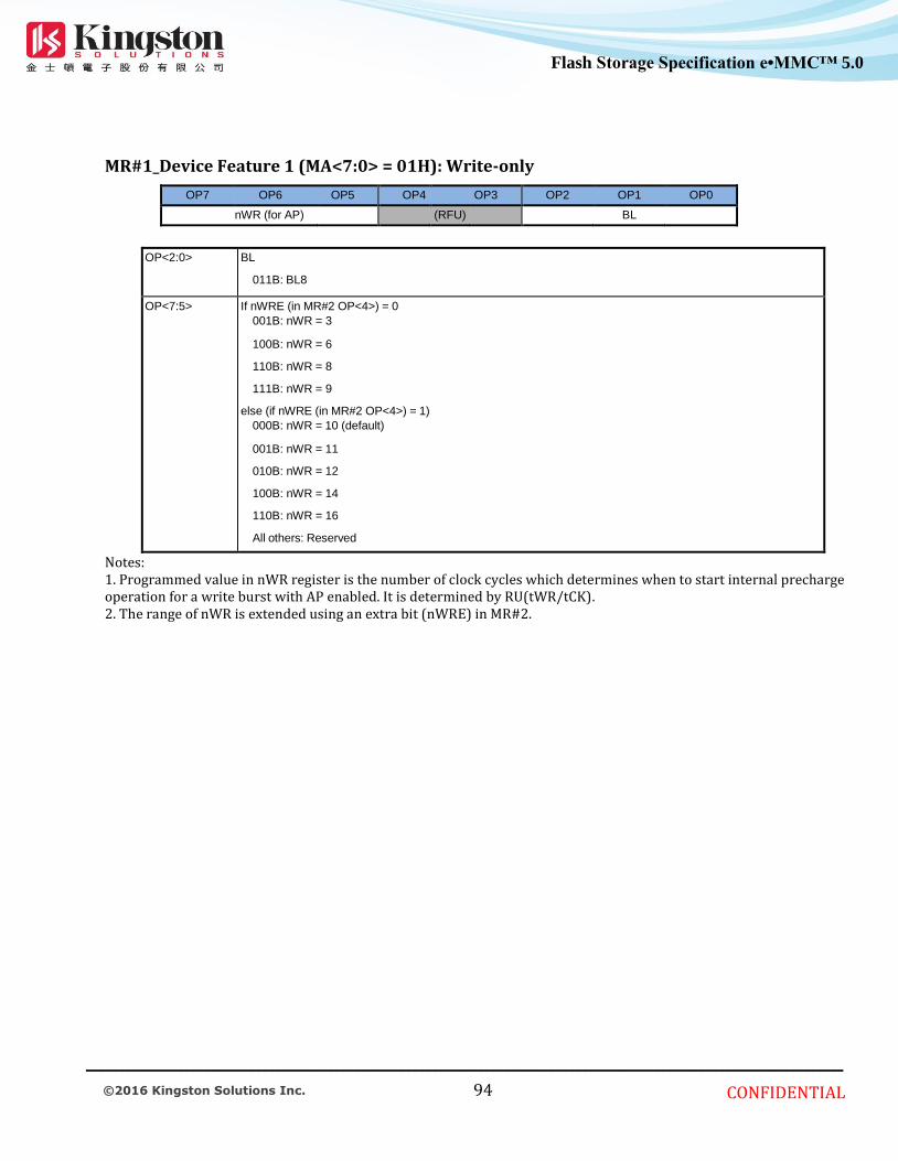
____________________________________________________________________________________________________________________
CONFIDENTIAL
94 © 2016 Kingston Solutions Inc.
Flash Storage Specification e•MMC™ 5.0
Flash Storage Specification
e•MMC™ 4.5
Flash Storage Specification
e•MMC™ 4.5
MR#1_Device Feature 1 (MA<7:0> = 01H): Write-only
OP7 OP6 OP5 OP4 OP3 OP2 OP1 OP0
nWR (for AP) (RFU) BL
OP<2:0> BL
011B: BL8
All others: Reserved OP<7:5> If nWRE (in MR#2 OP<4>) = 0
001B: nWR = 3
100B: nWR = 6
110B: nWR = 8
111B: nWR = 9
else (if nWRE (in MR#2 OP<4>) = 1)
000B: nWR = 10 (default)
001B: nWR = 11
010B: nWR = 12
100B: nWR = 14
110B: nWR = 16
All others: Reserved
Notes: 1. Programmed value in nWR register is the number of clock cycles which determines when to start internal precharge operation for a write burst with AP enabled. It is determined by RU(tWR/tCK). 2. The range of nWR is extended using an extra bit (nWRE) in MR#2.

____________________________________________________________________________________________________________________
CONFIDENTIAL
95
© 2016 Kingston Solutions Inc.
Flash Storage Specification e•MMC™ 5.0
Flash Storage Specification
e•MMC™ 4.5
Flash Storage Specification
e•MMC™ 4.5
MR#2_Device Feature 2 (MA<7:0> = 02H): Write-only
OP7 OP6 OP5 OP4 OP3 OP2 OP1 OP0
Write Leveling
WL Select (RFU) nWRE RL & WL
OP<3:0> RL & WL
If OP<6> = 0 (WL Set A, default)
0001B: RL = 3/ WL = 1 (≤ 166MHz) *1
0100B: RL = 6 / WL = 3 (≤ 400MHz)
0110B: RL = 8 / WL = 4 (≤ 533MHz)
0111B: RL = 9 / WL = 5 (≤ 600MHz)
1000B: RL = 10 / WL = 6 (≤ 667MHz, default)
1001B: RL = 11 / WL = 6 (≤ 733MHz)
1010B: RL = 12 / WL = 6 (≤ 800MHz)
All others: Reserved
If OP<6> = 1(WL Set B *1)
0001B: RL = 3/ WL = 1 (≤ 166MHz) *1
0100B: RL = 6 / WL = 3 (≤ 400MHz)
0110B: RL = 8 / WL = 4 (≤ 533MHz)
0111B: RL = 9 / WL = 5 (≤ 600MHz)
1000B: RL = 10 / WL = 8 (≤ 667MHz, default)
1001B: RL = 11 / WL = 9 (≤ 733MHz)
1010B: RL = 12 / WL = 9 (≤ 800MHz)
All others: Reserved
OP<4> nWRE
0B: Enable nWR programming ≤ 9
1B: Enable nWR programming > 9 (default) OP<6> WL Select
0B: Select WL Set A (default)
1B: Select WL Set B *2
OP<7> Write Leveling
0B: Write Leveling Mode disabled (default)
1B: Write Leveling Mode enabled
Notes: 1. See MR#0, OP<7>
2. See MR#0, OP<6>
Table 9: DDR3 Mobile RAM Read and Write Latency
Data Rate [Mbps] 333 800 1066 1200 1333 1466 1600
tCK [ns] 6 2.5 1.875 1.67 1.5 1.36 1.25
RL 3 6 8 9 10 11 12
WL (Set A) 1 3 4 5 6 6 6
WL (Set B) 1 3 4 5 8 9 9

____________________________________________________________________________________________________________________
CONFIDENTIAL
96 © 2016 Kingston Solutions Inc.
Flash Storage Specification e•MMC™ 5.0
Flash Storage Specification
e•MMC™ 4.5
Flash Storage Specification
e•MMC™ 4.5 MR#3_I/O Configuration 1 (MA<7:0> = 03H): Write-only
OP7 OP6 OP5 OP4 OP3 OP2 OP1 OP0
(RFU) DS
OP<3:0> DS
0001B: 34.3Ω typical pull-down/pull-up
0010B: 40Ω typical pull-down/pull-up (default)
0011B: 48Ω typical pull-down/pull-up
0100B: Reserved
0110B: Reserved
1001B: 34.3Ω typical pull-down, 40Ω typical pull-up
1010B: 40Ω typical pull-down, 48Ω typical pull-up
1011B: 34.3Ω typical pull-down, 48Ω typical pull-up
All others: Reserved

____________________________________________________________________________________________________________________
CONFIDENTIAL
97 © 2016 Kingston Solutions Inc.
Flash Storage Specification e•MMC™ 5.0
Flash Storage Specification
e•MMC™ 4.5
Flash Storage Specification
e•MMC™ 4.5 MR#4_Device Temperature (MA<7:0> = 04H): Read-only
OP7 OP6 OP5 OP4 OP3 OP2 OP1 OP0
TUF (RFU) Refresh Rate
OP<2:0> Refresh Rate
000B: Low temperature operating limit exceeded
001B: 4 × tREFI, 4 × tREFIpb, 4 × tREFW
010B: 2 × tREFI, 2 × tREFIpb, 2 × tREFW
011B: 1 × tREFI, 1 × tREFIpb, 1 × tREFW(≤ +85°C)
100B: 0.5 × tREFI, 0.5 × tREFIpb, 0.5 × tREFW
101B: 0.25 × tREFI, 0.25 × tREFIpb, 0.25 × tREFW, do not de-rate AC timing
110B: 0.25 × tREFI, 0.25 × tREFIpb, 0.25 × tREFW, de-rate AC timing
111B: High temperature operating limit exceeded
OP<7> TUF(Temperature Update Flag) 0B: OP<2:0> value has not changed since last read of MR4. 1B: OP<2:0> value has changed since last read of MR4.
Notes: 1. A Mode Register Read from MR4 will reset OP7 to ‘0’. 2. OP7 is reset to ‘0’ at power-up. OP<2:0> bits are undefined after power-up. 3. If OP2 equals ‘1’, the device temperature is greater than 85°C. 4. OP7 is set to “1” if OP2:OP0 has changed at any time since the last read of MR4. 5. DDR2 Mobile RAM will drive OP<6:5> to ‘0’. 6. Specified operating temperature range and maximum operating temperature are refer to Section 1 Electrical Conditions on page 6. If maximum temperature is 85°C, functionality for over 85°C is not guaranteed.
MR#5_Basic Configuration 1 (MA<7:0> = 05H): Read-only
OP7 OP6 OP5 OP4 OP3 OP2 OP1 OP0
Manufacturer ID
OP<7:0> Manufacturer ID
00000101B (Nanya)

____________________________________________________________________________________________________________________
CONFIDENTIAL
98 © 2016 Kingston Solutions Inc.
Flash Storage Specification e•MMC™ 5.0
Flash Storage Specification
e•MMC™ 4.5
Flash Storage Specification
e•MMC™ 4.5 MR#8_Basic Configuration 4 (MA<7:0> = 08BH): Read-only
OP7 OP6 OP5 OP4 OP3 OP2 OP1 OP0
I/O width Density Type
OP<1:0> Type
11B: S8 Device
OP<5:2> Density 0110B: 4Gb 0111B: 8Gb
OP<7:6> I/O width 00B: ×32 01B: ×16
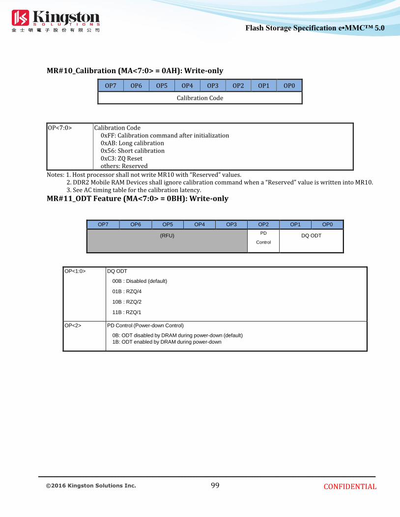
____________________________________________________________________________________________________________________
CONFIDENTIAL
99 © 2016 Kingston Solutions Inc.
Flash Storage Specification e•MMC™ 5.0
Flash Storage Specification
e•MMC™ 4.5
Flash Storage Specification
e•MMC™ 4.5
MR#10_Calibration (MA<7:0> = 0AH): Write-only
OP7 OP6 OP5 OP4 OP3 OP2 OP1 OP0
Calibration Code
OP<7:0> Calibration Code
0xFF: Calibration command after initialization 0xAB: Long calibration 0x56: Short calibration 0xC3: ZQ Reset others: Reserved
Notes: 1. Host processor shall not write MR10 with “Reserved” values. 2. DDR2 Mobile RAM Devices shall ignore calibration command when a “Reserved” value is written into MR10. 3. See AC timing table for the calibration latency.
MR#11_ODT Feature (MA<7:0> = 0BH): Write-only
OP7 OP6 OP5 OP4 OP3 OP2 OP1 OP0
(RFU) PD
Control
DQ ODT
OP<1:0> DQ ODT
00B : Disabled (default)
01B : RZQ/4
10B : RZQ/2
11B : RZQ/1
OP<2> PD Control (Power-down Control)
0B: ODT disabled by DRAM during power-down (default)
1B: ODT enabled by DRAM during power-down

____________________________________________________________________________________________________________________
CONFIDENTIAL
100 © 2016 Kingston Solutions Inc.
Flash Storage Specification e•MMC™ 5.0
Flash Storage Specification
e•MMC™ 4.5
Flash Storage Specification
e•MMC™ 4.5 MR#16_PASR_Bank Mask (MA<7:0> = 010H): Write-only
OP7 OP6 OP5 OP4 OP3 OP2 OP1 OP0
Bank Mask
OP<7:0> Bank Mask
0B: refresh enable to the bank (=unmasked, default) 1B: refresh blocked (=masked)
Bank and OP corresponding table
OP<7:0> Bank
Bank # Bank Address
OP0 Bank 0 000B
OP1 Bank 1 001B OP2 Bank 2 010B OP3 Bank 3 011B OP4 Bank 4 100B
OP5 Bank 5 101B
OP6 Bank 6 110B OP7 Bank 7 111B
Note: 1. Each bank can be masked independently by setting each OP value.
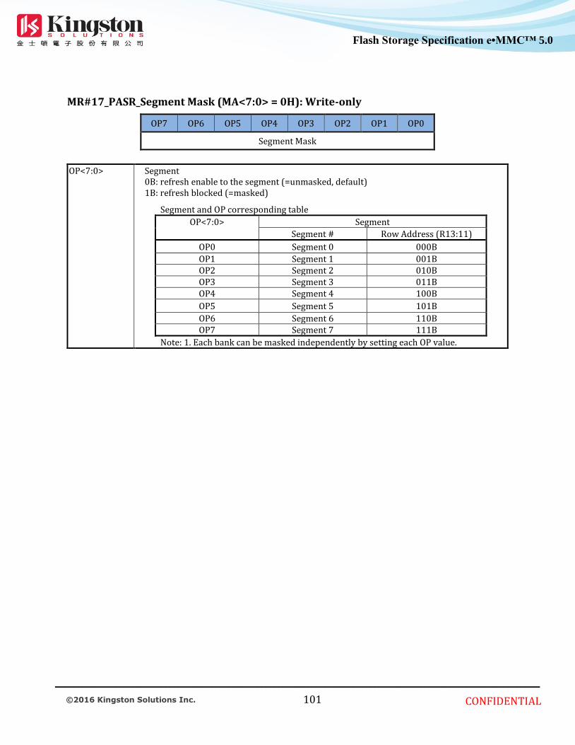
____________________________________________________________________________________________________________________
CONFIDENTIAL
101 © 2016 Kingston Solutions Inc.
Flash Storage Specification e•MMC™ 5.0
Flash Storage Specification
e•MMC™ 4.5
Flash Storage Specification
e•MMC™ 4.5
MR#17_PASR_Segment Mask (MA<7:0> = 0H): Write-only
OP7 OP6 OP5 OP4 OP3 OP2 OP1 OP0
Segment Mask
OP<7:0> Segment
0B: refresh enable to the segment (=unmasked, default) 1B: refresh blocked (=masked)
Segment and OP corresponding table
OP<7:0> Segment
Segment # Row Address (R13:11)
OP0 Segment 0 000B
OP1 Segment 1 001B OP2 Segment 2 010B OP3 Segment 3 011B OP4 Segment 4 100B
OP5 Segment 5 101B
OP6 Segment 6 110B OP7 Segment 7 111B
Note: 1. Each bank can be masked independently by setting each OP value.
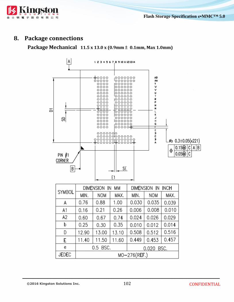
____________________________________________________________________________________________________________________
CONFIDENTIAL
102 © 2016 Kingston Solutions Inc.
Flash Storage Specification e•MMC™ 5.0
Flash Storage Specification
e•MMC™ 4.5
Flash Storage Specification
e•MMC™ 4.5 8. Package connections
Package Mechanical 11.5 x 13.0 x (0.9mm ± 0.1mm, Max 1.0mm)

____________________________________________________________________________________________________________________
CONFIDENTIAL
103 © 2016 Kingston Solutions Inc.
Flash Storage Specification e•MMC™ 5.0
Flash Storage Specification
e•MMC™ 4.5
Flash Storage Specification
e•MMC™ 4.5

____________________________________________________________________________________________________________________
CONFIDENTIAL
104 © 2016 Kingston Solutions Inc.
Flash Storage Specification e•MMC™ 5.0
Flash Storage Specification
e•MMC™ 4.5
Flash Storage Specification
e•MMC™ 4.5 9. Ball Assignment (221 ball)
1 2 3 4 5 6 7 8 9 10 11 12 13 14
A DNU NC VSSm VCCQ DAT6 CMD DS VSSm DAT0 DAT5 VDDI VSSm NC DNU A
B NC VSSm VCC DAT7 DAT3 VCCQ VSSm CLK VCCQ DAT1 VSSm VCC VCC NC B
C RST_n VSSm VCC VSSm DAT2 VCCQ VSSm DAT4 VSSm VCCQ VSSm VSSm C
D NC NC NC NC NC VSSm VCC D
E E
F VSS VDD1 VDD1 VDD2 VDD2 VDD1 DQ29 DQ30 DQ31 VSS F
G ZQ0 ZQ1 VSS VDD1 VSS VDDQ DQ26 VSS DQ27 DQ28 G
H CA9 VSS VSS VSS VDDQ DQS3_t VSS DQ24 VDDQ DQ25 H
J CA8 CA7 VSS VDD2 VSS DQS3_c DM3 VDDQ DQ15 VSS J
K VDDCA CA6 VSS VDD2 VSS VSS VDDQ DQ13 VDDQ DQ14 K
L VDD2 CA5 VSS VDD2 VDDQ VDDQ VSS DQ12 VSS DQ11 L
M VREF (CA) VSS VSS VDD2 VSS DQS1_t VDDQ DQ10 VDDQ DQ9 M
N VDDCA CK_c VSS VDD2 VSS DQS1_c DM1 VDDQ DQ8 VSS N
P VSS CK_t VSS VDD2 VDD2 VSS ODT VDD2 VSSVREF
(DQ)P
R CKE1 VSS VSS VDD2 VSS DQS0_c DM0 VDDQ DQ7 VSS R
T CKE0 CS1_n VSS VDD2 VSS DQS0_t VDDQ DQ5 VDDQ DQ6 T
U VDDCA CS0_n VSS VDD2 VDDQ VDDQ VSS DQ3 VSS DQ4 U
V VDDCA CA4 VSS VDD2 VSS VSS VDDQ DQ1 VDDQ DQ2 V
W CA2 CA3 VSS VDD2 VSS DQS2_c DM2 VDDQ DQ0 VSS W
Y CA0 CA1 VSS VSS VDDQ DQS2_t VSS DQ23 VDDQ DQ22 Y
AA DNU VSS VDD1 VSS VDD1 VSS VDDQ DQ21 VSS DQ20 DQ19 DNU AA
AB DNU DNU VDD1 VDD1 VDD2 VDD2 VDD1 DQ18 DQ17 DQ16 DNU DNU AB
1 2 3 4 5 6 7 8 9 10 11 12 13 14
221 ball assignment

____________________________________________________________________________________________________________________
CONFIDENTIAL
105 © 2016 Kingston Solutions Inc.
Flash Storage Specification e•MMC™ 5.0
Flash Storage Specification
e•MMC™ 4.5
Flash Storage Specification
e•MMC™ 4.5
10. Temperature
Parameter Rating Unit Note
Operating temperature -25 ~ +85 ℃
Storage temperature -55 ~ +125 ℃
11. Marking
YYWW PPPPPPPP
240xxxx-xxx.xxxxxx
xxxxxxx-xxxx
TAIWAN
Kingston logo 240xxxx-xxx.xxxxxx:Internal control number
YYWW:Date code (YY– Last 2 digital of year, WW- Work week)
PPPPPPPP: Internal control number
xxxxxxx-xxxx Sales P/N 2xxxxxx : Internal control number Country:TAIWAN
2xxxxxx

____________________________________________________________________________________________________________________
CONFIDENTIAL
106 © 2016 Kingston Solutions Inc.
Flash Storage Specification e•MMC™ 5.0
Flash Storage Specification
e•MMC™ 4.5
Flash Storage Specification
e•MMC™ 4.5 12. Revision History Rev. History Date Remark Editor 1.0 Preliminary Feb. / 2016

____________________________________________________________________________________________________________________
CONFIDENTIAL
107 © 2016 Kingston Solutions Inc.
Flash Storage Specification e•MMC™ 5.0
Flash Storage Specification
e•MMC™ 4.5
Flash Storage Specification
e•MMC™ 4.5
Appendix

Register Settings:
F/W: 01
Applied Products: 08EMCP04-NL3DT227-A01 / 08EMCP08-NL3DT227-A01
OCR Register Setting:
OCR Register
Definitions OCR bit
VDD voltage window High Voltage
MultimediaCard
Dual voltage
MultimediaCard and e•MMC™
[6:0] Reserved 00 00000b 00 00000b
[7] 1.70 - 1.95V 0b 1b
[14:8] 2.0-2.6V 000 0000b 000 0000b
[23:15] 2.7-3.6V 1 1111 1111b 1 1111 1111b
[28:24] Reserved 0 0000b 0 0000b
[30:29] Access Mode 00b (byte mode)
10b (sector mode)
00b (byte mode)
10b (sector mode)
[31] (Device power up status bit (busy)1
Note1:This bit is set to LOW if the Device has not finished the power up routine.
CID Register Setting:
CID Fields Name Field Width CID slice Value
Manufacturer ID MID 8 [127:120] 70h
Reserved 6 [119:114] 0h
Device/BGA CBX 2 [113:112] 1h
OEM/Application ID OID 8 [111:104] 0h
Product name PNM 48 [103:56] (454838454434h“EH8ED4”)
(454838454538h“EH8EE8”)
Product revision PRV 8 [55:48] 01*
Product serial number PSN 32 [47:16] Random by Production
Manufacturing date MDT 8 [15:8] month, year
CRC7 checksum CRC 7 [7:1] - (Note 1)
not used, always “1” - 1 [0] 1h
Note1:The description are same as e•MMC™ JEDEC standard

CSD Register Setting:
Name Field Width CSD-slice Value
CSD structure CSD_STRUCTURE 2 [127:126] 3h
System specification version SPEC_VERS 4 [125:122] 4h
Reserved - 2 [121:120] 0h
Data read access-time 1 TAAC 8 [119:112] 4Fh
Data read access-time 2 in CLK
cycles (NSAC*100)
NSAC 8 [111:104] 1h
Max. bus clock frequency TRAN_SPEED 8 [103:96] 32h
Device command classes CCC 12 [95:84] F5h
Max. read data block length READ_BL_LEN 4 [83:80] 9h
Partial blocks for read allowed READ_BL_PARTIAL 1 [79:79] 0h
Write block misalignment WRITE_BLK_MISALIGN 1 [78:78] 0h
Read block misalignment READ_BLK_MISALIGN 1 [77:77] 0h
DSR implemented DSR_IMP 1 [76:76] 0h
Reserved - 2 [75:74] 0h
Device size C_SIZE 12 [73:62] FFFh
Max. read current @ VDD min VDD_R_CURR_MIN 3 [61:59] 7h
Max. read current @ VDD max VDD_R_CURR_MAX 3 [58:56] 7h
Max. write current @ VDD min VDD_W_CURR_MIN 3 [55:53] 7h
Max. write current @ VDD max VDD_W_CURR_MAX 3 [52:50] 7h
Device size multiplier C_SIZE_MULT 3 [49:47] 7h
Erase group size ERASE_GRP_SIZE 5 [46:42] 1Fh
Erase group size multiplier ERASE_GRP_MULT 5 [41:37] 1Fh
Write protect group size WP_GRP_SIZE 5 [36:32] 17h
Write protect group enable WP_GRP_ENABLE 1 [31:31] 1h
Manufacturer default ECC DEFAULT_ECC 2 [30:29] 0h
Write speed factor R2W_FACTOR 3 [28:26] 2h
Max. write data block length WRITE_BL_LEN 4 [25:22] 9h
Partial blocks for write allowed WRITE_BL_PARTIAL 1 [21:21] 0h
Reserved - 4 [20:17] 0h
Content protection application CONTENT_PROT_APP 1 [16:16] 0h
File format group FILE_FORMAT_GRP 1 [15:15] 0h
Copy flag (OTP) COPY 1 [14:14] 0h
Permanent write protection PERM_WRITE_PROTECT 1 [13:13] 0h
Temporary write protection TMP_WRITE_PROTECT 1 [12:12] 0h

File format FILE_FORMAT 2 [11:10] 0h
ECC code ECC 2 [9:8] 0h
CRC CRC 7 [7:1] 18h
Not used, always’1’ - 1 [0:0] 1h
Extended CSD Register:
Name Field Size (Bytes) CSD-slice Value
Properties Segment
Reserved1 – 6 [511:506] 0h
Extended Security
Commands Error
EXT_SECURITY_ERR 1 [505] 0h
Supported Command Sets S_CMD_SET 1 [504] 1h
HPI features HPI_FEATURES 1 [503] 1h
Background operations
support
BKOPS_SUPPORT 1 [502] 1h
Max packed read commands MAX_PACKED_READS 1 [501] 3Ch
Max packed write
commands
MAX_PACKED_WRITES 1 [500] 3Ch
Data Tag Support DATA_TAG_SUPPORT 1 [499] 1h
Tag Unit Size TAG_UNIT_SIZE 1 [498] 3h
Tag Resources Size TAG_RES_SIZE 1 [497] 0h
Context management
capabilities
CONTEXT_CAPABILITIES 1 [496] 5h
Large Unit size LARGE_UNIT_SIZE_M1 1 [495] 5h-8GB
Extended partitions
attribute support
EXT_SUPPORT 1 [494] 3h
Supported modes SUPPORTED_MODES 1 [493] 01h
FFU features FFU_FEATURES 1 [492] 0h
Operation codes timeout OPERATION_CODE_TIME_O
UT
1 [491] 0h
FFU Argument FFU_ARG 4 [490:487] 65535
Reserved1 181 [486:306] -
Number of FW sectors
correctly programmed
NUMBER_OF_FW_SECTORS_
CORRECTLY_PROGRAMMED
4 [305:302] 0h
Vendor proprietary health
report
VENDOR_PROPRIETARY_HE
ALTH_REPORT
32 [301:270] 0h
Device life time estimation DEVICE_LIFE_TIME_EST 1 [269] 01h

type B _TYP_B
Device life time estimation
type A
DEVICE_LIFE_TIME_EST_TY
P_A
1 [268] 01h
Pre EOL information PRE_EOL_INFO 1 [267] 01h
Optimal read size OPTIMAL_READ_SIZE 1 [266] 01h
Optimal write size OPTIMAL_WRITE_SIZE 1 [265] 04h
Optimal trim unit size OPTIMAL_TRIM_UNIT_SIZE 1 [264] 01h
Device version DEVICE_VERSION 2 [263:262] 0h
Firmware version FIRMWARE_VERSION 8 [261:254] 01*
Power class for 200MHz,
DDR at VCC=3.6V
PWR_CL_DDR_200_360 1 [253] 0h
Cache size CACHE_SIZE 4 [252:249] 512
Generic CMD6 timeout GENERIC_CMD6_TIME 1 [248] 19h
Power off notification(long)
timeout
POWER_OFF_LONG_TIME 1 [247] FFh
Background operations
status
BKOPS_STATUS 1 [246] 0h
Number of correctly
programmed sectors
CORRECTLY_PRG_SECTORS_
NUM
4 [245:242] 0h
1st initialization time after
partitioning
INI_TIMEOUT_AP 1 [241] 64h
Reserved1 – 1 [240] –
Power class for 52MHz, DDR
at 3.6V
PWR_CL_DDR_52_360 1 [239] 0h
Power class for 52MHz, DDR
at 1.95V
PWR_CL_DDR_52_195 1 [238] 0h
Power class for 200MHz at
3.6V
PWR_CL_200_360 1 [237] 0h
Power class for 200MHz, at
1.95V
PWR_CL_200_195 1 [236] 0h
Minimum Write
Performance for 8bit at
52MHz in DDR mode
MIN_PERF_DDR_W_8_52 1 [235] 0h
Minimum Read Performance
for 8bit at 52MHz in DDR
mode
MIN_PERF_DDR_R_8_52 1 [234] 0h
Reserved1 – 1 [233] –
TRIM Multiplier TRIM_MULT 1 [232] 11h -8GB

Secure Feature support SEC_FEATURE_SUPPORT 1 [231] 55h
Secure Erase Multiplier SEC_ERASE_MULT 1 [230] 1h
Secure TRIM Multiplier SEC_TRIM_MULT 1 [229] 1h
Boot information BOOT_INFO 1 [228] 7h
Reserved1 – 1 [227] –
Boot partition size BOOT_SIZE_MULTI 1 [226] 20h *
Access size ACC_SIZE 1 [225] 6h-8GB
High-capacity erase unit size HC_ERASE_GRP_SIZE 1 [224] 01h-8GB
High-capacity erase timeout ERASE_TIMEOUT_MULT 1 [223] 11h-8GB
Reliable write sector count REL_WR_SEC_C 1 [222] 1h
High-capacity write protect
group size
HC_WP_GRP_SIZE 1 [221] 10h
Sleep current (VCC) S_C_VCC 1 [220] 8h
Sleep current (VCCQ) S_C_VCCQ 1 [219] 8h
Production state awareness
Timeout
PRODUCTION_STATE_AWA
RENESS_TIMEOUT
1 [218] 14h
Sleep/awake timeout S_A_TIMEOUT 1 [217] 12h
Sleep Notification timout SLEEP_NOTIFICATION_TIM
E
1 [216] 0Fh
Sector Count SEC_COUNT 4 [215:212] 00E40000h-8GB*
Reserved (note1) – 1 [211] –
Minimum Write
Performance for 8bit at
52MHz
MIN_PERF_W_8_52 1 [210] 8h
Minimum Read Performance
for 8bit at 52MHz
MIN_PERF_R_8_52 1 [209] 8h
Minimum Write
Performance for 8bit at
26MHz, for 4bit at 52MHz
MIN_PERF_W_8_26_4_52 1 [208] 8h
Minimum Read Performance
for 8bit at 26MHz, for 4bit at
52MHz
MIN_PERF_R_8_26_4_52 1 [207] 8h
Minimum Write
Performance for 4bit at
26MHz
MIN_PERF_W_4_26 1 [206] 8h
Minimum Read Performance
for 4bit at 26MHz
MIN_PERF_R_4_26 1 [205] 8h
Reserved1 – 1 [204] –

Power class for 26MHz at
3.6V 1 R
PWR_CL_26_360 1 [203] 0h
Power class for 52MHz at
3.6V 1 R
PWR_CL_52_360 1 [202] 0h
Power class for 26MHz at
1.95V 1 R
PWR_CL_26_195 1 [201] 0h
Power class for 52MHz at
1.95V 1 R
PWR_CL_52_195 1 [200] 0h
Partition switching timing PARTITION_SWITCH_TIME 1 [199] 3h
Out-of-interrupt busy timing OUT_OF_INTERRUPT_TIME 1 [198] Ah
I/O Driver Strength DRIVER_STRENGTH 1 [197] 1Fh
Device type CARD_TYPE 1 [196] 57h
Reserved (note1) – 1 [195] –
CSD structure version – [194] 2h
Reserved (note1) – 1 [193] –
Extended CSD revision EXT_CSD_REV 1 [192] 07h
Modes Segment
Command set CMD_SET 1 [191] 0h
Reserved (note1) – 1 [190] –
Command set revision CMD_SET_REV 1 [189] 0h
Reserved (note1) – 1 [188] –
Power class POWER_CLASS 1 [187] 0h
Reserved (note1) – 1 [186] –
High-speed interface timing HS_TIMING 1 [185] 1h (note 3)
Reserved (note1) – 1 [184] –
Bus width mode BUS_WIDTH 1 [183] 2h (note 4)
Reserved (note1) – 1 [182] –
Erased memory content ERASED_MEM_CONT 1 [181] 0h
Reserved (note1) – 1 [180] –
Partition configuration PARTITION_CONFIG 1 [179] 0h
Boot config protection BOOT_CONFIG_PROT 1 [178] 0h
Boot bus Conditions BOOT_BUS_CONDITIONS 1 [177] 0h
Reserved (note1) – 1 [176] –
High-density erase group
definition
ERASE_GROUP_DEF 1 [175] 0h
Boot write protection status
registers
BOOT_WP_STATUS 1 [174] 0h

Boot area write protection
register
BOOT_WP 1 [173] 0h
Reserved (note1) – 1 [172] –
User area write protection
register
USER_WP 1 [171] 0h
Reserved (note1) – 1 [170] –
FW configuration FW_CONFIG 1 [169] 0h
RPMB Size RPMB_SIZE_MULT [168] 20h *
Write reliability setting
register
WR_REL_SET [167] 00h
Write reliability parameter
register
WR_REL_PARAM 1 [166] 15h
Start Sanitize operation SANITIZE_START 1 [165] 0h
Manually start background
operations
BKOPS_START 1 [164] 0h
Enable background
operations handshake
BKOPS_EN 1 [163] 0h
H/W reset function RST_n_FUNCTION 1 [162] 0h
HPI management HPI_MGMT 1 [161] 0h
Partitioning Support PARTITIONING_SUPPORT 1 [160] 7h
Max Enhanced Area Size MAX_ENH_SIZE_MULT 3 [159:157] 101
Partitions attribute PARTITIONS_ATTRIBUTE 1 [156] 0h
Partitioning Setting PARTITION_SETTING_
COMPLETED
1 [155] 0h
General Purpose Partition
Size
GP_SIZE_MULT 4 3 [154:152] 0h
General Purpose Partition
Size
GP_SIZE_MULT3 3 [151:149] 0h
General Purpose Partition
Size
GP_SIZE_MULT2 3 [148:146] 0h
General Purpose Partition
Size
GP_SIZE_MULT1 3 [145:143] 0h
Enhanced User Data Area
Size
ENH_SIZE_MULT 3 [142:140] 0h
Enhanced User Data Start
Address
ENH_START_ADDR 4 [139:136] 0h
Reserved (note1) – 1 [135] –
Bad Block Management SEC_BAD_BLK_MGMNT 1 [134] 0h
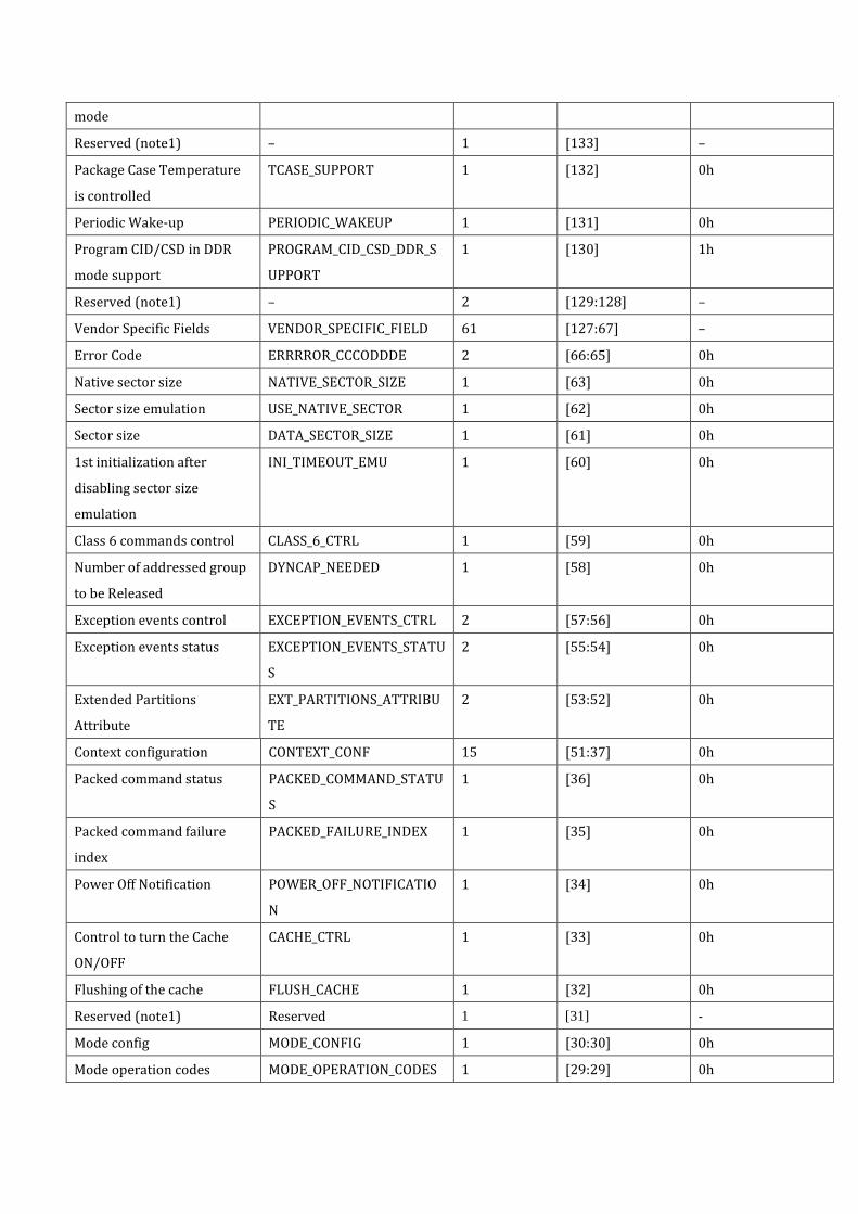
mode
Reserved (note1) – 1 [133] –
Package Case Temperature
is controlled
TCASE_SUPPORT 1 [132] 0h
Periodic Wake-up PERIODIC_WAKEUP 1 [131] 0h
Program CID/CSD in DDR
mode support
PROGRAM_CID_CSD_DDR_S
UPPORT
1 [130] 1h
Reserved (note1) – 2 [129:128] –
Vendor Specific Fields VENDOR_SPECIFIC_FIELD 61 [127:67] –
Error Code ERRRROR_CCCODDDE 2 [66:65] 0h
Native sector size NATIVE_SECTOR_SIZE 1 [63] 0h
Sector size emulation USE_NATIVE_SECTOR 1 [62] 0h
Sector size DATA_SECTOR_SIZE 1 [61] 0h
1st initialization after
disabling sector size
emulation
INI_TIMEOUT_EMU 1 [60] 0h
Class 6 commands control CLASS_6_CTRL 1 [59] 0h
Number of addressed group
to be Released
DYNCAP_NEEDED 1 [58] 0h
Exception events control EXCEPTION_EVENTS_CTRL 2 [57:56] 0h
Exception events status EXCEPTION_EVENTS_STATU
S
2 [55:54] 0h
Extended Partitions
Attribute
EXT_PARTITIONS_ATTRIBU
TE
2 [53:52] 0h
Context configuration CONTEXT_CONF 15 [51:37] 0h
Packed command status PACKED_COMMAND_STATU
S
1 [36] 0h
Packed command failure
index
PACKED_FAILURE_INDEX 1 [35] 0h
Power Off Notification POWER_OFF_NOTIFICATIO
N
1 [34] 0h
Control to turn the Cache
ON/OFF
CACHE_CTRL 1 [33] 0h
Flushing of the cache FLUSH_CACHE 1 [32] 0h
Reserved (note1) Reserved 1 [31] -
Mode config MODE_CONFIG 1 [30:30] 0h
Mode operation codes MODE_OPERATION_CODES 1 [29:29] 0h

Reserved (note1) Reserved 2 [28:27] –
FFU status FFU_STATUS 1 [26:26] 0h
Per loading data size PRE_LOADING_DATA_SIZE 4 [25:22] 0h
Max pre loading data size MAX_PRE_LOADING_DATA
_SIZE
4 [21:18] 004BB000h-8GB
Product state awareness
enablement
PRODUCT_STATE_AWAREN
ESS_ENABLEMENT
1 [17:17] 01h
Secure removal type SECURE_REMOVAL_TYPE 1 [16:16] 01h
Reserved (note1) Reserved 16 [15:0]
Note1:Reserved bits should read as “0.”
Note2:Obsolete values should be don’t care.
Note3:This field is 0 after power-on, H/W reset or software reset, thus selecting the backwards compatibility interface
timing for the Device. If the host sets 1 to this field, the Device changes its timing to high speed interface timing (see
Section 10.6.1 of JESD84-B50). If the host sets value 2 the Device changes its timing to HS200 interface timing (see Section
10.8.1 of JESD84-B50), If the host sets HS_TIMING[3:0] to 0x3,the device changes its timing to HS400 interface timing
(see10.10).
Note4:It is set to ‘0’ (1 bit data bus) after power up and can be changed by a SWITCH command.
Note5: * Changed by Firmware release note