e-nano newsletter 32
DESCRIPTION
This E-nano Newsletter issue contains the Strategic Research Agenda for Nanophononics, one of the main outputs of the EUPHONON coordination action (www.euphonon.eu); EU project with the mission to build a European Community for Nanophononics. The main objective of the Nanophononics Strategic Research Agenda is to define the role and impact of nanophononics in today’s society and in the industry. It is expected to give insight to the potential of the field to improve the properties of current information technology devices, enhance energy efficiency and advance the health and well-being and safety. In addition research highlights from top-level research institutions worldwide such as MANA/NIMS (Japan) and CIC nanoGUNE (Spain) are presented.TRANSCRIPT

nanonewsletterNo. 32 /// June 2015 www.phantomsnet.net
EUPHONON - Strategic Research Agenda for
Nanophononics
Visualizing superconductive coupling
over atomic steps
Hydrocarbon photocatalysts get in
shape and go for gold
Supercomputing in materials science: First-principles
simulations of large molecules
Holes in gold enhance molecular sensing
Ultrasensitive magnetoplasmonic sensors


3333
Dear Readers,
This E-nano Newsletter issue contains the Strategic Research Agenda for Nanophononics, one of the main outputs of the EUPHONON coordination action (www.euphonon.eu); EU project with the mission to build a European Community for Nanophononics. The main objective of the Nanophononics Strategic Research Agenda is to define the role and impact of nanophononics in today’s society and in the industry. It is expected to give insight to the potential of the field to improve the properties of current information technology devices, enhance energy efficiency and advance the health and well-being and safety.
In addition research highlights from top-level research institutions worldwide such as MANA/NIMS (Japan) and CIC nanoGUNE (Spain) are presented.
We would like to thank all the authors who contributed to this issue as well as the European Commission for the financial support (ICT/FET FP7 EUPHONON Coordination Action No. 612086)
> Dr. Antonio Correia Editor - Phantoms Foundation
dear readers,
contents 05 > nanoresearch --- EUPHONON coordination action
EUPHONON - Strategic Research Agenda for Nanophononics
18 > nanojobs
19 > nanoresearch - Highlights. Visualizing superconductive coupling over atomic steps /// WPI/MANA
20 > nanoresearch - Highlights. Hydrocarbon photocatalysts get in shape and go for gold /// WPI/MANA
21 > nanoresearch - Highlights. Supercomputing in materials science: First-principles simulations
of large molecules /// WPI/MANA
23 > nanoresearch - Highlights. Holes in gold enhance molecular sensing /// WPI/MANA
24 > nanoconferences
25 > nanoresearch - Highlights. Ultrasensitive magnetoplasmonic sensors /// CIC nanoGUNE
editorial information No. 32 June 2015. Published by Phantoms Foundation (Spain)
editor > Antonio Correia > [email protected]
assistant editors > Maite Fernández, Conchi Narros and José Luis Roldán.
1200 copies of this issue have been printed. Full color newsletter available at:
www.phantomsnet.net/Foundation/newsletter.php
For any question please contact the editor at: [email protected]
editorial board > Adriana Gil (Spain), Christian Joachim (CEMES-CNRS, France), Ron
Reifenberger (Purdue University, USA), Stephan Roche (ICN2, Spain), Juan José Sáenz (UAM,
Spain), Pedro A. Serena (ICMM-CSIC, Spain), Didier Tonneau (CNRS-CINaM Université de la
Méditerranée, France) and Rainer Waser (Research Center Julich, Germany).
deadline for manuscript submission
Issue No. 33: September 30, 2015 Issue No. 34: December 31, 2015
depósito legal
legal deposit
BI-2194/2011
printing
Gráficas Indauchu


EUPHONON - Strategic Research Agenda
for Nanophononics
nanoresearch
5555
Table of Contents
Executive Summary 1. Introduction 2. Why nanophononics? 3. Challenges and market area
3.1. Energy and environment 3.2. Information processing 3.3. Health and well-being 3.4. Safety and security
4. Global position 5. European ecosystem 6. Conclusions References
Executive summary
The main objective of the Nanophononics Strategic Research Agenda is to define the role and impact of nanophononics in today’s society and in the industry. It is expected to give insight to the potential of the field to improve the properties of current information technology devices, enhance energy efficiency and advance the health and well-being and safety. The major impact at the moment can be seen to be in the thermal management, handling of heat and also in energy harvesting, including photovoltaics and thermoelectrics. All these topics need thorough understanding of the behaviour of phonons in solids, liquids and at interfaces. Longer term prospects in information processing lie in new type of devices, e.g., in optomechanics with high operation frequencies and potentially also devices with phonons as state variables. For medical and safety applications the high resolution and ability to create 3-dimensional images is a clear asset to nanophononics. To capitalise the promise and
potential of nanophononics, a clear research strategy has to be established in Europe to avoid lagging behind the US and Asia in exploiting phononics.
1. Introduction
Nanophononics is a research field targeting the investigation, control and application of vibrations in solids or liquids that manifest themselves as sound or heat. The emphasis of the strategic research agenda is on identification of the role and relevance of phononics in various research activities and on the societal needs that are reflected in the well-being, safety and in the systems for ubiquitous sensors and internet of things. Nanophononics is an emerging field and is becoming important to thermal or energy management in information processing, energy harvesting and in all of the aspects related to controlling heat and waste energy. The SRA supports and complements the EUPHONON Position Paper and EUPHONON Roadmap which all together set the definitions for nanophononics, describe its importance and specify the most significant research topics, and provide guidance to establish
6666
EUPHONON project a work program to sustain and advance
the R&D activities in the European Research Area.
In the following a short justification to the importance of supporting the nanophononics research is given, followed by a more general description of the role of phonons to societal welfare.
2. Why nanophononics?
The length scales relevant in nanophononics typically range from a few nanometres to a micrometre. Only recently the fabrication technologies have been able to reach these dimensions, making the strong increase in nanophononics activities topical and timely. Also, the thermodynamics and statistical physics community is challenged by the reduced dimensions, leading to a demand of understanding local systems locally at non-equilibrium. The progress has facilitated fabrication of nm-scale structures and devices to test theories and models for the behaviour of energy in small volumes, and paved the way to utilise the new know-how to improve the properties of integrated circuits, memories, energy scavenging devices and sensors, among others, and energy efficiency in general.
The relevance of nanophononics is being slowly but steadily perceived also by the main stream semiconductor industry as one of the routes to tackle the problems arising from the ever increasing power density, and consequently temperature rise, and the contrasting need to increase the operation speed, the need to develop more and more efficient mobile devices with low energy consumption and long battery lifetime, not to mention the emerging of the internet of things. The latter requires development of new sensors and their powering solutions, creating the need for high efficiency energy harvesting tools. Communicating appliances, mobile devices and sensor
networks form a basis for personal health monitoring and safety measures. In addition, nanophononics opens new avenues in medicine by enabling development of new diagnostics tools and locally focused treatments and medication.
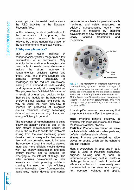
Fig. 1 >Fig. 1 >Fig. 1 >Fig. 1 > The hierarchy of emerging network of
communicating systems consists of a layer of
various sensors monitoring environment, health,
safety etc. connected to mobile phones, tablets
and other mobile applications and to the cloud.
All the layers benefit from thermal management
leading to low power consumption and from
energy scavenging facilitating the expansion of
the swarm [1]./
In a simplified manner one can say that the phonons can manifest themselves as:
Heat: Phonons behave diffusively in systems with large dimensions and follow the laws of statistical physics. Particles: Phonons are treated as wave packets which collide with other particles, defects, interfaces and surfaces. Waves: Phonons are treated as lattice waves, or sound, which can be coherent and can interfere.
Heat is everywhere, in good and in bad. Heat is used in industrial processes, engines, housing and so forth. In information processing heat is usually a challenge because it leads to reduced efficiency, noise and, consequently sets the lower limit to the power consumption, i.e., operation voltages and speed.

EUPHONON project
7777
Nanophononics investigates the behaviour of heat in bulk systems, confined systems, at interfaces and provides tools to optimise the design of information processing devices and circuits. Heat is also a waste which can be recycled by efficient energy harvesting. The recent improvement of the figure of merit of thermoelectric devices stems much from the understanding of heat propagation, the role of different phonon wavelengths and the effects of reduced dimensions.
Ultrafast acoustic scattering uses the particle nature to probe thermal properties of materials and is the basis for development of new imaging methods for medicine, metrology, and structural inspection. Targeted thermally activated treatments may become a new method to cure, e.g., malignant tumours.
Fig. 2 >Fig. 2 >Fig. 2 >Fig. 2 > Manifestation of phonons and some
examples of fields of research and applications
founded on and benefitting from nanophononics./
Typical examples of exploiting acoustic waves are surface and bulk acoustic wave filters which are used in mobile devices. Sound amplification by stimulated emission to create coherent phonons will be the next generation equivalent to optical lasers, enabling realisation of phonon manipulation circuitry in which coherent phonons represent new state variables. The first demonstrations have
required ultra-low temperatures but room temperature operation can be expected in near future in small phononic structures.
The word nanophononics may generate an impression of something marginal, but as shown above and in the following Sections, this field of research has a profound meaning and vast impact in everyday life and very much in the future, particularly in the context of ICT.
3. Challenges and market area
There are several things in everyday life on which nanophononics has a strong impact and can be used to optimise and boost, for example, the energy efficiency, the speed of information processing and the development of new tools for medicine and safety. The main emphasis today can be seen to be on energy issues and ICT but new ideas and applications based purely on phononics are steadily emerging. In the following the role and potential of nanophononics are briefly illustrated.
Fig. 3 >Fig. 3 >Fig. 3 >Fig. 3 > Society is facing several challenges
ranging from energy and environment to
communication, from ageing to well-being and
to security and safety. Nanophononics represents
a new field of research, capable in many cases to
facilitate and accelerate finding solutions by
shedding light on problems related to thermal
issues and generating new approaches to data
communication and ubiquituous technologies./
3.1. Energy and environment
While the exploitation of thermal energy and its conversion into mechanical

8888
EUPHONON project energy with the invention of the steam
engine represented the dawn of the technological era for mankind, heat is nowadays a form of energy, of which we have relatively poor control, both at the macroscopic and the microscopic scale. Phonons are the main heat carriers in semiconductors, insulators, and polymers. Therefore a better understanding of phononic transport over a broad range of size scales and in diverse materials is essential to tackle the challenges related to thermal management and energy scavenging.
With the downsizing of microelectronics systems to below ten nanometre, handling heat dissipation from the hotspots at the nanoscale has turned to be crucial to guarantee the stability of devices and to prevent performance degradation. Similarly, overheating also affects the performances and the reliability of batteries and memories, and, furthermore, cooling is a major issue in photovoltaics. Passive heat dissipation is a viable route to tackle the challenge of thermal management, and can be achieved by employing high thermal conductivity materials. Carbon-based nanostructures, such as graphene and carbon nanotubes, feature the highest phononic thermal conductivity among non-metallic materials, and represent the most suitable candidates for thermal management at the nanoscale [2]. While it is unlikely that the thermal conductivity of these materials can be much improved, it was observed that interactions with substrates may degrade the conductivity substantially [3]. In addition, the heat dissipating modules need to be interfaced well to the active devices by thermal interface materials (TIM) to achieve maximum dissipation efficiency. In this respect the main challenges lie in understanding the transport of thermal phonons at interfaces and eventually in designing
better coupling schemes between the device that needs to be cooled and the dissipating modules and the surroundings. Similar issues apply to the active cooling devices, based on solid state Peltier modules [4]. Here the challenges lie also in the optimization of thermoelectric (TE) materials, promoting TE performances at around and above room temperature, and possibly replacing toxic and/or expensive elements (e.g. Pb or Te) with Earth abundant and environmentally friendly ones.
One of the fastest growing areas requiring thermal management is LED lighting in housing and in cars [5]. The efficiency varies typically between 15 and 30 %, which is at least 75 % higher than the efficiency of incandescent lamps, and is strongly dependent on the operation temperature, as is the lifetime of the LEDs. Only in the United States the expected saving of energy in 2027 arising from widespread use of LED for lighting is 348 TWh, i.e., equivalent to 44 GW power plants [6]. The proper design and control of the heat in the lighting modules will be of crucial importance to achieve the targeted savings in energy.
Fig. Fig. Fig. Fig. 4444 >>>> Use of LEDs in lighting is increasing very
rapidly. To maintain the efficiency and the long
lifetime of the LEDs, thermal management of
the packages is becoming crucial./
In engines and power plants a significant amount of energy is lost as waste heat. It was estimated that more than 60% of the energy produced by fossil fuels goes into waste heat. Similarly, heat dissipation

EUPHONON project
9999
represents a major cost for households. Thermoelectric devices that convert heat to electric power, even though at fairly low levels of efficiency, typically below 10%, may turn into a valuable resource to harvest waste heat. So far, the use of TE modules has been limited to niche applications by the intrinsic limits of materials performances, which is usually express as the figure of merit ZT. ZT is given by the ratio between the electronic power factor and thermal conductivity, mostly dominated by phonons. The main issue is that crystalline materials with high TE power factor also have a relatively high thermal conductivity, which limits the ZT. The paradigm would be to design materials that behave as electron crystals and phonon glasses [7]. This can be achieved by nanostructuring [8]. The idea is to introduce phonon scatterers at length scales that would block the propagation of heat but would not perturb significantly the electronic transport. This approach has produced encouraging results for traditional TE materials, e.g., bismuth telluride, as well as for silicon [9]. More recently hierarchical nanostructuring from the atomic to the mesoscopic scale yielded exceptionally high TE figure of merit [10]. In spite of these success stories, materials design still relies on simplistic models [11] that have been challenged by recent experimental "spectroscopic" measurements of phonon mean free paths [12]. Much deeper understanding of the effects of nanostructuring and dimensionality reduction on phonon transport is needed to design ultimate TE materials and TE generators, tuned to targeted applications, with good control on the temperature and power ranges. This is a multidisciplinary task that will greatly benefit from collaboration of statistical physicists, molecular modellers, experimental physicists, engineers, and materials chemists.
Temperature control is an important factor in photovoltaics. In silicon photovoltaics cells the efficiency drops on average -0.45%/ºC, calling for passive or active cooling to keep the cell temperature in the range of 20-60 ºC and maintain the power production [13]. The temperature control can again be achieved by proper design of the heat flow in the PV cell casing and to the surroundings. This will be an important market when the energy production is shifting from the fossils to solar energy.
Key findings and outcome from the EUPHONON workshops
Topic Details and relevance
Heat Manipulate the spectrum of heat.
Thermal management
Manipulate heat exploiting rectification and nanostructures.
Energy harvesting
Decouple electrons and phonons using nanostructuring.
3.2. Information processing
It is well known that phonons are the main cause for carrier scattering in transistors at around room temperature, limiting the mobility. Electron-phonon scattering represents a rather fundamental phenomenon and is more or less unavoidable. It has been shown that driving the devices in volume inversion mode the phonon scattering can be reduced due to reduced number of available states in the k-space [14]. The size of today’s transistors is smaller than the mean free path of phonons, leading to a situation that the energy dissipation is not anymore concentrated in the hot spot at the drain side of the channel but the dissipation can take place anywhere in the volume with size of the phonon mean free path. This is very challenging to the thermal management of the devices and circuits. The temperature defines the distribution of the carriers and, consequently, sets the lower limit to the operation voltage and the power

10101010
EUPHONON project consumption, and the speed.
Nanophononics provides tools to understand the propagation and scattering of phonons in these small volumes with a large number of different materials and interfaces, and helps to build a picture of the flow of energy and accumulation of heat, facilitating the optimisation of the operation of transistors and circuits.
The heat dissipation in ICs is a cumulating effect that materialises in the operation of data centres in which more than half of the power is nowadays consumed in cooling the computers and data banks. The power consumption of data centres only in the US was 91 billion kWh in 2013 [15]. Here the problem is not restricted only to the thermal budget arising from the operation of billions of transistors. The packaging, including thermal interfacing, constitutes the main problem and even a small improvement in the thermal management would produce huge savings in energy and, consequently, reduce the environmental load.
Fig. 5 >Fig. 5 >Fig. 5 >Fig. 5 > Typical distribution of the energy consumption
in a data centre [16]./
Surface and bulk acoustic wave devices (SAW, BAW) represent a good example of the utilization of “sound” in microelectronics. The devices transform electric signals to acoustic field, or standing waves in an acoustic cavity, for filtering and back to electric signal again, being the corner stones of current mobile applications. The operating frequencies at the moment are below 10 GHz, but can be brought higher with proper design.
The modulation of electrical current at high speed, or electron pumping, can be realized with coherent phonons. The carriers are usually photoexcited and locally trapped by the strain field of the SAW which propagates in a controlled direction. By playing with different surface acoustic waves, multiplexing the electronic signal on chip becomes possible [17-18]. There are current limitations for the optimization of such functionality like the efficiency of optical pumping, to create high enough strain to have high enough potential energy variation to trap the spin polarized carriers. Phonon-induced fast strain fields can also be used to manipulate barrier heights in junctions and the effect has been demonstrated in Schottky junctions [19].
The emerging field of spintronics intends to develop information devices based on spin current and spin waves or magnons, having the advantage of preventing the joule heating which is one of the main problems in charge current based devices. Spin valve devices based on giant magnetoresistance, i.e., hard disks have been around already for long times. The spintronics community works in a different direction and intend to employ coherent acoustic phonons to manipulate the spins, either to launch spin waves [20,21], or to modulate the magnetization [22-24]. These phenomena arise from the magneto-elastic coupling but the current understanding of generation of spin waves by strain as well as the fast manipulation of spins with strain are both in their infancy. The spins can also be manipulated by surface acoustic waves by transporting spin-polarised electrons by the strain field induced troughs and crests in the energy topology of the band gap. This has been demonstrated in GaAs [25]. The limitation is the low spin current level.
Cavity optomechanics explores the parametric coupling of an electromagnetic cavity field with a mechanical degree of

EUPHONON project
11111111
freedom [26]. The photons are circulating in an optical cavity and interact with a micro-or nanomechanical resonator. Similarly, on-chip coupling between a microwave cavity and a mechanical mode is employed. Optomechanics is a fast growing field which consisted of 3 or 4 research groups a decade ago and now active with more than 60 groups. Phonons serve two purposes: First, they are employed to describe the discrete mechanical mode, e.g., a flexural mode of a micro- or nanostructured device or a localized acoustical mode in a phononic crystal cavity. Secondly, phonons play an important role in the decoherence of optomechanical devices in which energy radiation into the clamping supports is typically one of the dominating dissipation mechanisms.
Controlling the interaction between light and phonons allows taking advantage of the best of both worlds. Furthermore, miniaturization enables devices such as on-chip whispering gallery devices or optomechanical crystals, which are highly integrable into arrays or metamaterials, or with semiconductor components such as waveguides or lasers. They show a real promise for integrated technologies taking advantage of the maturity of Si microelectronics and GaAs or InP optoelectronics technologies.
At the same time, optomechanics can be envisioned to act as building blocks for information storage and processing devices, both in the classical and quantum regime. In theoretical proposals, optomechanical concepts are discussed for photon routing, controlled photon-photon interaction, information storage and retrieval, both classically and quantum. The optomechanical interaction can induce optical non-linearities such as an effective Kerr interaction that can be engineered via the phononic degree of freedom. Like in non-linear optics, this enables photon processing (logic gates,
multiplexing, amplification). More generally, in these emerging concepts, long-lived vibrational modes will be employed for information storage or transduction between optical photons used in communication and microwave photons easily compatible with chip-based data processing.
Another very active area of research is the field of nanomechanics. Nanoelectromechanical systems (NEMS) are scaled-down versions of the well-known MEMS. The technology of NEMS has vast potential for sensing applications, not only for their ultra-high sensitivity enabling these devices to resolve a single electron spin [27] or very few nuclear spins [28], forces down to the zeptonewton regime [29] or masses of only a few yoctograms [30], but also for mass-market applications [31] such as gyroscopes or other types of accelerometers [32]. Furthermore, NEMS can be engineered to be CMOS compatible such that full integration of sensors [33], switches [34] or narrow-band filters into CMOS architectures can be envisioned. Another area of interest is bioNEMS, with a vast potential in biosensing applications [35]. As for optomechanical systems, a clear connection between NEMS and phononics is apparent: The mechanical eigenmodes of the system, e.g., the flexural modes of a string resonator or a membrane, represent discrete acoustic phonons. Secondly phonons importantly contribute to the decoherence and dissipation of nanomechanical devices, which is frequently dominated by energy radiation into the clamping supports.
For information technologies based on photonics, the modulation of light and the acoustic surface resonators are key issues in the data processing and filtering. Light modulation takes place through different mechanisms like the electro-optic process, wavelength-division multiplexing and acousto-optic interaction with bulk

12121212
EUPHONON project and surface acoustic waves. The acousto-
optic modulation is based on the interaction of light with acoustic phonons, is a well-established technique that works well in the MHz regime. These devices are usually based on biased-piezoelectric materials (ZnO, LiNbO3, PbZrTiO3) and are frequency is typically limited to a few GHz due to the electronics. Going higher in frequency range, from a few tens of GHz to THz, and towards integrated elasto-optic modulators as well as surface acoustic waves devices have great potential in the next generation ICT devices [36-38]. To achieve this, efficient and miniaturized sources of coherent acoustic phonons. Only the ultrafast laser-induced processes can produce such high frequency and confined acoustic phonons are needed. The limitation at the moment is the small phonon strains (10-4) obtained by optical excitation by lasers [39-40]. Increasing the efficiency of the light energy conversion into mechanical energy is very challenging and new physical processes of light-matter interaction with high frequencies at GHz to THz and strain of 10-3 is required. The effort made in this direction will also certainly be useful for the community of optomechanics, to go beyond the radiation pressure approaches mainly used at the moment in the MHz-GHz optomechanics devices [41].
By means of light-induced back-action the mechanical mode under consideration can be cooled into the quantum regime. In recent years, major breakthroughs have been achieved with optomechanical crystal (phoXonic) structures (X=n,t) [42] as well as with microwave analogies of optomechanical systems, so called cavity electromechanical devices [43]. Reaching a regime where quantum behavior emerges both for light and for phonons enables not only boosting the performance of some target applications, e.g., information treatment, quantum states transfer between RF and optical
fields, but also holds promise for a new type of "quantum technology". Exploration of non-classical phenomena allows targeting unresolved questions in fundamental physics such as the entanglement of macroscopic objects or tests of quantum theories involving gravity. Furthermore, optomechanical systems represent a versatile platform for the development of ultrasensitive, quantum limited sensing elements.
Quantum computing represents a long term paradigm to finally crack some of the hurdles related to information processing. It is capable to solve a few problems much faster than even the conventional supercomputers. Quantum information and quantum computation relies on the concept of entanglement of qubits. In reality the quantum systems are not isolated and will be influenced by surroundings and the interactions lead to decoherence of the entanglement. For solid state qubits, although operating at mK range, it is crucial to minimise or completely eliminate phonons and fluctuations in the vicinity of the qubits [44]. This again calls for proper understanding and design of the qubits and their coupling to the surroundings. Recently an opposite approach was reported. Here travelling phonons are coupled to an artificial atom and represent state variables to perform computing [45].
Key findings and outcome from the EUPHONON workshops
Topic Details and relevance
Optomechanics, plasmonics and spintronics
Photon-phonon, plasmon-phonon and spin-phonon coupling.
3.3. Health and well-being
THz spectroscopy has a great promise in the field of medical imaging [46]. It can reveal skin cancer and other tumours at early stage and give images of structures

EUPHONON project
13131313
which are optically opaque. In addition to imaging, the THz radiation can couple to the vibrational modes of molecules and can provide information of bonds and used for spectroscopy. For example the four nucleobases of DNA have different vibrational spectra and can be differentiated.
Fig. Fig. Fig. Fig. 6666 >>>> Absorption coefficients of the nucleabases
A, C, G and T of DNA measured at 10 K (solid lines)
and at 300 K (dashed lines) [from Ref 46]./
THz technology can also provide tools to localised drug delivery and hyperthermia treatments [47]. Another dimension for well-being is the preventive health monitoring at home. Data can be collected by various autonomous sensors, e.g., blood pressure or glucose level, potentially even continuously, and the information is sent to medical centres and data banks for inspection, see Figure 1. This type of preventive monitoring would rely on internet of things and would need low power devices and, potentially, exploit energy scavenging.
Key findings and outcome from the EUPHONON workshops
Topic Details and relevance
Ultra-fast phenomena
Sensing of mechanical properties for tumoral cell detection.
Hyperthermia Magnetic Nanoparticles based hyperthermia treatments.
3.4. Safety and security
THz technology has also been used as screening technology, for example, at the airports to prevent people entering vehicles with concealed weapons, including non-metal edged weapons. The vibrational frequencies of the chemical bonds allows the recognition of, for example, explosives [48]. The need of security screening and loss-preventing applications for retail logistics has already led to establishing companies producing tools and equipment [49]. THz technology is also providing tools for metrology and standards. Although hampered currently by the lack of stable sources and detectors, the number of companies producing instruments for power measurement and time and frequency domain spectroscopy is steadily increasing [50].
Where the THz spectroscopy is falling short is the spatial resolution. The resolution of THz imaging is in the range of 100’s of µm, the consequence of the electromagnetic wavelength used, while in several applications much higher resolution is needed. Ultra-fast acoustic phonons provide a means to achieve sub-micron resolution [51]. Ultra-fast optical pulses to generate thermoelastic excitation in a thin metal film are used to generate picosecond acoustic phonons which can be used to non-invasive imaging with sub-100 nm resolution. The phonons scatter from inclusions and interfaces in the matrix and enable even 3-dimensional non-destructive imaging of objects. This type nanoscale ultrasonics

14141414
EUPHONON project can be used in inspection of microscale
cracks and inhomogeneous spots in, e.g., vessels used in chemical industry and in nuclear plants. The 3D imaging, however, requires new type of algorithms and heavy computation, making the approach challenging [52].
Key findings and outcome from the EUPHONON workshops
Topic Details and relevance
THz spectroscopoy
Safety and screening.
Fig. Fig. Fig. Fig. 7777 >>>> Interdependencies between different
phonon presentations and key topics./
4. Global position
The global situation is described in more detail in the EUPHONON Position Paper. Briefly, at the moment the global competition mainly involves the US and China which have recently invested heavily in the nanophononics research. The USA National Science Foundation and the Chinese Academy of Science have already established ties for collaboration in the form of bilateral workshop and a school for post graduates.
In China Prof. Baowen Li has established the “Center for Phononics and Thermal Energy Science” [53] in Shanghai, recruiting 20 professors and organizing biannual international schools and conferences. The funding is several tens of millions $. In the US the Department of
Energy (DoE) is funding of Centers of Excellence in Basic and Applied Energy Research running into several 10’s of millions of dollars. For example, MIT received 15M$ over 5 years for one of its Arpa-e Center [54] and this sort of funding has been regular for 20 years. In Europe several teams have the position as international leaders and have pioneered several phononics related activities but the field has been rather fragmented and only recently a more integrated community has started to develop. The fragmentation has reflected also in the relatively limited resources available for research. One of the key targets of the EUPHONON coordination actions has been to strengthen the integration and provide ideas how to further enhance the nanophononics activities in Europe.
5. European ecosystem
The ecosystem of nanophononics in Europe is composed of groups in academia, research institutes, large companies and SMEs and start-ups. This is reflected in the list of members in the EUPHONON community, with the number of members currently exceeding 50 from 15 different countries [55]. The academic groups and research institutes cover a broad range of activities from very basic physics to experimental work and applied science. Included are solid state physics, statistical physics and thermodynamics, material sciences and biosciences as well as engineering.
The interests of industry include various aspects of thermal management related to packaging, temperature control and energy harvesting. Thermal interface materials play a big role in the electronics and in increasing amount in the lighting industry with several companies producing packages, the TIMs and their testing tools. The IC, memory and MEMS chip producers have to more and more
EUPHONON project
15151515
take into account the thermal aspects in the circuit design, leading to the uptake of nanophononics in the mainstream industries.
There are also start-up companies emerging from academia and research institutes which produce new types of equipment for example for characterisation of ultra-fast phenomena and THz imaging [56].
The European Commission has supported the field by funding several research projects related to thermal management, energy harvesting, and projects focusing on nanophononics and optomechanics. These include projects such as NANOTEG, NANOPACK, NANOTHERM, ZEROPOWER, MERGING, TAILPHOX, NANOPOWER, UPTEG, MINOS, QNEMS, cQOM, iQOEMS and QUANTIHEAT [57]. The list is not exhaustive but gives an idea of the increasing activity and importance of the field. National funding agencies have also started to invest in phononics and related topics.
6. Conclusions
The importance and impact of nanophononics are increasing in thermal management to enhance the operation and speed of ICT devices and to reduce their power consumption. In controlling the heat it is crucial to understand the propagation of phonons in different media and across interfaces. This reflects directly, for example, to the efficiency of data processing and lighting. The emerging fields include health and medicine and security for which phonons provide new approaches and applications for imaging and spectroscopy. Nanophononics tackles also the very fundamental issues in physics and forms an interesting and broad topic for education.
It is essential to create a research agenda for nanophononics in Europe and establish a dedicated work program to
support this research field to avoid lagging too much behind the US and Asia, especially China.
Acknowledgements
The editors acknowledge the support of the EC FET ICT project EUPHONON grant agreement 612086. They were assisted by Drs Jose Ordonez, Martin Schubert and Francesc Alzina. They are grateful to several colleagues who helped with the organisation of the events upon which this document was built, especially Prof. Bahram Djafari-Rouhani and Dr. Erwan Guillotel.
References
[1] Jan M. Rabaey , 2011 Symposium on VLSI Circuits Digest of Technical Papers
[2] Balandin, A. A. Thermal properties of graphene and nanostructured carbon materials. Nat Mater 10, 569–581 (2011). ; Xu, X., et al., Length-dependent thermal conductivity in suspended single-layer graphene, Nature Communications (2014).; Yan et al. Nature Communications 3, 827 (2012)
[3] Seol, J. H. et al. Two-Dimensional Phonon Transport in Supported Graphene, Science 328, 213–216 (2010)
[4] Majumdar, A. Thermoelectric devices: helping chips to keep their cool, Nature Nanotechnology 4, 214–215 (2009)
[5] Lasance, C. J. M., and Poppe, A. 2014. Thermal Management for LED Applications, Springer Science+Business Media, New York
[6] http://energy.gov/energysaver/articles/led-lighting
[7] Snyder, G. J. & Toberer, E. S. Complex thermoelectric materials, Nat Mater 7, 105–114 (2008)
[8] Majumdar, A., Enhanced Thermoelectricity in Semiconductor

16161616
EUPHONON project Nanostructures, Science 303, 777–
778 (2004) [9] Poudel, B. et al. High-thermoelectric
performance of nanostructured bismuth antimony telluride bulk alloys, Science 320, 634–638 (2008). ; Yu, J.-K., Mitrovic, S., Tham, D., Varghese, J. and Heath, J. R. Reduction of thermal conductivity in phononic nanomesh structures, Nature Nanotechnology 5, 718–721 (2010)
[10] Biswas, K. et al. High-performance bulk thermoelectrics with all-scale hierarchical architectures, Nature 489, 414–418 (2012)
[11] Callaway, J. Model for lattice thermal conductivity at low temperatures, Phys Rev 113, 1046 (1959)
[12] Minnich, A. J. et al. Thermal Conductivity Spectroscopy Technique to Measure Phonon Mean Free Paths, Phys. Rev. Lett. 107, 095901 (2011)
[13] Dengfeng Du, Jo Darkwa, Georgios Kokogiannakis, Thermal management systems for Photovoltaics (PV) installations: A critical review, Solar Energy 97, 238–254 (2013)
[14] F. Gamiz, J. B. Roldan, A. Godoy, P. Cartujo-Cassinello, and J. E. Carceller, J. Appl. Phys. 94, 5732 (2003)
[15] http://www.nrdc.org/energy/data-center-efficiency-assessment.asp
[16] http://blog.infotech.com/tag/data-center/page/4/
[17] S. Hermelin, S. Takada, M. Yamamoto, S. Tarucha, A. D. Wieck, L. Saminadayar, C. Bäuerle, T. Meunier, Electrons surfing on a sound wave as a platform for quantum optics with flying electrons, Nature 477, 435–438 (2011)
[18] S. Buyukkose , A. Hernández-Mínguez, B. Vratzov , C. Somaschini , L. Geelhaar , H. Riechert , W. G. van der Wiel , P. V. Santos, High-frequency acoustic charge transport in GaAs nanowires, Nanotechnol. 25 , 135204 (2014)
[19] D.M. Moss, A.V. Akimov, B.A. Glavin, M. Henini and A.J. Kent, Ultrafast strain-induced current in a GaAs
Schottky diode, Phys. Rev. Lett. 106, 066602 (2011)
[20] M. Bombeck, A. S. Salasyuk, B. A. Glavin, A. V. Scherbakov, C. Brüggemann, D. R. Yakovlev, V. F. Sapega, X. Liu, J. K. Furdyna, A. V. Akimov, and M. Bayer, Excitation of spin waves in ferromagnetic (Ga,Mn)As layers by picosecond strain pulses, Phys. Rev. B 85, 195324 (2012)
[21] K. I. Doig, F. Aguesse, A. K. Axelsson, N. M. Alford, S. Nawaz, V. R. Palkar, S. P. P. Jones, R. D. Johnson, R. A. Synowicki, J. Lloyd-Hughes, Coherent magnon and acoustic phonon dynamics in tetragonal and rare-earth-doped BiFeO3 multiferroic thin films, Phys. Rev. B, 88, 094425 (2013)
[22] Kim, J.-W., Vomir, M. and Bigot, J.-Y., Ultrafast magnetoacoustics in nickel films, Phys. Rev. Lett. 109, 166601 (2012)
[23] M Krawczyk and D Grundler, Review and prospects of magnonic crystals and devices with reprogrammable band structure, J. Phys.: Condens. Matter 26 123202 (2014)
[24] Oleksandr Kovalenko, Thomas Pezeril, and Vasily V. Temnov, New Concept for Magnetization Switching by Ultrafast Acoustic Pulses, Phys. Rev. Lett. 110, 266602 (2013)
[25] A. Hernández-Mínguez , K. Biermann , R. Hey , P. V. Santos, Spin transport and spin manipulation in GaAs (110) and (111) quantum wells, Phys. Status Solidi B 251 , 1736 (2014)
[26] Aspelmeyer, Kippenberg and Marquardt, arXiv:1303.0733v1; Cavity Optomechanics: Nano- and Micromechanical Resonators Interacting with Light, Eds: Aspelmeyer, Kippenberg & Marquardt, Springer, Berlin (2014)
[27] Rugar et al., Single spin detection by magnetic resonance force microscopy, Nature 430, 329 (2004)
[28] Degen et al., Nanoscale magnetic resonance imaging, PNAS 106, 1313 (2009)
EUPHONON project
17171717
[29] Moser et al., Ultrasensitive force detection with a nanotube mechanical resonator, Nature Nano 8, 493 (2013)
[30] Chaste et al., A nanomechanical mass sensor with yoctogram resolutio, Nature Nano 7, 301 (2012)
[31] see e.g. https://technology.ihs.com/389490/booming-iphone-and-ipad-sales-make-gyroscopes-the-top-consumer-and-mobile-mems-device-in-2011
[32] Chen et al., Sensors 9, 1330 (2009), Krause et al., Nature Photonics 6, 768 (2012)
[33] Bargatin et al., Large-Scale Integration of Nanoelectromechanical Systems for Gas Sensing Applications, Nano Lett. 12, 1269 (2012)
[34] Ng et al., High density vertical silicon NEM switches with CMOS-compatible fabrication, Electronics Lett. 47, 759 (2011)
[35] Arlett et al., Comparative advantages of mechanical biosensors, Nature Nano 6, 203 (2011)
[36] D. Shin, Y. Urzhumov, D. Lim, K. Kim, D. R. Smith, A versatile smart transformation optics device with auxetic elasto-electromagnetic metamaterials, Sci. Report 4, 4084 (2014)
[37] M. Schubert, M. Grossman, O. Ristow, M. Hettich, A. Bruchhausen, E. C. S. Barretto, E. Scheer, V. Gusev, T. Dekorsy, Spatial-temporally resolved high-frequency surface acoustic waves on silicon investigated by femtosecond spectroscopy, Appl. Phys. Lett. 101, 013108 (2012)
[38] A. Crespo-Poveda , R. Hey , K. Biermann , A. Tahraoui , P. V. Santos , B. Gargallo , P. Muñoz , A. Cantarero , M. M. de Lima, Synchronized photonic modulators driven by surface acoustic waves, Jr. Opt. Express 21, 21669 (2013)
[39] C. Thomsen, H.T. Grahn, H.J. Maris, J. Tauc, Surface generation and detection of phonons by picosecond light pulses, Phys. Rev. B 34 (1986) 4129
[40] P Ruello, VE Gusev, Physical mechanisms of coherent acoustic phonons generation by ultrafast laser action, Ultrasonics, (2014)
[41] I. Favero, The stress of light cools vibration, Nature. Phys. 8, 180–181 (2012)
[42] See e.g. Eichenfield, Nature 462, 78 (2009), Safavi-Naeini, PRL 108, 033602 (2012), Safavi-Naeini, PRL 112, 153603 (2014)
[43] See e.g. Teufel, Nature 475, 359 (2011), Palomaki, Science 342, 710 (2013)
[44] V. N. Golovach et al., Phys. Rev. Lett. (2004) 016601
[45] M. V. Gustafsson et al., Science 346 (2014) 207-211
[46] E. Pickwell-MacPherson and V. P. Wallace, Terahertz pulsed imaging - A potential medical imaging modality? Photodiagnosis and Photodynamic Therapy 6 (2009) 128-134
[47] H.-K. Son, Nanotechnology Topical Review 24 (2013) 214001
[48] X.-C. Zhang, Phys. Med. Biol. 47 (2002) 3667-3677
[49] See, for example http://asqella.com/. [50] Z. Popovic and E. N. Grossman, IEEE
Trans. Terahertz Sci. Technol. 1 (2011) 133-144
[51] B. C. Daly et al., Appl. Phys. Lett. (2004) 5180-5182
[52] R. Li Voti et al., Intl. J. Thermophysics 26 (2005) 1833-1848
[53] http://phononics.tongji.edu.cn/ehome.shtml
[54] http://s3tec.mit.edu/ [55] www.euphonon.eu/EPH/index.php [56] http://www.menlosystems.com/en/prod
ucts/synchronization-stabilization-and-asops-systems/asops/, https://www.thorlabs.us/newgrouppage9.cfm?objectgroup_id=4711, http://asqella.com/ , Z. Popovic and E. N. Grossman, IEEE Trans. Terahertz Sci. Technol. 1 (2011) 133-144
[57] http://www.project-nanoteg.com/, http://project-nanotherm.com/

nanojobs
18181818
• Postdoc position: "Development of polymeric linkers and graphene based matrixes for the embedment of Si nanoparticules in electrochemical energy storage electrode materials" Contact: [email protected] (CEA, France) • PhD position: "Inelastic Neutron Scattering study of
zeolite acidity"
Contact: [email protected] (UPV-CSIC, Spain) • Postdoc position: "Coupling of proteins and/or antibodies to carbon nanotube tags" Contact: [email protected] (Université de Montréal, Canada) • Job position: "PhD/Experienced Technologist" Contact: [email protected] (AIN, Spain) • Postdoc position: "Micro and Nanoscale Heat Transfer" Contact: [email protected] (Université de Reims Champagne-Ardenne, France) • PhD position: "Thermal Nano-contact and influencing parameters in Scanning Thermal Microscopy" Contact: [email protected] (CNRS-CETHIL, France)
• Postdoc position: "Modelling for Near-field Scanning Probe Microscopy" Contacts: [email protected] (CNRS-CETHIL, France)
• Tenure-Track position: "Tenure-Track position in Catalysis by Nano-Engineered Materials and Devices" Contact: [email protected] (University of Twente, Netherlands)
• PhD position: "Modelling of functionalized gold nanoparticles for antibiotic therapy: morphology – stability relationships" Contact: [email protected] (CEMES-CNRS, France) • PhD position: "Molecular Engineering for Targeted Cancer Therapy" Contact: [email protected] [email protected] (Institut Curie, France)
• PhD position: "Toward coherent ultrafast transmission electron microscopy" Contact: [email protected] [email protected] (CEMES-CNRS, France)
• PhD position: "PhD Student Position in the field of Novel Piezoelectric Materials" Contact: [email protected] (Fraunhofer IAF, Germany)
More info about these jobs available at www.phantomsnet.net/jobs/

Visualizing superconductive
coupling over atomic steps
nanoresearch Highlights
19191919
International Center for Materials Nanoarchitectonics (WPI-MANA) National Institute for Materials Science 1-1 Namiki, Tsukuba, Ibaraki, 305-0044 Japan www.nims.go.jp/mana/research/highlights
Scanning tunnelling microscopy imaging under differing magnetic fields gives fundamental insights into the behavior of supercurrents and vortices on the surface of indium-doped silicon films.
Superconductors have effectively zero resistance and act as perpetual carriers of electric current with no need for a connected power source. As such they have many applications in electronics. One of the thinnest two-dimensional materials ever created, called Si(111)-(√7 x √3)-In –individual indium metal atoms added to a silicon surface - recently surprised scientists with its superconducting abilities. The race is now on to find out how and why this silicon surface is capable of superconductivity, as well as what uses it may have.
Takashi Uchihashi and co-workers at the International Center for Materials Nanoarchitectonics, Tsukuba, together with scientists across Japan, have now uncovered the underlying structures and the behavior of currents on the surface of Si(111)-(√7 x √3)-In which provide clues to its superconductivity.
The silicon surface comprises individual terraces separated by steps measuring the height of a single atom (‘atomic steps’). These steps could potentially interrupt, or decouple, neighboring terraces and break the current flowing over large surfaces. Uchihashi and his team used a scanning tunnelling microscope in order to verify how superconductivity occurs in the presence of atomic steps and terraces. The team applied different magnetic fields, which influenced the strength of the current and the presence of associated vortices.
By taking a series of images of the silicon, the team uncovered a pattern of supercurrent vortices present on the silicon surface. Two vortex types were present. Pearl vortices were present on the terrace surfaces, and appeared as bright round features in the images. However, at the atomic steps the vortices appeared to become trapped and altered in character. These elongated ‘Josephson vortices’ give evidence that the atomic steps work as so-called Josephson junctions, allowing coupling to occur across stepped terraces and enabling supercurrents to flow. The idea was firmly established with the help of microscopic theoretical calculations.
Fig.Fig.Fig.Fig. 1 >1 >1 >1 > Scientists at the International Center for
Materials Nanoarchitectonics have uncovered
how supercurrents flow over atomic steps and
terraces on indium-covered silicon surface.
Vortices trapped at the atomic steps change
their characters from Pearl to Josephson
vortices (from A to C). These reflect change in
strength of Josephson coupling between the
neighboring terraces.
Reference
“Imaging Josephson vortices on the surface superconductor using a scanning tunnelling microscope”, Shunsuke Yoshizawa, Howon Kim, Takuto Kawakami, Yuki Nagai, Tomonobu Nakayama, Xiao Hu, Yukio Hasegawa, Takashi Uchihashi, Physical Review Letters, (2014) (highlighted as an Editors' Suggestion) Doi: 10.1103/PhysRevLett.113.247004

Hydrocarbon photocatalysts get in
shape and go for gold
20202020
WPI/MANA
International Center for Materials Nanoarchitectonics (WPI-MANA) National Institute for Materials Science 1-1 Namiki, Tsukuba, Ibaraki, 305-0044 Japan www.nims.go.jp/mana/research/highlights
A combination of semiconductor catalysts, optimum catalyst shape, gold-copper co-catalyst alloy nanoparticles and hydrous hydrazine reducing agent enables an increase of hydrocarbon generation from CO2 by a factor of ten.
“Solar-energy-driven conversion of CO2 into hydrocarbon fuels can simultaneously generate chemical fuels to meet energy demand and mitigate rising CO2 levels,” explain Jinhua Ye and her colleagues at the International Center for Materials Nanoarchitectonics in their latest report. Now the research team have identified the conditions and catalysts that will maximise the yield of hydrocarbons from CO2, generating ten times previously reported production rates.
Carbon dioxide can be converted into a hydrocarbon by means of ‘reduction reactions’ - a type of reaction that involves reducing the oxygen content of a molecule, increasing the hydrogen content or increasing the electrons. In photocatalytic reduction of CO2 light activates the catalyst for the reaction.
Ye and her team introduced four approaches that each contributed to an increased reaction rate. First, they combined two known semiconductor photocatalysts strontium titanate (STO) and titania (TiO2) – which led to the separation of the charges generated by light and hence a more effective photocatalyst. Second, the high surface area of the nanotubes was made greater by holes in the tube surfaces, which
enhances catalysis by increasing the contact between the gases and catalysts. Third, the tubes were decorated with gold-copper (Au3Cu) nanoparticle co-catalysts to further enhance the catalysis, and fourth, they used hydrous hydrazine (N2H4•H2O) as the source of hydrogen.
Although the high hydrogen content of hydrous hydrazine is widely recognised in the context of hydrogen storage there are no previous reports of its use for reduction reactions. The researchers demonstrated that the reducing properties of hydrous hydrazine were so great that oxidation of the co-catalytic nanoparticles – a problem when water or hydrogen are used – was avoided.
The researchers conclude their report, “This opens a feasible route to enhance the photocatalytic efficiency, which also aids the development of photocatalysts and co-catalysts”.
Reference
“Photocatalytic reduction of carbon dioxide by hydrous hydrazine over Au–Cu alloy nanoparticles supported on SrTiO3/TiO2 coaxial nanotube arrays”, Qing Kang, Tao Wang, Peng Li, Lequan Liu, Kun Chang, Mu Li, Jinhua Ye, Angewandte Chemie International Edition, (2015), 54, 841 –845. DOI: 10.1002/anie.201409183

21212121
WPI/MANA
Fig. 1 >Fig. 1 >Fig. 1 >Fig. 1 > A combination approach
increases the generation of
hyrdrocarbons from CO2 by a
factor of ten. A) Scanning electron
microscope image, the white
arrows indicate the holes in the
tubewall; B) Xray diffraction pattern
of strontium titanate (STO)-titania
(TiO2) coaxial nanotube arrays; C)
transmission electron microscope
image of Au3Cu@STO/TiO2
nanotube arrays; D) High-
resolution transmission electron
microscope image and fast Fourier
transform pattern of Au3Cu
nanoparticles./
Supercomputing in materials science:
First-principles simulations of large molecules
International Center for Materials Nanoarchitectonics (WPI-MANA) National Institute for Materials Science 1-1 Namiki, Tsukuba, Ibaraki, 305-0044 Japan www.nims.go.jp/mana/research/highlights
Large-scale calculation capable of handling material systems containing 100 to 1,000 times more atoms than conventional methods
Matter is composed of atoms, and its physical properties are determined by the complex interactions between atoms and electrons. Theoreticians use quantum mechanics to calculate the forces between atoms, and the behaviour of electrons in materials. Specifically, first-principles simulations are based on quantum mechanics, and are a powerful technique widely used to elucidate diverse properties of matter and materials at the atomic scale.
However, the size of the systems modelled with conventional first-principles methods
is limited to only a few hundred atoms (in most cases) because the complexity and time required for simulations increases as the cube of the number of atoms being modelled.
Now, a research team led by David Bowler, NIMS MANA and UCL London Centre for Nanotechnology, and Tsuyoshi Miyazaki at NIMS, has successfully developed a highly efficient, large-scale first-principles simulation method for simulating the dynamics of very large systems, containing 100-1,000 times more atoms than conventional methods (up to millions of atoms).
This method provides the means of performing atomic and electronic structure simulations of biological molecules and complex matter, including nanostructured materials, for which conventional methods cannot be used.
The research team has been pursuing the development of a calculation method

22222222
WPI/MANA capable of performing highly efficient large-
scale simulations of dynamics. Here, by introducing a new technique where the time required increases linearly with the number of atoms and utilizing supercomputers, namely the “K computer” and FX10 installed at RIKEN and the University of Tokyo, respectively, the team successfully performed first-principles dynamical simulations of systems comprising more than 30,000 atoms, which is 100 times larger than is usual with
conventional methods. Their success will pave the way for simulation of very large systems including up to millions of atoms.
Reference
"Stable and Efficient Linear Scaling First-Principles Molecular Dynamics for 10,000+ atoms", M. Arita, D. R. Bowler, T. Miyazaki, Journal of Chemical Theory and Computation, 10, 5419 (2014). DOI: 10.1021/ct500847y
Calculation time by ”K computer”
Elapsed time (sec/step)
Number of atoms
16 atoms/core
8 atoms/core
4 atoms/core
Million atoms
Fig. 1 >Fig. 1 >Fig. 1 >Fig. 1 > Calculation time of O(N) first-principles calculation program run by the ”K computer”
(1CPU = 8 cores). The calculations were performed on silicon systems. The horizontal axis shows
the number of atoms, indicating that first-principles calculation of million atom systems is possible.
The O(N) method combined with ideal parallel performance of the program (twice the number of
CPUs achieving twice the amount of calculation) can calculate systems containing twice the number
of atoms in the same time by doubling the number of CPUs./
Fig. Fig. Fig. Fig. 2222 >>>> Snapshot structure from first-principles
simulation of DNA in water medium using the
calculation method developed by the research. The
forces between atoms are calculated by first-
principles calculation (joint research with RIKEN)./

23232323
WPI/MANA
International Center for Materials Nanoarchitectonics (WPI-MANA) National Institute for Materials Science 1-1 Namiki, Tsukuba, Ibaraki, 305-0044 Japan www.nims.go.jp/mana/research/highlights
Electrochemical techniques produce tuneable porous gold films, where the empty spaces enhance light scattering and sensing signals.
Non-metallic mesoporous structures have already demonstrated potential for applications in gas storage, separation, catalysis, ion-exchange, sensing, polymerization and drug delivery. Metal mesoporous films could have fascinating and useful optical properties as they are effectively the inverse of nanoparticle arrays. Now for the first time a collaboration of researchers in Japan, Turkey, Korea and Sweden demonstrate a simple approach for producing metal films with regular tuneable mesopores, and show their potential for high-sensitivity optical detection.
When light is incident on nanostructures of noble metals such as gold, the electrons oscillate collectively – a so-called plasmon – and this greatly enhances the electromagnetic field close by. According to Babinet’s principle in optics, the inverse structure – a mesoporous film – should lead to similar local electromagnetic field enhancements, but as Yamauchi and his colleagues point out in their report, controlling gold crystal growth well enough to produce mesoporous films has so far been difficult.
The success of their approach relies on electrochemistry and micelle self-assembly. They dissolve hydrogen gold chloride (or chloroauric acid, HAuCl4) and polystyrene-block-poly (oxyethylene) in a solution of tetrahydrofuran, which leads to the formation of micelles with a polystyrene core and polyoxyethylene shell. The micelles reduce the AuCl4- ions so that gold deposits on the micelles. The result is highly regular gold mesopores with a size that can be tuned by varying the concentrations of the HAuCl4 and polystyrene-block-poly (oxyethylene).
Calculations showed that hotspots of high electric field enhancement indeed exist in the pores of the structure, and the plasmon resonances can be tuned by changing the pore size. Further experiments confirmed the surface enhancement of protein spectral signatures, known as surface enhanced Raman scattering. The researchers conclude, “The electrochemical approach is widely applicable to embed uniform mesopores in other metal and alloy systems, which are generally difficult to be synthesized”.
Reference
"Electrochemical synthesis of mesoporous gold films toward mesospace-stimulated optical properties", C. Li, O. Dag, T. D. Dao, T. Nagao, Y. Sakamoto, T. Kimura, O. Terasaki & Y. Yamauchi. Nature Communications, 6, 6608 (2015). DOI: 10.1038/ncomms7608
Fig. 1 >Fig. 1 >Fig. 1 >Fig. 1 > Electromagnetic-field distributions
on mesoporous Au films. Scanning
electron microscope images (left) and the
corresponding Electric-field distributions
on mesoporous Au films under 532 nm
wavelength excitation. The electric-field
distribution is taken from 10 nm in depth
in the films, in which moderate electric-
field amplitude is clearly observed inside
or at the perimeter of the mesopores, as
shown in dotted-line squares./
Holes in gold enhance molecular sensing

nanoconferences
24242424
• PSI-K 2015 September 6-12, 2015 Donostia-San Sebastian (Spain)
The Psi-k 2015 Conference is the fifth in a series started in 1996 by the European electronic structure community. Every five years, this conference brings together the global community that is active in the science of electronic structure and properties of condensed matter.
http://nano-bio.ehu.es/psik2015/
Nanoelectronics, Theory & Modeling
• Trends in Nanotechnology (TNT2015) September 07-11, 2015. Toulouse (France)
The 16th edition of Trends in Nanotechnology International Conference (TNT2015) is being launched following the overwhelming success of earlier Nanotechnology Conferences. The TNT2015 edition will take place in Toulouse (France).
www.tntconf.org/2015
NanoBiotechnology, Nanotechnologies, Graphene
• MME2015 September 20-23, 2015. Toledo (Spain)
The MME is a well established and recognized European annual workshop on microtechnology. The goals are stimulation and improvement of know-how in the field, as well as the establishment of cooperation and friendship between delegates.
http://mme2015.manucodiata.org
NEMS & MEMS, NanoFabrication
• NANOBIOAPP2015 September 21-23, 2015. Barcelona (Spain)
The scope of the conference is to bring together experts in the field of organic (lipids, liposomes, vesicles, etc.) and inorganic (carbon, nanoparticles, quantum dots) nanomaterials to discuss the latest advances in their application to the biomedical field. http://congresses.icmab.es/nanobioapp2015/
NanoBiotechnology, NanoMedicine, Graphene
• NanoSD2015 September 22-25, 2015. Madrid (Spain)
After a first edition organised in Avila, NanoSD2015 will again provide an opportunity to discuss general issues and important impacts of nanotechnology in the development of security and defense. A broad range of defense and security technologies and applications, such as nanostructures, nanosensors, nano energy sources, and nanoelectronics which are influencing these days will be discussed.
www.nanosdconf.com
Nanoelectronics, Nanotechnologies, Metamaterials
• GrapheneCanada2015 October 14-16, 2015. Montreal, (Canada)
Montreal (Canada) will host the 1st edition of the Graphene & 2D Materials International Conference and Exhibition. The Graphene Conference will be a 3 days event that meant to gather the key players of the Graphene Community and related sectors.
www.graphenecanada2015.com Nanotechnology Business, Graphene
More info about these conferences and others available at:
www.phantomsnet.net/conferences

Ultrasensitive
magnetoplasmonic sensors
nanoresearch Highlights
25252525
Systems allowing label-free molecular-level detection are expected to have enormous impact on biochemical sciences. Research focuses on materials and technologies based on exploiting the coupling of light with electronic charge oscillations, the so-called localized surface plasmon resonances, in metallic nanostructured antennas. The reason for this focused attention is their suitability for single-molecule sensing, arising from the intrinsically nanoscopic sensing volume and the high sensitivity to the local environment. Usually the metals used to build such nanoantennas are gold or silver. To couple light effectively into localized plasmons with ferromagnetic metals like nickel or cobalt was for a long time considered in practice impossible.
Few years ago a collaboration between the nanomagnetism and nanooptics groups in CIC nanoGUNE demonstrated that ferromagnetic nanoantennas support localized plasmons, and, at the same time, show a sizeable magneto-optical activity under the application of external magnetic fields. The idea of bringing light and magnetism together at the nanoscale using plasmons led, in the past decade, to the rapidly developing field of magnetoplasmonics to realize novel and unexpected phenomena and functionalities for the manipulation of light and/or spin states at the nanoscale.
Now, a team of researchers from CIC nanoGUNE, in collaboration with researchers from Chalmers University of Technology and Gothenburg University, have discovered a new way of optical sensing, using the magneto-optical Kerr and Faraday effects in ferromagnetic nanoantennas. They has recently shown in a work appeared in Nature Communications how designed phase
compensation in the electromagnetic response of magnetoplasmonic nanostructures enables them to act as ultrasensitive label-free molecular-level sensors with high figures of merit, viz. great sensing performances with extraordinary signal to noise ratio. Most remarkably, they have shown a raw surface sensitivity (that is, without applying any fitting procedures) of two orders of magnitude higher than the current values reported for nanoplasmonic sensors. Such sensitivity corresponds to a mass of 0.8 ag per nanoantenna of polyamide-6.6, which is representative for a large variety of polymers, peptides and proteins. This proof of concept opens the pathway for the designing of a new type of practical devices, which can be magnetically activated and controlled to achieve very high sensing performances up to a sub-molecular-level.
The discovery of these ultrasensitive capabilities is primarily directed towards biomedicine and diagnostics as an efficient way to retrieve more information from smaller amount of fluids, like blood or urine as well as to detect cancer serum or to study proteins dynamics upon surface functionalization.
In addition to biosensing, there are also many other potential applications that do not require surface functionalization and would enormously benefit from this novel approach, like chemical sensing of toxic materials and explosives, or ultra-precise thickness-monitoring applications.
The experiments were carried out in CIC nanoGUNE and are the results of a synergistic collaboration between the Nanomagnetism and Nanomaterials groups.

26262626
nanoGUNE
Fig. 1 >Fig. 1 >Fig. 1 >Fig. 1 > Light polarization manipulation enabled by phase compensation in the electric response of a
magneto-plasmonic nanoantenna controlled through precise design of the LPRS resonance induced by
the magneto-optical activity (MO-LSPR) of the ferromagnetic constituent material (Ni) and exploitation
of the effect for ultrasensitive molecular sensing./
Original publication
Ultrasensitive and label-free molecular-level detection enabled by light phase control in magnetoplasmonic nanoantennas Maccaferri, N. et al. Nat. Commun. 6:6150 (2015)
Contact person:
Paolo Vavassori,
Nanomagnetism Group Co-leader at
CIC nanoGUNE
Cover Image:Cover Image:Cover Image:Cover Image:
Light polarization manipulation enabled by phase
compensation in the electric response of a magneto-
plasmonic nanoantenna controlled through precise
design of the LPRS resonance induced by the magneto-
optical activity (MO-LSPR) of the ferromagnetic
constituent material (Ni) and exploitation of the effect
for ultrasensitive molecular sensing
CIC CIC CIC CIC NanoGUNENanoGUNENanoGUNENanoGUNE
Nanoscience Cooperative Research Centre
San Sebastian
Spain

Graphene & 2D Materials
International Conference and Exhibition
