ece 250 - lecture 1 - introduction to semiconductor...
TRANSCRIPT

ECE 250 – Electronic Devices 1
ECE 250ECE 250
Electronic Device Modeling

ECE 250 – Electronic Devices 2
Introduction to SemiconductorIntroduction to Semiconductor Physics
• You should really take a semiconductor device physics course. p y
• We can only cover a few basic ideas and some simple calculationssome simple calculations.

ECE 250 – Electronic Devices 3
Electronic Devices
• Most electronic devices are made out of semiconductors, insulators, and conductors.
• Semiconductors– Old Days – Germanium (Ge)– Now – Silicon (Si)– Now – Gallium Arsenide (GaAs) used for high speed
and optical devicesand optical devices.– New – Silicon Carbide (SiC) – High voltage Schottky
diodes.

ECE 250 – Electronic Devices 4
Elements
• Elements in the periodic table are grouped by the number of electrons in their valence yshell (most outer shell).– Conductors – Valence shell is mostly empty (1Conductors Valence shell is mostly empty (1
electron)– Insulators – Valence shell is mostly fully– Semiconductors – Valence shell is half full.(Or is it half empty?)(Or is it half empty?)

ECE 250 – Electronic Devices 5
Semiconductors
• Silicon and Germanium are group 4 elements – they have 4 electrons in their yvalence shell.
Valence Electron
Si

ECE 250 – Electronic Devices 6
Silicon
• When two silicon atoms are placed close to one another, the valence electrons are ,shared between the two atoms, forming a covalent bond.
Covalent bond
Si Si

ECE 250 – Electronic Devices 7
SiliconSilicon
Si
Si SiSi Si SiSi
Si

ECE 250 – Electronic Devices 8
Si
SiliconSi SiSi
Si
Si
A i t t t f th 5 t•An important property of the 5-atom silicon lattice structure is that valence electrons are available on the outer edge of the silicon crystal so that other silicon yatoms can be added to form a large single silicon crystal.silicon crystal.

ECE 250 – Electronic Devices 9
Si Si Si Si Si Si
Si Si Si Si Si Si
Si Si Si Si Si Si
Si Si Si Si Si Si
Si Si Si Si Si Si

ECE 250 – Electronic Devices 10
Si Si Si Si Si Si
Si Si Si Si Si Si
Si Si Si Si Si Si
Si Si Si Si Si Si
Si Si Si Si Si Si
•At 0 ºK each electron is in its lowest energy•At 0 K, each electron is in its lowest energy state so each covalent bond position is filled.•If a small electric field is applied to the•If a small electric field is applied to the material, no electrons will move because they are bound to their individual atomsare bound to their individual atoms.=> At 0 ºK, silicon is an insulator.

ECE 250 – Electronic Devices 11
Silicon
• As temperature increases, the valence electrons gain thermal energy.g gy
• If a valence electron gains enough energy, it may break its covalent bond and and movemay break its covalent bond and and move away from its original position.
• This electron is free to move within the• This electron is free to move within the crystal.

ECE 250 – Electronic Devices 12
Si Si Si Si Si Si
Si Si Si Si Si Si
Si Si Si Si Si Si+
-Si Si Si Si Si Si
-
Si Si Si Si Si Si

ECE 250 – Electronic Devices 13
Si Si Si Si Si Si
Si Si Si Si Si Si
Si Si Si Si Si Si
Si Si Si Si Si Si+
-
Si Si Si Si Si Si
Since the net charge of a crystal is zero, if a negatively (-) charged electron breaks its bond and moves away from its original position, a positively charged “empty state” is left in its original position.
ECE 250 – Electronic Devices 14
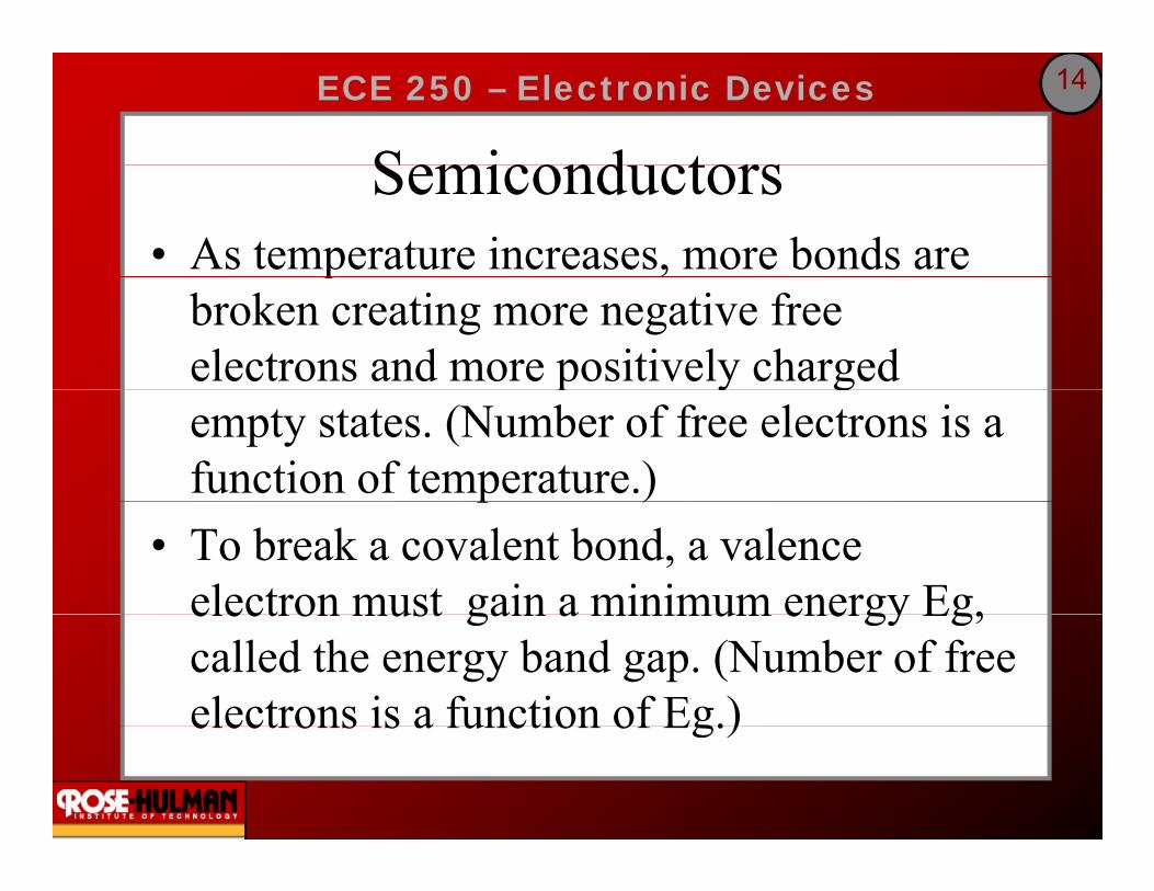
Semicond ctorsSemiconductors• As temperature increases, more bonds are p
broken creating more negative free electrons and more positively charged p y gempty states. (Number of free electrons is a function of temperature.)p )
• To break a covalent bond, a valence electron must gain a minimum energy Eg,electron must gain a minimum energy Eg, called the energy band gap. (Number of free electrons is a function of Eg.)electrons is a function of Eg.)

ECE 250 – Electronic Devices 15
Insulators
• Elements that have a large energy band gap of 3 to 6 eV are insulators because at room temperature, essentially no free electrons exist.
• Note: an eV is an electron volt. It is the amount of energy an electron will gain if itamount of energy an electron will gain if it is accelerated through a 1 volt potential.

ECE 250 – Electronic Devices 16
Electron Volt( )( )llV 19 11060211 −( )( )
( ) joulecoul
voltcouleV19
19
110602.1
110602.11−
−
⎟⎠⎞
⎜⎝⎛×=
×=
( )joules
coulombcoul
1910602.1
110602.1−×=
⎟⎠
⎜⎝
Also, 1 eV = 1.518 ×10⁻²² BTU, but who cares.

ECE 250 – Electronic Devices 17
Conductors
• Elements that have a small energy band gap are conductors.
• These elements have a large number of free electrons at room temperature because theelectrons at room temperature because the electrons need very little energy to escape from their covalent bondsfrom their covalent bonds.

ECE 250 – Electronic Devices 18
Semiconductors
• Semiconductors have a band gap energy of about 1 eV– Silicon = 1.1 eV– GaAs = 1.4 eVGaAs 1.4 eV– Ge = 0.66 eV

ECE 250 – Electronic Devices 19
Empty States
• An electron that has sufficient energy and is adjacent to an empty state may move into j p y ythe empty state, leaving an empty state behind.

ECE 250 – Electronic Devices 20
Si Si Si Si Si Si
Si Si Si Si Si Si
Si Si Si Si Si Si+
This electron can fill the empty
Si Si Si Si Si Sifill the empty
state.
Si Si Si Si Si SiEmpty state originally here.

ECE 250 – Electronic Devices 21
Si Si Si Si Si Si
Si Si Si Si Si Si+
Si Si Si Si Si Si
Si Si Si Si Si SiEmpty state
Si Si Si Si Si Sinow here.

ECE 250 – Electronic Devices 22
Si Si Si Si Si Si
Si Si Si Si Si Si+
Si Si Si Si Si Si
Si Si Si Si Si Si
Si Si Si Si Si Si

ECE 250 – Electronic Devices 23
Si Si Si Si Si Si
Si Si Si Si Si Si
Si Si Si Si Si Si+
Si Si Si Si Si Si
Si Si Si Si Si Si

ECE 250 – Electronic Devices 24
Empty States
• Moving empty states can give the appearance that positive charges move through the material.
• This moving empty state is modeled as a positively charged particle called a hole.
• In semiconductors, two types of “particles” contribute to the current: positively charged holes and negatively charged electrons.

ECE 250 – Electronic Devices 25
Carrier Concentrations
• The concentrations of holes and free electrons are important quantities in the p qbehavior of semiconductors.
• Carrier concentration is given as the numberCarrier concentration is given as the number of particles per unit volume, or
• Carrier concentration = #• Carrier concentration = 3
#cm

ECE 250 – Electronic Devices 26
Intrinsic Semioconductor
• Definition – An intrinsic semiconductor is a single crystal semiconductor with no other g ytypes of atoms in the crystal. – Pure siliconPure silicon– Pure germanium– Pure gallium arsenidePure gallium arsenide.

ECE 250 – Electronic Devices 27
Carrier Concentration
• In an intrinsic semiconductor, the number of holes and free electrons are the same because they are thermally generated.
• If an electron breaks its covalent bond we have one free electron and one hole.
• In an intrinsic semiconductor, the concentration of holes and free electrons are the same.

ECE 250 – Electronic Devices 28
Intrinsic Semiconductorsn
• = the concentration of free electrons in anin
the concentration of free electrons in an intrinsic semiconductor.
• = the concentration of holes in an intrinsic• = the concentration of holes in an intrinsic semiconductor.

ECE 250 – Electronic Devices 29
Intrinsic Carrier Concentration⎟⎞
⎜⎛ − EgBT e p2
3
• B and Eg are determined by the properties
⎟⎠
⎜⎝
=KT
gBTni 2exp2
• B and Eg are determined by the properties of the semiconductor.E b d ( V)• Eg = band gap energy (eV)
• B = material constant
( ) ( ) ⎟⎟
⎠
⎞
⎜⎜
⎝
⎛
233
#
Kcm o( ) ( ) ⎠⎝ ⋅ 2Kcm

ECE 250 – Electronic Devices 30
Intrinsic Carrier Concentration⎟⎞
⎜⎛ − EgBT e p2
3⎟⎠
⎜⎝
=KT
gBTni 2exp2
• T = temperature (ºK)• K = Boltzmann’s constant = 86 2×10⁻⁶ eV/ºK• K = Boltzmann s constant = 86.2×10 6 eV/ K

ECE 250 – Electronic Devices 31
Material Constants⎞⎛Material Eg (eV) B
( ) ( ) ⎟⎟
⎠
⎞
⎜⎜
⎝
⎛
⋅ 233
#
Kcm o
Silicon 1.12 5.23×10¹⁵
Gallium Arsenide
1.4 2.10×10¹⁴
Germanium 0.66 1.66×10¹⁴

ECE 250 – Electronic Devices 32
Important Note:B k li htl diff tBook uses a slightly different
Notation!No o !
⎟⎞
⎜⎛ − Eg3 ⎟
⎠⎞
⎜⎝⎛=
KTEgBTni exp3

ECE 250 – Electronic Devices 33
Book Material Constants
Material Eg (eV) B ( ) ( ) ⎟⎟⎠
⎞⎜⎜⎝
⎛
⋅36
#Kcm o
Silicon 1.12 5.4×1031

ECE 250 – Electronic Devices 34
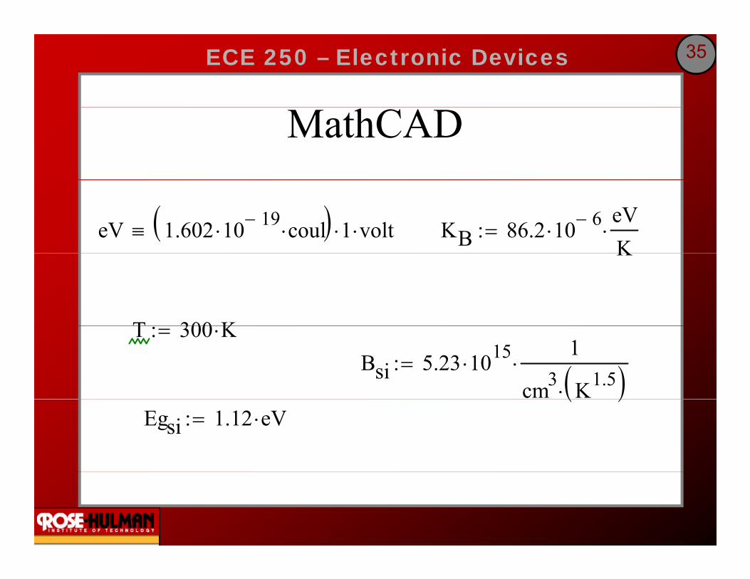
Example
• Find the intrinsic carrier concentration of free electrons and holes in a silicon semiconductor at room temperature.
ECE 250 – Electronic Devices 35
MathCAD
eV 1.602 10 19−⋅ coul⋅( ) 1⋅ volt⋅≡ KB 86.2 10 6−⋅eVK
⋅:=K
T 300 KT 300 K⋅:=Bsi 5.23 1015⋅
1
cm3 K1.5( )⋅⋅:= ( )
Egsi 1.12 eV⋅:=

ECE 250 – Electronic Devices 36
MathCADEg⎛ ⎞
ni Bsi T1.5⋅ expEgsi−
2 KB⋅ T⋅
⎛⎜⎝
⎞⎟⎠
⋅:=⎝ ⎠
ni 1 5 1010×1
=ni 1.5 10×cm3
=
The concentration of silicon atoms in an intrinsic semiconductor is 5×10²² atoms/cm3.
ECE 250 – Electronic Devices 37
Extrinsic Semiconductors
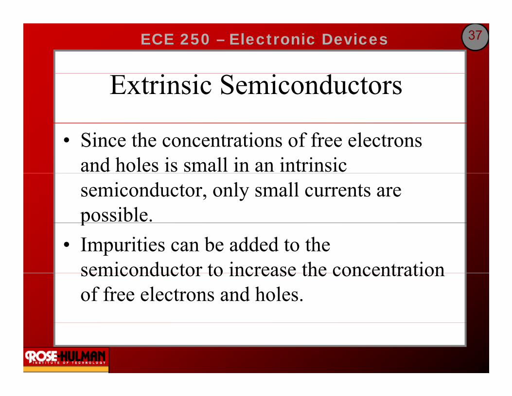
• Since the concentrations of free electrons and holes is small in an intrinsic semiconductor, only small currents are possible.p
• Impurities can be added to the semiconductor to increase the concentrationsemiconductor to increase the concentration of free electrons and holes.

ECE 250 – Electronic Devices 38
Extrinsic Semiconductors
• An impurity would have one less or one more electron in the valance shell than silicon.
• Impurities for group 4 type atoms (silicon)Impurities for group 4 type atoms (silicon) would come from group 3 or group 5 elementselements.

ECE 250 – Electronic Devices 39
Extrinsic Semiconductors
• The most common group 5 elements are phosphorous and arsenic.
• Group 5 elements have 5 electrons in the valence shell.
• Four of the electrons fill the covalent bonds in the silicon crystal structure.
• The 5th electron is loosely bound to the impurity atom and is a free electron at room temperature.

ECE 250 – Electronic Devices 40
Si Si Si Si Si Si
Si Si Si Si Si Si
Si Si P Si Si Si-
Si Si Si Si Si Si
Si Si Si Si Si Si
ECE 250 – Electronic Devices 41
Extrinsic Semiconductors
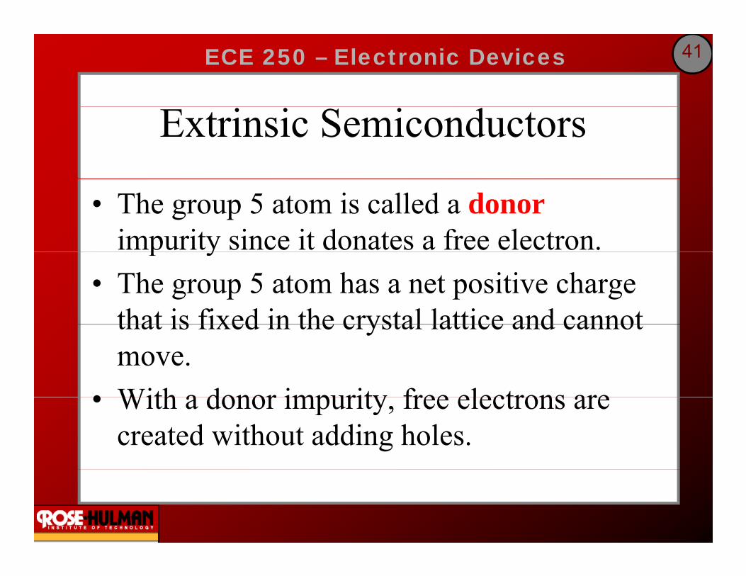
• The group 5 atom is called a donorimpurity since it donates a free electron.p y
• The group 5 atom has a net positive charge that is fixed in the crystal lattice and cannotthat is fixed in the crystal lattice and cannot move.
• With a donor impurity free electrons are• With a donor impurity, free electrons are created without adding holes.

ECE 250 – Electronic Devices 42
Extrinsic Semiconductors
• Adding impurities is called doping.• A semiconductor doped with donorA semiconductor doped with donor
impurities has excess free electron and is called an n-type semiconductorcalled an n type semiconductor.

ECE 250 – Electronic Devices 43
Extrinsic Semiconductors
• The most common group 3 impurity is boron which has 3 valence electrons.
• Since boron has only 3 valence electrons, the boron atom can only bond with three ofthe boron atom can only bond with three of its neighbors leaving one open bond positionposition.

ECE 250 – Electronic Devices 44
Si Si Si Si Si Si
Si Si Si Si Si Si
Si Si B Si Si Si
Si Si Si Si Si Si
Si Si Si Si Si Si

ECE 250 – Electronic Devices 45
Extrinsic Semiconductors
• At room temperature, silicon has free electrons that will fill the open bond pposition, creating a hole in the silicon atom whence it came.
• The boron atom has a net negative charge because of the extra electron but the boronbecause of the extra electron, but the boron atom cannot move.

ECE 250 – Electronic Devices 46
Si Si Si Si Si Si
Si Si Si Si Si Si
Si Si B Si Si Si+
Si Si Si Si Si Si
Si Si Si Si Si Si

ECE 250 – Electronic Devices 47
Extrinsic Semiconductors
• Since boron accepts a valence electron, it is called an acceptor impurity.p p y
• Acceptor impurities create excess holes but do not create free electronsdo not create free electrons.
• A semiconductor doped with an acceptor impurity has extra holes and is called aimpurity has extra holes and is called a p-type semiconductor.

ECE 250 – Electronic Devices 48
Carrier Concentrations
• For any semiconductor in thermal equilibrium nopo=ni
2, whereq opo i ,• no = the concentration of free electrons.• p = the concentration of holes• po = the concentration of holes.• ni = the intrinsic carrier concentration
⎟⎠⎞
⎜⎝⎛ −=
KTEgBTni 2
exp23
⎠⎝ KT2
ECE 250 – Electronic Devices 49
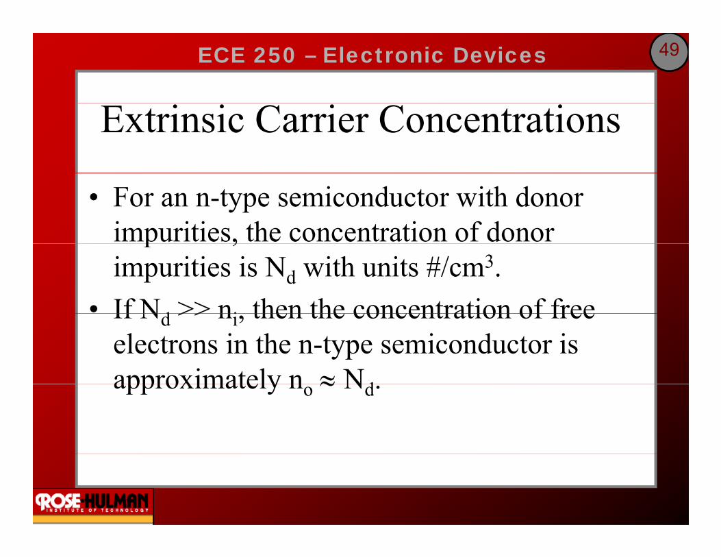
Extrinsic Carrier Concentrations
• For an n-type semiconductor with donor impurities, the concentration of donor p ,impurities is Nd with units #/cm3.
• If Nd >> ni then the concentration of freeIf Nd >> ni, then the concentration of free electrons in the n-type semiconductor is approximately n ≈ Ndapproximately no ≈ Nd.
ECE 250 – Electronic Devices 50
Extrinsic Carrier Concentrations
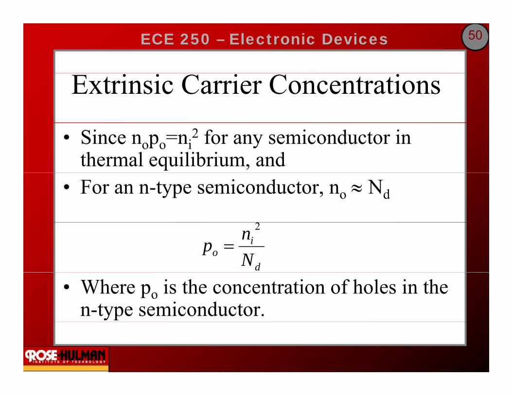
• Since nopo=ni2 for any semiconductor in
thermal equilibrium, and• For an n-type semiconductor, no ≈ Nd
2
d
io N
np2
=
• Where po is the concentration of holes in the n-type semiconductor.

ECE 250 – Electronic Devices 51
Extrinsic Carrier Concentrations
• For a p-type semiconductor with acceptor impurities, the concentration of acceptor p , pimpurities is Na with units #/cm3.
• If N >> ni then the concentration of holesIf Na >> ni, then the concentration of holes in the p-type semiconductor is approximately p ≈ Napproximately po ≈ Na.
ECE 250 – Electronic Devices 52
Extrinsic Carrier Concentrations
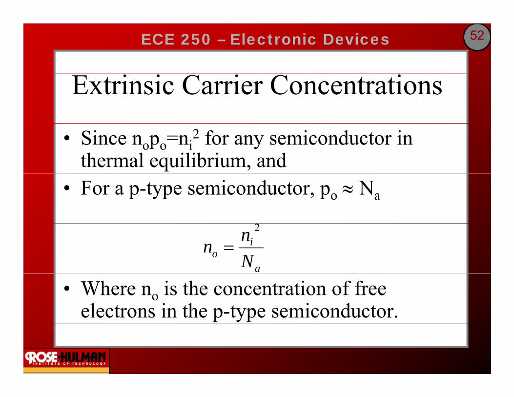
• Since nopo=ni2 for any semiconductor in
thermal equilibrium, and• For a p-type semiconductor, po ≈ Na
2
a
io N
nn2
=
• Where no is the concentration of free electrons in the p-type semiconductor.

ECE 250 – Electronic Devices 53
Current in Semiconductors
• The two processes that cause free electrons and holes to move in a semiconductor are drift and diffusion.
• Drift – the movement of holes and electrons due to an electric field
• Diffusion – the movement of holes and electrons due to variations in concentrations.

ECE 250 – Electronic Devices 54
Drift Current
• Assume that an electric field is applied to to a semiconductor.
• This field acts on holes and electrons.
ECE 250 – Electronic Devices 55
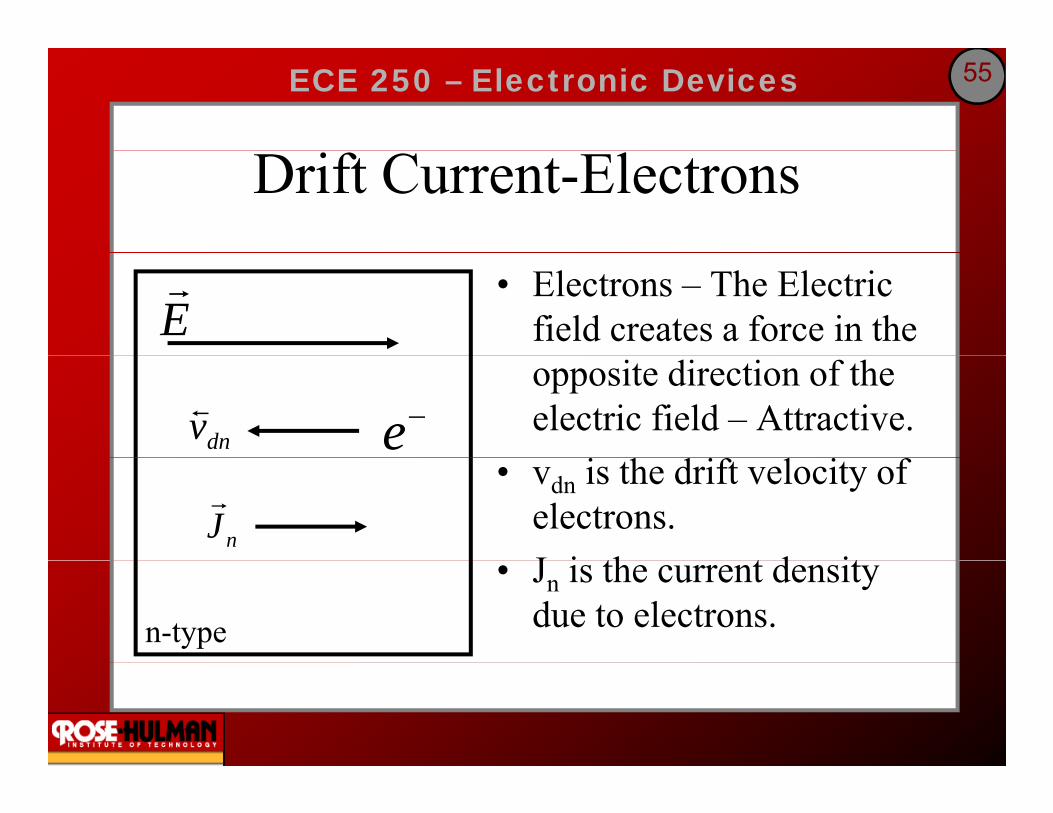
Drift Current-Electrons
• Electrons – The Electric field creates a force in the E
r
opposite direction of the electric field – Attractive.
i h d if l i fdnvs −e
• vdn is the drift velocity of electrons.J i th t d it
nJr
• Jn is the current density due to electrons.n-type

ECE 250 – Electronic Devices 56
Drift Current-Electrons
• The electrons acquire a drift velocity of
Evrs μ
• Where μ is the mobility of electrons with
Ev ndn μ−=
Where μn is the mobility of electrons with units of cm2/(volt-sec).
• The units of vd are cm/secThe units of vdn are cm/sec.• For low-doped silicon, a typical number is μ =1350 cm2/volt-secμn 1350 cm /volt sec.

ECE 250 – Electronic Devices 57
Drift Current-Electronsr
Th i i ( ) i di h h
Ev ndns μ−=
• The minus sign (-) indicates that the electrons move in the opposite direction of th li d l t i fi ldthe applied electric field.

ECE 250 – Electronic Devices 58
Drift Current Density-Electrons
• Current = charge per unit time (coul/sec).• Current density = current flowing through aCurrent density current flowing through a
specific area = amps/unit area = coul/(sec-cm2)cm )

ECE 250 – Electronic Devices 59
Drift Current Density-Electrons
EenenvJ ndnn μ=−=
• e = the charge on an electron = 1.602×10⁻¹⁹
coulombs.• n=concentration of electrons = #/cm3.• en=charge/cm3• en=charge/cm .
223 seccharge
seccmcharge ampcmenvdn === 223 secseccm cmcm⋅

ECE 250 – Electronic Devices 60
Drift Current - Holes
• Holes – The Electric field creates a force in the E
r
same direction of the electric field.
i h d if l i fdpvr+h
• vdp is the drift velocity of holes.J i th t d it
pJr
• Jp is the current density due to holes.n-type

ECE 250 – Electronic Devices 61
Drift Current-Holes• The holes acquire a drift velocity of• The holes acquire a drift velocity of
Evrs μ=
• Where μp is the mobility of holes with units f 2/( lt )
Ev pdp μ=
of cm2/(volt-sec).• The units of vdp are cm/sec.• For low-doped silicon, a typical number is μdp=480 cm2/volt-sec.

ECE 250 – Electronic Devices 62
Mobility - Aside
• Note that μn> μp.
• Electrons are faster than holesElectrons are faster than holes.• P-type and n-type devices operate the same.
However n type devices are fasterHowever, n-type devices are faster.

ECE 250 – Electronic Devices 63
Drift Current Density-Holes
EJ EepepvJ pdpp μ==
• e = the charge on an electron = 1.602×10⁻¹⁹
coulombs.• p=concentration of holes = #/cm3.• ep=charge/cm3• ep=charge/cm .
223 seccharge
seccmcharge ampcmenvdp === 223 secseccm cmcmp ⋅

ECE 250 – Electronic Devices 64
Drift CurrentDrift Current
Er
Er
Er+
Es
dpvr+hJr
dnvs −eJr
pJ nJ
n-type n-type
Drift current due to holes and electrons is in the same direction.

ECE 250 – Electronic Devices 65
Total Drift Current
• Since the hole current and the electron current are in the same direction, the ,currents add.
• The total drift current is:The total drift current is:
rrrEepEenJ pn μμ +=

ECE 250 – Electronic Devices 66
Ohm’s Law
• Another form of Ohm’s law is J=σE• σ is the conductivity of the materialσ is the conductivity of the material.• Noting that
EepEenJ pn
rrrμμ +=
• andEJrv
σ= EJ σ=

ECE 250 – Electronic Devices 67
Conductivity
We can find the conductivity of a semiconductor as
pn epen μμσ +=

ECE 250 – Electronic Devices 68
Diffusion CurrentsDiffusion Currents
(Cover Them)

ECE 250 – Electronic Devices 69
Excess Carriers
• So far we have assumed that the semiconductor is in steady state.y
• Suppose that we shine light on a semiconductorsemiconductor.
• If the photons have sufficient energy, valence electrons may break their covalent bonds andelectrons may break their covalent bonds and create pairs of free electrons and holes.

ECE 250 – Electronic Devices 70
Excess Carriers• These additional holes and electrons are• These additional holes and electrons are
called excess holes (δp) and excess free electrons (δn)electrons (δn).
• When excess holes and free electrons are d h i f h l dcreated, these concentration of holes and
free electrons increase above the thermal ilib i lequilibrium value
n = no+ δn p = po + δpo p po p

ECE 250 – Electronic Devices 71
Excess Carriers
• In steady state, the generation of excess carriers will not cause the carrier concentration to increase indefinitely due to a process called recombination.p
• Electron-Hole Recombination – a free electron combines with a hole and bothelectron combines with a hole and both disappear.

ECE 250 – Electronic Devices 72
Excess Carriers
• Generation – Creates free electrons – hole pairs.p
• Recombination – Eliminates free electrons and holes in pairsand holes in pairs.
• Excess Carrier Lifetime – The mean time over which an excess free electron and holeover which an excess free electron and hole exist before recombination.