ece 4510 introduction to chapter 10 - homepages at wmubazuinb/ece4510/ch10.pdf · ece 4510...
TRANSCRIPT

Material from or based on: The HCS12/9S12: An Introduction to Software & Hardware Interfacing, Thomson Delmar Learning, 2006.
ECE 4510 Introduction to Microprocessors
Chapter 10
Dr. Bradley J. BazuinAssociate Professor
Department of Electrical and Computer EngineeringCollege of Engineering and Applied Sciences

Material from or based on: The HCS12/9S12: An Introduction to Software & Hardware Interfacing, Thomson Delmar Learning, 2006.
ECE 4510 2
Chapter 10
• Serial Peripheral Interface (SPI)– Extended serial string transmission

Material from or based on: The HCS12/9S12: An Introduction to Software & Hardware Interfacing, Thomson Delmar Learning, 2006.
ECE 4510 3
What is Serial Peripheral Interface (SPI)?
• SPI is a synchronous serial protocol proposed by Motorola to be used as standard for interfacing peripheral chips to a microcontroller.
• Devices are classified into the master or slaves.• The SPI protocol uses four wires to carry out the task of data
communication:– MOSI: master out slave in– MISO: master in slave out– SCK: serial clock– SS: slave select
• An SPI data transfer is initiated by the master device. A master is responsible for generating the SCK signal to synchronize the data transfer.
• The SPI protocol is mainly used to interface with shift registers, LED/LCD drivers, phase locked loop chips, memory components with SPI interface, or A/D or D/A converter chips.

Material from or based on: The HCS12/9S12: An Introduction to Software & Hardware Interfacing, Thomson Delmar Learning, 2006.
ECE 4510 4
Memory Addresses
Material from or based on: The HCS12/9S12: An Introduction to Software & Hardware Interfacing, Thomson Delmar Learning, 2006.
ECE 4510 5
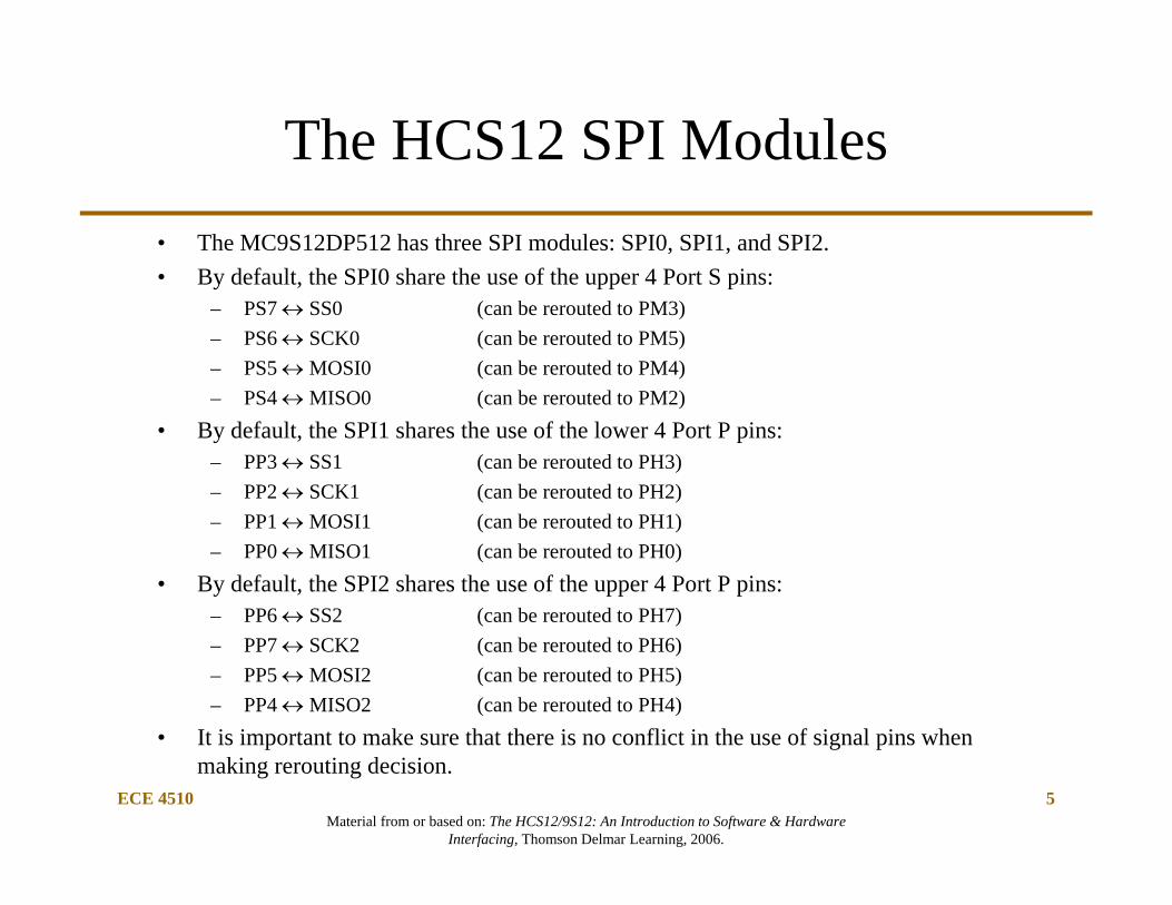
The HCS12 SPI Modules• The MC9S12DP512 has three SPI modules: SPI0, SPI1, and SPI2.• By default, the SPI0 share the use of the upper 4 Port S pins:
– PS7 SS0 (can be rerouted to PM3)– PS6 SCK0 (can be rerouted to PM5)– PS5 MOSI0 (can be rerouted to PM4)– PS4 MISO0 (can be rerouted to PM2)
• By default, the SPI1 shares the use of the lower 4 Port P pins:– PP3 SS1 (can be rerouted to PH3)– PP2 SCK1 (can be rerouted to PH2)– PP1 MOSI1 (can be rerouted to PH1)– PP0 MISO1 (can be rerouted to PH0)
• By default, the SPI2 shares the use of the upper 4 Port P pins:– PP6 SS2 (can be rerouted to PH7)– PP7 SCK2 (can be rerouted to PH6)– PP5 MOSI2 (can be rerouted to PH5)– PP4 MISO2 (can be rerouted to PH4)
• It is important to make sure that there is no conflict in the use of signal pins when making rerouting decision.

Material from or based on: The HCS12/9S12: An Introduction to Software & Hardware Interfacing, Thomson Delmar Learning, 2006.
ECE 4510 6
Adapt9S12DP512 I/O Pins

Material from or based on: The HCS12/9S12: An Introduction to Software & Hardware Interfacing, Thomson Delmar Learning, 2006.
ECE 4510 7
SPI Related Registers (1 of 6)
• The operating parameters of each SPI module are controlled via two control registers: – SPIxCR1: (x = 0, 1, or 2)– SPIxCR2
• The baud rate of SPI transfer is controlled by the SPIxBR register.• The operation status of the SPI operation is recorded in the SPIxSR
register.• The contents of the SPIxCR1, SPIxCR2, SPIxBR, and SPIxSR
registers are illustrated in Figure 10.1 to 10.4, respectively. • The SS pin may be disconnected from SPI by clearing the SSOE bit in
the SPIxCR1 register. After that, it can be used as a general I/O pin.• If the SSOE bit in the SPIxCR1 register is set to 1, then the SS signal
will be asserted to enable the slave device whenever a new SPI transfer is started.
• The equation for setting the SPI baud rate is given in Figure 10.3.

Material from or based on: The HCS12/9S12: An Introduction to Software & Hardware Interfacing, Thomson Delmar Learning, 2006.
ECE 4510 8
7 6 5 4 3 2 1 0
reset: 0 0 0 0 0 1 0 0
MSTR CPOL CPHA SSOESPIE SPE SPTIE LSBFE
Figure 10.1 SPI control register 1 (SPIxCR1, x = 0, 1, or 2)
SPIE: SPI interrupt enable bit 0 = SPI interrupts are disabled 1 = SPI interrupts are enabledSPE: SPI system enable bit 0 = SPI disabled 1 = SPI enabled and pins PS4-PS7 are dedicated to SPI functionSPTIE: SPI transmit interrupt enable 0 = SPTEF interrupt disabled 1 = SPTEF interrupt enabledMSTR: SPI master/slave mode select bit 0 = slave mode 1 = master modeCPOL: SPI clock polarity bit 0 = active high clocks selected; SCK idle low 1 = active low clocks selected, SCK idle highCPHA: SPI clock phase bit 0 = The first SCK edge is issued one-half cycle into the 8-cycle transfer operation. 1 = The SCK edge is issued at the beginning of the 8-cycle transfer operation.SSOE: slave select output enable bit The SS output feature is enabled only in master mode by asserting the SSOE bit and the MODFEN bit of the SPIxCR2 register.LSBF: SPI least-significant-bit first enable bit 0 = data is transferred most-significant bit first 1 = data is transferred least-significant bit first
SPI Related Registers (2 of 6)

Material from or based on: The HCS12/9S12: An Introduction to Software & Hardware Interfacing, Thomson Delmar Learning, 2006.
ECE 4510 9
7 6 5 4 3 2 1 0
reset: 0 0 0 0 1 0 0 0
MODFEN BIDIROE 0 SPSWAI0 0 0 SPC0
Figure 10.2 SPI control register 2 (SPIxCR2, x = 0, 1, or 2)
MODFEN: Mode fault enable bit 0 = Disable the MODF error 1 = Enable settinig the MODF errorBIDIROE: Output enable in the bidirectional mode of operation 0 = Output buffer disabled 1 = Output buffer enabledSPSWAI: SPI stop in wait mode 0 = SPI clock operates normally in stop mode 1 = Stop SPI clock generation in Wait modeSPC0: Serial pin control bit 0 With the MSTR bit in the SPIxCR1 register, this bit enables bidirectional pin configuration as shown in Table 10.1.
SPI Related Registers (3 of 6)

Material from or based on: The HCS12/9S12: An Introduction to Software & Hardware Interfacing, Thomson Delmar Learning, 2006.
ECE 4510 10
MODFEN SSOE Master Mode Slave mode
0011
0101
SS not used by SPISS not used by SPI
SS input with MODF featureSS output
SS inputSS inputSS inputSS input
Table 10.1 SS input/output selection
SPI Related Registers (4 of 6)

Material from or based on: The HCS12/9S12: An Introduction to Software & Hardware Interfacing, Thomson Delmar Learning, 2006.
ECE 4510 11
7 6 5 4 3 2 1 0
reset: 0 0 0 0 0 0 0 0
SPPR0 0 SPR2 SPR10 SPPR2 SPPR1 SPR0
Figure 10.3 SPI baud rate register (SPIxBR, x = 0, 1, or 2)
SPPR2~SPPR0: SPI baud rate preselection bitsSPR2~SPR0: SPI baud rate selection bits
BaudRateDivisor = (SPPR + 1) 2(SPR + 1)
Baud Rate = Bus Clock BaudRateDivisor
7 6 5 4 3 2 1 0
reset: 0 0 1 0 0 0 0 0
MODF 0 0 0SPIF SPTEF0 0
Figure 10.4 SPI status register (SPIxSR)
SPIF: SPI interrupt request bit SPIF is set after the eight SCK cycles in a data transfer, and it is cleared by reading the SP0SR register (with SPIF set) followed by a read access to the SPI data register. 0 = transfer not yet complete 1 = new data copied to SPIxDRSPTEF: SPI data register empty interrupt flag 0 = SPI data register not empty 1 = SPI data register emptyMODF: mode error interrupt status flag 0 = mode fault has not occurred 1 = mode fault has occurred
SPI Related Registers (5 of 6)

Material from or based on: The HCS12/9S12: An Introduction to Software & Hardware Interfacing, Thomson Delmar Learning, 2006.
ECE 4510 12
SPI Related Registers (6 of 6)
• Example 10.1 Give a value to be loaded to the SPIxBR register to set the baud rate to 2 MHz for a 24 MHz bus clock.
• Solution: 24 MHz 2 MHz = 12. One possibility is to set SPPR2-SPPR0 and SPR2-SPR0 to 010 and 001, respectively. The value to be loaded into the SPIxBR register is $21.
• Example 10.2 What is the highest possible baud rate for the SPI with 24 MHz bus clock?
• Solution: The highest SPI baud rate occurs when both the SPPR2-SPPR0 and SPR2-SPR0 are 000. In this case the baud rate is 24 MH 2 = 12 MHz.

Material from or based on: The HCS12/9S12: An Introduction to Software & Hardware Interfacing, Thomson Delmar Learning, 2006.
ECE 4510 13
SPI Transmission Format (1 of 3)
• The data bits can be shifted on the rising or the falling edge of the SCK clock.
• Since the SCK can be idle high or idle low, there are four possible combinations as shown in Figure 10.5 and 10.6.
• To shift data bits on the rising edge, set CPOL-CPHA to 00 or 11.
• To shift data bits on the falling edge, set CPOL-CPHA to 01 or 10.
• Data byte can be shifted in and out most significant bit first or least significant bit first.

Material from or based on: The HCS12/9S12: An Introduction to Software & Hardware Interfacing, Thomson Delmar Learning, 2006.
ECE 4510 14
SS (O)master only
SS (I)
SCK (CPOL = 0)
SCK (CPOL = 1)Sample I
MOSI/MISO
Change OMOSI Pin
Change OMISO Pin
tT tI tLMinimum 1/2 SCK
for tT, tI, tL
tL
MSB first (LSBF = 0)LSB first (LSBF = 1)
MSBLSB
Bit 6Bit 1
Bit 5Bit 2
Bit 4Bit 3
Bit 3Bit 4
Bit 2Bit 5
Bit 1Bit 6
LSBMSB
Begin EndTransfer
Figure 10.5 SPI Clock format 0 (CPHA = 0)
SPI Transmission Format (2 of 3)

Material from or based on: The HCS12/9S12: An Introduction to Software & Hardware Interfacing, Thomson Delmar Learning, 2006.
ECE 4510 15
SS (O)master only
SS (I)
SCK (CPOL = 0)
SCK (CPOL = 1)Sample I
MOSI/MISO
Change OMOSI Pin
Change OMISO Pin
tT tI tLMinimum 1/2SCK for tT, tI, tL
tLMSB first (LSBF = 0)LSB first (LSBF = 1)
MSBLSB
Bit 6Bit 1
Bit 5Bit 2
Bit 4Bit 3
Bit 3Bit 4
Bit 2Bit 5
Bit 1Bit 6
LSBMSB
Begin EndTransfer
Figure 10.6 SPI Clock format 1 (CPHA = 1)
SPI Transmission Format (3 of 3)

Material from or based on: The HCS12/9S12: An Introduction to Software & Hardware Interfacing, Thomson Delmar Learning, 2006.
ECE 4510 16
Bidirectional Mode (MOMI or SISO)• A mode that uses only one data pin to shift data in and out.• This mode is provided to deal with peripheral devices with only one data
pin.• Either the MOSI pin or the MISO pin can be used as the bidirectional pin.• When the SPI is configured to the master mode (MSTR bit = 1), the MOSI
pin is used in data transmission and becomes the MOMI pin.• When the SPI is configured to the slave mode (MSTR bit = 0), the MISO
pin is used in data transmission and becomes the SISO pin.• The direction of each serial pin depends on the BIDIROE bit of the
SPIxCR2 register.• The pin configuration for MOSI and MISO are illustrated in Figure 10.7.• To read data from the peripheral device, clear the BIDIROE bit to 0.• To output data to the peripheral device, set the BIDIROE bit to 1.• The use of the this mode is illustrated in exercise problem 10.8.

Material from or based on: The HCS12/9S12: An Introduction to Software & Hardware Interfacing, Thomson Delmar Learning, 2006.
ECE 4510 17
Figure 10.7 Normal mode and bidirectional mode
Serial Out
SPI
Serial In
MOSI
MISO
When SPE = 1
NormalMode
SPC0 = 0
Master modeMSTR = 1
Serial Out
SPI
Serial In
MOMI
BIDIROE
Serial Out
SPI
Serial In
SISO
BIDIROE
Serial Out
SPISerial In MOSI
MISO
Slave ModeMSTR = 0
SWOM enables open-drain output SWOM enables open-drain output
Bi-directionalmode
SPC0 = 1
Normal and Bidirectional Mode

Material from or based on: The HCS12/9S12: An Introduction to Software & Hardware Interfacing, Thomson Delmar Learning, 2006.
ECE 4510 18
Mode Fault Error
• If the SSx signal goes low while the SPIx is configured as a master, it indicates a system error where more than one master may be trying to drive the MOSIx and SCKx pins simultaneously.
• The MODF bit in the SPIxSR register will be set to 1 when mode fault condition occurs.
• When mode fault occurs, the MSTR bit will be cleared to 0 and the output enable for the MOSIx and SCKx pins will be deasserted.

Material from or based on: The HCS12/9S12: An Introduction to Software & Hardware Interfacing, Thomson Delmar Learning, 2006.
ECE 4510 19
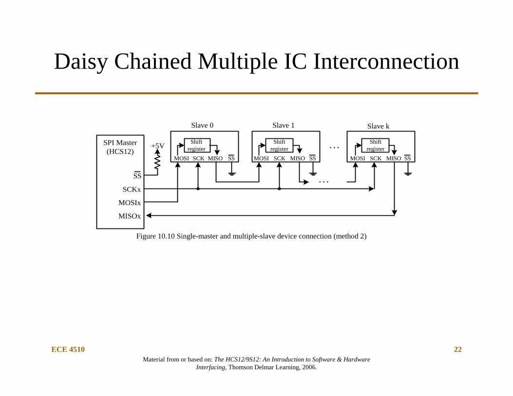
SPI Circuit Connection
• In an SPI system, one device is configured as a master. Other devices are configured as slaves.
• The circuit connection for a single-slave system is shown in Figure 10.8.
• A multi-slave system may have two different connection methods as illustrated in Figure 10.9 and 10.10.
• In Figure 10.9, the master can exchange data with each individual slave without affecting other slaves.
• In Figure 10.10, all the slaves are configured into a larger ring. A data transmission with certain slaves will go through other slaves.

Material from or based on: The HCS12/9S12: An Introduction to Software & Hardware Interfacing, Thomson Delmar Learning, 2006.
ECE 4510 20
Shift register
Shift register
Baud RateGenerator
VDD
MISO
MOSI
SCK SCK
MOSI
MISO
SSSS
Master SPI Slave SPI
Figure 10.8 Master/slave transfer block diagram
Single IC Interconnection

Material from or based on: The HCS12/9S12: An Introduction to Software & Hardware Interfacing, Thomson Delmar Learning, 2006.
ECE 4510 21
SS
+5V
MOSI SCK MISO SS
Shiftregister
MOSI SCK MISO SS
Shiftregister
MOSI SCK MISO
Shiftregister
SS
SPI Master(HCS12)
SCKx
MOSIx
MISOx
PP0
PP1
PPk
.
.
.
.
.
.
. . .
Slave 0 Slave 1 Slave k
Figure 10.9 Single-master and multiple-slave device connection (method 1)
SS Multiple IC Interconnection
Material from or based on: The HCS12/9S12: An Introduction to Software & Hardware Interfacing, Thomson Delmar Learning, 2006.
ECE 4510 22
Daisy Chained Multiple IC Interconnection
SS
+5VMOSI SCK MISO SS
Shiftregister
MOSI SCK MISO SS
Shiftregister
MOSI SCK MISO
Shiftregister
SS
SPI Master(HCS12)
SCKx
MOSIx
MISOx
. . .
Slave 0 Slave 1 Slave k
Figure 10.10 Single-master and multiple-slave device connection (method 2)
. . .

Material from or based on: The HCS12/9S12: An Introduction to Software & Hardware Interfacing, Thomson Delmar Learning, 2006.
ECE 4510 23
Example 10.3
• Example 10.3 Configure the SPI0 to operate with the following setting assuming that Eclock is 24 MHz:– 6 MHz baud rate– Enable SPI0 to master mode– SCK0 pin idle low with data shifted on the rising edge of SCK– Transfer data most significant bit first and disable interrupt– Disable SS0 function– Stop SPI in Wait mode– Normal SPI operation (not bidirectional mode)

Material from or based on: The HCS12/9S12: An Introduction to Software & Hardware Interfacing, Thomson Delmar Learning, 2006.
ECE 4510 24
movb #$10, SPI0BR ; set baud rate to 6 MHzmovb #$50, SPI0CR1 ; disable interrupt, enable SPI, SCK idle low, data
; latched on rising edge, data transferred msb firstmovb #$02, SPI0CR2 ; disable bidirectional mode, stop SPI in wait modemovb #0, WOMS ; enable Port S pull-up
Example 10.3
• Solution: fE / baud rate = 24 MHz/6 MHz = 4. We need to set SPPR2-SPPR0 and SPR2-SPR0 to 001 and 000, respectively. Write the value $10 into the SPI0BR register.– The following instruction sequence will configure the SPI0 as desired:

Material from or based on: The HCS12/9S12: An Introduction to Software & Hardware Interfacing, Thomson Delmar Learning, 2006.
ECE 4510 25
SPI Desirable Utility Functions
• The following operations are common in many applications and should be made into library functions to be called by many SPI applications:– Send a character to SPI putcspix (x = 0, 1, or 2)– Send a string to SPI putsspix (x = 0, 1, or 2)– Read a character from SPI getcspix (x = 0, 1, or 2)– Read a string from SPI getsspix (x = 0, 1, or 2)
Material from or based on: The HCS12/9S12: An Introduction to Software & Hardware Interfacing, Thomson Delmar Learning, 2006.
ECE 4510 26
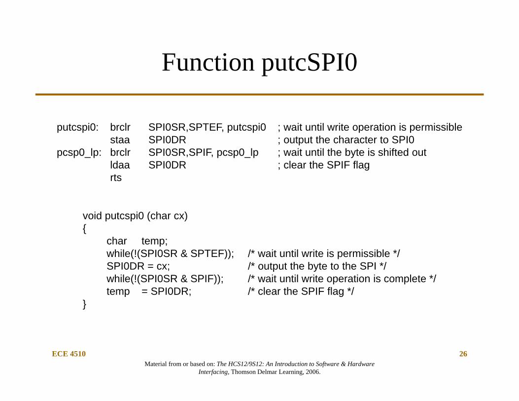
putcspi0: brclr SPI0SR,SPTEF, putcspi0 ; wait until write operation is permissiblestaa SPI0DR ; output the character to SPI0
pcsp0_lp: brclr SPI0SR,SPIF, pcsp0_lp ; wait until the byte is shifted outldaa SPI0DR ; clear the SPIF flagrts
void putcspi0 (char cx){
char temp;while(!(SPI0SR & SPTEF)); /* wait until write is permissible */SPI0DR = cx; /* output the byte to the SPI */while(!(SPI0SR & SPIF)); /* wait until write operation is complete */temp = SPI0DR; /* clear the SPIF flag */
}
Function putcSPI0

Material from or based on: The HCS12/9S12: An Introduction to Software & Hardware Interfacing, Thomson Delmar Learning, 2006.
ECE 4510 27
; the string to be output is pointed to by Xputsspi0: ldaa 1,x+ ; get one byte to be output to SPI port
beq doneps0 ; reach the end of the string?jsr putcspi0 ; call subroutine to output the bytebra putsspi0 ; continue to output
doneps0: rts
void putsspi0(char *ptr){
while(*ptr) { /* continue until all characters have been output */putcspi0(*ptr);ptr++;
}}
Function putsSPI0

Material from or based on: The HCS12/9S12: An Introduction to Software & Hardware Interfacing, Thomson Delmar Learning, 2006.
ECE 4510 28
; This function reads a character from SPI0 and returns it in accumulator A
getcspi0: brclr SPI0SR,SPTEF, getcspi0 ; wait until write operation is permissiblestaa SPI0DR ; trigger eight clock pulses for SPI transfer
gcsp0_lp: brclr SPI0SR,SPIF, gcsp0_lp ; wait until a byte has been shifted inldaa SPI0DR ; return the byte in A and clear the SPIF flagrts
char getcspi0(void){
while(!(SPI0SR & SPTEF)); /* wait until write is permissible */SPI0DR = 0x00; /* trigger 8 SCK pulses to shift in data */while(!(SPI0SR & SPIF)); /* wait until a byte has been shifted in */return SPI0DR; /* return the character */
}
Function getcSPI0

Material from or based on: The HCS12/9S12: An Introduction to Software & Hardware Interfacing, Thomson Delmar Learning, 2006.
ECE 4510 29
; This function reads a string from the SPI and store it in a buffer pointed to by X; The number of bytes to be read in passed in accumulator B
getsspi0: tstb ; check the byte countbeq donegs0 ; return when byte count is zerojsr getcspi0 ; call subroutine to read a bytestaa 1,x+ ; save the returned byte in the bufferdecb ; decrement the byte countbra getsspi0
donegs0: clr 0,x ; terminate the string with a NULL characterrts
void getsspi0(char *ptr, char count){
while(count) { /* continue while byte count is nonzero */*ptr++ = getcspi0(); /* get a byte and save it in buffer */count--;
}*ptr = 0; /* terminate the string with a NULL */
}
Function getsSPI0

Material from or based on: The HCS12/9S12: An Introduction to Software & Hardware Interfacing, Thomson Delmar Learning, 2006.
ECE 4510 30
Shiftregister
QAQBQCQDQEQFQGQH
Latch
SQH
15
13
1234567
912
10
11
DS 14
Reset
LC
OE
SC
Figure 10.11 The 74HC595 block diagram and pin assignment
VCC = Pin 16GND = Pin 8
SPI ICs: The HC595 Shift Register
• The HC595 consists of an 8-bit shift register and a D-type latch with three-state parallel output.
• The shift register provides parallel data to the latch.• The maximum data shift rate is 100 MHz (Philips part).

Material from or based on: The HCS12/9S12: An Introduction to Software & Hardware Interfacing, Thomson Delmar Learning, 2006.
ECE 4510 31
Signal Pins of the HC595
• DS: serial data input• SC: shift clock. A low-to-high transition on this pin causes
the data at the serial input pin to be shifted into the 8-bit shift register.
• Reset: A low on this pin resets the shift register portion of this device.
• LC: latch clock. A low-to-high transition on this pin loads the contents of the shift register into the output latch.
• OE: output enable. A low on this pin allows the data from the latches to be presented at the outputs.
• QA to QH: tri-state latch output• SQH: the output of the eight stage of the shift register

Material from or based on: The HCS12/9S12: An Introduction to Software & Hardware Interfacing, Thomson Delmar Learning, 2006.
ECE 4510 32
Applications of the HC595 (1 of 2)
• The HC595 is often used to add parallel ports to the microcontroller.
• Both the connection methods shown in Figure 10.9 and 10.10 can be used to add parallel ports to the MCU.

Material from or based on: The HCS12/9S12: An Introduction to Software & Hardware Interfacing, Thomson Delmar Learning, 2006.
ECE 4510 33
ab
g
Figure 10.12 Two 74HC595s together drive eight seven-segment displays
. . .. . .
. . .
ab
g
.
.
.
commoncathode
commoncathode
ab
g
I MA
X =
70
mA
.
.
.
R
R
R 2N2222
2N2222
2N2222
300
300
#7 #6 #0
HCS12
MOSI0
SCK0
.
.
.
SC
SC
DS
DS
SQHLC
LC
5V
5V
QGQF
QA
.
.
.
74HC595
74HC595
reset
resetQH
QG
QA
.
.
.OE
OE
commoncathode
PK7
Example 10.5
• Example 10.5 Describe how to use two 74HC595s to drive eight common cathode seven-segment displays assuming that the E clock frequency of the HCS12 is 24 MHz.
• Solution: Use the circuit in figure 10.12 to connect two 74HC595s to the HCS12.

Material from or based on: The HCS12/9S12: An Introduction to Software & Hardware Interfacing, Thomson Delmar Learning, 2006.
ECE 4510 34
#include “c:\miniide\hcs12.inc".org $1000dispTab: .byte $80,$7F,$40,$70,$20,$5F,$10,$5B
.byte $08,$33,$04,$79,$02,$6D,$01,$30icnt: .blkb 1 ; loop count.text_main::
lds #$3C00 ; set up stack pointerbset DDRK,$80 ; configure the PK7 pin for outputjsr openspi0 ; configure SPI0
forever: ldx #dispTab ; use X as a pointer to the tablemovb #8,icnt ; set loop count to 8
loop: ldaa 1,x+ ; send the digit select byte to the 74HC595jsr putcspi0 ; "ldaa 1,x+ ; send segment pattern to 74HC595jsr putcspi0 ; "bclr PTK,BIT7 ; transfer data from shift register to outputbset PTK,BIT7 ; latchldy #1 ; display the digit for one msjsr delayby1ms ; "dec icnt ; bne loop ; if not reach digit 1, then nextbra forever ; start from the start of the table
ASM Program to display 87654321 on display #7 to #0 (1 of 2)

Material from or based on: The HCS12/9S12: An Introduction to Software & Hardware Interfacing, Thomson Delmar Learning, 2006.
ECE 4510 35
openspi0: movb #0,SPI0BR ; set baud rate to 12 MHzmovb #$50,SPI0CR1 ; disable interrupt, enable SPI, SCK idle low,
; latch data on rising edge, transfer data msb firstmovb #$02,SPI0CR2 ; disable bidirectional mode, stop SPI in wait modemovb #0,WOMS ; enable Port S pull-uprts
#include "c:\miniide\delay.asm"#include "c:\miniide\spi0util.asm"
ASM Program to display 87654321 on display #7 to #0 (2 of 2)

Material from or based on: The HCS12/9S12: An Introduction to Software & Hardware Interfacing, Thomson Delmar Learning, 2006.
ECE 4510 36
#include “c:\egnu091\include\hcs12.h”#include “c:\egnu091\include\spi0util.c”#include “c:\egnu091\include\delay.c”void openspi0(void);void main (void){
unsigned char disp_tab[8][2] = {{0x80,0x7F},{0x40,0x70},{0x20,0x5F},{0x10,0x5B},{0x08,0x33},{0x04,0x79},{0x02,0x6D},{0x01,0x30}};
char i;openspi0(); /* configure the SPI0 module */DDRK |= BIT7; /* configure pin PK7 as output */while(1) {
for (i = 0; i < 8; i++) {putcspi0(disp_tab[i][0]); /* send out digit select value */putcspi0(disp_tab[i][1]); /* send out segment pattern */PTK &= ~BIT7; /* transfer values to latches of 74HC595s */PTK |= BIT7; /* " */delayby1ms(1); /* display a digit for 1 ms */
}}
}
C Program

Material from or based on: The HCS12/9S12: An Introduction to Software & Hardware Interfacing, Thomson Delmar Learning, 2006.
ECE 4510 37
NC
CE
SCK
GND
VDD
NC
SDI
SDO
TC72
Internaldiode
temperaturesensor
10-bitsigma Delta
A/Dconverter
temperatureregister
ManufacturerID register
ControlRegister
SerialPort
Interface
CESCKSDOSDI
GND
VDDTC72
Figure 10.13 TC72 pin assignment and functional block diagram
1
2
3
4 5
6
7
8
The TC72 Digital Thermometer• 10-bit resolution and SPI interface• Pin assignment and block diagram shown in Figure 10.13.• Capable of reading temperature from -55oC to 125oC.• Can be used in continuous temperature conversion or one-shot conversion mode. • Has internal clock generator to control the automatic temperature conversion sequence

Material from or based on: The HCS12/9S12: An Introduction to Software & Hardware Interfacing, Thomson Delmar Learning, 2006.
ECE 4510 38
Binaryhigh byte/low byte
0010 0001/0100 00000100 1010/1000 00000001 1010/1100 00000000 0001/1000 00000000 0000/0000 00001111 1111/1000 00001111 0010/1100 00001110 0111/0000 00001100 1001/0100 0000
Hex
21404A801AC001800000FF80F2C0E700C900
Temperature
33.25 oC74.5oC
26.75 oC1.5oC0oC
-0.5oC-13.25oC
-24oC-55oC
Table 10.3 TC72 Temperature output data
Temperature Data Format• Temperature is represented by a 10-bit two’s complement word with a resolution of
0.25oC per least significant bit.• The converter is scaled from -128oC to +127oC with 0oC represented as 0x0000.• The temperature value is stored in two 8-bit registers.• Whenever the most significant bit is 1, the temperature is negative.• A sample of temperature reading is shown.

Material from or based on: The HCS12/9S12: An Introduction to Software & Hardware Interfacing, Thomson Delmar Learning, 2006.
ECE 4510 39
Register Readaddress
Writeaddress
Bit7
Bit6
Bit5
Bit4
Bit3
Bit2
Bit1
Bit0
Value onPOR/BOR
ControlLSB temperature
MSB temperatureManufacturer ID
0x000x010x020x03
0x80N/AN/AN/A
0T1T90
0T0T81
00
T70
OS0
T61
00
T50
00
T41
00
T30
SHDN0
T20
0x050x000x000x54
Table 10.4 Register for TC72
Note. 1. OS is One-Shot 2. SHDN is Shutdown
TC72’s Serial Interface• The CE input to the TC72 must be asserted (high) to enable SPI transfer.• Data can be shifted on the rising edge or the falling edge depending on the idle polarity of the SCK
source.• Data transfer to and from the TC72 consists of one address byte followed by one or multiple data (2
to 4) bytes. • The TC72 registers and their addresses are shown in Table 10.4. • The most significant bit of the address byte determines whether a read (A7 = 0) or a write (A7 = 1)
operation will occur. • A multiple byte read operation will start from high address toward lower addresses. • The user can send in the temperature result high byte address and read the temperature result high
byte, low byte, and the control registers.

Material from or based on: The HCS12/9S12: An Introduction to Software & Hardware Interfacing, Thomson Delmar Learning, 2006.
ECE 4510 40
Procedure for Reading Temperature (1 of 2)
• Step 1– Pull the CE pin high to enable SPI transfer.
• Step 2– Send the temperature result high byte read address (0x02) to the TC72.
Wait until the SPI transfer is complete.• Step 3
– Read the temperature result high byte. The user needs to write a dummy byte into the SPI data register to trigger eight clock pulses.
• Step 4– Read the temperature result low byte. Again, the user needs to write a
dummy byte into the SPI data register to trigger eight clock pulses.• Step 5
– Pull CE pin to low so that a new transfer can be started.

Material from or based on: The HCS12/9S12: An Introduction to Software & Hardware Interfacing, Thomson Delmar Learning, 2006.
ECE 4510 41
CE
SCK
SDI
SDO High Z
A7
A6
A5
A4
A3
A2
A1
A0
D7
D6
D5
D4
D3
D2
D1
D0
1 2 3 4 5 6 7 8 9 1 0 1 1 1 2 1 3 1 4 1 5 1 6
A7 = 0
Figure 10.15b Single data byte read operation
high Z
CE
SCK
D7
D0
D7
D0
D7
D0SDO
Write operation
Read operation
A7
A0
Address byte = 0x02
SDI
Figure 10.15c SPI multiple data byte transfer
Procedure for Reading Temperature (2 of 2)

Material from or based on: The HCS12/9S12: An Introduction to Software & Hardware Interfacing, Thomson Delmar Learning, 2006.
ECE 4510 42
Operation mode
Continuous temperature conversionShutdownContinuous temperature conversionOne-shot
One-Shot bit
0011
0101
Shutdown bit
Table 10.5 Control register temperature conversion mode selection
Control Register
• The control register is used to select the shutdown, continuous, or one-shot conversion operating mode.
• The temperature conversion mode selection logic is shown in Table 10.5.• At power up, the SHDN bit is 1. Thus the TC72 is in the shutdown mode.• If the SHDN bit is 0, the TC72 will perform a temperature conversion
approximately every 150 ms.• A temperature conversion will be initiated by a write operation into the control
register to select the continuous mode or one-shot mode. • A typical circuit connection between the TC72 and the HCS12 is shown in
Figure 10.16.

Material from or based on: The HCS12/9S12: An Introduction to Software & Hardware Interfacing, Thomson Delmar Learning, 2006.
ECE 4510 43
CE
SCK
SDO
SDI
PK7
SCK0
MISO0
MOSI0
HCS12 MCUTC72
VDD VDD
GND
0.1F
Figure 10.16 Circuit connection between the TC72 and the HCS12
Example 10.6: Reading Temp.
• Write a C program to read the temperature every 200 ms. Convert the temperature to a string so that it can be displayed in an appropriate output device. A pointer to hold the string will be passed to this function. The bus clock is 24 MHz.

Material from or based on: The HCS12/9S12: An Introduction to Software & Hardware Interfacing, Thomson Delmar Learning, 2006.
ECE 4510 44
#include “c:\egnu091\include\hcs12.h”#include “c:\egnu091\include\spi0util.c”#include “c:\egnu091\include\delay.c”#include “c:\egnu091\include\convert.c”void read_temp (char *ptr); void openspi0(void);char buf[10];void main (void){
DDRM |= BIT1; /* configure the PM1 pin for output */openspi0(); /* configure SPI0 module */read_temp(&buf[0]);
}void openspi0(void){
SPI0BR = 0x10; /* set baud rate to 6 MHz */SPI0CR1 = 0x50; /* enable SPI0 to master mode, select rising edge to
shift data in and out */SPI0CR2 = 0x02; /* select normal mode and stop SPI in wait mode */WOMS = 0x00; /* enable Port S pull-up */
}
C Code (1 of 4)

Material from or based on: The HCS12/9S12: An Introduction to Software & Hardware Interfacing, Thomson Delmar Learning, 2006.
ECE 4510 45
void read_temp (char *ptr){
char hi_byte, lo_byte, temp, *bptr;unsigned int result;bptr = ptr;PTM |= BIT1; /* enable TC72 data transfer */putcspi0(0x80); /* send out TC72 control register write address */putcspi0(0x11); /* perform one shot conversion */PTM &= ~BIT1; /* disable TC72 data transfer */delayby100ms(2); /* wait until temperature conversion is complete */PTM |= BIT1; /* enable TC72 data transfer */putcspi0(0x02); /* send MSB temperature read address */hi_byte = getcspi0(); /* read the temperature high byte */lo_byte = getcspi0(); /* save temperature low byte and clear SPIF */PTM &= ~BIT1; /* disable TC72 data transfer */
lo_byte &= 0xC0; /* make sure the lower 6 bits are 0s */result = (int) hi_byte * 256 + (int) lo_byte;if (hi_byte & 0x80) { /* temperature is negative */
result = ~result + 1; /* take the two' complement of result */result >>= 6;
C Code (2 of 4)

Material from or based on: The HCS12/9S12: An Introduction to Software & Hardware Interfacing, Thomson Delmar Learning, 2006.
ECE 4510 46
temp = result & 0x0003; /* place the lowest two bits in temp */result >>= 2; /* get rid of fractional part */*ptr++ = 0x2D; /* store the minus sign */int2alpha(result, ptr);
}else { /* temperature is positive */
result >>= 6;temp = result & 0x0003; /* save fractional part */result >>= 2; /* get rid of fractional part */int2alpha(result, ptr); /* convert to ASCII string */
}while(*bptr){ /* search the end of the string */
bptr++;};switch (temp){ /* add fractional digits to the temperature */
case 0:break;
case 1: /* fractional part is .25 */*bptr++ = 0x2E; /* add decimal point */*bptr++ = 0x32;*bptr++ = 0x35;*bptr = '\0';break;
C Code (3 of 4)

Material from or based on: The HCS12/9S12: An Introduction to Software & Hardware Interfacing, Thomson Delmar Learning, 2006.
ECE 4510 47
case 2: /* fractional part is .5 */*bptr++ = 0x2E; /* add decimal point */*bptr++ = 0x35;*bptr = '\0';break;
case 3: /* fractional part is .75 */*bptr++ = 0x2E; /* add decimal point */*bptr++ = 0x37;*bptr++ = 0x35;*bptr = '\0';break;
default:break;
}}
C Code (4 of 4)