ece53a rlc circuits w. ku 11/29/2007 1.first order linear time invariant circuits 2.second order lti...
Post on 21-Dec-2015
229 views
TRANSCRIPT
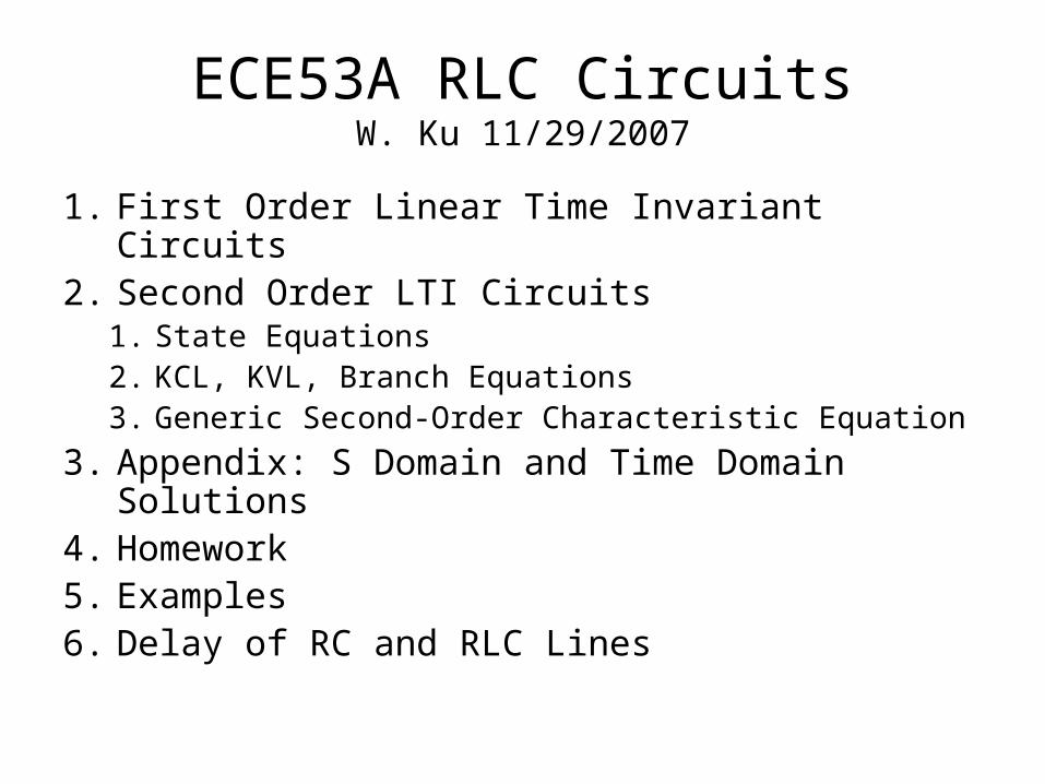
ECE53A RLC CircuitsW. Ku 11/29/2007
1. First Order Linear Time Invariant Circuits2. Second Order LTI Circuits
1. State Equations2. KCL, KVL, Branch Equations3. Generic Second-Order Characteristic Equation
3. Appendix: S Domain and Time Domain Solutions
4. Homework5. Examples6. Delay of RC and RLC Lines
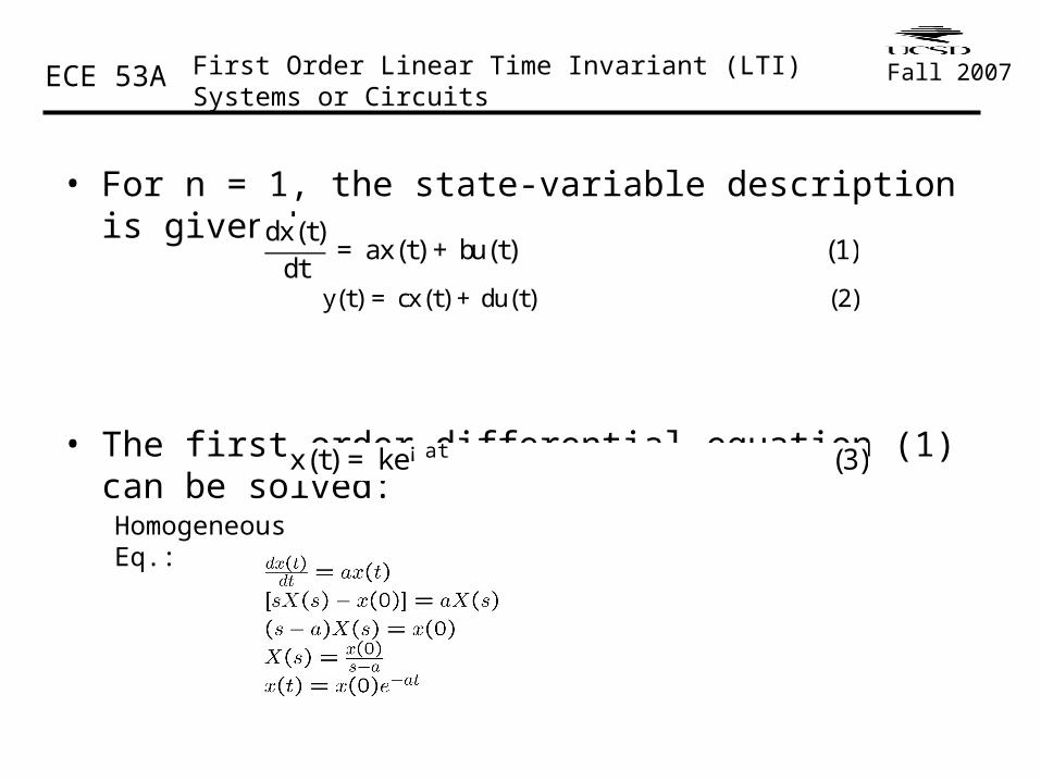
• For n = 1, the state-variable description is given by
• The first-order differential equation (1) can be solved:
ECE 53A First Order Linear Time Invariant (LTI) Systems or Circuits Fall 2007
dx(t)dt
= ax(t) +bu(t) (1)
y(t) = cx(t) +du(t) (2)
x(t) = ke¡ at (3)
Homogeneous Eq.:
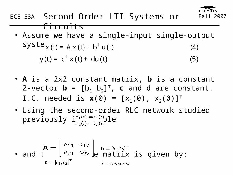
• Assume we have a single-input single-output system
• A is a 2x2 constant matrix, b is a constant 2-vector b = [b1 b2]T, c and d are constant. I.C. needed is x(0) = [x1(0), x2(0)]T
• Using the second-order RLC network studied previously in example
• and the 2x2 state matrix is given by:
ECE 53A Second Order LTI Systems or Circuits Fall 2007
_x(t) = Ax(t) +bT u(t) (4)
y(t) = cT x(t) +du(t) (5)
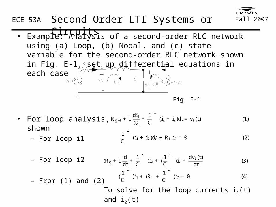
• Example: Analysis of a second-order RLC network using (a) Loop, (b) Nodal, and (c) state-variable for the second-order RLC network shown in Fig. E-1, set up differential equations in each case
• For loop analysis, we use KVL for the two loops shown– For loop i1
– For loop i2
– From (1) and (2)
ECE 53A Second Order LTI Systems or Circuits Fall 2007
Rgi1 +Ldi1d¿
+1C
Z(i1 +i2)dt = vs(t) (1)
1C
Z(i1 +i2)d¿ +RL i2 = 0 (2)
(Rg +Lddt
+1C
Z)i1 +(
1C
Z)i2 =
dvs(t)dt
(3)
(1C
Z)i1 +(RL +
1C
Z)i2 =0 (4)
To solve for the loop currents i1(t) and i2(t)
Fig. E-1
Vs(t)
Rs L
RL V2=VcV1
Vc
i1 iL i2
i1(t) i2(t)
+
-
+
-C

• We have studied the first-order RC-networks (and their dual RL networks), we now consider the second-order RLC-networks containing two energy storage elements, L and C. Consider the following RLC network
• The series RLC network in figure (4-1) has a single loop with loop current i(t) as shown in above figure and the KVL (loop or mesh) equation is given by
• Since• and
ECE 53A Second Order RLC Networks Fall 2007
RiR (t) +LdiL (t)dt
+vC (t) = vS (t) (1)
iR (t) = iL (t) = iC (t) = i(t) (2)
vC (t) =1C
ZiC (¿)d¿ (3)
Fig. (4-1)
Vs(t)
Rg L
Vc(t)
iR(t) iL(t)
i(t)
iC(t)
+
-

• Substituting these relationships to (1), we have
• Differentiate (13), we obtain
• Equation (5) is a second-order differential equation with constant coefficients. This is due to the fact that the circuit in Fig. 4-1 is a linear time-invariant (LTI) system with lumped circuit elements. The homogeneous part of the differential equation is
• And the characteristic equation is
• This characteristic equation is quadratic and has two roots.
ECE 53A Second Order RLC Networks Fall 2007
Ri +Ldidt
+1C
Zi(¿)d¿ = vS (t) (4)
Ld2idt2
+RLdidt
+1LC
i =ddtvS (t) (5)
Ld2idt2
+RLdidt
+1LC
i = C (6)
s2+RLs+
1LC
= 0 (7)
Second Order RLC Networks
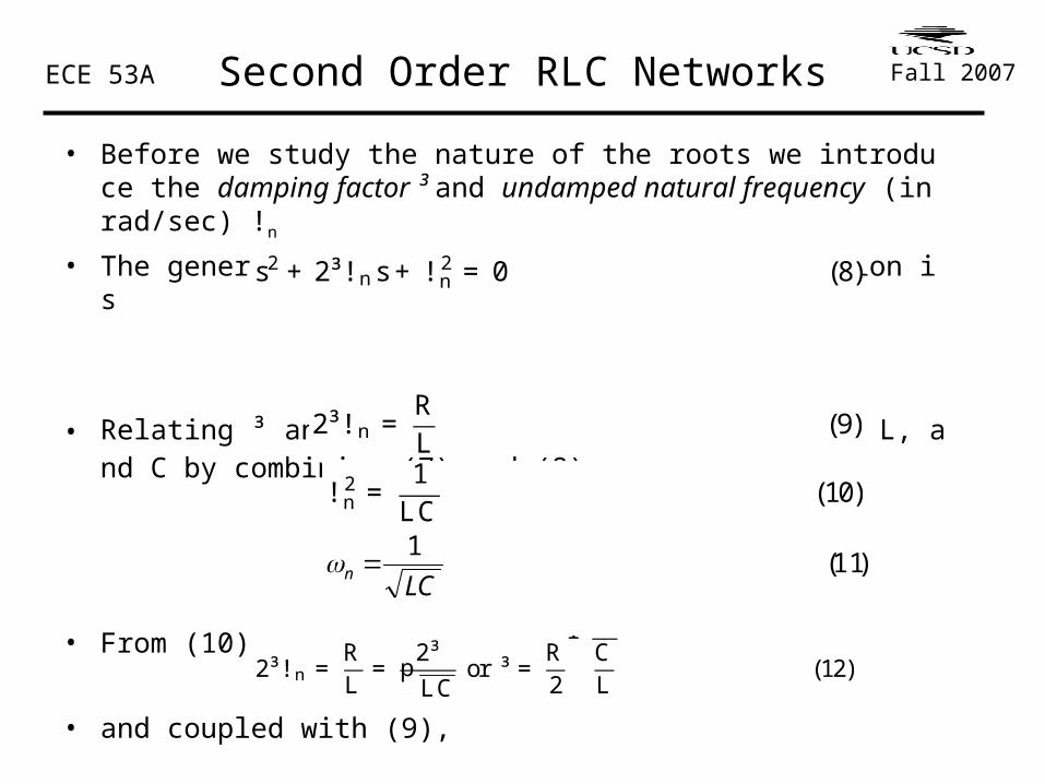
• Before we study the nature of the roots we introduce the damping factor ³ and undamped natural frequency (in rad/sec) !n
• The generic second-order characteristic equation is
• Relating ³ and !n with the circuit elements R, L, and C by combining (7) and (8),
• From (10),
• and coupled with (9),
ECE 53A Fall 2007
s2 +2³! ns+ ! 2n = 0 (8)
2³! n =RL
(9)
! 2n =
1LC
(10)
2³! n =RL
=2³
pLC
or ³ =R2
rCL
(12)
)11( 1
LCn

• Eq. (11) states that !n is determined by the LC product. In fact, for network analysis and system design, we can have two normalizations; one is for impedance and the other is for frequency. With impedance normalization, the circuit element value can be normalized, e.g., let R=1 With Frequency Normalization, we can normalize !n to 1rad/sec,. These normalizations simplify the analysis and design of circuits. This is especially convenient for the design and synthesis of circuits from specifications. With this in mind let !n = 1 rad/sec, the characteristic equation (8) reduces to
• The roots of this simplified quadratic equation are given by:
ECE 53A Second Order RLC Networks Fall 2007
s2 +2³s+1= 0; ! n =1rad=sec (13)
s1; s2 = ¡ ³ § 2p³2 ¡ 1 (14)

• The location of these zeros follow a locus, known as root locus, as shown in Fig. 4-2
ECE 53A Second Order RLC Networks Fall 2007
1
Fig. 4-2
¾
j!

• General nth-order LTI Circuits and System described by the state-variable formulation:
• For LTI systems, A, B, C and D are constant matrices
• State vector x = [x1, x2, …, xn]T
• Input vector u = [u1, u2, …, um]T
• Output vector y = [y1, y2, …, yp]T
• First-order LTI system, n=1
• Second-Order LTI System, n=2 (assume single input single output)
ECE 53AAppendix: State Variable Formulation for the General Linear Circuits and System Fall 2007
_x = Ax +Bu (1)
y = Cx +Du (2)
·_x1(t)_x2(t)
¸=
·a11 a12a21 a22
¸ ·x1(t)x2(t)
¸+·b1b2
¸u(t) (4)
y(t) = [c1 c2]·x1(t)x2(t)
¸+du(t) (5)
_x(t) =dx(t)dt
= ax(t) +bu(t) y(t) = cx(t) +du(t) (3)
• Laplace Transform of (3):
• Where
• From (6)
• Given the input u(t) and I.C. x(0), x(t) can be obtained by using the inverse Laplace Transform of (7). Let u(t)=δ(t), U(s)=1 and assume x(0)=0, we have
ECE 53ASolution of First Order State Equation in Transform Domain Fall 2007
sX (s) ¡ x(0) = aX (s) +bU(s) (6)
X (s)(s ¡ a) = bU(s) +x(0) or X (s) =bU(s) +x(0)
s ¡ a(7)
X (s) =b
s ¡ a(8)
Y (s) = cX (s) +d= c(b
s ¡ a) +d (9)
x(t) = (10)
y(t) = (11)

• For n=2, x=[x1, x2]T and
• Assume a single-input single-output LTI System, u and y are scalars and
• The Laplace Transform of (12) and (13) are given by
• or
ECE 53ASolution of Second Order State Equation in Transform Domain Fall 2007
·_x1(t)_x2(t)
¸=
·a11 a12a21 a22
¸ ·x1(t)x2(t)
¸+·b1b2
¸u(t) (12)
y(t) = [c1 c2]·x1(t)x2(t)
¸+du(t) (13)
sX (s) ¡ AX (s) = bU(S) +x(0) (14)
Y (s) = cTX (s) +dU(s) (15)
[sI n ¡ A ]X (s) = bU(s) +1sx(0) (16)
X (s) = [sI n ¡ A ]¡ 1·bU(s) +
1sx(0)
¸(17)
Where In = n x n identity matrix
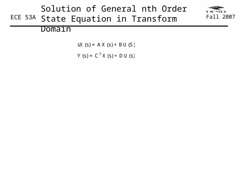
ECE 53ASolution of General nth Order State Equation in Transform Domain Fall 2007
sX (s) = AX (s) +BU(S)
Y (s) = C T X (s) +DU(s)

• (a) Given the resistive network shown in Figure P-1, find voltages and currents of all circuit elements (R’s, voltage and current sources), vk and ik k=1,2,…6. Use KCL and KVL equations based on trees and co-trees shown in Figure P-2.
• (b) Find the power entering (or leaving) of all circuit elements and show that the conservation of power is satisfied.
ECE 53A Homework Problem P - 1 Fall 2007
Vs1=1V Vs2=1VIs3=2A
Is4=1A
R1=1 R2=10
Figure P-1. A resistive network with 2 independent voltages sources and 2
independent current sources.
Figure P-2.Trees and co-trees for resistive network in Figure P-1.
Tree: solid lines, Cuts: dotted lines
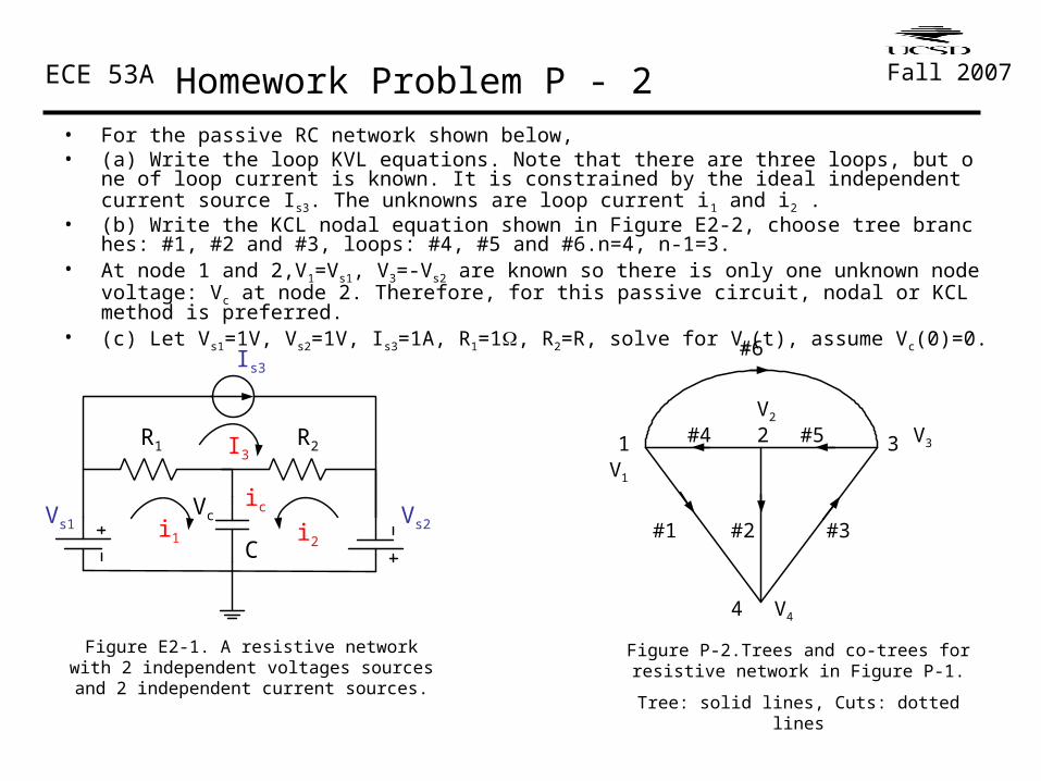
• For the passive RC network shown below,• (a) Write the loop KVL equations. Note that there are three loops, but one of loop current is known.
It is constrained by the ideal independent current source Is3. The unknowns are loop current i1 and i2 .
• (b) Write the KCL nodal equation shown in Figure E2-2, choose tree branches: #1, #2 and #3, loops: #4, #5 and #6.n=4, n-1=3.
• At node 1 and 2,V1=Vs1, V3=-Vs2 are known so there is only one unknown node voltage: Vc at node 2. Therefore, for this passive circuit, nodal or KCL method is preferred.
• (c) Let Vs1=1V, Vs2=1V, Is3=1A, R1=1, R2=R, solve for Vc(t), assume Vc(0)=0.
ECE 53A Homework Problem P - 2 Fall 2007
Vs1 Vs2
Is3
R1 R2
Figure E2-1. A resistive network with 2 independent voltages sources and 2
independent current sources.
Figure P-2.Trees and co-trees for resistive network in Figure P-1.
Tree: solid lines, Cuts: dotted lines
Vc
I3
i1 i2
ic
C#1 #2 #3
#4 #5
#6
1 2 3
4
V1
V2
V3
V4

• For the passive RC network shown in Figure E2-1,• (a) What is the order of this network?• (b) Write the loop (KVL) equations.• (c) Let Vs1=1V, Vs2=1V, is3=2A, Rs1=Rs2=0, R1=1, R2=R, from the results in part (b), solve
for the i1(t) and i2(t). What is the time constant for this network?• (d) Write the nodal (KCL) equations and solve for v1(t) and v2(t). Set the parameters
same as given in part (c), solve for v1(t), v2(t) and v(t).• (e) Write the state equation for this network, and solve for X(t) = vc(t). Since v(t)=vc(t),
your result should check that obtained in part (d).
ECE 53A Example 2 - 1 Fall 2007
Vs1 Vs2
Is3
R1 R2
Figure E2-1.Trees and co-trees for resistive network in Figure P-1.
Tree: solid lines, Cuts: dotted lines
Is3
i1 i2
V1 V2
VRs1 Rs2

• Last problem of FINAL (20%)• (15%)(a) In this RC network, let R1=R2=1, and R3=R, find Vc(t). Note that si
nce there is one energy storage element C in this circuit, it is a first-order RC network and you should get a first-order differential equation.
• (5%)(b) Assuming that the initial condition is given by vc(0)=0, and the two constant voltage sources vs1 and vs2 are applied at t=0, find vc(t), t¸0.
ECE 53A Example 2 - 1 Fall 2007
Vs1=1V
R1 R2
Figure E2-1.Trees and co-trees for resistive network in Figure P-1.
Tree: solid lines, Cuts: dotted lines
Vc
V2
Vc(t)
R3
Vs2=1V
ic+
-

ECE 53A Example 2 - 1 Fall 2007
1 3 2
4
R1, R2, R3 are links.
KCL at node 3 (vc) first order differential equation.
(1R1
+1R2
+Cddt)Vc(t) ¡
1R1
Vs1 ¡1R2
Vs2 =0
(1R1
+1R2
+Cddt)Vc(t)¡
1R1
Vs1¡1R2
Vs2=0
(G1+G2+sC)Vc(s) =G1
s+G2
s
Assume Vc(0)=0
Vs1 and Vs2 are constants.

• Delays in Logic Circuits• Transition time in CMOS• Delays in connected CMOS inverters and CMOS logic gates• Even simple models of gate switching will provide reasonable
estimate of system limitations
ECE 53A Gate Delay and RC Circuits Fall 2007
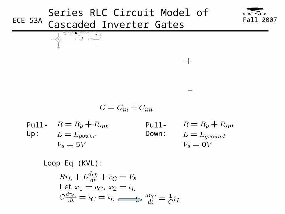
ECE 53ASeries RLC Circuit Model of Cascaded Inverter Gates
Fall 2007
Loop Eq (KVL):
Pull-Up: Pull-Down:
Vs(t)
R L
Vc(t)
iL(t)
i(t)
iC(t)
C
t=0
+
-
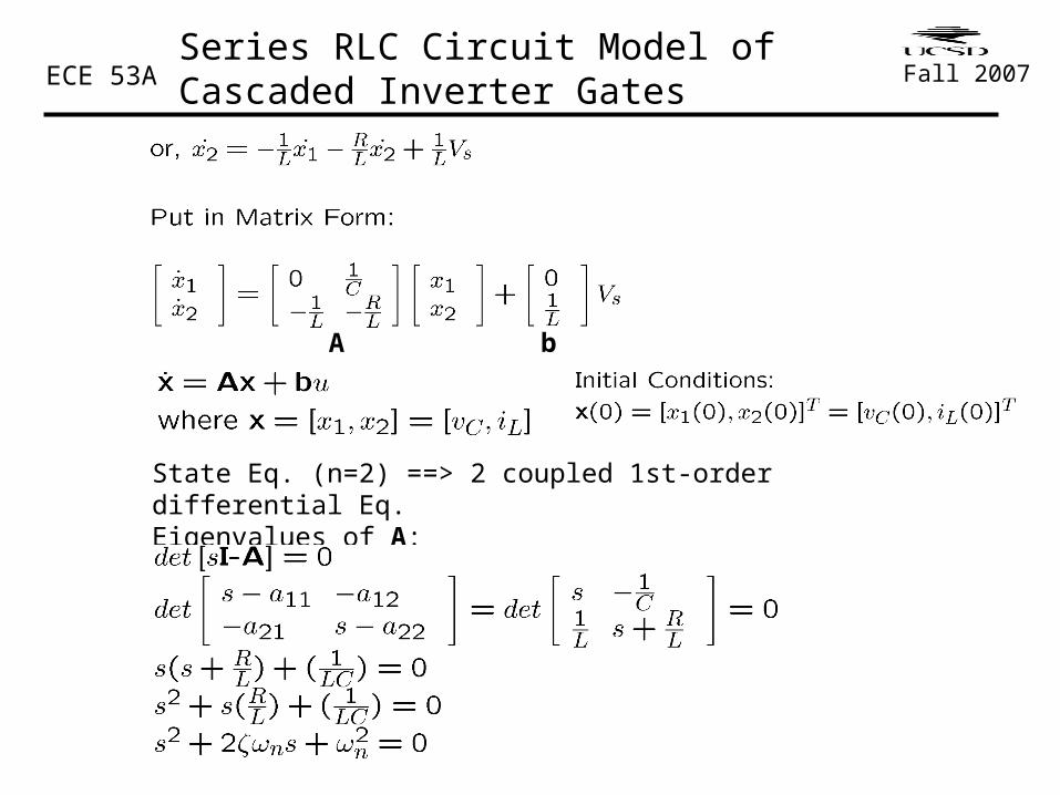
ECE 53ASeries RLC Circuit Model of Cascaded Inverter Gates
Fall 2007
State Eq. (n=2) ==> 2 coupled 1st-order differential Eq.Eigenvalues of A:
A b

ECE 53AEquivalent Circuit For the Cascaded Inverter Pair, Using a Two Lumped Interconnect Model
Fall 2007
(1R1
+1R2
+Cddt)Vc(t) ¡
1R1
Vs1 ¡1R2
Vs2 =0
Natural Frequencies δ1, δ2 >0
Homogeneous Eq.:
¾
j!
-¾1-¾2
State Variables:
x1=vc1
x2=vc2
Vs(t)
R1
C2
R2t=0
C1
+
-
Vc1
+
-
Vc2
+
-
Vo+
-
s-plane
s = ¾+j!

• Voltage vC(t) at the Input of the load inverter in Example 6.2:
ECE 53A Fall 2007
• Note that the coupled inverters undergo a pull-down transition at t=0 and are subsequently pulled up at t=0.3ns. Note also that the voltage vc(t) in the RLC model continues to fall for a period after the second switching event; this is due to the presence of the inductor, which attempts to force the current to flow in the same direction.