ece594a notes set 1, device models and device characteristics
TRANSCRIPT

ECE145A /218CA notes, M. Rodwell, copyrighted
ECE145a / 218a: Notes Set 5 device models & device characteristics:
Mark Rodwell
University of California, Santa Barbara
[email protected] 805-893-3244, 805-893-3262 fax

ECE145A /218CA notes, M. Rodwell, copyrighted
Content:
s.frequencie Cutoff
models (JFET) HEMT
Models MOSFET
Models TransistorBipolar

ECE145A /218CA notes, M. Rodwell, copyrighted
Active Devices:
Bipolar Transistors

ECE145A /218CA notes, M. Rodwell, copyrighted
HBT Physical Structure

ECE145A /218CA notes, M. Rodwell, copyrighted
Increasing total emitter area
current. specified someat bandwidth peak reach toselectedgenerally areaEmitter
current. maximum theincreases fingers) multipleor , g(increasin areaemitter theIncreasing EL
area)emitter total/(EE IJ

ECE145A /218CA notes, M. Rodwell, copyrighted
0
5
10
15
20
0 1 2 3 4V
ce
mA
/m
2
Bipolar Transistor: DC characteristics: common-emitter
Vce,sat
Vbr,ceo
bc II
10-12
10-10
10-8
10-6
10-4
10-2
0 0.25 0.5 0.75 1
I c ,
I b (
A)
Vbe
(V)
Ic
Ib
densitiescurrent higher at fail and
e,approximat are ipsrelationsh These
/ and
:elyApproximat
/ cb
nkTqV
sc IIeII be

ECE145A /218CA notes, M. Rodwell, copyrighted
HBT hybrid-Pi equivalent-circuit model
cbf Ccbi
Ccbx
Rbe
RbbB C
E
Rex
Rc
Vbe
CjeCbe,diff =gm f
gmVbee-jc
mbe gR /
0.8)~ (typically 10 cj
mom egg
collectorbasef
)/( qnkT
I
V
Ig C
BE
Cmo
circuits. somein t significan becan neglected,often though , termThe cje
resitances parasitic :,,
collector and basein sansit timecarrier tr :,
ecapacitancdiffusion :
escapacitancdepletion :,,
cb
,
ceb
diffbe
cbxcbije
RRR
C
CCC

ECE145A /218CA notes, M. Rodwell, copyrighted
Bipolar Transistor T-model
)(1
1
1
1
1
1
exp1
1)(
0
0
0
cb
cb
c
b
j
jj
jj
The approximations above, if taken to first order in , produce the hybrid pi model.
The T model is more convenient for common-base amplifier analysis.

ECE145A /218CA notes, M. Rodwell, copyrighted
How model varies as emitter area is increased
Ccbi
Ccbx
Rbe
RbbB C
E
Rex
Rc
Vbe
CjeCbe,diff =gm f
gmVbee-jc
pages. previous on the formulas by thegiven are and ,
N.:1 decrease sresistance all 1,:N increase escapacitanc All
parallel.in HBTs N wiringas same 1:Nby areaemitter theIncreasing
mbebe gRC

ECE145A /218CA notes, M. Rodwell, copyrighted
Active Devices:
Silicon MOSFETs

ECE145A /218CA notes, M. Rodwell, copyrighted
Planar Bulk MOSFET
N+ source N+ drain
source contact (silicide) drain contact (silicide)
N+ polygate
gate metal(silicide) dielectric
sidewall
gate oxide
P substrate
S D S D S D S
G
G
Wg
Cross-Section Layout (multi-finger)
P substrate
gatedielectric
N+polysilicongate
inversionlayer

ECE145A /218CA notes, M. Rodwell, copyrighted
MOSFET DC Characteristics
ID
VDS
increasingVGS
gthgsgoxD LVVWcI 2/)(
current limitedmobility
2
,
)(
current limitedvelocity
, thgssatgoxvD VVvWcI
1
Expression dGeneralize
,
2
,
D
D
vD
D
I
I
I
I
Id
VgsVth
mobility-limited
velocity-limited
: voltageknee thenlarger tha voltagesdrainFor

ECE145A /218CA notes, M. Rodwell, copyrighted
Knee Voltage: Mobility-Limited Case
VGD
=Vth
regionscurrent -constant and Ohmic the
betweenboundary thedefines voltageknee TheID
VDS
increasingVGS
Oh
mic
constant-current
thgsdsdg VVVV
whenoccurs curve in knee the
regime, limited-mobility theIn
IDR
D
VGD
=Vth
IDR
S
s.resistance drain & source parasitic theacross drops
by voltage increasedfurther is Voltage KneeThe

ECE145A /218CA notes, M. Rodwell, copyrighted
Knee Voltage: Velocity-Limited Case
/ whenoccurs
curve in knee theregime, limited- velocity theIn
gsatds LvV
s.resistance drain & source
parasitic theacross drops by voltage
increasedfurther is Voltage Knee theAgain,
VDS
=vsat
Lg/
IDR
D
VDS
=vsat
Lg/
IDR
S

ECE145A /218CA notes, M. Rodwell, copyrighted
DC Characteristics---Far Above Threshold
/ where
1/)(for )(
gsat
thgsthgssatgoxD
LvV
VVVVVVvWcI
Id
VgsVth
V

ECE145A /218CA notes, M. Rodwell, copyrighted
MOSFET Transconductance
gthgsgox
GS
Dm
gthgsgoxD
LVVWcV
Ig
LVVWcI
/)(
2/)(
limitedmobility
2
,
satgox
GS
Dm
thgssatgoxvD
vWcV
Ig
VVvWcI
)(
limitedvelocity
,
Id
VgsVth
V
gm
VgsVth
V
mobility-limited
velocity-limited

ECE145A /218CA notes, M. Rodwell, copyrighted
Linear vs. Square-Law Characteristics: 90 nm

ECE145A /218CA notes, M. Rodwell, copyrighted
90 nm MOSFET DC Characteristics
3V~1/ V 6.0||
mm/S 7.0μm/mS 7.0/
channel-P
3V~1/ V 6.0
mm/S 4.1μm/mS 4.1/
channel-N
th
satoxgm
th
satoxgm
V
vcWg
V
vcWg

ECE145A /218CA notes, M. Rodwell, copyrighted
Device Structure and Model: multi-finger device
mi
gds
gogg
eq
gs
o
gogd
thgsg
eq
geff
eq
m
gR
NWG
WkNWLT
C
k
WkC
VVNWT
NWvT
g
/1~
mfF/)5.03.0(
or
gdb
gsb
gs
gd
endg
g
sg
NWC
NWC
NWR
NWR
N
R
N
W
LR
/1
/1
212~
CgdRg
Ri
Cgs Vg’s’
gmVg’s’ Gds
Rs
RdG
D
S
Csb
Cdb
CgdRg
Ri
Cgs Vg’s’
gmVg’s’ Gds
Rs
G
D
S
Csb
Cdb
S D S D S D S
G
G
Wg
contacts substrate ample -
fingers gateshort -
using Increase maxf

ECE145A /218CA notes, M. Rodwell, copyrighted
Cgd
Rin
Cgsx Vg’s’
gmxVg’s’ GdsxG
D
S
Cdb
Csb
Oversimplified Model
igsin
sm
dsdsx
sm
gs
gsx
sm
mmx
RRRR
Rg
GG
Rg
CC
Rg
gg
~
1
~
1~
1~
etc analysis, hand roughFor CgdRg
Ri
Cgs Vg’s’
gmVg’s’ Gds
Rs
G
D
S
Csb
Cdb
gdgdsigs
gddsmgdmgs
CRGRRR
ff
CRRgCgCf
2)(2~
)(//~2/1
sfrequencie cutoff eApproximat
max

ECE145A /218CA notes, M. Rodwell, copyrighted
Active Devices:
III-V
Field-Effect Transistors

ECE145A /218CA notes, M. Rodwell, copyrighted
FET with Heterojunction for Gate Barrier→ HEMT
gate. and channel betweenbarrier for
tionheterojunctor semiconduc withFET
:HEMT
Source Drain
Gate
drawing: K. Shinohara, HRL
N+ InGaAs contact layer
InAlAs gate barrier layer
undoped InGaAs channel
Brar. B.:drawing

ECE145A /218CA notes, M. Rodwell, copyrighted
HEMTs: Typical interdigitated structure
gate
drain
source
Note multiple gate fingers.

ECE145A /218CA notes, M. Rodwell, copyrighted
HEMT: approximate equivalent circuit model
Idss. Cgs, Cgd, gm, Gds all scale proportionally with gate periphery
Ri, Rs scale proportionally with (1/ gate periphery)
Rg scales proportionally to (gate finger length)/(number fingers)

ECE145A /218CA notes, M. Rodwell, copyrighted
HEMT DC-IV characteristics
V 0.6 c.a. thanpositive more for current draw willgate
channel; and gate between diodeSchottky
gsV
Scientific Teledyne Shinohara, K. :Data

ECE145A /218CA notes, M. Rodwell, copyrighted
Figures of Merit

ECE145A /218CA notes, M. Rodwell, copyrighted
Transistor figures of Merit
Transistor small-signal bandwidth is typically stated in terms of
the figures of merit f and fmax
In order to understand these figures of merit, we must introduce
device power gain.
These power gains will be studied in more detail
later in the course.

ECE145A /218CA notes, M. Rodwell, copyrighted
Definition of short-circuit current gain
Ri
Cgs Vg's
gmVg's Rds
S
G
D
D
S
G example: FET
small-signal model
Ri
Cgs Vg's
gmVg's RdsIin
Iout
short-circuit current gain:
drive input with AC current,
short output, measure
Iout/Iin
jf
f
Cj
g
I
Vg
I
ICjIV
gs
m
in
gsm
in
outgsings /

ECE145A /218CA notes, M. Rodwell, copyrighted
Variation of H21 with frequency: Bipolar Transistors
0
10
20
30
40
50
1 10 102
Ga
ins (
dB
)
Frequency (GHz)
h21
U
VCE
= 1 V, JC = 1.5 mA/um
2
fMAX
= 295 GHz
f = 295 GHz
fF9.6cbxC
fF2.3cbiC 48bbR
7.4exR
ebmVg 'ebV '
E
B C
diffC
fF172
jeC
fF34
R433
7000cbr
500cer
)exp( cmom jgg
fmodiff gC
R mg
H21 is plotted in dB.
because H21 is a
current gain:
)(log*20)( 211021 HHdB
jfffH
gm
//1
1)(
:/R ofeffect of Because
21

ECE145A /218CA notes, M. Rodwell, copyrighted
Current-gain cutoff frequency: Bipolar Transistors
collex
E
bc
E
jecollectorbase RRqI
kTC
qI
kTC
f
2
1
nbbase DT 22 satccollector vT 2
base
BC grade
collector
N+ sub collector
semi-insulating InP substrate
emitter
emittercontact
base contact
cT
b,contW
eW
ebW
underW
N- drift collector
base contact
collector contact
bT
cW
EB grade
Ccbi
Ccbx
Rbe
RbbB C
E
Rex
Rc
Vbe
CjeCbe,diff =gm f
gmVbee-jc

ECE145A /218CA notes, M. Rodwell, copyrighted
Current-gain cutoff frequency: Field-Effect Transistors
N+ source N+ drain
source contact (silicide) drain contact (silicide)
N+ polygate
gate metal(silicide) dielectric
sidewall
gate oxide
P substrate
)(2 gdgs
m
CC
gf
CgdRg
Ri
Cgs Vg’s’
gmVg’s’ Gds
Rs
G
D
S
Csb
Cdb

ECE145A /218CA notes, M. Rodwell, copyrighted
Maximum Power Transfer Theorem
gen
RMSgen
avg
genloadgenload
R
VP
RRXX
4
ispower generator available thecalled delivered,power The
***matching impedance conjugate*** called is this
and
if load togenerator from ed transferrispower Maximum
2
)(,
generator load
Vgen
RgenXgenXload Rload

ECE145A /218CA notes, M. Rodwell, copyrighted
Impedance Matching
Maximum power transfer can be obtained by adding a
***lossless*** (no resistances) impedance matching network
between the generator and the load:
generator load
Vgen
RgenXgenXload Rload
match
loadZ*
loadZgenZ *
genZ

ECE145A /218CA notes, M. Rodwell, copyrighted
Maximum Available Power Gain (if it exists)
Ri
Cgs Vg's
gmVg's Rds
generator
losslessmatchingnetwork
Rgen
Vgen
losslessmatchingnetwork
RL
load
The transistor or amplifier is connected to generator and load via lossless
matching networks. If it is possible to match at both input and output, then the
power gain is called the *maximum available gain* (MAG)
Detailed microwave circuit theory (see later notes) indicates that this
procedure often produces an oscillator (if the device is “potentially unstable”) .
In that case we must define Maximum stable gain

ECE145A /218CA notes, M. Rodwell, copyrighted
Maximum Stable Power Gain (if MAG does not exist)
If the device is potentially unstable (usually due to strong feedback through
Cgd as indicated), addition of a minimum amount of series/shunt resistance to
the device input/output will prevent oscillation, and the device can then be
matched. The resulting power gain is called the
Maximum stable power gain.
Ri
Cgs Vg's
gmVg's
Rds
generator
losslessmatchingnetwork
Rgen
Vgen
losslessmatchingnetwork
RL
load
resistiveloss
(stabiliz-ation)

ECE145A /218CA notes, M. Rodwell, copyrighted
Unilateral power gain
Ri
Cgs Vg's
gmVg's Rds
generator
losslessmatchingnetwork
Rgen
Vgen
losslessmatchingnetwork
RL
load
seriesfeedback
shuntfeedback
If the device is potentially unstable (due to strong feedback ), addition of
lossless reactive feedback as indicated can cancel the feedback and prevent
oscillation. The device can then be matched. The resulting power gain is called
Mason’s invariant power gain **or** the Unilateral power gain , U.

ECE145A /218CA notes, M. Rodwell, copyrighted
Power-Gain Cutoff Frequency (Fmax)
This is the frequency at which the device Unilateral power gain reaches
unity.
The maximum available gain (either in the forward or reverse direction)
also reaches unity at the same frequency
cbibbcbibbcebb
ce
dggdsgsi
CR
f
CRfRR
ff
R
CRfGRRR
ff
82/2
:large) being ( sTransistorr For Bipola
2)(2
:sTransistor Effect-For Field
max
max
CgdRg
Ri
Cgs Vg’s’
gmVg’s’ Gds
Rs
G
D
S
Csb
Cdb
Ccbi
Ccbx
Rbe
RbbB C
E
Rex
Rc
Vbe
CjeCbe,diff =gm f
gmVbee-jc

ECE145A /218CA notes, M. Rodwell, copyrighted
Power gains of a typical transistor
0
5
10
15
20
25
30
35
40
1 10 100
Ga
ins, d
B
Frequency, GHz
MAG/MSG
common base
U: all 3
MAG/MSG
common collector
MAG/MSG
common emitter
The inflection in the curves is the break between unstable (MSG) at lower frequencies
and stable (MAG) at higher frequencies.
MAG/MSG is directly relevant for RF/microwave/mm-wave IC design.
Because U has -20 dB/decade slope, it is used to extrapolate measurements to determine fmax
fmax

ECE145A /218CA notes, M. Rodwell, copyrighted
End

ECE145A /218CA notes, M. Rodwell, copyrighted
Appendix
(optional)

ECE145A /218CA notes, M. Rodwell, copyrighted
Bipolar Transistor
Operation

ECE145A /218CA notes, M. Rodwell, copyrighted
Bipolar Transistor ~ MOSFET Below Threshold
ceV
voltagecollector with little varies
it through pass base reaching electrons allAlmost
)/exp(
al)(exponenti thermalison distributienergy emitter Because
c
bec
I
kTqVI

ECE145A /218CA notes, M. Rodwell, copyrighted
Bipolar Transistor ~ MOSFET Below Threshold
cI
beV ceV
voltagecollector with little varies
it through pass base reaching electrons allAlmost
)/exp(
al)(exponenti thermalison distributienergy emitter Because
c
bec
I
kTqVI

ECE145A /218CA notes, M. Rodwell, copyrighted
HBT Equivalent
Circuit Model

ECE145A /218CA notes, M. Rodwell, copyrighted
Physical structure, symbolic
base
BC grade
collector
N+ sub collector
semi-insulating InP substrate
emitter
emittercontact
base contact
cT
b,contW
eW
ebW
underW
N- drift collector
base contact
collector contact
bT
cW
EB grade
drawing lar toperpendicu
LengthStripe Device EL

ECE145A /218CA notes, M. Rodwell, copyrighted
Bipolar Transistor DC-IV Characteristics

ECE145A /218CA notes, M. Rodwell, copyrighted
Bipolar Transistor: Carrier Transit Times

ECE145A /218CA notes, M. Rodwell, copyrighted
Base resistance & collector-base capacitance
2008 Feb.IEEE Proc.2001, Nov. EDLIEEE Rodwell(see class of scope beyond Details
and into of splitting ddistribute are and
12
1
6
1
2
emitterunder spreading contact under spreading rmcontact te
torsemiconduc
__
,
,
cbicbxcbcb bb
c
eccb
sheetbase
E
Esheetbase
E
contactb
contbE
contactbb
bb
CCCCR
T
LWC
L
W
L
W
WLR
R
drawing lar toperpendicu
LengthStripe Device EL

ECE145A /218CA notes, M. Rodwell, copyrighted
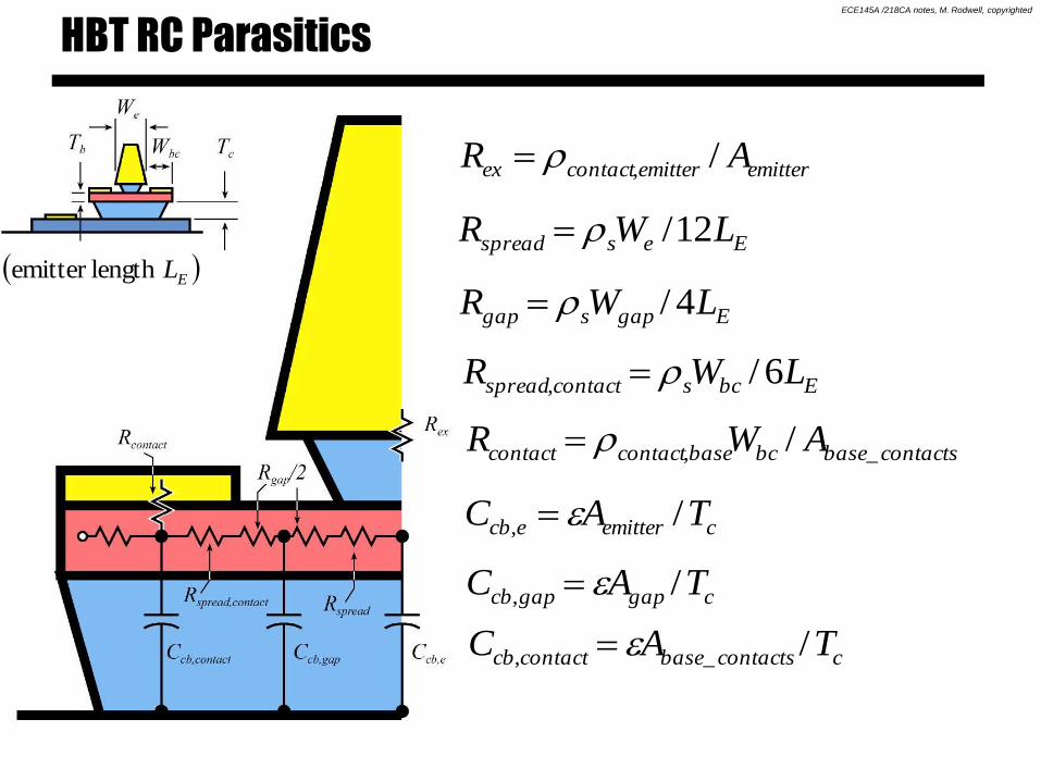
HBT RC Parasitics
base contact width
< 2 transfer lengths
→ simple analysis
Limiting case of
Pulfrey / Vaidyanathan
fmax model.
ECE145A /218CA notes, M. Rodwell, copyrighted
HBT RC Parasitics
emitteremittercontactex AR /,
Eesspread LWR 12/ ELlength emitter
Egapsgap LWR 4/
Ebcscontactspread LWR 6/,
contactsbasebcbasecontactcontact AWR _, /
cemitterecb TAC /,
cgapgapcb TAC /,
ccontactsbasecontactcb TAC /_,

ECE145A /218CA notes, M. Rodwell, copyrighted
Base-Collector Time Constant & Fmax.
where8
max
cbibbCR
ff
)(
)2/(
,,
,,
,
spreadgapcontactspreadcontactecb
gapcontactspreadcontactgapcb
contactcontactcbcbibbcb
RRRRC
RRRC
RCCR

ECE145A /218CA notes, M. Rodwell, copyrighted
Relationship to HBT Equivalent Circuit Model
contactspreadcontactgapspreadbb RRRRR ,
contactcbgapcbecbcbicbx CCCCC ,,,
)(
)2/(
,,
,,,
spreadgapcontactspreadcontactecb
gapcontactspreadcontactgapcbcontactcontactcbcbibb
RRRRC
RRRCRCCR

ECE145A /218CA notes, M. Rodwell, copyrighted
Field-Effect Transistor
Operation (Approximate)

ECE145A /218CA notes, M. Rodwell, copyrighted
Field-Effect Transistor Operation
source drain
gate
Positive Gate Voltage
→ reduced energy barrier
→ increased drain current

ECE145A /218CA notes, M. Rodwell, copyrighted
Field-Effect Transistor Operation
source drain
gate
Positive Gate Voltage
→ reduced energy barrier
→ increased drain current

ECE145A /218CA notes, M. Rodwell, copyrighted
FETs: Basic Operation
chdC
/ where/ electrongd vLQI
/~ DACgs
/ and / where chdgdgsmdsdsgsmd CGCgVGVgI
dschdgsgs VCVCQ

ECE145A /218CA notes, M. Rodwell, copyrighted
FET Characteristics
chdC /~ DACgs
dsdsgsmd VGVgI
ID
VDS
increasingVGS
electrongchdgdgsm vLCGCg / / /

ECE145A /218CA notes, M. Rodwell, copyrighted
FET Parasitic Capacitances (Estimate)
oxgm TvWg /~/
oxgggs TLWC /~/
~/, gfgs WC
subcgsb TLWC /~/
~/ ggd WC