ecma tr/93
TRANSCRIPT

ECMA TR/93 1st Edition / December 2007
Measuring Emissions from Modules

COPYRIGHT PROTECTED DOCUMENT
© Ecma International 2007

Ecma International Rue du Rhône 114 CH-1204 Geneva T/F: +41 22 849 6000/01 www.ecma-international.org
IW TR-093.doc 02/01/2008 14:39:00
Measuring Emissions from Modules
Technical Report ECMA TR/93 1st Edition / December 2007

.

Introduction
Manufacturers need to know how the insertion of add-on modules affects the compliance of their products with applicable EMC requirements. VCCI, an Ecma member, developed a method to determine the RF disturbances generated by a module into its power feeding leads. This Ecma Technical Report develops that measurement method. Conducted RF disturbances determined according to that method can be used as a measure of the contribution of an add-on module to the RF disturbances generated by the host appliance. The method may be used to compare various modules or to estimate the interference potential of a specific module, but is not intended to be used to assess compliance with applicable national or international standards.
This Ecma Technical Report has been adopted by the General Assembly of December 2007.

- i -
Table of contents
1 Scope 1
2 References 1
3 Definit ions and abreviations 1
3.1 Defin i t ions 1 3.1.1 Magnet ic probe 1 3.1.2 Module 1
3.2 Abbreviat ions 1
4 Measuring faci l i ty 1
4.1 Shielded room 1
4.2 Fixture for magnet ic probe 1
4.3 Measur ing instruments 2 4.3.1 Measur ing receiver 2 4.3.2 Spectrum analyzer 2 4.3.3 Magnet ic probe 2
4.4 Test board 4
5 Measuring Method 4
5.1 Temperature 4
5.2 Power supply 4
5.3 Posi t ioning of MUT and magnet ic probe 4 5.3.1 Posi t ioning of MUT 4 5.3.2 Space and posi t ioning of magnet ic probe 4
5.4 Measurement procedure 5
5.5 Report ing measurement resul ts 6
6 Method for cal ibrating the magnetic probe 7
6.1 Appl icat ion 7
6.2 Measur ing instruments used for cal ibrat ing the magnet ic probe 7 6.2.1 Preampl i f ier 7 6.2.2 Micro-str ip l ine 7 6.2.3 Other measur ing instruments 7
6.3 Cal ibrat ion procedures 7
Annex A Condit ions for measuring emissions from the Module Under Test 9
A.1 Test board 9
- ii -
A.1.1 Layer p lacement 9
A.1.2 Decoupl ing capaci tor 10
A.1.3 Other components 10
A.1.4 Measuring c ircui t 10
A.2 Integrated memory 11
A.2.1 Placement of MUT 11
A.2.2 Operat ing condi t ions 11
A.3 Integrated disk unit 12
A.3.1 Placement of MUT 12
A.3.2 Operat ing condi t ions 12
A.4 Interface board 14
A.4.1 Placement of MUT 14
A.4.2 Operat ing condi t ions 14
Annex B Current measurements w ith a magnetic probe 17
Annex C Inf luence of magnetic-probe placement on measured values 19
- 1 -
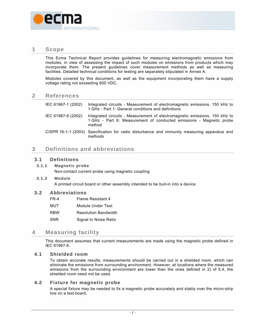
1 Scope This Ecma Technical Report provides guidelines for measuring electromagnetic emissions from modules, in view of assessing the impact of such modules on emissions from products which may incorporate them. The present guidelines cover measurement methods as well as measuring facilities. Detailed technical conditions for testing are separately stipulated in Annex A.
Modules covered by this document, as well as the equipment incorporating them have a supply voltage rating not exceeding 600 VDC.
2 References IEC 61967-1 (2002) Integrated circuits - Measurement of electromagnetic emissions, 150 kHz to
1 GHz - Part 1: General conditions and definitions
IEC 61967-6 (2002) Integrated circuits - Measurement of electromagnetic emissions, 150 kHz to 1 GHz - Part 6: Measurement of conducted emissions - Magnetic probe method
CISPR 16-1-1 (2003) Specification for radio disturbance and immunity measuring apparatus and methods
3 Definitions and abbreviations
3.1 Definitions 3.1.1 Magnetic probe
Non-contact current probe using magnetic coupling
3.1.2 Module A printed circuit board or other assembly intended to be buit-in into a device
3.2 Abbreviations FR-4 Flame Resistant 4
MUT Module Under Test
RBW Resolution Bandwidth
SNR Signal to Noise Ratio
4 Measuring facility This document assumes that current measurements are made using the magnetic probe defined in IEC 61967-6.
4.1 Shielded room To obtain accurate results, measurements should be carried out in a shielded room, which can eliminate the emissions from surrounding environment. However, at locations where the measured emissions from the surrounding environment are lower than the ones defined in 2) of 5.4, the shielded room need not be used.
4.2 Fixture for magnetic probe A special fixture may be needed to fix a magnetic probe accurately and stably over the micro-strip line on a test board.

- 2 -
4.3 Measuring instruments To obtain accurate and repeatable results, measuring instruments should meet the conditions stated in CISPR 16-1-1 (2003). These instruments - for example, measuring receivers, spectrum analyzers, and cables – are be periodically calibrated and checked, ideally once a year. The method used for calibration is either directly or indirectly traceable to national standards. The procedure for calibrating the magnetic probe is described in Clause 6.
4.3.1 Measuring receiver
Table 1 – Sett ings of frequency range and bandwidth of the measuring receiver
Frequency range 10 MHz – 30 MHz 30 MHz – 1 GHz
6 dB bandwidth 9 kHz 120 kHz
For details about the settings of the measuring receiver, refer to CISPR 16-1-1 (2003).
4.3.2 Spectrum analyzer
Table 2 – Sett ings of frequency range and RBW of the spectrum analyzer
Frequency range 10 MHz – 30 MHz 30 MHz – 1 GHz
3 dB RBW 10 kHz 100 kHz
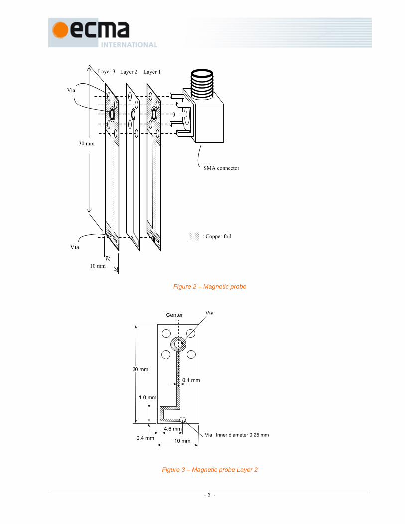
4.3.3 Magnetic probe The magnetic probe is constructed with a shield against static electricity. The structure of the magnetic probe is shown in Figures 1 through 4.
Figure 1 – Magnetic probe Layer 1 and 3
1.8 mm
30 mm 0.8 mm
Via : Inner diameter 0.25 mm
0.2 mm
10 mm 8.4 mm
0.1 mm
10 mm
Center Via
Via
- 3 -
Figure 2 – Magnetic probe
Figure 3 – Magnetic probe Layer 2
: Copper foil
SMA connector
Layer 1 Layer 2 Layer 3
30 mm
Via
Via
10 mm
30 mm
Via
0.1 mm
10 mm
4.6 mm
1.0 mm
Center
ViaInner diameter 0.25 mm 0.4 mm

- 4 -
Figure 4 – Magnetic probe structure of each layer
4.4 Test board To measure emissions from a module a test board has to be used to which the MUT is attached.
A micro-strip line to measure with the magnetic probe shall be provided on the test board. For the details, consult Annex A.
5 Measuring Method
5.1 Temperature The ambient temperature of the actual test facility is within the range of 15 °C to 35 °C. The temperature during measurement is being recorded.
5.2 Power supply The power supply feeds the MUT with the required voltage and current for that MUT.
5.3 Positioning of MUT and magnetic probe 5.3.1 Posit ioning of MUT
The MUT is positioned on the top layer of the test board, as detailed in Annex A.
5.3.2 Spacing and posit ioning of magnetic probe The magnetic probe is positioned in such a manner that:
- the space between the tip of the magnetic probe and the micro-strip line is 1.0 mm ± 0.1 mm;
Layer 3
Layer 2
Layer 1 Insulator
Structure of each layer layer 1 :
Thickness of copper foil 0.035 mm Thickness of Insulator 0.2 mm layer 2 : Thickness of copper foil 0.035 mm
Thickness of Insulator 0.2 mm layer 3:
Thickness of copper foil 0.035 mm
Insulator
Center
Insulator ( glass epoxy )

- 5 -
- the positioning angle of the magnetic probe to the micro-strip line is less than 5 degrees;
- the magnetic probe is at the center of the longer dimension of the micro-strip line.
More details can be found in Annex C.
5.4 Measurement procedure Measurements shall be taken in the following steps:
1) Setup
Figures 5 and 6 show the test setup and its general configuration. More details can be found in Annex A.
Figure 5 – Test setup
Micro-strip line Space between micro-strip line and magnetic probe tip 1.0 ± 0.1 mm
Magnetic probe
Ground layer for micro-strip line
(layer 2)
C2
MUT
Layer 1
Bottom layer
Test board

- 6 -
Figure 6 – Configuration of measuring facility
2) Measurement of ambient noise
Ambient noise is measured with the MUT not connected to the test board, but with all other parts of the test setup powered on. The measured levels should be 6 dB or more lower than the limits set for the MUT.
3) Measurement of MUT emission
The MUT is connected to the test board and the emission is measured while the MUT is in operation. The recorded values should be the highest of the results of at least 10 consecutive measurements, made while the MUT is continuously operated. An attempt should be made to maximize the emission, in a way which is consistent with the typical applications of the MUT. More details can be found in Annex A.
4) Transformation of measured data to current
When the measuring instrument does not provide a direct reading of the current in the micro-strip line under the probe, that current can be calculated using formula:
I = Vp + Cf – Ch dB(A)
Where:
I is RF current, in dB(A).
Vp is the output voltage of the magnetic probe, in dB(V).
Cf is the calibration factor of the magnetic probe, in dB(A/m/V).
Ch is the coupling factor of the test board, in dB(1/m).
More details about current measurements with a magnetic probe can be found in Annex A.1.
5.5 Reporting measurement results The test report should indicate at least the six highest emission values recorded according to 5.4 point 3), together with the frequencies at which they have been recorded. The test report should also document the test configuration to allow accurate repetition of the test.
Spectrum analyzer
MUT
Magnetic probe
Preamplifier
Cable
Test board for MUT

- 7 -
6 Method for calibrating the magnetic probe
6.1 Application Annex B describes the procedure to calibrate the magnetic probe by using a micro-strip line as an electromagnetic-wave generator.
The following IEC documents are used as reference for the calibration of the magnetic probe:
- IEC 61967-1 (2002
- IEC 61967-6 (2002).
Other instruments should be calibrated based on CISPR 16-1-1 (2003) describing the calibration method for a shielded-loop type magnetic probe.
6.2 Measuring instruments used for calibrating the magnetic probe 6.2.1 Preamplif ier
A preamplifier may be used to obtain a sufficient SNR.
6.2.2 Micro-str ip l ine A micro-strip line structure such as that shown in Figure 7 should be used as reference signal source. The insulator thickness (h) of the board that composes the micro-strip line should be 0.6 mm, and the characteristic impedance should be 50 ± 5 Ω.
When FR-4 is used for the board (dielectric constant εr = 4.7), the strip conductor width (W) should be 1.0 mm, and the ground plane width (Wg) of the micro-strip line should be at least 50 mm. The micro-strip line as structured above should be long enough (100 mm or more is recommended), and should have a sufficient high frequency performance.
Calibration should be performed at a power level sufficient to obtain at least 6 dB SNR over the frequency range in which the measurement will be made.
Figure 7 – Cross-sectional view of a micro-strip line for calibration
6.2.3 Other measuring instruments Signal generator, spectrum analyzer, and other measuring instruments should be calibrated according to their respective applicable procedure.
6.3 Calibration procedures 1) The gain or loss of the test setup should be measured. When a preamplifier is used, it should
be included in this measurement.
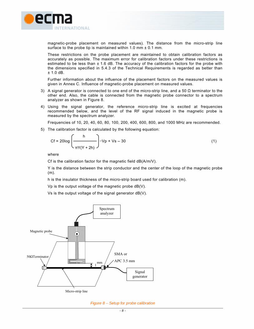
2) As an example, a setup of the magnetic probe calibration is shown in Figure 8. The magnetic probe is placed over the micro-strip lines in such a way that the plane of the loop is perpendicular to the ground plane and parallel to the longitudinal axis of the micro-strip line. The center of the probe is located within ± 0.4 mm (horizontal displacement) from the center of the micro-strip line. The face angle of the probe is within a 5º deviation from the axis of the micro-strip line, in order to keep the deviation within 0.2 dB (Refer to Annex C. Influence of
W (1.0 mm)
h (0.6 mm)
Wg (50 mm or more)
Strip line
Ground
Insulator (ε r=4.7)
- 8 -
magnetic-probe placement on measured values). The distance from the micro-strip line surface to the probe tip is maintained within 1.0 mm ± 0.1 mm.
These restrictions on the probe placement are maintained to obtain calibration factors as accurately as possible. The maximum error for calibration factors under these restrictions is estimated to be less than ± 1.6 dB. The accuracy of the calibration factors for the probe with the dimensions specified in 5.4.3 of the Technical Requirements is regarded as better than ± 1.0 dB.
Further information about the influence of the placement factors on the measured values is given in Annex C. Influence of magnetic-probe placement on measured values.
3) A signal generator is connected to one end of the micro-strip line, and a 50 Ω terminator to the other end. Also, the cable is connected from the magnetic probe connector to a spectrum analyzer as shown in Figure 8.
4) Using the signal generator, the reference micro-strip line is excited at frequencies recommended below, and the level of the RF signal induced in the magnetic probe is measured by the spectrum analyzer.
Frequencies of 10, 20, 40, 60, 80, 100, 200, 400, 600, 800, and 1000 MHz are recommended.
5) The calibration factor is calculated by the following equation:
h Cf = 20log —Vp + Vs – 30 (1)
πY(Y + 2h)
where
Cf is the calibration factor for the magnetic field dB(A/m/V).
Y is the distance between the strip conductor and the center of the loop of the magnetic probe (m).
h is the insulator thickness of the micro-strip board used for calibration (m).
Vp is the output voltage of the magnetic probe dB(V).
Vs is the output voltage of the signal generator dB(V).
Figure 8 – Setup for probe calibration
1 mm
50ΩTerminator
Spectrum analyzer
Signal generator
Magnetic probe
Micro-strip line
SMA or
APC 3.5 mm

- 9 -
Annex A
Conditions for measuring emissions from the Module Under Test
This Annex supplements Clause 6. It includes the placement and the operating conditions of the module as a MUT to obtain a higher repeatability of the measurement.
The test board consists of a control circuit and a power supply; it is required to operate the MUT as a single unit; the printed circuit feeding the MUT contains a micro-strip line for measuring the current to the MUT with a magnetic probe.
A.1 Test board
A.1.1 Layer placement The test board should have a multi-layer structure composed of four layers or more. Additional layers may be inserted between the bottom layer and the ground plane to accommodate additional signal and/or power routing, as required.
1) Layer 1
The MUT shall be put on layer 1. The power supply line for measurement and the peripheral ground planes shall be placed on this plane. With this power supply line pattern, each power line shall be constructed in accordance with Figure A.1. The regular width of the power supply line will be 1.0 mm to achieve a high spatial resolution. If the regular line width lacks current capacity, you can change the line width of the micro-strip line. For details, refer to Annex B.
The length of the power supply line (in Figure A.1, the distance from the center of the via to VDD land to the 0.1 µF decoupling capacitor) shall be a maximum of 25 mm to avoid standing waves.
2) Layer 2
A ground plane area shall be formed to provide a reference for the micro-strip structures on layer 1. The ground plane can cover the entire layer or can be limited to the area under the micro-strip structures, shown in the dotted-line area of Figure A.1. The ground plane area shall have a minimum width of 11 mm and a minimum length of 14 mm.
3) Layer 3
A power supply pattern for the control circuit shall be placed.
4) Layer 4
A pattern for the signal lines shall be placed.
5) Impedance of power supply lines (measuring lines)
The thickness of the insulator between layers 1 and 2 of the printed circuit shall be 0.6 mm or less. The distance between strip line in layer 1 and ground plane shall be 2.0 mm or greater. If the thickness of the insulator is changed, the impedance shall be calculated by using the coupling factor shown in Figure B.2.

- 10 -
Figure A.1 – Power line pattern on the test board (layer 1)
A.1.2 Decoupling capacitor A decoupling capacitor (C2) shall be used between the power supply lines and ground planes on the test board as shown in Figure A.1. The capacitor C2 shall be placed as close as possible to the measurement area of the power supply line to provide low RF impedance.
A.1.3 Other components All other components shall be placed on the bottom layer. These components shall not be placed in the dotted-line area in Figure A.1.
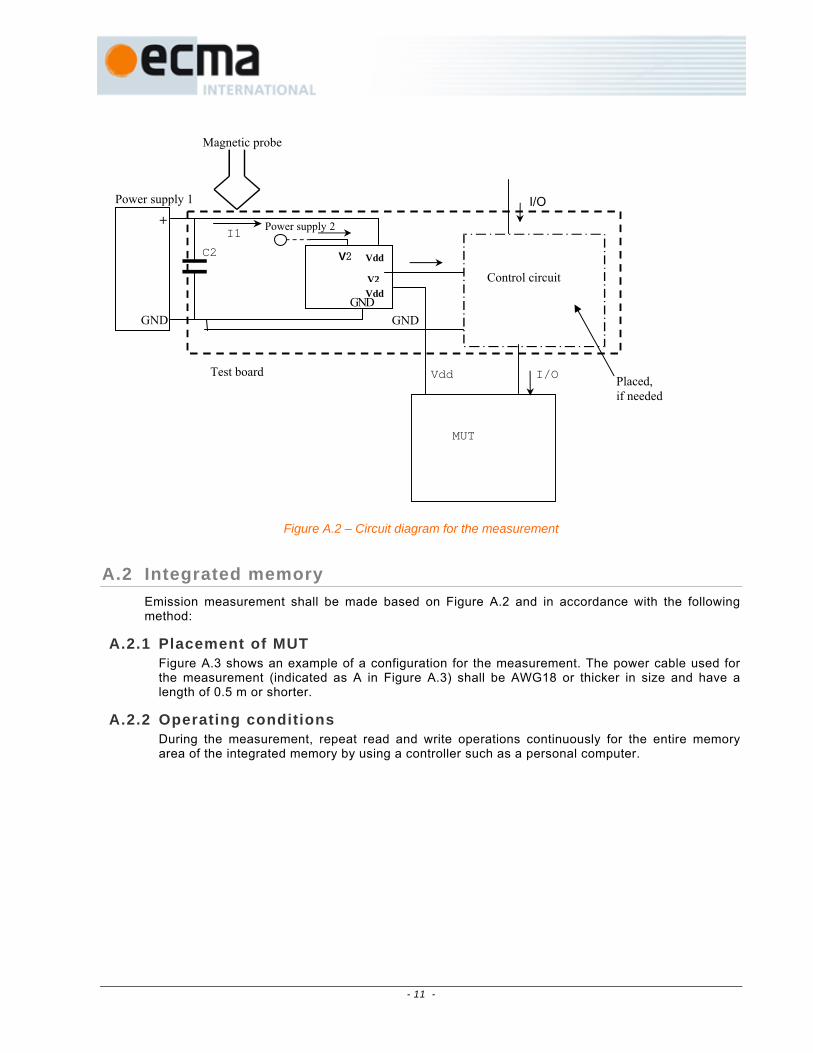
A.1.4 Measuring circuit Figure A.2 shows the circuit diagram to measure emission current (I1) emitted from the MUT, by use of the magnetic probe.
m
in. 1
4 m
m
Via to Vdd pad for DUT: 0.8 mm diameter
Coplanar gap : 2.0 mm min.
Power supply strip width : 1.0 mm max.
Via : 0.8 mm diameter
Layer 2 : Ground plane
Decoupling capacitor (0.1μF)
Decoupling capacitor (10μF)
Power supply pad
Overlapped plane width between layer 1 and layer 2 ground plane : 3.0 mm min.
C2
max
. 25
mm
Peripheral ground plane
min.11 mm
- 11 -
Figure A.2 – Circuit diagram for the measurement
A.2 Integrated memory Emission measurement shall be made based on Figure A.2 and in accordance with the following method:
A.2.1 Placement of MUT Figure A.3 shows an example of a configuration for the measurement. The power cable used for the measurement (indicated as A in Figure A.3) shall be AWG18 or thicker in size and have a length of 0.5 m or shorter.
A.2.2 Operating conditions During the measurement, repeat read and write operations continuously for the entire memory area of the integrated memory by using a controller such as a personal computer.
GND
C2
Magnetic probe
Power supply 1
+
GND GND
I1
I I/O対向
器
V2
Power supply 2
Vdd
Control circuit
Placed, if needed
V2Vdd
I/O
I/OVdd
MUT
Test board
- 12 -
Components
No. Name
① MUT
② Test board
③ Power supply connector
④ Connector for MUT
⑤ Controller
⑥ Regulated power supply
Cable
No. Cable Wire size Length (m)
A Power supply cable AWG18 or thicker in size 0.50 or less
Figure A.3 – Configuration example for measuring emission from integrated memory
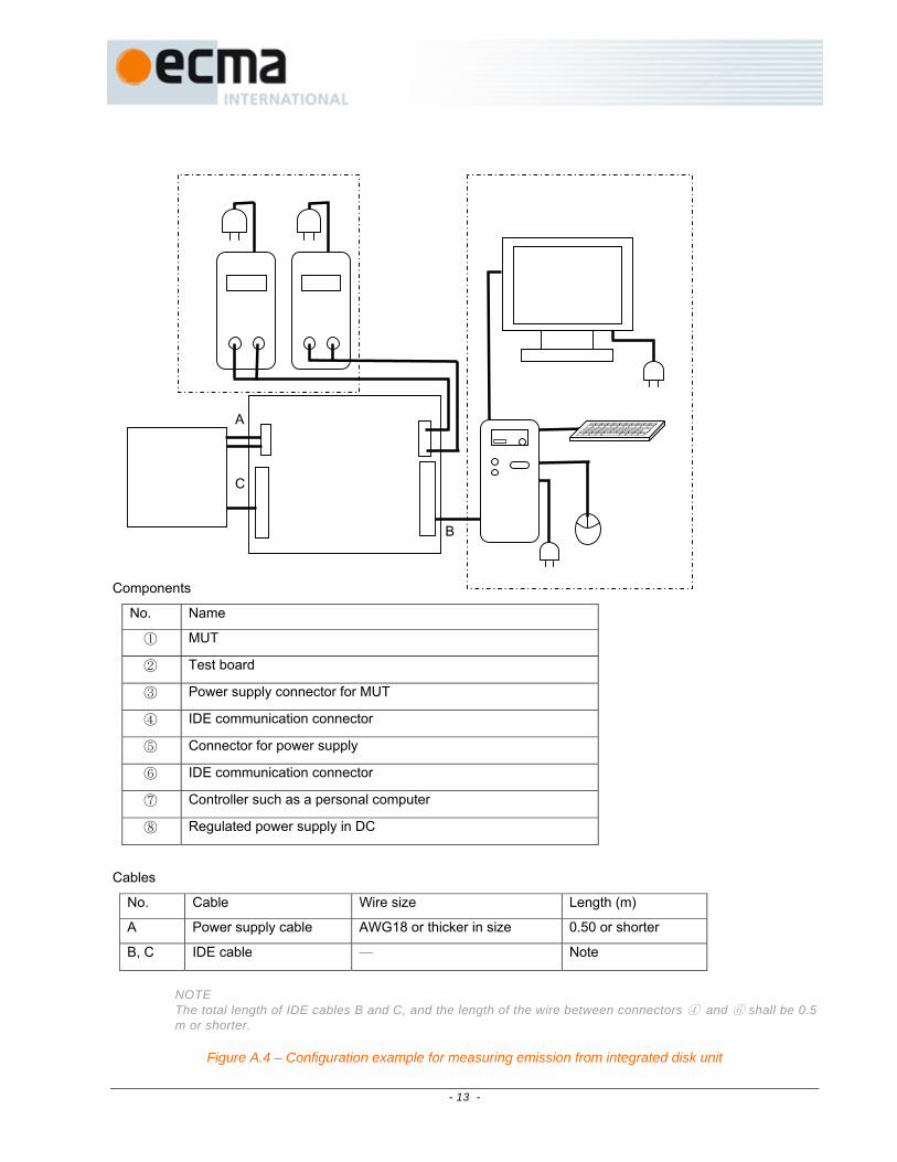
A.3 Integrated disk unit Emission measurement shall be made based on Figure A.2 and in accordance with the following method:
A.3.1 Placement of MUT Figure A.4 shows an example of a configuration for the measurement. The power cable used for the measurement (indicated as A in Figure A.4) shall be AWG18 or thicker in size, and shall have a length of 0.5 m or shorter. The total length of IDE cables B and C, and the length of the wire between connectors ④ and ⑥ shall be 0.5 m or shorter.
A.3.2 Operating conditions During the measurement, repeat read and write operations continuously for the entire data area of the integrated disk unit by using a controller such as a personal computer.
A
- 13 -
Components
No. Name
① MUT
② Test board
③ Power supply connector for MUT
④ IDE communication connector
⑤ Connector for power supply
⑥ IDE communication connector
⑦ Controller such as a personal computer
⑧ Regulated power supply in DC
Cables
No. Cable Wire size Length (m)
A Power supply cable AWG18 or thicker in size 0.50 or shorter
B, C IDE cable ― Note
NOTE The total length of IDE cables B and C, and the length of the wire between connectors ④ and ⑥ shall be 0.5 m or shorter.
Figure A.4 – Configuration example for measuring emission from integrated disk unit
B
A
C

- 14 -
A.4 Interface board Emission measurement shall be made based on Figure A.2 and in accordance with the following method:
A.4.1 Placement of MUT Figure A.5 shows an example of a configuration for the measurement. The LAN cable used for the measurement (indicated as A in Figure A.5) shall be 3 m or shorter, and the interface cable (indicated as B in Figure A.5) shall be 0.4 m or shorter.
A.4.2 Operating conditions During the measurement, repeat the data communication or read and write operations continuously by using a controller such as a personal computer.

- 15 -
Components
No. Name
① MUT
② Test board
③ Interface connector
④ Controller such as a personal computer
⑤ Corresponding unit such as a personal computer
Cables
No. Cable length (m)
A LAN cable 3.00 or shorter
B Interface cable
0.40 or shorter
Figure A.5 – Configuration example for measuring emission from interface board
B
A

- 16 -

- 17 -
Annex B
Current measurements with a magnetic probe
The output voltage Vp of the shielded-loop type magnetic probe described in the Technical Requirements 4.3.3 can be measured with a measuring receiver or a spectrum analyzer.
Magnetic field Hx can be calculated from measured value Vp and the calibration factor Cf of the magnetic probe by use of the following equation:
Hx = Cf + Vp (1)
Then, using the coupling factor Ch of the test board, we obtain the RF current I from the following equation:
I = Vp + Cf – Ch (2)
where
Hx is the magnetic field dB(A/m).
I is the RF current dB(A).
Vp is the output voltage of the magnetic probe dB(V).
Cf is the calibration factor of the magnetic probe dB(A/m/V).
Ch is the coupling factor of the test board dB(1/m).
(Calibration factor: Cf)
An example of the calibration factor of the shielded-loop type magnetic probe described in the Technical Requirements 4.3.3 is shown in Figure B.1.
0
20
40
60
80
100
0.1 1.0 10.0 100.0 1000.0Frequency [MHz]
Cal
ibra
tion
fact
or C
f [dB
A/m
/V]
Figure B.1 – An example of Measurement of the calibration factor of the magnetic probe

- 18 -
(Coupling factor: Cn)
The coupling factor Ch varies depending on the thickness of the insulation between layers 1 and 2 of the test board, as Figure B.2 shows. For the recommended insulation thickness h = 0.6 mm, the coupling factor is 30 dB/m. For the test board in which the insulation thickness is not 0.6 mm, we can calculate the RF current by using an adequate coupling factor Ch from Figure B.2, and following the equation (2).
Figure B.2 – Relation of insulation thickness between layer 1 and 2 of test board with coupling factor
If the specified power supply strip line width: 1mm in Supplement 1-1 is insufficient for the current capacity, strip line width can be expanded. In that case, you should use the line width w, the thickness h between layers, and the coupling factor Ch shown in Table B.1. Table B.1 shows the cases when the conductor thickness of the micro-strip line is 35 µm, and the resist thickness is 20 µm.
Table B.1 – Coupling factors for the expanded str ip l ine width
Line width (mm) Thickness h between layers 1 and 2 (mm)
Coupling factor Ch dB(1/m)
2 0.1 17
0.6 29
5 0.1 11
0.6 24
Where, the conductor thickness of the micro-strip line is 35 µm, and the resist thickness is 20 µm.
Cou
plin
g fa
ctor
Ch
[dB
1/m
]
Thickness of insulator h[mm]

- 19 -
Annex C
Influence of magnetic-probe placement on measured values
The diagram for measuring the magnetic field distribution across a micro-strip line is shown in Figure C.1. Figure C.2 is the characteristic curve that shows the spatial resolution of the shielded-loop type magnetic probe described in 4.3.3 of the Technical Requirements.
When the height of the magnetic probe is fixed at 1 mm from the conductor surface, the spatial resolution at 800 MHz is about 1.2 mm (−6 dB drop point). Therefore, if the height of the magnetic probe is fixed at 1 mm from the conductor surface, and the space between two adjacent conductors on the test board used for the emission measurement is about 2 mm, the magnetic field from adjacent conductors gives little influence. Therefore, we consider that the error in the measurement can be neglected.
Figure C.1 – Diagram for measuring a magnetic field distribution
Figure C.2 – Magnetic field distribution over the micro-strip line (at 800 MHz)
-40 -3 -2 -1 0 1 2 3
Position x [mm]
x = 0 (0 dB) x
1.0 mm
0.6 mm
1.0 mm
Magnetic probe
Out
put o
f mag
netic
pro
be (d
B)
-30
-20
-10 -6 0

- 20 -
A measurement error might be caused due to an inadequate placement angle of the magnetic probe to the direction of the micro-strip line under measurement.
The diagram for testing the influence of the placement angle ψ of the magnetic probe with respect to the direction of a micro-strip line is shown in Figure C.3.
Figure C.3 – Diagram for measuring an angle pattern for probe placement
We understand that the output voltage of the shielded-loop type magnetic probe changes depending on the probe placement angle ψ to the direction of a micro-strip line under measurement, as Figure C.4 shows. Therefore, in order to accurately measure the current in the micro-strip line by using the shielded-loop type magnetic probe, it is required to place the magnetic probe in such a manner that the angle ψ in Figure C.3 is less than 5 degrees and as least as possible.
Figure C.4 – Probe output to angle
-2
-1
0
0 5 10 15Placement angle ψ
Out
put o
f mag
netic
pro
be (d
B)
ψ
Magnetic
Micro-strip line