ecse-426 microprocessor systems - simon foucher's … microp/lectures/l3.pdflecture 3 3...
TRANSCRIPT
Lecture 3 1
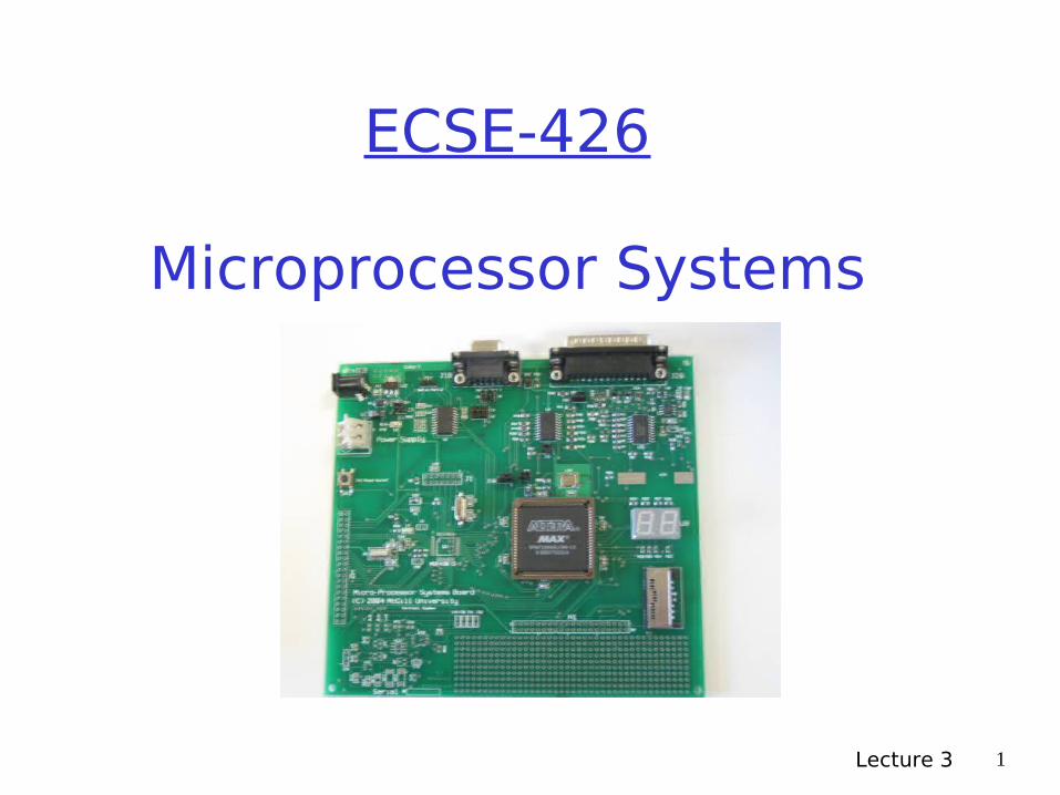
ECSE-426
Microprocessor Systems

Lecture 3 2
Deadline extended to Sunday, Sept 20th at midnight Give you a bit more time outside the weekdays.
Electronic copy (.PDF) will be accepted No paper copy is needed if you use this method A single, self-contained PDF document
• Experiment data and source code in Appendix PDF ONLY (no .DOC, .DOCX, .ODT, etc.) Submit the electronic copy through WebCT before the
deadline.
You can also submit a paper report in the assignment box
This is the alternate option for those who cannot output a PDF or if you wrote it all by hand.
Lab 1 Experiment Report

Lecture 3 3
Today’s Lecture
Theory ISA
• Addressing Modes• Bytes/Bits ordering
Interrupts
Practical Information (MSP430) Clocks Interrupts Timers Digital I/O
Lecture 3 4
Instruction Set Architecture
Recall : Abstraction of the Microarchitecture Level Provide a functional, detailed view of the processor Abstracts out microprogram details and implementation
Allows new implementations to be backward compatible with older designs
Multiple implementations of the same ISA• E.g. Pipelined vs non-pipelined core
Allows tradeoffs to be done at the hardware level• Keeping the compiler maintainers, OS sw, users happy
The ISA is usually defined in a specific document E.g. MSP430 User Guide Consistent for all the MSP430 family.

Lecture 3 5
Example : ARM Cortex-M3
Cortex-M3 Thumb2 instructions
Low-costs embedded targets 32-bit registers, 16-bit instruction set 3-stage pipeline, Harvard architecture Atomic bit manipulation
• Read-modify-write in one operation (indivisible)• Useful in embedded systems• Allows concurrent access to shared elements

Lecture 3 6
ARM Cortex-M3 (ctd.) Sixteen 32-bit registers Note the banking of Stack Pointer (SP) LR : Link Register.
Holds the return address for leaf function call
Source: ARM Cortex-M3 Technical Reference Manual – r2p0, Section 2-4

Lecture 3 7
IA-32 Architecture EAX — Accumulator for operands and
results data EBX — Pointer to data in the DS segment ECX — Counter for string and loop
operations EDX — I/O pointer ESI — Pointer to data in the segment
pointed to by the DS register; source pointer for string operations
EDI — Pointer to data (or destination) in the segment pointed to by the ES register; destination pointer for string operations
ESP — Stack pointer (in the SS segment) Segments allow different areas of memory to
have protection. It allows hardware to intercept invalid/forbidden operations.
Source : Intel® 64 and IA-32 Architectures Software Developer’s Manual Volume 1

Lecture 3 8
IA32 Architecture – BCD BCD Integer – One BCD digit per byte Packed BCD – 2 BCD digits per byte For the co-processor:
80-Bit Packed BCD in memory are converted to extended double-precision floating point when used by the co-processor
Binary operations on BCD, then adjustment Instructions to recover proper BCD (E.g : DAA)
ADD + DAA : Decimal adjust after addition SUB + DAS : Decimal adjust after substraction

Lecture 3 9
IA32 Architecture - SIMD
Single Instruction Multiple Data (SIMD) MMX, SSE, SSE2, SSSE2 Manipulate many smaller data units in one instruction Useful for graphics, DSP and other media applications
Operate on packed data formats Horizontal repetition of the same data type
• E.g. Packed Bytes => 16 bytes in a 128-bit register• One instruction is equivalent to 16 independent operations
on the byte fields, but all in one operation Example :
• Add Packed Unsigned Integers with Unsigned Saturation• PADDUSB xmm1,xmm2/m128

Lecture 3 10
PADDUSB Example PADDUSB instruction with 128-bit operands:
DEST[7:0] ← SaturateToUnsignedByte (DEST[7:0] + SRC[7:0]); (* Repeat add operation for 2nd through 14th bytes *) DEST[127:120] ← SaturateToUnSignedByte (DEST[127:120] +
SRC[127:120]);
Operates on XMM Registers (SSE2, SSE3, SSSE3) Core2 architecture, for example.
Lecture 3 11
ISA – Summary
The Instruction Set Architecture defines what the programmer can do with the machine
Stable foundations to build compilers, libraries, etc.
ISA vary among architectures and within a line of product
Share some common registers/operations More $$$ => more specialized instructions/coprocessor
Difficult to compare architectures Million instructions per second (MIPS)... 1 MIPS of MSP430 clearly not equal to 1 MIPS of SSE3 Marketing ?
Lecture 3 12
Addressing Modes Immediate
All the required information is part of the instruction E.g. MOV #4, R5
Direct (Absolute) From a fixed location in memory E.g. MOV &Label, R5
Register Indirect Using a register content as a pointer E.g. MOV @R5, R6 ; R5 contains a valid address
Register Mode Manipulate registers only E.g. MOV R5,R6
Note : MOV width should be specified (MOV.B or MOV.W)

Lecture 3 13
Addressing Modes (ctd.) Indexed
Similar to Indirect Register Mode, but with offset MOV 4(SP), R5
• R5 will contain the value at address SP+4
Symbolic Mode Similar to Direct Addressing Mode Except that the symbol is an offset from the PC E.g. MOV Label, R5
Indirect with Autoincrement Adds automatic increment of pointers Faster memory copy, array scanning, etc. E.g. MOV @R5+, R6

Lecture 3 14
Assembly Addressing modes
MSP430
MODE NAME FORMAT OPERAND
Register mode Rn Register Contents
Indexed mode X(Rn) (Rn+X) points to operandSymbolic mode ADDR (PC+X) points to operandAbsolute mode &ADDR ADDR is abs. addressIndirect register @Rn Rn is a pointer to operandIndirect autoinc. @Rn+Immediate mode #N use immediate constant N

Lecture 3 15
Bits and Bytes Ordering
How many ways can it be done ?
Lecture 3 16
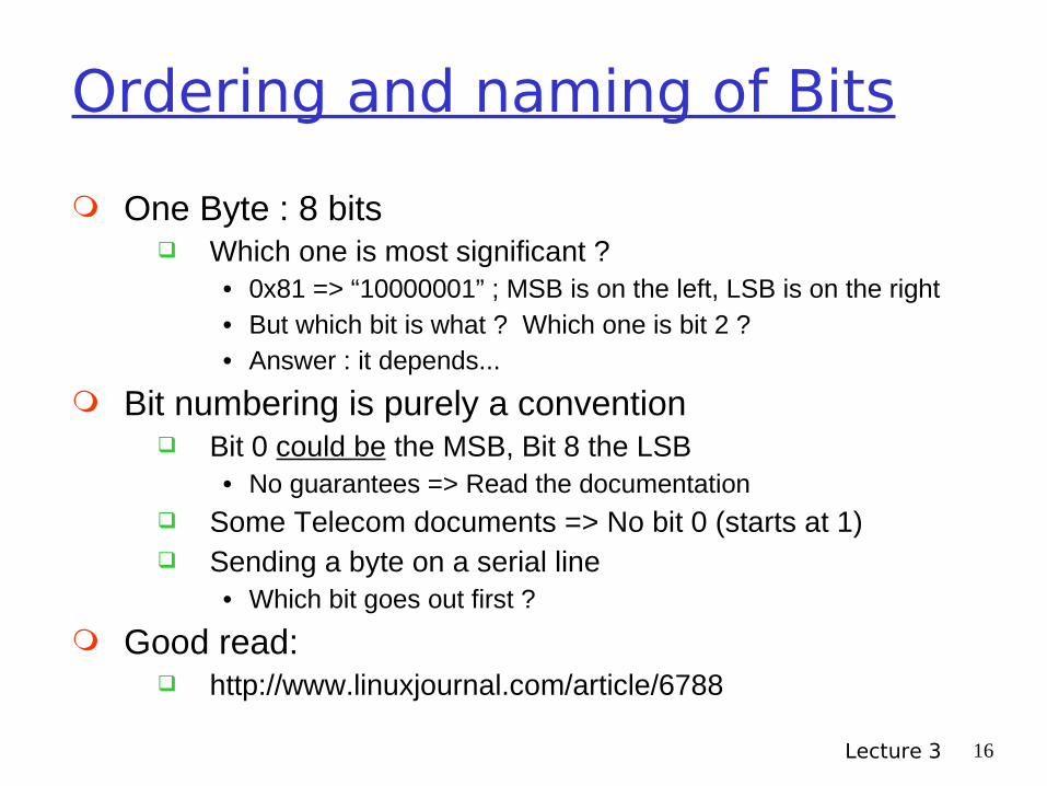
Ordering and naming of Bits
One Byte : 8 bits Which one is most significant ?
• 0x81 => “10000001” ; MSB is on the left, LSB is on the right• But which bit is what ? Which one is bit 2 ?• Answer : it depends...
Bit numbering is purely a convention Bit 0 could be the MSB, Bit 8 the LSB
• No guarantees => Read the documentation Some Telecom documents => No bit 0 (starts at 1) Sending a byte on a serial line
• Which bit goes out first ?
Good read: http://www.linuxjournal.com/article/6788

Lecture 3 17
Byte Ordering
Little Endian vs Big Endian Intel, AMD, MSP430 => Little Endian PowerPC, Motorola => Big Endian ARM, MIPS => Programmable (Either one)
0x0a0b0c0d (example 32-bit number) Big Endian
Little Endian
Endianness of various parts in a system CPU, BUS, Device, Network
byte addr 0 1 2 3bit offset 01234567 01234567 01234567 01234567 binary 00001010 00001011 00001100 00001101 hex 0a 0b 0c 0d
byte addr 3 2 1 0bit offset 76543210 76543210 76543210 76543210 binary 00001010 00001011 00001100 00001101 hex 0a 0b 0c 0d
Example taken from : http://www.linuxjournal.com/article/6788
Lecture 3 18
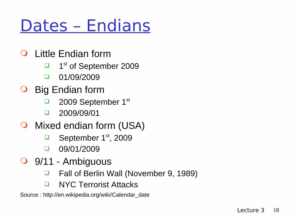
Dates – Endians
Little Endian form 1st of September 2009 01/09/2009
Big Endian form 2009 September 1st
2009/09/01
Mixed endian form (USA) September 1st, 2009 09/01/2009
9/11 - Ambiguous Fall of Berlin Wall (November 9, 1989) NYC Terrorist Attacks
Source : http://en.wikipedia.org/wiki/Calendar_date

Lecture 3 19
Interrupts
Hardware event (some software exceptions) triggers the processor to jump from its current program
counter to a specific point in the code. Unpredictable special events
Each interrupt Assigned word long segment at upper end of memory
• Jump to location where interrupt is handled
Maskable: programmer can decide if the interrupt causes a jump
Non-maskable interrupt (like the reset button) is so important that it should never be ignored.
Lecture 3 20
Interrupts (2)
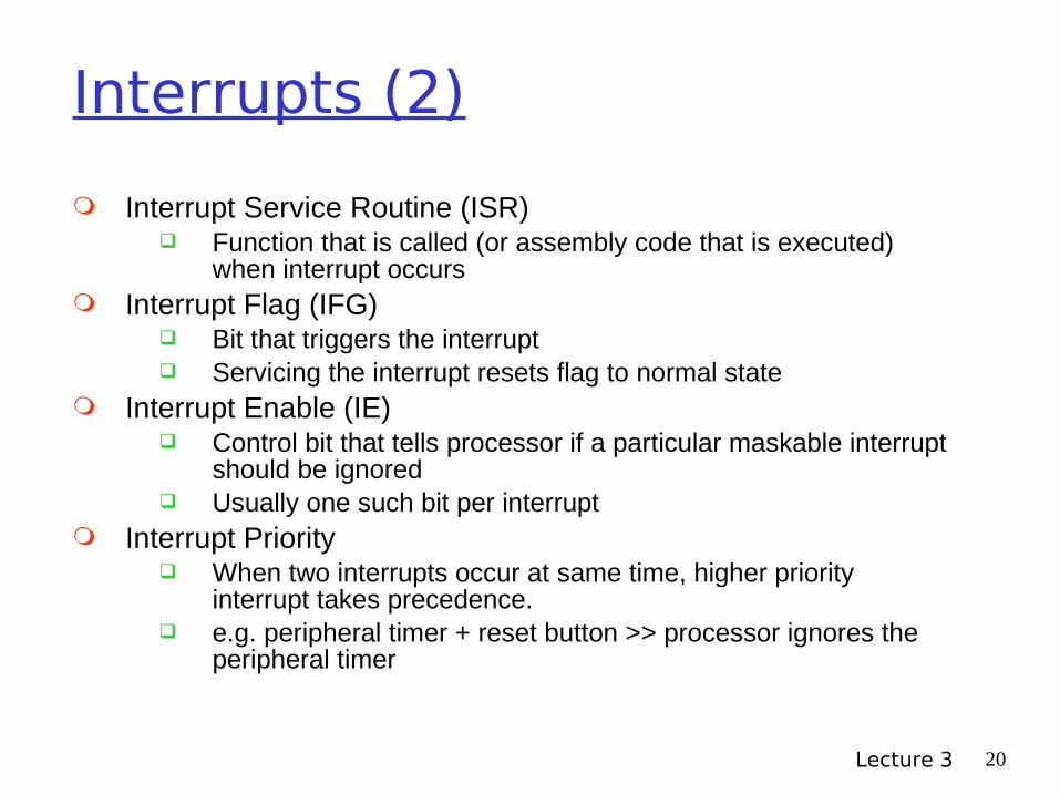
Interrupt Service Routine (ISR) Function that is called (or assembly code that is executed)
when interrupt occurs Interrupt Flag (IFG)
Bit that triggers the interrupt Servicing the interrupt resets flag to normal state
Interrupt Enable (IE) Control bit that tells processor if a particular maskable interrupt
should be ignored Usually one such bit per interrupt
Interrupt Priority When two interrupts occur at same time, higher priority
interrupt takes precedence. e.g. peripheral timer + reset button >> processor ignores the
peripheral timer
Lecture 3 21
Interrupts
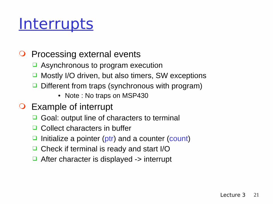
Processing external events Asynchronous to program execution Mostly I/O driven, but also timers, SW exceptions Different from traps (synchronous with program)
• Note : No traps on MSP430
Example of interrupt Goal: output line of characters to terminal Collect characters in buffer Initialize a pointer (ptr) and a counter (count) Check if terminal is ready and start I/O After character is displayed -> interrupt
Lecture 3 22
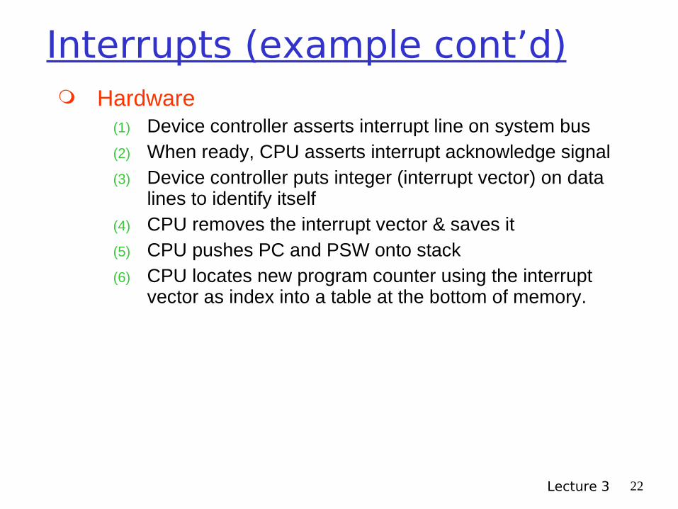
Interrupts (example cont’d) Hardware
(1) Device controller asserts interrupt line on system bus(2) When ready, CPU asserts interrupt acknowledge signal(3) Device controller puts integer (interrupt vector) on data
lines to identify itself(4) CPU removes the interrupt vector & saves it(5) CPU pushes PC and PSW onto stack(6) CPU locates new program counter using the interrupt
vector as index into a table at the bottom of memory.

Lecture 3 23
Interrupts (example cont’d) Software
(1) Interrupt service routine saves all registers(2) Read device register to determine terminal number(3) Read status codes for the interrupt(4) Handle a potential I/O error(5) Increment ptr, decrement count. If count > 0, copy *ptr to
output register(6) If required, output special code to tell device or interrupt
controller that interrupt has been processed(7) Restore all saved registers.(8) Execute the return from interrupt (RETI) instruction, restoring
state/mode of CPU.
Note : C Compilers will take care of saving / restoring the context.
Lecture 3 24
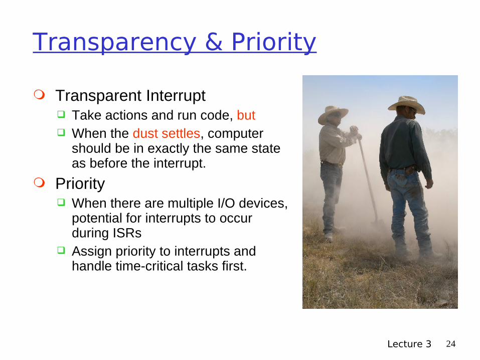
Transparency & Priority
Transparent Interrupt Take actions and run code, but When the dust settles, computer
should be in exactly the same state as before the interrupt.
Priority When there are multiple I/O devices,
potential for interrupts to occur during ISRs
Assign priority to interrupts and handle time-critical tasks first.
Lecture 3 25
Small Interlude
A few minutes Any questions on the lab ? Do you all have your kits ? Tutorial today (?) and tomorrow
• Check WebCT for the details
Next : Practical info on MSP430 MSP430
• Clocks• Timers• Interrupts• Digital I/O

Lecture 3 26
MSP430 Clocks
Three clock sources and three clock lines – allows a mix of slow and fast clocks in the system.
Low Frequency Crystal Clock (LFXTCLK) – Crystal connected to the XIN and XOUT pins with intended
oscillation of 32kHz. Always the source of the Auxiliary Clock line (ACLK). This source can be turned off with the OSCOFF option in the
Status Register.
Crystal 2 Clock (XT2CLK) – 8 MHz crystal connected to the XT2IN and XT2OUT pins. In general, this signal is meant to be the high-speed clock
source. This source can be turned off with the XT2OFF bit of the Basic
Clock system control register 1 (BCSCTL1).

Lecture 3 27
MSP430 Clocks (ctd)
Digitally Controlled Oscillator Clock (DCOCLK) the only internally generated clock input default clock source for the master clock upon reset. By default this clock runs at about 900kHZ The RSELx, MODx, and DCOx bits allow adjustment
Lecture 3 28
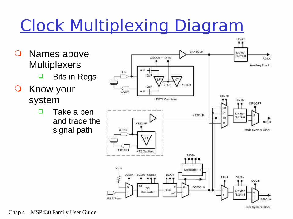
Clock Multiplexing Diagram
Names above Multiplexers
Bits in Regs
Know your system
Take a pen and trace the signal path
Chap 4 – MSP430 Family User Guide

Lecture 3 29
Example – MCLK Selection

Lecture 3 30
MSP430 Clock Lines
Master Clock (MCLK) Source for the MSP CPU core; Must be working properly for the processor to execute
instructions. Source is selected with the SELMx bits of the Basic Clock
System Control Register 2 (BCSCTL2). The divider is controlled with the DIVMx of the BCSCTL2. CPU can be turned off with the CPUOFF bit of the Status
Register (SR), but to recover from this state an interrupt must occur.
# Submaster Clock (SMCLK) - This clock is the source for most peripherals, and its source can either be the DCO or Crystal 2. The source clock is controlled with the SELS and SCG bits of the BCSCTL2 and SR. The divider is controlled by the DIVSx bits of the BCSCTL2.

Lecture 3 31
MSP430 Clock Lines (ctd)
# Auxiliary Clock (ACLK) - this clock line’s source is always LFXTCLK. It is an option for slower subsystems to use in order to conserve power. This clock can be divided as controlled by the DIVAx bits of the Basic Clock System Control Register 1 (BCSCTL1).

Lecture 3 32
Timers
Two digital timers, A & B. Timer A:
3 capture/compare registers Interrupts: via overflow, or from one of the capture/compare
registers. Selectable clock source Configurable outputs with PWM (pulse-width modulated)
capability Interval timing

Lecture 3 33
Timer A
16 bit timer/counter register, TAR increments/decrements with each rising edge of clock Software read/write Interrupt on overflow. Clear: TACLR bit (also clears clock divider and count
direction)
Clock source ACLK, SMCLK, or externally (TACLK or INCLK)

Lecture 3 34
Timer A
Start timer MCx > 0 and clock source active In up or up/down mode
• write 0 to TACCR0 to stop timer• then write nonzero value to TACCR0 to start.
Modes Stop: timer halted Up: zero to TACCR0 repeatedly Continuous: zero to 0xFFFFh Up/down: zero to TACCRO, back to zero

Lecture 3 35
Timer A Modes
Up mode: Used for periods different from 0xFFFFh Timer counts per period is TACCR0+1 TACCR0 CCIFG interrupt flag set when timer counts to
TACCR0 value TAIFG flag when timer counts to zero
Continuous mode TAIFG flag set when timer counts from 0xFFFFh to 0
Lecture 3 36
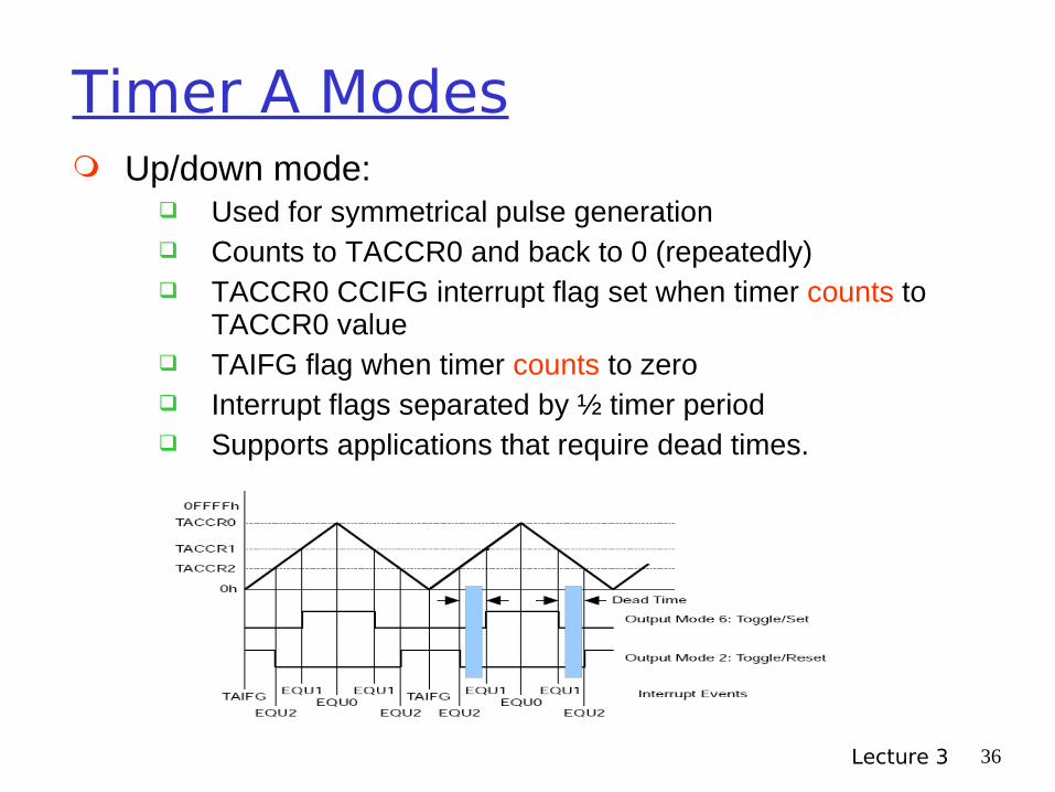
Timer A Modes Up/down mode:
Used for symmetrical pulse generation Counts to TACCR0 and back to 0 (repeatedly) TACCR0 CCIFG interrupt flag set when timer counts to
TACCR0 value TAIFG flag when timer counts to zero Interrupt flags separated by ½ timer period Supports applications that require dead times.
Lecture 3 37
Capture/compare blocks
Capture mode (CAP = 0) Used to record time events (speed computations, time
measurements) Capture occurs on selected edge of input
• Timer value copied to TACCRx register• Interrupt flag CCIFG is set
Compare mode (CAP = 1) Used to generate PWM output signals or interrupts at
specific time intervals When TAR counts to TACCRx
• Set CCIFG, set internal signal EQUx = 1, latch CCI to SCCI.
Lecture 3 38
Timer A Interrupts
Two interrupt vectors TACCR0 vector for TACCR0 CCIFG TAIV vector for all other CCIFG flags and TAIFG.
In capture mode, a CCIFG flag is set when a time value is captured. In compare mode, a CCIFG flag is set if TAR counts to the associated TACCRx value.
TACCR0 CCIFG : highest priority Dedicated interrupt vector
Lecture 3 39
Timer A Interrupts
TAIV vector - prioritized(1) TACCR1 CCIFG(2) TACCR2 CCIFG(3) TAIFG (overflow flag)

Lecture 3 40
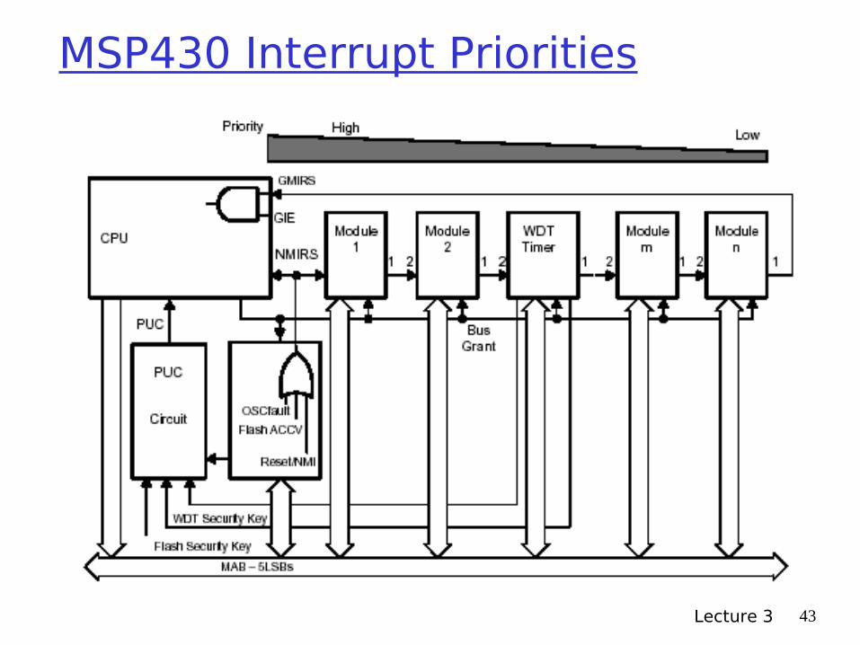
MSP430 Interrupt Mechanisms Peripheral devices
USART, Timers, AD/DA, GPIO
Pins NMI, Reset, P.0, P.1
A daisy chain of requestors On MSP430:
Closer to processor, the higher priority Power-up : highest priority See priority table (datasheet).

Lecture 3 41
MSP430 Interrupt Mechanisms

Lecture 3 42
MSP430 Interrupt Processing Table definition:
Lecture 3 43
MSP430 Interrupt Priorities
Lecture 3 44
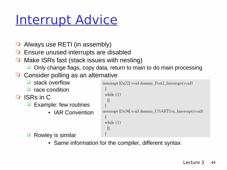
Interrupt Advice
Always use RETI (in assembly) Ensure unused interrupts are disabled Make ISRs fast (stack issues with nesting)
Only change flags, copy data, return to main to do main processing Consider polling as an alternative
stack overflow race condition
ISRs in C Example: few routines
• IAR Convention
Rowley is similar• Same information for the compiler, different syntax
Lecture 3 45
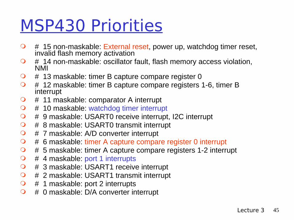
MSP430 Priorities # 15 non-maskable: External reset, power up, watchdog timer reset,
invalid flash memory activation # 14 non-maskable: oscillator fault, flash memory access violation,
NMI # 13 maskable: timer B capture compare register 0 # 12 maskable: timer B capture compare registers 1-6, timer B
interrupt # 11 maskable: comparator A interrupt # 10 maskable: watchdog timer interrupt # 9 maskable: USART0 receive interrupt, I2C interrupt # 8 maskable: USART0 transmit interrupt # 7 maskable: A/D converter interrupt # 6 maskable: timer A capture compare register 0 interrupt # 5 maskable: timer A capture compare registers 1-2 interrupt # 4 maskable: port 1 interrupts # 3 maskable: USART1 receive interrupt # 2 maskable: USART1 transmit interrupt # 1 maskable: port 2 interrupts # 0 maskable: D/A converter interrupt
Lecture 3 46
Stack – Quick review
The stack is memory whose contents are kept in last in first out (LIFO) order.
Stack pointer is always updated to point to the most recent element added to the stack.
This allows the processor to call functions and track interrupts.
When something is pushed onto the stack, the stack pointer is incremented and the pushed data is written to that location.
When you copy out of the stack and decrement the stack pointer, this is called popping something off the stack.
Lecture 3 47
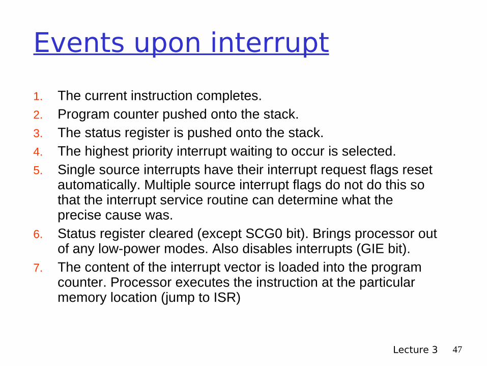
Events upon interrupt
1. The current instruction completes.2. Program counter pushed onto the stack. 3. The status register is pushed onto the stack.4. The highest priority interrupt waiting to occur is selected.5. Single source interrupts have their interrupt request flags reset
automatically. Multiple source interrupt flags do not do this so that the interrupt service routine can determine what the precise cause was.
6. Status register cleared (except SCG0 bit). Brings processor out of any low-power modes. Also disables interrupts (GIE bit).
7. The content of the interrupt vector is loaded into the program counter. Processor executes the instruction at the particular memory location (jump to ISR)

Lecture 3 48
ISR example Example: fet140_wdt01.c by Mark Buccini
// Watchdog Timer interrupt service routinevoid watchdog_timer(void) __interrupt[WDT_VECTOR] { P1OUT ^= 0x01; // Toggle P1.0 using exclusive-OR}
Always void (no arguments). Name does not matter. __interrupt[] is keyword indicating that routine is an interrupt WDT_VECTOR is macro from msp430 header file Every interrupt vector has a macro defined for it 5 cycles to exit: pop status register and all other settings + PC.
Lecture 3 49
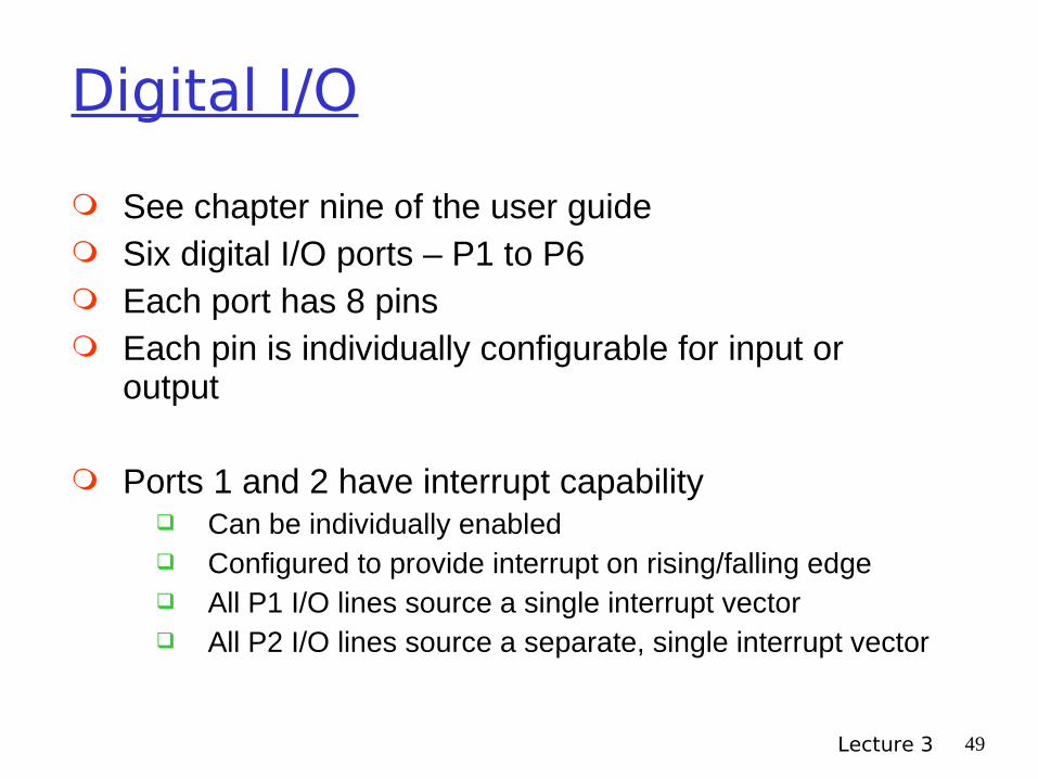
Digital I/O
See chapter nine of the user guide Six digital I/O ports – P1 to P6 Each port has 8 pins Each pin is individually configurable for input or
output
Ports 1 and 2 have interrupt capability Can be individually enabled Configured to provide interrupt on rising/falling edge All P1 I/O lines source a single interrupt vector All P2 I/O lines source a separate, single interrupt vector
Lecture 3 50
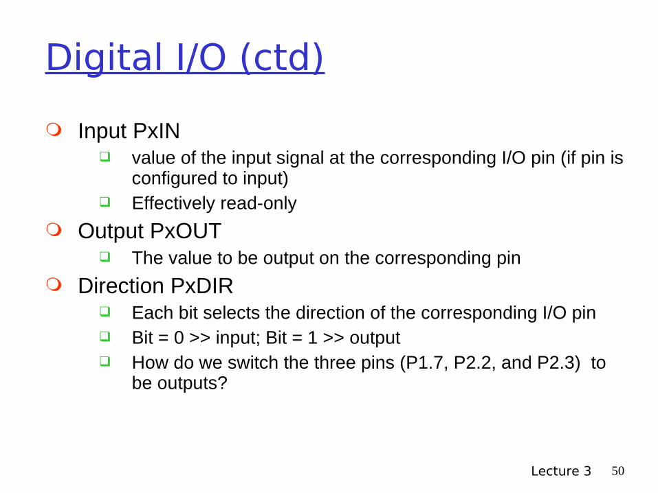
Digital I/O (ctd)
Input PxIN value of the input signal at the corresponding I/O pin (if pin is
configured to input) Effectively read-only
Output PxOUT The value to be output on the corresponding pin
Direction PxDIR Each bit selects the direction of the corresponding I/O pin Bit = 0 >> input; Bit = 1 >> output How do we switch the three pins (P1.7, P2.2, and P2.3) to
be outputs?

Lecture 3 51
Examples
Suppose three LEDs are connected to P1.7, P2.2 and P2.3. LEDs are turned on by setting their corresponding register bits
low.
How do we switch the three pins to be outputs?
How would be turn on the three LEDs without modifying any other bits in the register?
A button is connected to P2.0. The buttons are high (=1) by default and go low if the button is pressed.
Write a polling scheme for the button.

Lecture 3 52
Digital I/O (3) Pins can be multiplexed with other peripheral
module functions PxSELx – set to 0 to choose digital I/O and set to 1
to choose peripheral function
P1 and P2 interrupts PxIFG, PxIE and PxIES registers PxIFG register can be tested to determine the source of
a P1 or P2 interrupt (which pin). To enable interrupts, need to set the PxIE bit to 1 (and
the GIE bit) PxIES determines whether low-to-high transition or high-
to-low triggers interrupt Any external interrupt event should be at least 1.5 times
MCLK or longer
Lecture 3 53
Notes : Assembly Timing
Depends on addressing mode Each Type I and Type II instruction has a specified
number of cycles. Remember to allow for the time to enter and exit the
function if you are being precise in your timing.

Lecture 3 54
Your work this week
Complete Experiment 1 + Demo Get a MicroP Hardware Kit
Attend tutorial to know how to program it and how to use interrupts
Next Experiment will use hardware
Review Lecture 2 and Lecture 3 for the class Quiz Quiz is relatively easy if you listened in class and did the
Experiment.