edson d. de castro, president, data general...
TRANSCRIPT


Edson D. de Castro, President, Data General Corporation
A hard look at small computers Small computers are creating quite a stir.
. You hear that they are being purchased faster than any other kind of computer. And that they are creating an applications explosion, expanding even their current rate of sales growth.
It seems manufacturers have not let this action go unnoticed. The expanding marketplace is '
encouraging a rush of new products. Old designs are being revamped. New designs are being rushed to market. The mini-computer boom is on.
But what is the boom producing? Is a growing market and increasing competition producing better computer value ?
Well, the current crop of machines varies considerably. Word lengths vary. Input loutput facilities vary. Instruction sets vary. Software varies. Performance varies.
We designed the NOVA believing that new technology and improvements in the art of computer design had offered the opportunity for vast improvements in the price /performance ratio of the minimum configuration of small general purpose digital computers.
But there were some things we had to know before we could take advantage of these opportunities.
We had to know that, mini-computer or not, the power of these machines stems from their performance as general purpose computers. That whatever they are used for, they would have to be programmed h t . And that it was possible to so strip a computer of programming power that the machine could become more trouble than it was worth.
At the same time, we had to know that the special domain of these machines is in the on-line, real-time environment. That over half the small computers purchased are built into larger systems as special purpose data reducers and controllers.
I think you will find the NOVA to be a better small computer. We designed the system incorporating an architecture previously found only in medium and large scale third generation computers. This architecture permitted an extremely powerful instruction set. We took full advan!age of medium scale integration. We were also able to design the NOVA around the special input /output and packaging requirements of the small computer. We designed a new kind of read-only memory inter- changeable with core, for "black box" configurations.
You see, in designing and pricing the NOVA, we were after more than just getting a piece of the small computer action. We were after a machine that would be the basis for starting a major computer company.I think we succeeded. The NOVA is that good.


Richard G. Sogge, Vice President, Data General Corporation
The hardware As Ed has mentioned, the architecture of the NOVA had previously never been implemented in a
small computer design. The breakthrough that made it possible was medium scale integration. It now is possible to obtain sixteen flip-flops in a single package for use in regular registers; the
cost per function of an MSI component is somewhat lower than the cost of discrete gates and flip-flops. But that is not MSI's major contribution. The big savings with MSI came from the reduction of interconnection and resultant savings in packaging costs. And, of course, the reduction of inter- connection also had a very favorable effect on reliability. MSI accounts for over half the gates and flip-flops used in the NOVA.
And there are two kinds of memory available with the NOVA, core and read-only. A user will create his read-only memory by writing his program using a core memory. He uses the
full software of the system to write, edit, and debug his program. After he is satisfied with his program, he dumps it on paper tape and sends the tape to Data General. This tape is used as the basis for manufacturing the memory and verifying its contents. When complete, the read-only memory is simply plugged into the NOVA in place of the core memory. Should changes be required in the read-only memory they can easily be made by a technician.
These two kinds of memory are homogenous; the alterable and read-only storage are treated identically by the program and the processor. The only difference is that different kinds of memory vary in speed. But the two kinds of memory may be mixed. In a system in which only one program is being used, it can be stored along with its constants, in a read-only memory module. The alterable core memory can then be used for the storage of variable data and intermediary results. Or, the system con- sole can be removed and the system operated as a hard wired controller. By changing read-only memories, the functions performed by this controller may be altered. Memories are available in lK, 2K, or 4K word modules. The maximum memory size is 32K words or 64K bytes.
The read-write cycle times for the several core memory modules and the access time for read-only memory are as follows :
1K 6.5 micro-seconds 2K 3.9 4K 2.6 Read-only Memory 2.4
In and out Small computers interface with more kinds of devices with greater varying data rates and
priority interrupt requirements than any other class of computer. Not only do they interface with the full range of computer peripherals, but they often become part of special or unique systems.
We decided to build a complete input loutput facility into the basic NOVA. Included in the system are facilities for program interrupt and high speed data transfers with provision for direct access to memory. Any device can interrupt the normal program flow on a priority basis. A high speed device such as magnetic tape or disk can gain direct access to memory through a data channel without requir- ing the execution of any instructions. The data channel logic allows the transfer of data to or from memory, incrementing of memory word, and adding external data to a word already in memory. The latter two features facilitate such functions as signal averaging and pulse height analysis.
The NOVA 110facility consists of 16bi-directional data lines, 6 lines for device selection, 19 unary control lines from the central processor, and 6 control lines to the central processor. The control lines from the central processor are used to synchronize all data transfers on the data lines, to initiate and stop device functions, and to control the priority interrupt system. The control lines to the processor are used to indicate device status, and to request priority interrupt and data channel service.
The unary control lines from the processor contain two types of information: the specific function to be performed by the device, and timing information. These control lines are arranged in such a way that the device need connect only to those that correspond to the particular 110functions that the device requires. The timing of the control lines is determined by the processor in such a fashion that the device does not require any time-dependent circuits to connect to the I10 interface.
The input loutput system allows the program to address up to 62 external devices.


Henry Burkhardt, I l l , V ~ c ePres~dent,Data General Corporation
Instruction power Most medium and large scalethird generationcomputer systems have central processors
organizedaround multiple general purpose registers or accumulators.The logicaland arithmetic instructionsof these machines are performed by manipulating the contents of these accumulators.There is less need to addressor access memory.Also, the availablility of these multiple registers improves the efficiency of accumulatorto memory operationsand data flow between the computer and peripheral devices.
Until we designedthe NOVA, smallcomputerseither had a single accumulator or assigned mem-ory locationsto simulate this organization, tradingoff much of the basic power of the set-up.
In the NOVA we have been able to fullyimplement a multi-accumulatorcentral processor architecture.It is from this architecturethat much of the power of the machine stems.
The NOVA has four full sixteen-bit word accumulators, two of which may be used as index registers. Data can be moved in either directionbetween any memory location and any NOVA
..accumulator.Although a word in memory can be incremented or decremented, all other arithmetic and logical operationsare performed on operandsin the accumulators,with the result appearing in an accumulator. Associated with the accumulatorsis a single carry flag,whichindicateswhen the magnitude of the result is too large to be accommodated in a single accumulator. Theleft and right halves of any accumulatorcan be swapped, the contents of any accumulator can be tested for a skip,and the 17-bit word contained in any accumulator combined with the carry can be rotated right or left. An instruction that references memory can address two of the accumulators as index registers and transfers to and from peripheral devices are also made through the accumulators.
Thismulti-accumulator organization cuts down on the number of instructionsnecessary to executea program. And reduces the amount of data movement in the machine. For example, in as trivial an operation as the exchanging of the contents of two memory locations, the multi-accumulator set-up reduces the number of instructionsby one third.
Since an arithmeticor logicalinstructiondoes not contain a memory address, there are many bits that can be used for functions other than specifying the basic operation and the operands.
Arithmetic and logical instructionsare frequentlypreceded by instructions which modify an operand and followed by a modification of the result and sometimes by a test. We felt that if these operationscould be combinedin a singleinstruction class, a much simpler to use and more powerful instruction structurewould be achieved. We designed a class of instructions arranged so that each bit has its own function and thus it is unnecessary to decodemost portions of the instruction word. The same instruction that adds or subtracts can also shift the result or swap its halves, test the result and lor carry -for a skip, and specify whether or not the result shallactually be retained.
A singleinput loutput instructioncan transfer a word between an accumulator and a device and at the same time control the device operation.
The NOVA is much easier to program than single accumulatormachines. Theresults of . address calculations are immediately available for index purposes to the memory reference instructions. One accumulatorcan be used for in-out data transmissionwithout disturbingothers being used continuallyfor computations.Complexsoftwareroutines such as multiplication,divisionand floating point can be performed without constantly referencingmemory.


1 Software: first things first I Frankly, the basic NOVA software has been designed for the experienced computer user.
We knew that we would never stop developing new software packages and initially, we decided to concentrate on those things that were most integrally a part of the system.
The initial NOVA software includes a powerful assembler, a context oriented text editor, a multiple breakpoint debugger, complete hardware diagnostics, utility programs, and mathematical routines, including floating point arithmetic.
The NOVA assembler is a two pass system producing absolute binary and an assembly listing. Pseudo commands are provided to alter assembly origin, radix and to define new operation codes. Text may also be processed and packed into binary words. Input loutput is fully buffered using the priority interrupt system, a binary search is used for the symbol table, and hence the assembly speed is I /O limited. The assembly language is free-form. The input need not be precisely formatted into columns as is required by many small computer assemblers. Control characters are used to delimit labels, comments and instruction fields. This provides greater freedom in the generation of program text as well as vastly reducing the errors due to missing spaces or blanks. The basic philosophy of the assembler has been to provide as few "default conditions" as possible. If it isn't entirely obvious what the user intended by a given line of code, the assembler will flag the line as questionable.
Since very few small computers are operated in an environment where program tape preparation and 8ssembly services are available, a very high percentage of programming time is consumed in program assembling and editing. But no one is providing a text editing program that is both convenient to use and powerful enough for the experienced user.
Text editors are based upon the simple principle of reading a chunk of text into computer memory, modifying it through keyboard commands, and then outputting a corrected file. Most editors force the user to modify text at the line level -if a line of text has a single character error in it, the user must type the entire line over again. In addition, the actual addressing or locating of the errant text is a diacult process with the text editors available today. To overcome these problems, the NOVA text editor is organized around both line and character operations. Single characters, character strings, whole lines and multiple lines may be inserted, deleted or replaced with single keyboard commands. Text is readily located by means of string searches.
One of the programs that has been most neglected by the manufacturers of small computers is the debugging package. The existing packages are very limited in their permissible use of breakpoints. The user is constrained to use a single breakpoint, if any, and severe restrictions are placed upon the use of the breakpoint -it cannot be used with the machine's program interrupt hardware. The NOVA debugging packages allow the simultaneous operation of four breakpoints with no restrictions upon their placement or usage. The debugger also offers the traditional operations of memory examination and modification, binary punch-out, memory searches and dumps.
The physical construction of the NOVA opens several possibilities for the use of the debugger that have not been available before. Since the NOVA'S 51/4 "high enclosure can accommodate up to . 16Kwords of core memory in addition to 110interfaces, the OEM user has the ability to simply
' plug-in an additional memory module in which the debugging package may reside while checking mt his program. The memory module can then be removed before shipment of the machine and appli-


p b e r t J. Richman, Vice President, Data General Corporation
Configuring your system Small computers should come in any size you wish. The NOVA does. A general purpose NOVA configuration has a central processor, console, power supply, 4096
sixteen-bit words of core memory and an interface for Telctypc. But you can configure your system smaller than this. You can have as little as 1024 words of memory. You can make this memory read-only and remove the display console and have the least expensive computer controller you can buy.
Or you can gracefully expand the basic NOVA. You see, a big part of the total price of a small computer system is in the cost of packaging the system. The NOVA has as much room for expansion in the basic configuration as most customers will need.
The NOVA rack mount version takes up only 5 % inches of a standard 19 inch rack. The desk top version is slightly larger and handsomer. Both can contain the same amount of hardware.
The NOVA, rack or desk model, contains space for seven printed circuit subassemblies. Each of these subassemblies are 15 "x 15"with a 200 pin connector on one end and handles for insertion and removal on the other end.
The boards which are inserted in these slots may be any one of several system components. Two slots are used for the central processor. One slot is used for each memory module (4K, 2K, or 1K) added. One slot can contain an 110option card which contains the control logic for several standard peripheral devices.
Thus, for a 4K system with Teletype, four slots are used and three are available for additional options, memory, and customer designed and built logic. Both the memory bus and the I /O bus are available at these slots so options or memory may be added by simply plugging in the appropriate sub-assembly. No extra wiring is required.
A 5 3/4 " tall NOVA expansion cabinet can be added to the basic NOVA. It also has the memory bus and I /O bus pre-wired to the slots using printed circuit wiring.
Service, pricing, and delivery NOVA is backed by a generous guarantee and trained Data Genera1 service personnel. These
regionally-based service personnel can set up just the kind of service arrangement you need. They can recommend a back-up of NOVA spare parts and sub-assemblies so that you may never
have to call him. You will be able to have your NOVA repaired through the mails at Data General's factory and not lose a minute of computer time.
When you get your NOVA we will teach you how to use it. Comprehensive training classes are available for NOVA programming and maintenance. You will receive complete documentation : User's Handbook, Interface and Installation, Software and Maintenance. You will also receive a documentation up-dating service including an expanding NOVA software library.
We were after a better performing computer and NOVA'S performance exceeds that of any machine in its price class in every benchmark we have run. And we deliberately chose benchmarks that competitive manufacturers had been using to demonstrate the superiority of their particular machines.
We were after a lower priced computer and the price for the NOVA is very much lower for com- parative configurations of each and every competitive machine -from the most stripped-down controller to general purpose systems with mass storage.
We know that over half the small computers purchased are purchased in quantity by the same customer. And that it costs us less to sell and service one hundred computers to one customer than to one hundred individual customers.
We also know that the way to lower the price of computers is to manufacture in volume. So we are offering by far the best quantity and OEM discounts ever offered for small computers.
We believe the only way to go in this small computer business is big. So we're starting out to manufacture hundreds of NOVA'S our first year. Our rapidly increasing rate of production will equal or cxceed the fastest delivery rate of any small computer in the industry.
Soon we will be able to deliver NOVAS as fast as they are ordered. Until then, it's first order, first machine.

NOVA specifications and instructions SPECIFICATIONS NOVA is a 16-bit word general purpose computer. It has four accurnulators, two of which may be used as index registers. It offers a choice of core or read-only memory of 1 K, ZK, 4K, 8K, and up to 32K 16-bit words (or twice that many &bit bytes). NOVA comes in desk top console or a 5%" tall stan- dard rack mount package. Both the desk and rack versions can hold up to 20K 16-bit words of memory or inter-faces for a large number of peripheral devices. NOVA has the most flexible I10 facility ever built into a machine of its class. It includes a high-speed Data Channel and automatic interrupt source identification as standard equipment.
Electrical specifications Power Requirements 90 to 250 volts, 40 to 440 Hz single phase power capable of supplying approximately 5 amperes. Receptacle required to receive stan- dard three wire plug. Power Dissipation 400 watts. 110 Bus Levels Ground and +5 volts (standard TTL integrated circuit logic levels).
Environmental specifications Operating Temperature 0°C to 50%. Relative Humidity To 90%.
INSTRUCTIONS ARITHMETIC AND LOGICAL INSTRUCTIONS
An instruction that has a 1 in bit 0 per- forms one of eight arithmetic and logi- cal functions as specified by bits 5-7 of the instruction word. The function, which may be anything from a simple move to a subtraction, always uses the contents of the accumulator specified by bits 1 and 2; and if a second oper- and is required, it comes from the ac- cumulator addressed by bits 3 and 4.
AC AC 1 SOURCE
ADDRESS DESTINATION
ADDRESS FUNCTION
I I o 1 z 3 1 4 5 6 1 7
The instruction also supplies a carry bit to the shifter with the result. Bits 10 and IIspecify a base value to be used in determining the carry bit. The in- struction supplies either this value or its complement depending upon both the function being performed and the result it generates. The mnemonics and bit configurations and the base values they select are as follows.
Mne- Bits Base valve for monic 1&11 carry bit
00 Current state of carry Z 01 Zero C 10 Complement of current
state of carry 0 11 One
The three logical functions simply sup- ply the listed value as the carry bit to the shifter. The five arithmetic func-tions supply the complement of the base value if the operation produces a carry out of bit 0; otherwise they sup- ply the value given. The carry bit can be used in conjunction with the sign of the result to detect overflow in oper- ations on signed numbers. But its pri- mary use is as a carry out of the most significant bit in operations on un-signed numbers, such as the lower order parts in multiple precision arith- metic.
The 17-bit word consisting of the carry bit and the 16-bit result is oper-
/ ated on by the shifter as specified by bits 8 and 9.
Mne- Bits monic 8-9 Shift operation
00 None L 01 Left rotate one place.
Bit 0 is rotated into the c a r r y p o s i t i o n , t h e carry bit into bit 15
R 10 Right rotate one place. Bit 15 is rotated into the carry position, the carry bit into bit 0
S 11 Swap the halves of the 16-bit result. The carry bit IS not affected
SHIFT CARRY &, I I
8 9 10 11 12 13
The shifter output is also tested for a skip according to the condition spec- ified by bits 13-T5. The processor skips the next instruction if the speci- fied condition is satisfied.
Mne- Bits monic 13-15 Skip function
0 Never Skip SKP 1 Always Skip SZC 2 Skip on Zero Carry SNC 3 Skip on Nonzero Carry SZR 4 Skip on Zero Result SNR 5 Skip on Nonzero Result SEZ 6 Skip if Either Carry
or Result is Zero SBN 7 Skip if Both Carry and
Result are Nonzero
Arithmetic and Logical Functions The eight functions are selected by bits 5-7 of the instruction word. For convenience the accumulators ad-dressed by the S and D parts of the in- struction are referred to as ACS and ACD. COM Com~lement 5.6 as
Place the (logical) complement of the word from ACS and the carry bit speci- fied by C in the shifter. Perform the shift operation specified by SI-I. Load the shifter output in carry and ACD unless N is 1. Skip the next instruction if the shifter output satisfies the condi- tion specified by SK. NEG Negate 5.6 as
Place the twos complement of the number from ACS into the shifter. Perform the shift operation specified by SH. Load the shifter output in carry and ACD unless N is 1. Skip the next instruction if the shifter output satisfies the condition specified by SK. MOV Move 5.6 ss
Place the contents of ACS and the carry bit specified by C in the shifter. Perform the shift operation specified by SH. Load the shifter output in carry andACDun lessN i s l .Sk i p thenex t
instruction if the shifter output satis- fies the condition specified by SK. INC Increment 5.6 PS
Add 1 to the number from ACS and place the result in the shifter. Perform the shift operation specified by SH. Load the shifter output in carry and '
ACD unless N is 1. Skip the next in- ! struction if the shifter output satisfies the condition specified by SK. I ADC Add Complement 5.9 ss
) l o 0 1 1 1 1 0 ' 1 2 3 ' 4 5 6 ' 7 8 9 ' 1 0 1 1 1 2 ' 1 3 1 4 1 5
Add the (logical) complement of the number from ACS to the number from ACD, and place the result in the shifter. Perform the shift operation specified by SH. Load the shifter output in carry and ACD unless N is 1. Skip the next instruction if the shifter output satisfies the condition specified by SK. SUB Subtract 5.9 ss
1 011 0 11 1 I I 0 ' 1 2 3 ' 4 5 6 ' 7 8 9 ' 1 0 1 1 12'13 14 15
Subtract by adding the twos comple-ment of the number from ACS to thg number from ACD, and place the re-sult in the shifter. If the signs of the operands are the same and ACD % ACS, or the signs differ and ACD is negative, supply the complement of the value specified by C as the carry bit; otherwise supply the specified value. (For unsigned numbers the carry condition is simply that ACD 2 ACS.) Perform the shift operation spec- ified by SH. Load the shifter output in carry and ACD unless N is 1. Skip the next instruction if the shifter output satisfies the condition specified by SK. ADD Add 5.9 PS
1 1 1 0 1 ( ( 1 1 0 ' 1 2 3 ' 4 5 6 ' 7 8 9 ' 1 0 11 12'13 14 15
Add the number from ACS to the num- ber from ACD, and place the result in the shifter. If both summands are negative, or their signs differ and their magnitudes are equal or the positive one is the greater in magnitude, sup- ply the complement of the value speci- fied by C as the carrv hit. ntherwise

cified by SH. Load
the same format in reference instruction
to the contents of
ts own position, i.e., address in PC, which the instruction being referred to gs relative is 10 or 11 respec-
tively, it selects AC2 or AC3 as a base regigister .to which D is added. x Derivaqonat e@dress 00 Page zero addressing. D is an ad-
dress in the rmge 0001)(3-00377. 01 Relative addrewing. D is a signed
displacement [-200 to $1 77) that is added to the address in PC.
10 Base register addressing. D is a signed disptacemenf (-2QO to 4-1.7'7) that is added to the ad- dress in AC2.
11 Base register addressing. D is a signed displacement (-200 to +177) that is acMed to the ad- dress in AC3,
If I is 0, addressing is direct, and the address already detarmined fmm X and D is the effective address used in the execution of the instruction. Thus a memory reference instruction can directly address 1024 locations: 256 in page zera, and three sets of 256 in the octal range 200 less than to 177 greater Wan the addresses in PC, A62 and AC3. If i is 1, addressing is indirect, and the processor retrieves another address from the location specified by the address already determined. In this new word bit 0 is the indirect bit: bits 1-15 are the effective address if bit 0 is 0; otherwise they specify a location
1 ' 1 A 0 ' 1 2 3 ' 4 5 6 ' 7 8 9'1011 12'13 14 15
for yet another IeveJ of address retriev- 81. This process continues until some referenced location is found with a 0 In bit 0; bits 1-15 of this location are the effective address E.
If at any level in the eifedve ad- dress caicutatkon an address word is fetched from locations 00@20-00037, R is automatically incremented or dec- remented by one, an6 the new value is bath wrrften back in memory and used either as the effective address er for the neEt slep in the calculat~on d e pending on whether bit O is 0 or 1. Ad- dresses taken from locations 0002% 00027 are incremented, those from lo-cations 006a(M0037 are decremeMed,
Mow Data InstrueWns These two instructions move & a b h
tween mwery and the accumuhiors. In the descriptim of all memary r&- ennce instructions, E reprments B e
effective address. The Time given in the top lime is for direct addressing, in page zera or relative to PC. Base reg- ister addressing requires an additional .3 rn indirect addressing requires one extm memory cycle time per level; au2o- incrementing and autodecrementfng re- quire no extra time. LDA Load Accumulator 5.2 PS
Load the contents of location E mto accumulator A. The cantent9 of E are unaffected, the origtnal conten% of A are lost. STA Store Accumulator 5.5 &s
Store The contents of accumuktor A in location E. The contents of A are un- a h t e d , the original contents of E are lost. Modify Memory tnstrucfions These two instructions alter a memay location and test the result for a skip. They are used to count Coop iterations or successimly modify a word for a serks of Operations. ISZ Increment and Skio if Zero 5.2 14s
Add 1 to the contents of location E and place the result back in E. Skip the next instruction in sequence i f the re-sult is zero. DSZ Decrement and Skip if Zero
5.2 ss (010011 1111 X I D , 0 ' 1 Z 3 ' 4 5 6 ' 7 8 3'151112'13 U l5
Subtract 1 Prom th4 contents of loca- tion E and pjace the result back in E. Skip the n& instruction In sequence if the rewlt is zero. Jump lnahnrctlom Thse two instructims allow the pvo- grarnmer $0 alter the normal program sequmce by jwnplng to an arbitrary location. They are especiiaily useful for calring and returning from subroutines, J W Jump 2.6 &s
,L@@'Einto RG. T,dLLThe next i11stFuc-
tion from location E and continue se- quential operation from there. JSR Juhp to Subrouthe 3.5 PS
Load an address one greater than that Tn PC into ACS (hence AC3 receives the address of the location folrowing the J6R bstruction). Load E into PC. Take the instructibn from location E and continue sequential operation from there. The original contents of AC3 are lost.
Instructions in the in-out cless govern all transfers of data to and from the peripheral equipment, and also per-form various operations within the pwessor. An instruction in this class is designated by 011 in bits 0-2. Bits 10-15 select the device that is to re- spond to the instruction. The format fhus allows for 64 codes of which 62 can be used to address devices (octal 01-78). The code 00 is not used, and 77 is used for a number of special functions including reading the con-sole date switches and contmlling the program interrupt.
Every device has a @-bit device e e lection network, an Interrupt Disable flag, and Busy and Done flags. The se- lection nework decodes bits i d 1 5 of the instruction so that only the ad- dremed device responds to signals sent by the processor wer the in-out bus. The Busy and Done flags together denote the basic state of the device. When both are clear the device is idle. To place the device in operation, the p rog fh sets Busy. If the device will be used fot.output, the program must give a data-out instmction that sends the first unitof data -a word or char- acter depending on how the device handles information. (The word "out- put" used without qualification always refers to the ttansfer of data from the processor lo the peripheral equipment; 'Snpd* refers to the transfer in the opposjte dimtion.) When the device has processed a unit of data, it clears Busy and sets Done to indicate that it is ready to nceive new data for out- put, or that it has data ready for input. In the former case the program would
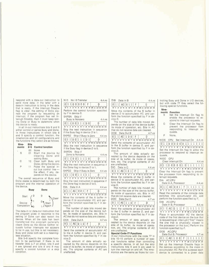
respond wrth a data-out rnstructlon to send more data, In the latter w ~ t h a data-~n ~nstructron to brmg In the data that IS ready. If the lnterrupt D~sabie flag IS clear, the sett~ng of Done s ~ g - nais the program by request~ng an Interrupt; rf the program has set In-terrupt Drsable, then rt must keep test- Ing Done or Busy to determ~ne when the dev~ce IS ready
In all rn-out ~nstruct~ons 8 and 9 b ~ t s erther control or sense Busy and Done in those mstructlons In whlch b ~ t s 8 and 9 spec~fy a control functron, the mnemonrcs and b ~ t conf~gurat~onsand the funct~ons they select are as follows
Mne- Bits rnonic 8-9 Control function
00 None S 01 Start the d e v ~ c e by
c lear ing Done and settlng Busy
C 10 Clear both Busy and Done, ~dlrng the deuce
P 11 Pulse the spec~al in- out bus control I ~ n e - the effect, rf any, de- pends on the dev~ce
The overall sequence of Busy and Done states is determined by both the program and the internal operat~on of the device.
Busy Done
Device Start Completion Again
The data-~n or data-out rnstructron that the program glves In response to the sett~ng of Done can also restart the dev~ce. When all the data has been transferred the program general ly clears Done so the dev~ce ne~ther re- quests further Interrupts nor appears to be In use, but t h ~ s IS not necessary Busy and Done both set IS a meanrng- less sltuatron.
B ~ t s 5-9 spec~fy the complete func- tlon to be performed. If there IS no transfer (brts 5-7 all alrke), bits 3 and 4 are Ignored and b ~ t s 8 and 9 may specify a control functron or a skrp condrtron.
N I 0 No I 0 Transfer 4.4 PS
Perform the control function specified by F in device D. SKPBN Skio if
Busy is onz zero 4.4 ss
1011 110 011 1 110 01 D 1 0'1 2 3 ' 4 5 6 ' 7 8 9'101112'131415
Skrp the next instruct~on In sequence rf the Busy flag In dev~ce D IS 1. SKPBZ S k ~ p~f Busy is Zero 4.4 ps
1011 110 011 1110 11 D 0'1 2 3 ' 4 5 6'7 8 9'10H12'131415
S k ~ p the next ~nstruction In sequence rf the Busy flag In devrce D IS 0. SKPDN Skrp if
Done IS Nonzero 4.4 PS
Skip the next rnstruction In sequence ~f the Done flag in device D is 1. SKPDZ ski^ ~f Busv is Zero 4.4 PS
Skrp the next instruct~on in sequence rf the Done flag rn devrce D is 0. DIA Data In A 4.4 zs
Move the contents of the A buffer In dev~ceD to accumulator AC, and per- form the functron spec~f~ed by F m de- vice D.
The number of data brts moved de- pends on the slze of the dev~ce buf- fer, its mode of operat~on, etc. B ~ t s In AC that do not receive data are cleared. DOA Data Out A 4.7 zs
Send the contents of accumulator AC to the A buffer in device D, and per- form the funct~on speclf~ed by F In de- vice D.
The amount of data actually ac-cepted by the dev~ce depends on the size of ~ t s buffer, its mode of operatlon, etc. The original contents of AC are unaffected.
DIB Data in B 4.4 zs
Move the contents of the B buffer in device D to accumulator AC, and per- form the funct~on specified by F in de- vice D.
The number of data bits moved de- pends on the slze of the device buffer, its mode of operation, etc. Bits in AC that do not receive data are cleared. DOE Data Out B 4.7 PS
1011 11 A C ) ~o 0 1 F I D 0 ' 1 2 3 ' 4 5 6 ' 7 8 9'101112'1314 15
Send the contents of accumulator AC to the B buffer in device D, and per- form the funct~on specifred by F m de- vice D.
The amount of data actually ac-cepted by the device depends on the size of ~ t s buffer, ~ t s mode of opera- tion, etc. The original contents of AC are unaffected DIC Data in C 4.4 PS
Move the contents of the C buffer In device D to accumulator AC, and per- form the function specified by F m de- vice 0.
The number of data brts moved de- pends on the size of the device buffer, ~ t s mode of operatlon, etc Bits in AC that do not receive data are cleared. DOC Data Out C 4.7 PS
(o (1 11 A C ( I 101 F I D 0'1 2 3'4 5 6 ' 7 8 9'101112'1314 15
Send the contents of accumulator AC to the C buffer in device D, and per- form the function specified by F In de- vice D.
The amount of data actually ac-cepted by the device depends on the size of its buffer, its mode of opera- tion, etc. The origmal contents of AC are unaffected. Special Code-77 Functions In-out instructions with the code 77 in bits 10-15 perform a number of spe- c ~ a l functions rather than controlling a specific dev~ce. In all but the skip mstruct~ons b ~ t s 8 and 9 are used to turn the interrupt on and off. The mne- rnonlcs are the same as those for con-
trolling Busy and Done In 1/0 devrces,' but wrth code 77 they select the f
lowrng spec~al functions. Mne-
monic Functlon S Set the Interrupt On flag to
enable the processor to re-spond to rnterrupt requests.
C Clear the lnterrupt On fiag to prevent the processor from respondrng to Interrupt re-quests
P None.
NlOS CPU Set lnterrupt On 4.4 PS
[0)1 110 010 0 010 111 1 1 1 1 1) 0 ' 1 2 3 ' 4 5 6 ' 7 8 9'101112'13 14 15
Set the lnterrupt On flag to allow the processor to respond to Interrupt re-quests. NlOC CPU
Clear Interrupt On 4.4 PS
011 110 010 0 011 011 1 1 1 1 1 0 ' 1 2 3 ' 4 5 6 7 8 9 '10 11 12'13 14 15
Zlear the lnterrupt On flag to prevent !he processor from respondmg to in-terrupt requests. DIA AC,CPU
Data In A, Processor 4.4 as
Read the contents of the console data switches rnto accurnulator AC, a r " perform the function specified by F.. DIB AC.CPU I
Data ln B, Processor 4.4 PS 1
011 1 1 ~ ~ 1 0 111 F 1 1 1 1 1 1 I 0 '1 2 3 ' 4 5 6 ' 7 8 9 '10 11 12'13 14 15
Place rn accumulator AC the device code of the frrst device on the bus that is request~ng an interrupt ("first" means the one that is physically closest to the processor on the bus.) Perform the function specified by F. DOB AC,CPU
Data Out B, Processor 4.7 zs
Set up the lnterrupt Disable flags in he devices accordmg to the mask in sccumulator AC. For this purpose each jevlce is connected to a given data

NOVA Options flag IS set or cleared as
Ing b ~ t In the mask IS
the function specified
Processor
I I . 1 L I C 1 1 1 1 1
5 6 ' 7 8 9 '10 11 12'13 14 15
~ n t r o l fiipflops, includmg and lnterrupt Disable, in
;es connected to the bus Per-&function specified by F. bCPU lu t C. Processor 4.7 as
the function specrfied by F. 1 halt the processor
CPU Skip ~f is Nonzero, Processor 4.4 as
? next ~nstruction in sequence brrupt On flag is 1.
CPU Skip if is Zero, Processor 4.4 as
s next instruction in sequence ~ p tOn is 0.
1K Read-only Memory Module (1024 words of 16 bits each) lncludes 1 K words (2K bytes) of Read- Only Memory whrch is mterchangeable w~th the alterable core memory w~th no wlrlng modifications required. The contents of t h~s module can be e~ther standard programs or spec~al cus- tomer spec~fred programs.
NOVA Central Processor -Rack Mountable lncludes central processor, console (with lock), high-speed data channel, power supply, five subassembly slots available in basic frame. This basic frame is rack mountable In a stan-dard 19" rack with slides.
NOVA Central Processor -Table Top Model lncludes central processor, console (w~th lock), high-speed data channel power supply, f~ve subassembly slots available in basic frame. This basic frame is enclosed in a cabinet de-signed for table top use.
4K Core Memory (4096 words of 16-bits each) lncludes 4K words (8K bytes) of mern- ory with al l necessary electronrcs mounted on a single subassembly (15Nx151r printed circu~t card) which
Expanslon Enclosure This item is a basic frame with a power supply and slots to mount seven (7) subassemblies. This unrt IS typr-cally mounted directly above the cen- tral processor frame and 1s used to mount add~tronal memory (alterable core or Read Only), addit~onal I f 0 controllers, or spec~al customer de-s~gned hardware.
Power Monitor and Auto Restart Prov~des power level detection and a flag which is attached to the Program lnterrupt and can be sensed by the program Its function IS to allow the program to become aware of an im-minent power fa~iure so rt can prov~de for an orderly shut down. The program automat~cally restarts at location 0.
Real-Time Clock Thrs opt~on provides a flag whrch can be enabled by the program to prov~de a program ~nterrupt at a fixed frequency. E~ther the AC lme or a crystal clock may be specrf~ed as the trme source
Teletype InputIOutput Interface This option prov~des an interface to any one of the Teletype models listed below: Teletype ASR33 Keyboardfprlnter, 8 channel reader1 punch, 10 char./sec. Teletype KSR33 Keyboardlprinter, 10 char./sec. Teletype KSR35 Keyboardfprlnter, 10 char./sec. Teletype KSR37 Keyboardlprinter (upperllower case), 15 char./sec.
High-speed Perforated Tape Reader and Control Paper tape reader and control which senses erght channel, fan fold perfo- rated Mylar or paper tape photo- electr~cally at 150 or 300 characters
High-speed Perforated Tape Punch and Control BRPEII Punch and Control which punches eight channel fan fold paper tape at 63.3 characters per second.
Cathode Ray Tube Display and Control This equipment includes a Tektron~x Type 602 5" Rectangular Display and a control interface operating in a point plotting mode (256 points x 256 points) using the Data Channel for display refresh.
Medium-Speed Line Printer and Control Th~s option includes a Potter Medium- Speed L~ne Printer Type HSP3502 and control This IS a chain prmter w~th a full ASCII interface mcluding paper advance (LF, FF) characters.
Card Reader and Control Soroban SCCR card reader and control whch operates at 225, 400 or 600 cards per mmute.
Incremental Plotter Plotters and control mterfaces to un~ts made by two d~fferent manufacturers. 1) The Cal~forn~a Computer Products 500 Ser~es un~ts (Drum or Flat Bed Style). 2) The Houston Instruments Complot DP-I Drg~tal Plotter which uses '7 fold" style paper.
In addition, the foliowmg devices will be available magnetic disk, Incremen- tal tape, IBM compatible magnetlc tape, and a com'plete line of AID and DIA equipment.
sembler recognizes a number I can be plugged directly into one of the slots in the basic frame with no wiring modifications required.
Octal I 2K Core Memory
: tn%errupt NlOC CPU 060277gitQeDIB -,CPL! 06,477
(2049 words of 16 bits each) lncludes 2K words (4K bytes) of mem- ory mounted on a smgie subassembly (15Mx15ff printed circuit card) which can be plugged directly into one of the slots in the bas~c frame with no wiring modifications required.
1K Core Memory (1024 words of 16 bits each) lncludes 1 K words (2K bytes) of mem- ory mounted on a smgle subassembly (15f'x15u printed circuit card) which can be plugged directly rnto one of the slots in the basic frame with no wiring


