ee109 digital logic practice problem...
TRANSCRIPT

1
2 Practice Problem Solutions The following are solutions to the set of practice problems presented
separately Use these only after attempting the problems on your own
2
HW2 - Number Systems and Conversions
1
a 11101100101112
= 126 + 125 +124 + 122 + 121 + 12-2 + 12-4 + 12-5 + 12-6
= 118359375 10
= 001 | 110 | 110010 | 1112 = 166278
= 0111 | 01100101 | 11002 = 765C16
b 15B3516
= 1162 + 5161 +11160 + 316-1 + 516-2 = 3472070312510
= 0001 | 0101 | 10110011 | 01012
= 101 | 011 | 011001 | 101 | 0102 = 5331528
2 Use the Making Change method
a Start by listing the powers of 2 and then find the coefficients of the
number by starting with the largest powers and working toward lower
powers determining which ones sum to the desired value
0 1 1 1 0 0 1 1 0 1 1 1 0 1
1024 512 256 128 64 32 16 8 4 2 1 5 25 125
(923625)10 = (1110011011101)2
3
a 45301528
= 100 101 011 000001 101 012
= 1001 | 0101 | 10000011 | 01012 = 9583516
4
a DABBAD0016
= 1101 1010 1011 10111010 11012
= 001 | 101 | 101 | 010 | 111 | 011101 | 011 | 0102 = 1552735328
b BADA16 = 11162 + 10161 +13160 + 1016-1 = 298962510
5 Use the Making Change method Start by listing the powers of 5 and then find
the coefficients of the number by starting with the largest powers and working
toward lower powers determining which ones sum to the desired value
a
0 3 2 0 3 3 3 1
3125 625 125 25 5 1 2 04
(214364)10 = (3203331)5
3
HW3 - Boolean Algebra Logic Functions and Canonical
Representation 2-Level Implementations
1 Probably the easiest method is perfect induction (ie a truth table)
F = X + Xrsquo = 1
X Xrsquo F
0 1 1
1 0 1
2
a
F = WXYZ bull (WXYZ + WXYZ + WXYZ +WXYZ)
= WWXXYYZZrsquo bull WWXXrsquoYYZZ + WrsquoWXXYYZZ +
WWXXYYrsquoZZ T8
= WXYZZrsquo + WXXrsquoYZ + WWrsquoXYZ + WXYYrsquoZ T3rsquo
= 0 + 0 + 0 + 0 + 0 T5rsquo
= 0 A4rsquo
b
F = AB + ABCrsquoD + ABDErsquo + ABCrsquoE + CrsquoD
= AB bull (1 + CrsquoD + DErsquo + CrsquoE) + CrsquoD T8
= AB bull (1 + DErsquo + CrsquoE) + CrsquoD T6
= AB bull (1) + CrsquoD T2
= AB + CrsquoD T1rsquo
3
a F = XY + XYZrsquo
XYZ Xrsquo Xrsquo bull Y Yrsquo Zrsquo Xrsquobull Yrsquo bull Zrsquo F
000 1 0 1 1 1 1
001 1 0 1 0 0 0
010 1 1 0 1 0 1
011 1 1 0 0 0 1
100 0 0 1 1 0 0
101 0 0 1 0 0 0
110 0 0 0 1 0 0
111 0 0 0 0 0 0
4
b F = Wrsquo + X bull (Y + Z)
WXYZ Wrsquo Yrsquo Yrsquo+Z Xrsquo Xrsquo bull (Yrsquo+Z) F
0000 1 1 1 1 1 1
0001 1 1 1 1 1 1
0010 1 0 0 1 0 1
0011 1 0 1 1 1 1
0100 1 1 1 0 0 1
0101 1 1 1 0 0 1
0110 1 0 0 0 0 1
0111 1 0 1 0 0 1
1000 0 1 1 1 1 1
1001 0 1 1 1 1 1
1010 0 0 0 1 0 0
1011 0 0 1 1 1 1
1100 0 1 1 0 0 0
1101 0 1 1 0 0 0
1110 0 0 0 0 0 0
1111 0 0 1 0 0 0
c F = (A + B + CD) bull (B + C + D)
ABCD Arsquo Brsquo CD A + B + CD Crsquo Drsquo B + C + Drsquo F
0000 1 1 0 1 1 1 1 1
0001 1 1 0 1 1 0 1 1
0010 1 1 0 1 0 1 1 1
0011 1 1 1 1 0 0 0 0
0100 1 0 0 1 1 1 1 1
0101 1 0 0 1 1 0 1 1
0110 1 0 0 1 0 1 1 1
0111 1 0 1 1 0 0 1 1
1000 0 1 0 1 1 1 1 1
1001 0 1 0 1 1 0 1 1
1010 0 1 0 1 0 1 1 1
1011 0 1 1 1 0 0 0 0
1100 0 0 0 0 1 1 1 0
1101 0 0 0 0 1 0 1 0
1110 0 0 0 0 0 1 1 0
1111 0 0 1 1 0 0 1 1
5
d
F = (((Arsquo + B) + C ) + D)
= ((Arsquo + B)rsquo + C) bull Drsquo DEMORGANS
= (A bull Brsquo + Crsquo) bull Drsquo DEMORGANS
= ABrsquoDrsquo + CrsquoDrsquo T8
ABCD Brsquo Drsquo AbullBrsquobullDrsquo Crsquo CrsquobullDrsquo F
0000 1 1 0 1 1 1
0001 1 0 0 1 0 0
0010 1 1 0 0 0 0
0011 1 0 0 0 0 0
0100 0 1 0 1 1 1
0101 0 0 0 1 0 0
0110 0 1 0 0 0 0
0111 0 0 0 0 0 0
1000 1 1 1 1 1 1
1001 1 0 0 1 0 0
1010 1 1 1 0 0 1
1011 1 0 0 0 0 0
1100 0 1 0 1 1 1
1101 0 0 0 1 0 0
1110 0 1 0 0 0 0
1111 0 0 0 0 0 0
4
a
F = XYZ (023)
= m0 + m2 + m3
= XrsquoYrsquoZrsquo + XrsquoYZrsquo + XrsquoYZ
= XYZ (14567)
= M1 bull M4 bull M5 bull M6 bull M7
= (X+Y+Zrsquo)bull(Xrsquo+Y+Z)bull(Xrsquo+Y+Zrsquo)bull(Xrsquo+Yrsquo+Z)bull(Xrsquo+Yrsquo+Zrsquo)
b
F = ABC (1246)
= M1 bull M2 bull M4 bull M6
= (A + B + Crsquo) bull (A + Brsquo + C) bull (Arsquo + B + C) bull (Arsquo + Brsquo + C)
= ABC (0357)
= m0 + m3 + m5 + m7
= ArsquoBrsquoCrsquo + ArsquoBC + ABrsquoC + ABC
6
c
F = ABCD(1257)
= m1 + m2 + m5 + m7
= ArsquoBrsquoCrsquoD + ArsquoBrsquoCDrsquo + ArsquoBCrsquoD +ArsquoBCD
= ABCD (034689101112131415)
= M0 bull M3 bull M4 bull M6 bull M8 bull M8bull M9 bull M10 bull M11 bull M12 bull M13 bull
M14 bull M15
= (A + B + C +D) bull (A + B + Crsquo +Drsquo) bull (A + Brsquo + C +D)
bull (A + Brsquo + Crsquo +D) bull (Arsquo + B + C +D) bull (Arsquo + B + C +Drsquo)
bull (Arsquo + B + Crsquo +D) bull (Arsquo + B + Crsquo +Drsquo) bull (Arsquo + Brsquo + C +D)
bull (Arsquo + Brsquo + C +Drsquo) bull (Arsquo + Brsquo + Crsquo +D) bull (Arsquo + Brsquo + Crsquo +Drsquo)
d
F = X + YZ +YZ = Xrsquo + YZrsquo T3
= Xrsquo(Y + Yrsquo)(Z + Zrsquo) + (X+Xrsquo)(YZrsquo) T1rsquoT5
= XrsquoYrsquoZrsquo + XrsquoYrsquoZ + XrsquoYZrsquo + XrsquoYZ + XYZrsquo + XrsquoYZrsquo T8
= m0 + m1 + m2 + m3 + m6
= XYZ(01236)
= XYZ(457)
= M4 bull M5 bull M7
= (Xrsquo + Y + Z) bull (Xrsquo + Y + Zrsquo) bull (Xrsquo + Yrsquo + Zrsquo)
e
F = AB +BC +ACrsquo
= (ArsquoBC + ArsquoBCrsquo) + (ABrsquoC + ArsquoBrsquoC) + (ABCrsquo + ABrsquoCrsquo) T10
= m3 + m2 + m5 + m1 + m6 + m4
= ABC (123456)
= ABC(07)
= M0 bull M7
= (A + B + C) bull (Arsquo + Brsquo + Crsquo)
5
X + Y X + Yrsquo X
= bull x y x y x y
7
6 One possible solution
XY + XrsquoZ + YZ
XY + XrsquoZ + YZ bull 1 T1rsquo
XY + XrsquoZ + YZ bull (X + Xrsquo) T5
XY + XrsquoZ + XYZ + XYZ T8
(XY + XYZ) + (XrsquoZ + XrsquoZY) T6
XY + XrsquoZ T9
7
a
F = XrsquoZrsquo + (Y(Xrsquo+Z))rsquo
= XrsquoZrsquo + Yrsquo + (Xrsquo+Z)rsquo DEMORGANS
= XrsquoZrsquo + Yrsquo + XZrsquo DEMORGANS
= (Xrsquo + X) bull Zrsquo + Yrsquo T8
= 1 bull Zrsquo + Yrsquo T5
POS = Zrsquo + Yrsquo T1rsquo
b
G = XY + YrsquoZrsquo
= (XY + Yrsquo)(XY + Zrsquo) T8rsquo
= (X + Yrsquo)(Y + Yrsquo)(X + Zrsquo)(Y + Zrsquo) T8rsquo
= (X + Yrsquo)(X + Zrsquo)(Y + Zrsquo) T3rsquo
= (X + Yrsquo)(Y + Zrsquo) T11rsquo
POS = (X + Yrsquo) bull (Y + Zrsquo)
c
H = AB bull (CD)rsquo + A + D
= (AB bull (Crsquo + Drsquo)) + A + D DEMORGANS
= (AB + A + D) bull (Crsquo + Drsquo + A + D) T8rsquo
= (A(B+1) + D) bull (1)
= (A + D) bull 1 T1rsquo
POS = A + D
8
Z = AB + (Crsquo + ArsquoBrsquo)rsquo + Arsquo(AB + ACrsquoDrsquo)
= AB + (Crsquo + ArsquoBrsquo)rsquo + ArsquoAB + ArsquoACrsquoDrsquo T8
= AB + Cbull (A+B) + 0 + 0 DEMORGANS T5rsquo
SOP = AB + AC + BC T8
9
a F = xrsquoyrsquo + xyrsquoz + zrsquo
Let us simplify first
= yrsquo(xrsquo + xz) + zrsquo
= yrsquo(xrsquo(z + zrsquo) + xz) + zrsquo T1rsquo T5
= yrsquo(xrsquoz + xrsquozrsquo + xz) + zrsquo T8
8
= yrsquo(xrsquoz + xrsquoz + xrsquozrsquo + xz) + zrsquo T3 (replicate terms)
= yrsquo(xrsquo(z+zrsquo) + z(xrsquo+x)) + zrsquo T8
= yrsquo(xrsquo +z) + zrsquo T5T1rsquo
Now let us convert to POS using T8rsquo
= (zrsquo+yrsquo)(zrsquo + xrsquo + z) T8rsquo
= (zrsquo+yrsquo) T5T1rsquo
b G = (xrsquo+yrsquo)(y)(wrsquo+y+z)
Convert to SOP using T8 (simplifying as we go)
= (xrsquoy + yrsquoy)(wrsquo + y + z) T8
= xrsquoy(wrsquo + y + z) T5rsquoT1
= wrsquoxrsquoy + xrsquoy + xrsquoyz T8
= xrsquoy(wrsquo + 1 + z) T8
= xrsquoy T2 T1rsquo
9
HW4 - Circuit Design w Karnaugh Maps
1
a F = ABCD(12459101213)
FSOP = CD BC BCD+ +
b F = MNOP(01289)
FSOP = N OP MO+ +
c F = ABCD (01258101115)
1
1
0
1 1
1 1 1 1
3
12 8
9 13 5 1
00 01 11 10
00
01
2 6
7 15
14 10
11
4
11
10
AB
CD
1
1
1
1
1 0
1
1 1
3
12 8
9 13 5 1
00 01 11 10
00
01
2 6
7 15
14 10
11
4
11
10
AB
CD
1
1
1
1
1
1
1
0
1 1
1 1
3
12 8
9 13 5 1
00 01 11 10
00
01
2 6
7 15
14 10
11
4
11
10
MN
OP
10
FSOP = ACD ACD BD+ +
d F = WXYZ (3671214)
FSOP = WY WZ X Z+ +
2
a F = XrsquoYrsquo + XrsquoZrsquo + WrsquoX + XYZ
FPOS = (Wrsquo + Xrsquo + Y)(X + Yrsquo + Zrsquo)(Wrsquo + Xrsquo + Z)
b The 4-bit prime numbers are 2 3 5 7 11 13
FPOS = (C+D)(Brsquo+D)(Arsquo+D)(Arsquo+B+C)
1
1
1
1
1 0
1 1
1 1 1 1
3
12 8
9 13 5 1
00 01 11 10
00
01
2 6
7 15
14 10
11
4
11
10
WX
YZ
0
1
1
1
1
0
0
1
1 0
1 0 1
1 0 1 1
3
12 8
9 13 5 1
00 01 11 10
00
01
2 6
7 15
14 10
11
4
11
10
WX
YZ
1
1
1
0
0
1
0
0 0
0 0 0
0 1 1 0
3
12 8
9 13 5 1
00 01 11 10
00
01
2 6
7 15
14 10
11
4
11
10
AB
CD
11
c The 4-bit numbers that are not perfect squares or cubes are 2 3 5 6 7
10 11 12 13 14 15
FPOS = (B + C)(A + C + D)
d The 4-bit numbers divisible by 3 or 5 are 0 3 5 6 9 10 12 15
FPOS = (A+B+C+Drsquo)(A+B+Crsquo+D)(A+Brsquo+C+D)(A+Brsquo+Crsquo+Drsquo)(Arsquo+B+C+D)bull
(Arsquo+B+Crsquo+Drsquo)(Arsquo+Brsquo+C+Drsquo)(Arsquo+Brsquo+Crsquo+D)
3 The K-Maps are below
FSOP = CD BC BCD+ +
1
1
1
1
1
1
1
1
0 0
0 1 0
0 1 1 0
3
12 8
9 13 5 1
00 01 11 10
00
01
2 6
7 15
14 10
11
4
11
10
AB
CD
1
0
0
1
1
0
0
1
1 0
0 1 0
1 0 1 0
3
12 8
9 13 5 1
00 01 11 10
00
01
2 6
7 15
14 10
11
4
11
10
AB
CD
1
1
0
1 1
1 1 1 1
3
12 8
9 13 5 1
00 01 11 10
00
01
2 6
7 15
14 10
11
4
11
10
AB
CD
12
FPOS = ( )( )( )C D B C B C D+ + + +
a AND ndash OR Implementation
B
Crsquo
D
CDrsquo
Brsquo
b OR - AND Implementation
Drsquo
Crsquo
Brsquo
CD
B
0
0
0
0
0
0
0 0
0
3
12 8
9 13 5 1
00 01 11 10
00
01
2 6
7 15
14 10
11
4
11
10
AB
CD
13
c NAND - NAND Implementation
B
Crsquo
D
CDrsquo
Brsquo
d NOR - NOR Implementation
Drsquo
Crsquo
Brsquo
CD
B
14
4
a The values with an odd number of 1s are 1 2 4 7 8 11 13 14 The
Donrsquot Care numbers are 0 4 5 8 10 12 and 15
SOP = ArsquoCrsquo + BD + AC + BrsquoDrsquo
b F = BrsquoCrsquoDrsquo + BCDrsquo + ABCrsquoD d = ArsquoBCrsquoD + ArsquoBrsquoCDrsquo
F = (A+Arsquo)BrsquoCrsquoDrsquo + (A+Arsquo)BCDrsquo + ABCrsquoD
= ABrsquoCrsquoDrsquo + ArsquoBrsquoCrsquoDrsquo + ABCDrsquo + ArsquoBCDrsquo + ABCrsquoD
d = ArsquoBCrsquoD + ArsquoBrsquoCDrsquo
FSOP = BrsquoCrsquoDrsquo + BCrsquoD + BCDrsquo
1
1
d
1
1
d
d 0
1 d 1
1 d 1
3
12 8
9 13 5 1
00 01 11 10
00
01
2 6
7 15
14 10
11
4
11
10
AB
CD
d
1
1
1 0
1
1 d
3
12 8
9 13 5 1
00 01 11 10
00
01
2 6
7 15
14 10
11
4
11
10
AB
CD
15
5
a F = ArsquoC + ACE + CABrsquo + BrsquoArsquoDE + Arsquo Drsquo Ersquo
FSOP = ArsquoC + ArsquoDrsquoErsquo + ArsquoBrsquoDE + BrsquoC + CE
b F = (AB + ArsquoBrsquo) (CrsquoDrsquo + CD)
= ABCrsquoDrsquo + ArsquoBrsquoCrsquoDrsquo + ABCD + ArsquoBrsquoCD
bull K-Map
FSOP = ABCrsquoDrsquo + ArsquoBrsquoCrsquoDrsquo + ABCD + ArsquoBrsquoCD
1
1
1 0
1
3
12 8
9 13 5 1
00 01 11 10
00
01
2 6
7 15
14 10
11
4
11
10
AB
CD
1
0
1
1
1
1
0
0
1 0
1 1 1
0 1 1
3
12 8
9 13 5 1
00 01 11 10
00
01
2 6
7 15
14 10
11
4
11
10
BC
DE
0
0
1
1
1
0
0
0
0 0
1 0 0
0 1 1 0
3
12 8
9 13 5 1
00 01 11 10
00
01
2 6
7 15
14 10
11
4
11
10
BC
DE
A=0 A=1
16
bull NAND ndash NAND Implementation
B
Crsquo
Drsquo
D
C
A
Arsquo
Brsquo
c F = ArsquoBrsquoCrsquoDrsquo + ArsquoBrsquoCDrsquo + ArsquoBCrsquoDrsquo + ArsquoBCrsquoD + ABrsquoCDrsquo
bull K-Map
FSOP = ArsquoCrsquoDrsquo + ArsquoBCrsquo + BrsquoCDrsquo
bull NAND ndash NAND Implementation
ArsquoCrsquo
Drsquo
B
Brsquo
C
1
1
1 0
1
1
3
12 8
9 13 5 1
00 01 11 10
00
01
2 6
7 15
14 10
11
4
11
10
AB
CD
F
F
17
d The numbers are 2 3 4 5 10 12 13 14 15
bull K-Map
SOP = AB + BCrsquo + ArsquoBrsquoC + ACDrsquo
bull NAND ndash NAND Implementation
A
B
Crsquo
ArsquoBrsquoC
Drsquo
1
1
1
1
1
0
1 1
1 1
3
12 8
9 13 5 1
00 01 11 10
00
01
2 6
7 15
14 10
11
4
11
10
AB
CD
18
6
a F = ArsquoC + ACE + CABrsquo + BrsquoArsquoDE + Arsquo Drsquo Ersquo
bull K-Map
FPOS = (Arsquo + Crsquo)(Arsquo + Brsquo + E)(Brsquo+C+Ersquo)(C + D + Ersquo)(C + Drsquo + E)
b F = (AB + ArsquoBrsquo) (CrsquoDrsquo + CD)
bull K-Map
FPOS = (A + Brsquo)(Arsquo + B)(C + Drsquo)(Crsquo + D)
0
0
0
0
0
0
0
0 0
0 0 0 0
3
12 8
9 13 5 1
00 01 11 10
00
01
2 6
7 15
14 10
11
4
11
10
AB
CD
1
0
1
1
1
1
0
0
1 0
1 1 1
0 1 1 0
3
12 8
9 13 5 1
00 01 11 10
00
01
2 6
7 15
14 10
11
4
11
10
BC
DE
0
0
1
1
1
0
0
0
0 0
1 0 0
0 1 1 0
3
12 8
9 13 5 1
00 01 11 10
00
01
2 6
7 15
14 10
11
4
11
10
BC
DE
A=0 A=1
19
NOR ndash NOR Implementation
A
Brsquo
Arsquo
B
CDrsquo
Crsquo
D
c F = ArsquoBrsquoCrsquoDrsquo + ArsquoBrsquoCDrsquo + ArsquoBCrsquoDrsquo + ArsquoBCrsquoD + ABrsquoCDrsquo
bull K-Map
FPOS = (B + Drsquo)(Brsquo + Crsquo)(Arsquo + C)
bull NOR ndash NOR Implementation
B
Drsquo
BrsquoCrsquo
ArsquoC
0
0
0
0
0
0
0
0 0
0 0 0
3
12 8
9 13 5 1
00 01 11 10
00
01
2 6
7 15
14 10
11
4
11
10
AB
CD
F
F
20
d The numbers are 2 3 4 5 10 12 13 14 15
bull K-Map
POS = (B + C)(A + Brsquo + Crsquo)(Arsquo + B + Drsquo)
bull NOR ndash NOR Implementation
BC
ABrsquoCrsquo
Arsquo
Drsquo
7 A and B are both 2-bit signed numbers They range from -2 to +1 Thus F = A + B
is ranging from -4 to +2 We need 3 bits to represent the signed number F
a The block diagram is below
A1
A0
B1
B0
F2
F1
F0
0
0
0
0 0
0
0 0
3
12 8
9 13 5 1
00 01 11 10
00
01
2 6
7 15
14 10
11
4
11
10
AB
CD
F
21
b The truth table is below
A1 A0 B1 B0 F2 F1 F0
0 0 0 0 0 0 0
0 0 0 1 0 0 1
0 0 1 0 1 1 0
0 0 1 1 1 1 1
0 1 0 0 0 0 1
0 1 0 1 0 1 0
0 1 1 0 1 1 1
0 1 1 1 0 0 0
1 0 0 0 1 1 0
1 0 0 1 1 1 1
1 0 1 0 1 0 0
1 0 1 1 1 0 1
1 1 0 0 1 1 1
1 1 0 1 0 0 0
1 1 1 0 1 0 1
1 1 1 1 1 1 0
c
K-Map of output ldquoF2rdquo K-Map of output ldquoF1rdquo
F2SOP = A1A0rsquo + B1B0rsquo + A1B1 + A1B0rsquo + A0rsquoB1
F1SOP = A1B1rsquoB0rsquo + A1A0rsquoB1rsquo + A1rsquoA0rsquoB1 + A1rsquoB1B0rsquo + A1rsquoA0B1rsquoB0 + A1A0B1B0
1
1
1
1
1
1
1
0
1 1
1
3
12 8
9 13 5 1
00 01 11 10
00
01
2 6
7 15
14 10
11
4
11
10
A1A0
B1B0
1
1
1
1
0
1 1
1 1
3
12 8
9 13 5 1
00 01 11 10
00
01
2 6
7 15
14 10
11
4
11
10
A1A0
B1B0
22
K-Map of output ldquoF0rdquo
F0SOP = A0B0rsquo + A0rsquoB0
d AND-OR implementation
Implementation of F2
A1A0
B1
B0
Implementation of F1
The implementation consists of four 3-input AND gates two 4-input AND gates and one
6-input OR gate
Implementation of F0
A0B0
A0
B0
1
1
1
1
0
1 1
1 1
3
12 8
9 13 5 1
00 01 11 10
00
01
2 6
7 15
14 10
11
4
11
10
A1A0
B1B0
23
NAND ndash NAND Implementation
(1) Implementation of F2
A1A0
B1
B0
(2) Implementation of F1
The implementation consists of four 3-input NAND gates two 4-input NAND gates and
one 6-input NAND gate
(3) Implementation of F0
A0B0
A0
B0
24
8 X is a 3-bit unsigned number It ranges from 0 to 7 Thus Y = 3X + 1 is ranging
from 1 to 22 We need 5 bits to represent the unsigned number Y
a The block diagram is below
X2
X1
X0
Y4
Y3Y2
Y1
Y0
b The truth table is below
X X2 X1 X0 Y4 Y3 Y2 Y1 Y0 Y
0 0 0 0 0 0 0 0 1 1
1 0 0 1 0 0 1 0 0 4
2 0 1 0 0 0 1 1 1 7
3 0 1 1 0 1 0 1 0 10
4 1 0 0 0 1 1 0 1 13
5 1 0 1 1 0 0 0 0 16
6 1 1 0 1 0 0 1 1 19
7 1 1 1 1 0 1 1 0 22
c
K-Map of output ldquoY4rdquo K-Map of output ldquoY3rdquo
Y4POS = X2(X1 + X0) Y3POS = (X2 + X1)(X1rsquo + X0)(X2rsquo + X0rsquo)
K-Map of output ldquoY2rdquo
Y2POS = (X2 + X1 + X0)( X2 + X1rsquo + X0rsquo)( X2rsquo + X1rsquo + X0)( X2rsquo + X1 + X0rsquo)
0 0
0 0
0 0
6 4
5 7 3 1
00 01 11 10
0
1
2
X2X1
X0
0 0
0 0
0 0 0
6 4
5 7 3 1
00 01 11 10
0
1
2
X2X1
X0
0 0
0
0 0
6 4
5 7 3 1
00 01 11 10
0
1
2
X2X1
X0
25
K-Map of output ldquoY1rdquo K-Map of output ldquoY0rdquo
Y1POS = X1 Y0POS = X0rsquo
d
bull OR ndash AND Implementation
Implementation of Y4
X1
X0
X2
Implementation of Y3
X2
X1
X1
X0
X2
X0
0 0
0
0 0
6 4
5 7 3 1
00 01 11 10
0
1
2
X2X1
X0
0
0 0 0 0
6 4
5 7 3 1
00 01 11 10
0
1
2
X2X1
X0
26
Implementation of Y2
X2X1X0
X1
X0
X2
Implementation of Y1 (straight wire connection)
Y1X1
Implementation of Y0 (straight wire connection)
Y0X0
bull NOR ndash NOR Implementation
Convert all gates in the above implementations to NOR gates For Y1 and Y0 just use
wires
27
e This will not be covered at this point of the class since we have not yet discussed
adders Ignore this question
9 X is a 3-bit signed number It ranges from -4 to +3
Thus Z = X2 + 2X + 1 = (X + 1)2 is ranging from 0 to +16 We need 6 bits to
represent signed number Z
a The block diagram is below
Z5
Z4
Z3
Z2Z1
Z0
X0
X1
X2
b The truth table is below
X X2 X1 X0 Z5 Z4 Z3 Z2 Z1 Z0 Z
+0 0 0 0 0 0 0 0 0 1 +1
+1 0 0 1 0 0 0 1 0 0 +4
+2 0 1 0 0 0 1 0 0 1 +9
+3 0 1 1 0 1 0 0 0 0 +16
-1 1 1 1 0 0 0 0 0 0 +0
-2 1 1 0 0 0 0 0 0 0 +1
-3 1 0 1 0 0 0 0 0 0 +4
-4 1 0 0 0 0 1 0 0 1 +9
c
No K-Map needed for Z5 ldquoZ5rdquo = 0
K-Map of output ldquoZ4rdquo K-Map of output ldquoZ3rdquo
Z4SOP = X2rsquoX1X0 Z3SOP = X2rsquoX1X0rsquo + X2X1rsquoX0rsquo
0
1
6 4
5 7 3 1
00 01 11 10
0
1
2
X2X1
X0
0
1 1
6 4
5 7 3 1
00 01 11 10
0
1
2
X2X1
X0
28
K-Map of output ldquoZ2rdquo K-Map of output ldquoZ0rdquo
Z2SOP = X2rsquoX1rsquoX0 Z0SOP = X2rsquoX0rsquo + X1rsquoX0rsquo
Note Z1 = 0 (constant)
0
1
6 4
5 7 3 1
00 01 11 10
0
1
2
X2X1
X0
1 0
1 1
6 4
5 7 3 1
00 01 11 10
0
1
2
X2X1
X0
29
10 Design a 1-bit comparator that takes in a bit X and a bit Y and outputs XltY
XgtY X=Y Use a single 2-to-4 decoder and 1 single OR gate
Consider the truth table of each of these simple functions We can implement
each as a sum of minterms And since a decoder implements the minterms of
the input variables we can arrive at the circuit above
X Y XltY XgtY X==Y
0 0 0 0 1
0 1 1 0 0
1 0 0 1 0
1 1 0 0 1
Y0
Y1
Y2
Y3
A0
A1
2-t
o-4
Decoder
X
Y XltY
XgtY
X=Y
30
HW5 - Signed Representations and Arithmetic
1
a
11 1
10100 = 20
+ 11101 = 29
Carry=1 110001 = 49
b
11100
- 10100
01000
28
- 20
8
1 1 1 1 _
11100
2rsquos comp 01011
+ 1
01000
2
b
1 1 1 1 _
101011
+ 011010
1000101
3 For unsigned subtraction we still use take the 2s complement of the bottom
number (but the check for overflow differs for unsigned vs 2s complement)
a 01101102 ndash 01001002 cannot be performed as is because we cannot
subtract a larger number from a smaller number in unsigned
representation
0110110
- 0100100
+54
-60
-6
1 1 1 1 1 1 _
0110110
2rsquos comp 1011011
+ 1
0010010
4
a Unsigned binary 28 lt 28310 lt 29 Therefore 9 bits 28310 = 1000110112
b 2rsquos complement with n-bits we can make ndash(2n-1) to +(2n-1-1) With n = 9
the range is -256 to +256 With n = 10 the range is -512 to +511 Thus
10 bits 28310 = 1000110112
5 Consider the following decimal numbers +21 +55 +121 -32 -99 -128
a What are the corresponding 8-bit signed-magnitude representation
31
a What are the corresponding 8-bit 2s complement representation
b Which of the above numbers can be represented in 6-bit signed-
magnitude 6-bit 1s complement 6-bit 2s complement representations
explain
21 55 121 -32 -99 -128 A 16+4+1=21
00010101 00110111 01111001 10100000 11100011 NA
B 00010101 00110111 01111001 1110000 10011101 10000000 C YYY
010101 in all cases
NNN NNN NNY 100000 in 2rsquos comp
NNN NNN
6 What are the corresponding decimal representations for the following binary
numbers 01011011 11010010 if
a The binary numbers are in 8-bit signed-magnitude format
b The binary numbers are in 8-bit 2s complement format
01011011 11010010 a) 64+16+8+2+1=91 -(64+16+2)=-82 b) 64+16+8+2+1=91 -128+64+16+2=-46
7 Perform the following addition problems for the following 2rsquos complement
numbers State whether overflow does or does not occur for each problem
Justify your answer for why overflow does or does not occur Check your
work by converting each number to decimal
a 1010 0111 b 1001 0110 c 0101 1100 d 0101 1101
+1110 0100 +1011 0011 +1011 0101 +0110 1001
11000 1011 10100 1001 10001 0001 1100 0110
n+n=n
cin=cout=1
No Overflow
n+n=p
cin=0cout=1
Overflow
p+n=p
cin=cout=1
NoOverflow
p+p=n
cin=1cout=0
Overflow
8 This is an exercise to help you remember what gates are used to create a full
adder Using a full adder as shown below and no other gates can you
produce the function Z = AbullB (Hint Write out the logical equations for S
and Cout and see if you can hook up the inputs to produce Z)
ANSWER
Cin X Y S Cout
0 0 0 0 0
32
0 0 1 1 0
0 1 0 1 0
0 1 1 0 1
1 0 0 1 0
1 0 1 0 1
1 1 0 0 1
1 1 1 1 1
S X Y Cin
Cout XY XCin YCin
=
= + +
We want Z=XY and if we set Cin=0 then the formulas of S and Cout
becomes as follows
S X Y
Cout XY
=
=
Thus Cout = Z = XY
X Y
S
CinFull Adder
Cout
A B
0Z
33
9 Using 1 half-adder and a minimal number of 4-bit binary adders design a
circuit to calculate Y = 25X where X is a 4-bit inputs
ANSWER
If a number is multiplied by a number that is a power of 2 then the number rewritten
using the above formula
2 00
n
n X X=
Y = 25X = 16X + 8X + X = X0000+X000+X
Also adding the information that X is a 4-bit number above formula can be re-written
X = X3X2X1X0
Y = X3X2X1X00000 + X3X2X1X0000 + X3X2X1X0
This can be written as addition by 4 bit adders
X3 X2 X1 X0
X3 X2 X1 X0 0 0 0
+ X3 X2 X1 X0 0 0 0 0
Since one row in each addition is all zeros they can be eliminated and the other two
numbers can be added using a 4-bit adder However the lower bits require only a single
bit adder The carry from the first addition is transferred to the next one
B3 B2 B1 B0 A3 A2 A1 A0
S0S1S2S3
C0C4 4-bit Binary Adder
X Y
S
Half AdderCout
X3 X0X0X1X2X3 X1X2X30 X0X1X2
Y8 Y7 Y6 Y5 Y4 Y3 Y0Y1Y2
34
10 Using a minimal number of 4-bit adders design a circuit that implements
Y=20X+107 where X is a 3-bit unsigned number
ANSWER
X = X2X1X0 and thus 20X= 16X+4X These numbers are achieved by inserting zeros
at the end Once we add these there numbers we see that not all bits require addition We
actually need only a single 4-bit adder and nothing more
1 1 0 1 0 1 1
X2 X1 X0 0 0
+ X2 X1 X0 0 0 0 0
Which can be collapsed to the following addition
1 1 X2 X1 X0 0 0
+ X2 X1 X0 1 0 1 1
B3 B2 B1 B0 A3 A2 A1 A0
S0S1S2S3
C0C4 4-bit Binary Adder
X0X1X2 X1X211
11
X0
Y7 Y6 Y5 Y4 Y3 Y0Y1Y2
0
1
35
11 Design a minimal circuit using ANDORNOT gates to implement the
comparison A gt 10 where A is a 4-bit number
a Start by writing out the logical algorithm for when A gt 10 then implement it
using gates
b Check that your work is minimal by using a K-Map
ANSWER
Letrsquos assume that the number A = A3A2A1A0
Logical Algorithm For any number A to be greater than a number B (in this case 1010 =
10102) a more significant bit of A must be greater than B However in the case of A
compared with 1010 we realize A3 and A1 can never be greater than the 1rsquos in those
places for 10 Similarly A2 and A0 can never be less than the 0rsquos in those places Thus
for A gt 10 there are only 2 cases that need to be checked
A3 = 1 and A2 gt 0 (ie A2 = 1)
OR
A3=1 and A1 = 1 and A0 gt 0 (ie A0 = 1)
Thus Agt10 = A3A2 + A3A2A0
Note that we donrsquot have to check A2 in the second case because it is DEFINITELY
greater than or equal to the 0 in that place of 10102
A K-Map will also show the same equation
SUM(1112131415)
Agt10=A3A2+ A3A1A0
A3
A2
A3
A0A1
Agt10
1
1
1
0
1
1
3
12 8
9 13 5 1
00 01 11 10
00
01
2 6
7 15
14 10
11
4
11
10
A3A2
A1A0
36
HW 6 ndash Latches and Flip-Flops
1 Complete the following waveforms for negative edge-triggered D Flip-Flops
D Q
QCK
D Q
QCK
CLK
D1
D2D1
D2
Z
X
CLK
X
D1
D2
Z
2 We should find the state diagram following the steps in the class notes
a Convert the diagram to a table
Current
State
Next State Output
XY= 00 XY= 01 XY= 10 XY= 11
Q1 Q0 Q1 Q0
Q1
Q0 Q1
Q0 Q1
Q0 Z
0 0 0 0 0 0 1 0 1 0 0
0 1 0 0 0 0 0 1 0 1 1
1 0 0 0 0 1 0 0 0 1 0
1 1 0 0 0 1 0 1 0 1 0
37
Convert Q to D
Current
State
Next State Output
XY= 00 XY= 01 XY= 10 XY= 11
Q1 Q0 D1 D0 D1 D0 D1 D0 D1 D0 Z
0 0 0 0 0 0 1 0 1 0 0
0 1 0 0 0 0 0 1 0 1 1
1 0 0 0 0 1 0 0 0 1 0
1 1 0 0 0 1 0 1 0 1 0
b Perform K-maps to find equations for D1 and D0
D0 = Q1Y + Q0X
D1 = Q1rsquoQ0rsquoX
c Draw the circuit and implement the initial state (reset) condition
D Q
QCK
D Q
QCK
ZX
Clock
Q0
Q1Y
PRE PRE
CLR CLR
Reset Reset
GND GND
38
3 Because we have 2 states in the state diagram we use one D flip-flop to
implement state memory We design the combinational logic for the next-state
logic and the output function logic by building up the statetransition table
Current State Next State Output
XY = 00 XY = 01 XY = 10 XY = 11
SymbolCode SymbolCode SymbolCode SymbolCode SymbolCode H
F 0 F 0 G 1 G 1 G 1 0
G 1 F 0 F 0 F 0 G 1 1 Q0(t) Q0
D0 Q0
D0 Q0
D0 Q0
D0
After we get the statetransition table we build the K-Maps to simplify expressions for
D0 and H
bull D0 K-Map
D0 = YQ0rsquo + XQ0rsquo + XY H = Q0
0
1 1 1
1
6 4
5 7 3 1
00 01 11 10
0
1
2
XY
Q0
39
4
Current State Next State amp Flop-Flop Inputs Outputs
Next State Next State
X = 0 X = 1
SymbolCode SymbolCode SymbolCode Z
A00 B01 D11 0
B01 C10 B01 0
C10 B01 A00 1
D11 B01 C10 0 Q1(t)Q0(t) Q1(t+1)Q0(t+1) Q1(t+1)Q0(t+1)
After we get the statetransition table we build the K-Maps to simplify expressions for
D1 D0 and Z
bull D1 K-Map D0 K-Map
D1 = XrsquoQ1Q0 + XQ0rsquo D0 = XrsquoQ1+XQ0 + XQ1rsquo
Z K-Map
Z = Q1Q0rsquo
1
1 0
0 1
1 0
1 00
01
11
10
0 Q1Q0
X
1
1
0 0
1 0
0 1
0 00
01
11
10
0 Q1Q0
X
1
1
0 0
0 0
1
0 Q0
Q1
1
40
a The waveform is below
CLK
X
Q1
Q0
State
Z
A D B C A B
41
5
a We need 4 states and each of them stores one 2-bit binary number ranging
from 00 to 11
State S0 S1 S2 S3
Assignment
(Q1 Q0)
00 01 10 11
The state diagram is below
b Because we have 4 states in the state diagram we use two D flip-flops to
implement state memory We design the combinational logic for the next-
state logic and the output function logic by building up the statetransition
table
U ndash UP D ndash DOWN
Current State Next State
UD = 00 UD = 01 UD = 10 UD = 11
SymbolCode SymbolCode SymbolCode SymbolCode SymbolCode
S000 S000 S311 S101 S000
S101 S101 S000 S210 S101
S210 S210 S101 S311 S210
S311 S311 S210 S000 S311 Q1(t)Q0(t) Q1(t+1)Q0(t+1)
D1D0 Q1(t+1)Q0(t+1)
D1D0 Q1(t+1)Q0(t+1)
D1D0 Q1(t+1)Q0(t+1)
D1D0
After we get the statetransition table we build the K-Maps to simplify expressions for
D1 and D0
S0 S1 S2 S3
UP=DOWN=1 or
UP=DOWN=0
UP=DOWN=1 or
UP=DOWN=0
UP=DOWN=1 or
UP=DOWN=0UP=DOWN=1 or
UP=DOWN=0
UP=1 and
DOWN=0
UP=1 and
DOWN=0UP=1 and
DOWN=0
UP=1 and DOWN=0
UP=0 and
DOWN=1UP=0 and
DOWN=1
UP=0 and
DOWN=1
UP=0 and DOWN=1
~R
ese
t
42
bull D1 K-Map
D1 = UrsquoDrsquoQ1 + DQ1Q0 + UQ1Q0rsquo + UrsquoDQ1rsquoQ0rsquo + UDrsquoQ1rsquoQ0
bull D0 K-Map
D0 = UrsquoDrsquoQ0 + UDQ0 + UrsquoDQ0rsquo + UDrsquoQ0rsquo
c The waveform is below
CLK
UP
DOWN
Q1
Q0
1
1
1
1
1
1
0
1
1
3
12 8
9 13 5 1
00 01 11 10
00
01
2 6
7 15
14 10
11
4
11
10
UD
Q1Q0
1
1
1
1
0
1 1
1 1
3
12 8
9 13 5 1
00 01 11 10
00
01
2 6
7 15
14 10
11
4
11
10
UD
Q1Q0
43
6 Complete the waveform for the 4-bit counter presented in class
1111
Clock
SR
CEP
CET
PE
P3-P0
Q3-Q0 1101
1101
1110 0000 0001 0000 1110 1111
7 Complete the waveform for a 4-bit D-Register with Data (Load) Enable and
asynchronous reset
CLK
AR
EN
0110D[30] 0001 10111010 11011001 10001111 0111
Q[30] 1010 11111101 10000000 1011
44
81 Unit 7 ndash Datapath Design 1 Implement a circuit that takes in a 4-bit number X[30] and produces a 4-bit value
Z[30] according to the following function
if X lt 8 then
Z = X + 5
else
Z = X ndash 2
Using the building blocks below and at most 1 inverter (no other gates)
implement this function
Note To check Xlt8 subtract X-8 by taking the 2rsquos complement of 8 The 2rsquos comp of
8 is 0111+1 Recall a carry of 0 when subtracting unsigned numbers (A-B) indicates
overflow which can only occur in unsigned subtraction if the result needed to be negative
(ie A lt B) So C4 will only be 1 if X is not less-than 8 We can invert it to get a signal
that is true when X lt 8 Use those signals to either add 5 (0101) or subtract 2 (add 1110)
B3 B2 B1 B0 A3 A2 A1 A0
S0S1S2S3
C0C4 4-bit Binary Adder
X lt 8
Xlt8
X0X1X2X3
Z0Z1Z2Z3
B3
B2
B1
B0
A3
A2
A1
A0
S0
S1
S2
S3
C0
C4
4-b
it B
inary
Add
er
X3
X2
X1
X0
1
1
1
0
1
0
1
45
2 Design a circuit that takes in an 4-bit number X[30] and outputs a number Y and
performs the operation below Assume these numbers are unsigned Use a 4-bit
adder and 2-to-1 muxes Hint Multiplying by 4 (ie 22) in binary can be done with
no gates just as multiplying by 100 (ie 102) in decimal can be done simply and
easily
if(X lt 00112)
Y = 4X
else
Y = X
4X would require 6 outputs and be X3 X2 X1 X0 0 0 thus even if we pass X we need to
produce 6 outputs Recall subtracting 3=0011 bin is the same as adding the 2s
complement Next a carry of 0 when subtracting unsigned numbers (A-B) indicates
overflow which can only occur in unsigned subtraction if the result needed to be negative
(ie A lt B)
I1
Y
S
I0
I1
Y
S
I0
I1
Y
S
I0
I1
Y
S
I0
I1
Y
S
I0
I1
Y
S
I0
X0
X1
X2
X3
0
0
0
0
X0
X1
X2
X3
Y5
Y4
Y3
Y2
Y0
Y1
X lt 3
B3
B2
B1
B0
A3
A2
A1
A0
S0
S1
S2
S3
C0
C4
4-b
it B
inary
Add
er
X3
X2
X1
X0
0
0
1
1
1
46
3 Design a circuit that takes in two 4-bit numbers X[30] and Y[30] along with two
function select bits FS1 and FS0 and produces an output Z[30] according to the
following table
FS1FS0 Z
00 X+Y
01 X-Y
10 Y-X
11 donrsquot care
Use (1) 4-bit adder 4-bit wide 2-to-1 muxes and any basic gates you desire
Approach Take a 4-bit adder and for each operation listed in the table above
identify what should be passed to the A and B inputs of the adder Then use
muxes to perform that function Design logic for the select bits of the muxes and
the carry-in of the adder that use FS1 and FS0 as input
Note In the solution below the A and B inputs of the muxes are like the 0th and
1st inputs of 4 2-to-1 muxes respectively Ignore the G input
B3
B2
B1
B0
A3
A2
A1
A0
S3
S2
S1
S0
C0
C4
S
G
1A
1Y
2Y
2-to-1
4-bit
wide
mux
2A
3A
4A3Y
4Y1B
2B
3B
4B
0
S
G
1A
1Y
2Y
2-to-1
4-bit
wide
mux
2A
3A
4A3Y
4Y1B
2B
3B
4B
0
X3
X2
X1
X0
X3
X2
X1
X0
Y3
Y2
Y1
Y0
Y3
Y2
Y1
Y0
Z3
Z2
Z1
Z0
FS1
FS0
FS1FS0
74LS
283
47
4 Design a circuit that takes in two 4-bit signed magnitude numbers X[30] and
Y[30] and produces two 4-bit outputs A[30] and B[30] according to the following
algorithm
if X gt= Y then
A = X and B = Y
else
A = Y and B = X
Use a 4-bit adder to subtract and perform the comparison 4-bit wide 2-to-1
muxes and basic logic gates Assume the input 1000 = -0 will never occur on X
or Y
Approach First think about how to compare signed magnitude numbers by using
unsigned comparison techniques and how to precondition the inputs to allow the
use of unsigned comparison For example 1001 = -1 in signed magnitude and
0100 = +4 in signed magnitude So 1001 is really less than 0100 Use the
comparison result to control the selects of the muxes
Y0
Y1
Y2
Y3
X0
X1
X2
X3
XgtY
S
G
1A
1Y
2Y
2-to-1
4-bit
wide
mux
2A
3A
4A3Y
4Y1B
2B
3B
4B
0
S
G
1A
1Y
2Y
2-to-1
4-bit
wide
mux
2A
3A
4A3Y
4Y1B
2B
3B
4B
0
X3
X2
X1
X0
Y3
Y2
Y1
Y0
X3
X2
X1
X0
Y3
Y2
Y1
Y0
A3
A2
A1
A0
B3
B2
B1
B0
B3
B2
B1
B0
A3
A2
A1
A0
S0
S1
S2
S3
C0
C4
4-b
it B
inary
Add
er
1
48
5 Design a circuit that adds two 4-bit unsigned numbers X[30] and Y[30] and
outputs either the sum if there is no overflow or 1111 (=1510 the maximum unsigned
4-bit number) if there is overflow
Unsigned overflow is found by looking at Cout You could use a mux to select the sum
or 1111 but realize you can just use OR gates for this function
B3
B2
B1
B0
A3
A2
A1
A0
S3
S2
S1
S0
C0
C4
74LS
283
X3
X2
X1
X0
UNS_OV
0
Y3
Y2
Y1
Y0
G0
G1
G2
G3
49
1 We would like to build an adder whose inputs are in units of pennies and produces
sum in nickels and pennies Essentially this is a base-5 adder The 2 inputs of this
adder are A=A2A1A0 and B=B2B1B0 Assume that the maximum input number
that A and B can be is 4 pennies Design an adder to produce the correct
nickelspennies sum C= [CN] [CP2CP1CP0] To implement this design you may
assume you can use as many 4-bit adders as you like
if X+Y gt 4 dec then
CN = 1 CP[20] = X+Y-5
else
CN = 0 CP[20] = X+Y
A2 A1 A0 B2 B1 B0
CP2 CP1 CP0
To be designed by you
CN
Block diagram for the
nickelpenny adder you
are going to design
50
B3 B2 B1 B0 A3 A2 A1 A0
S0S1S2S3
C0C4 4-bit Binary Adder
Z4 Z2 Z1
CP2
0
0
B3 B2 B1 B0 A3 A2 A1 A0
S0S1S2S3
C0C4 4-bit Binary Adder
0 X4 X2 X1 0 Y4 Y2 Y1
Z8 Z4 Z2 Z1
0
B3 B2 B1 B0 A3 A2 A1 A0
S0S1S2S3
C0C4 4-bit Binary Adder
0 1 0 0 Z8 Z4 Z2 Z1
1
Need actual
inverters here
just didn t
draw them
CN
(4 lt X+Y)
CP1 CP0

2
HW2 - Number Systems and Conversions
1
a 11101100101112
= 126 + 125 +124 + 122 + 121 + 12-2 + 12-4 + 12-5 + 12-6
= 118359375 10
= 001 | 110 | 110010 | 1112 = 166278
= 0111 | 01100101 | 11002 = 765C16
b 15B3516
= 1162 + 5161 +11160 + 316-1 + 516-2 = 3472070312510
= 0001 | 0101 | 10110011 | 01012
= 101 | 011 | 011001 | 101 | 0102 = 5331528
2 Use the Making Change method
a Start by listing the powers of 2 and then find the coefficients of the
number by starting with the largest powers and working toward lower
powers determining which ones sum to the desired value
0 1 1 1 0 0 1 1 0 1 1 1 0 1
1024 512 256 128 64 32 16 8 4 2 1 5 25 125
(923625)10 = (1110011011101)2
3
a 45301528
= 100 101 011 000001 101 012
= 1001 | 0101 | 10000011 | 01012 = 9583516
4
a DABBAD0016
= 1101 1010 1011 10111010 11012
= 001 | 101 | 101 | 010 | 111 | 011101 | 011 | 0102 = 1552735328
b BADA16 = 11162 + 10161 +13160 + 1016-1 = 298962510
5 Use the Making Change method Start by listing the powers of 5 and then find
the coefficients of the number by starting with the largest powers and working
toward lower powers determining which ones sum to the desired value
a
0 3 2 0 3 3 3 1
3125 625 125 25 5 1 2 04
(214364)10 = (3203331)5
3
HW3 - Boolean Algebra Logic Functions and Canonical
Representation 2-Level Implementations
1 Probably the easiest method is perfect induction (ie a truth table)
F = X + Xrsquo = 1
X Xrsquo F
0 1 1
1 0 1
2
a
F = WXYZ bull (WXYZ + WXYZ + WXYZ +WXYZ)
= WWXXYYZZrsquo bull WWXXrsquoYYZZ + WrsquoWXXYYZZ +
WWXXYYrsquoZZ T8
= WXYZZrsquo + WXXrsquoYZ + WWrsquoXYZ + WXYYrsquoZ T3rsquo
= 0 + 0 + 0 + 0 + 0 T5rsquo
= 0 A4rsquo
b
F = AB + ABCrsquoD + ABDErsquo + ABCrsquoE + CrsquoD
= AB bull (1 + CrsquoD + DErsquo + CrsquoE) + CrsquoD T8
= AB bull (1 + DErsquo + CrsquoE) + CrsquoD T6
= AB bull (1) + CrsquoD T2
= AB + CrsquoD T1rsquo
3
a F = XY + XYZrsquo
XYZ Xrsquo Xrsquo bull Y Yrsquo Zrsquo Xrsquobull Yrsquo bull Zrsquo F
000 1 0 1 1 1 1
001 1 0 1 0 0 0
010 1 1 0 1 0 1
011 1 1 0 0 0 1
100 0 0 1 1 0 0
101 0 0 1 0 0 0
110 0 0 0 1 0 0
111 0 0 0 0 0 0
4
b F = Wrsquo + X bull (Y + Z)
WXYZ Wrsquo Yrsquo Yrsquo+Z Xrsquo Xrsquo bull (Yrsquo+Z) F
0000 1 1 1 1 1 1
0001 1 1 1 1 1 1
0010 1 0 0 1 0 1
0011 1 0 1 1 1 1
0100 1 1 1 0 0 1
0101 1 1 1 0 0 1
0110 1 0 0 0 0 1
0111 1 0 1 0 0 1
1000 0 1 1 1 1 1
1001 0 1 1 1 1 1
1010 0 0 0 1 0 0
1011 0 0 1 1 1 1
1100 0 1 1 0 0 0
1101 0 1 1 0 0 0
1110 0 0 0 0 0 0
1111 0 0 1 0 0 0
c F = (A + B + CD) bull (B + C + D)
ABCD Arsquo Brsquo CD A + B + CD Crsquo Drsquo B + C + Drsquo F
0000 1 1 0 1 1 1 1 1
0001 1 1 0 1 1 0 1 1
0010 1 1 0 1 0 1 1 1
0011 1 1 1 1 0 0 0 0
0100 1 0 0 1 1 1 1 1
0101 1 0 0 1 1 0 1 1
0110 1 0 0 1 0 1 1 1
0111 1 0 1 1 0 0 1 1
1000 0 1 0 1 1 1 1 1
1001 0 1 0 1 1 0 1 1
1010 0 1 0 1 0 1 1 1
1011 0 1 1 1 0 0 0 0
1100 0 0 0 0 1 1 1 0
1101 0 0 0 0 1 0 1 0
1110 0 0 0 0 0 1 1 0
1111 0 0 1 1 0 0 1 1
5
d
F = (((Arsquo + B) + C ) + D)
= ((Arsquo + B)rsquo + C) bull Drsquo DEMORGANS
= (A bull Brsquo + Crsquo) bull Drsquo DEMORGANS
= ABrsquoDrsquo + CrsquoDrsquo T8
ABCD Brsquo Drsquo AbullBrsquobullDrsquo Crsquo CrsquobullDrsquo F
0000 1 1 0 1 1 1
0001 1 0 0 1 0 0
0010 1 1 0 0 0 0
0011 1 0 0 0 0 0
0100 0 1 0 1 1 1
0101 0 0 0 1 0 0
0110 0 1 0 0 0 0
0111 0 0 0 0 0 0
1000 1 1 1 1 1 1
1001 1 0 0 1 0 0
1010 1 1 1 0 0 1
1011 1 0 0 0 0 0
1100 0 1 0 1 1 1
1101 0 0 0 1 0 0
1110 0 1 0 0 0 0
1111 0 0 0 0 0 0
4
a
F = XYZ (023)
= m0 + m2 + m3
= XrsquoYrsquoZrsquo + XrsquoYZrsquo + XrsquoYZ
= XYZ (14567)
= M1 bull M4 bull M5 bull M6 bull M7
= (X+Y+Zrsquo)bull(Xrsquo+Y+Z)bull(Xrsquo+Y+Zrsquo)bull(Xrsquo+Yrsquo+Z)bull(Xrsquo+Yrsquo+Zrsquo)
b
F = ABC (1246)
= M1 bull M2 bull M4 bull M6
= (A + B + Crsquo) bull (A + Brsquo + C) bull (Arsquo + B + C) bull (Arsquo + Brsquo + C)
= ABC (0357)
= m0 + m3 + m5 + m7
= ArsquoBrsquoCrsquo + ArsquoBC + ABrsquoC + ABC
6
c
F = ABCD(1257)
= m1 + m2 + m5 + m7
= ArsquoBrsquoCrsquoD + ArsquoBrsquoCDrsquo + ArsquoBCrsquoD +ArsquoBCD
= ABCD (034689101112131415)
= M0 bull M3 bull M4 bull M6 bull M8 bull M8bull M9 bull M10 bull M11 bull M12 bull M13 bull
M14 bull M15
= (A + B + C +D) bull (A + B + Crsquo +Drsquo) bull (A + Brsquo + C +D)
bull (A + Brsquo + Crsquo +D) bull (Arsquo + B + C +D) bull (Arsquo + B + C +Drsquo)
bull (Arsquo + B + Crsquo +D) bull (Arsquo + B + Crsquo +Drsquo) bull (Arsquo + Brsquo + C +D)
bull (Arsquo + Brsquo + C +Drsquo) bull (Arsquo + Brsquo + Crsquo +D) bull (Arsquo + Brsquo + Crsquo +Drsquo)
d
F = X + YZ +YZ = Xrsquo + YZrsquo T3
= Xrsquo(Y + Yrsquo)(Z + Zrsquo) + (X+Xrsquo)(YZrsquo) T1rsquoT5
= XrsquoYrsquoZrsquo + XrsquoYrsquoZ + XrsquoYZrsquo + XrsquoYZ + XYZrsquo + XrsquoYZrsquo T8
= m0 + m1 + m2 + m3 + m6
= XYZ(01236)
= XYZ(457)
= M4 bull M5 bull M7
= (Xrsquo + Y + Z) bull (Xrsquo + Y + Zrsquo) bull (Xrsquo + Yrsquo + Zrsquo)
e
F = AB +BC +ACrsquo
= (ArsquoBC + ArsquoBCrsquo) + (ABrsquoC + ArsquoBrsquoC) + (ABCrsquo + ABrsquoCrsquo) T10
= m3 + m2 + m5 + m1 + m6 + m4
= ABC (123456)
= ABC(07)
= M0 bull M7
= (A + B + C) bull (Arsquo + Brsquo + Crsquo)
5
X + Y X + Yrsquo X
= bull x y x y x y
7
6 One possible solution
XY + XrsquoZ + YZ
XY + XrsquoZ + YZ bull 1 T1rsquo
XY + XrsquoZ + YZ bull (X + Xrsquo) T5
XY + XrsquoZ + XYZ + XYZ T8
(XY + XYZ) + (XrsquoZ + XrsquoZY) T6
XY + XrsquoZ T9
7
a
F = XrsquoZrsquo + (Y(Xrsquo+Z))rsquo
= XrsquoZrsquo + Yrsquo + (Xrsquo+Z)rsquo DEMORGANS
= XrsquoZrsquo + Yrsquo + XZrsquo DEMORGANS
= (Xrsquo + X) bull Zrsquo + Yrsquo T8
= 1 bull Zrsquo + Yrsquo T5
POS = Zrsquo + Yrsquo T1rsquo
b
G = XY + YrsquoZrsquo
= (XY + Yrsquo)(XY + Zrsquo) T8rsquo
= (X + Yrsquo)(Y + Yrsquo)(X + Zrsquo)(Y + Zrsquo) T8rsquo
= (X + Yrsquo)(X + Zrsquo)(Y + Zrsquo) T3rsquo
= (X + Yrsquo)(Y + Zrsquo) T11rsquo
POS = (X + Yrsquo) bull (Y + Zrsquo)
c
H = AB bull (CD)rsquo + A + D
= (AB bull (Crsquo + Drsquo)) + A + D DEMORGANS
= (AB + A + D) bull (Crsquo + Drsquo + A + D) T8rsquo
= (A(B+1) + D) bull (1)
= (A + D) bull 1 T1rsquo
POS = A + D
8
Z = AB + (Crsquo + ArsquoBrsquo)rsquo + Arsquo(AB + ACrsquoDrsquo)
= AB + (Crsquo + ArsquoBrsquo)rsquo + ArsquoAB + ArsquoACrsquoDrsquo T8
= AB + Cbull (A+B) + 0 + 0 DEMORGANS T5rsquo
SOP = AB + AC + BC T8
9
a F = xrsquoyrsquo + xyrsquoz + zrsquo
Let us simplify first
= yrsquo(xrsquo + xz) + zrsquo
= yrsquo(xrsquo(z + zrsquo) + xz) + zrsquo T1rsquo T5
= yrsquo(xrsquoz + xrsquozrsquo + xz) + zrsquo T8
8
= yrsquo(xrsquoz + xrsquoz + xrsquozrsquo + xz) + zrsquo T3 (replicate terms)
= yrsquo(xrsquo(z+zrsquo) + z(xrsquo+x)) + zrsquo T8
= yrsquo(xrsquo +z) + zrsquo T5T1rsquo
Now let us convert to POS using T8rsquo
= (zrsquo+yrsquo)(zrsquo + xrsquo + z) T8rsquo
= (zrsquo+yrsquo) T5T1rsquo
b G = (xrsquo+yrsquo)(y)(wrsquo+y+z)
Convert to SOP using T8 (simplifying as we go)
= (xrsquoy + yrsquoy)(wrsquo + y + z) T8
= xrsquoy(wrsquo + y + z) T5rsquoT1
= wrsquoxrsquoy + xrsquoy + xrsquoyz T8
= xrsquoy(wrsquo + 1 + z) T8
= xrsquoy T2 T1rsquo
9
HW4 - Circuit Design w Karnaugh Maps
1
a F = ABCD(12459101213)
FSOP = CD BC BCD+ +
b F = MNOP(01289)
FSOP = N OP MO+ +
c F = ABCD (01258101115)
1
1
0
1 1
1 1 1 1
3
12 8
9 13 5 1
00 01 11 10
00
01
2 6
7 15
14 10
11
4
11
10
AB
CD
1
1
1
1
1 0
1
1 1
3
12 8
9 13 5 1
00 01 11 10
00
01
2 6
7 15
14 10
11
4
11
10
AB
CD
1
1
1
1
1
1
1
0
1 1
1 1
3
12 8
9 13 5 1
00 01 11 10
00
01
2 6
7 15
14 10
11
4
11
10
MN
OP
10
FSOP = ACD ACD BD+ +
d F = WXYZ (3671214)
FSOP = WY WZ X Z+ +
2
a F = XrsquoYrsquo + XrsquoZrsquo + WrsquoX + XYZ
FPOS = (Wrsquo + Xrsquo + Y)(X + Yrsquo + Zrsquo)(Wrsquo + Xrsquo + Z)
b The 4-bit prime numbers are 2 3 5 7 11 13
FPOS = (C+D)(Brsquo+D)(Arsquo+D)(Arsquo+B+C)
1
1
1
1
1 0
1 1
1 1 1 1
3
12 8
9 13 5 1
00 01 11 10
00
01
2 6
7 15
14 10
11
4
11
10
WX
YZ
0
1
1
1
1
0
0
1
1 0
1 0 1
1 0 1 1
3
12 8
9 13 5 1
00 01 11 10
00
01
2 6
7 15
14 10
11
4
11
10
WX
YZ
1
1
1
0
0
1
0
0 0
0 0 0
0 1 1 0
3
12 8
9 13 5 1
00 01 11 10
00
01
2 6
7 15
14 10
11
4
11
10
AB
CD
11
c The 4-bit numbers that are not perfect squares or cubes are 2 3 5 6 7
10 11 12 13 14 15
FPOS = (B + C)(A + C + D)
d The 4-bit numbers divisible by 3 or 5 are 0 3 5 6 9 10 12 15
FPOS = (A+B+C+Drsquo)(A+B+Crsquo+D)(A+Brsquo+C+D)(A+Brsquo+Crsquo+Drsquo)(Arsquo+B+C+D)bull
(Arsquo+B+Crsquo+Drsquo)(Arsquo+Brsquo+C+Drsquo)(Arsquo+Brsquo+Crsquo+D)
3 The K-Maps are below
FSOP = CD BC BCD+ +
1
1
1
1
1
1
1
1
0 0
0 1 0
0 1 1 0
3
12 8
9 13 5 1
00 01 11 10
00
01
2 6
7 15
14 10
11
4
11
10
AB
CD
1
0
0
1
1
0
0
1
1 0
0 1 0
1 0 1 0
3
12 8
9 13 5 1
00 01 11 10
00
01
2 6
7 15
14 10
11
4
11
10
AB
CD
1
1
0
1 1
1 1 1 1
3
12 8
9 13 5 1
00 01 11 10
00
01
2 6
7 15
14 10
11
4
11
10
AB
CD
12
FPOS = ( )( )( )C D B C B C D+ + + +
a AND ndash OR Implementation
B
Crsquo
D
CDrsquo
Brsquo
b OR - AND Implementation
Drsquo
Crsquo
Brsquo
CD
B
0
0
0
0
0
0
0 0
0
3
12 8
9 13 5 1
00 01 11 10
00
01
2 6
7 15
14 10
11
4
11
10
AB
CD
13
c NAND - NAND Implementation
B
Crsquo
D
CDrsquo
Brsquo
d NOR - NOR Implementation
Drsquo
Crsquo
Brsquo
CD
B
14
4
a The values with an odd number of 1s are 1 2 4 7 8 11 13 14 The
Donrsquot Care numbers are 0 4 5 8 10 12 and 15
SOP = ArsquoCrsquo + BD + AC + BrsquoDrsquo
b F = BrsquoCrsquoDrsquo + BCDrsquo + ABCrsquoD d = ArsquoBCrsquoD + ArsquoBrsquoCDrsquo
F = (A+Arsquo)BrsquoCrsquoDrsquo + (A+Arsquo)BCDrsquo + ABCrsquoD
= ABrsquoCrsquoDrsquo + ArsquoBrsquoCrsquoDrsquo + ABCDrsquo + ArsquoBCDrsquo + ABCrsquoD
d = ArsquoBCrsquoD + ArsquoBrsquoCDrsquo
FSOP = BrsquoCrsquoDrsquo + BCrsquoD + BCDrsquo
1
1
d
1
1
d
d 0
1 d 1
1 d 1
3
12 8
9 13 5 1
00 01 11 10
00
01
2 6
7 15
14 10
11
4
11
10
AB
CD
d
1
1
1 0
1
1 d
3
12 8
9 13 5 1
00 01 11 10
00
01
2 6
7 15
14 10
11
4
11
10
AB
CD
15
5
a F = ArsquoC + ACE + CABrsquo + BrsquoArsquoDE + Arsquo Drsquo Ersquo
FSOP = ArsquoC + ArsquoDrsquoErsquo + ArsquoBrsquoDE + BrsquoC + CE
b F = (AB + ArsquoBrsquo) (CrsquoDrsquo + CD)
= ABCrsquoDrsquo + ArsquoBrsquoCrsquoDrsquo + ABCD + ArsquoBrsquoCD
bull K-Map
FSOP = ABCrsquoDrsquo + ArsquoBrsquoCrsquoDrsquo + ABCD + ArsquoBrsquoCD
1
1
1 0
1
3
12 8
9 13 5 1
00 01 11 10
00
01
2 6
7 15
14 10
11
4
11
10
AB
CD
1
0
1
1
1
1
0
0
1 0
1 1 1
0 1 1
3
12 8
9 13 5 1
00 01 11 10
00
01
2 6
7 15
14 10
11
4
11
10
BC
DE
0
0
1
1
1
0
0
0
0 0
1 0 0
0 1 1 0
3
12 8
9 13 5 1
00 01 11 10
00
01
2 6
7 15
14 10
11
4
11
10
BC
DE
A=0 A=1
16
bull NAND ndash NAND Implementation
B
Crsquo
Drsquo
D
C
A
Arsquo
Brsquo
c F = ArsquoBrsquoCrsquoDrsquo + ArsquoBrsquoCDrsquo + ArsquoBCrsquoDrsquo + ArsquoBCrsquoD + ABrsquoCDrsquo
bull K-Map
FSOP = ArsquoCrsquoDrsquo + ArsquoBCrsquo + BrsquoCDrsquo
bull NAND ndash NAND Implementation
ArsquoCrsquo
Drsquo
B
Brsquo
C
1
1
1 0
1
1
3
12 8
9 13 5 1
00 01 11 10
00
01
2 6
7 15
14 10
11
4
11
10
AB
CD
F
F
17
d The numbers are 2 3 4 5 10 12 13 14 15
bull K-Map
SOP = AB + BCrsquo + ArsquoBrsquoC + ACDrsquo
bull NAND ndash NAND Implementation
A
B
Crsquo
ArsquoBrsquoC
Drsquo
1
1
1
1
1
0
1 1
1 1
3
12 8
9 13 5 1
00 01 11 10
00
01
2 6
7 15
14 10
11
4
11
10
AB
CD
18
6
a F = ArsquoC + ACE + CABrsquo + BrsquoArsquoDE + Arsquo Drsquo Ersquo
bull K-Map
FPOS = (Arsquo + Crsquo)(Arsquo + Brsquo + E)(Brsquo+C+Ersquo)(C + D + Ersquo)(C + Drsquo + E)
b F = (AB + ArsquoBrsquo) (CrsquoDrsquo + CD)
bull K-Map
FPOS = (A + Brsquo)(Arsquo + B)(C + Drsquo)(Crsquo + D)
0
0
0
0
0
0
0
0 0
0 0 0 0
3
12 8
9 13 5 1
00 01 11 10
00
01
2 6
7 15
14 10
11
4
11
10
AB
CD
1
0
1
1
1
1
0
0
1 0
1 1 1
0 1 1 0
3
12 8
9 13 5 1
00 01 11 10
00
01
2 6
7 15
14 10
11
4
11
10
BC
DE
0
0
1
1
1
0
0
0
0 0
1 0 0
0 1 1 0
3
12 8
9 13 5 1
00 01 11 10
00
01
2 6
7 15
14 10
11
4
11
10
BC
DE
A=0 A=1
19
NOR ndash NOR Implementation
A
Brsquo
Arsquo
B
CDrsquo
Crsquo
D
c F = ArsquoBrsquoCrsquoDrsquo + ArsquoBrsquoCDrsquo + ArsquoBCrsquoDrsquo + ArsquoBCrsquoD + ABrsquoCDrsquo
bull K-Map
FPOS = (B + Drsquo)(Brsquo + Crsquo)(Arsquo + C)
bull NOR ndash NOR Implementation
B
Drsquo
BrsquoCrsquo
ArsquoC
0
0
0
0
0
0
0
0 0
0 0 0
3
12 8
9 13 5 1
00 01 11 10
00
01
2 6
7 15
14 10
11
4
11
10
AB
CD
F
F
20
d The numbers are 2 3 4 5 10 12 13 14 15
bull K-Map
POS = (B + C)(A + Brsquo + Crsquo)(Arsquo + B + Drsquo)
bull NOR ndash NOR Implementation
BC
ABrsquoCrsquo
Arsquo
Drsquo
7 A and B are both 2-bit signed numbers They range from -2 to +1 Thus F = A + B
is ranging from -4 to +2 We need 3 bits to represent the signed number F
a The block diagram is below
A1
A0
B1
B0
F2
F1
F0
0
0
0
0 0
0
0 0
3
12 8
9 13 5 1
00 01 11 10
00
01
2 6
7 15
14 10
11
4
11
10
AB
CD
F
21
b The truth table is below
A1 A0 B1 B0 F2 F1 F0
0 0 0 0 0 0 0
0 0 0 1 0 0 1
0 0 1 0 1 1 0
0 0 1 1 1 1 1
0 1 0 0 0 0 1
0 1 0 1 0 1 0
0 1 1 0 1 1 1
0 1 1 1 0 0 0
1 0 0 0 1 1 0
1 0 0 1 1 1 1
1 0 1 0 1 0 0
1 0 1 1 1 0 1
1 1 0 0 1 1 1
1 1 0 1 0 0 0
1 1 1 0 1 0 1
1 1 1 1 1 1 0
c
K-Map of output ldquoF2rdquo K-Map of output ldquoF1rdquo
F2SOP = A1A0rsquo + B1B0rsquo + A1B1 + A1B0rsquo + A0rsquoB1
F1SOP = A1B1rsquoB0rsquo + A1A0rsquoB1rsquo + A1rsquoA0rsquoB1 + A1rsquoB1B0rsquo + A1rsquoA0B1rsquoB0 + A1A0B1B0
1
1
1
1
1
1
1
0
1 1
1
3
12 8
9 13 5 1
00 01 11 10
00
01
2 6
7 15
14 10
11
4
11
10
A1A0
B1B0
1
1
1
1
0
1 1
1 1
3
12 8
9 13 5 1
00 01 11 10
00
01
2 6
7 15
14 10
11
4
11
10
A1A0
B1B0
22
K-Map of output ldquoF0rdquo
F0SOP = A0B0rsquo + A0rsquoB0
d AND-OR implementation
Implementation of F2
A1A0
B1
B0
Implementation of F1
The implementation consists of four 3-input AND gates two 4-input AND gates and one
6-input OR gate
Implementation of F0
A0B0
A0
B0
1
1
1
1
0
1 1
1 1
3
12 8
9 13 5 1
00 01 11 10
00
01
2 6
7 15
14 10
11
4
11
10
A1A0
B1B0
23
NAND ndash NAND Implementation
(1) Implementation of F2
A1A0
B1
B0
(2) Implementation of F1
The implementation consists of four 3-input NAND gates two 4-input NAND gates and
one 6-input NAND gate
(3) Implementation of F0
A0B0
A0
B0
24
8 X is a 3-bit unsigned number It ranges from 0 to 7 Thus Y = 3X + 1 is ranging
from 1 to 22 We need 5 bits to represent the unsigned number Y
a The block diagram is below
X2
X1
X0
Y4
Y3Y2
Y1
Y0
b The truth table is below
X X2 X1 X0 Y4 Y3 Y2 Y1 Y0 Y
0 0 0 0 0 0 0 0 1 1
1 0 0 1 0 0 1 0 0 4
2 0 1 0 0 0 1 1 1 7
3 0 1 1 0 1 0 1 0 10
4 1 0 0 0 1 1 0 1 13
5 1 0 1 1 0 0 0 0 16
6 1 1 0 1 0 0 1 1 19
7 1 1 1 1 0 1 1 0 22
c
K-Map of output ldquoY4rdquo K-Map of output ldquoY3rdquo
Y4POS = X2(X1 + X0) Y3POS = (X2 + X1)(X1rsquo + X0)(X2rsquo + X0rsquo)
K-Map of output ldquoY2rdquo
Y2POS = (X2 + X1 + X0)( X2 + X1rsquo + X0rsquo)( X2rsquo + X1rsquo + X0)( X2rsquo + X1 + X0rsquo)
0 0
0 0
0 0
6 4
5 7 3 1
00 01 11 10
0
1
2
X2X1
X0
0 0
0 0
0 0 0
6 4
5 7 3 1
00 01 11 10
0
1
2
X2X1
X0
0 0
0
0 0
6 4
5 7 3 1
00 01 11 10
0
1
2
X2X1
X0
25
K-Map of output ldquoY1rdquo K-Map of output ldquoY0rdquo
Y1POS = X1 Y0POS = X0rsquo
d
bull OR ndash AND Implementation
Implementation of Y4
X1
X0
X2
Implementation of Y3
X2
X1
X1
X0
X2
X0
0 0
0
0 0
6 4
5 7 3 1
00 01 11 10
0
1
2
X2X1
X0
0
0 0 0 0
6 4
5 7 3 1
00 01 11 10
0
1
2
X2X1
X0
26
Implementation of Y2
X2X1X0
X1
X0
X2
Implementation of Y1 (straight wire connection)
Y1X1
Implementation of Y0 (straight wire connection)
Y0X0
bull NOR ndash NOR Implementation
Convert all gates in the above implementations to NOR gates For Y1 and Y0 just use
wires
27
e This will not be covered at this point of the class since we have not yet discussed
adders Ignore this question
9 X is a 3-bit signed number It ranges from -4 to +3
Thus Z = X2 + 2X + 1 = (X + 1)2 is ranging from 0 to +16 We need 6 bits to
represent signed number Z
a The block diagram is below
Z5
Z4
Z3
Z2Z1
Z0
X0
X1
X2
b The truth table is below
X X2 X1 X0 Z5 Z4 Z3 Z2 Z1 Z0 Z
+0 0 0 0 0 0 0 0 0 1 +1
+1 0 0 1 0 0 0 1 0 0 +4
+2 0 1 0 0 0 1 0 0 1 +9
+3 0 1 1 0 1 0 0 0 0 +16
-1 1 1 1 0 0 0 0 0 0 +0
-2 1 1 0 0 0 0 0 0 0 +1
-3 1 0 1 0 0 0 0 0 0 +4
-4 1 0 0 0 0 1 0 0 1 +9
c
No K-Map needed for Z5 ldquoZ5rdquo = 0
K-Map of output ldquoZ4rdquo K-Map of output ldquoZ3rdquo
Z4SOP = X2rsquoX1X0 Z3SOP = X2rsquoX1X0rsquo + X2X1rsquoX0rsquo
0
1
6 4
5 7 3 1
00 01 11 10
0
1
2
X2X1
X0
0
1 1
6 4
5 7 3 1
00 01 11 10
0
1
2
X2X1
X0
28
K-Map of output ldquoZ2rdquo K-Map of output ldquoZ0rdquo
Z2SOP = X2rsquoX1rsquoX0 Z0SOP = X2rsquoX0rsquo + X1rsquoX0rsquo
Note Z1 = 0 (constant)
0
1
6 4
5 7 3 1
00 01 11 10
0
1
2
X2X1
X0
1 0
1 1
6 4
5 7 3 1
00 01 11 10
0
1
2
X2X1
X0
29
10 Design a 1-bit comparator that takes in a bit X and a bit Y and outputs XltY
XgtY X=Y Use a single 2-to-4 decoder and 1 single OR gate
Consider the truth table of each of these simple functions We can implement
each as a sum of minterms And since a decoder implements the minterms of
the input variables we can arrive at the circuit above
X Y XltY XgtY X==Y
0 0 0 0 1
0 1 1 0 0
1 0 0 1 0
1 1 0 0 1
Y0
Y1
Y2
Y3
A0
A1
2-t
o-4
Decoder
X
Y XltY
XgtY
X=Y
30
HW5 - Signed Representations and Arithmetic
1
a
11 1
10100 = 20
+ 11101 = 29
Carry=1 110001 = 49
b
11100
- 10100
01000
28
- 20
8
1 1 1 1 _
11100
2rsquos comp 01011
+ 1
01000
2
b
1 1 1 1 _
101011
+ 011010
1000101
3 For unsigned subtraction we still use take the 2s complement of the bottom
number (but the check for overflow differs for unsigned vs 2s complement)
a 01101102 ndash 01001002 cannot be performed as is because we cannot
subtract a larger number from a smaller number in unsigned
representation
0110110
- 0100100
+54
-60
-6
1 1 1 1 1 1 _
0110110
2rsquos comp 1011011
+ 1
0010010
4
a Unsigned binary 28 lt 28310 lt 29 Therefore 9 bits 28310 = 1000110112
b 2rsquos complement with n-bits we can make ndash(2n-1) to +(2n-1-1) With n = 9
the range is -256 to +256 With n = 10 the range is -512 to +511 Thus
10 bits 28310 = 1000110112
5 Consider the following decimal numbers +21 +55 +121 -32 -99 -128
a What are the corresponding 8-bit signed-magnitude representation
31
a What are the corresponding 8-bit 2s complement representation
b Which of the above numbers can be represented in 6-bit signed-
magnitude 6-bit 1s complement 6-bit 2s complement representations
explain
21 55 121 -32 -99 -128 A 16+4+1=21
00010101 00110111 01111001 10100000 11100011 NA
B 00010101 00110111 01111001 1110000 10011101 10000000 C YYY
010101 in all cases
NNN NNN NNY 100000 in 2rsquos comp
NNN NNN
6 What are the corresponding decimal representations for the following binary
numbers 01011011 11010010 if
a The binary numbers are in 8-bit signed-magnitude format
b The binary numbers are in 8-bit 2s complement format
01011011 11010010 a) 64+16+8+2+1=91 -(64+16+2)=-82 b) 64+16+8+2+1=91 -128+64+16+2=-46
7 Perform the following addition problems for the following 2rsquos complement
numbers State whether overflow does or does not occur for each problem
Justify your answer for why overflow does or does not occur Check your
work by converting each number to decimal
a 1010 0111 b 1001 0110 c 0101 1100 d 0101 1101
+1110 0100 +1011 0011 +1011 0101 +0110 1001
11000 1011 10100 1001 10001 0001 1100 0110
n+n=n
cin=cout=1
No Overflow
n+n=p
cin=0cout=1
Overflow
p+n=p
cin=cout=1
NoOverflow
p+p=n
cin=1cout=0
Overflow
8 This is an exercise to help you remember what gates are used to create a full
adder Using a full adder as shown below and no other gates can you
produce the function Z = AbullB (Hint Write out the logical equations for S
and Cout and see if you can hook up the inputs to produce Z)
ANSWER
Cin X Y S Cout
0 0 0 0 0
32
0 0 1 1 0
0 1 0 1 0
0 1 1 0 1
1 0 0 1 0
1 0 1 0 1
1 1 0 0 1
1 1 1 1 1
S X Y Cin
Cout XY XCin YCin
=
= + +
We want Z=XY and if we set Cin=0 then the formulas of S and Cout
becomes as follows
S X Y
Cout XY
=
=
Thus Cout = Z = XY
X Y
S
CinFull Adder
Cout
A B
0Z
33
9 Using 1 half-adder and a minimal number of 4-bit binary adders design a
circuit to calculate Y = 25X where X is a 4-bit inputs
ANSWER
If a number is multiplied by a number that is a power of 2 then the number rewritten
using the above formula
2 00
n
n X X=
Y = 25X = 16X + 8X + X = X0000+X000+X
Also adding the information that X is a 4-bit number above formula can be re-written
X = X3X2X1X0
Y = X3X2X1X00000 + X3X2X1X0000 + X3X2X1X0
This can be written as addition by 4 bit adders
X3 X2 X1 X0
X3 X2 X1 X0 0 0 0
+ X3 X2 X1 X0 0 0 0 0
Since one row in each addition is all zeros they can be eliminated and the other two
numbers can be added using a 4-bit adder However the lower bits require only a single
bit adder The carry from the first addition is transferred to the next one
B3 B2 B1 B0 A3 A2 A1 A0
S0S1S2S3
C0C4 4-bit Binary Adder
X Y
S
Half AdderCout
X3 X0X0X1X2X3 X1X2X30 X0X1X2
Y8 Y7 Y6 Y5 Y4 Y3 Y0Y1Y2
34
10 Using a minimal number of 4-bit adders design a circuit that implements
Y=20X+107 where X is a 3-bit unsigned number
ANSWER
X = X2X1X0 and thus 20X= 16X+4X These numbers are achieved by inserting zeros
at the end Once we add these there numbers we see that not all bits require addition We
actually need only a single 4-bit adder and nothing more
1 1 0 1 0 1 1
X2 X1 X0 0 0
+ X2 X1 X0 0 0 0 0
Which can be collapsed to the following addition
1 1 X2 X1 X0 0 0
+ X2 X1 X0 1 0 1 1
B3 B2 B1 B0 A3 A2 A1 A0
S0S1S2S3
C0C4 4-bit Binary Adder
X0X1X2 X1X211
11
X0
Y7 Y6 Y5 Y4 Y3 Y0Y1Y2
0
1
35
11 Design a minimal circuit using ANDORNOT gates to implement the
comparison A gt 10 where A is a 4-bit number
a Start by writing out the logical algorithm for when A gt 10 then implement it
using gates
b Check that your work is minimal by using a K-Map
ANSWER
Letrsquos assume that the number A = A3A2A1A0
Logical Algorithm For any number A to be greater than a number B (in this case 1010 =
10102) a more significant bit of A must be greater than B However in the case of A
compared with 1010 we realize A3 and A1 can never be greater than the 1rsquos in those
places for 10 Similarly A2 and A0 can never be less than the 0rsquos in those places Thus
for A gt 10 there are only 2 cases that need to be checked
A3 = 1 and A2 gt 0 (ie A2 = 1)
OR
A3=1 and A1 = 1 and A0 gt 0 (ie A0 = 1)
Thus Agt10 = A3A2 + A3A2A0
Note that we donrsquot have to check A2 in the second case because it is DEFINITELY
greater than or equal to the 0 in that place of 10102
A K-Map will also show the same equation
SUM(1112131415)
Agt10=A3A2+ A3A1A0
A3
A2
A3
A0A1
Agt10
1
1
1
0
1
1
3
12 8
9 13 5 1
00 01 11 10
00
01
2 6
7 15
14 10
11
4
11
10
A3A2
A1A0
36
HW 6 ndash Latches and Flip-Flops
1 Complete the following waveforms for negative edge-triggered D Flip-Flops
D Q
QCK
D Q
QCK
CLK
D1
D2D1
D2
Z
X
CLK
X
D1
D2
Z
2 We should find the state diagram following the steps in the class notes
a Convert the diagram to a table
Current
State
Next State Output
XY= 00 XY= 01 XY= 10 XY= 11
Q1 Q0 Q1 Q0
Q1
Q0 Q1
Q0 Q1
Q0 Z
0 0 0 0 0 0 1 0 1 0 0
0 1 0 0 0 0 0 1 0 1 1
1 0 0 0 0 1 0 0 0 1 0
1 1 0 0 0 1 0 1 0 1 0
37
Convert Q to D
Current
State
Next State Output
XY= 00 XY= 01 XY= 10 XY= 11
Q1 Q0 D1 D0 D1 D0 D1 D0 D1 D0 Z
0 0 0 0 0 0 1 0 1 0 0
0 1 0 0 0 0 0 1 0 1 1
1 0 0 0 0 1 0 0 0 1 0
1 1 0 0 0 1 0 1 0 1 0
b Perform K-maps to find equations for D1 and D0
D0 = Q1Y + Q0X
D1 = Q1rsquoQ0rsquoX
c Draw the circuit and implement the initial state (reset) condition
D Q
QCK
D Q
QCK
ZX
Clock
Q0
Q1Y
PRE PRE
CLR CLR
Reset Reset
GND GND
38
3 Because we have 2 states in the state diagram we use one D flip-flop to
implement state memory We design the combinational logic for the next-state
logic and the output function logic by building up the statetransition table
Current State Next State Output
XY = 00 XY = 01 XY = 10 XY = 11
SymbolCode SymbolCode SymbolCode SymbolCode SymbolCode H
F 0 F 0 G 1 G 1 G 1 0
G 1 F 0 F 0 F 0 G 1 1 Q0(t) Q0
D0 Q0
D0 Q0
D0 Q0
D0
After we get the statetransition table we build the K-Maps to simplify expressions for
D0 and H
bull D0 K-Map
D0 = YQ0rsquo + XQ0rsquo + XY H = Q0
0
1 1 1
1
6 4
5 7 3 1
00 01 11 10
0
1
2
XY
Q0
39
4
Current State Next State amp Flop-Flop Inputs Outputs
Next State Next State
X = 0 X = 1
SymbolCode SymbolCode SymbolCode Z
A00 B01 D11 0
B01 C10 B01 0
C10 B01 A00 1
D11 B01 C10 0 Q1(t)Q0(t) Q1(t+1)Q0(t+1) Q1(t+1)Q0(t+1)
After we get the statetransition table we build the K-Maps to simplify expressions for
D1 D0 and Z
bull D1 K-Map D0 K-Map
D1 = XrsquoQ1Q0 + XQ0rsquo D0 = XrsquoQ1+XQ0 + XQ1rsquo
Z K-Map
Z = Q1Q0rsquo
1
1 0
0 1
1 0
1 00
01
11
10
0 Q1Q0
X
1
1
0 0
1 0
0 1
0 00
01
11
10
0 Q1Q0
X
1
1
0 0
0 0
1
0 Q0
Q1
1
40
a The waveform is below
CLK
X
Q1
Q0
State
Z
A D B C A B
41
5
a We need 4 states and each of them stores one 2-bit binary number ranging
from 00 to 11
State S0 S1 S2 S3
Assignment
(Q1 Q0)
00 01 10 11
The state diagram is below
b Because we have 4 states in the state diagram we use two D flip-flops to
implement state memory We design the combinational logic for the next-
state logic and the output function logic by building up the statetransition
table
U ndash UP D ndash DOWN
Current State Next State
UD = 00 UD = 01 UD = 10 UD = 11
SymbolCode SymbolCode SymbolCode SymbolCode SymbolCode
S000 S000 S311 S101 S000
S101 S101 S000 S210 S101
S210 S210 S101 S311 S210
S311 S311 S210 S000 S311 Q1(t)Q0(t) Q1(t+1)Q0(t+1)
D1D0 Q1(t+1)Q0(t+1)
D1D0 Q1(t+1)Q0(t+1)
D1D0 Q1(t+1)Q0(t+1)
D1D0
After we get the statetransition table we build the K-Maps to simplify expressions for
D1 and D0
S0 S1 S2 S3
UP=DOWN=1 or
UP=DOWN=0
UP=DOWN=1 or
UP=DOWN=0
UP=DOWN=1 or
UP=DOWN=0UP=DOWN=1 or
UP=DOWN=0
UP=1 and
DOWN=0
UP=1 and
DOWN=0UP=1 and
DOWN=0
UP=1 and DOWN=0
UP=0 and
DOWN=1UP=0 and
DOWN=1
UP=0 and
DOWN=1
UP=0 and DOWN=1
~R
ese
t
42
bull D1 K-Map
D1 = UrsquoDrsquoQ1 + DQ1Q0 + UQ1Q0rsquo + UrsquoDQ1rsquoQ0rsquo + UDrsquoQ1rsquoQ0
bull D0 K-Map
D0 = UrsquoDrsquoQ0 + UDQ0 + UrsquoDQ0rsquo + UDrsquoQ0rsquo
c The waveform is below
CLK
UP
DOWN
Q1
Q0
1
1
1
1
1
1
0
1
1
3
12 8
9 13 5 1
00 01 11 10
00
01
2 6
7 15
14 10
11
4
11
10
UD
Q1Q0
1
1
1
1
0
1 1
1 1
3
12 8
9 13 5 1
00 01 11 10
00
01
2 6
7 15
14 10
11
4
11
10
UD
Q1Q0
43
6 Complete the waveform for the 4-bit counter presented in class
1111
Clock
SR
CEP
CET
PE
P3-P0
Q3-Q0 1101
1101
1110 0000 0001 0000 1110 1111
7 Complete the waveform for a 4-bit D-Register with Data (Load) Enable and
asynchronous reset
CLK
AR
EN
0110D[30] 0001 10111010 11011001 10001111 0111
Q[30] 1010 11111101 10000000 1011
44
81 Unit 7 ndash Datapath Design 1 Implement a circuit that takes in a 4-bit number X[30] and produces a 4-bit value
Z[30] according to the following function
if X lt 8 then
Z = X + 5
else
Z = X ndash 2
Using the building blocks below and at most 1 inverter (no other gates)
implement this function
Note To check Xlt8 subtract X-8 by taking the 2rsquos complement of 8 The 2rsquos comp of
8 is 0111+1 Recall a carry of 0 when subtracting unsigned numbers (A-B) indicates
overflow which can only occur in unsigned subtraction if the result needed to be negative
(ie A lt B) So C4 will only be 1 if X is not less-than 8 We can invert it to get a signal
that is true when X lt 8 Use those signals to either add 5 (0101) or subtract 2 (add 1110)
B3 B2 B1 B0 A3 A2 A1 A0
S0S1S2S3
C0C4 4-bit Binary Adder
X lt 8
Xlt8
X0X1X2X3
Z0Z1Z2Z3
B3
B2
B1
B0
A3
A2
A1
A0
S0
S1
S2
S3
C0
C4
4-b
it B
inary
Add
er
X3
X2
X1
X0
1
1
1
0
1
0
1
45
2 Design a circuit that takes in an 4-bit number X[30] and outputs a number Y and
performs the operation below Assume these numbers are unsigned Use a 4-bit
adder and 2-to-1 muxes Hint Multiplying by 4 (ie 22) in binary can be done with
no gates just as multiplying by 100 (ie 102) in decimal can be done simply and
easily
if(X lt 00112)
Y = 4X
else
Y = X
4X would require 6 outputs and be X3 X2 X1 X0 0 0 thus even if we pass X we need to
produce 6 outputs Recall subtracting 3=0011 bin is the same as adding the 2s
complement Next a carry of 0 when subtracting unsigned numbers (A-B) indicates
overflow which can only occur in unsigned subtraction if the result needed to be negative
(ie A lt B)
I1
Y
S
I0
I1
Y
S
I0
I1
Y
S
I0
I1
Y
S
I0
I1
Y
S
I0
I1
Y
S
I0
X0
X1
X2
X3
0
0
0
0
X0
X1
X2
X3
Y5
Y4
Y3
Y2
Y0
Y1
X lt 3
B3
B2
B1
B0
A3
A2
A1
A0
S0
S1
S2
S3
C0
C4
4-b
it B
inary
Add
er
X3
X2
X1
X0
0
0
1
1
1
46
3 Design a circuit that takes in two 4-bit numbers X[30] and Y[30] along with two
function select bits FS1 and FS0 and produces an output Z[30] according to the
following table
FS1FS0 Z
00 X+Y
01 X-Y
10 Y-X
11 donrsquot care
Use (1) 4-bit adder 4-bit wide 2-to-1 muxes and any basic gates you desire
Approach Take a 4-bit adder and for each operation listed in the table above
identify what should be passed to the A and B inputs of the adder Then use
muxes to perform that function Design logic for the select bits of the muxes and
the carry-in of the adder that use FS1 and FS0 as input
Note In the solution below the A and B inputs of the muxes are like the 0th and
1st inputs of 4 2-to-1 muxes respectively Ignore the G input
B3
B2
B1
B0
A3
A2
A1
A0
S3
S2
S1
S0
C0
C4
S
G
1A
1Y
2Y
2-to-1
4-bit
wide
mux
2A
3A
4A3Y
4Y1B
2B
3B
4B
0
S
G
1A
1Y
2Y
2-to-1
4-bit
wide
mux
2A
3A
4A3Y
4Y1B
2B
3B
4B
0
X3
X2
X1
X0
X3
X2
X1
X0
Y3
Y2
Y1
Y0
Y3
Y2
Y1
Y0
Z3
Z2
Z1
Z0
FS1
FS0
FS1FS0
74LS
283
47
4 Design a circuit that takes in two 4-bit signed magnitude numbers X[30] and
Y[30] and produces two 4-bit outputs A[30] and B[30] according to the following
algorithm
if X gt= Y then
A = X and B = Y
else
A = Y and B = X
Use a 4-bit adder to subtract and perform the comparison 4-bit wide 2-to-1
muxes and basic logic gates Assume the input 1000 = -0 will never occur on X
or Y
Approach First think about how to compare signed magnitude numbers by using
unsigned comparison techniques and how to precondition the inputs to allow the
use of unsigned comparison For example 1001 = -1 in signed magnitude and
0100 = +4 in signed magnitude So 1001 is really less than 0100 Use the
comparison result to control the selects of the muxes
Y0
Y1
Y2
Y3
X0
X1
X2
X3
XgtY
S
G
1A
1Y
2Y
2-to-1
4-bit
wide
mux
2A
3A
4A3Y
4Y1B
2B
3B
4B
0
S
G
1A
1Y
2Y
2-to-1
4-bit
wide
mux
2A
3A
4A3Y
4Y1B
2B
3B
4B
0
X3
X2
X1
X0
Y3
Y2
Y1
Y0
X3
X2
X1
X0
Y3
Y2
Y1
Y0
A3
A2
A1
A0
B3
B2
B1
B0
B3
B2
B1
B0
A3
A2
A1
A0
S0
S1
S2
S3
C0
C4
4-b
it B
inary
Add
er
1
48
5 Design a circuit that adds two 4-bit unsigned numbers X[30] and Y[30] and
outputs either the sum if there is no overflow or 1111 (=1510 the maximum unsigned
4-bit number) if there is overflow
Unsigned overflow is found by looking at Cout You could use a mux to select the sum
or 1111 but realize you can just use OR gates for this function
B3
B2
B1
B0
A3
A2
A1
A0
S3
S2
S1
S0
C0
C4
74LS
283
X3
X2
X1
X0
UNS_OV
0
Y3
Y2
Y1
Y0
G0
G1
G2
G3
49
1 We would like to build an adder whose inputs are in units of pennies and produces
sum in nickels and pennies Essentially this is a base-5 adder The 2 inputs of this
adder are A=A2A1A0 and B=B2B1B0 Assume that the maximum input number
that A and B can be is 4 pennies Design an adder to produce the correct
nickelspennies sum C= [CN] [CP2CP1CP0] To implement this design you may
assume you can use as many 4-bit adders as you like
if X+Y gt 4 dec then
CN = 1 CP[20] = X+Y-5
else
CN = 0 CP[20] = X+Y
A2 A1 A0 B2 B1 B0
CP2 CP1 CP0
To be designed by you
CN
Block diagram for the
nickelpenny adder you
are going to design
50
B3 B2 B1 B0 A3 A2 A1 A0
S0S1S2S3
C0C4 4-bit Binary Adder
Z4 Z2 Z1
CP2
0
0
B3 B2 B1 B0 A3 A2 A1 A0
S0S1S2S3
C0C4 4-bit Binary Adder
0 X4 X2 X1 0 Y4 Y2 Y1
Z8 Z4 Z2 Z1
0
B3 B2 B1 B0 A3 A2 A1 A0
S0S1S2S3
C0C4 4-bit Binary Adder
0 1 0 0 Z8 Z4 Z2 Z1
1
Need actual
inverters here
just didn t
draw them
CN
(4 lt X+Y)
CP1 CP0

3
HW3 - Boolean Algebra Logic Functions and Canonical
Representation 2-Level Implementations
1 Probably the easiest method is perfect induction (ie a truth table)
F = X + Xrsquo = 1
X Xrsquo F
0 1 1
1 0 1
2
a
F = WXYZ bull (WXYZ + WXYZ + WXYZ +WXYZ)
= WWXXYYZZrsquo bull WWXXrsquoYYZZ + WrsquoWXXYYZZ +
WWXXYYrsquoZZ T8
= WXYZZrsquo + WXXrsquoYZ + WWrsquoXYZ + WXYYrsquoZ T3rsquo
= 0 + 0 + 0 + 0 + 0 T5rsquo
= 0 A4rsquo
b
F = AB + ABCrsquoD + ABDErsquo + ABCrsquoE + CrsquoD
= AB bull (1 + CrsquoD + DErsquo + CrsquoE) + CrsquoD T8
= AB bull (1 + DErsquo + CrsquoE) + CrsquoD T6
= AB bull (1) + CrsquoD T2
= AB + CrsquoD T1rsquo
3
a F = XY + XYZrsquo
XYZ Xrsquo Xrsquo bull Y Yrsquo Zrsquo Xrsquobull Yrsquo bull Zrsquo F
000 1 0 1 1 1 1
001 1 0 1 0 0 0
010 1 1 0 1 0 1
011 1 1 0 0 0 1
100 0 0 1 1 0 0
101 0 0 1 0 0 0
110 0 0 0 1 0 0
111 0 0 0 0 0 0
4
b F = Wrsquo + X bull (Y + Z)
WXYZ Wrsquo Yrsquo Yrsquo+Z Xrsquo Xrsquo bull (Yrsquo+Z) F
0000 1 1 1 1 1 1
0001 1 1 1 1 1 1
0010 1 0 0 1 0 1
0011 1 0 1 1 1 1
0100 1 1 1 0 0 1
0101 1 1 1 0 0 1
0110 1 0 0 0 0 1
0111 1 0 1 0 0 1
1000 0 1 1 1 1 1
1001 0 1 1 1 1 1
1010 0 0 0 1 0 0
1011 0 0 1 1 1 1
1100 0 1 1 0 0 0
1101 0 1 1 0 0 0
1110 0 0 0 0 0 0
1111 0 0 1 0 0 0
c F = (A + B + CD) bull (B + C + D)
ABCD Arsquo Brsquo CD A + B + CD Crsquo Drsquo B + C + Drsquo F
0000 1 1 0 1 1 1 1 1
0001 1 1 0 1 1 0 1 1
0010 1 1 0 1 0 1 1 1
0011 1 1 1 1 0 0 0 0
0100 1 0 0 1 1 1 1 1
0101 1 0 0 1 1 0 1 1
0110 1 0 0 1 0 1 1 1
0111 1 0 1 1 0 0 1 1
1000 0 1 0 1 1 1 1 1
1001 0 1 0 1 1 0 1 1
1010 0 1 0 1 0 1 1 1
1011 0 1 1 1 0 0 0 0
1100 0 0 0 0 1 1 1 0
1101 0 0 0 0 1 0 1 0
1110 0 0 0 0 0 1 1 0
1111 0 0 1 1 0 0 1 1
5
d
F = (((Arsquo + B) + C ) + D)
= ((Arsquo + B)rsquo + C) bull Drsquo DEMORGANS
= (A bull Brsquo + Crsquo) bull Drsquo DEMORGANS
= ABrsquoDrsquo + CrsquoDrsquo T8
ABCD Brsquo Drsquo AbullBrsquobullDrsquo Crsquo CrsquobullDrsquo F
0000 1 1 0 1 1 1
0001 1 0 0 1 0 0
0010 1 1 0 0 0 0
0011 1 0 0 0 0 0
0100 0 1 0 1 1 1
0101 0 0 0 1 0 0
0110 0 1 0 0 0 0
0111 0 0 0 0 0 0
1000 1 1 1 1 1 1
1001 1 0 0 1 0 0
1010 1 1 1 0 0 1
1011 1 0 0 0 0 0
1100 0 1 0 1 1 1
1101 0 0 0 1 0 0
1110 0 1 0 0 0 0
1111 0 0 0 0 0 0
4
a
F = XYZ (023)
= m0 + m2 + m3
= XrsquoYrsquoZrsquo + XrsquoYZrsquo + XrsquoYZ
= XYZ (14567)
= M1 bull M4 bull M5 bull M6 bull M7
= (X+Y+Zrsquo)bull(Xrsquo+Y+Z)bull(Xrsquo+Y+Zrsquo)bull(Xrsquo+Yrsquo+Z)bull(Xrsquo+Yrsquo+Zrsquo)
b
F = ABC (1246)
= M1 bull M2 bull M4 bull M6
= (A + B + Crsquo) bull (A + Brsquo + C) bull (Arsquo + B + C) bull (Arsquo + Brsquo + C)
= ABC (0357)
= m0 + m3 + m5 + m7
= ArsquoBrsquoCrsquo + ArsquoBC + ABrsquoC + ABC
6
c
F = ABCD(1257)
= m1 + m2 + m5 + m7
= ArsquoBrsquoCrsquoD + ArsquoBrsquoCDrsquo + ArsquoBCrsquoD +ArsquoBCD
= ABCD (034689101112131415)
= M0 bull M3 bull M4 bull M6 bull M8 bull M8bull M9 bull M10 bull M11 bull M12 bull M13 bull
M14 bull M15
= (A + B + C +D) bull (A + B + Crsquo +Drsquo) bull (A + Brsquo + C +D)
bull (A + Brsquo + Crsquo +D) bull (Arsquo + B + C +D) bull (Arsquo + B + C +Drsquo)
bull (Arsquo + B + Crsquo +D) bull (Arsquo + B + Crsquo +Drsquo) bull (Arsquo + Brsquo + C +D)
bull (Arsquo + Brsquo + C +Drsquo) bull (Arsquo + Brsquo + Crsquo +D) bull (Arsquo + Brsquo + Crsquo +Drsquo)
d
F = X + YZ +YZ = Xrsquo + YZrsquo T3
= Xrsquo(Y + Yrsquo)(Z + Zrsquo) + (X+Xrsquo)(YZrsquo) T1rsquoT5
= XrsquoYrsquoZrsquo + XrsquoYrsquoZ + XrsquoYZrsquo + XrsquoYZ + XYZrsquo + XrsquoYZrsquo T8
= m0 + m1 + m2 + m3 + m6
= XYZ(01236)
= XYZ(457)
= M4 bull M5 bull M7
= (Xrsquo + Y + Z) bull (Xrsquo + Y + Zrsquo) bull (Xrsquo + Yrsquo + Zrsquo)
e
F = AB +BC +ACrsquo
= (ArsquoBC + ArsquoBCrsquo) + (ABrsquoC + ArsquoBrsquoC) + (ABCrsquo + ABrsquoCrsquo) T10
= m3 + m2 + m5 + m1 + m6 + m4
= ABC (123456)
= ABC(07)
= M0 bull M7
= (A + B + C) bull (Arsquo + Brsquo + Crsquo)
5
X + Y X + Yrsquo X
= bull x y x y x y
7
6 One possible solution
XY + XrsquoZ + YZ
XY + XrsquoZ + YZ bull 1 T1rsquo
XY + XrsquoZ + YZ bull (X + Xrsquo) T5
XY + XrsquoZ + XYZ + XYZ T8
(XY + XYZ) + (XrsquoZ + XrsquoZY) T6
XY + XrsquoZ T9
7
a
F = XrsquoZrsquo + (Y(Xrsquo+Z))rsquo
= XrsquoZrsquo + Yrsquo + (Xrsquo+Z)rsquo DEMORGANS
= XrsquoZrsquo + Yrsquo + XZrsquo DEMORGANS
= (Xrsquo + X) bull Zrsquo + Yrsquo T8
= 1 bull Zrsquo + Yrsquo T5
POS = Zrsquo + Yrsquo T1rsquo
b
G = XY + YrsquoZrsquo
= (XY + Yrsquo)(XY + Zrsquo) T8rsquo
= (X + Yrsquo)(Y + Yrsquo)(X + Zrsquo)(Y + Zrsquo) T8rsquo
= (X + Yrsquo)(X + Zrsquo)(Y + Zrsquo) T3rsquo
= (X + Yrsquo)(Y + Zrsquo) T11rsquo
POS = (X + Yrsquo) bull (Y + Zrsquo)
c
H = AB bull (CD)rsquo + A + D
= (AB bull (Crsquo + Drsquo)) + A + D DEMORGANS
= (AB + A + D) bull (Crsquo + Drsquo + A + D) T8rsquo
= (A(B+1) + D) bull (1)
= (A + D) bull 1 T1rsquo
POS = A + D
8
Z = AB + (Crsquo + ArsquoBrsquo)rsquo + Arsquo(AB + ACrsquoDrsquo)
= AB + (Crsquo + ArsquoBrsquo)rsquo + ArsquoAB + ArsquoACrsquoDrsquo T8
= AB + Cbull (A+B) + 0 + 0 DEMORGANS T5rsquo
SOP = AB + AC + BC T8
9
a F = xrsquoyrsquo + xyrsquoz + zrsquo
Let us simplify first
= yrsquo(xrsquo + xz) + zrsquo
= yrsquo(xrsquo(z + zrsquo) + xz) + zrsquo T1rsquo T5
= yrsquo(xrsquoz + xrsquozrsquo + xz) + zrsquo T8
8
= yrsquo(xrsquoz + xrsquoz + xrsquozrsquo + xz) + zrsquo T3 (replicate terms)
= yrsquo(xrsquo(z+zrsquo) + z(xrsquo+x)) + zrsquo T8
= yrsquo(xrsquo +z) + zrsquo T5T1rsquo
Now let us convert to POS using T8rsquo
= (zrsquo+yrsquo)(zrsquo + xrsquo + z) T8rsquo
= (zrsquo+yrsquo) T5T1rsquo
b G = (xrsquo+yrsquo)(y)(wrsquo+y+z)
Convert to SOP using T8 (simplifying as we go)
= (xrsquoy + yrsquoy)(wrsquo + y + z) T8
= xrsquoy(wrsquo + y + z) T5rsquoT1
= wrsquoxrsquoy + xrsquoy + xrsquoyz T8
= xrsquoy(wrsquo + 1 + z) T8
= xrsquoy T2 T1rsquo
9
HW4 - Circuit Design w Karnaugh Maps
1
a F = ABCD(12459101213)
FSOP = CD BC BCD+ +
b F = MNOP(01289)
FSOP = N OP MO+ +
c F = ABCD (01258101115)
1
1
0
1 1
1 1 1 1
3
12 8
9 13 5 1
00 01 11 10
00
01
2 6
7 15
14 10
11
4
11
10
AB
CD
1
1
1
1
1 0
1
1 1
3
12 8
9 13 5 1
00 01 11 10
00
01
2 6
7 15
14 10
11
4
11
10
AB
CD
1
1
1
1
1
1
1
0
1 1
1 1
3
12 8
9 13 5 1
00 01 11 10
00
01
2 6
7 15
14 10
11
4
11
10
MN
OP
10
FSOP = ACD ACD BD+ +
d F = WXYZ (3671214)
FSOP = WY WZ X Z+ +
2
a F = XrsquoYrsquo + XrsquoZrsquo + WrsquoX + XYZ
FPOS = (Wrsquo + Xrsquo + Y)(X + Yrsquo + Zrsquo)(Wrsquo + Xrsquo + Z)
b The 4-bit prime numbers are 2 3 5 7 11 13
FPOS = (C+D)(Brsquo+D)(Arsquo+D)(Arsquo+B+C)
1
1
1
1
1 0
1 1
1 1 1 1
3
12 8
9 13 5 1
00 01 11 10
00
01
2 6
7 15
14 10
11
4
11
10
WX
YZ
0
1
1
1
1
0
0
1
1 0
1 0 1
1 0 1 1
3
12 8
9 13 5 1
00 01 11 10
00
01
2 6
7 15
14 10
11
4
11
10
WX
YZ
1
1
1
0
0
1
0
0 0
0 0 0
0 1 1 0
3
12 8
9 13 5 1
00 01 11 10
00
01
2 6
7 15
14 10
11
4
11
10
AB
CD
11
c The 4-bit numbers that are not perfect squares or cubes are 2 3 5 6 7
10 11 12 13 14 15
FPOS = (B + C)(A + C + D)
d The 4-bit numbers divisible by 3 or 5 are 0 3 5 6 9 10 12 15
FPOS = (A+B+C+Drsquo)(A+B+Crsquo+D)(A+Brsquo+C+D)(A+Brsquo+Crsquo+Drsquo)(Arsquo+B+C+D)bull
(Arsquo+B+Crsquo+Drsquo)(Arsquo+Brsquo+C+Drsquo)(Arsquo+Brsquo+Crsquo+D)
3 The K-Maps are below
FSOP = CD BC BCD+ +
1
1
1
1
1
1
1
1
0 0
0 1 0
0 1 1 0
3
12 8
9 13 5 1
00 01 11 10
00
01
2 6
7 15
14 10
11
4
11
10
AB
CD
1
0
0
1
1
0
0
1
1 0
0 1 0
1 0 1 0
3
12 8
9 13 5 1
00 01 11 10
00
01
2 6
7 15
14 10
11
4
11
10
AB
CD
1
1
0
1 1
1 1 1 1
3
12 8
9 13 5 1
00 01 11 10
00
01
2 6
7 15
14 10
11
4
11
10
AB
CD
12
FPOS = ( )( )( )C D B C B C D+ + + +
a AND ndash OR Implementation
B
Crsquo
D
CDrsquo
Brsquo
b OR - AND Implementation
Drsquo
Crsquo
Brsquo
CD
B
0
0
0
0
0
0
0 0
0
3
12 8
9 13 5 1
00 01 11 10
00
01
2 6
7 15
14 10
11
4
11
10
AB
CD
13
c NAND - NAND Implementation
B
Crsquo
D
CDrsquo
Brsquo
d NOR - NOR Implementation
Drsquo
Crsquo
Brsquo
CD
B
14
4
a The values with an odd number of 1s are 1 2 4 7 8 11 13 14 The
Donrsquot Care numbers are 0 4 5 8 10 12 and 15
SOP = ArsquoCrsquo + BD + AC + BrsquoDrsquo
b F = BrsquoCrsquoDrsquo + BCDrsquo + ABCrsquoD d = ArsquoBCrsquoD + ArsquoBrsquoCDrsquo
F = (A+Arsquo)BrsquoCrsquoDrsquo + (A+Arsquo)BCDrsquo + ABCrsquoD
= ABrsquoCrsquoDrsquo + ArsquoBrsquoCrsquoDrsquo + ABCDrsquo + ArsquoBCDrsquo + ABCrsquoD
d = ArsquoBCrsquoD + ArsquoBrsquoCDrsquo
FSOP = BrsquoCrsquoDrsquo + BCrsquoD + BCDrsquo
1
1
d
1
1
d
d 0
1 d 1
1 d 1
3
12 8
9 13 5 1
00 01 11 10
00
01
2 6
7 15
14 10
11
4
11
10
AB
CD
d
1
1
1 0
1
1 d
3
12 8
9 13 5 1
00 01 11 10
00
01
2 6
7 15
14 10
11
4
11
10
AB
CD
15
5
a F = ArsquoC + ACE + CABrsquo + BrsquoArsquoDE + Arsquo Drsquo Ersquo
FSOP = ArsquoC + ArsquoDrsquoErsquo + ArsquoBrsquoDE + BrsquoC + CE
b F = (AB + ArsquoBrsquo) (CrsquoDrsquo + CD)
= ABCrsquoDrsquo + ArsquoBrsquoCrsquoDrsquo + ABCD + ArsquoBrsquoCD
bull K-Map
FSOP = ABCrsquoDrsquo + ArsquoBrsquoCrsquoDrsquo + ABCD + ArsquoBrsquoCD
1
1
1 0
1
3
12 8
9 13 5 1
00 01 11 10
00
01
2 6
7 15
14 10
11
4
11
10
AB
CD
1
0
1
1
1
1
0
0
1 0
1 1 1
0 1 1
3
12 8
9 13 5 1
00 01 11 10
00
01
2 6
7 15
14 10
11
4
11
10
BC
DE
0
0
1
1
1
0
0
0
0 0
1 0 0
0 1 1 0
3
12 8
9 13 5 1
00 01 11 10
00
01
2 6
7 15
14 10
11
4
11
10
BC
DE
A=0 A=1
16
bull NAND ndash NAND Implementation
B
Crsquo
Drsquo
D
C
A
Arsquo
Brsquo
c F = ArsquoBrsquoCrsquoDrsquo + ArsquoBrsquoCDrsquo + ArsquoBCrsquoDrsquo + ArsquoBCrsquoD + ABrsquoCDrsquo
bull K-Map
FSOP = ArsquoCrsquoDrsquo + ArsquoBCrsquo + BrsquoCDrsquo
bull NAND ndash NAND Implementation
ArsquoCrsquo
Drsquo
B
Brsquo
C
1
1
1 0
1
1
3
12 8
9 13 5 1
00 01 11 10
00
01
2 6
7 15
14 10
11
4
11
10
AB
CD
F
F
17
d The numbers are 2 3 4 5 10 12 13 14 15
bull K-Map
SOP = AB + BCrsquo + ArsquoBrsquoC + ACDrsquo
bull NAND ndash NAND Implementation
A
B
Crsquo
ArsquoBrsquoC
Drsquo
1
1
1
1
1
0
1 1
1 1
3
12 8
9 13 5 1
00 01 11 10
00
01
2 6
7 15
14 10
11
4
11
10
AB
CD
18
6
a F = ArsquoC + ACE + CABrsquo + BrsquoArsquoDE + Arsquo Drsquo Ersquo
bull K-Map
FPOS = (Arsquo + Crsquo)(Arsquo + Brsquo + E)(Brsquo+C+Ersquo)(C + D + Ersquo)(C + Drsquo + E)
b F = (AB + ArsquoBrsquo) (CrsquoDrsquo + CD)
bull K-Map
FPOS = (A + Brsquo)(Arsquo + B)(C + Drsquo)(Crsquo + D)
0
0
0
0
0
0
0
0 0
0 0 0 0
3
12 8
9 13 5 1
00 01 11 10
00
01
2 6
7 15
14 10
11
4
11
10
AB
CD
1
0
1
1
1
1
0
0
1 0
1 1 1
0 1 1 0
3
12 8
9 13 5 1
00 01 11 10
00
01
2 6
7 15
14 10
11
4
11
10
BC
DE
0
0
1
1
1
0
0
0
0 0
1 0 0
0 1 1 0
3
12 8
9 13 5 1
00 01 11 10
00
01
2 6
7 15
14 10
11
4
11
10
BC
DE
A=0 A=1
19
NOR ndash NOR Implementation
A
Brsquo
Arsquo
B
CDrsquo
Crsquo
D
c F = ArsquoBrsquoCrsquoDrsquo + ArsquoBrsquoCDrsquo + ArsquoBCrsquoDrsquo + ArsquoBCrsquoD + ABrsquoCDrsquo
bull K-Map
FPOS = (B + Drsquo)(Brsquo + Crsquo)(Arsquo + C)
bull NOR ndash NOR Implementation
B
Drsquo
BrsquoCrsquo
ArsquoC
0
0
0
0
0
0
0
0 0
0 0 0
3
12 8
9 13 5 1
00 01 11 10
00
01
2 6
7 15
14 10
11
4
11
10
AB
CD
F
F
20
d The numbers are 2 3 4 5 10 12 13 14 15
bull K-Map
POS = (B + C)(A + Brsquo + Crsquo)(Arsquo + B + Drsquo)
bull NOR ndash NOR Implementation
BC
ABrsquoCrsquo
Arsquo
Drsquo
7 A and B are both 2-bit signed numbers They range from -2 to +1 Thus F = A + B
is ranging from -4 to +2 We need 3 bits to represent the signed number F
a The block diagram is below
A1
A0
B1
B0
F2
F1
F0
0
0
0
0 0
0
0 0
3
12 8
9 13 5 1
00 01 11 10
00
01
2 6
7 15
14 10
11
4
11
10
AB
CD
F
21
b The truth table is below
A1 A0 B1 B0 F2 F1 F0
0 0 0 0 0 0 0
0 0 0 1 0 0 1
0 0 1 0 1 1 0
0 0 1 1 1 1 1
0 1 0 0 0 0 1
0 1 0 1 0 1 0
0 1 1 0 1 1 1
0 1 1 1 0 0 0
1 0 0 0 1 1 0
1 0 0 1 1 1 1
1 0 1 0 1 0 0
1 0 1 1 1 0 1
1 1 0 0 1 1 1
1 1 0 1 0 0 0
1 1 1 0 1 0 1
1 1 1 1 1 1 0
c
K-Map of output ldquoF2rdquo K-Map of output ldquoF1rdquo
F2SOP = A1A0rsquo + B1B0rsquo + A1B1 + A1B0rsquo + A0rsquoB1
F1SOP = A1B1rsquoB0rsquo + A1A0rsquoB1rsquo + A1rsquoA0rsquoB1 + A1rsquoB1B0rsquo + A1rsquoA0B1rsquoB0 + A1A0B1B0
1
1
1
1
1
1
1
0
1 1
1
3
12 8
9 13 5 1
00 01 11 10
00
01
2 6
7 15
14 10
11
4
11
10
A1A0
B1B0
1
1
1
1
0
1 1
1 1
3
12 8
9 13 5 1
00 01 11 10
00
01
2 6
7 15
14 10
11
4
11
10
A1A0
B1B0
22
K-Map of output ldquoF0rdquo
F0SOP = A0B0rsquo + A0rsquoB0
d AND-OR implementation
Implementation of F2
A1A0
B1
B0
Implementation of F1
The implementation consists of four 3-input AND gates two 4-input AND gates and one
6-input OR gate
Implementation of F0
A0B0
A0
B0
1
1
1
1
0
1 1
1 1
3
12 8
9 13 5 1
00 01 11 10
00
01
2 6
7 15
14 10
11
4
11
10
A1A0
B1B0
23
NAND ndash NAND Implementation
(1) Implementation of F2
A1A0
B1
B0
(2) Implementation of F1
The implementation consists of four 3-input NAND gates two 4-input NAND gates and
one 6-input NAND gate
(3) Implementation of F0
A0B0
A0
B0
24
8 X is a 3-bit unsigned number It ranges from 0 to 7 Thus Y = 3X + 1 is ranging
from 1 to 22 We need 5 bits to represent the unsigned number Y
a The block diagram is below
X2
X1
X0
Y4
Y3Y2
Y1
Y0
b The truth table is below
X X2 X1 X0 Y4 Y3 Y2 Y1 Y0 Y
0 0 0 0 0 0 0 0 1 1
1 0 0 1 0 0 1 0 0 4
2 0 1 0 0 0 1 1 1 7
3 0 1 1 0 1 0 1 0 10
4 1 0 0 0 1 1 0 1 13
5 1 0 1 1 0 0 0 0 16
6 1 1 0 1 0 0 1 1 19
7 1 1 1 1 0 1 1 0 22
c
K-Map of output ldquoY4rdquo K-Map of output ldquoY3rdquo
Y4POS = X2(X1 + X0) Y3POS = (X2 + X1)(X1rsquo + X0)(X2rsquo + X0rsquo)
K-Map of output ldquoY2rdquo
Y2POS = (X2 + X1 + X0)( X2 + X1rsquo + X0rsquo)( X2rsquo + X1rsquo + X0)( X2rsquo + X1 + X0rsquo)
0 0
0 0
0 0
6 4
5 7 3 1
00 01 11 10
0
1
2
X2X1
X0
0 0
0 0
0 0 0
6 4
5 7 3 1
00 01 11 10
0
1
2
X2X1
X0
0 0
0
0 0
6 4
5 7 3 1
00 01 11 10
0
1
2
X2X1
X0
25
K-Map of output ldquoY1rdquo K-Map of output ldquoY0rdquo
Y1POS = X1 Y0POS = X0rsquo
d
bull OR ndash AND Implementation
Implementation of Y4
X1
X0
X2
Implementation of Y3
X2
X1
X1
X0
X2
X0
0 0
0
0 0
6 4
5 7 3 1
00 01 11 10
0
1
2
X2X1
X0
0
0 0 0 0
6 4
5 7 3 1
00 01 11 10
0
1
2
X2X1
X0
26
Implementation of Y2
X2X1X0
X1
X0
X2
Implementation of Y1 (straight wire connection)
Y1X1
Implementation of Y0 (straight wire connection)
Y0X0
bull NOR ndash NOR Implementation
Convert all gates in the above implementations to NOR gates For Y1 and Y0 just use
wires
27
e This will not be covered at this point of the class since we have not yet discussed
adders Ignore this question
9 X is a 3-bit signed number It ranges from -4 to +3
Thus Z = X2 + 2X + 1 = (X + 1)2 is ranging from 0 to +16 We need 6 bits to
represent signed number Z
a The block diagram is below
Z5
Z4
Z3
Z2Z1
Z0
X0
X1
X2
b The truth table is below
X X2 X1 X0 Z5 Z4 Z3 Z2 Z1 Z0 Z
+0 0 0 0 0 0 0 0 0 1 +1
+1 0 0 1 0 0 0 1 0 0 +4
+2 0 1 0 0 0 1 0 0 1 +9
+3 0 1 1 0 1 0 0 0 0 +16
-1 1 1 1 0 0 0 0 0 0 +0
-2 1 1 0 0 0 0 0 0 0 +1
-3 1 0 1 0 0 0 0 0 0 +4
-4 1 0 0 0 0 1 0 0 1 +9
c
No K-Map needed for Z5 ldquoZ5rdquo = 0
K-Map of output ldquoZ4rdquo K-Map of output ldquoZ3rdquo
Z4SOP = X2rsquoX1X0 Z3SOP = X2rsquoX1X0rsquo + X2X1rsquoX0rsquo
0
1
6 4
5 7 3 1
00 01 11 10
0
1
2
X2X1
X0
0
1 1
6 4
5 7 3 1
00 01 11 10
0
1
2
X2X1
X0
28
K-Map of output ldquoZ2rdquo K-Map of output ldquoZ0rdquo
Z2SOP = X2rsquoX1rsquoX0 Z0SOP = X2rsquoX0rsquo + X1rsquoX0rsquo
Note Z1 = 0 (constant)
0
1
6 4
5 7 3 1
00 01 11 10
0
1
2
X2X1
X0
1 0
1 1
6 4
5 7 3 1
00 01 11 10
0
1
2
X2X1
X0
29
10 Design a 1-bit comparator that takes in a bit X and a bit Y and outputs XltY
XgtY X=Y Use a single 2-to-4 decoder and 1 single OR gate
Consider the truth table of each of these simple functions We can implement
each as a sum of minterms And since a decoder implements the minterms of
the input variables we can arrive at the circuit above
X Y XltY XgtY X==Y
0 0 0 0 1
0 1 1 0 0
1 0 0 1 0
1 1 0 0 1
Y0
Y1
Y2
Y3
A0
A1
2-t
o-4
Decoder
X
Y XltY
XgtY
X=Y
30
HW5 - Signed Representations and Arithmetic
1
a
11 1
10100 = 20
+ 11101 = 29
Carry=1 110001 = 49
b
11100
- 10100
01000
28
- 20
8
1 1 1 1 _
11100
2rsquos comp 01011
+ 1
01000
2
b
1 1 1 1 _
101011
+ 011010
1000101
3 For unsigned subtraction we still use take the 2s complement of the bottom
number (but the check for overflow differs for unsigned vs 2s complement)
a 01101102 ndash 01001002 cannot be performed as is because we cannot
subtract a larger number from a smaller number in unsigned
representation
0110110
- 0100100
+54
-60
-6
1 1 1 1 1 1 _
0110110
2rsquos comp 1011011
+ 1
0010010
4
a Unsigned binary 28 lt 28310 lt 29 Therefore 9 bits 28310 = 1000110112
b 2rsquos complement with n-bits we can make ndash(2n-1) to +(2n-1-1) With n = 9
the range is -256 to +256 With n = 10 the range is -512 to +511 Thus
10 bits 28310 = 1000110112
5 Consider the following decimal numbers +21 +55 +121 -32 -99 -128
a What are the corresponding 8-bit signed-magnitude representation
31
a What are the corresponding 8-bit 2s complement representation
b Which of the above numbers can be represented in 6-bit signed-
magnitude 6-bit 1s complement 6-bit 2s complement representations
explain
21 55 121 -32 -99 -128 A 16+4+1=21
00010101 00110111 01111001 10100000 11100011 NA
B 00010101 00110111 01111001 1110000 10011101 10000000 C YYY
010101 in all cases
NNN NNN NNY 100000 in 2rsquos comp
NNN NNN
6 What are the corresponding decimal representations for the following binary
numbers 01011011 11010010 if
a The binary numbers are in 8-bit signed-magnitude format
b The binary numbers are in 8-bit 2s complement format
01011011 11010010 a) 64+16+8+2+1=91 -(64+16+2)=-82 b) 64+16+8+2+1=91 -128+64+16+2=-46
7 Perform the following addition problems for the following 2rsquos complement
numbers State whether overflow does or does not occur for each problem
Justify your answer for why overflow does or does not occur Check your
work by converting each number to decimal
a 1010 0111 b 1001 0110 c 0101 1100 d 0101 1101
+1110 0100 +1011 0011 +1011 0101 +0110 1001
11000 1011 10100 1001 10001 0001 1100 0110
n+n=n
cin=cout=1
No Overflow
n+n=p
cin=0cout=1
Overflow
p+n=p
cin=cout=1
NoOverflow
p+p=n
cin=1cout=0
Overflow
8 This is an exercise to help you remember what gates are used to create a full
adder Using a full adder as shown below and no other gates can you
produce the function Z = AbullB (Hint Write out the logical equations for S
and Cout and see if you can hook up the inputs to produce Z)
ANSWER
Cin X Y S Cout
0 0 0 0 0
32
0 0 1 1 0
0 1 0 1 0
0 1 1 0 1
1 0 0 1 0
1 0 1 0 1
1 1 0 0 1
1 1 1 1 1
S X Y Cin
Cout XY XCin YCin
=
= + +
We want Z=XY and if we set Cin=0 then the formulas of S and Cout
becomes as follows
S X Y
Cout XY
=
=
Thus Cout = Z = XY
X Y
S
CinFull Adder
Cout
A B
0Z
33
9 Using 1 half-adder and a minimal number of 4-bit binary adders design a
circuit to calculate Y = 25X where X is a 4-bit inputs
ANSWER
If a number is multiplied by a number that is a power of 2 then the number rewritten
using the above formula
2 00
n
n X X=
Y = 25X = 16X + 8X + X = X0000+X000+X
Also adding the information that X is a 4-bit number above formula can be re-written
X = X3X2X1X0
Y = X3X2X1X00000 + X3X2X1X0000 + X3X2X1X0
This can be written as addition by 4 bit adders
X3 X2 X1 X0
X3 X2 X1 X0 0 0 0
+ X3 X2 X1 X0 0 0 0 0
Since one row in each addition is all zeros they can be eliminated and the other two
numbers can be added using a 4-bit adder However the lower bits require only a single
bit adder The carry from the first addition is transferred to the next one
B3 B2 B1 B0 A3 A2 A1 A0
S0S1S2S3
C0C4 4-bit Binary Adder
X Y
S
Half AdderCout
X3 X0X0X1X2X3 X1X2X30 X0X1X2
Y8 Y7 Y6 Y5 Y4 Y3 Y0Y1Y2
34
10 Using a minimal number of 4-bit adders design a circuit that implements
Y=20X+107 where X is a 3-bit unsigned number
ANSWER
X = X2X1X0 and thus 20X= 16X+4X These numbers are achieved by inserting zeros
at the end Once we add these there numbers we see that not all bits require addition We
actually need only a single 4-bit adder and nothing more
1 1 0 1 0 1 1
X2 X1 X0 0 0
+ X2 X1 X0 0 0 0 0
Which can be collapsed to the following addition
1 1 X2 X1 X0 0 0
+ X2 X1 X0 1 0 1 1
B3 B2 B1 B0 A3 A2 A1 A0
S0S1S2S3
C0C4 4-bit Binary Adder
X0X1X2 X1X211
11
X0
Y7 Y6 Y5 Y4 Y3 Y0Y1Y2
0
1
35
11 Design a minimal circuit using ANDORNOT gates to implement the
comparison A gt 10 where A is a 4-bit number
a Start by writing out the logical algorithm for when A gt 10 then implement it
using gates
b Check that your work is minimal by using a K-Map
ANSWER
Letrsquos assume that the number A = A3A2A1A0
Logical Algorithm For any number A to be greater than a number B (in this case 1010 =
10102) a more significant bit of A must be greater than B However in the case of A
compared with 1010 we realize A3 and A1 can never be greater than the 1rsquos in those
places for 10 Similarly A2 and A0 can never be less than the 0rsquos in those places Thus
for A gt 10 there are only 2 cases that need to be checked
A3 = 1 and A2 gt 0 (ie A2 = 1)
OR
A3=1 and A1 = 1 and A0 gt 0 (ie A0 = 1)
Thus Agt10 = A3A2 + A3A2A0
Note that we donrsquot have to check A2 in the second case because it is DEFINITELY
greater than or equal to the 0 in that place of 10102
A K-Map will also show the same equation
SUM(1112131415)
Agt10=A3A2+ A3A1A0
A3
A2
A3
A0A1
Agt10
1
1
1
0
1
1
3
12 8
9 13 5 1
00 01 11 10
00
01
2 6
7 15
14 10
11
4
11
10
A3A2
A1A0
36
HW 6 ndash Latches and Flip-Flops
1 Complete the following waveforms for negative edge-triggered D Flip-Flops
D Q
QCK
D Q
QCK
CLK
D1
D2D1
D2
Z
X
CLK
X
D1
D2
Z
2 We should find the state diagram following the steps in the class notes
a Convert the diagram to a table
Current
State
Next State Output
XY= 00 XY= 01 XY= 10 XY= 11
Q1 Q0 Q1 Q0
Q1
Q0 Q1
Q0 Q1
Q0 Z
0 0 0 0 0 0 1 0 1 0 0
0 1 0 0 0 0 0 1 0 1 1
1 0 0 0 0 1 0 0 0 1 0
1 1 0 0 0 1 0 1 0 1 0
37
Convert Q to D
Current
State
Next State Output
XY= 00 XY= 01 XY= 10 XY= 11
Q1 Q0 D1 D0 D1 D0 D1 D0 D1 D0 Z
0 0 0 0 0 0 1 0 1 0 0
0 1 0 0 0 0 0 1 0 1 1
1 0 0 0 0 1 0 0 0 1 0
1 1 0 0 0 1 0 1 0 1 0
b Perform K-maps to find equations for D1 and D0
D0 = Q1Y + Q0X
D1 = Q1rsquoQ0rsquoX
c Draw the circuit and implement the initial state (reset) condition
D Q
QCK
D Q
QCK
ZX
Clock
Q0
Q1Y
PRE PRE
CLR CLR
Reset Reset
GND GND
38
3 Because we have 2 states in the state diagram we use one D flip-flop to
implement state memory We design the combinational logic for the next-state
logic and the output function logic by building up the statetransition table
Current State Next State Output
XY = 00 XY = 01 XY = 10 XY = 11
SymbolCode SymbolCode SymbolCode SymbolCode SymbolCode H
F 0 F 0 G 1 G 1 G 1 0
G 1 F 0 F 0 F 0 G 1 1 Q0(t) Q0
D0 Q0
D0 Q0
D0 Q0
D0
After we get the statetransition table we build the K-Maps to simplify expressions for
D0 and H
bull D0 K-Map
D0 = YQ0rsquo + XQ0rsquo + XY H = Q0
0
1 1 1
1
6 4
5 7 3 1
00 01 11 10
0
1
2
XY
Q0
39
4
Current State Next State amp Flop-Flop Inputs Outputs
Next State Next State
X = 0 X = 1
SymbolCode SymbolCode SymbolCode Z
A00 B01 D11 0
B01 C10 B01 0
C10 B01 A00 1
D11 B01 C10 0 Q1(t)Q0(t) Q1(t+1)Q0(t+1) Q1(t+1)Q0(t+1)
After we get the statetransition table we build the K-Maps to simplify expressions for
D1 D0 and Z
bull D1 K-Map D0 K-Map
D1 = XrsquoQ1Q0 + XQ0rsquo D0 = XrsquoQ1+XQ0 + XQ1rsquo
Z K-Map
Z = Q1Q0rsquo
1
1 0
0 1
1 0
1 00
01
11
10
0 Q1Q0
X
1
1
0 0
1 0
0 1
0 00
01
11
10
0 Q1Q0
X
1
1
0 0
0 0
1
0 Q0
Q1
1
40
a The waveform is below
CLK
X
Q1
Q0
State
Z
A D B C A B
41
5
a We need 4 states and each of them stores one 2-bit binary number ranging
from 00 to 11
State S0 S1 S2 S3
Assignment
(Q1 Q0)
00 01 10 11
The state diagram is below
b Because we have 4 states in the state diagram we use two D flip-flops to
implement state memory We design the combinational logic for the next-
state logic and the output function logic by building up the statetransition
table
U ndash UP D ndash DOWN
Current State Next State
UD = 00 UD = 01 UD = 10 UD = 11
SymbolCode SymbolCode SymbolCode SymbolCode SymbolCode
S000 S000 S311 S101 S000
S101 S101 S000 S210 S101
S210 S210 S101 S311 S210
S311 S311 S210 S000 S311 Q1(t)Q0(t) Q1(t+1)Q0(t+1)
D1D0 Q1(t+1)Q0(t+1)
D1D0 Q1(t+1)Q0(t+1)
D1D0 Q1(t+1)Q0(t+1)
D1D0
After we get the statetransition table we build the K-Maps to simplify expressions for
D1 and D0
S0 S1 S2 S3
UP=DOWN=1 or
UP=DOWN=0
UP=DOWN=1 or
UP=DOWN=0
UP=DOWN=1 or
UP=DOWN=0UP=DOWN=1 or
UP=DOWN=0
UP=1 and
DOWN=0
UP=1 and
DOWN=0UP=1 and
DOWN=0
UP=1 and DOWN=0
UP=0 and
DOWN=1UP=0 and
DOWN=1
UP=0 and
DOWN=1
UP=0 and DOWN=1
~R
ese
t
42
bull D1 K-Map
D1 = UrsquoDrsquoQ1 + DQ1Q0 + UQ1Q0rsquo + UrsquoDQ1rsquoQ0rsquo + UDrsquoQ1rsquoQ0
bull D0 K-Map
D0 = UrsquoDrsquoQ0 + UDQ0 + UrsquoDQ0rsquo + UDrsquoQ0rsquo
c The waveform is below
CLK
UP
DOWN
Q1
Q0
1
1
1
1
1
1
0
1
1
3
12 8
9 13 5 1
00 01 11 10
00
01
2 6
7 15
14 10
11
4
11
10
UD
Q1Q0
1
1
1
1
0
1 1
1 1
3
12 8
9 13 5 1
00 01 11 10
00
01
2 6
7 15
14 10
11
4
11
10
UD
Q1Q0
43
6 Complete the waveform for the 4-bit counter presented in class
1111
Clock
SR
CEP
CET
PE
P3-P0
Q3-Q0 1101
1101
1110 0000 0001 0000 1110 1111
7 Complete the waveform for a 4-bit D-Register with Data (Load) Enable and
asynchronous reset
CLK
AR
EN
0110D[30] 0001 10111010 11011001 10001111 0111
Q[30] 1010 11111101 10000000 1011
44
81 Unit 7 ndash Datapath Design 1 Implement a circuit that takes in a 4-bit number X[30] and produces a 4-bit value
Z[30] according to the following function
if X lt 8 then
Z = X + 5
else
Z = X ndash 2
Using the building blocks below and at most 1 inverter (no other gates)
implement this function
Note To check Xlt8 subtract X-8 by taking the 2rsquos complement of 8 The 2rsquos comp of
8 is 0111+1 Recall a carry of 0 when subtracting unsigned numbers (A-B) indicates
overflow which can only occur in unsigned subtraction if the result needed to be negative
(ie A lt B) So C4 will only be 1 if X is not less-than 8 We can invert it to get a signal
that is true when X lt 8 Use those signals to either add 5 (0101) or subtract 2 (add 1110)
B3 B2 B1 B0 A3 A2 A1 A0
S0S1S2S3
C0C4 4-bit Binary Adder
X lt 8
Xlt8
X0X1X2X3
Z0Z1Z2Z3
B3
B2
B1
B0
A3
A2
A1
A0
S0
S1
S2
S3
C0
C4
4-b
it B
inary
Add
er
X3
X2
X1
X0
1
1
1
0
1
0
1
45
2 Design a circuit that takes in an 4-bit number X[30] and outputs a number Y and
performs the operation below Assume these numbers are unsigned Use a 4-bit
adder and 2-to-1 muxes Hint Multiplying by 4 (ie 22) in binary can be done with
no gates just as multiplying by 100 (ie 102) in decimal can be done simply and
easily
if(X lt 00112)
Y = 4X
else
Y = X
4X would require 6 outputs and be X3 X2 X1 X0 0 0 thus even if we pass X we need to
produce 6 outputs Recall subtracting 3=0011 bin is the same as adding the 2s
complement Next a carry of 0 when subtracting unsigned numbers (A-B) indicates
overflow which can only occur in unsigned subtraction if the result needed to be negative
(ie A lt B)
I1
Y
S
I0
I1
Y
S
I0
I1
Y
S
I0
I1
Y
S
I0
I1
Y
S
I0
I1
Y
S
I0
X0
X1
X2
X3
0
0
0
0
X0
X1
X2
X3
Y5
Y4
Y3
Y2
Y0
Y1
X lt 3
B3
B2
B1
B0
A3
A2
A1
A0
S0
S1
S2
S3
C0
C4
4-b
it B
inary
Add
er
X3
X2
X1
X0
0
0
1
1
1
46
3 Design a circuit that takes in two 4-bit numbers X[30] and Y[30] along with two
function select bits FS1 and FS0 and produces an output Z[30] according to the
following table
FS1FS0 Z
00 X+Y
01 X-Y
10 Y-X
11 donrsquot care
Use (1) 4-bit adder 4-bit wide 2-to-1 muxes and any basic gates you desire
Approach Take a 4-bit adder and for each operation listed in the table above
identify what should be passed to the A and B inputs of the adder Then use
muxes to perform that function Design logic for the select bits of the muxes and
the carry-in of the adder that use FS1 and FS0 as input
Note In the solution below the A and B inputs of the muxes are like the 0th and
1st inputs of 4 2-to-1 muxes respectively Ignore the G input
B3
B2
B1
B0
A3
A2
A1
A0
S3
S2
S1
S0
C0
C4
S
G
1A
1Y
2Y
2-to-1
4-bit
wide
mux
2A
3A
4A3Y
4Y1B
2B
3B
4B
0
S
G
1A
1Y
2Y
2-to-1
4-bit
wide
mux
2A
3A
4A3Y
4Y1B
2B
3B
4B
0
X3
X2
X1
X0
X3
X2
X1
X0
Y3
Y2
Y1
Y0
Y3
Y2
Y1
Y0
Z3
Z2
Z1
Z0
FS1
FS0
FS1FS0
74LS
283
47
4 Design a circuit that takes in two 4-bit signed magnitude numbers X[30] and
Y[30] and produces two 4-bit outputs A[30] and B[30] according to the following
algorithm
if X gt= Y then
A = X and B = Y
else
A = Y and B = X
Use a 4-bit adder to subtract and perform the comparison 4-bit wide 2-to-1
muxes and basic logic gates Assume the input 1000 = -0 will never occur on X
or Y
Approach First think about how to compare signed magnitude numbers by using
unsigned comparison techniques and how to precondition the inputs to allow the
use of unsigned comparison For example 1001 = -1 in signed magnitude and
0100 = +4 in signed magnitude So 1001 is really less than 0100 Use the
comparison result to control the selects of the muxes
Y0
Y1
Y2
Y3
X0
X1
X2
X3
XgtY
S
G
1A
1Y
2Y
2-to-1
4-bit
wide
mux
2A
3A
4A3Y
4Y1B
2B
3B
4B
0
S
G
1A
1Y
2Y
2-to-1
4-bit
wide
mux
2A
3A
4A3Y
4Y1B
2B
3B
4B
0
X3
X2
X1
X0
Y3
Y2
Y1
Y0
X3
X2
X1
X0
Y3
Y2
Y1
Y0
A3
A2
A1
A0
B3
B2
B1
B0
B3
B2
B1
B0
A3
A2
A1
A0
S0
S1
S2
S3
C0
C4
4-b
it B
inary
Add
er
1
48
5 Design a circuit that adds two 4-bit unsigned numbers X[30] and Y[30] and
outputs either the sum if there is no overflow or 1111 (=1510 the maximum unsigned
4-bit number) if there is overflow
Unsigned overflow is found by looking at Cout You could use a mux to select the sum
or 1111 but realize you can just use OR gates for this function
B3
B2
B1
B0
A3
A2
A1
A0
S3
S2
S1
S0
C0
C4
74LS
283
X3
X2
X1
X0
UNS_OV
0
Y3
Y2
Y1
Y0
G0
G1
G2
G3
49
1 We would like to build an adder whose inputs are in units of pennies and produces
sum in nickels and pennies Essentially this is a base-5 adder The 2 inputs of this
adder are A=A2A1A0 and B=B2B1B0 Assume that the maximum input number
that A and B can be is 4 pennies Design an adder to produce the correct
nickelspennies sum C= [CN] [CP2CP1CP0] To implement this design you may
assume you can use as many 4-bit adders as you like
if X+Y gt 4 dec then
CN = 1 CP[20] = X+Y-5
else
CN = 0 CP[20] = X+Y
A2 A1 A0 B2 B1 B0
CP2 CP1 CP0
To be designed by you
CN
Block diagram for the
nickelpenny adder you
are going to design
50
B3 B2 B1 B0 A3 A2 A1 A0
S0S1S2S3
C0C4 4-bit Binary Adder
Z4 Z2 Z1
CP2
0
0
B3 B2 B1 B0 A3 A2 A1 A0
S0S1S2S3
C0C4 4-bit Binary Adder
0 X4 X2 X1 0 Y4 Y2 Y1
Z8 Z4 Z2 Z1
0
B3 B2 B1 B0 A3 A2 A1 A0
S0S1S2S3
C0C4 4-bit Binary Adder
0 1 0 0 Z8 Z4 Z2 Z1
1
Need actual
inverters here
just didn t
draw them
CN
(4 lt X+Y)
CP1 CP0
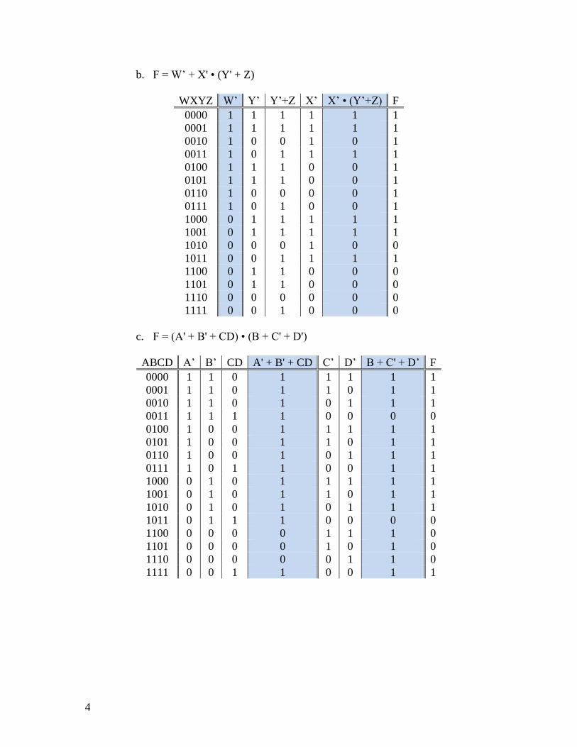
4
b F = Wrsquo + X bull (Y + Z)
WXYZ Wrsquo Yrsquo Yrsquo+Z Xrsquo Xrsquo bull (Yrsquo+Z) F
0000 1 1 1 1 1 1
0001 1 1 1 1 1 1
0010 1 0 0 1 0 1
0011 1 0 1 1 1 1
0100 1 1 1 0 0 1
0101 1 1 1 0 0 1
0110 1 0 0 0 0 1
0111 1 0 1 0 0 1
1000 0 1 1 1 1 1
1001 0 1 1 1 1 1
1010 0 0 0 1 0 0
1011 0 0 1 1 1 1
1100 0 1 1 0 0 0
1101 0 1 1 0 0 0
1110 0 0 0 0 0 0
1111 0 0 1 0 0 0
c F = (A + B + CD) bull (B + C + D)
ABCD Arsquo Brsquo CD A + B + CD Crsquo Drsquo B + C + Drsquo F
0000 1 1 0 1 1 1 1 1
0001 1 1 0 1 1 0 1 1
0010 1 1 0 1 0 1 1 1
0011 1 1 1 1 0 0 0 0
0100 1 0 0 1 1 1 1 1
0101 1 0 0 1 1 0 1 1
0110 1 0 0 1 0 1 1 1
0111 1 0 1 1 0 0 1 1
1000 0 1 0 1 1 1 1 1
1001 0 1 0 1 1 0 1 1
1010 0 1 0 1 0 1 1 1
1011 0 1 1 1 0 0 0 0
1100 0 0 0 0 1 1 1 0
1101 0 0 0 0 1 0 1 0
1110 0 0 0 0 0 1 1 0
1111 0 0 1 1 0 0 1 1
5
d
F = (((Arsquo + B) + C ) + D)
= ((Arsquo + B)rsquo + C) bull Drsquo DEMORGANS
= (A bull Brsquo + Crsquo) bull Drsquo DEMORGANS
= ABrsquoDrsquo + CrsquoDrsquo T8
ABCD Brsquo Drsquo AbullBrsquobullDrsquo Crsquo CrsquobullDrsquo F
0000 1 1 0 1 1 1
0001 1 0 0 1 0 0
0010 1 1 0 0 0 0
0011 1 0 0 0 0 0
0100 0 1 0 1 1 1
0101 0 0 0 1 0 0
0110 0 1 0 0 0 0
0111 0 0 0 0 0 0
1000 1 1 1 1 1 1
1001 1 0 0 1 0 0
1010 1 1 1 0 0 1
1011 1 0 0 0 0 0
1100 0 1 0 1 1 1
1101 0 0 0 1 0 0
1110 0 1 0 0 0 0
1111 0 0 0 0 0 0
4
a
F = XYZ (023)
= m0 + m2 + m3
= XrsquoYrsquoZrsquo + XrsquoYZrsquo + XrsquoYZ
= XYZ (14567)
= M1 bull M4 bull M5 bull M6 bull M7
= (X+Y+Zrsquo)bull(Xrsquo+Y+Z)bull(Xrsquo+Y+Zrsquo)bull(Xrsquo+Yrsquo+Z)bull(Xrsquo+Yrsquo+Zrsquo)
b
F = ABC (1246)
= M1 bull M2 bull M4 bull M6
= (A + B + Crsquo) bull (A + Brsquo + C) bull (Arsquo + B + C) bull (Arsquo + Brsquo + C)
= ABC (0357)
= m0 + m3 + m5 + m7
= ArsquoBrsquoCrsquo + ArsquoBC + ABrsquoC + ABC
6
c
F = ABCD(1257)
= m1 + m2 + m5 + m7
= ArsquoBrsquoCrsquoD + ArsquoBrsquoCDrsquo + ArsquoBCrsquoD +ArsquoBCD
= ABCD (034689101112131415)
= M0 bull M3 bull M4 bull M6 bull M8 bull M8bull M9 bull M10 bull M11 bull M12 bull M13 bull
M14 bull M15
= (A + B + C +D) bull (A + B + Crsquo +Drsquo) bull (A + Brsquo + C +D)
bull (A + Brsquo + Crsquo +D) bull (Arsquo + B + C +D) bull (Arsquo + B + C +Drsquo)
bull (Arsquo + B + Crsquo +D) bull (Arsquo + B + Crsquo +Drsquo) bull (Arsquo + Brsquo + C +D)
bull (Arsquo + Brsquo + C +Drsquo) bull (Arsquo + Brsquo + Crsquo +D) bull (Arsquo + Brsquo + Crsquo +Drsquo)
d
F = X + YZ +YZ = Xrsquo + YZrsquo T3
= Xrsquo(Y + Yrsquo)(Z + Zrsquo) + (X+Xrsquo)(YZrsquo) T1rsquoT5
= XrsquoYrsquoZrsquo + XrsquoYrsquoZ + XrsquoYZrsquo + XrsquoYZ + XYZrsquo + XrsquoYZrsquo T8
= m0 + m1 + m2 + m3 + m6
= XYZ(01236)
= XYZ(457)
= M4 bull M5 bull M7
= (Xrsquo + Y + Z) bull (Xrsquo + Y + Zrsquo) bull (Xrsquo + Yrsquo + Zrsquo)
e
F = AB +BC +ACrsquo
= (ArsquoBC + ArsquoBCrsquo) + (ABrsquoC + ArsquoBrsquoC) + (ABCrsquo + ABrsquoCrsquo) T10
= m3 + m2 + m5 + m1 + m6 + m4
= ABC (123456)
= ABC(07)
= M0 bull M7
= (A + B + C) bull (Arsquo + Brsquo + Crsquo)
5
X + Y X + Yrsquo X
= bull x y x y x y
7
6 One possible solution
XY + XrsquoZ + YZ
XY + XrsquoZ + YZ bull 1 T1rsquo
XY + XrsquoZ + YZ bull (X + Xrsquo) T5
XY + XrsquoZ + XYZ + XYZ T8
(XY + XYZ) + (XrsquoZ + XrsquoZY) T6
XY + XrsquoZ T9
7
a
F = XrsquoZrsquo + (Y(Xrsquo+Z))rsquo
= XrsquoZrsquo + Yrsquo + (Xrsquo+Z)rsquo DEMORGANS
= XrsquoZrsquo + Yrsquo + XZrsquo DEMORGANS
= (Xrsquo + X) bull Zrsquo + Yrsquo T8
= 1 bull Zrsquo + Yrsquo T5
POS = Zrsquo + Yrsquo T1rsquo
b
G = XY + YrsquoZrsquo
= (XY + Yrsquo)(XY + Zrsquo) T8rsquo
= (X + Yrsquo)(Y + Yrsquo)(X + Zrsquo)(Y + Zrsquo) T8rsquo
= (X + Yrsquo)(X + Zrsquo)(Y + Zrsquo) T3rsquo
= (X + Yrsquo)(Y + Zrsquo) T11rsquo
POS = (X + Yrsquo) bull (Y + Zrsquo)
c
H = AB bull (CD)rsquo + A + D
= (AB bull (Crsquo + Drsquo)) + A + D DEMORGANS
= (AB + A + D) bull (Crsquo + Drsquo + A + D) T8rsquo
= (A(B+1) + D) bull (1)
= (A + D) bull 1 T1rsquo
POS = A + D
8
Z = AB + (Crsquo + ArsquoBrsquo)rsquo + Arsquo(AB + ACrsquoDrsquo)
= AB + (Crsquo + ArsquoBrsquo)rsquo + ArsquoAB + ArsquoACrsquoDrsquo T8
= AB + Cbull (A+B) + 0 + 0 DEMORGANS T5rsquo
SOP = AB + AC + BC T8
9
a F = xrsquoyrsquo + xyrsquoz + zrsquo
Let us simplify first
= yrsquo(xrsquo + xz) + zrsquo
= yrsquo(xrsquo(z + zrsquo) + xz) + zrsquo T1rsquo T5
= yrsquo(xrsquoz + xrsquozrsquo + xz) + zrsquo T8
8
= yrsquo(xrsquoz + xrsquoz + xrsquozrsquo + xz) + zrsquo T3 (replicate terms)
= yrsquo(xrsquo(z+zrsquo) + z(xrsquo+x)) + zrsquo T8
= yrsquo(xrsquo +z) + zrsquo T5T1rsquo
Now let us convert to POS using T8rsquo
= (zrsquo+yrsquo)(zrsquo + xrsquo + z) T8rsquo
= (zrsquo+yrsquo) T5T1rsquo
b G = (xrsquo+yrsquo)(y)(wrsquo+y+z)
Convert to SOP using T8 (simplifying as we go)
= (xrsquoy + yrsquoy)(wrsquo + y + z) T8
= xrsquoy(wrsquo + y + z) T5rsquoT1
= wrsquoxrsquoy + xrsquoy + xrsquoyz T8
= xrsquoy(wrsquo + 1 + z) T8
= xrsquoy T2 T1rsquo
9
HW4 - Circuit Design w Karnaugh Maps
1
a F = ABCD(12459101213)
FSOP = CD BC BCD+ +
b F = MNOP(01289)
FSOP = N OP MO+ +
c F = ABCD (01258101115)
1
1
0
1 1
1 1 1 1
3
12 8
9 13 5 1
00 01 11 10
00
01
2 6
7 15
14 10
11
4
11
10
AB
CD
1
1
1
1
1 0
1
1 1
3
12 8
9 13 5 1
00 01 11 10
00
01
2 6
7 15
14 10
11
4
11
10
AB
CD
1
1
1
1
1
1
1
0
1 1
1 1
3
12 8
9 13 5 1
00 01 11 10
00
01
2 6
7 15
14 10
11
4
11
10
MN
OP
10
FSOP = ACD ACD BD+ +
d F = WXYZ (3671214)
FSOP = WY WZ X Z+ +
2
a F = XrsquoYrsquo + XrsquoZrsquo + WrsquoX + XYZ
FPOS = (Wrsquo + Xrsquo + Y)(X + Yrsquo + Zrsquo)(Wrsquo + Xrsquo + Z)
b The 4-bit prime numbers are 2 3 5 7 11 13
FPOS = (C+D)(Brsquo+D)(Arsquo+D)(Arsquo+B+C)
1
1
1
1
1 0
1 1
1 1 1 1
3
12 8
9 13 5 1
00 01 11 10
00
01
2 6
7 15
14 10
11
4
11
10
WX
YZ
0
1
1
1
1
0
0
1
1 0
1 0 1
1 0 1 1
3
12 8
9 13 5 1
00 01 11 10
00
01
2 6
7 15
14 10
11
4
11
10
WX
YZ
1
1
1
0
0
1
0
0 0
0 0 0
0 1 1 0
3
12 8
9 13 5 1
00 01 11 10
00
01
2 6
7 15
14 10
11
4
11
10
AB
CD
11
c The 4-bit numbers that are not perfect squares or cubes are 2 3 5 6 7
10 11 12 13 14 15
FPOS = (B + C)(A + C + D)
d The 4-bit numbers divisible by 3 or 5 are 0 3 5 6 9 10 12 15
FPOS = (A+B+C+Drsquo)(A+B+Crsquo+D)(A+Brsquo+C+D)(A+Brsquo+Crsquo+Drsquo)(Arsquo+B+C+D)bull
(Arsquo+B+Crsquo+Drsquo)(Arsquo+Brsquo+C+Drsquo)(Arsquo+Brsquo+Crsquo+D)
3 The K-Maps are below
FSOP = CD BC BCD+ +
1
1
1
1
1
1
1
1
0 0
0 1 0
0 1 1 0
3
12 8
9 13 5 1
00 01 11 10
00
01
2 6
7 15
14 10
11
4
11
10
AB
CD
1
0
0
1
1
0
0
1
1 0
0 1 0
1 0 1 0
3
12 8
9 13 5 1
00 01 11 10
00
01
2 6
7 15
14 10
11
4
11
10
AB
CD
1
1
0
1 1
1 1 1 1
3
12 8
9 13 5 1
00 01 11 10
00
01
2 6
7 15
14 10
11
4
11
10
AB
CD
12
FPOS = ( )( )( )C D B C B C D+ + + +
a AND ndash OR Implementation
B
Crsquo
D
CDrsquo
Brsquo
b OR - AND Implementation
Drsquo
Crsquo
Brsquo
CD
B
0
0
0
0
0
0
0 0
0
3
12 8
9 13 5 1
00 01 11 10
00
01
2 6
7 15
14 10
11
4
11
10
AB
CD
13
c NAND - NAND Implementation
B
Crsquo
D
CDrsquo
Brsquo
d NOR - NOR Implementation
Drsquo
Crsquo
Brsquo
CD
B
14
4
a The values with an odd number of 1s are 1 2 4 7 8 11 13 14 The
Donrsquot Care numbers are 0 4 5 8 10 12 and 15
SOP = ArsquoCrsquo + BD + AC + BrsquoDrsquo
b F = BrsquoCrsquoDrsquo + BCDrsquo + ABCrsquoD d = ArsquoBCrsquoD + ArsquoBrsquoCDrsquo
F = (A+Arsquo)BrsquoCrsquoDrsquo + (A+Arsquo)BCDrsquo + ABCrsquoD
= ABrsquoCrsquoDrsquo + ArsquoBrsquoCrsquoDrsquo + ABCDrsquo + ArsquoBCDrsquo + ABCrsquoD
d = ArsquoBCrsquoD + ArsquoBrsquoCDrsquo
FSOP = BrsquoCrsquoDrsquo + BCrsquoD + BCDrsquo
1
1
d
1
1
d
d 0
1 d 1
1 d 1
3
12 8
9 13 5 1
00 01 11 10
00
01
2 6
7 15
14 10
11
4
11
10
AB
CD
d
1
1
1 0
1
1 d
3
12 8
9 13 5 1
00 01 11 10
00
01
2 6
7 15
14 10
11
4
11
10
AB
CD
15
5
a F = ArsquoC + ACE + CABrsquo + BrsquoArsquoDE + Arsquo Drsquo Ersquo
FSOP = ArsquoC + ArsquoDrsquoErsquo + ArsquoBrsquoDE + BrsquoC + CE
b F = (AB + ArsquoBrsquo) (CrsquoDrsquo + CD)
= ABCrsquoDrsquo + ArsquoBrsquoCrsquoDrsquo + ABCD + ArsquoBrsquoCD
bull K-Map
FSOP = ABCrsquoDrsquo + ArsquoBrsquoCrsquoDrsquo + ABCD + ArsquoBrsquoCD
1
1
1 0
1
3
12 8
9 13 5 1
00 01 11 10
00
01
2 6
7 15
14 10
11
4
11
10
AB
CD
1
0
1
1
1
1
0
0
1 0
1 1 1
0 1 1
3
12 8
9 13 5 1
00 01 11 10
00
01
2 6
7 15
14 10
11
4
11
10
BC
DE
0
0
1
1
1
0
0
0
0 0
1 0 0
0 1 1 0
3
12 8
9 13 5 1
00 01 11 10
00
01
2 6
7 15
14 10
11
4
11
10
BC
DE
A=0 A=1
16
bull NAND ndash NAND Implementation
B
Crsquo
Drsquo
D
C
A
Arsquo
Brsquo
c F = ArsquoBrsquoCrsquoDrsquo + ArsquoBrsquoCDrsquo + ArsquoBCrsquoDrsquo + ArsquoBCrsquoD + ABrsquoCDrsquo
bull K-Map
FSOP = ArsquoCrsquoDrsquo + ArsquoBCrsquo + BrsquoCDrsquo
bull NAND ndash NAND Implementation
ArsquoCrsquo
Drsquo
B
Brsquo
C
1
1
1 0
1
1
3
12 8
9 13 5 1
00 01 11 10
00
01
2 6
7 15
14 10
11
4
11
10
AB
CD
F
F
17
d The numbers are 2 3 4 5 10 12 13 14 15
bull K-Map
SOP = AB + BCrsquo + ArsquoBrsquoC + ACDrsquo
bull NAND ndash NAND Implementation
A
B
Crsquo
ArsquoBrsquoC
Drsquo
1
1
1
1
1
0
1 1
1 1
3
12 8
9 13 5 1
00 01 11 10
00
01
2 6
7 15
14 10
11
4
11
10
AB
CD
18
6
a F = ArsquoC + ACE + CABrsquo + BrsquoArsquoDE + Arsquo Drsquo Ersquo
bull K-Map
FPOS = (Arsquo + Crsquo)(Arsquo + Brsquo + E)(Brsquo+C+Ersquo)(C + D + Ersquo)(C + Drsquo + E)
b F = (AB + ArsquoBrsquo) (CrsquoDrsquo + CD)
bull K-Map
FPOS = (A + Brsquo)(Arsquo + B)(C + Drsquo)(Crsquo + D)
0
0
0
0
0
0
0
0 0
0 0 0 0
3
12 8
9 13 5 1
00 01 11 10
00
01
2 6
7 15
14 10
11
4
11
10
AB
CD
1
0
1
1
1
1
0
0
1 0
1 1 1
0 1 1 0
3
12 8
9 13 5 1
00 01 11 10
00
01
2 6
7 15
14 10
11
4
11
10
BC
DE
0
0
1
1
1
0
0
0
0 0
1 0 0
0 1 1 0
3
12 8
9 13 5 1
00 01 11 10
00
01
2 6
7 15
14 10
11
4
11
10
BC
DE
A=0 A=1
19
NOR ndash NOR Implementation
A
Brsquo
Arsquo
B
CDrsquo
Crsquo
D
c F = ArsquoBrsquoCrsquoDrsquo + ArsquoBrsquoCDrsquo + ArsquoBCrsquoDrsquo + ArsquoBCrsquoD + ABrsquoCDrsquo
bull K-Map
FPOS = (B + Drsquo)(Brsquo + Crsquo)(Arsquo + C)
bull NOR ndash NOR Implementation
B
Drsquo
BrsquoCrsquo
ArsquoC
0
0
0
0
0
0
0
0 0
0 0 0
3
12 8
9 13 5 1
00 01 11 10
00
01
2 6
7 15
14 10
11
4
11
10
AB
CD
F
F
20
d The numbers are 2 3 4 5 10 12 13 14 15
bull K-Map
POS = (B + C)(A + Brsquo + Crsquo)(Arsquo + B + Drsquo)
bull NOR ndash NOR Implementation
BC
ABrsquoCrsquo
Arsquo
Drsquo
7 A and B are both 2-bit signed numbers They range from -2 to +1 Thus F = A + B
is ranging from -4 to +2 We need 3 bits to represent the signed number F
a The block diagram is below
A1
A0
B1
B0
F2
F1
F0
0
0
0
0 0
0
0 0
3
12 8
9 13 5 1
00 01 11 10
00
01
2 6
7 15
14 10
11
4
11
10
AB
CD
F
21
b The truth table is below
A1 A0 B1 B0 F2 F1 F0
0 0 0 0 0 0 0
0 0 0 1 0 0 1
0 0 1 0 1 1 0
0 0 1 1 1 1 1
0 1 0 0 0 0 1
0 1 0 1 0 1 0
0 1 1 0 1 1 1
0 1 1 1 0 0 0
1 0 0 0 1 1 0
1 0 0 1 1 1 1
1 0 1 0 1 0 0
1 0 1 1 1 0 1
1 1 0 0 1 1 1
1 1 0 1 0 0 0
1 1 1 0 1 0 1
1 1 1 1 1 1 0
c
K-Map of output ldquoF2rdquo K-Map of output ldquoF1rdquo
F2SOP = A1A0rsquo + B1B0rsquo + A1B1 + A1B0rsquo + A0rsquoB1
F1SOP = A1B1rsquoB0rsquo + A1A0rsquoB1rsquo + A1rsquoA0rsquoB1 + A1rsquoB1B0rsquo + A1rsquoA0B1rsquoB0 + A1A0B1B0
1
1
1
1
1
1
1
0
1 1
1
3
12 8
9 13 5 1
00 01 11 10
00
01
2 6
7 15
14 10
11
4
11
10
A1A0
B1B0
1
1
1
1
0
1 1
1 1
3
12 8
9 13 5 1
00 01 11 10
00
01
2 6
7 15
14 10
11
4
11
10
A1A0
B1B0
22
K-Map of output ldquoF0rdquo
F0SOP = A0B0rsquo + A0rsquoB0
d AND-OR implementation
Implementation of F2
A1A0
B1
B0
Implementation of F1
The implementation consists of four 3-input AND gates two 4-input AND gates and one
6-input OR gate
Implementation of F0
A0B0
A0
B0
1
1
1
1
0
1 1
1 1
3
12 8
9 13 5 1
00 01 11 10
00
01
2 6
7 15
14 10
11
4
11
10
A1A0
B1B0
23
NAND ndash NAND Implementation
(1) Implementation of F2
A1A0
B1
B0
(2) Implementation of F1
The implementation consists of four 3-input NAND gates two 4-input NAND gates and
one 6-input NAND gate
(3) Implementation of F0
A0B0
A0
B0
24
8 X is a 3-bit unsigned number It ranges from 0 to 7 Thus Y = 3X + 1 is ranging
from 1 to 22 We need 5 bits to represent the unsigned number Y
a The block diagram is below
X2
X1
X0
Y4
Y3Y2
Y1
Y0
b The truth table is below
X X2 X1 X0 Y4 Y3 Y2 Y1 Y0 Y
0 0 0 0 0 0 0 0 1 1
1 0 0 1 0 0 1 0 0 4
2 0 1 0 0 0 1 1 1 7
3 0 1 1 0 1 0 1 0 10
4 1 0 0 0 1 1 0 1 13
5 1 0 1 1 0 0 0 0 16
6 1 1 0 1 0 0 1 1 19
7 1 1 1 1 0 1 1 0 22
c
K-Map of output ldquoY4rdquo K-Map of output ldquoY3rdquo
Y4POS = X2(X1 + X0) Y3POS = (X2 + X1)(X1rsquo + X0)(X2rsquo + X0rsquo)
K-Map of output ldquoY2rdquo
Y2POS = (X2 + X1 + X0)( X2 + X1rsquo + X0rsquo)( X2rsquo + X1rsquo + X0)( X2rsquo + X1 + X0rsquo)
0 0
0 0
0 0
6 4
5 7 3 1
00 01 11 10
0
1
2
X2X1
X0
0 0
0 0
0 0 0
6 4
5 7 3 1
00 01 11 10
0
1
2
X2X1
X0
0 0
0
0 0
6 4
5 7 3 1
00 01 11 10
0
1
2
X2X1
X0
25
K-Map of output ldquoY1rdquo K-Map of output ldquoY0rdquo
Y1POS = X1 Y0POS = X0rsquo
d
bull OR ndash AND Implementation
Implementation of Y4
X1
X0
X2
Implementation of Y3
X2
X1
X1
X0
X2
X0
0 0
0
0 0
6 4
5 7 3 1
00 01 11 10
0
1
2
X2X1
X0
0
0 0 0 0
6 4
5 7 3 1
00 01 11 10
0
1
2
X2X1
X0
26
Implementation of Y2
X2X1X0
X1
X0
X2
Implementation of Y1 (straight wire connection)
Y1X1
Implementation of Y0 (straight wire connection)
Y0X0
bull NOR ndash NOR Implementation
Convert all gates in the above implementations to NOR gates For Y1 and Y0 just use
wires
27
e This will not be covered at this point of the class since we have not yet discussed
adders Ignore this question
9 X is a 3-bit signed number It ranges from -4 to +3
Thus Z = X2 + 2X + 1 = (X + 1)2 is ranging from 0 to +16 We need 6 bits to
represent signed number Z
a The block diagram is below
Z5
Z4
Z3
Z2Z1
Z0
X0
X1
X2
b The truth table is below
X X2 X1 X0 Z5 Z4 Z3 Z2 Z1 Z0 Z
+0 0 0 0 0 0 0 0 0 1 +1
+1 0 0 1 0 0 0 1 0 0 +4
+2 0 1 0 0 0 1 0 0 1 +9
+3 0 1 1 0 1 0 0 0 0 +16
-1 1 1 1 0 0 0 0 0 0 +0
-2 1 1 0 0 0 0 0 0 0 +1
-3 1 0 1 0 0 0 0 0 0 +4
-4 1 0 0 0 0 1 0 0 1 +9
c
No K-Map needed for Z5 ldquoZ5rdquo = 0
K-Map of output ldquoZ4rdquo K-Map of output ldquoZ3rdquo
Z4SOP = X2rsquoX1X0 Z3SOP = X2rsquoX1X0rsquo + X2X1rsquoX0rsquo
0
1
6 4
5 7 3 1
00 01 11 10
0
1
2
X2X1
X0
0
1 1
6 4
5 7 3 1
00 01 11 10
0
1
2
X2X1
X0
28
K-Map of output ldquoZ2rdquo K-Map of output ldquoZ0rdquo
Z2SOP = X2rsquoX1rsquoX0 Z0SOP = X2rsquoX0rsquo + X1rsquoX0rsquo
Note Z1 = 0 (constant)
0
1
6 4
5 7 3 1
00 01 11 10
0
1
2
X2X1
X0
1 0
1 1
6 4
5 7 3 1
00 01 11 10
0
1
2
X2X1
X0
29
10 Design a 1-bit comparator that takes in a bit X and a bit Y and outputs XltY
XgtY X=Y Use a single 2-to-4 decoder and 1 single OR gate
Consider the truth table of each of these simple functions We can implement
each as a sum of minterms And since a decoder implements the minterms of
the input variables we can arrive at the circuit above
X Y XltY XgtY X==Y
0 0 0 0 1
0 1 1 0 0
1 0 0 1 0
1 1 0 0 1
Y0
Y1
Y2
Y3
A0
A1
2-t
o-4
Decoder
X
Y XltY
XgtY
X=Y
30
HW5 - Signed Representations and Arithmetic
1
a
11 1
10100 = 20
+ 11101 = 29
Carry=1 110001 = 49
b
11100
- 10100
01000
28
- 20
8
1 1 1 1 _
11100
2rsquos comp 01011
+ 1
01000
2
b
1 1 1 1 _
101011
+ 011010
1000101
3 For unsigned subtraction we still use take the 2s complement of the bottom
number (but the check for overflow differs for unsigned vs 2s complement)
a 01101102 ndash 01001002 cannot be performed as is because we cannot
subtract a larger number from a smaller number in unsigned
representation
0110110
- 0100100
+54
-60
-6
1 1 1 1 1 1 _
0110110
2rsquos comp 1011011
+ 1
0010010
4
a Unsigned binary 28 lt 28310 lt 29 Therefore 9 bits 28310 = 1000110112
b 2rsquos complement with n-bits we can make ndash(2n-1) to +(2n-1-1) With n = 9
the range is -256 to +256 With n = 10 the range is -512 to +511 Thus
10 bits 28310 = 1000110112
5 Consider the following decimal numbers +21 +55 +121 -32 -99 -128
a What are the corresponding 8-bit signed-magnitude representation
31
a What are the corresponding 8-bit 2s complement representation
b Which of the above numbers can be represented in 6-bit signed-
magnitude 6-bit 1s complement 6-bit 2s complement representations
explain
21 55 121 -32 -99 -128 A 16+4+1=21
00010101 00110111 01111001 10100000 11100011 NA
B 00010101 00110111 01111001 1110000 10011101 10000000 C YYY
010101 in all cases
NNN NNN NNY 100000 in 2rsquos comp
NNN NNN
6 What are the corresponding decimal representations for the following binary
numbers 01011011 11010010 if
a The binary numbers are in 8-bit signed-magnitude format
b The binary numbers are in 8-bit 2s complement format
01011011 11010010 a) 64+16+8+2+1=91 -(64+16+2)=-82 b) 64+16+8+2+1=91 -128+64+16+2=-46
7 Perform the following addition problems for the following 2rsquos complement
numbers State whether overflow does or does not occur for each problem
Justify your answer for why overflow does or does not occur Check your
work by converting each number to decimal
a 1010 0111 b 1001 0110 c 0101 1100 d 0101 1101
+1110 0100 +1011 0011 +1011 0101 +0110 1001
11000 1011 10100 1001 10001 0001 1100 0110
n+n=n
cin=cout=1
No Overflow
n+n=p
cin=0cout=1
Overflow
p+n=p
cin=cout=1
NoOverflow
p+p=n
cin=1cout=0
Overflow
8 This is an exercise to help you remember what gates are used to create a full
adder Using a full adder as shown below and no other gates can you
produce the function Z = AbullB (Hint Write out the logical equations for S
and Cout and see if you can hook up the inputs to produce Z)
ANSWER
Cin X Y S Cout
0 0 0 0 0
32
0 0 1 1 0
0 1 0 1 0
0 1 1 0 1
1 0 0 1 0
1 0 1 0 1
1 1 0 0 1
1 1 1 1 1
S X Y Cin
Cout XY XCin YCin
=
= + +
We want Z=XY and if we set Cin=0 then the formulas of S and Cout
becomes as follows
S X Y
Cout XY
=
=
Thus Cout = Z = XY
X Y
S
CinFull Adder
Cout
A B
0Z
33
9 Using 1 half-adder and a minimal number of 4-bit binary adders design a
circuit to calculate Y = 25X where X is a 4-bit inputs
ANSWER
If a number is multiplied by a number that is a power of 2 then the number rewritten
using the above formula
2 00
n
n X X=
Y = 25X = 16X + 8X + X = X0000+X000+X
Also adding the information that X is a 4-bit number above formula can be re-written
X = X3X2X1X0
Y = X3X2X1X00000 + X3X2X1X0000 + X3X2X1X0
This can be written as addition by 4 bit adders
X3 X2 X1 X0
X3 X2 X1 X0 0 0 0
+ X3 X2 X1 X0 0 0 0 0
Since one row in each addition is all zeros they can be eliminated and the other two
numbers can be added using a 4-bit adder However the lower bits require only a single
bit adder The carry from the first addition is transferred to the next one
B3 B2 B1 B0 A3 A2 A1 A0
S0S1S2S3
C0C4 4-bit Binary Adder
X Y
S
Half AdderCout
X3 X0X0X1X2X3 X1X2X30 X0X1X2
Y8 Y7 Y6 Y5 Y4 Y3 Y0Y1Y2
34
10 Using a minimal number of 4-bit adders design a circuit that implements
Y=20X+107 where X is a 3-bit unsigned number
ANSWER
X = X2X1X0 and thus 20X= 16X+4X These numbers are achieved by inserting zeros
at the end Once we add these there numbers we see that not all bits require addition We
actually need only a single 4-bit adder and nothing more
1 1 0 1 0 1 1
X2 X1 X0 0 0
+ X2 X1 X0 0 0 0 0
Which can be collapsed to the following addition
1 1 X2 X1 X0 0 0
+ X2 X1 X0 1 0 1 1
B3 B2 B1 B0 A3 A2 A1 A0
S0S1S2S3
C0C4 4-bit Binary Adder
X0X1X2 X1X211
11
X0
Y7 Y6 Y5 Y4 Y3 Y0Y1Y2
0
1
35
11 Design a minimal circuit using ANDORNOT gates to implement the
comparison A gt 10 where A is a 4-bit number
a Start by writing out the logical algorithm for when A gt 10 then implement it
using gates
b Check that your work is minimal by using a K-Map
ANSWER
Letrsquos assume that the number A = A3A2A1A0
Logical Algorithm For any number A to be greater than a number B (in this case 1010 =
10102) a more significant bit of A must be greater than B However in the case of A
compared with 1010 we realize A3 and A1 can never be greater than the 1rsquos in those
places for 10 Similarly A2 and A0 can never be less than the 0rsquos in those places Thus
for A gt 10 there are only 2 cases that need to be checked
A3 = 1 and A2 gt 0 (ie A2 = 1)
OR
A3=1 and A1 = 1 and A0 gt 0 (ie A0 = 1)
Thus Agt10 = A3A2 + A3A2A0
Note that we donrsquot have to check A2 in the second case because it is DEFINITELY
greater than or equal to the 0 in that place of 10102
A K-Map will also show the same equation
SUM(1112131415)
Agt10=A3A2+ A3A1A0
A3
A2
A3
A0A1
Agt10
1
1
1
0
1
1
3
12 8
9 13 5 1
00 01 11 10
00
01
2 6
7 15
14 10
11
4
11
10
A3A2
A1A0
36
HW 6 ndash Latches and Flip-Flops
1 Complete the following waveforms for negative edge-triggered D Flip-Flops
D Q
QCK
D Q
QCK
CLK
D1
D2D1
D2
Z
X
CLK
X
D1
D2
Z
2 We should find the state diagram following the steps in the class notes
a Convert the diagram to a table
Current
State
Next State Output
XY= 00 XY= 01 XY= 10 XY= 11
Q1 Q0 Q1 Q0
Q1
Q0 Q1
Q0 Q1
Q0 Z
0 0 0 0 0 0 1 0 1 0 0
0 1 0 0 0 0 0 1 0 1 1
1 0 0 0 0 1 0 0 0 1 0
1 1 0 0 0 1 0 1 0 1 0
37
Convert Q to D
Current
State
Next State Output
XY= 00 XY= 01 XY= 10 XY= 11
Q1 Q0 D1 D0 D1 D0 D1 D0 D1 D0 Z
0 0 0 0 0 0 1 0 1 0 0
0 1 0 0 0 0 0 1 0 1 1
1 0 0 0 0 1 0 0 0 1 0
1 1 0 0 0 1 0 1 0 1 0
b Perform K-maps to find equations for D1 and D0
D0 = Q1Y + Q0X
D1 = Q1rsquoQ0rsquoX
c Draw the circuit and implement the initial state (reset) condition
D Q
QCK
D Q
QCK
ZX
Clock
Q0
Q1Y
PRE PRE
CLR CLR
Reset Reset
GND GND
38
3 Because we have 2 states in the state diagram we use one D flip-flop to
implement state memory We design the combinational logic for the next-state
logic and the output function logic by building up the statetransition table
Current State Next State Output
XY = 00 XY = 01 XY = 10 XY = 11
SymbolCode SymbolCode SymbolCode SymbolCode SymbolCode H
F 0 F 0 G 1 G 1 G 1 0
G 1 F 0 F 0 F 0 G 1 1 Q0(t) Q0
D0 Q0
D0 Q0
D0 Q0
D0
After we get the statetransition table we build the K-Maps to simplify expressions for
D0 and H
bull D0 K-Map
D0 = YQ0rsquo + XQ0rsquo + XY H = Q0
0
1 1 1
1
6 4
5 7 3 1
00 01 11 10
0
1
2
XY
Q0
39
4
Current State Next State amp Flop-Flop Inputs Outputs
Next State Next State
X = 0 X = 1
SymbolCode SymbolCode SymbolCode Z
A00 B01 D11 0
B01 C10 B01 0
C10 B01 A00 1
D11 B01 C10 0 Q1(t)Q0(t) Q1(t+1)Q0(t+1) Q1(t+1)Q0(t+1)
After we get the statetransition table we build the K-Maps to simplify expressions for
D1 D0 and Z
bull D1 K-Map D0 K-Map
D1 = XrsquoQ1Q0 + XQ0rsquo D0 = XrsquoQ1+XQ0 + XQ1rsquo
Z K-Map
Z = Q1Q0rsquo
1
1 0
0 1
1 0
1 00
01
11
10
0 Q1Q0
X
1
1
0 0
1 0
0 1
0 00
01
11
10
0 Q1Q0
X
1
1
0 0
0 0
1
0 Q0
Q1
1
40
a The waveform is below
CLK
X
Q1
Q0
State
Z
A D B C A B
41
5
a We need 4 states and each of them stores one 2-bit binary number ranging
from 00 to 11
State S0 S1 S2 S3
Assignment
(Q1 Q0)
00 01 10 11
The state diagram is below
b Because we have 4 states in the state diagram we use two D flip-flops to
implement state memory We design the combinational logic for the next-
state logic and the output function logic by building up the statetransition
table
U ndash UP D ndash DOWN
Current State Next State
UD = 00 UD = 01 UD = 10 UD = 11
SymbolCode SymbolCode SymbolCode SymbolCode SymbolCode
S000 S000 S311 S101 S000
S101 S101 S000 S210 S101
S210 S210 S101 S311 S210
S311 S311 S210 S000 S311 Q1(t)Q0(t) Q1(t+1)Q0(t+1)
D1D0 Q1(t+1)Q0(t+1)
D1D0 Q1(t+1)Q0(t+1)
D1D0 Q1(t+1)Q0(t+1)
D1D0
After we get the statetransition table we build the K-Maps to simplify expressions for
D1 and D0
S0 S1 S2 S3
UP=DOWN=1 or
UP=DOWN=0
UP=DOWN=1 or
UP=DOWN=0
UP=DOWN=1 or
UP=DOWN=0UP=DOWN=1 or
UP=DOWN=0
UP=1 and
DOWN=0
UP=1 and
DOWN=0UP=1 and
DOWN=0
UP=1 and DOWN=0
UP=0 and
DOWN=1UP=0 and
DOWN=1
UP=0 and
DOWN=1
UP=0 and DOWN=1
~R
ese
t
42
bull D1 K-Map
D1 = UrsquoDrsquoQ1 + DQ1Q0 + UQ1Q0rsquo + UrsquoDQ1rsquoQ0rsquo + UDrsquoQ1rsquoQ0
bull D0 K-Map
D0 = UrsquoDrsquoQ0 + UDQ0 + UrsquoDQ0rsquo + UDrsquoQ0rsquo
c The waveform is below
CLK
UP
DOWN
Q1
Q0
1
1
1
1
1
1
0
1
1
3
12 8
9 13 5 1
00 01 11 10
00
01
2 6
7 15
14 10
11
4
11
10
UD
Q1Q0
1
1
1
1
0
1 1
1 1
3
12 8
9 13 5 1
00 01 11 10
00
01
2 6
7 15
14 10
11
4
11
10
UD
Q1Q0
43
6 Complete the waveform for the 4-bit counter presented in class
1111
Clock
SR
CEP
CET
PE
P3-P0
Q3-Q0 1101
1101
1110 0000 0001 0000 1110 1111
7 Complete the waveform for a 4-bit D-Register with Data (Load) Enable and
asynchronous reset
CLK
AR
EN
0110D[30] 0001 10111010 11011001 10001111 0111
Q[30] 1010 11111101 10000000 1011
44
81 Unit 7 ndash Datapath Design 1 Implement a circuit that takes in a 4-bit number X[30] and produces a 4-bit value
Z[30] according to the following function
if X lt 8 then
Z = X + 5
else
Z = X ndash 2
Using the building blocks below and at most 1 inverter (no other gates)
implement this function
Note To check Xlt8 subtract X-8 by taking the 2rsquos complement of 8 The 2rsquos comp of
8 is 0111+1 Recall a carry of 0 when subtracting unsigned numbers (A-B) indicates
overflow which can only occur in unsigned subtraction if the result needed to be negative
(ie A lt B) So C4 will only be 1 if X is not less-than 8 We can invert it to get a signal
that is true when X lt 8 Use those signals to either add 5 (0101) or subtract 2 (add 1110)
B3 B2 B1 B0 A3 A2 A1 A0
S0S1S2S3
C0C4 4-bit Binary Adder
X lt 8
Xlt8
X0X1X2X3
Z0Z1Z2Z3
B3
B2
B1
B0
A3
A2
A1
A0
S0
S1
S2
S3
C0
C4
4-b
it B
inary
Add
er
X3
X2
X1
X0
1
1
1
0
1
0
1
45
2 Design a circuit that takes in an 4-bit number X[30] and outputs a number Y and
performs the operation below Assume these numbers are unsigned Use a 4-bit
adder and 2-to-1 muxes Hint Multiplying by 4 (ie 22) in binary can be done with
no gates just as multiplying by 100 (ie 102) in decimal can be done simply and
easily
if(X lt 00112)
Y = 4X
else
Y = X
4X would require 6 outputs and be X3 X2 X1 X0 0 0 thus even if we pass X we need to
produce 6 outputs Recall subtracting 3=0011 bin is the same as adding the 2s
complement Next a carry of 0 when subtracting unsigned numbers (A-B) indicates
overflow which can only occur in unsigned subtraction if the result needed to be negative
(ie A lt B)
I1
Y
S
I0
I1
Y
S
I0
I1
Y
S
I0
I1
Y
S
I0
I1
Y
S
I0
I1
Y
S
I0
X0
X1
X2
X3
0
0
0
0
X0
X1
X2
X3
Y5
Y4
Y3
Y2
Y0
Y1
X lt 3
B3
B2
B1
B0
A3
A2
A1
A0
S0
S1
S2
S3
C0
C4
4-b
it B
inary
Add
er
X3
X2
X1
X0
0
0
1
1
1
46
3 Design a circuit that takes in two 4-bit numbers X[30] and Y[30] along with two
function select bits FS1 and FS0 and produces an output Z[30] according to the
following table
FS1FS0 Z
00 X+Y
01 X-Y
10 Y-X
11 donrsquot care
Use (1) 4-bit adder 4-bit wide 2-to-1 muxes and any basic gates you desire
Approach Take a 4-bit adder and for each operation listed in the table above
identify what should be passed to the A and B inputs of the adder Then use
muxes to perform that function Design logic for the select bits of the muxes and
the carry-in of the adder that use FS1 and FS0 as input
Note In the solution below the A and B inputs of the muxes are like the 0th and
1st inputs of 4 2-to-1 muxes respectively Ignore the G input
B3
B2
B1
B0
A3
A2
A1
A0
S3
S2
S1
S0
C0
C4
S
G
1A
1Y
2Y
2-to-1
4-bit
wide
mux
2A
3A
4A3Y
4Y1B
2B
3B
4B
0
S
G
1A
1Y
2Y
2-to-1
4-bit
wide
mux
2A
3A
4A3Y
4Y1B
2B
3B
4B
0
X3
X2
X1
X0
X3
X2
X1
X0
Y3
Y2
Y1
Y0
Y3
Y2
Y1
Y0
Z3
Z2
Z1
Z0
FS1
FS0
FS1FS0
74LS
283
47
4 Design a circuit that takes in two 4-bit signed magnitude numbers X[30] and
Y[30] and produces two 4-bit outputs A[30] and B[30] according to the following
algorithm
if X gt= Y then
A = X and B = Y
else
A = Y and B = X
Use a 4-bit adder to subtract and perform the comparison 4-bit wide 2-to-1
muxes and basic logic gates Assume the input 1000 = -0 will never occur on X
or Y
Approach First think about how to compare signed magnitude numbers by using
unsigned comparison techniques and how to precondition the inputs to allow the
use of unsigned comparison For example 1001 = -1 in signed magnitude and
0100 = +4 in signed magnitude So 1001 is really less than 0100 Use the
comparison result to control the selects of the muxes
Y0
Y1
Y2
Y3
X0
X1
X2
X3
XgtY
S
G
1A
1Y
2Y
2-to-1
4-bit
wide
mux
2A
3A
4A3Y
4Y1B
2B
3B
4B
0
S
G
1A
1Y
2Y
2-to-1
4-bit
wide
mux
2A
3A
4A3Y
4Y1B
2B
3B
4B
0
X3
X2
X1
X0
Y3
Y2
Y1
Y0
X3
X2
X1
X0
Y3
Y2
Y1
Y0
A3
A2
A1
A0
B3
B2
B1
B0
B3
B2
B1
B0
A3
A2
A1
A0
S0
S1
S2
S3
C0
C4
4-b
it B
inary
Add
er
1
48
5 Design a circuit that adds two 4-bit unsigned numbers X[30] and Y[30] and
outputs either the sum if there is no overflow or 1111 (=1510 the maximum unsigned
4-bit number) if there is overflow
Unsigned overflow is found by looking at Cout You could use a mux to select the sum
or 1111 but realize you can just use OR gates for this function
B3
B2
B1
B0
A3
A2
A1
A0
S3
S2
S1
S0
C0
C4
74LS
283
X3
X2
X1
X0
UNS_OV
0
Y3
Y2
Y1
Y0
G0
G1
G2
G3
49
1 We would like to build an adder whose inputs are in units of pennies and produces
sum in nickels and pennies Essentially this is a base-5 adder The 2 inputs of this
adder are A=A2A1A0 and B=B2B1B0 Assume that the maximum input number
that A and B can be is 4 pennies Design an adder to produce the correct
nickelspennies sum C= [CN] [CP2CP1CP0] To implement this design you may
assume you can use as many 4-bit adders as you like
if X+Y gt 4 dec then
CN = 1 CP[20] = X+Y-5
else
CN = 0 CP[20] = X+Y
A2 A1 A0 B2 B1 B0
CP2 CP1 CP0
To be designed by you
CN
Block diagram for the
nickelpenny adder you
are going to design
50
B3 B2 B1 B0 A3 A2 A1 A0
S0S1S2S3
C0C4 4-bit Binary Adder
Z4 Z2 Z1
CP2
0
0
B3 B2 B1 B0 A3 A2 A1 A0
S0S1S2S3
C0C4 4-bit Binary Adder
0 X4 X2 X1 0 Y4 Y2 Y1
Z8 Z4 Z2 Z1
0
B3 B2 B1 B0 A3 A2 A1 A0
S0S1S2S3
C0C4 4-bit Binary Adder
0 1 0 0 Z8 Z4 Z2 Z1
1
Need actual
inverters here
just didn t
draw them
CN
(4 lt X+Y)
CP1 CP0

5
d
F = (((Arsquo + B) + C ) + D)
= ((Arsquo + B)rsquo + C) bull Drsquo DEMORGANS
= (A bull Brsquo + Crsquo) bull Drsquo DEMORGANS
= ABrsquoDrsquo + CrsquoDrsquo T8
ABCD Brsquo Drsquo AbullBrsquobullDrsquo Crsquo CrsquobullDrsquo F
0000 1 1 0 1 1 1
0001 1 0 0 1 0 0
0010 1 1 0 0 0 0
0011 1 0 0 0 0 0
0100 0 1 0 1 1 1
0101 0 0 0 1 0 0
0110 0 1 0 0 0 0
0111 0 0 0 0 0 0
1000 1 1 1 1 1 1
1001 1 0 0 1 0 0
1010 1 1 1 0 0 1
1011 1 0 0 0 0 0
1100 0 1 0 1 1 1
1101 0 0 0 1 0 0
1110 0 1 0 0 0 0
1111 0 0 0 0 0 0
4
a
F = XYZ (023)
= m0 + m2 + m3
= XrsquoYrsquoZrsquo + XrsquoYZrsquo + XrsquoYZ
= XYZ (14567)
= M1 bull M4 bull M5 bull M6 bull M7
= (X+Y+Zrsquo)bull(Xrsquo+Y+Z)bull(Xrsquo+Y+Zrsquo)bull(Xrsquo+Yrsquo+Z)bull(Xrsquo+Yrsquo+Zrsquo)
b
F = ABC (1246)
= M1 bull M2 bull M4 bull M6
= (A + B + Crsquo) bull (A + Brsquo + C) bull (Arsquo + B + C) bull (Arsquo + Brsquo + C)
= ABC (0357)
= m0 + m3 + m5 + m7
= ArsquoBrsquoCrsquo + ArsquoBC + ABrsquoC + ABC
6
c
F = ABCD(1257)
= m1 + m2 + m5 + m7
= ArsquoBrsquoCrsquoD + ArsquoBrsquoCDrsquo + ArsquoBCrsquoD +ArsquoBCD
= ABCD (034689101112131415)
= M0 bull M3 bull M4 bull M6 bull M8 bull M8bull M9 bull M10 bull M11 bull M12 bull M13 bull
M14 bull M15
= (A + B + C +D) bull (A + B + Crsquo +Drsquo) bull (A + Brsquo + C +D)
bull (A + Brsquo + Crsquo +D) bull (Arsquo + B + C +D) bull (Arsquo + B + C +Drsquo)
bull (Arsquo + B + Crsquo +D) bull (Arsquo + B + Crsquo +Drsquo) bull (Arsquo + Brsquo + C +D)
bull (Arsquo + Brsquo + C +Drsquo) bull (Arsquo + Brsquo + Crsquo +D) bull (Arsquo + Brsquo + Crsquo +Drsquo)
d
F = X + YZ +YZ = Xrsquo + YZrsquo T3
= Xrsquo(Y + Yrsquo)(Z + Zrsquo) + (X+Xrsquo)(YZrsquo) T1rsquoT5
= XrsquoYrsquoZrsquo + XrsquoYrsquoZ + XrsquoYZrsquo + XrsquoYZ + XYZrsquo + XrsquoYZrsquo T8
= m0 + m1 + m2 + m3 + m6
= XYZ(01236)
= XYZ(457)
= M4 bull M5 bull M7
= (Xrsquo + Y + Z) bull (Xrsquo + Y + Zrsquo) bull (Xrsquo + Yrsquo + Zrsquo)
e
F = AB +BC +ACrsquo
= (ArsquoBC + ArsquoBCrsquo) + (ABrsquoC + ArsquoBrsquoC) + (ABCrsquo + ABrsquoCrsquo) T10
= m3 + m2 + m5 + m1 + m6 + m4
= ABC (123456)
= ABC(07)
= M0 bull M7
= (A + B + C) bull (Arsquo + Brsquo + Crsquo)
5
X + Y X + Yrsquo X
= bull x y x y x y
7
6 One possible solution
XY + XrsquoZ + YZ
XY + XrsquoZ + YZ bull 1 T1rsquo
XY + XrsquoZ + YZ bull (X + Xrsquo) T5
XY + XrsquoZ + XYZ + XYZ T8
(XY + XYZ) + (XrsquoZ + XrsquoZY) T6
XY + XrsquoZ T9
7
a
F = XrsquoZrsquo + (Y(Xrsquo+Z))rsquo
= XrsquoZrsquo + Yrsquo + (Xrsquo+Z)rsquo DEMORGANS
= XrsquoZrsquo + Yrsquo + XZrsquo DEMORGANS
= (Xrsquo + X) bull Zrsquo + Yrsquo T8
= 1 bull Zrsquo + Yrsquo T5
POS = Zrsquo + Yrsquo T1rsquo
b
G = XY + YrsquoZrsquo
= (XY + Yrsquo)(XY + Zrsquo) T8rsquo
= (X + Yrsquo)(Y + Yrsquo)(X + Zrsquo)(Y + Zrsquo) T8rsquo
= (X + Yrsquo)(X + Zrsquo)(Y + Zrsquo) T3rsquo
= (X + Yrsquo)(Y + Zrsquo) T11rsquo
POS = (X + Yrsquo) bull (Y + Zrsquo)
c
H = AB bull (CD)rsquo + A + D
= (AB bull (Crsquo + Drsquo)) + A + D DEMORGANS
= (AB + A + D) bull (Crsquo + Drsquo + A + D) T8rsquo
= (A(B+1) + D) bull (1)
= (A + D) bull 1 T1rsquo
POS = A + D
8
Z = AB + (Crsquo + ArsquoBrsquo)rsquo + Arsquo(AB + ACrsquoDrsquo)
= AB + (Crsquo + ArsquoBrsquo)rsquo + ArsquoAB + ArsquoACrsquoDrsquo T8
= AB + Cbull (A+B) + 0 + 0 DEMORGANS T5rsquo
SOP = AB + AC + BC T8
9
a F = xrsquoyrsquo + xyrsquoz + zrsquo
Let us simplify first
= yrsquo(xrsquo + xz) + zrsquo
= yrsquo(xrsquo(z + zrsquo) + xz) + zrsquo T1rsquo T5
= yrsquo(xrsquoz + xrsquozrsquo + xz) + zrsquo T8
8
= yrsquo(xrsquoz + xrsquoz + xrsquozrsquo + xz) + zrsquo T3 (replicate terms)
= yrsquo(xrsquo(z+zrsquo) + z(xrsquo+x)) + zrsquo T8
= yrsquo(xrsquo +z) + zrsquo T5T1rsquo
Now let us convert to POS using T8rsquo
= (zrsquo+yrsquo)(zrsquo + xrsquo + z) T8rsquo
= (zrsquo+yrsquo) T5T1rsquo
b G = (xrsquo+yrsquo)(y)(wrsquo+y+z)
Convert to SOP using T8 (simplifying as we go)
= (xrsquoy + yrsquoy)(wrsquo + y + z) T8
= xrsquoy(wrsquo + y + z) T5rsquoT1
= wrsquoxrsquoy + xrsquoy + xrsquoyz T8
= xrsquoy(wrsquo + 1 + z) T8
= xrsquoy T2 T1rsquo
9
HW4 - Circuit Design w Karnaugh Maps
1
a F = ABCD(12459101213)
FSOP = CD BC BCD+ +
b F = MNOP(01289)
FSOP = N OP MO+ +
c F = ABCD (01258101115)
1
1
0
1 1
1 1 1 1
3
12 8
9 13 5 1
00 01 11 10
00
01
2 6
7 15
14 10
11
4
11
10
AB
CD
1
1
1
1
1 0
1
1 1
3
12 8
9 13 5 1
00 01 11 10
00
01
2 6
7 15
14 10
11
4
11
10
AB
CD
1
1
1
1
1
1
1
0
1 1
1 1
3
12 8
9 13 5 1
00 01 11 10
00
01
2 6
7 15
14 10
11
4
11
10
MN
OP
10
FSOP = ACD ACD BD+ +
d F = WXYZ (3671214)
FSOP = WY WZ X Z+ +
2
a F = XrsquoYrsquo + XrsquoZrsquo + WrsquoX + XYZ
FPOS = (Wrsquo + Xrsquo + Y)(X + Yrsquo + Zrsquo)(Wrsquo + Xrsquo + Z)
b The 4-bit prime numbers are 2 3 5 7 11 13
FPOS = (C+D)(Brsquo+D)(Arsquo+D)(Arsquo+B+C)
1
1
1
1
1 0
1 1
1 1 1 1
3
12 8
9 13 5 1
00 01 11 10
00
01
2 6
7 15
14 10
11
4
11
10
WX
YZ
0
1
1
1
1
0
0
1
1 0
1 0 1
1 0 1 1
3
12 8
9 13 5 1
00 01 11 10
00
01
2 6
7 15
14 10
11
4
11
10
WX
YZ
1
1
1
0
0
1
0
0 0
0 0 0
0 1 1 0
3
12 8
9 13 5 1
00 01 11 10
00
01
2 6
7 15
14 10
11
4
11
10
AB
CD
11
c The 4-bit numbers that are not perfect squares or cubes are 2 3 5 6 7
10 11 12 13 14 15
FPOS = (B + C)(A + C + D)
d The 4-bit numbers divisible by 3 or 5 are 0 3 5 6 9 10 12 15
FPOS = (A+B+C+Drsquo)(A+B+Crsquo+D)(A+Brsquo+C+D)(A+Brsquo+Crsquo+Drsquo)(Arsquo+B+C+D)bull
(Arsquo+B+Crsquo+Drsquo)(Arsquo+Brsquo+C+Drsquo)(Arsquo+Brsquo+Crsquo+D)
3 The K-Maps are below
FSOP = CD BC BCD+ +
1
1
1
1
1
1
1
1
0 0
0 1 0
0 1 1 0
3
12 8
9 13 5 1
00 01 11 10
00
01
2 6
7 15
14 10
11
4
11
10
AB
CD
1
0
0
1
1
0
0
1
1 0
0 1 0
1 0 1 0
3
12 8
9 13 5 1
00 01 11 10
00
01
2 6
7 15
14 10
11
4
11
10
AB
CD
1
1
0
1 1
1 1 1 1
3
12 8
9 13 5 1
00 01 11 10
00
01
2 6
7 15
14 10
11
4
11
10
AB
CD
12
FPOS = ( )( )( )C D B C B C D+ + + +
a AND ndash OR Implementation
B
Crsquo
D
CDrsquo
Brsquo
b OR - AND Implementation
Drsquo
Crsquo
Brsquo
CD
B
0
0
0
0
0
0
0 0
0
3
12 8
9 13 5 1
00 01 11 10
00
01
2 6
7 15
14 10
11
4
11
10
AB
CD
13
c NAND - NAND Implementation
B
Crsquo
D
CDrsquo
Brsquo
d NOR - NOR Implementation
Drsquo
Crsquo
Brsquo
CD
B
14
4
a The values with an odd number of 1s are 1 2 4 7 8 11 13 14 The
Donrsquot Care numbers are 0 4 5 8 10 12 and 15
SOP = ArsquoCrsquo + BD + AC + BrsquoDrsquo
b F = BrsquoCrsquoDrsquo + BCDrsquo + ABCrsquoD d = ArsquoBCrsquoD + ArsquoBrsquoCDrsquo
F = (A+Arsquo)BrsquoCrsquoDrsquo + (A+Arsquo)BCDrsquo + ABCrsquoD
= ABrsquoCrsquoDrsquo + ArsquoBrsquoCrsquoDrsquo + ABCDrsquo + ArsquoBCDrsquo + ABCrsquoD
d = ArsquoBCrsquoD + ArsquoBrsquoCDrsquo
FSOP = BrsquoCrsquoDrsquo + BCrsquoD + BCDrsquo
1
1
d
1
1
d
d 0
1 d 1
1 d 1
3
12 8
9 13 5 1
00 01 11 10
00
01
2 6
7 15
14 10
11
4
11
10
AB
CD
d
1
1
1 0
1
1 d
3
12 8
9 13 5 1
00 01 11 10
00
01
2 6
7 15
14 10
11
4
11
10
AB
CD
15
5
a F = ArsquoC + ACE + CABrsquo + BrsquoArsquoDE + Arsquo Drsquo Ersquo
FSOP = ArsquoC + ArsquoDrsquoErsquo + ArsquoBrsquoDE + BrsquoC + CE
b F = (AB + ArsquoBrsquo) (CrsquoDrsquo + CD)
= ABCrsquoDrsquo + ArsquoBrsquoCrsquoDrsquo + ABCD + ArsquoBrsquoCD
bull K-Map
FSOP = ABCrsquoDrsquo + ArsquoBrsquoCrsquoDrsquo + ABCD + ArsquoBrsquoCD
1
1
1 0
1
3
12 8
9 13 5 1
00 01 11 10
00
01
2 6
7 15
14 10
11
4
11
10
AB
CD
1
0
1
1
1
1
0
0
1 0
1 1 1
0 1 1
3
12 8
9 13 5 1
00 01 11 10
00
01
2 6
7 15
14 10
11
4
11
10
BC
DE
0
0
1
1
1
0
0
0
0 0
1 0 0
0 1 1 0
3
12 8
9 13 5 1
00 01 11 10
00
01
2 6
7 15
14 10
11
4
11
10
BC
DE
A=0 A=1
16
bull NAND ndash NAND Implementation
B
Crsquo
Drsquo
D
C
A
Arsquo
Brsquo
c F = ArsquoBrsquoCrsquoDrsquo + ArsquoBrsquoCDrsquo + ArsquoBCrsquoDrsquo + ArsquoBCrsquoD + ABrsquoCDrsquo
bull K-Map
FSOP = ArsquoCrsquoDrsquo + ArsquoBCrsquo + BrsquoCDrsquo
bull NAND ndash NAND Implementation
ArsquoCrsquo
Drsquo
B
Brsquo
C
1
1
1 0
1
1
3
12 8
9 13 5 1
00 01 11 10
00
01
2 6
7 15
14 10
11
4
11
10
AB
CD
F
F
17
d The numbers are 2 3 4 5 10 12 13 14 15
bull K-Map
SOP = AB + BCrsquo + ArsquoBrsquoC + ACDrsquo
bull NAND ndash NAND Implementation
A
B
Crsquo
ArsquoBrsquoC
Drsquo
1
1
1
1
1
0
1 1
1 1
3
12 8
9 13 5 1
00 01 11 10
00
01
2 6
7 15
14 10
11
4
11
10
AB
CD
18
6
a F = ArsquoC + ACE + CABrsquo + BrsquoArsquoDE + Arsquo Drsquo Ersquo
bull K-Map
FPOS = (Arsquo + Crsquo)(Arsquo + Brsquo + E)(Brsquo+C+Ersquo)(C + D + Ersquo)(C + Drsquo + E)
b F = (AB + ArsquoBrsquo) (CrsquoDrsquo + CD)
bull K-Map
FPOS = (A + Brsquo)(Arsquo + B)(C + Drsquo)(Crsquo + D)
0
0
0
0
0
0
0
0 0
0 0 0 0
3
12 8
9 13 5 1
00 01 11 10
00
01
2 6
7 15
14 10
11
4
11
10
AB
CD
1
0
1
1
1
1
0
0
1 0
1 1 1
0 1 1 0
3
12 8
9 13 5 1
00 01 11 10
00
01
2 6
7 15
14 10
11
4
11
10
BC
DE
0
0
1
1
1
0
0
0
0 0
1 0 0
0 1 1 0
3
12 8
9 13 5 1
00 01 11 10
00
01
2 6
7 15
14 10
11
4
11
10
BC
DE
A=0 A=1
19
NOR ndash NOR Implementation
A
Brsquo
Arsquo
B
CDrsquo
Crsquo
D
c F = ArsquoBrsquoCrsquoDrsquo + ArsquoBrsquoCDrsquo + ArsquoBCrsquoDrsquo + ArsquoBCrsquoD + ABrsquoCDrsquo
bull K-Map
FPOS = (B + Drsquo)(Brsquo + Crsquo)(Arsquo + C)
bull NOR ndash NOR Implementation
B
Drsquo
BrsquoCrsquo
ArsquoC
0
0
0
0
0
0
0
0 0
0 0 0
3
12 8
9 13 5 1
00 01 11 10
00
01
2 6
7 15
14 10
11
4
11
10
AB
CD
F
F
20
d The numbers are 2 3 4 5 10 12 13 14 15
bull K-Map
POS = (B + C)(A + Brsquo + Crsquo)(Arsquo + B + Drsquo)
bull NOR ndash NOR Implementation
BC
ABrsquoCrsquo
Arsquo
Drsquo
7 A and B are both 2-bit signed numbers They range from -2 to +1 Thus F = A + B
is ranging from -4 to +2 We need 3 bits to represent the signed number F
a The block diagram is below
A1
A0
B1
B0
F2
F1
F0
0
0
0
0 0
0
0 0
3
12 8
9 13 5 1
00 01 11 10
00
01
2 6
7 15
14 10
11
4
11
10
AB
CD
F
21
b The truth table is below
A1 A0 B1 B0 F2 F1 F0
0 0 0 0 0 0 0
0 0 0 1 0 0 1
0 0 1 0 1 1 0
0 0 1 1 1 1 1
0 1 0 0 0 0 1
0 1 0 1 0 1 0
0 1 1 0 1 1 1
0 1 1 1 0 0 0
1 0 0 0 1 1 0
1 0 0 1 1 1 1
1 0 1 0 1 0 0
1 0 1 1 1 0 1
1 1 0 0 1 1 1
1 1 0 1 0 0 0
1 1 1 0 1 0 1
1 1 1 1 1 1 0
c
K-Map of output ldquoF2rdquo K-Map of output ldquoF1rdquo
F2SOP = A1A0rsquo + B1B0rsquo + A1B1 + A1B0rsquo + A0rsquoB1
F1SOP = A1B1rsquoB0rsquo + A1A0rsquoB1rsquo + A1rsquoA0rsquoB1 + A1rsquoB1B0rsquo + A1rsquoA0B1rsquoB0 + A1A0B1B0
1
1
1
1
1
1
1
0
1 1
1
3
12 8
9 13 5 1
00 01 11 10
00
01
2 6
7 15
14 10
11
4
11
10
A1A0
B1B0
1
1
1
1
0
1 1
1 1
3
12 8
9 13 5 1
00 01 11 10
00
01
2 6
7 15
14 10
11
4
11
10
A1A0
B1B0
22
K-Map of output ldquoF0rdquo
F0SOP = A0B0rsquo + A0rsquoB0
d AND-OR implementation
Implementation of F2
A1A0
B1
B0
Implementation of F1
The implementation consists of four 3-input AND gates two 4-input AND gates and one
6-input OR gate
Implementation of F0
A0B0
A0
B0
1
1
1
1
0
1 1
1 1
3
12 8
9 13 5 1
00 01 11 10
00
01
2 6
7 15
14 10
11
4
11
10
A1A0
B1B0
23
NAND ndash NAND Implementation
(1) Implementation of F2
A1A0
B1
B0
(2) Implementation of F1
The implementation consists of four 3-input NAND gates two 4-input NAND gates and
one 6-input NAND gate
(3) Implementation of F0
A0B0
A0
B0
24
8 X is a 3-bit unsigned number It ranges from 0 to 7 Thus Y = 3X + 1 is ranging
from 1 to 22 We need 5 bits to represent the unsigned number Y
a The block diagram is below
X2
X1
X0
Y4
Y3Y2
Y1
Y0
b The truth table is below
X X2 X1 X0 Y4 Y3 Y2 Y1 Y0 Y
0 0 0 0 0 0 0 0 1 1
1 0 0 1 0 0 1 0 0 4
2 0 1 0 0 0 1 1 1 7
3 0 1 1 0 1 0 1 0 10
4 1 0 0 0 1 1 0 1 13
5 1 0 1 1 0 0 0 0 16
6 1 1 0 1 0 0 1 1 19
7 1 1 1 1 0 1 1 0 22
c
K-Map of output ldquoY4rdquo K-Map of output ldquoY3rdquo
Y4POS = X2(X1 + X0) Y3POS = (X2 + X1)(X1rsquo + X0)(X2rsquo + X0rsquo)
K-Map of output ldquoY2rdquo
Y2POS = (X2 + X1 + X0)( X2 + X1rsquo + X0rsquo)( X2rsquo + X1rsquo + X0)( X2rsquo + X1 + X0rsquo)
0 0
0 0
0 0
6 4
5 7 3 1
00 01 11 10
0
1
2
X2X1
X0
0 0
0 0
0 0 0
6 4
5 7 3 1
00 01 11 10
0
1
2
X2X1
X0
0 0
0
0 0
6 4
5 7 3 1
00 01 11 10
0
1
2
X2X1
X0
25
K-Map of output ldquoY1rdquo K-Map of output ldquoY0rdquo
Y1POS = X1 Y0POS = X0rsquo
d
bull OR ndash AND Implementation
Implementation of Y4
X1
X0
X2
Implementation of Y3
X2
X1
X1
X0
X2
X0
0 0
0
0 0
6 4
5 7 3 1
00 01 11 10
0
1
2
X2X1
X0
0
0 0 0 0
6 4
5 7 3 1
00 01 11 10
0
1
2
X2X1
X0
26
Implementation of Y2
X2X1X0
X1
X0
X2
Implementation of Y1 (straight wire connection)
Y1X1
Implementation of Y0 (straight wire connection)
Y0X0
bull NOR ndash NOR Implementation
Convert all gates in the above implementations to NOR gates For Y1 and Y0 just use
wires
27
e This will not be covered at this point of the class since we have not yet discussed
adders Ignore this question
9 X is a 3-bit signed number It ranges from -4 to +3
Thus Z = X2 + 2X + 1 = (X + 1)2 is ranging from 0 to +16 We need 6 bits to
represent signed number Z
a The block diagram is below
Z5
Z4
Z3
Z2Z1
Z0
X0
X1
X2
b The truth table is below
X X2 X1 X0 Z5 Z4 Z3 Z2 Z1 Z0 Z
+0 0 0 0 0 0 0 0 0 1 +1
+1 0 0 1 0 0 0 1 0 0 +4
+2 0 1 0 0 0 1 0 0 1 +9
+3 0 1 1 0 1 0 0 0 0 +16
-1 1 1 1 0 0 0 0 0 0 +0
-2 1 1 0 0 0 0 0 0 0 +1
-3 1 0 1 0 0 0 0 0 0 +4
-4 1 0 0 0 0 1 0 0 1 +9
c
No K-Map needed for Z5 ldquoZ5rdquo = 0
K-Map of output ldquoZ4rdquo K-Map of output ldquoZ3rdquo
Z4SOP = X2rsquoX1X0 Z3SOP = X2rsquoX1X0rsquo + X2X1rsquoX0rsquo
0
1
6 4
5 7 3 1
00 01 11 10
0
1
2
X2X1
X0
0
1 1
6 4
5 7 3 1
00 01 11 10
0
1
2
X2X1
X0
28
K-Map of output ldquoZ2rdquo K-Map of output ldquoZ0rdquo
Z2SOP = X2rsquoX1rsquoX0 Z0SOP = X2rsquoX0rsquo + X1rsquoX0rsquo
Note Z1 = 0 (constant)
0
1
6 4
5 7 3 1
00 01 11 10
0
1
2
X2X1
X0
1 0
1 1
6 4
5 7 3 1
00 01 11 10
0
1
2
X2X1
X0
29
10 Design a 1-bit comparator that takes in a bit X and a bit Y and outputs XltY
XgtY X=Y Use a single 2-to-4 decoder and 1 single OR gate
Consider the truth table of each of these simple functions We can implement
each as a sum of minterms And since a decoder implements the minterms of
the input variables we can arrive at the circuit above
X Y XltY XgtY X==Y
0 0 0 0 1
0 1 1 0 0
1 0 0 1 0
1 1 0 0 1
Y0
Y1
Y2
Y3
A0
A1
2-t
o-4
Decoder
X
Y XltY
XgtY
X=Y
30
HW5 - Signed Representations and Arithmetic
1
a
11 1
10100 = 20
+ 11101 = 29
Carry=1 110001 = 49
b
11100
- 10100
01000
28
- 20
8
1 1 1 1 _
11100
2rsquos comp 01011
+ 1
01000
2
b
1 1 1 1 _
101011
+ 011010
1000101
3 For unsigned subtraction we still use take the 2s complement of the bottom
number (but the check for overflow differs for unsigned vs 2s complement)
a 01101102 ndash 01001002 cannot be performed as is because we cannot
subtract a larger number from a smaller number in unsigned
representation
0110110
- 0100100
+54
-60
-6
1 1 1 1 1 1 _
0110110
2rsquos comp 1011011
+ 1
0010010
4
a Unsigned binary 28 lt 28310 lt 29 Therefore 9 bits 28310 = 1000110112
b 2rsquos complement with n-bits we can make ndash(2n-1) to +(2n-1-1) With n = 9
the range is -256 to +256 With n = 10 the range is -512 to +511 Thus
10 bits 28310 = 1000110112
5 Consider the following decimal numbers +21 +55 +121 -32 -99 -128
a What are the corresponding 8-bit signed-magnitude representation
31
a What are the corresponding 8-bit 2s complement representation
b Which of the above numbers can be represented in 6-bit signed-
magnitude 6-bit 1s complement 6-bit 2s complement representations
explain
21 55 121 -32 -99 -128 A 16+4+1=21
00010101 00110111 01111001 10100000 11100011 NA
B 00010101 00110111 01111001 1110000 10011101 10000000 C YYY
010101 in all cases
NNN NNN NNY 100000 in 2rsquos comp
NNN NNN
6 What are the corresponding decimal representations for the following binary
numbers 01011011 11010010 if
a The binary numbers are in 8-bit signed-magnitude format
b The binary numbers are in 8-bit 2s complement format
01011011 11010010 a) 64+16+8+2+1=91 -(64+16+2)=-82 b) 64+16+8+2+1=91 -128+64+16+2=-46
7 Perform the following addition problems for the following 2rsquos complement
numbers State whether overflow does or does not occur for each problem
Justify your answer for why overflow does or does not occur Check your
work by converting each number to decimal
a 1010 0111 b 1001 0110 c 0101 1100 d 0101 1101
+1110 0100 +1011 0011 +1011 0101 +0110 1001
11000 1011 10100 1001 10001 0001 1100 0110
n+n=n
cin=cout=1
No Overflow
n+n=p
cin=0cout=1
Overflow
p+n=p
cin=cout=1
NoOverflow
p+p=n
cin=1cout=0
Overflow
8 This is an exercise to help you remember what gates are used to create a full
adder Using a full adder as shown below and no other gates can you
produce the function Z = AbullB (Hint Write out the logical equations for S
and Cout and see if you can hook up the inputs to produce Z)
ANSWER
Cin X Y S Cout
0 0 0 0 0
32
0 0 1 1 0
0 1 0 1 0
0 1 1 0 1
1 0 0 1 0
1 0 1 0 1
1 1 0 0 1
1 1 1 1 1
S X Y Cin
Cout XY XCin YCin
=
= + +
We want Z=XY and if we set Cin=0 then the formulas of S and Cout
becomes as follows
S X Y
Cout XY
=
=
Thus Cout = Z = XY
X Y
S
CinFull Adder
Cout
A B
0Z
33
9 Using 1 half-adder and a minimal number of 4-bit binary adders design a
circuit to calculate Y = 25X where X is a 4-bit inputs
ANSWER
If a number is multiplied by a number that is a power of 2 then the number rewritten
using the above formula
2 00
n
n X X=
Y = 25X = 16X + 8X + X = X0000+X000+X
Also adding the information that X is a 4-bit number above formula can be re-written
X = X3X2X1X0
Y = X3X2X1X00000 + X3X2X1X0000 + X3X2X1X0
This can be written as addition by 4 bit adders
X3 X2 X1 X0
X3 X2 X1 X0 0 0 0
+ X3 X2 X1 X0 0 0 0 0
Since one row in each addition is all zeros they can be eliminated and the other two
numbers can be added using a 4-bit adder However the lower bits require only a single
bit adder The carry from the first addition is transferred to the next one
B3 B2 B1 B0 A3 A2 A1 A0
S0S1S2S3
C0C4 4-bit Binary Adder
X Y
S
Half AdderCout
X3 X0X0X1X2X3 X1X2X30 X0X1X2
Y8 Y7 Y6 Y5 Y4 Y3 Y0Y1Y2
34
10 Using a minimal number of 4-bit adders design a circuit that implements
Y=20X+107 where X is a 3-bit unsigned number
ANSWER
X = X2X1X0 and thus 20X= 16X+4X These numbers are achieved by inserting zeros
at the end Once we add these there numbers we see that not all bits require addition We
actually need only a single 4-bit adder and nothing more
1 1 0 1 0 1 1
X2 X1 X0 0 0
+ X2 X1 X0 0 0 0 0
Which can be collapsed to the following addition
1 1 X2 X1 X0 0 0
+ X2 X1 X0 1 0 1 1
B3 B2 B1 B0 A3 A2 A1 A0
S0S1S2S3
C0C4 4-bit Binary Adder
X0X1X2 X1X211
11
X0
Y7 Y6 Y5 Y4 Y3 Y0Y1Y2
0
1
35
11 Design a minimal circuit using ANDORNOT gates to implement the
comparison A gt 10 where A is a 4-bit number
a Start by writing out the logical algorithm for when A gt 10 then implement it
using gates
b Check that your work is minimal by using a K-Map
ANSWER
Letrsquos assume that the number A = A3A2A1A0
Logical Algorithm For any number A to be greater than a number B (in this case 1010 =
10102) a more significant bit of A must be greater than B However in the case of A
compared with 1010 we realize A3 and A1 can never be greater than the 1rsquos in those
places for 10 Similarly A2 and A0 can never be less than the 0rsquos in those places Thus
for A gt 10 there are only 2 cases that need to be checked
A3 = 1 and A2 gt 0 (ie A2 = 1)
OR
A3=1 and A1 = 1 and A0 gt 0 (ie A0 = 1)
Thus Agt10 = A3A2 + A3A2A0
Note that we donrsquot have to check A2 in the second case because it is DEFINITELY
greater than or equal to the 0 in that place of 10102
A K-Map will also show the same equation
SUM(1112131415)
Agt10=A3A2+ A3A1A0
A3
A2
A3
A0A1
Agt10
1
1
1
0
1
1
3
12 8
9 13 5 1
00 01 11 10
00
01
2 6
7 15
14 10
11
4
11
10
A3A2
A1A0
36
HW 6 ndash Latches and Flip-Flops
1 Complete the following waveforms for negative edge-triggered D Flip-Flops
D Q
QCK
D Q
QCK
CLK
D1
D2D1
D2
Z
X
CLK
X
D1
D2
Z
2 We should find the state diagram following the steps in the class notes
a Convert the diagram to a table
Current
State
Next State Output
XY= 00 XY= 01 XY= 10 XY= 11
Q1 Q0 Q1 Q0
Q1
Q0 Q1
Q0 Q1
Q0 Z
0 0 0 0 0 0 1 0 1 0 0
0 1 0 0 0 0 0 1 0 1 1
1 0 0 0 0 1 0 0 0 1 0
1 1 0 0 0 1 0 1 0 1 0
37
Convert Q to D
Current
State
Next State Output
XY= 00 XY= 01 XY= 10 XY= 11
Q1 Q0 D1 D0 D1 D0 D1 D0 D1 D0 Z
0 0 0 0 0 0 1 0 1 0 0
0 1 0 0 0 0 0 1 0 1 1
1 0 0 0 0 1 0 0 0 1 0
1 1 0 0 0 1 0 1 0 1 0
b Perform K-maps to find equations for D1 and D0
D0 = Q1Y + Q0X
D1 = Q1rsquoQ0rsquoX
c Draw the circuit and implement the initial state (reset) condition
D Q
QCK
D Q
QCK
ZX
Clock
Q0
Q1Y
PRE PRE
CLR CLR
Reset Reset
GND GND
38
3 Because we have 2 states in the state diagram we use one D flip-flop to
implement state memory We design the combinational logic for the next-state
logic and the output function logic by building up the statetransition table
Current State Next State Output
XY = 00 XY = 01 XY = 10 XY = 11
SymbolCode SymbolCode SymbolCode SymbolCode SymbolCode H
F 0 F 0 G 1 G 1 G 1 0
G 1 F 0 F 0 F 0 G 1 1 Q0(t) Q0
D0 Q0
D0 Q0
D0 Q0
D0
After we get the statetransition table we build the K-Maps to simplify expressions for
D0 and H
bull D0 K-Map
D0 = YQ0rsquo + XQ0rsquo + XY H = Q0
0
1 1 1
1
6 4
5 7 3 1
00 01 11 10
0
1
2
XY
Q0
39
4
Current State Next State amp Flop-Flop Inputs Outputs
Next State Next State
X = 0 X = 1
SymbolCode SymbolCode SymbolCode Z
A00 B01 D11 0
B01 C10 B01 0
C10 B01 A00 1
D11 B01 C10 0 Q1(t)Q0(t) Q1(t+1)Q0(t+1) Q1(t+1)Q0(t+1)
After we get the statetransition table we build the K-Maps to simplify expressions for
D1 D0 and Z
bull D1 K-Map D0 K-Map
D1 = XrsquoQ1Q0 + XQ0rsquo D0 = XrsquoQ1+XQ0 + XQ1rsquo
Z K-Map
Z = Q1Q0rsquo
1
1 0
0 1
1 0
1 00
01
11
10
0 Q1Q0
X
1
1
0 0
1 0
0 1
0 00
01
11
10
0 Q1Q0
X
1
1
0 0
0 0
1
0 Q0
Q1
1
40
a The waveform is below
CLK
X
Q1
Q0
State
Z
A D B C A B
41
5
a We need 4 states and each of them stores one 2-bit binary number ranging
from 00 to 11
State S0 S1 S2 S3
Assignment
(Q1 Q0)
00 01 10 11
The state diagram is below
b Because we have 4 states in the state diagram we use two D flip-flops to
implement state memory We design the combinational logic for the next-
state logic and the output function logic by building up the statetransition
table
U ndash UP D ndash DOWN
Current State Next State
UD = 00 UD = 01 UD = 10 UD = 11
SymbolCode SymbolCode SymbolCode SymbolCode SymbolCode
S000 S000 S311 S101 S000
S101 S101 S000 S210 S101
S210 S210 S101 S311 S210
S311 S311 S210 S000 S311 Q1(t)Q0(t) Q1(t+1)Q0(t+1)
D1D0 Q1(t+1)Q0(t+1)
D1D0 Q1(t+1)Q0(t+1)
D1D0 Q1(t+1)Q0(t+1)
D1D0
After we get the statetransition table we build the K-Maps to simplify expressions for
D1 and D0
S0 S1 S2 S3
UP=DOWN=1 or
UP=DOWN=0
UP=DOWN=1 or
UP=DOWN=0
UP=DOWN=1 or
UP=DOWN=0UP=DOWN=1 or
UP=DOWN=0
UP=1 and
DOWN=0
UP=1 and
DOWN=0UP=1 and
DOWN=0
UP=1 and DOWN=0
UP=0 and
DOWN=1UP=0 and
DOWN=1
UP=0 and
DOWN=1
UP=0 and DOWN=1
~R
ese
t
42
bull D1 K-Map
D1 = UrsquoDrsquoQ1 + DQ1Q0 + UQ1Q0rsquo + UrsquoDQ1rsquoQ0rsquo + UDrsquoQ1rsquoQ0
bull D0 K-Map
D0 = UrsquoDrsquoQ0 + UDQ0 + UrsquoDQ0rsquo + UDrsquoQ0rsquo
c The waveform is below
CLK
UP
DOWN
Q1
Q0
1
1
1
1
1
1
0
1
1
3
12 8
9 13 5 1
00 01 11 10
00
01
2 6
7 15
14 10
11
4
11
10
UD
Q1Q0
1
1
1
1
0
1 1
1 1
3
12 8
9 13 5 1
00 01 11 10
00
01
2 6
7 15
14 10
11
4
11
10
UD
Q1Q0
43
6 Complete the waveform for the 4-bit counter presented in class
1111
Clock
SR
CEP
CET
PE
P3-P0
Q3-Q0 1101
1101
1110 0000 0001 0000 1110 1111
7 Complete the waveform for a 4-bit D-Register with Data (Load) Enable and
asynchronous reset
CLK
AR
EN
0110D[30] 0001 10111010 11011001 10001111 0111
Q[30] 1010 11111101 10000000 1011
44
81 Unit 7 ndash Datapath Design 1 Implement a circuit that takes in a 4-bit number X[30] and produces a 4-bit value
Z[30] according to the following function
if X lt 8 then
Z = X + 5
else
Z = X ndash 2
Using the building blocks below and at most 1 inverter (no other gates)
implement this function
Note To check Xlt8 subtract X-8 by taking the 2rsquos complement of 8 The 2rsquos comp of
8 is 0111+1 Recall a carry of 0 when subtracting unsigned numbers (A-B) indicates
overflow which can only occur in unsigned subtraction if the result needed to be negative
(ie A lt B) So C4 will only be 1 if X is not less-than 8 We can invert it to get a signal
that is true when X lt 8 Use those signals to either add 5 (0101) or subtract 2 (add 1110)
B3 B2 B1 B0 A3 A2 A1 A0
S0S1S2S3
C0C4 4-bit Binary Adder
X lt 8
Xlt8
X0X1X2X3
Z0Z1Z2Z3
B3
B2
B1
B0
A3
A2
A1
A0
S0
S1
S2
S3
C0
C4
4-b
it B
inary
Add
er
X3
X2
X1
X0
1
1
1
0
1
0
1
45
2 Design a circuit that takes in an 4-bit number X[30] and outputs a number Y and
performs the operation below Assume these numbers are unsigned Use a 4-bit
adder and 2-to-1 muxes Hint Multiplying by 4 (ie 22) in binary can be done with
no gates just as multiplying by 100 (ie 102) in decimal can be done simply and
easily
if(X lt 00112)
Y = 4X
else
Y = X
4X would require 6 outputs and be X3 X2 X1 X0 0 0 thus even if we pass X we need to
produce 6 outputs Recall subtracting 3=0011 bin is the same as adding the 2s
complement Next a carry of 0 when subtracting unsigned numbers (A-B) indicates
overflow which can only occur in unsigned subtraction if the result needed to be negative
(ie A lt B)
I1
Y
S
I0
I1
Y
S
I0
I1
Y
S
I0
I1
Y
S
I0
I1
Y
S
I0
I1
Y
S
I0
X0
X1
X2
X3
0
0
0
0
X0
X1
X2
X3
Y5
Y4
Y3
Y2
Y0
Y1
X lt 3
B3
B2
B1
B0
A3
A2
A1
A0
S0
S1
S2
S3
C0
C4
4-b
it B
inary
Add
er
X3
X2
X1
X0
0
0
1
1
1
46
3 Design a circuit that takes in two 4-bit numbers X[30] and Y[30] along with two
function select bits FS1 and FS0 and produces an output Z[30] according to the
following table
FS1FS0 Z
00 X+Y
01 X-Y
10 Y-X
11 donrsquot care
Use (1) 4-bit adder 4-bit wide 2-to-1 muxes and any basic gates you desire
Approach Take a 4-bit adder and for each operation listed in the table above
identify what should be passed to the A and B inputs of the adder Then use
muxes to perform that function Design logic for the select bits of the muxes and
the carry-in of the adder that use FS1 and FS0 as input
Note In the solution below the A and B inputs of the muxes are like the 0th and
1st inputs of 4 2-to-1 muxes respectively Ignore the G input
B3
B2
B1
B0
A3
A2
A1
A0
S3
S2
S1
S0
C0
C4
S
G
1A
1Y
2Y
2-to-1
4-bit
wide
mux
2A
3A
4A3Y
4Y1B
2B
3B
4B
0
S
G
1A
1Y
2Y
2-to-1
4-bit
wide
mux
2A
3A
4A3Y
4Y1B
2B
3B
4B
0
X3
X2
X1
X0
X3
X2
X1
X0
Y3
Y2
Y1
Y0
Y3
Y2
Y1
Y0
Z3
Z2
Z1
Z0
FS1
FS0
FS1FS0
74LS
283
47
4 Design a circuit that takes in two 4-bit signed magnitude numbers X[30] and
Y[30] and produces two 4-bit outputs A[30] and B[30] according to the following
algorithm
if X gt= Y then
A = X and B = Y
else
A = Y and B = X
Use a 4-bit adder to subtract and perform the comparison 4-bit wide 2-to-1
muxes and basic logic gates Assume the input 1000 = -0 will never occur on X
or Y
Approach First think about how to compare signed magnitude numbers by using
unsigned comparison techniques and how to precondition the inputs to allow the
use of unsigned comparison For example 1001 = -1 in signed magnitude and
0100 = +4 in signed magnitude So 1001 is really less than 0100 Use the
comparison result to control the selects of the muxes
Y0
Y1
Y2
Y3
X0
X1
X2
X3
XgtY
S
G
1A
1Y
2Y
2-to-1
4-bit
wide
mux
2A
3A
4A3Y
4Y1B
2B
3B
4B
0
S
G
1A
1Y
2Y
2-to-1
4-bit
wide
mux
2A
3A
4A3Y
4Y1B
2B
3B
4B
0
X3
X2
X1
X0
Y3
Y2
Y1
Y0
X3
X2
X1
X0
Y3
Y2
Y1
Y0
A3
A2
A1
A0
B3
B2
B1
B0
B3
B2
B1
B0
A3
A2
A1
A0
S0
S1
S2
S3
C0
C4
4-b
it B
inary
Add
er
1
48
5 Design a circuit that adds two 4-bit unsigned numbers X[30] and Y[30] and
outputs either the sum if there is no overflow or 1111 (=1510 the maximum unsigned
4-bit number) if there is overflow
Unsigned overflow is found by looking at Cout You could use a mux to select the sum
or 1111 but realize you can just use OR gates for this function
B3
B2
B1
B0
A3
A2
A1
A0
S3
S2
S1
S0
C0
C4
74LS
283
X3
X2
X1
X0
UNS_OV
0
Y3
Y2
Y1
Y0
G0
G1
G2
G3
49
1 We would like to build an adder whose inputs are in units of pennies and produces
sum in nickels and pennies Essentially this is a base-5 adder The 2 inputs of this
adder are A=A2A1A0 and B=B2B1B0 Assume that the maximum input number
that A and B can be is 4 pennies Design an adder to produce the correct
nickelspennies sum C= [CN] [CP2CP1CP0] To implement this design you may
assume you can use as many 4-bit adders as you like
if X+Y gt 4 dec then
CN = 1 CP[20] = X+Y-5
else
CN = 0 CP[20] = X+Y
A2 A1 A0 B2 B1 B0
CP2 CP1 CP0
To be designed by you
CN
Block diagram for the
nickelpenny adder you
are going to design
50
B3 B2 B1 B0 A3 A2 A1 A0
S0S1S2S3
C0C4 4-bit Binary Adder
Z4 Z2 Z1
CP2
0
0
B3 B2 B1 B0 A3 A2 A1 A0
S0S1S2S3
C0C4 4-bit Binary Adder
0 X4 X2 X1 0 Y4 Y2 Y1
Z8 Z4 Z2 Z1
0
B3 B2 B1 B0 A3 A2 A1 A0
S0S1S2S3
C0C4 4-bit Binary Adder
0 1 0 0 Z8 Z4 Z2 Z1
1
Need actual
inverters here
just didn t
draw them
CN
(4 lt X+Y)
CP1 CP0
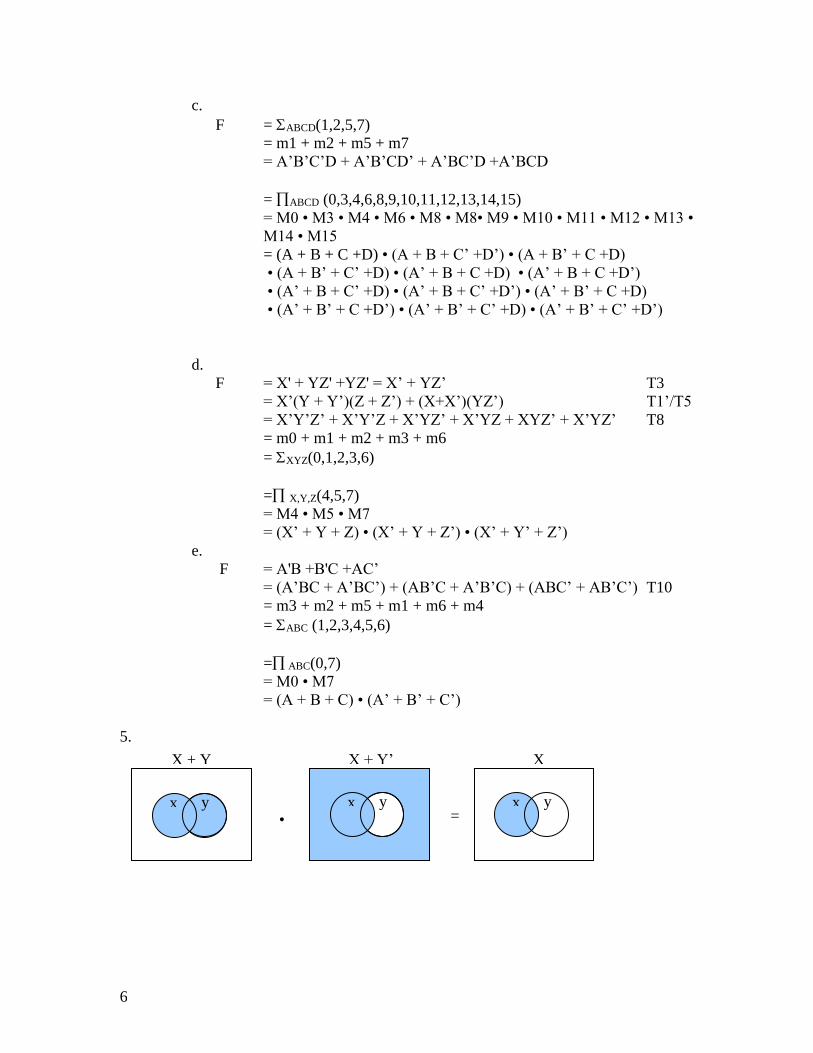
6
c
F = ABCD(1257)
= m1 + m2 + m5 + m7
= ArsquoBrsquoCrsquoD + ArsquoBrsquoCDrsquo + ArsquoBCrsquoD +ArsquoBCD
= ABCD (034689101112131415)
= M0 bull M3 bull M4 bull M6 bull M8 bull M8bull M9 bull M10 bull M11 bull M12 bull M13 bull
M14 bull M15
= (A + B + C +D) bull (A + B + Crsquo +Drsquo) bull (A + Brsquo + C +D)
bull (A + Brsquo + Crsquo +D) bull (Arsquo + B + C +D) bull (Arsquo + B + C +Drsquo)
bull (Arsquo + B + Crsquo +D) bull (Arsquo + B + Crsquo +Drsquo) bull (Arsquo + Brsquo + C +D)
bull (Arsquo + Brsquo + C +Drsquo) bull (Arsquo + Brsquo + Crsquo +D) bull (Arsquo + Brsquo + Crsquo +Drsquo)
d
F = X + YZ +YZ = Xrsquo + YZrsquo T3
= Xrsquo(Y + Yrsquo)(Z + Zrsquo) + (X+Xrsquo)(YZrsquo) T1rsquoT5
= XrsquoYrsquoZrsquo + XrsquoYrsquoZ + XrsquoYZrsquo + XrsquoYZ + XYZrsquo + XrsquoYZrsquo T8
= m0 + m1 + m2 + m3 + m6
= XYZ(01236)
= XYZ(457)
= M4 bull M5 bull M7
= (Xrsquo + Y + Z) bull (Xrsquo + Y + Zrsquo) bull (Xrsquo + Yrsquo + Zrsquo)
e
F = AB +BC +ACrsquo
= (ArsquoBC + ArsquoBCrsquo) + (ABrsquoC + ArsquoBrsquoC) + (ABCrsquo + ABrsquoCrsquo) T10
= m3 + m2 + m5 + m1 + m6 + m4
= ABC (123456)
= ABC(07)
= M0 bull M7
= (A + B + C) bull (Arsquo + Brsquo + Crsquo)
5
X + Y X + Yrsquo X
= bull x y x y x y
7
6 One possible solution
XY + XrsquoZ + YZ
XY + XrsquoZ + YZ bull 1 T1rsquo
XY + XrsquoZ + YZ bull (X + Xrsquo) T5
XY + XrsquoZ + XYZ + XYZ T8
(XY + XYZ) + (XrsquoZ + XrsquoZY) T6
XY + XrsquoZ T9
7
a
F = XrsquoZrsquo + (Y(Xrsquo+Z))rsquo
= XrsquoZrsquo + Yrsquo + (Xrsquo+Z)rsquo DEMORGANS
= XrsquoZrsquo + Yrsquo + XZrsquo DEMORGANS
= (Xrsquo + X) bull Zrsquo + Yrsquo T8
= 1 bull Zrsquo + Yrsquo T5
POS = Zrsquo + Yrsquo T1rsquo
b
G = XY + YrsquoZrsquo
= (XY + Yrsquo)(XY + Zrsquo) T8rsquo
= (X + Yrsquo)(Y + Yrsquo)(X + Zrsquo)(Y + Zrsquo) T8rsquo
= (X + Yrsquo)(X + Zrsquo)(Y + Zrsquo) T3rsquo
= (X + Yrsquo)(Y + Zrsquo) T11rsquo
POS = (X + Yrsquo) bull (Y + Zrsquo)
c
H = AB bull (CD)rsquo + A + D
= (AB bull (Crsquo + Drsquo)) + A + D DEMORGANS
= (AB + A + D) bull (Crsquo + Drsquo + A + D) T8rsquo
= (A(B+1) + D) bull (1)
= (A + D) bull 1 T1rsquo
POS = A + D
8
Z = AB + (Crsquo + ArsquoBrsquo)rsquo + Arsquo(AB + ACrsquoDrsquo)
= AB + (Crsquo + ArsquoBrsquo)rsquo + ArsquoAB + ArsquoACrsquoDrsquo T8
= AB + Cbull (A+B) + 0 + 0 DEMORGANS T5rsquo
SOP = AB + AC + BC T8
9
a F = xrsquoyrsquo + xyrsquoz + zrsquo
Let us simplify first
= yrsquo(xrsquo + xz) + zrsquo
= yrsquo(xrsquo(z + zrsquo) + xz) + zrsquo T1rsquo T5
= yrsquo(xrsquoz + xrsquozrsquo + xz) + zrsquo T8
8
= yrsquo(xrsquoz + xrsquoz + xrsquozrsquo + xz) + zrsquo T3 (replicate terms)
= yrsquo(xrsquo(z+zrsquo) + z(xrsquo+x)) + zrsquo T8
= yrsquo(xrsquo +z) + zrsquo T5T1rsquo
Now let us convert to POS using T8rsquo
= (zrsquo+yrsquo)(zrsquo + xrsquo + z) T8rsquo
= (zrsquo+yrsquo) T5T1rsquo
b G = (xrsquo+yrsquo)(y)(wrsquo+y+z)
Convert to SOP using T8 (simplifying as we go)
= (xrsquoy + yrsquoy)(wrsquo + y + z) T8
= xrsquoy(wrsquo + y + z) T5rsquoT1
= wrsquoxrsquoy + xrsquoy + xrsquoyz T8
= xrsquoy(wrsquo + 1 + z) T8
= xrsquoy T2 T1rsquo
9
HW4 - Circuit Design w Karnaugh Maps
1
a F = ABCD(12459101213)
FSOP = CD BC BCD+ +
b F = MNOP(01289)
FSOP = N OP MO+ +
c F = ABCD (01258101115)
1
1
0
1 1
1 1 1 1
3
12 8
9 13 5 1
00 01 11 10
00
01
2 6
7 15
14 10
11
4
11
10
AB
CD
1
1
1
1
1 0
1
1 1
3
12 8
9 13 5 1
00 01 11 10
00
01
2 6
7 15
14 10
11
4
11
10
AB
CD
1
1
1
1
1
1
1
0
1 1
1 1
3
12 8
9 13 5 1
00 01 11 10
00
01
2 6
7 15
14 10
11
4
11
10
MN
OP
10
FSOP = ACD ACD BD+ +
d F = WXYZ (3671214)
FSOP = WY WZ X Z+ +
2
a F = XrsquoYrsquo + XrsquoZrsquo + WrsquoX + XYZ
FPOS = (Wrsquo + Xrsquo + Y)(X + Yrsquo + Zrsquo)(Wrsquo + Xrsquo + Z)
b The 4-bit prime numbers are 2 3 5 7 11 13
FPOS = (C+D)(Brsquo+D)(Arsquo+D)(Arsquo+B+C)
1
1
1
1
1 0
1 1
1 1 1 1
3
12 8
9 13 5 1
00 01 11 10
00
01
2 6
7 15
14 10
11
4
11
10
WX
YZ
0
1
1
1
1
0
0
1
1 0
1 0 1
1 0 1 1
3
12 8
9 13 5 1
00 01 11 10
00
01
2 6
7 15
14 10
11
4
11
10
WX
YZ
1
1
1
0
0
1
0
0 0
0 0 0
0 1 1 0
3
12 8
9 13 5 1
00 01 11 10
00
01
2 6
7 15
14 10
11
4
11
10
AB
CD
11
c The 4-bit numbers that are not perfect squares or cubes are 2 3 5 6 7
10 11 12 13 14 15
FPOS = (B + C)(A + C + D)
d The 4-bit numbers divisible by 3 or 5 are 0 3 5 6 9 10 12 15
FPOS = (A+B+C+Drsquo)(A+B+Crsquo+D)(A+Brsquo+C+D)(A+Brsquo+Crsquo+Drsquo)(Arsquo+B+C+D)bull
(Arsquo+B+Crsquo+Drsquo)(Arsquo+Brsquo+C+Drsquo)(Arsquo+Brsquo+Crsquo+D)
3 The K-Maps are below
FSOP = CD BC BCD+ +
1
1
1
1
1
1
1
1
0 0
0 1 0
0 1 1 0
3
12 8
9 13 5 1
00 01 11 10
00
01
2 6
7 15
14 10
11
4
11
10
AB
CD
1
0
0
1
1
0
0
1
1 0
0 1 0
1 0 1 0
3
12 8
9 13 5 1
00 01 11 10
00
01
2 6
7 15
14 10
11
4
11
10
AB
CD
1
1
0
1 1
1 1 1 1
3
12 8
9 13 5 1
00 01 11 10
00
01
2 6
7 15
14 10
11
4
11
10
AB
CD
12
FPOS = ( )( )( )C D B C B C D+ + + +
a AND ndash OR Implementation
B
Crsquo
D
CDrsquo
Brsquo
b OR - AND Implementation
Drsquo
Crsquo
Brsquo
CD
B
0
0
0
0
0
0
0 0
0
3
12 8
9 13 5 1
00 01 11 10
00
01
2 6
7 15
14 10
11
4
11
10
AB
CD
13
c NAND - NAND Implementation
B
Crsquo
D
CDrsquo
Brsquo
d NOR - NOR Implementation
Drsquo
Crsquo
Brsquo
CD
B
14
4
a The values with an odd number of 1s are 1 2 4 7 8 11 13 14 The
Donrsquot Care numbers are 0 4 5 8 10 12 and 15
SOP = ArsquoCrsquo + BD + AC + BrsquoDrsquo
b F = BrsquoCrsquoDrsquo + BCDrsquo + ABCrsquoD d = ArsquoBCrsquoD + ArsquoBrsquoCDrsquo
F = (A+Arsquo)BrsquoCrsquoDrsquo + (A+Arsquo)BCDrsquo + ABCrsquoD
= ABrsquoCrsquoDrsquo + ArsquoBrsquoCrsquoDrsquo + ABCDrsquo + ArsquoBCDrsquo + ABCrsquoD
d = ArsquoBCrsquoD + ArsquoBrsquoCDrsquo
FSOP = BrsquoCrsquoDrsquo + BCrsquoD + BCDrsquo
1
1
d
1
1
d
d 0
1 d 1
1 d 1
3
12 8
9 13 5 1
00 01 11 10
00
01
2 6
7 15
14 10
11
4
11
10
AB
CD
d
1
1
1 0
1
1 d
3
12 8
9 13 5 1
00 01 11 10
00
01
2 6
7 15
14 10
11
4
11
10
AB
CD
15
5
a F = ArsquoC + ACE + CABrsquo + BrsquoArsquoDE + Arsquo Drsquo Ersquo
FSOP = ArsquoC + ArsquoDrsquoErsquo + ArsquoBrsquoDE + BrsquoC + CE
b F = (AB + ArsquoBrsquo) (CrsquoDrsquo + CD)
= ABCrsquoDrsquo + ArsquoBrsquoCrsquoDrsquo + ABCD + ArsquoBrsquoCD
bull K-Map
FSOP = ABCrsquoDrsquo + ArsquoBrsquoCrsquoDrsquo + ABCD + ArsquoBrsquoCD
1
1
1 0
1
3
12 8
9 13 5 1
00 01 11 10
00
01
2 6
7 15
14 10
11
4
11
10
AB
CD
1
0
1
1
1
1
0
0
1 0
1 1 1
0 1 1
3
12 8
9 13 5 1
00 01 11 10
00
01
2 6
7 15
14 10
11
4
11
10
BC
DE
0
0
1
1
1
0
0
0
0 0
1 0 0
0 1 1 0
3
12 8
9 13 5 1
00 01 11 10
00
01
2 6
7 15
14 10
11
4
11
10
BC
DE
A=0 A=1
16
bull NAND ndash NAND Implementation
B
Crsquo
Drsquo
D
C
A
Arsquo
Brsquo
c F = ArsquoBrsquoCrsquoDrsquo + ArsquoBrsquoCDrsquo + ArsquoBCrsquoDrsquo + ArsquoBCrsquoD + ABrsquoCDrsquo
bull K-Map
FSOP = ArsquoCrsquoDrsquo + ArsquoBCrsquo + BrsquoCDrsquo
bull NAND ndash NAND Implementation
ArsquoCrsquo
Drsquo
B
Brsquo
C
1
1
1 0
1
1
3
12 8
9 13 5 1
00 01 11 10
00
01
2 6
7 15
14 10
11
4
11
10
AB
CD
F
F
17
d The numbers are 2 3 4 5 10 12 13 14 15
bull K-Map
SOP = AB + BCrsquo + ArsquoBrsquoC + ACDrsquo
bull NAND ndash NAND Implementation
A
B
Crsquo
ArsquoBrsquoC
Drsquo
1
1
1
1
1
0
1 1
1 1
3
12 8
9 13 5 1
00 01 11 10
00
01
2 6
7 15
14 10
11
4
11
10
AB
CD
18
6
a F = ArsquoC + ACE + CABrsquo + BrsquoArsquoDE + Arsquo Drsquo Ersquo
bull K-Map
FPOS = (Arsquo + Crsquo)(Arsquo + Brsquo + E)(Brsquo+C+Ersquo)(C + D + Ersquo)(C + Drsquo + E)
b F = (AB + ArsquoBrsquo) (CrsquoDrsquo + CD)
bull K-Map
FPOS = (A + Brsquo)(Arsquo + B)(C + Drsquo)(Crsquo + D)
0
0
0
0
0
0
0
0 0
0 0 0 0
3
12 8
9 13 5 1
00 01 11 10
00
01
2 6
7 15
14 10
11
4
11
10
AB
CD
1
0
1
1
1
1
0
0
1 0
1 1 1
0 1 1 0
3
12 8
9 13 5 1
00 01 11 10
00
01
2 6
7 15
14 10
11
4
11
10
BC
DE
0
0
1
1
1
0
0
0
0 0
1 0 0
0 1 1 0
3
12 8
9 13 5 1
00 01 11 10
00
01
2 6
7 15
14 10
11
4
11
10
BC
DE
A=0 A=1
19
NOR ndash NOR Implementation
A
Brsquo
Arsquo
B
CDrsquo
Crsquo
D
c F = ArsquoBrsquoCrsquoDrsquo + ArsquoBrsquoCDrsquo + ArsquoBCrsquoDrsquo + ArsquoBCrsquoD + ABrsquoCDrsquo
bull K-Map
FPOS = (B + Drsquo)(Brsquo + Crsquo)(Arsquo + C)
bull NOR ndash NOR Implementation
B
Drsquo
BrsquoCrsquo
ArsquoC
0
0
0
0
0
0
0
0 0
0 0 0
3
12 8
9 13 5 1
00 01 11 10
00
01
2 6
7 15
14 10
11
4
11
10
AB
CD
F
F
20
d The numbers are 2 3 4 5 10 12 13 14 15
bull K-Map
POS = (B + C)(A + Brsquo + Crsquo)(Arsquo + B + Drsquo)
bull NOR ndash NOR Implementation
BC
ABrsquoCrsquo
Arsquo
Drsquo
7 A and B are both 2-bit signed numbers They range from -2 to +1 Thus F = A + B
is ranging from -4 to +2 We need 3 bits to represent the signed number F
a The block diagram is below
A1
A0
B1
B0
F2
F1
F0
0
0
0
0 0
0
0 0
3
12 8
9 13 5 1
00 01 11 10
00
01
2 6
7 15
14 10
11
4
11
10
AB
CD
F
21
b The truth table is below
A1 A0 B1 B0 F2 F1 F0
0 0 0 0 0 0 0
0 0 0 1 0 0 1
0 0 1 0 1 1 0
0 0 1 1 1 1 1
0 1 0 0 0 0 1
0 1 0 1 0 1 0
0 1 1 0 1 1 1
0 1 1 1 0 0 0
1 0 0 0 1 1 0
1 0 0 1 1 1 1
1 0 1 0 1 0 0
1 0 1 1 1 0 1
1 1 0 0 1 1 1
1 1 0 1 0 0 0
1 1 1 0 1 0 1
1 1 1 1 1 1 0
c
K-Map of output ldquoF2rdquo K-Map of output ldquoF1rdquo
F2SOP = A1A0rsquo + B1B0rsquo + A1B1 + A1B0rsquo + A0rsquoB1
F1SOP = A1B1rsquoB0rsquo + A1A0rsquoB1rsquo + A1rsquoA0rsquoB1 + A1rsquoB1B0rsquo + A1rsquoA0B1rsquoB0 + A1A0B1B0
1
1
1
1
1
1
1
0
1 1
1
3
12 8
9 13 5 1
00 01 11 10
00
01
2 6
7 15
14 10
11
4
11
10
A1A0
B1B0
1
1
1
1
0
1 1
1 1
3
12 8
9 13 5 1
00 01 11 10
00
01
2 6
7 15
14 10
11
4
11
10
A1A0
B1B0
22
K-Map of output ldquoF0rdquo
F0SOP = A0B0rsquo + A0rsquoB0
d AND-OR implementation
Implementation of F2
A1A0
B1
B0
Implementation of F1
The implementation consists of four 3-input AND gates two 4-input AND gates and one
6-input OR gate
Implementation of F0
A0B0
A0
B0
1
1
1
1
0
1 1
1 1
3
12 8
9 13 5 1
00 01 11 10
00
01
2 6
7 15
14 10
11
4
11
10
A1A0
B1B0
23
NAND ndash NAND Implementation
(1) Implementation of F2
A1A0
B1
B0
(2) Implementation of F1
The implementation consists of four 3-input NAND gates two 4-input NAND gates and
one 6-input NAND gate
(3) Implementation of F0
A0B0
A0
B0
24
8 X is a 3-bit unsigned number It ranges from 0 to 7 Thus Y = 3X + 1 is ranging
from 1 to 22 We need 5 bits to represent the unsigned number Y
a The block diagram is below
X2
X1
X0
Y4
Y3Y2
Y1
Y0
b The truth table is below
X X2 X1 X0 Y4 Y3 Y2 Y1 Y0 Y
0 0 0 0 0 0 0 0 1 1
1 0 0 1 0 0 1 0 0 4
2 0 1 0 0 0 1 1 1 7
3 0 1 1 0 1 0 1 0 10
4 1 0 0 0 1 1 0 1 13
5 1 0 1 1 0 0 0 0 16
6 1 1 0 1 0 0 1 1 19
7 1 1 1 1 0 1 1 0 22
c
K-Map of output ldquoY4rdquo K-Map of output ldquoY3rdquo
Y4POS = X2(X1 + X0) Y3POS = (X2 + X1)(X1rsquo + X0)(X2rsquo + X0rsquo)
K-Map of output ldquoY2rdquo
Y2POS = (X2 + X1 + X0)( X2 + X1rsquo + X0rsquo)( X2rsquo + X1rsquo + X0)( X2rsquo + X1 + X0rsquo)
0 0
0 0
0 0
6 4
5 7 3 1
00 01 11 10
0
1
2
X2X1
X0
0 0
0 0
0 0 0
6 4
5 7 3 1
00 01 11 10
0
1
2
X2X1
X0
0 0
0
0 0
6 4
5 7 3 1
00 01 11 10
0
1
2
X2X1
X0
25
K-Map of output ldquoY1rdquo K-Map of output ldquoY0rdquo
Y1POS = X1 Y0POS = X0rsquo
d
bull OR ndash AND Implementation
Implementation of Y4
X1
X0
X2
Implementation of Y3
X2
X1
X1
X0
X2
X0
0 0
0
0 0
6 4
5 7 3 1
00 01 11 10
0
1
2
X2X1
X0
0
0 0 0 0
6 4
5 7 3 1
00 01 11 10
0
1
2
X2X1
X0
26
Implementation of Y2
X2X1X0
X1
X0
X2
Implementation of Y1 (straight wire connection)
Y1X1
Implementation of Y0 (straight wire connection)
Y0X0
bull NOR ndash NOR Implementation
Convert all gates in the above implementations to NOR gates For Y1 and Y0 just use
wires
27
e This will not be covered at this point of the class since we have not yet discussed
adders Ignore this question
9 X is a 3-bit signed number It ranges from -4 to +3
Thus Z = X2 + 2X + 1 = (X + 1)2 is ranging from 0 to +16 We need 6 bits to
represent signed number Z
a The block diagram is below
Z5
Z4
Z3
Z2Z1
Z0
X0
X1
X2
b The truth table is below
X X2 X1 X0 Z5 Z4 Z3 Z2 Z1 Z0 Z
+0 0 0 0 0 0 0 0 0 1 +1
+1 0 0 1 0 0 0 1 0 0 +4
+2 0 1 0 0 0 1 0 0 1 +9
+3 0 1 1 0 1 0 0 0 0 +16
-1 1 1 1 0 0 0 0 0 0 +0
-2 1 1 0 0 0 0 0 0 0 +1
-3 1 0 1 0 0 0 0 0 0 +4
-4 1 0 0 0 0 1 0 0 1 +9
c
No K-Map needed for Z5 ldquoZ5rdquo = 0
K-Map of output ldquoZ4rdquo K-Map of output ldquoZ3rdquo
Z4SOP = X2rsquoX1X0 Z3SOP = X2rsquoX1X0rsquo + X2X1rsquoX0rsquo
0
1
6 4
5 7 3 1
00 01 11 10
0
1
2
X2X1
X0
0
1 1
6 4
5 7 3 1
00 01 11 10
0
1
2
X2X1
X0
28
K-Map of output ldquoZ2rdquo K-Map of output ldquoZ0rdquo
Z2SOP = X2rsquoX1rsquoX0 Z0SOP = X2rsquoX0rsquo + X1rsquoX0rsquo
Note Z1 = 0 (constant)
0
1
6 4
5 7 3 1
00 01 11 10
0
1
2
X2X1
X0
1 0
1 1
6 4
5 7 3 1
00 01 11 10
0
1
2
X2X1
X0
29
10 Design a 1-bit comparator that takes in a bit X and a bit Y and outputs XltY
XgtY X=Y Use a single 2-to-4 decoder and 1 single OR gate
Consider the truth table of each of these simple functions We can implement
each as a sum of minterms And since a decoder implements the minterms of
the input variables we can arrive at the circuit above
X Y XltY XgtY X==Y
0 0 0 0 1
0 1 1 0 0
1 0 0 1 0
1 1 0 0 1
Y0
Y1
Y2
Y3
A0
A1
2-t
o-4
Decoder
X
Y XltY
XgtY
X=Y
30
HW5 - Signed Representations and Arithmetic
1
a
11 1
10100 = 20
+ 11101 = 29
Carry=1 110001 = 49
b
11100
- 10100
01000
28
- 20
8
1 1 1 1 _
11100
2rsquos comp 01011
+ 1
01000
2
b
1 1 1 1 _
101011
+ 011010
1000101
3 For unsigned subtraction we still use take the 2s complement of the bottom
number (but the check for overflow differs for unsigned vs 2s complement)
a 01101102 ndash 01001002 cannot be performed as is because we cannot
subtract a larger number from a smaller number in unsigned
representation
0110110
- 0100100
+54
-60
-6
1 1 1 1 1 1 _
0110110
2rsquos comp 1011011
+ 1
0010010
4
a Unsigned binary 28 lt 28310 lt 29 Therefore 9 bits 28310 = 1000110112
b 2rsquos complement with n-bits we can make ndash(2n-1) to +(2n-1-1) With n = 9
the range is -256 to +256 With n = 10 the range is -512 to +511 Thus
10 bits 28310 = 1000110112
5 Consider the following decimal numbers +21 +55 +121 -32 -99 -128
a What are the corresponding 8-bit signed-magnitude representation
31
a What are the corresponding 8-bit 2s complement representation
b Which of the above numbers can be represented in 6-bit signed-
magnitude 6-bit 1s complement 6-bit 2s complement representations
explain
21 55 121 -32 -99 -128 A 16+4+1=21
00010101 00110111 01111001 10100000 11100011 NA
B 00010101 00110111 01111001 1110000 10011101 10000000 C YYY
010101 in all cases
NNN NNN NNY 100000 in 2rsquos comp
NNN NNN
6 What are the corresponding decimal representations for the following binary
numbers 01011011 11010010 if
a The binary numbers are in 8-bit signed-magnitude format
b The binary numbers are in 8-bit 2s complement format
01011011 11010010 a) 64+16+8+2+1=91 -(64+16+2)=-82 b) 64+16+8+2+1=91 -128+64+16+2=-46
7 Perform the following addition problems for the following 2rsquos complement
numbers State whether overflow does or does not occur for each problem
Justify your answer for why overflow does or does not occur Check your
work by converting each number to decimal
a 1010 0111 b 1001 0110 c 0101 1100 d 0101 1101
+1110 0100 +1011 0011 +1011 0101 +0110 1001
11000 1011 10100 1001 10001 0001 1100 0110
n+n=n
cin=cout=1
No Overflow
n+n=p
cin=0cout=1
Overflow
p+n=p
cin=cout=1
NoOverflow
p+p=n
cin=1cout=0
Overflow
8 This is an exercise to help you remember what gates are used to create a full
adder Using a full adder as shown below and no other gates can you
produce the function Z = AbullB (Hint Write out the logical equations for S
and Cout and see if you can hook up the inputs to produce Z)
ANSWER
Cin X Y S Cout
0 0 0 0 0
32
0 0 1 1 0
0 1 0 1 0
0 1 1 0 1
1 0 0 1 0
1 0 1 0 1
1 1 0 0 1
1 1 1 1 1
S X Y Cin
Cout XY XCin YCin
=
= + +
We want Z=XY and if we set Cin=0 then the formulas of S and Cout
becomes as follows
S X Y
Cout XY
=
=
Thus Cout = Z = XY
X Y
S
CinFull Adder
Cout
A B
0Z
33
9 Using 1 half-adder and a minimal number of 4-bit binary adders design a
circuit to calculate Y = 25X where X is a 4-bit inputs
ANSWER
If a number is multiplied by a number that is a power of 2 then the number rewritten
using the above formula
2 00
n
n X X=
Y = 25X = 16X + 8X + X = X0000+X000+X
Also adding the information that X is a 4-bit number above formula can be re-written
X = X3X2X1X0
Y = X3X2X1X00000 + X3X2X1X0000 + X3X2X1X0
This can be written as addition by 4 bit adders
X3 X2 X1 X0
X3 X2 X1 X0 0 0 0
+ X3 X2 X1 X0 0 0 0 0
Since one row in each addition is all zeros they can be eliminated and the other two
numbers can be added using a 4-bit adder However the lower bits require only a single
bit adder The carry from the first addition is transferred to the next one
B3 B2 B1 B0 A3 A2 A1 A0
S0S1S2S3
C0C4 4-bit Binary Adder
X Y
S
Half AdderCout
X3 X0X0X1X2X3 X1X2X30 X0X1X2
Y8 Y7 Y6 Y5 Y4 Y3 Y0Y1Y2
34
10 Using a minimal number of 4-bit adders design a circuit that implements
Y=20X+107 where X is a 3-bit unsigned number
ANSWER
X = X2X1X0 and thus 20X= 16X+4X These numbers are achieved by inserting zeros
at the end Once we add these there numbers we see that not all bits require addition We
actually need only a single 4-bit adder and nothing more
1 1 0 1 0 1 1
X2 X1 X0 0 0
+ X2 X1 X0 0 0 0 0
Which can be collapsed to the following addition
1 1 X2 X1 X0 0 0
+ X2 X1 X0 1 0 1 1
B3 B2 B1 B0 A3 A2 A1 A0
S0S1S2S3
C0C4 4-bit Binary Adder
X0X1X2 X1X211
11
X0
Y7 Y6 Y5 Y4 Y3 Y0Y1Y2
0
1
35
11 Design a minimal circuit using ANDORNOT gates to implement the
comparison A gt 10 where A is a 4-bit number
a Start by writing out the logical algorithm for when A gt 10 then implement it
using gates
b Check that your work is minimal by using a K-Map
ANSWER
Letrsquos assume that the number A = A3A2A1A0
Logical Algorithm For any number A to be greater than a number B (in this case 1010 =
10102) a more significant bit of A must be greater than B However in the case of A
compared with 1010 we realize A3 and A1 can never be greater than the 1rsquos in those
places for 10 Similarly A2 and A0 can never be less than the 0rsquos in those places Thus
for A gt 10 there are only 2 cases that need to be checked
A3 = 1 and A2 gt 0 (ie A2 = 1)
OR
A3=1 and A1 = 1 and A0 gt 0 (ie A0 = 1)
Thus Agt10 = A3A2 + A3A2A0
Note that we donrsquot have to check A2 in the second case because it is DEFINITELY
greater than or equal to the 0 in that place of 10102
A K-Map will also show the same equation
SUM(1112131415)
Agt10=A3A2+ A3A1A0
A3
A2
A3
A0A1
Agt10
1
1
1
0
1
1
3
12 8
9 13 5 1
00 01 11 10
00
01
2 6
7 15
14 10
11
4
11
10
A3A2
A1A0
36
HW 6 ndash Latches and Flip-Flops
1 Complete the following waveforms for negative edge-triggered D Flip-Flops
D Q
QCK
D Q
QCK
CLK
D1
D2D1
D2
Z
X
CLK
X
D1
D2
Z
2 We should find the state diagram following the steps in the class notes
a Convert the diagram to a table
Current
State
Next State Output
XY= 00 XY= 01 XY= 10 XY= 11
Q1 Q0 Q1 Q0
Q1
Q0 Q1
Q0 Q1
Q0 Z
0 0 0 0 0 0 1 0 1 0 0
0 1 0 0 0 0 0 1 0 1 1
1 0 0 0 0 1 0 0 0 1 0
1 1 0 0 0 1 0 1 0 1 0
37
Convert Q to D
Current
State
Next State Output
XY= 00 XY= 01 XY= 10 XY= 11
Q1 Q0 D1 D0 D1 D0 D1 D0 D1 D0 Z
0 0 0 0 0 0 1 0 1 0 0
0 1 0 0 0 0 0 1 0 1 1
1 0 0 0 0 1 0 0 0 1 0
1 1 0 0 0 1 0 1 0 1 0
b Perform K-maps to find equations for D1 and D0
D0 = Q1Y + Q0X
D1 = Q1rsquoQ0rsquoX
c Draw the circuit and implement the initial state (reset) condition
D Q
QCK
D Q
QCK
ZX
Clock
Q0
Q1Y
PRE PRE
CLR CLR
Reset Reset
GND GND
38
3 Because we have 2 states in the state diagram we use one D flip-flop to
implement state memory We design the combinational logic for the next-state
logic and the output function logic by building up the statetransition table
Current State Next State Output
XY = 00 XY = 01 XY = 10 XY = 11
SymbolCode SymbolCode SymbolCode SymbolCode SymbolCode H
F 0 F 0 G 1 G 1 G 1 0
G 1 F 0 F 0 F 0 G 1 1 Q0(t) Q0
D0 Q0
D0 Q0
D0 Q0
D0
After we get the statetransition table we build the K-Maps to simplify expressions for
D0 and H
bull D0 K-Map
D0 = YQ0rsquo + XQ0rsquo + XY H = Q0
0
1 1 1
1
6 4
5 7 3 1
00 01 11 10
0
1
2
XY
Q0
39
4
Current State Next State amp Flop-Flop Inputs Outputs
Next State Next State
X = 0 X = 1
SymbolCode SymbolCode SymbolCode Z
A00 B01 D11 0
B01 C10 B01 0
C10 B01 A00 1
D11 B01 C10 0 Q1(t)Q0(t) Q1(t+1)Q0(t+1) Q1(t+1)Q0(t+1)
After we get the statetransition table we build the K-Maps to simplify expressions for
D1 D0 and Z
bull D1 K-Map D0 K-Map
D1 = XrsquoQ1Q0 + XQ0rsquo D0 = XrsquoQ1+XQ0 + XQ1rsquo
Z K-Map
Z = Q1Q0rsquo
1
1 0
0 1
1 0
1 00
01
11
10
0 Q1Q0
X
1
1
0 0
1 0
0 1
0 00
01
11
10
0 Q1Q0
X
1
1
0 0
0 0
1
0 Q0
Q1
1
40
a The waveform is below
CLK
X
Q1
Q0
State
Z
A D B C A B
41
5
a We need 4 states and each of them stores one 2-bit binary number ranging
from 00 to 11
State S0 S1 S2 S3
Assignment
(Q1 Q0)
00 01 10 11
The state diagram is below
b Because we have 4 states in the state diagram we use two D flip-flops to
implement state memory We design the combinational logic for the next-
state logic and the output function logic by building up the statetransition
table
U ndash UP D ndash DOWN
Current State Next State
UD = 00 UD = 01 UD = 10 UD = 11
SymbolCode SymbolCode SymbolCode SymbolCode SymbolCode
S000 S000 S311 S101 S000
S101 S101 S000 S210 S101
S210 S210 S101 S311 S210
S311 S311 S210 S000 S311 Q1(t)Q0(t) Q1(t+1)Q0(t+1)
D1D0 Q1(t+1)Q0(t+1)
D1D0 Q1(t+1)Q0(t+1)
D1D0 Q1(t+1)Q0(t+1)
D1D0
After we get the statetransition table we build the K-Maps to simplify expressions for
D1 and D0
S0 S1 S2 S3
UP=DOWN=1 or
UP=DOWN=0
UP=DOWN=1 or
UP=DOWN=0
UP=DOWN=1 or
UP=DOWN=0UP=DOWN=1 or
UP=DOWN=0
UP=1 and
DOWN=0
UP=1 and
DOWN=0UP=1 and
DOWN=0
UP=1 and DOWN=0
UP=0 and
DOWN=1UP=0 and
DOWN=1
UP=0 and
DOWN=1
UP=0 and DOWN=1
~R
ese
t
42
bull D1 K-Map
D1 = UrsquoDrsquoQ1 + DQ1Q0 + UQ1Q0rsquo + UrsquoDQ1rsquoQ0rsquo + UDrsquoQ1rsquoQ0
bull D0 K-Map
D0 = UrsquoDrsquoQ0 + UDQ0 + UrsquoDQ0rsquo + UDrsquoQ0rsquo
c The waveform is below
CLK
UP
DOWN
Q1
Q0
1
1
1
1
1
1
0
1
1
3
12 8
9 13 5 1
00 01 11 10
00
01
2 6
7 15
14 10
11
4
11
10
UD
Q1Q0
1
1
1
1
0
1 1
1 1
3
12 8
9 13 5 1
00 01 11 10
00
01
2 6
7 15
14 10
11
4
11
10
UD
Q1Q0
43
6 Complete the waveform for the 4-bit counter presented in class
1111
Clock
SR
CEP
CET
PE
P3-P0
Q3-Q0 1101
1101
1110 0000 0001 0000 1110 1111
7 Complete the waveform for a 4-bit D-Register with Data (Load) Enable and
asynchronous reset
CLK
AR
EN
0110D[30] 0001 10111010 11011001 10001111 0111
Q[30] 1010 11111101 10000000 1011
44
81 Unit 7 ndash Datapath Design 1 Implement a circuit that takes in a 4-bit number X[30] and produces a 4-bit value
Z[30] according to the following function
if X lt 8 then
Z = X + 5
else
Z = X ndash 2
Using the building blocks below and at most 1 inverter (no other gates)
implement this function
Note To check Xlt8 subtract X-8 by taking the 2rsquos complement of 8 The 2rsquos comp of
8 is 0111+1 Recall a carry of 0 when subtracting unsigned numbers (A-B) indicates
overflow which can only occur in unsigned subtraction if the result needed to be negative
(ie A lt B) So C4 will only be 1 if X is not less-than 8 We can invert it to get a signal
that is true when X lt 8 Use those signals to either add 5 (0101) or subtract 2 (add 1110)
B3 B2 B1 B0 A3 A2 A1 A0
S0S1S2S3
C0C4 4-bit Binary Adder
X lt 8
Xlt8
X0X1X2X3
Z0Z1Z2Z3
B3
B2
B1
B0
A3
A2
A1
A0
S0
S1
S2
S3
C0
C4
4-b
it B
inary
Add
er
X3
X2
X1
X0
1
1
1
0
1
0
1
45
2 Design a circuit that takes in an 4-bit number X[30] and outputs a number Y and
performs the operation below Assume these numbers are unsigned Use a 4-bit
adder and 2-to-1 muxes Hint Multiplying by 4 (ie 22) in binary can be done with
no gates just as multiplying by 100 (ie 102) in decimal can be done simply and
easily
if(X lt 00112)
Y = 4X
else
Y = X
4X would require 6 outputs and be X3 X2 X1 X0 0 0 thus even if we pass X we need to
produce 6 outputs Recall subtracting 3=0011 bin is the same as adding the 2s
complement Next a carry of 0 when subtracting unsigned numbers (A-B) indicates
overflow which can only occur in unsigned subtraction if the result needed to be negative
(ie A lt B)
I1
Y
S
I0
I1
Y
S
I0
I1
Y
S
I0
I1
Y
S
I0
I1
Y
S
I0
I1
Y
S
I0
X0
X1
X2
X3
0
0
0
0
X0
X1
X2
X3
Y5
Y4
Y3
Y2
Y0
Y1
X lt 3
B3
B2
B1
B0
A3
A2
A1
A0
S0
S1
S2
S3
C0
C4
4-b
it B
inary
Add
er
X3
X2
X1
X0
0
0
1
1
1
46
3 Design a circuit that takes in two 4-bit numbers X[30] and Y[30] along with two
function select bits FS1 and FS0 and produces an output Z[30] according to the
following table
FS1FS0 Z
00 X+Y
01 X-Y
10 Y-X
11 donrsquot care
Use (1) 4-bit adder 4-bit wide 2-to-1 muxes and any basic gates you desire
Approach Take a 4-bit adder and for each operation listed in the table above
identify what should be passed to the A and B inputs of the adder Then use
muxes to perform that function Design logic for the select bits of the muxes and
the carry-in of the adder that use FS1 and FS0 as input
Note In the solution below the A and B inputs of the muxes are like the 0th and
1st inputs of 4 2-to-1 muxes respectively Ignore the G input
B3
B2
B1
B0
A3
A2
A1
A0
S3
S2
S1
S0
C0
C4
S
G
1A
1Y
2Y
2-to-1
4-bit
wide
mux
2A
3A
4A3Y
4Y1B
2B
3B
4B
0
S
G
1A
1Y
2Y
2-to-1
4-bit
wide
mux
2A
3A
4A3Y
4Y1B
2B
3B
4B
0
X3
X2
X1
X0
X3
X2
X1
X0
Y3
Y2
Y1
Y0
Y3
Y2
Y1
Y0
Z3
Z2
Z1
Z0
FS1
FS0
FS1FS0
74LS
283
47
4 Design a circuit that takes in two 4-bit signed magnitude numbers X[30] and
Y[30] and produces two 4-bit outputs A[30] and B[30] according to the following
algorithm
if X gt= Y then
A = X and B = Y
else
A = Y and B = X
Use a 4-bit adder to subtract and perform the comparison 4-bit wide 2-to-1
muxes and basic logic gates Assume the input 1000 = -0 will never occur on X
or Y
Approach First think about how to compare signed magnitude numbers by using
unsigned comparison techniques and how to precondition the inputs to allow the
use of unsigned comparison For example 1001 = -1 in signed magnitude and
0100 = +4 in signed magnitude So 1001 is really less than 0100 Use the
comparison result to control the selects of the muxes
Y0
Y1
Y2
Y3
X0
X1
X2
X3
XgtY
S
G
1A
1Y
2Y
2-to-1
4-bit
wide
mux
2A
3A
4A3Y
4Y1B
2B
3B
4B
0
S
G
1A
1Y
2Y
2-to-1
4-bit
wide
mux
2A
3A
4A3Y
4Y1B
2B
3B
4B
0
X3
X2
X1
X0
Y3
Y2
Y1
Y0
X3
X2
X1
X0
Y3
Y2
Y1
Y0
A3
A2
A1
A0
B3
B2
B1
B0
B3
B2
B1
B0
A3
A2
A1
A0
S0
S1
S2
S3
C0
C4
4-b
it B
inary
Add
er
1
48
5 Design a circuit that adds two 4-bit unsigned numbers X[30] and Y[30] and
outputs either the sum if there is no overflow or 1111 (=1510 the maximum unsigned
4-bit number) if there is overflow
Unsigned overflow is found by looking at Cout You could use a mux to select the sum
or 1111 but realize you can just use OR gates for this function
B3
B2
B1
B0
A3
A2
A1
A0
S3
S2
S1
S0
C0
C4
74LS
283
X3
X2
X1
X0
UNS_OV
0
Y3
Y2
Y1
Y0
G0
G1
G2
G3
49
1 We would like to build an adder whose inputs are in units of pennies and produces
sum in nickels and pennies Essentially this is a base-5 adder The 2 inputs of this
adder are A=A2A1A0 and B=B2B1B0 Assume that the maximum input number
that A and B can be is 4 pennies Design an adder to produce the correct
nickelspennies sum C= [CN] [CP2CP1CP0] To implement this design you may
assume you can use as many 4-bit adders as you like
if X+Y gt 4 dec then
CN = 1 CP[20] = X+Y-5
else
CN = 0 CP[20] = X+Y
A2 A1 A0 B2 B1 B0
CP2 CP1 CP0
To be designed by you
CN
Block diagram for the
nickelpenny adder you
are going to design
50
B3 B2 B1 B0 A3 A2 A1 A0
S0S1S2S3
C0C4 4-bit Binary Adder
Z4 Z2 Z1
CP2
0
0
B3 B2 B1 B0 A3 A2 A1 A0
S0S1S2S3
C0C4 4-bit Binary Adder
0 X4 X2 X1 0 Y4 Y2 Y1
Z8 Z4 Z2 Z1
0
B3 B2 B1 B0 A3 A2 A1 A0
S0S1S2S3
C0C4 4-bit Binary Adder
0 1 0 0 Z8 Z4 Z2 Z1
1
Need actual
inverters here
just didn t
draw them
CN
(4 lt X+Y)
CP1 CP0

7
6 One possible solution
XY + XrsquoZ + YZ
XY + XrsquoZ + YZ bull 1 T1rsquo
XY + XrsquoZ + YZ bull (X + Xrsquo) T5
XY + XrsquoZ + XYZ + XYZ T8
(XY + XYZ) + (XrsquoZ + XrsquoZY) T6
XY + XrsquoZ T9
7
a
F = XrsquoZrsquo + (Y(Xrsquo+Z))rsquo
= XrsquoZrsquo + Yrsquo + (Xrsquo+Z)rsquo DEMORGANS
= XrsquoZrsquo + Yrsquo + XZrsquo DEMORGANS
= (Xrsquo + X) bull Zrsquo + Yrsquo T8
= 1 bull Zrsquo + Yrsquo T5
POS = Zrsquo + Yrsquo T1rsquo
b
G = XY + YrsquoZrsquo
= (XY + Yrsquo)(XY + Zrsquo) T8rsquo
= (X + Yrsquo)(Y + Yrsquo)(X + Zrsquo)(Y + Zrsquo) T8rsquo
= (X + Yrsquo)(X + Zrsquo)(Y + Zrsquo) T3rsquo
= (X + Yrsquo)(Y + Zrsquo) T11rsquo
POS = (X + Yrsquo) bull (Y + Zrsquo)
c
H = AB bull (CD)rsquo + A + D
= (AB bull (Crsquo + Drsquo)) + A + D DEMORGANS
= (AB + A + D) bull (Crsquo + Drsquo + A + D) T8rsquo
= (A(B+1) + D) bull (1)
= (A + D) bull 1 T1rsquo
POS = A + D
8
Z = AB + (Crsquo + ArsquoBrsquo)rsquo + Arsquo(AB + ACrsquoDrsquo)
= AB + (Crsquo + ArsquoBrsquo)rsquo + ArsquoAB + ArsquoACrsquoDrsquo T8
= AB + Cbull (A+B) + 0 + 0 DEMORGANS T5rsquo
SOP = AB + AC + BC T8
9
a F = xrsquoyrsquo + xyrsquoz + zrsquo
Let us simplify first
= yrsquo(xrsquo + xz) + zrsquo
= yrsquo(xrsquo(z + zrsquo) + xz) + zrsquo T1rsquo T5
= yrsquo(xrsquoz + xrsquozrsquo + xz) + zrsquo T8
8
= yrsquo(xrsquoz + xrsquoz + xrsquozrsquo + xz) + zrsquo T3 (replicate terms)
= yrsquo(xrsquo(z+zrsquo) + z(xrsquo+x)) + zrsquo T8
= yrsquo(xrsquo +z) + zrsquo T5T1rsquo
Now let us convert to POS using T8rsquo
= (zrsquo+yrsquo)(zrsquo + xrsquo + z) T8rsquo
= (zrsquo+yrsquo) T5T1rsquo
b G = (xrsquo+yrsquo)(y)(wrsquo+y+z)
Convert to SOP using T8 (simplifying as we go)
= (xrsquoy + yrsquoy)(wrsquo + y + z) T8
= xrsquoy(wrsquo + y + z) T5rsquoT1
= wrsquoxrsquoy + xrsquoy + xrsquoyz T8
= xrsquoy(wrsquo + 1 + z) T8
= xrsquoy T2 T1rsquo
9
HW4 - Circuit Design w Karnaugh Maps
1
a F = ABCD(12459101213)
FSOP = CD BC BCD+ +
b F = MNOP(01289)
FSOP = N OP MO+ +
c F = ABCD (01258101115)
1
1
0
1 1
1 1 1 1
3
12 8
9 13 5 1
00 01 11 10
00
01
2 6
7 15
14 10
11
4
11
10
AB
CD
1
1
1
1
1 0
1
1 1
3
12 8
9 13 5 1
00 01 11 10
00
01
2 6
7 15
14 10
11
4
11
10
AB
CD
1
1
1
1
1
1
1
0
1 1
1 1
3
12 8
9 13 5 1
00 01 11 10
00
01
2 6
7 15
14 10
11
4
11
10
MN
OP
10
FSOP = ACD ACD BD+ +
d F = WXYZ (3671214)
FSOP = WY WZ X Z+ +
2
a F = XrsquoYrsquo + XrsquoZrsquo + WrsquoX + XYZ
FPOS = (Wrsquo + Xrsquo + Y)(X + Yrsquo + Zrsquo)(Wrsquo + Xrsquo + Z)
b The 4-bit prime numbers are 2 3 5 7 11 13
FPOS = (C+D)(Brsquo+D)(Arsquo+D)(Arsquo+B+C)
1
1
1
1
1 0
1 1
1 1 1 1
3
12 8
9 13 5 1
00 01 11 10
00
01
2 6
7 15
14 10
11
4
11
10
WX
YZ
0
1
1
1
1
0
0
1
1 0
1 0 1
1 0 1 1
3
12 8
9 13 5 1
00 01 11 10
00
01
2 6
7 15
14 10
11
4
11
10
WX
YZ
1
1
1
0
0
1
0
0 0
0 0 0
0 1 1 0
3
12 8
9 13 5 1
00 01 11 10
00
01
2 6
7 15
14 10
11
4
11
10
AB
CD
11
c The 4-bit numbers that are not perfect squares or cubes are 2 3 5 6 7
10 11 12 13 14 15
FPOS = (B + C)(A + C + D)
d The 4-bit numbers divisible by 3 or 5 are 0 3 5 6 9 10 12 15
FPOS = (A+B+C+Drsquo)(A+B+Crsquo+D)(A+Brsquo+C+D)(A+Brsquo+Crsquo+Drsquo)(Arsquo+B+C+D)bull
(Arsquo+B+Crsquo+Drsquo)(Arsquo+Brsquo+C+Drsquo)(Arsquo+Brsquo+Crsquo+D)
3 The K-Maps are below
FSOP = CD BC BCD+ +
1
1
1
1
1
1
1
1
0 0
0 1 0
0 1 1 0
3
12 8
9 13 5 1
00 01 11 10
00
01
2 6
7 15
14 10
11
4
11
10
AB
CD
1
0
0
1
1
0
0
1
1 0
0 1 0
1 0 1 0
3
12 8
9 13 5 1
00 01 11 10
00
01
2 6
7 15
14 10
11
4
11
10
AB
CD
1
1
0
1 1
1 1 1 1
3
12 8
9 13 5 1
00 01 11 10
00
01
2 6
7 15
14 10
11
4
11
10
AB
CD
12
FPOS = ( )( )( )C D B C B C D+ + + +
a AND ndash OR Implementation
B
Crsquo
D
CDrsquo
Brsquo
b OR - AND Implementation
Drsquo
Crsquo
Brsquo
CD
B
0
0
0
0
0
0
0 0
0
3
12 8
9 13 5 1
00 01 11 10
00
01
2 6
7 15
14 10
11
4
11
10
AB
CD
13
c NAND - NAND Implementation
B
Crsquo
D
CDrsquo
Brsquo
d NOR - NOR Implementation
Drsquo
Crsquo
Brsquo
CD
B
14
4
a The values with an odd number of 1s are 1 2 4 7 8 11 13 14 The
Donrsquot Care numbers are 0 4 5 8 10 12 and 15
SOP = ArsquoCrsquo + BD + AC + BrsquoDrsquo
b F = BrsquoCrsquoDrsquo + BCDrsquo + ABCrsquoD d = ArsquoBCrsquoD + ArsquoBrsquoCDrsquo
F = (A+Arsquo)BrsquoCrsquoDrsquo + (A+Arsquo)BCDrsquo + ABCrsquoD
= ABrsquoCrsquoDrsquo + ArsquoBrsquoCrsquoDrsquo + ABCDrsquo + ArsquoBCDrsquo + ABCrsquoD
d = ArsquoBCrsquoD + ArsquoBrsquoCDrsquo
FSOP = BrsquoCrsquoDrsquo + BCrsquoD + BCDrsquo
1
1
d
1
1
d
d 0
1 d 1
1 d 1
3
12 8
9 13 5 1
00 01 11 10
00
01
2 6
7 15
14 10
11
4
11
10
AB
CD
d
1
1
1 0
1
1 d
3
12 8
9 13 5 1
00 01 11 10
00
01
2 6
7 15
14 10
11
4
11
10
AB
CD
15
5
a F = ArsquoC + ACE + CABrsquo + BrsquoArsquoDE + Arsquo Drsquo Ersquo
FSOP = ArsquoC + ArsquoDrsquoErsquo + ArsquoBrsquoDE + BrsquoC + CE
b F = (AB + ArsquoBrsquo) (CrsquoDrsquo + CD)
= ABCrsquoDrsquo + ArsquoBrsquoCrsquoDrsquo + ABCD + ArsquoBrsquoCD
bull K-Map
FSOP = ABCrsquoDrsquo + ArsquoBrsquoCrsquoDrsquo + ABCD + ArsquoBrsquoCD
1
1
1 0
1
3
12 8
9 13 5 1
00 01 11 10
00
01
2 6
7 15
14 10
11
4
11
10
AB
CD
1
0
1
1
1
1
0
0
1 0
1 1 1
0 1 1
3
12 8
9 13 5 1
00 01 11 10
00
01
2 6
7 15
14 10
11
4
11
10
BC
DE
0
0
1
1
1
0
0
0
0 0
1 0 0
0 1 1 0
3
12 8
9 13 5 1
00 01 11 10
00
01
2 6
7 15
14 10
11
4
11
10
BC
DE
A=0 A=1
16
bull NAND ndash NAND Implementation
B
Crsquo
Drsquo
D
C
A
Arsquo
Brsquo
c F = ArsquoBrsquoCrsquoDrsquo + ArsquoBrsquoCDrsquo + ArsquoBCrsquoDrsquo + ArsquoBCrsquoD + ABrsquoCDrsquo
bull K-Map
FSOP = ArsquoCrsquoDrsquo + ArsquoBCrsquo + BrsquoCDrsquo
bull NAND ndash NAND Implementation
ArsquoCrsquo
Drsquo
B
Brsquo
C
1
1
1 0
1
1
3
12 8
9 13 5 1
00 01 11 10
00
01
2 6
7 15
14 10
11
4
11
10
AB
CD
F
F
17
d The numbers are 2 3 4 5 10 12 13 14 15
bull K-Map
SOP = AB + BCrsquo + ArsquoBrsquoC + ACDrsquo
bull NAND ndash NAND Implementation
A
B
Crsquo
ArsquoBrsquoC
Drsquo
1
1
1
1
1
0
1 1
1 1
3
12 8
9 13 5 1
00 01 11 10
00
01
2 6
7 15
14 10
11
4
11
10
AB
CD
18
6
a F = ArsquoC + ACE + CABrsquo + BrsquoArsquoDE + Arsquo Drsquo Ersquo
bull K-Map
FPOS = (Arsquo + Crsquo)(Arsquo + Brsquo + E)(Brsquo+C+Ersquo)(C + D + Ersquo)(C + Drsquo + E)
b F = (AB + ArsquoBrsquo) (CrsquoDrsquo + CD)
bull K-Map
FPOS = (A + Brsquo)(Arsquo + B)(C + Drsquo)(Crsquo + D)
0
0
0
0
0
0
0
0 0
0 0 0 0
3
12 8
9 13 5 1
00 01 11 10
00
01
2 6
7 15
14 10
11
4
11
10
AB
CD
1
0
1
1
1
1
0
0
1 0
1 1 1
0 1 1 0
3
12 8
9 13 5 1
00 01 11 10
00
01
2 6
7 15
14 10
11
4
11
10
BC
DE
0
0
1
1
1
0
0
0
0 0
1 0 0
0 1 1 0
3
12 8
9 13 5 1
00 01 11 10
00
01
2 6
7 15
14 10
11
4
11
10
BC
DE
A=0 A=1
19
NOR ndash NOR Implementation
A
Brsquo
Arsquo
B
CDrsquo
Crsquo
D
c F = ArsquoBrsquoCrsquoDrsquo + ArsquoBrsquoCDrsquo + ArsquoBCrsquoDrsquo + ArsquoBCrsquoD + ABrsquoCDrsquo
bull K-Map
FPOS = (B + Drsquo)(Brsquo + Crsquo)(Arsquo + C)
bull NOR ndash NOR Implementation
B
Drsquo
BrsquoCrsquo
ArsquoC
0
0
0
0
0
0
0
0 0
0 0 0
3
12 8
9 13 5 1
00 01 11 10
00
01
2 6
7 15
14 10
11
4
11
10
AB
CD
F
F
20
d The numbers are 2 3 4 5 10 12 13 14 15
bull K-Map
POS = (B + C)(A + Brsquo + Crsquo)(Arsquo + B + Drsquo)
bull NOR ndash NOR Implementation
BC
ABrsquoCrsquo
Arsquo
Drsquo
7 A and B are both 2-bit signed numbers They range from -2 to +1 Thus F = A + B
is ranging from -4 to +2 We need 3 bits to represent the signed number F
a The block diagram is below
A1
A0
B1
B0
F2
F1
F0
0
0
0
0 0
0
0 0
3
12 8
9 13 5 1
00 01 11 10
00
01
2 6
7 15
14 10
11
4
11
10
AB
CD
F
21
b The truth table is below
A1 A0 B1 B0 F2 F1 F0
0 0 0 0 0 0 0
0 0 0 1 0 0 1
0 0 1 0 1 1 0
0 0 1 1 1 1 1
0 1 0 0 0 0 1
0 1 0 1 0 1 0
0 1 1 0 1 1 1
0 1 1 1 0 0 0
1 0 0 0 1 1 0
1 0 0 1 1 1 1
1 0 1 0 1 0 0
1 0 1 1 1 0 1
1 1 0 0 1 1 1
1 1 0 1 0 0 0
1 1 1 0 1 0 1
1 1 1 1 1 1 0
c
K-Map of output ldquoF2rdquo K-Map of output ldquoF1rdquo
F2SOP = A1A0rsquo + B1B0rsquo + A1B1 + A1B0rsquo + A0rsquoB1
F1SOP = A1B1rsquoB0rsquo + A1A0rsquoB1rsquo + A1rsquoA0rsquoB1 + A1rsquoB1B0rsquo + A1rsquoA0B1rsquoB0 + A1A0B1B0
1
1
1
1
1
1
1
0
1 1
1
3
12 8
9 13 5 1
00 01 11 10
00
01
2 6
7 15
14 10
11
4
11
10
A1A0
B1B0
1
1
1
1
0
1 1
1 1
3
12 8
9 13 5 1
00 01 11 10
00
01
2 6
7 15
14 10
11
4
11
10
A1A0
B1B0
22
K-Map of output ldquoF0rdquo
F0SOP = A0B0rsquo + A0rsquoB0
d AND-OR implementation
Implementation of F2
A1A0
B1
B0
Implementation of F1
The implementation consists of four 3-input AND gates two 4-input AND gates and one
6-input OR gate
Implementation of F0
A0B0
A0
B0
1
1
1
1
0
1 1
1 1
3
12 8
9 13 5 1
00 01 11 10
00
01
2 6
7 15
14 10
11
4
11
10
A1A0
B1B0
23
NAND ndash NAND Implementation
(1) Implementation of F2
A1A0
B1
B0
(2) Implementation of F1
The implementation consists of four 3-input NAND gates two 4-input NAND gates and
one 6-input NAND gate
(3) Implementation of F0
A0B0
A0
B0
24
8 X is a 3-bit unsigned number It ranges from 0 to 7 Thus Y = 3X + 1 is ranging
from 1 to 22 We need 5 bits to represent the unsigned number Y
a The block diagram is below
X2
X1
X0
Y4
Y3Y2
Y1
Y0
b The truth table is below
X X2 X1 X0 Y4 Y3 Y2 Y1 Y0 Y
0 0 0 0 0 0 0 0 1 1
1 0 0 1 0 0 1 0 0 4
2 0 1 0 0 0 1 1 1 7
3 0 1 1 0 1 0 1 0 10
4 1 0 0 0 1 1 0 1 13
5 1 0 1 1 0 0 0 0 16
6 1 1 0 1 0 0 1 1 19
7 1 1 1 1 0 1 1 0 22
c
K-Map of output ldquoY4rdquo K-Map of output ldquoY3rdquo
Y4POS = X2(X1 + X0) Y3POS = (X2 + X1)(X1rsquo + X0)(X2rsquo + X0rsquo)
K-Map of output ldquoY2rdquo
Y2POS = (X2 + X1 + X0)( X2 + X1rsquo + X0rsquo)( X2rsquo + X1rsquo + X0)( X2rsquo + X1 + X0rsquo)
0 0
0 0
0 0
6 4
5 7 3 1
00 01 11 10
0
1
2
X2X1
X0
0 0
0 0
0 0 0
6 4
5 7 3 1
00 01 11 10
0
1
2
X2X1
X0
0 0
0
0 0
6 4
5 7 3 1
00 01 11 10
0
1
2
X2X1
X0
25
K-Map of output ldquoY1rdquo K-Map of output ldquoY0rdquo
Y1POS = X1 Y0POS = X0rsquo
d
bull OR ndash AND Implementation
Implementation of Y4
X1
X0
X2
Implementation of Y3
X2
X1
X1
X0
X2
X0
0 0
0
0 0
6 4
5 7 3 1
00 01 11 10
0
1
2
X2X1
X0
0
0 0 0 0
6 4
5 7 3 1
00 01 11 10
0
1
2
X2X1
X0
26
Implementation of Y2
X2X1X0
X1
X0
X2
Implementation of Y1 (straight wire connection)
Y1X1
Implementation of Y0 (straight wire connection)
Y0X0
bull NOR ndash NOR Implementation
Convert all gates in the above implementations to NOR gates For Y1 and Y0 just use
wires
27
e This will not be covered at this point of the class since we have not yet discussed
adders Ignore this question
9 X is a 3-bit signed number It ranges from -4 to +3
Thus Z = X2 + 2X + 1 = (X + 1)2 is ranging from 0 to +16 We need 6 bits to
represent signed number Z
a The block diagram is below
Z5
Z4
Z3
Z2Z1
Z0
X0
X1
X2
b The truth table is below
X X2 X1 X0 Z5 Z4 Z3 Z2 Z1 Z0 Z
+0 0 0 0 0 0 0 0 0 1 +1
+1 0 0 1 0 0 0 1 0 0 +4
+2 0 1 0 0 0 1 0 0 1 +9
+3 0 1 1 0 1 0 0 0 0 +16
-1 1 1 1 0 0 0 0 0 0 +0
-2 1 1 0 0 0 0 0 0 0 +1
-3 1 0 1 0 0 0 0 0 0 +4
-4 1 0 0 0 0 1 0 0 1 +9
c
No K-Map needed for Z5 ldquoZ5rdquo = 0
K-Map of output ldquoZ4rdquo K-Map of output ldquoZ3rdquo
Z4SOP = X2rsquoX1X0 Z3SOP = X2rsquoX1X0rsquo + X2X1rsquoX0rsquo
0
1
6 4
5 7 3 1
00 01 11 10
0
1
2
X2X1
X0
0
1 1
6 4
5 7 3 1
00 01 11 10
0
1
2
X2X1
X0
28
K-Map of output ldquoZ2rdquo K-Map of output ldquoZ0rdquo
Z2SOP = X2rsquoX1rsquoX0 Z0SOP = X2rsquoX0rsquo + X1rsquoX0rsquo
Note Z1 = 0 (constant)
0
1
6 4
5 7 3 1
00 01 11 10
0
1
2
X2X1
X0
1 0
1 1
6 4
5 7 3 1
00 01 11 10
0
1
2
X2X1
X0
29
10 Design a 1-bit comparator that takes in a bit X and a bit Y and outputs XltY
XgtY X=Y Use a single 2-to-4 decoder and 1 single OR gate
Consider the truth table of each of these simple functions We can implement
each as a sum of minterms And since a decoder implements the minterms of
the input variables we can arrive at the circuit above
X Y XltY XgtY X==Y
0 0 0 0 1
0 1 1 0 0
1 0 0 1 0
1 1 0 0 1
Y0
Y1
Y2
Y3
A0
A1
2-t
o-4
Decoder
X
Y XltY
XgtY
X=Y
30
HW5 - Signed Representations and Arithmetic
1
a
11 1
10100 = 20
+ 11101 = 29
Carry=1 110001 = 49
b
11100
- 10100
01000
28
- 20
8
1 1 1 1 _
11100
2rsquos comp 01011
+ 1
01000
2
b
1 1 1 1 _
101011
+ 011010
1000101
3 For unsigned subtraction we still use take the 2s complement of the bottom
number (but the check for overflow differs for unsigned vs 2s complement)
a 01101102 ndash 01001002 cannot be performed as is because we cannot
subtract a larger number from a smaller number in unsigned
representation
0110110
- 0100100
+54
-60
-6
1 1 1 1 1 1 _
0110110
2rsquos comp 1011011
+ 1
0010010
4
a Unsigned binary 28 lt 28310 lt 29 Therefore 9 bits 28310 = 1000110112
b 2rsquos complement with n-bits we can make ndash(2n-1) to +(2n-1-1) With n = 9
the range is -256 to +256 With n = 10 the range is -512 to +511 Thus
10 bits 28310 = 1000110112
5 Consider the following decimal numbers +21 +55 +121 -32 -99 -128
a What are the corresponding 8-bit signed-magnitude representation
31
a What are the corresponding 8-bit 2s complement representation
b Which of the above numbers can be represented in 6-bit signed-
magnitude 6-bit 1s complement 6-bit 2s complement representations
explain
21 55 121 -32 -99 -128 A 16+4+1=21
00010101 00110111 01111001 10100000 11100011 NA
B 00010101 00110111 01111001 1110000 10011101 10000000 C YYY
010101 in all cases
NNN NNN NNY 100000 in 2rsquos comp
NNN NNN
6 What are the corresponding decimal representations for the following binary
numbers 01011011 11010010 if
a The binary numbers are in 8-bit signed-magnitude format
b The binary numbers are in 8-bit 2s complement format
01011011 11010010 a) 64+16+8+2+1=91 -(64+16+2)=-82 b) 64+16+8+2+1=91 -128+64+16+2=-46
7 Perform the following addition problems for the following 2rsquos complement
numbers State whether overflow does or does not occur for each problem
Justify your answer for why overflow does or does not occur Check your
work by converting each number to decimal
a 1010 0111 b 1001 0110 c 0101 1100 d 0101 1101
+1110 0100 +1011 0011 +1011 0101 +0110 1001
11000 1011 10100 1001 10001 0001 1100 0110
n+n=n
cin=cout=1
No Overflow
n+n=p
cin=0cout=1
Overflow
p+n=p
cin=cout=1
NoOverflow
p+p=n
cin=1cout=0
Overflow
8 This is an exercise to help you remember what gates are used to create a full
adder Using a full adder as shown below and no other gates can you
produce the function Z = AbullB (Hint Write out the logical equations for S
and Cout and see if you can hook up the inputs to produce Z)
ANSWER
Cin X Y S Cout
0 0 0 0 0
32
0 0 1 1 0
0 1 0 1 0
0 1 1 0 1
1 0 0 1 0
1 0 1 0 1
1 1 0 0 1
1 1 1 1 1
S X Y Cin
Cout XY XCin YCin
=
= + +
We want Z=XY and if we set Cin=0 then the formulas of S and Cout
becomes as follows
S X Y
Cout XY
=
=
Thus Cout = Z = XY
X Y
S
CinFull Adder
Cout
A B
0Z
33
9 Using 1 half-adder and a minimal number of 4-bit binary adders design a
circuit to calculate Y = 25X where X is a 4-bit inputs
ANSWER
If a number is multiplied by a number that is a power of 2 then the number rewritten
using the above formula
2 00
n
n X X=
Y = 25X = 16X + 8X + X = X0000+X000+X
Also adding the information that X is a 4-bit number above formula can be re-written
X = X3X2X1X0
Y = X3X2X1X00000 + X3X2X1X0000 + X3X2X1X0
This can be written as addition by 4 bit adders
X3 X2 X1 X0
X3 X2 X1 X0 0 0 0
+ X3 X2 X1 X0 0 0 0 0
Since one row in each addition is all zeros they can be eliminated and the other two
numbers can be added using a 4-bit adder However the lower bits require only a single
bit adder The carry from the first addition is transferred to the next one
B3 B2 B1 B0 A3 A2 A1 A0
S0S1S2S3
C0C4 4-bit Binary Adder
X Y
S
Half AdderCout
X3 X0X0X1X2X3 X1X2X30 X0X1X2
Y8 Y7 Y6 Y5 Y4 Y3 Y0Y1Y2
34
10 Using a minimal number of 4-bit adders design a circuit that implements
Y=20X+107 where X is a 3-bit unsigned number
ANSWER
X = X2X1X0 and thus 20X= 16X+4X These numbers are achieved by inserting zeros
at the end Once we add these there numbers we see that not all bits require addition We
actually need only a single 4-bit adder and nothing more
1 1 0 1 0 1 1
X2 X1 X0 0 0
+ X2 X1 X0 0 0 0 0
Which can be collapsed to the following addition
1 1 X2 X1 X0 0 0
+ X2 X1 X0 1 0 1 1
B3 B2 B1 B0 A3 A2 A1 A0
S0S1S2S3
C0C4 4-bit Binary Adder
X0X1X2 X1X211
11
X0
Y7 Y6 Y5 Y4 Y3 Y0Y1Y2
0
1
35
11 Design a minimal circuit using ANDORNOT gates to implement the
comparison A gt 10 where A is a 4-bit number
a Start by writing out the logical algorithm for when A gt 10 then implement it
using gates
b Check that your work is minimal by using a K-Map
ANSWER
Letrsquos assume that the number A = A3A2A1A0
Logical Algorithm For any number A to be greater than a number B (in this case 1010 =
10102) a more significant bit of A must be greater than B However in the case of A
compared with 1010 we realize A3 and A1 can never be greater than the 1rsquos in those
places for 10 Similarly A2 and A0 can never be less than the 0rsquos in those places Thus
for A gt 10 there are only 2 cases that need to be checked
A3 = 1 and A2 gt 0 (ie A2 = 1)
OR
A3=1 and A1 = 1 and A0 gt 0 (ie A0 = 1)
Thus Agt10 = A3A2 + A3A2A0
Note that we donrsquot have to check A2 in the second case because it is DEFINITELY
greater than or equal to the 0 in that place of 10102
A K-Map will also show the same equation
SUM(1112131415)
Agt10=A3A2+ A3A1A0
A3
A2
A3
A0A1
Agt10
1
1
1
0
1
1
3
12 8
9 13 5 1
00 01 11 10
00
01
2 6
7 15
14 10
11
4
11
10
A3A2
A1A0
36
HW 6 ndash Latches and Flip-Flops
1 Complete the following waveforms for negative edge-triggered D Flip-Flops
D Q
QCK
D Q
QCK
CLK
D1
D2D1
D2
Z
X
CLK
X
D1
D2
Z
2 We should find the state diagram following the steps in the class notes
a Convert the diagram to a table
Current
State
Next State Output
XY= 00 XY= 01 XY= 10 XY= 11
Q1 Q0 Q1 Q0
Q1
Q0 Q1
Q0 Q1
Q0 Z
0 0 0 0 0 0 1 0 1 0 0
0 1 0 0 0 0 0 1 0 1 1
1 0 0 0 0 1 0 0 0 1 0
1 1 0 0 0 1 0 1 0 1 0
37
Convert Q to D
Current
State
Next State Output
XY= 00 XY= 01 XY= 10 XY= 11
Q1 Q0 D1 D0 D1 D0 D1 D0 D1 D0 Z
0 0 0 0 0 0 1 0 1 0 0
0 1 0 0 0 0 0 1 0 1 1
1 0 0 0 0 1 0 0 0 1 0
1 1 0 0 0 1 0 1 0 1 0
b Perform K-maps to find equations for D1 and D0
D0 = Q1Y + Q0X
D1 = Q1rsquoQ0rsquoX
c Draw the circuit and implement the initial state (reset) condition
D Q
QCK
D Q
QCK
ZX
Clock
Q0
Q1Y
PRE PRE
CLR CLR
Reset Reset
GND GND
38
3 Because we have 2 states in the state diagram we use one D flip-flop to
implement state memory We design the combinational logic for the next-state
logic and the output function logic by building up the statetransition table
Current State Next State Output
XY = 00 XY = 01 XY = 10 XY = 11
SymbolCode SymbolCode SymbolCode SymbolCode SymbolCode H
F 0 F 0 G 1 G 1 G 1 0
G 1 F 0 F 0 F 0 G 1 1 Q0(t) Q0
D0 Q0
D0 Q0
D0 Q0
D0
After we get the statetransition table we build the K-Maps to simplify expressions for
D0 and H
bull D0 K-Map
D0 = YQ0rsquo + XQ0rsquo + XY H = Q0
0
1 1 1
1
6 4
5 7 3 1
00 01 11 10
0
1
2
XY
Q0
39
4
Current State Next State amp Flop-Flop Inputs Outputs
Next State Next State
X = 0 X = 1
SymbolCode SymbolCode SymbolCode Z
A00 B01 D11 0
B01 C10 B01 0
C10 B01 A00 1
D11 B01 C10 0 Q1(t)Q0(t) Q1(t+1)Q0(t+1) Q1(t+1)Q0(t+1)
After we get the statetransition table we build the K-Maps to simplify expressions for
D1 D0 and Z
bull D1 K-Map D0 K-Map
D1 = XrsquoQ1Q0 + XQ0rsquo D0 = XrsquoQ1+XQ0 + XQ1rsquo
Z K-Map
Z = Q1Q0rsquo
1
1 0
0 1
1 0
1 00
01
11
10
0 Q1Q0
X
1
1
0 0
1 0
0 1
0 00
01
11
10
0 Q1Q0
X
1
1
0 0
0 0
1
0 Q0
Q1
1
40
a The waveform is below
CLK
X
Q1
Q0
State
Z
A D B C A B
41
5
a We need 4 states and each of them stores one 2-bit binary number ranging
from 00 to 11
State S0 S1 S2 S3
Assignment
(Q1 Q0)
00 01 10 11
The state diagram is below
b Because we have 4 states in the state diagram we use two D flip-flops to
implement state memory We design the combinational logic for the next-
state logic and the output function logic by building up the statetransition
table
U ndash UP D ndash DOWN
Current State Next State
UD = 00 UD = 01 UD = 10 UD = 11
SymbolCode SymbolCode SymbolCode SymbolCode SymbolCode
S000 S000 S311 S101 S000
S101 S101 S000 S210 S101
S210 S210 S101 S311 S210
S311 S311 S210 S000 S311 Q1(t)Q0(t) Q1(t+1)Q0(t+1)
D1D0 Q1(t+1)Q0(t+1)
D1D0 Q1(t+1)Q0(t+1)
D1D0 Q1(t+1)Q0(t+1)
D1D0
After we get the statetransition table we build the K-Maps to simplify expressions for
D1 and D0
S0 S1 S2 S3
UP=DOWN=1 or
UP=DOWN=0
UP=DOWN=1 or
UP=DOWN=0
UP=DOWN=1 or
UP=DOWN=0UP=DOWN=1 or
UP=DOWN=0
UP=1 and
DOWN=0
UP=1 and
DOWN=0UP=1 and
DOWN=0
UP=1 and DOWN=0
UP=0 and
DOWN=1UP=0 and
DOWN=1
UP=0 and
DOWN=1
UP=0 and DOWN=1
~R
ese
t
42
bull D1 K-Map
D1 = UrsquoDrsquoQ1 + DQ1Q0 + UQ1Q0rsquo + UrsquoDQ1rsquoQ0rsquo + UDrsquoQ1rsquoQ0
bull D0 K-Map
D0 = UrsquoDrsquoQ0 + UDQ0 + UrsquoDQ0rsquo + UDrsquoQ0rsquo
c The waveform is below
CLK
UP
DOWN
Q1
Q0
1
1
1
1
1
1
0
1
1
3
12 8
9 13 5 1
00 01 11 10
00
01
2 6
7 15
14 10
11
4
11
10
UD
Q1Q0
1
1
1
1
0
1 1
1 1
3
12 8
9 13 5 1
00 01 11 10
00
01
2 6
7 15
14 10
11
4
11
10
UD
Q1Q0
43
6 Complete the waveform for the 4-bit counter presented in class
1111
Clock
SR
CEP
CET
PE
P3-P0
Q3-Q0 1101
1101
1110 0000 0001 0000 1110 1111
7 Complete the waveform for a 4-bit D-Register with Data (Load) Enable and
asynchronous reset
CLK
AR
EN
0110D[30] 0001 10111010 11011001 10001111 0111
Q[30] 1010 11111101 10000000 1011
44
81 Unit 7 ndash Datapath Design 1 Implement a circuit that takes in a 4-bit number X[30] and produces a 4-bit value
Z[30] according to the following function
if X lt 8 then
Z = X + 5
else
Z = X ndash 2
Using the building blocks below and at most 1 inverter (no other gates)
implement this function
Note To check Xlt8 subtract X-8 by taking the 2rsquos complement of 8 The 2rsquos comp of
8 is 0111+1 Recall a carry of 0 when subtracting unsigned numbers (A-B) indicates
overflow which can only occur in unsigned subtraction if the result needed to be negative
(ie A lt B) So C4 will only be 1 if X is not less-than 8 We can invert it to get a signal
that is true when X lt 8 Use those signals to either add 5 (0101) or subtract 2 (add 1110)
B3 B2 B1 B0 A3 A2 A1 A0
S0S1S2S3
C0C4 4-bit Binary Adder
X lt 8
Xlt8
X0X1X2X3
Z0Z1Z2Z3
B3
B2
B1
B0
A3
A2
A1
A0
S0
S1
S2
S3
C0
C4
4-b
it B
inary
Add
er
X3
X2
X1
X0
1
1
1
0
1
0
1
45
2 Design a circuit that takes in an 4-bit number X[30] and outputs a number Y and
performs the operation below Assume these numbers are unsigned Use a 4-bit
adder and 2-to-1 muxes Hint Multiplying by 4 (ie 22) in binary can be done with
no gates just as multiplying by 100 (ie 102) in decimal can be done simply and
easily
if(X lt 00112)
Y = 4X
else
Y = X
4X would require 6 outputs and be X3 X2 X1 X0 0 0 thus even if we pass X we need to
produce 6 outputs Recall subtracting 3=0011 bin is the same as adding the 2s
complement Next a carry of 0 when subtracting unsigned numbers (A-B) indicates
overflow which can only occur in unsigned subtraction if the result needed to be negative
(ie A lt B)
I1
Y
S
I0
I1
Y
S
I0
I1
Y
S
I0
I1
Y
S
I0
I1
Y
S
I0
I1
Y
S
I0
X0
X1
X2
X3
0
0
0
0
X0
X1
X2
X3
Y5
Y4
Y3
Y2
Y0
Y1
X lt 3
B3
B2
B1
B0
A3
A2
A1
A0
S0
S1
S2
S3
C0
C4
4-b
it B
inary
Add
er
X3
X2
X1
X0
0
0
1
1
1
46
3 Design a circuit that takes in two 4-bit numbers X[30] and Y[30] along with two
function select bits FS1 and FS0 and produces an output Z[30] according to the
following table
FS1FS0 Z
00 X+Y
01 X-Y
10 Y-X
11 donrsquot care
Use (1) 4-bit adder 4-bit wide 2-to-1 muxes and any basic gates you desire
Approach Take a 4-bit adder and for each operation listed in the table above
identify what should be passed to the A and B inputs of the adder Then use
muxes to perform that function Design logic for the select bits of the muxes and
the carry-in of the adder that use FS1 and FS0 as input
Note In the solution below the A and B inputs of the muxes are like the 0th and
1st inputs of 4 2-to-1 muxes respectively Ignore the G input
B3
B2
B1
B0
A3
A2
A1
A0
S3
S2
S1
S0
C0
C4
S
G
1A
1Y
2Y
2-to-1
4-bit
wide
mux
2A
3A
4A3Y
4Y1B
2B
3B
4B
0
S
G
1A
1Y
2Y
2-to-1
4-bit
wide
mux
2A
3A
4A3Y
4Y1B
2B
3B
4B
0
X3
X2
X1
X0
X3
X2
X1
X0
Y3
Y2
Y1
Y0
Y3
Y2
Y1
Y0
Z3
Z2
Z1
Z0
FS1
FS0
FS1FS0
74LS
283
47
4 Design a circuit that takes in two 4-bit signed magnitude numbers X[30] and
Y[30] and produces two 4-bit outputs A[30] and B[30] according to the following
algorithm
if X gt= Y then
A = X and B = Y
else
A = Y and B = X
Use a 4-bit adder to subtract and perform the comparison 4-bit wide 2-to-1
muxes and basic logic gates Assume the input 1000 = -0 will never occur on X
or Y
Approach First think about how to compare signed magnitude numbers by using
unsigned comparison techniques and how to precondition the inputs to allow the
use of unsigned comparison For example 1001 = -1 in signed magnitude and
0100 = +4 in signed magnitude So 1001 is really less than 0100 Use the
comparison result to control the selects of the muxes
Y0
Y1
Y2
Y3
X0
X1
X2
X3
XgtY
S
G
1A
1Y
2Y
2-to-1
4-bit
wide
mux
2A
3A
4A3Y
4Y1B
2B
3B
4B
0
S
G
1A
1Y
2Y
2-to-1
4-bit
wide
mux
2A
3A
4A3Y
4Y1B
2B
3B
4B
0
X3
X2
X1
X0
Y3
Y2
Y1
Y0
X3
X2
X1
X0
Y3
Y2
Y1
Y0
A3
A2
A1
A0
B3
B2
B1
B0
B3
B2
B1
B0
A3
A2
A1
A0
S0
S1
S2
S3
C0
C4
4-b
it B
inary
Add
er
1
48
5 Design a circuit that adds two 4-bit unsigned numbers X[30] and Y[30] and
outputs either the sum if there is no overflow or 1111 (=1510 the maximum unsigned
4-bit number) if there is overflow
Unsigned overflow is found by looking at Cout You could use a mux to select the sum
or 1111 but realize you can just use OR gates for this function
B3
B2
B1
B0
A3
A2
A1
A0
S3
S2
S1
S0
C0
C4
74LS
283
X3
X2
X1
X0
UNS_OV
0
Y3
Y2
Y1
Y0
G0
G1
G2
G3
49
1 We would like to build an adder whose inputs are in units of pennies and produces
sum in nickels and pennies Essentially this is a base-5 adder The 2 inputs of this
adder are A=A2A1A0 and B=B2B1B0 Assume that the maximum input number
that A and B can be is 4 pennies Design an adder to produce the correct
nickelspennies sum C= [CN] [CP2CP1CP0] To implement this design you may
assume you can use as many 4-bit adders as you like
if X+Y gt 4 dec then
CN = 1 CP[20] = X+Y-5
else
CN = 0 CP[20] = X+Y
A2 A1 A0 B2 B1 B0
CP2 CP1 CP0
To be designed by you
CN
Block diagram for the
nickelpenny adder you
are going to design
50
B3 B2 B1 B0 A3 A2 A1 A0
S0S1S2S3
C0C4 4-bit Binary Adder
Z4 Z2 Z1
CP2
0
0
B3 B2 B1 B0 A3 A2 A1 A0
S0S1S2S3
C0C4 4-bit Binary Adder
0 X4 X2 X1 0 Y4 Y2 Y1
Z8 Z4 Z2 Z1
0
B3 B2 B1 B0 A3 A2 A1 A0
S0S1S2S3
C0C4 4-bit Binary Adder
0 1 0 0 Z8 Z4 Z2 Z1
1
Need actual
inverters here
just didn t
draw them
CN
(4 lt X+Y)
CP1 CP0

8
= yrsquo(xrsquoz + xrsquoz + xrsquozrsquo + xz) + zrsquo T3 (replicate terms)
= yrsquo(xrsquo(z+zrsquo) + z(xrsquo+x)) + zrsquo T8
= yrsquo(xrsquo +z) + zrsquo T5T1rsquo
Now let us convert to POS using T8rsquo
= (zrsquo+yrsquo)(zrsquo + xrsquo + z) T8rsquo
= (zrsquo+yrsquo) T5T1rsquo
b G = (xrsquo+yrsquo)(y)(wrsquo+y+z)
Convert to SOP using T8 (simplifying as we go)
= (xrsquoy + yrsquoy)(wrsquo + y + z) T8
= xrsquoy(wrsquo + y + z) T5rsquoT1
= wrsquoxrsquoy + xrsquoy + xrsquoyz T8
= xrsquoy(wrsquo + 1 + z) T8
= xrsquoy T2 T1rsquo
9
HW4 - Circuit Design w Karnaugh Maps
1
a F = ABCD(12459101213)
FSOP = CD BC BCD+ +
b F = MNOP(01289)
FSOP = N OP MO+ +
c F = ABCD (01258101115)
1
1
0
1 1
1 1 1 1
3
12 8
9 13 5 1
00 01 11 10
00
01
2 6
7 15
14 10
11
4
11
10
AB
CD
1
1
1
1
1 0
1
1 1
3
12 8
9 13 5 1
00 01 11 10
00
01
2 6
7 15
14 10
11
4
11
10
AB
CD
1
1
1
1
1
1
1
0
1 1
1 1
3
12 8
9 13 5 1
00 01 11 10
00
01
2 6
7 15
14 10
11
4
11
10
MN
OP
10
FSOP = ACD ACD BD+ +
d F = WXYZ (3671214)
FSOP = WY WZ X Z+ +
2
a F = XrsquoYrsquo + XrsquoZrsquo + WrsquoX + XYZ
FPOS = (Wrsquo + Xrsquo + Y)(X + Yrsquo + Zrsquo)(Wrsquo + Xrsquo + Z)
b The 4-bit prime numbers are 2 3 5 7 11 13
FPOS = (C+D)(Brsquo+D)(Arsquo+D)(Arsquo+B+C)
1
1
1
1
1 0
1 1
1 1 1 1
3
12 8
9 13 5 1
00 01 11 10
00
01
2 6
7 15
14 10
11
4
11
10
WX
YZ
0
1
1
1
1
0
0
1
1 0
1 0 1
1 0 1 1
3
12 8
9 13 5 1
00 01 11 10
00
01
2 6
7 15
14 10
11
4
11
10
WX
YZ
1
1
1
0
0
1
0
0 0
0 0 0
0 1 1 0
3
12 8
9 13 5 1
00 01 11 10
00
01
2 6
7 15
14 10
11
4
11
10
AB
CD
11
c The 4-bit numbers that are not perfect squares or cubes are 2 3 5 6 7
10 11 12 13 14 15
FPOS = (B + C)(A + C + D)
d The 4-bit numbers divisible by 3 or 5 are 0 3 5 6 9 10 12 15
FPOS = (A+B+C+Drsquo)(A+B+Crsquo+D)(A+Brsquo+C+D)(A+Brsquo+Crsquo+Drsquo)(Arsquo+B+C+D)bull
(Arsquo+B+Crsquo+Drsquo)(Arsquo+Brsquo+C+Drsquo)(Arsquo+Brsquo+Crsquo+D)
3 The K-Maps are below
FSOP = CD BC BCD+ +
1
1
1
1
1
1
1
1
0 0
0 1 0
0 1 1 0
3
12 8
9 13 5 1
00 01 11 10
00
01
2 6
7 15
14 10
11
4
11
10
AB
CD
1
0
0
1
1
0
0
1
1 0
0 1 0
1 0 1 0
3
12 8
9 13 5 1
00 01 11 10
00
01
2 6
7 15
14 10
11
4
11
10
AB
CD
1
1
0
1 1
1 1 1 1
3
12 8
9 13 5 1
00 01 11 10
00
01
2 6
7 15
14 10
11
4
11
10
AB
CD
12
FPOS = ( )( )( )C D B C B C D+ + + +
a AND ndash OR Implementation
B
Crsquo
D
CDrsquo
Brsquo
b OR - AND Implementation
Drsquo
Crsquo
Brsquo
CD
B
0
0
0
0
0
0
0 0
0
3
12 8
9 13 5 1
00 01 11 10
00
01
2 6
7 15
14 10
11
4
11
10
AB
CD
13
c NAND - NAND Implementation
B
Crsquo
D
CDrsquo
Brsquo
d NOR - NOR Implementation
Drsquo
Crsquo
Brsquo
CD
B
14
4
a The values with an odd number of 1s are 1 2 4 7 8 11 13 14 The
Donrsquot Care numbers are 0 4 5 8 10 12 and 15
SOP = ArsquoCrsquo + BD + AC + BrsquoDrsquo
b F = BrsquoCrsquoDrsquo + BCDrsquo + ABCrsquoD d = ArsquoBCrsquoD + ArsquoBrsquoCDrsquo
F = (A+Arsquo)BrsquoCrsquoDrsquo + (A+Arsquo)BCDrsquo + ABCrsquoD
= ABrsquoCrsquoDrsquo + ArsquoBrsquoCrsquoDrsquo + ABCDrsquo + ArsquoBCDrsquo + ABCrsquoD
d = ArsquoBCrsquoD + ArsquoBrsquoCDrsquo
FSOP = BrsquoCrsquoDrsquo + BCrsquoD + BCDrsquo
1
1
d
1
1
d
d 0
1 d 1
1 d 1
3
12 8
9 13 5 1
00 01 11 10
00
01
2 6
7 15
14 10
11
4
11
10
AB
CD
d
1
1
1 0
1
1 d
3
12 8
9 13 5 1
00 01 11 10
00
01
2 6
7 15
14 10
11
4
11
10
AB
CD
15
5
a F = ArsquoC + ACE + CABrsquo + BrsquoArsquoDE + Arsquo Drsquo Ersquo
FSOP = ArsquoC + ArsquoDrsquoErsquo + ArsquoBrsquoDE + BrsquoC + CE
b F = (AB + ArsquoBrsquo) (CrsquoDrsquo + CD)
= ABCrsquoDrsquo + ArsquoBrsquoCrsquoDrsquo + ABCD + ArsquoBrsquoCD
bull K-Map
FSOP = ABCrsquoDrsquo + ArsquoBrsquoCrsquoDrsquo + ABCD + ArsquoBrsquoCD
1
1
1 0
1
3
12 8
9 13 5 1
00 01 11 10
00
01
2 6
7 15
14 10
11
4
11
10
AB
CD
1
0
1
1
1
1
0
0
1 0
1 1 1
0 1 1
3
12 8
9 13 5 1
00 01 11 10
00
01
2 6
7 15
14 10
11
4
11
10
BC
DE
0
0
1
1
1
0
0
0
0 0
1 0 0
0 1 1 0
3
12 8
9 13 5 1
00 01 11 10
00
01
2 6
7 15
14 10
11
4
11
10
BC
DE
A=0 A=1
16
bull NAND ndash NAND Implementation
B
Crsquo
Drsquo
D
C
A
Arsquo
Brsquo
c F = ArsquoBrsquoCrsquoDrsquo + ArsquoBrsquoCDrsquo + ArsquoBCrsquoDrsquo + ArsquoBCrsquoD + ABrsquoCDrsquo
bull K-Map
FSOP = ArsquoCrsquoDrsquo + ArsquoBCrsquo + BrsquoCDrsquo
bull NAND ndash NAND Implementation
ArsquoCrsquo
Drsquo
B
Brsquo
C
1
1
1 0
1
1
3
12 8
9 13 5 1
00 01 11 10
00
01
2 6
7 15
14 10
11
4
11
10
AB
CD
F
F
17
d The numbers are 2 3 4 5 10 12 13 14 15
bull K-Map
SOP = AB + BCrsquo + ArsquoBrsquoC + ACDrsquo
bull NAND ndash NAND Implementation
A
B
Crsquo
ArsquoBrsquoC
Drsquo
1
1
1
1
1
0
1 1
1 1
3
12 8
9 13 5 1
00 01 11 10
00
01
2 6
7 15
14 10
11
4
11
10
AB
CD
18
6
a F = ArsquoC + ACE + CABrsquo + BrsquoArsquoDE + Arsquo Drsquo Ersquo
bull K-Map
FPOS = (Arsquo + Crsquo)(Arsquo + Brsquo + E)(Brsquo+C+Ersquo)(C + D + Ersquo)(C + Drsquo + E)
b F = (AB + ArsquoBrsquo) (CrsquoDrsquo + CD)
bull K-Map
FPOS = (A + Brsquo)(Arsquo + B)(C + Drsquo)(Crsquo + D)
0
0
0
0
0
0
0
0 0
0 0 0 0
3
12 8
9 13 5 1
00 01 11 10
00
01
2 6
7 15
14 10
11
4
11
10
AB
CD
1
0
1
1
1
1
0
0
1 0
1 1 1
0 1 1 0
3
12 8
9 13 5 1
00 01 11 10
00
01
2 6
7 15
14 10
11
4
11
10
BC
DE
0
0
1
1
1
0
0
0
0 0
1 0 0
0 1 1 0
3
12 8
9 13 5 1
00 01 11 10
00
01
2 6
7 15
14 10
11
4
11
10
BC
DE
A=0 A=1
19
NOR ndash NOR Implementation
A
Brsquo
Arsquo
B
CDrsquo
Crsquo
D
c F = ArsquoBrsquoCrsquoDrsquo + ArsquoBrsquoCDrsquo + ArsquoBCrsquoDrsquo + ArsquoBCrsquoD + ABrsquoCDrsquo
bull K-Map
FPOS = (B + Drsquo)(Brsquo + Crsquo)(Arsquo + C)
bull NOR ndash NOR Implementation
B
Drsquo
BrsquoCrsquo
ArsquoC
0
0
0
0
0
0
0
0 0
0 0 0
3
12 8
9 13 5 1
00 01 11 10
00
01
2 6
7 15
14 10
11
4
11
10
AB
CD
F
F
20
d The numbers are 2 3 4 5 10 12 13 14 15
bull K-Map
POS = (B + C)(A + Brsquo + Crsquo)(Arsquo + B + Drsquo)
bull NOR ndash NOR Implementation
BC
ABrsquoCrsquo
Arsquo
Drsquo
7 A and B are both 2-bit signed numbers They range from -2 to +1 Thus F = A + B
is ranging from -4 to +2 We need 3 bits to represent the signed number F
a The block diagram is below
A1
A0
B1
B0
F2
F1
F0
0
0
0
0 0
0
0 0
3
12 8
9 13 5 1
00 01 11 10
00
01
2 6
7 15
14 10
11
4
11
10
AB
CD
F
21
b The truth table is below
A1 A0 B1 B0 F2 F1 F0
0 0 0 0 0 0 0
0 0 0 1 0 0 1
0 0 1 0 1 1 0
0 0 1 1 1 1 1
0 1 0 0 0 0 1
0 1 0 1 0 1 0
0 1 1 0 1 1 1
0 1 1 1 0 0 0
1 0 0 0 1 1 0
1 0 0 1 1 1 1
1 0 1 0 1 0 0
1 0 1 1 1 0 1
1 1 0 0 1 1 1
1 1 0 1 0 0 0
1 1 1 0 1 0 1
1 1 1 1 1 1 0
c
K-Map of output ldquoF2rdquo K-Map of output ldquoF1rdquo
F2SOP = A1A0rsquo + B1B0rsquo + A1B1 + A1B0rsquo + A0rsquoB1
F1SOP = A1B1rsquoB0rsquo + A1A0rsquoB1rsquo + A1rsquoA0rsquoB1 + A1rsquoB1B0rsquo + A1rsquoA0B1rsquoB0 + A1A0B1B0
1
1
1
1
1
1
1
0
1 1
1
3
12 8
9 13 5 1
00 01 11 10
00
01
2 6
7 15
14 10
11
4
11
10
A1A0
B1B0
1
1
1
1
0
1 1
1 1
3
12 8
9 13 5 1
00 01 11 10
00
01
2 6
7 15
14 10
11
4
11
10
A1A0
B1B0
22
K-Map of output ldquoF0rdquo
F0SOP = A0B0rsquo + A0rsquoB0
d AND-OR implementation
Implementation of F2
A1A0
B1
B0
Implementation of F1
The implementation consists of four 3-input AND gates two 4-input AND gates and one
6-input OR gate
Implementation of F0
A0B0
A0
B0
1
1
1
1
0
1 1
1 1
3
12 8
9 13 5 1
00 01 11 10
00
01
2 6
7 15
14 10
11
4
11
10
A1A0
B1B0
23
NAND ndash NAND Implementation
(1) Implementation of F2
A1A0
B1
B0
(2) Implementation of F1
The implementation consists of four 3-input NAND gates two 4-input NAND gates and
one 6-input NAND gate
(3) Implementation of F0
A0B0
A0
B0
24
8 X is a 3-bit unsigned number It ranges from 0 to 7 Thus Y = 3X + 1 is ranging
from 1 to 22 We need 5 bits to represent the unsigned number Y
a The block diagram is below
X2
X1
X0
Y4
Y3Y2
Y1
Y0
b The truth table is below
X X2 X1 X0 Y4 Y3 Y2 Y1 Y0 Y
0 0 0 0 0 0 0 0 1 1
1 0 0 1 0 0 1 0 0 4
2 0 1 0 0 0 1 1 1 7
3 0 1 1 0 1 0 1 0 10
4 1 0 0 0 1 1 0 1 13
5 1 0 1 1 0 0 0 0 16
6 1 1 0 1 0 0 1 1 19
7 1 1 1 1 0 1 1 0 22
c
K-Map of output ldquoY4rdquo K-Map of output ldquoY3rdquo
Y4POS = X2(X1 + X0) Y3POS = (X2 + X1)(X1rsquo + X0)(X2rsquo + X0rsquo)
K-Map of output ldquoY2rdquo
Y2POS = (X2 + X1 + X0)( X2 + X1rsquo + X0rsquo)( X2rsquo + X1rsquo + X0)( X2rsquo + X1 + X0rsquo)
0 0
0 0
0 0
6 4
5 7 3 1
00 01 11 10
0
1
2
X2X1
X0
0 0
0 0
0 0 0
6 4
5 7 3 1
00 01 11 10
0
1
2
X2X1
X0
0 0
0
0 0
6 4
5 7 3 1
00 01 11 10
0
1
2
X2X1
X0
25
K-Map of output ldquoY1rdquo K-Map of output ldquoY0rdquo
Y1POS = X1 Y0POS = X0rsquo
d
bull OR ndash AND Implementation
Implementation of Y4
X1
X0
X2
Implementation of Y3
X2
X1
X1
X0
X2
X0
0 0
0
0 0
6 4
5 7 3 1
00 01 11 10
0
1
2
X2X1
X0
0
0 0 0 0
6 4
5 7 3 1
00 01 11 10
0
1
2
X2X1
X0
26
Implementation of Y2
X2X1X0
X1
X0
X2
Implementation of Y1 (straight wire connection)
Y1X1
Implementation of Y0 (straight wire connection)
Y0X0
bull NOR ndash NOR Implementation
Convert all gates in the above implementations to NOR gates For Y1 and Y0 just use
wires
27
e This will not be covered at this point of the class since we have not yet discussed
adders Ignore this question
9 X is a 3-bit signed number It ranges from -4 to +3
Thus Z = X2 + 2X + 1 = (X + 1)2 is ranging from 0 to +16 We need 6 bits to
represent signed number Z
a The block diagram is below
Z5
Z4
Z3
Z2Z1
Z0
X0
X1
X2
b The truth table is below
X X2 X1 X0 Z5 Z4 Z3 Z2 Z1 Z0 Z
+0 0 0 0 0 0 0 0 0 1 +1
+1 0 0 1 0 0 0 1 0 0 +4
+2 0 1 0 0 0 1 0 0 1 +9
+3 0 1 1 0 1 0 0 0 0 +16
-1 1 1 1 0 0 0 0 0 0 +0
-2 1 1 0 0 0 0 0 0 0 +1
-3 1 0 1 0 0 0 0 0 0 +4
-4 1 0 0 0 0 1 0 0 1 +9
c
No K-Map needed for Z5 ldquoZ5rdquo = 0
K-Map of output ldquoZ4rdquo K-Map of output ldquoZ3rdquo
Z4SOP = X2rsquoX1X0 Z3SOP = X2rsquoX1X0rsquo + X2X1rsquoX0rsquo
0
1
6 4
5 7 3 1
00 01 11 10
0
1
2
X2X1
X0
0
1 1
6 4
5 7 3 1
00 01 11 10
0
1
2
X2X1
X0
28
K-Map of output ldquoZ2rdquo K-Map of output ldquoZ0rdquo
Z2SOP = X2rsquoX1rsquoX0 Z0SOP = X2rsquoX0rsquo + X1rsquoX0rsquo
Note Z1 = 0 (constant)
0
1
6 4
5 7 3 1
00 01 11 10
0
1
2
X2X1
X0
1 0
1 1
6 4
5 7 3 1
00 01 11 10
0
1
2
X2X1
X0
29
10 Design a 1-bit comparator that takes in a bit X and a bit Y and outputs XltY
XgtY X=Y Use a single 2-to-4 decoder and 1 single OR gate
Consider the truth table of each of these simple functions We can implement
each as a sum of minterms And since a decoder implements the minterms of
the input variables we can arrive at the circuit above
X Y XltY XgtY X==Y
0 0 0 0 1
0 1 1 0 0
1 0 0 1 0
1 1 0 0 1
Y0
Y1
Y2
Y3
A0
A1
2-t
o-4
Decoder
X
Y XltY
XgtY
X=Y
30
HW5 - Signed Representations and Arithmetic
1
a
11 1
10100 = 20
+ 11101 = 29
Carry=1 110001 = 49
b
11100
- 10100
01000
28
- 20
8
1 1 1 1 _
11100
2rsquos comp 01011
+ 1
01000
2
b
1 1 1 1 _
101011
+ 011010
1000101
3 For unsigned subtraction we still use take the 2s complement of the bottom
number (but the check for overflow differs for unsigned vs 2s complement)
a 01101102 ndash 01001002 cannot be performed as is because we cannot
subtract a larger number from a smaller number in unsigned
representation
0110110
- 0100100
+54
-60
-6
1 1 1 1 1 1 _
0110110
2rsquos comp 1011011
+ 1
0010010
4
a Unsigned binary 28 lt 28310 lt 29 Therefore 9 bits 28310 = 1000110112
b 2rsquos complement with n-bits we can make ndash(2n-1) to +(2n-1-1) With n = 9
the range is -256 to +256 With n = 10 the range is -512 to +511 Thus
10 bits 28310 = 1000110112
5 Consider the following decimal numbers +21 +55 +121 -32 -99 -128
a What are the corresponding 8-bit signed-magnitude representation
31
a What are the corresponding 8-bit 2s complement representation
b Which of the above numbers can be represented in 6-bit signed-
magnitude 6-bit 1s complement 6-bit 2s complement representations
explain
21 55 121 -32 -99 -128 A 16+4+1=21
00010101 00110111 01111001 10100000 11100011 NA
B 00010101 00110111 01111001 1110000 10011101 10000000 C YYY
010101 in all cases
NNN NNN NNY 100000 in 2rsquos comp
NNN NNN
6 What are the corresponding decimal representations for the following binary
numbers 01011011 11010010 if
a The binary numbers are in 8-bit signed-magnitude format
b The binary numbers are in 8-bit 2s complement format
01011011 11010010 a) 64+16+8+2+1=91 -(64+16+2)=-82 b) 64+16+8+2+1=91 -128+64+16+2=-46
7 Perform the following addition problems for the following 2rsquos complement
numbers State whether overflow does or does not occur for each problem
Justify your answer for why overflow does or does not occur Check your
work by converting each number to decimal
a 1010 0111 b 1001 0110 c 0101 1100 d 0101 1101
+1110 0100 +1011 0011 +1011 0101 +0110 1001
11000 1011 10100 1001 10001 0001 1100 0110
n+n=n
cin=cout=1
No Overflow
n+n=p
cin=0cout=1
Overflow
p+n=p
cin=cout=1
NoOverflow
p+p=n
cin=1cout=0
Overflow
8 This is an exercise to help you remember what gates are used to create a full
adder Using a full adder as shown below and no other gates can you
produce the function Z = AbullB (Hint Write out the logical equations for S
and Cout and see if you can hook up the inputs to produce Z)
ANSWER
Cin X Y S Cout
0 0 0 0 0
32
0 0 1 1 0
0 1 0 1 0
0 1 1 0 1
1 0 0 1 0
1 0 1 0 1
1 1 0 0 1
1 1 1 1 1
S X Y Cin
Cout XY XCin YCin
=
= + +
We want Z=XY and if we set Cin=0 then the formulas of S and Cout
becomes as follows
S X Y
Cout XY
=
=
Thus Cout = Z = XY
X Y
S
CinFull Adder
Cout
A B
0Z
33
9 Using 1 half-adder and a minimal number of 4-bit binary adders design a
circuit to calculate Y = 25X where X is a 4-bit inputs
ANSWER
If a number is multiplied by a number that is a power of 2 then the number rewritten
using the above formula
2 00
n
n X X=
Y = 25X = 16X + 8X + X = X0000+X000+X
Also adding the information that X is a 4-bit number above formula can be re-written
X = X3X2X1X0
Y = X3X2X1X00000 + X3X2X1X0000 + X3X2X1X0
This can be written as addition by 4 bit adders
X3 X2 X1 X0
X3 X2 X1 X0 0 0 0
+ X3 X2 X1 X0 0 0 0 0
Since one row in each addition is all zeros they can be eliminated and the other two
numbers can be added using a 4-bit adder However the lower bits require only a single
bit adder The carry from the first addition is transferred to the next one
B3 B2 B1 B0 A3 A2 A1 A0
S0S1S2S3
C0C4 4-bit Binary Adder
X Y
S
Half AdderCout
X3 X0X0X1X2X3 X1X2X30 X0X1X2
Y8 Y7 Y6 Y5 Y4 Y3 Y0Y1Y2
34
10 Using a minimal number of 4-bit adders design a circuit that implements
Y=20X+107 where X is a 3-bit unsigned number
ANSWER
X = X2X1X0 and thus 20X= 16X+4X These numbers are achieved by inserting zeros
at the end Once we add these there numbers we see that not all bits require addition We
actually need only a single 4-bit adder and nothing more
1 1 0 1 0 1 1
X2 X1 X0 0 0
+ X2 X1 X0 0 0 0 0
Which can be collapsed to the following addition
1 1 X2 X1 X0 0 0
+ X2 X1 X0 1 0 1 1
B3 B2 B1 B0 A3 A2 A1 A0
S0S1S2S3
C0C4 4-bit Binary Adder
X0X1X2 X1X211
11
X0
Y7 Y6 Y5 Y4 Y3 Y0Y1Y2
0
1
35
11 Design a minimal circuit using ANDORNOT gates to implement the
comparison A gt 10 where A is a 4-bit number
a Start by writing out the logical algorithm for when A gt 10 then implement it
using gates
b Check that your work is minimal by using a K-Map
ANSWER
Letrsquos assume that the number A = A3A2A1A0
Logical Algorithm For any number A to be greater than a number B (in this case 1010 =
10102) a more significant bit of A must be greater than B However in the case of A
compared with 1010 we realize A3 and A1 can never be greater than the 1rsquos in those
places for 10 Similarly A2 and A0 can never be less than the 0rsquos in those places Thus
for A gt 10 there are only 2 cases that need to be checked
A3 = 1 and A2 gt 0 (ie A2 = 1)
OR
A3=1 and A1 = 1 and A0 gt 0 (ie A0 = 1)
Thus Agt10 = A3A2 + A3A2A0
Note that we donrsquot have to check A2 in the second case because it is DEFINITELY
greater than or equal to the 0 in that place of 10102
A K-Map will also show the same equation
SUM(1112131415)
Agt10=A3A2+ A3A1A0
A3
A2
A3
A0A1
Agt10
1
1
1
0
1
1
3
12 8
9 13 5 1
00 01 11 10
00
01
2 6
7 15
14 10
11
4
11
10
A3A2
A1A0
36
HW 6 ndash Latches and Flip-Flops
1 Complete the following waveforms for negative edge-triggered D Flip-Flops
D Q
QCK
D Q
QCK
CLK
D1
D2D1
D2
Z
X
CLK
X
D1
D2
Z
2 We should find the state diagram following the steps in the class notes
a Convert the diagram to a table
Current
State
Next State Output
XY= 00 XY= 01 XY= 10 XY= 11
Q1 Q0 Q1 Q0
Q1
Q0 Q1
Q0 Q1
Q0 Z
0 0 0 0 0 0 1 0 1 0 0
0 1 0 0 0 0 0 1 0 1 1
1 0 0 0 0 1 0 0 0 1 0
1 1 0 0 0 1 0 1 0 1 0
37
Convert Q to D
Current
State
Next State Output
XY= 00 XY= 01 XY= 10 XY= 11
Q1 Q0 D1 D0 D1 D0 D1 D0 D1 D0 Z
0 0 0 0 0 0 1 0 1 0 0
0 1 0 0 0 0 0 1 0 1 1
1 0 0 0 0 1 0 0 0 1 0
1 1 0 0 0 1 0 1 0 1 0
b Perform K-maps to find equations for D1 and D0
D0 = Q1Y + Q0X
D1 = Q1rsquoQ0rsquoX
c Draw the circuit and implement the initial state (reset) condition
D Q
QCK
D Q
QCK
ZX
Clock
Q0
Q1Y
PRE PRE
CLR CLR
Reset Reset
GND GND
38
3 Because we have 2 states in the state diagram we use one D flip-flop to
implement state memory We design the combinational logic for the next-state
logic and the output function logic by building up the statetransition table
Current State Next State Output
XY = 00 XY = 01 XY = 10 XY = 11
SymbolCode SymbolCode SymbolCode SymbolCode SymbolCode H
F 0 F 0 G 1 G 1 G 1 0
G 1 F 0 F 0 F 0 G 1 1 Q0(t) Q0
D0 Q0
D0 Q0
D0 Q0
D0
After we get the statetransition table we build the K-Maps to simplify expressions for
D0 and H
bull D0 K-Map
D0 = YQ0rsquo + XQ0rsquo + XY H = Q0
0
1 1 1
1
6 4
5 7 3 1
00 01 11 10
0
1
2
XY
Q0
39
4
Current State Next State amp Flop-Flop Inputs Outputs
Next State Next State
X = 0 X = 1
SymbolCode SymbolCode SymbolCode Z
A00 B01 D11 0
B01 C10 B01 0
C10 B01 A00 1
D11 B01 C10 0 Q1(t)Q0(t) Q1(t+1)Q0(t+1) Q1(t+1)Q0(t+1)
After we get the statetransition table we build the K-Maps to simplify expressions for
D1 D0 and Z
bull D1 K-Map D0 K-Map
D1 = XrsquoQ1Q0 + XQ0rsquo D0 = XrsquoQ1+XQ0 + XQ1rsquo
Z K-Map
Z = Q1Q0rsquo
1
1 0
0 1
1 0
1 00
01
11
10
0 Q1Q0
X
1
1
0 0
1 0
0 1
0 00
01
11
10
0 Q1Q0
X
1
1
0 0
0 0
1
0 Q0
Q1
1
40
a The waveform is below
CLK
X
Q1
Q0
State
Z
A D B C A B
41
5
a We need 4 states and each of them stores one 2-bit binary number ranging
from 00 to 11
State S0 S1 S2 S3
Assignment
(Q1 Q0)
00 01 10 11
The state diagram is below
b Because we have 4 states in the state diagram we use two D flip-flops to
implement state memory We design the combinational logic for the next-
state logic and the output function logic by building up the statetransition
table
U ndash UP D ndash DOWN
Current State Next State
UD = 00 UD = 01 UD = 10 UD = 11
SymbolCode SymbolCode SymbolCode SymbolCode SymbolCode
S000 S000 S311 S101 S000
S101 S101 S000 S210 S101
S210 S210 S101 S311 S210
S311 S311 S210 S000 S311 Q1(t)Q0(t) Q1(t+1)Q0(t+1)
D1D0 Q1(t+1)Q0(t+1)
D1D0 Q1(t+1)Q0(t+1)
D1D0 Q1(t+1)Q0(t+1)
D1D0
After we get the statetransition table we build the K-Maps to simplify expressions for
D1 and D0
S0 S1 S2 S3
UP=DOWN=1 or
UP=DOWN=0
UP=DOWN=1 or
UP=DOWN=0
UP=DOWN=1 or
UP=DOWN=0UP=DOWN=1 or
UP=DOWN=0
UP=1 and
DOWN=0
UP=1 and
DOWN=0UP=1 and
DOWN=0
UP=1 and DOWN=0
UP=0 and
DOWN=1UP=0 and
DOWN=1
UP=0 and
DOWN=1
UP=0 and DOWN=1
~R
ese
t
42
bull D1 K-Map
D1 = UrsquoDrsquoQ1 + DQ1Q0 + UQ1Q0rsquo + UrsquoDQ1rsquoQ0rsquo + UDrsquoQ1rsquoQ0
bull D0 K-Map
D0 = UrsquoDrsquoQ0 + UDQ0 + UrsquoDQ0rsquo + UDrsquoQ0rsquo
c The waveform is below
CLK
UP
DOWN
Q1
Q0
1
1
1
1
1
1
0
1
1
3
12 8
9 13 5 1
00 01 11 10
00
01
2 6
7 15
14 10
11
4
11
10
UD
Q1Q0
1
1
1
1
0
1 1
1 1
3
12 8
9 13 5 1
00 01 11 10
00
01
2 6
7 15
14 10
11
4
11
10
UD
Q1Q0
43
6 Complete the waveform for the 4-bit counter presented in class
1111
Clock
SR
CEP
CET
PE
P3-P0
Q3-Q0 1101
1101
1110 0000 0001 0000 1110 1111
7 Complete the waveform for a 4-bit D-Register with Data (Load) Enable and
asynchronous reset
CLK
AR
EN
0110D[30] 0001 10111010 11011001 10001111 0111
Q[30] 1010 11111101 10000000 1011
44
81 Unit 7 ndash Datapath Design 1 Implement a circuit that takes in a 4-bit number X[30] and produces a 4-bit value
Z[30] according to the following function
if X lt 8 then
Z = X + 5
else
Z = X ndash 2
Using the building blocks below and at most 1 inverter (no other gates)
implement this function
Note To check Xlt8 subtract X-8 by taking the 2rsquos complement of 8 The 2rsquos comp of
8 is 0111+1 Recall a carry of 0 when subtracting unsigned numbers (A-B) indicates
overflow which can only occur in unsigned subtraction if the result needed to be negative
(ie A lt B) So C4 will only be 1 if X is not less-than 8 We can invert it to get a signal
that is true when X lt 8 Use those signals to either add 5 (0101) or subtract 2 (add 1110)
B3 B2 B1 B0 A3 A2 A1 A0
S0S1S2S3
C0C4 4-bit Binary Adder
X lt 8
Xlt8
X0X1X2X3
Z0Z1Z2Z3
B3
B2
B1
B0
A3
A2
A1
A0
S0
S1
S2
S3
C0
C4
4-b
it B
inary
Add
er
X3
X2
X1
X0
1
1
1
0
1
0
1
45
2 Design a circuit that takes in an 4-bit number X[30] and outputs a number Y and
performs the operation below Assume these numbers are unsigned Use a 4-bit
adder and 2-to-1 muxes Hint Multiplying by 4 (ie 22) in binary can be done with
no gates just as multiplying by 100 (ie 102) in decimal can be done simply and
easily
if(X lt 00112)
Y = 4X
else
Y = X
4X would require 6 outputs and be X3 X2 X1 X0 0 0 thus even if we pass X we need to
produce 6 outputs Recall subtracting 3=0011 bin is the same as adding the 2s
complement Next a carry of 0 when subtracting unsigned numbers (A-B) indicates
overflow which can only occur in unsigned subtraction if the result needed to be negative
(ie A lt B)
I1
Y
S
I0
I1
Y
S
I0
I1
Y
S
I0
I1
Y
S
I0
I1
Y
S
I0
I1
Y
S
I0
X0
X1
X2
X3
0
0
0
0
X0
X1
X2
X3
Y5
Y4
Y3
Y2
Y0
Y1
X lt 3
B3
B2
B1
B0
A3
A2
A1
A0
S0
S1
S2
S3
C0
C4
4-b
it B
inary
Add
er
X3
X2
X1
X0
0
0
1
1
1
46
3 Design a circuit that takes in two 4-bit numbers X[30] and Y[30] along with two
function select bits FS1 and FS0 and produces an output Z[30] according to the
following table
FS1FS0 Z
00 X+Y
01 X-Y
10 Y-X
11 donrsquot care
Use (1) 4-bit adder 4-bit wide 2-to-1 muxes and any basic gates you desire
Approach Take a 4-bit adder and for each operation listed in the table above
identify what should be passed to the A and B inputs of the adder Then use
muxes to perform that function Design logic for the select bits of the muxes and
the carry-in of the adder that use FS1 and FS0 as input
Note In the solution below the A and B inputs of the muxes are like the 0th and
1st inputs of 4 2-to-1 muxes respectively Ignore the G input
B3
B2
B1
B0
A3
A2
A1
A0
S3
S2
S1
S0
C0
C4
S
G
1A
1Y
2Y
2-to-1
4-bit
wide
mux
2A
3A
4A3Y
4Y1B
2B
3B
4B
0
S
G
1A
1Y
2Y
2-to-1
4-bit
wide
mux
2A
3A
4A3Y
4Y1B
2B
3B
4B
0
X3
X2
X1
X0
X3
X2
X1
X0
Y3
Y2
Y1
Y0
Y3
Y2
Y1
Y0
Z3
Z2
Z1
Z0
FS1
FS0
FS1FS0
74LS
283
47
4 Design a circuit that takes in two 4-bit signed magnitude numbers X[30] and
Y[30] and produces two 4-bit outputs A[30] and B[30] according to the following
algorithm
if X gt= Y then
A = X and B = Y
else
A = Y and B = X
Use a 4-bit adder to subtract and perform the comparison 4-bit wide 2-to-1
muxes and basic logic gates Assume the input 1000 = -0 will never occur on X
or Y
Approach First think about how to compare signed magnitude numbers by using
unsigned comparison techniques and how to precondition the inputs to allow the
use of unsigned comparison For example 1001 = -1 in signed magnitude and
0100 = +4 in signed magnitude So 1001 is really less than 0100 Use the
comparison result to control the selects of the muxes
Y0
Y1
Y2
Y3
X0
X1
X2
X3
XgtY
S
G
1A
1Y
2Y
2-to-1
4-bit
wide
mux
2A
3A
4A3Y
4Y1B
2B
3B
4B
0
S
G
1A
1Y
2Y
2-to-1
4-bit
wide
mux
2A
3A
4A3Y
4Y1B
2B
3B
4B
0
X3
X2
X1
X0
Y3
Y2
Y1
Y0
X3
X2
X1
X0
Y3
Y2
Y1
Y0
A3
A2
A1
A0
B3
B2
B1
B0
B3
B2
B1
B0
A3
A2
A1
A0
S0
S1
S2
S3
C0
C4
4-b
it B
inary
Add
er
1
48
5 Design a circuit that adds two 4-bit unsigned numbers X[30] and Y[30] and
outputs either the sum if there is no overflow or 1111 (=1510 the maximum unsigned
4-bit number) if there is overflow
Unsigned overflow is found by looking at Cout You could use a mux to select the sum
or 1111 but realize you can just use OR gates for this function
B3
B2
B1
B0
A3
A2
A1
A0
S3
S2
S1
S0
C0
C4
74LS
283
X3
X2
X1
X0
UNS_OV
0
Y3
Y2
Y1
Y0
G0
G1
G2
G3
49
1 We would like to build an adder whose inputs are in units of pennies and produces
sum in nickels and pennies Essentially this is a base-5 adder The 2 inputs of this
adder are A=A2A1A0 and B=B2B1B0 Assume that the maximum input number
that A and B can be is 4 pennies Design an adder to produce the correct
nickelspennies sum C= [CN] [CP2CP1CP0] To implement this design you may
assume you can use as many 4-bit adders as you like
if X+Y gt 4 dec then
CN = 1 CP[20] = X+Y-5
else
CN = 0 CP[20] = X+Y
A2 A1 A0 B2 B1 B0
CP2 CP1 CP0
To be designed by you
CN
Block diagram for the
nickelpenny adder you
are going to design
50
B3 B2 B1 B0 A3 A2 A1 A0
S0S1S2S3
C0C4 4-bit Binary Adder
Z4 Z2 Z1
CP2
0
0
B3 B2 B1 B0 A3 A2 A1 A0
S0S1S2S3
C0C4 4-bit Binary Adder
0 X4 X2 X1 0 Y4 Y2 Y1
Z8 Z4 Z2 Z1
0
B3 B2 B1 B0 A3 A2 A1 A0
S0S1S2S3
C0C4 4-bit Binary Adder
0 1 0 0 Z8 Z4 Z2 Z1
1
Need actual
inverters here
just didn t
draw them
CN
(4 lt X+Y)
CP1 CP0
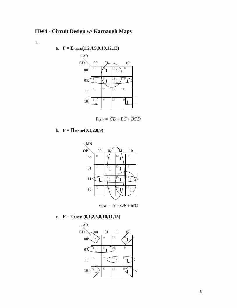

10
FSOP = ACD ACD BD+ +
d F = WXYZ (3671214)
FSOP = WY WZ X Z+ +
2
a F = XrsquoYrsquo + XrsquoZrsquo + WrsquoX + XYZ
FPOS = (Wrsquo + Xrsquo + Y)(X + Yrsquo + Zrsquo)(Wrsquo + Xrsquo + Z)
b The 4-bit prime numbers are 2 3 5 7 11 13
FPOS = (C+D)(Brsquo+D)(Arsquo+D)(Arsquo+B+C)
1
1
1
1
1 0
1 1
1 1 1 1
3
12 8
9 13 5 1
00 01 11 10
00
01
2 6
7 15
14 10
11
4
11
10
WX
YZ
0
1
1
1
1
0
0
1
1 0
1 0 1
1 0 1 1
3
12 8
9 13 5 1
00 01 11 10
00
01
2 6
7 15
14 10
11
4
11
10
WX
YZ
1
1
1
0
0
1
0
0 0
0 0 0
0 1 1 0
3
12 8
9 13 5 1
00 01 11 10
00
01
2 6
7 15
14 10
11
4
11
10
AB
CD
11
c The 4-bit numbers that are not perfect squares or cubes are 2 3 5 6 7
10 11 12 13 14 15
FPOS = (B + C)(A + C + D)
d The 4-bit numbers divisible by 3 or 5 are 0 3 5 6 9 10 12 15
FPOS = (A+B+C+Drsquo)(A+B+Crsquo+D)(A+Brsquo+C+D)(A+Brsquo+Crsquo+Drsquo)(Arsquo+B+C+D)bull
(Arsquo+B+Crsquo+Drsquo)(Arsquo+Brsquo+C+Drsquo)(Arsquo+Brsquo+Crsquo+D)
3 The K-Maps are below
FSOP = CD BC BCD+ +
1
1
1
1
1
1
1
1
0 0
0 1 0
0 1 1 0
3
12 8
9 13 5 1
00 01 11 10
00
01
2 6
7 15
14 10
11
4
11
10
AB
CD
1
0
0
1
1
0
0
1
1 0
0 1 0
1 0 1 0
3
12 8
9 13 5 1
00 01 11 10
00
01
2 6
7 15
14 10
11
4
11
10
AB
CD
1
1
0
1 1
1 1 1 1
3
12 8
9 13 5 1
00 01 11 10
00
01
2 6
7 15
14 10
11
4
11
10
AB
CD
12
FPOS = ( )( )( )C D B C B C D+ + + +
a AND ndash OR Implementation
B
Crsquo
D
CDrsquo
Brsquo
b OR - AND Implementation
Drsquo
Crsquo
Brsquo
CD
B
0
0
0
0
0
0
0 0
0
3
12 8
9 13 5 1
00 01 11 10
00
01
2 6
7 15
14 10
11
4
11
10
AB
CD
13
c NAND - NAND Implementation
B
Crsquo
D
CDrsquo
Brsquo
d NOR - NOR Implementation
Drsquo
Crsquo
Brsquo
CD
B
14
4
a The values with an odd number of 1s are 1 2 4 7 8 11 13 14 The
Donrsquot Care numbers are 0 4 5 8 10 12 and 15
SOP = ArsquoCrsquo + BD + AC + BrsquoDrsquo
b F = BrsquoCrsquoDrsquo + BCDrsquo + ABCrsquoD d = ArsquoBCrsquoD + ArsquoBrsquoCDrsquo
F = (A+Arsquo)BrsquoCrsquoDrsquo + (A+Arsquo)BCDrsquo + ABCrsquoD
= ABrsquoCrsquoDrsquo + ArsquoBrsquoCrsquoDrsquo + ABCDrsquo + ArsquoBCDrsquo + ABCrsquoD
d = ArsquoBCrsquoD + ArsquoBrsquoCDrsquo
FSOP = BrsquoCrsquoDrsquo + BCrsquoD + BCDrsquo
1
1
d
1
1
d
d 0
1 d 1
1 d 1
3
12 8
9 13 5 1
00 01 11 10
00
01
2 6
7 15
14 10
11
4
11
10
AB
CD
d
1
1
1 0
1
1 d
3
12 8
9 13 5 1
00 01 11 10
00
01
2 6
7 15
14 10
11
4
11
10
AB
CD
15
5
a F = ArsquoC + ACE + CABrsquo + BrsquoArsquoDE + Arsquo Drsquo Ersquo
FSOP = ArsquoC + ArsquoDrsquoErsquo + ArsquoBrsquoDE + BrsquoC + CE
b F = (AB + ArsquoBrsquo) (CrsquoDrsquo + CD)
= ABCrsquoDrsquo + ArsquoBrsquoCrsquoDrsquo + ABCD + ArsquoBrsquoCD
bull K-Map
FSOP = ABCrsquoDrsquo + ArsquoBrsquoCrsquoDrsquo + ABCD + ArsquoBrsquoCD
1
1
1 0
1
3
12 8
9 13 5 1
00 01 11 10
00
01
2 6
7 15
14 10
11
4
11
10
AB
CD
1
0
1
1
1
1
0
0
1 0
1 1 1
0 1 1
3
12 8
9 13 5 1
00 01 11 10
00
01
2 6
7 15
14 10
11
4
11
10
BC
DE
0
0
1
1
1
0
0
0
0 0
1 0 0
0 1 1 0
3
12 8
9 13 5 1
00 01 11 10
00
01
2 6
7 15
14 10
11
4
11
10
BC
DE
A=0 A=1
16
bull NAND ndash NAND Implementation
B
Crsquo
Drsquo
D
C
A
Arsquo
Brsquo
c F = ArsquoBrsquoCrsquoDrsquo + ArsquoBrsquoCDrsquo + ArsquoBCrsquoDrsquo + ArsquoBCrsquoD + ABrsquoCDrsquo
bull K-Map
FSOP = ArsquoCrsquoDrsquo + ArsquoBCrsquo + BrsquoCDrsquo
bull NAND ndash NAND Implementation
ArsquoCrsquo
Drsquo
B
Brsquo
C
1
1
1 0
1
1
3
12 8
9 13 5 1
00 01 11 10
00
01
2 6
7 15
14 10
11
4
11
10
AB
CD
F
F
17
d The numbers are 2 3 4 5 10 12 13 14 15
bull K-Map
SOP = AB + BCrsquo + ArsquoBrsquoC + ACDrsquo
bull NAND ndash NAND Implementation
A
B
Crsquo
ArsquoBrsquoC
Drsquo
1
1
1
1
1
0
1 1
1 1
3
12 8
9 13 5 1
00 01 11 10
00
01
2 6
7 15
14 10
11
4
11
10
AB
CD
18
6
a F = ArsquoC + ACE + CABrsquo + BrsquoArsquoDE + Arsquo Drsquo Ersquo
bull K-Map
FPOS = (Arsquo + Crsquo)(Arsquo + Brsquo + E)(Brsquo+C+Ersquo)(C + D + Ersquo)(C + Drsquo + E)
b F = (AB + ArsquoBrsquo) (CrsquoDrsquo + CD)
bull K-Map
FPOS = (A + Brsquo)(Arsquo + B)(C + Drsquo)(Crsquo + D)
0
0
0
0
0
0
0
0 0
0 0 0 0
3
12 8
9 13 5 1
00 01 11 10
00
01
2 6
7 15
14 10
11
4
11
10
AB
CD
1
0
1
1
1
1
0
0
1 0
1 1 1
0 1 1 0
3
12 8
9 13 5 1
00 01 11 10
00
01
2 6
7 15
14 10
11
4
11
10
BC
DE
0
0
1
1
1
0
0
0
0 0
1 0 0
0 1 1 0
3
12 8
9 13 5 1
00 01 11 10
00
01
2 6
7 15
14 10
11
4
11
10
BC
DE
A=0 A=1
19
NOR ndash NOR Implementation
A
Brsquo
Arsquo
B
CDrsquo
Crsquo
D
c F = ArsquoBrsquoCrsquoDrsquo + ArsquoBrsquoCDrsquo + ArsquoBCrsquoDrsquo + ArsquoBCrsquoD + ABrsquoCDrsquo
bull K-Map
FPOS = (B + Drsquo)(Brsquo + Crsquo)(Arsquo + C)
bull NOR ndash NOR Implementation
B
Drsquo
BrsquoCrsquo
ArsquoC
0
0
0
0
0
0
0
0 0
0 0 0
3
12 8
9 13 5 1
00 01 11 10
00
01
2 6
7 15
14 10
11
4
11
10
AB
CD
F
F
20
d The numbers are 2 3 4 5 10 12 13 14 15
bull K-Map
POS = (B + C)(A + Brsquo + Crsquo)(Arsquo + B + Drsquo)
bull NOR ndash NOR Implementation
BC
ABrsquoCrsquo
Arsquo
Drsquo
7 A and B are both 2-bit signed numbers They range from -2 to +1 Thus F = A + B
is ranging from -4 to +2 We need 3 bits to represent the signed number F
a The block diagram is below
A1
A0
B1
B0
F2
F1
F0
0
0
0
0 0
0
0 0
3
12 8
9 13 5 1
00 01 11 10
00
01
2 6
7 15
14 10
11
4
11
10
AB
CD
F
21
b The truth table is below
A1 A0 B1 B0 F2 F1 F0
0 0 0 0 0 0 0
0 0 0 1 0 0 1
0 0 1 0 1 1 0
0 0 1 1 1 1 1
0 1 0 0 0 0 1
0 1 0 1 0 1 0
0 1 1 0 1 1 1
0 1 1 1 0 0 0
1 0 0 0 1 1 0
1 0 0 1 1 1 1
1 0 1 0 1 0 0
1 0 1 1 1 0 1
1 1 0 0 1 1 1
1 1 0 1 0 0 0
1 1 1 0 1 0 1
1 1 1 1 1 1 0
c
K-Map of output ldquoF2rdquo K-Map of output ldquoF1rdquo
F2SOP = A1A0rsquo + B1B0rsquo + A1B1 + A1B0rsquo + A0rsquoB1
F1SOP = A1B1rsquoB0rsquo + A1A0rsquoB1rsquo + A1rsquoA0rsquoB1 + A1rsquoB1B0rsquo + A1rsquoA0B1rsquoB0 + A1A0B1B0
1
1
1
1
1
1
1
0
1 1
1
3
12 8
9 13 5 1
00 01 11 10
00
01
2 6
7 15
14 10
11
4
11
10
A1A0
B1B0
1
1
1
1
0
1 1
1 1
3
12 8
9 13 5 1
00 01 11 10
00
01
2 6
7 15
14 10
11
4
11
10
A1A0
B1B0
22
K-Map of output ldquoF0rdquo
F0SOP = A0B0rsquo + A0rsquoB0
d AND-OR implementation
Implementation of F2
A1A0
B1
B0
Implementation of F1
The implementation consists of four 3-input AND gates two 4-input AND gates and one
6-input OR gate
Implementation of F0
A0B0
A0
B0
1
1
1
1
0
1 1
1 1
3
12 8
9 13 5 1
00 01 11 10
00
01
2 6
7 15
14 10
11
4
11
10
A1A0
B1B0
23
NAND ndash NAND Implementation
(1) Implementation of F2
A1A0
B1
B0
(2) Implementation of F1
The implementation consists of four 3-input NAND gates two 4-input NAND gates and
one 6-input NAND gate
(3) Implementation of F0
A0B0
A0
B0
24
8 X is a 3-bit unsigned number It ranges from 0 to 7 Thus Y = 3X + 1 is ranging
from 1 to 22 We need 5 bits to represent the unsigned number Y
a The block diagram is below
X2
X1
X0
Y4
Y3Y2
Y1
Y0
b The truth table is below
X X2 X1 X0 Y4 Y3 Y2 Y1 Y0 Y
0 0 0 0 0 0 0 0 1 1
1 0 0 1 0 0 1 0 0 4
2 0 1 0 0 0 1 1 1 7
3 0 1 1 0 1 0 1 0 10
4 1 0 0 0 1 1 0 1 13
5 1 0 1 1 0 0 0 0 16
6 1 1 0 1 0 0 1 1 19
7 1 1 1 1 0 1 1 0 22
c
K-Map of output ldquoY4rdquo K-Map of output ldquoY3rdquo
Y4POS = X2(X1 + X0) Y3POS = (X2 + X1)(X1rsquo + X0)(X2rsquo + X0rsquo)
K-Map of output ldquoY2rdquo
Y2POS = (X2 + X1 + X0)( X2 + X1rsquo + X0rsquo)( X2rsquo + X1rsquo + X0)( X2rsquo + X1 + X0rsquo)
0 0
0 0
0 0
6 4
5 7 3 1
00 01 11 10
0
1
2
X2X1
X0
0 0
0 0
0 0 0
6 4
5 7 3 1
00 01 11 10
0
1
2
X2X1
X0
0 0
0
0 0
6 4
5 7 3 1
00 01 11 10
0
1
2
X2X1
X0
25
K-Map of output ldquoY1rdquo K-Map of output ldquoY0rdquo
Y1POS = X1 Y0POS = X0rsquo
d
bull OR ndash AND Implementation
Implementation of Y4
X1
X0
X2
Implementation of Y3
X2
X1
X1
X0
X2
X0
0 0
0
0 0
6 4
5 7 3 1
00 01 11 10
0
1
2
X2X1
X0
0
0 0 0 0
6 4
5 7 3 1
00 01 11 10
0
1
2
X2X1
X0
26
Implementation of Y2
X2X1X0
X1
X0
X2
Implementation of Y1 (straight wire connection)
Y1X1
Implementation of Y0 (straight wire connection)
Y0X0
bull NOR ndash NOR Implementation
Convert all gates in the above implementations to NOR gates For Y1 and Y0 just use
wires
27
e This will not be covered at this point of the class since we have not yet discussed
adders Ignore this question
9 X is a 3-bit signed number It ranges from -4 to +3
Thus Z = X2 + 2X + 1 = (X + 1)2 is ranging from 0 to +16 We need 6 bits to
represent signed number Z
a The block diagram is below
Z5
Z4
Z3
Z2Z1
Z0
X0
X1
X2
b The truth table is below
X X2 X1 X0 Z5 Z4 Z3 Z2 Z1 Z0 Z
+0 0 0 0 0 0 0 0 0 1 +1
+1 0 0 1 0 0 0 1 0 0 +4
+2 0 1 0 0 0 1 0 0 1 +9
+3 0 1 1 0 1 0 0 0 0 +16
-1 1 1 1 0 0 0 0 0 0 +0
-2 1 1 0 0 0 0 0 0 0 +1
-3 1 0 1 0 0 0 0 0 0 +4
-4 1 0 0 0 0 1 0 0 1 +9
c
No K-Map needed for Z5 ldquoZ5rdquo = 0
K-Map of output ldquoZ4rdquo K-Map of output ldquoZ3rdquo
Z4SOP = X2rsquoX1X0 Z3SOP = X2rsquoX1X0rsquo + X2X1rsquoX0rsquo
0
1
6 4
5 7 3 1
00 01 11 10
0
1
2
X2X1
X0
0
1 1
6 4
5 7 3 1
00 01 11 10
0
1
2
X2X1
X0
28
K-Map of output ldquoZ2rdquo K-Map of output ldquoZ0rdquo
Z2SOP = X2rsquoX1rsquoX0 Z0SOP = X2rsquoX0rsquo + X1rsquoX0rsquo
Note Z1 = 0 (constant)
0
1
6 4
5 7 3 1
00 01 11 10
0
1
2
X2X1
X0
1 0
1 1
6 4
5 7 3 1
00 01 11 10
0
1
2
X2X1
X0
29
10 Design a 1-bit comparator that takes in a bit X and a bit Y and outputs XltY
XgtY X=Y Use a single 2-to-4 decoder and 1 single OR gate
Consider the truth table of each of these simple functions We can implement
each as a sum of minterms And since a decoder implements the minterms of
the input variables we can arrive at the circuit above
X Y XltY XgtY X==Y
0 0 0 0 1
0 1 1 0 0
1 0 0 1 0
1 1 0 0 1
Y0
Y1
Y2
Y3
A0
A1
2-t
o-4
Decoder
X
Y XltY
XgtY
X=Y
30
HW5 - Signed Representations and Arithmetic
1
a
11 1
10100 = 20
+ 11101 = 29
Carry=1 110001 = 49
b
11100
- 10100
01000
28
- 20
8
1 1 1 1 _
11100
2rsquos comp 01011
+ 1
01000
2
b
1 1 1 1 _
101011
+ 011010
1000101
3 For unsigned subtraction we still use take the 2s complement of the bottom
number (but the check for overflow differs for unsigned vs 2s complement)
a 01101102 ndash 01001002 cannot be performed as is because we cannot
subtract a larger number from a smaller number in unsigned
representation
0110110
- 0100100
+54
-60
-6
1 1 1 1 1 1 _
0110110
2rsquos comp 1011011
+ 1
0010010
4
a Unsigned binary 28 lt 28310 lt 29 Therefore 9 bits 28310 = 1000110112
b 2rsquos complement with n-bits we can make ndash(2n-1) to +(2n-1-1) With n = 9
the range is -256 to +256 With n = 10 the range is -512 to +511 Thus
10 bits 28310 = 1000110112
5 Consider the following decimal numbers +21 +55 +121 -32 -99 -128
a What are the corresponding 8-bit signed-magnitude representation
31
a What are the corresponding 8-bit 2s complement representation
b Which of the above numbers can be represented in 6-bit signed-
magnitude 6-bit 1s complement 6-bit 2s complement representations
explain
21 55 121 -32 -99 -128 A 16+4+1=21
00010101 00110111 01111001 10100000 11100011 NA
B 00010101 00110111 01111001 1110000 10011101 10000000 C YYY
010101 in all cases
NNN NNN NNY 100000 in 2rsquos comp
NNN NNN
6 What are the corresponding decimal representations for the following binary
numbers 01011011 11010010 if
a The binary numbers are in 8-bit signed-magnitude format
b The binary numbers are in 8-bit 2s complement format
01011011 11010010 a) 64+16+8+2+1=91 -(64+16+2)=-82 b) 64+16+8+2+1=91 -128+64+16+2=-46
7 Perform the following addition problems for the following 2rsquos complement
numbers State whether overflow does or does not occur for each problem
Justify your answer for why overflow does or does not occur Check your
work by converting each number to decimal
a 1010 0111 b 1001 0110 c 0101 1100 d 0101 1101
+1110 0100 +1011 0011 +1011 0101 +0110 1001
11000 1011 10100 1001 10001 0001 1100 0110
n+n=n
cin=cout=1
No Overflow
n+n=p
cin=0cout=1
Overflow
p+n=p
cin=cout=1
NoOverflow
p+p=n
cin=1cout=0
Overflow
8 This is an exercise to help you remember what gates are used to create a full
adder Using a full adder as shown below and no other gates can you
produce the function Z = AbullB (Hint Write out the logical equations for S
and Cout and see if you can hook up the inputs to produce Z)
ANSWER
Cin X Y S Cout
0 0 0 0 0
32
0 0 1 1 0
0 1 0 1 0
0 1 1 0 1
1 0 0 1 0
1 0 1 0 1
1 1 0 0 1
1 1 1 1 1
S X Y Cin
Cout XY XCin YCin
=
= + +
We want Z=XY and if we set Cin=0 then the formulas of S and Cout
becomes as follows
S X Y
Cout XY
=
=
Thus Cout = Z = XY
X Y
S
CinFull Adder
Cout
A B
0Z
33
9 Using 1 half-adder and a minimal number of 4-bit binary adders design a
circuit to calculate Y = 25X where X is a 4-bit inputs
ANSWER
If a number is multiplied by a number that is a power of 2 then the number rewritten
using the above formula
2 00
n
n X X=
Y = 25X = 16X + 8X + X = X0000+X000+X
Also adding the information that X is a 4-bit number above formula can be re-written
X = X3X2X1X0
Y = X3X2X1X00000 + X3X2X1X0000 + X3X2X1X0
This can be written as addition by 4 bit adders
X3 X2 X1 X0
X3 X2 X1 X0 0 0 0
+ X3 X2 X1 X0 0 0 0 0
Since one row in each addition is all zeros they can be eliminated and the other two
numbers can be added using a 4-bit adder However the lower bits require only a single
bit adder The carry from the first addition is transferred to the next one
B3 B2 B1 B0 A3 A2 A1 A0
S0S1S2S3
C0C4 4-bit Binary Adder
X Y
S
Half AdderCout
X3 X0X0X1X2X3 X1X2X30 X0X1X2
Y8 Y7 Y6 Y5 Y4 Y3 Y0Y1Y2
34
10 Using a minimal number of 4-bit adders design a circuit that implements
Y=20X+107 where X is a 3-bit unsigned number
ANSWER
X = X2X1X0 and thus 20X= 16X+4X These numbers are achieved by inserting zeros
at the end Once we add these there numbers we see that not all bits require addition We
actually need only a single 4-bit adder and nothing more
1 1 0 1 0 1 1
X2 X1 X0 0 0
+ X2 X1 X0 0 0 0 0
Which can be collapsed to the following addition
1 1 X2 X1 X0 0 0
+ X2 X1 X0 1 0 1 1
B3 B2 B1 B0 A3 A2 A1 A0
S0S1S2S3
C0C4 4-bit Binary Adder
X0X1X2 X1X211
11
X0
Y7 Y6 Y5 Y4 Y3 Y0Y1Y2
0
1
35
11 Design a minimal circuit using ANDORNOT gates to implement the
comparison A gt 10 where A is a 4-bit number
a Start by writing out the logical algorithm for when A gt 10 then implement it
using gates
b Check that your work is minimal by using a K-Map
ANSWER
Letrsquos assume that the number A = A3A2A1A0
Logical Algorithm For any number A to be greater than a number B (in this case 1010 =
10102) a more significant bit of A must be greater than B However in the case of A
compared with 1010 we realize A3 and A1 can never be greater than the 1rsquos in those
places for 10 Similarly A2 and A0 can never be less than the 0rsquos in those places Thus
for A gt 10 there are only 2 cases that need to be checked
A3 = 1 and A2 gt 0 (ie A2 = 1)
OR
A3=1 and A1 = 1 and A0 gt 0 (ie A0 = 1)
Thus Agt10 = A3A2 + A3A2A0
Note that we donrsquot have to check A2 in the second case because it is DEFINITELY
greater than or equal to the 0 in that place of 10102
A K-Map will also show the same equation
SUM(1112131415)
Agt10=A3A2+ A3A1A0
A3
A2
A3
A0A1
Agt10
1
1
1
0
1
1
3
12 8
9 13 5 1
00 01 11 10
00
01
2 6
7 15
14 10
11
4
11
10
A3A2
A1A0
36
HW 6 ndash Latches and Flip-Flops
1 Complete the following waveforms for negative edge-triggered D Flip-Flops
D Q
QCK
D Q
QCK
CLK
D1
D2D1
D2
Z
X
CLK
X
D1
D2
Z
2 We should find the state diagram following the steps in the class notes
a Convert the diagram to a table
Current
State
Next State Output
XY= 00 XY= 01 XY= 10 XY= 11
Q1 Q0 Q1 Q0
Q1
Q0 Q1
Q0 Q1
Q0 Z
0 0 0 0 0 0 1 0 1 0 0
0 1 0 0 0 0 0 1 0 1 1
1 0 0 0 0 1 0 0 0 1 0
1 1 0 0 0 1 0 1 0 1 0
37
Convert Q to D
Current
State
Next State Output
XY= 00 XY= 01 XY= 10 XY= 11
Q1 Q0 D1 D0 D1 D0 D1 D0 D1 D0 Z
0 0 0 0 0 0 1 0 1 0 0
0 1 0 0 0 0 0 1 0 1 1
1 0 0 0 0 1 0 0 0 1 0
1 1 0 0 0 1 0 1 0 1 0
b Perform K-maps to find equations for D1 and D0
D0 = Q1Y + Q0X
D1 = Q1rsquoQ0rsquoX
c Draw the circuit and implement the initial state (reset) condition
D Q
QCK
D Q
QCK
ZX
Clock
Q0
Q1Y
PRE PRE
CLR CLR
Reset Reset
GND GND
38
3 Because we have 2 states in the state diagram we use one D flip-flop to
implement state memory We design the combinational logic for the next-state
logic and the output function logic by building up the statetransition table
Current State Next State Output
XY = 00 XY = 01 XY = 10 XY = 11
SymbolCode SymbolCode SymbolCode SymbolCode SymbolCode H
F 0 F 0 G 1 G 1 G 1 0
G 1 F 0 F 0 F 0 G 1 1 Q0(t) Q0
D0 Q0
D0 Q0
D0 Q0
D0
After we get the statetransition table we build the K-Maps to simplify expressions for
D0 and H
bull D0 K-Map
D0 = YQ0rsquo + XQ0rsquo + XY H = Q0
0
1 1 1
1
6 4
5 7 3 1
00 01 11 10
0
1
2
XY
Q0
39
4
Current State Next State amp Flop-Flop Inputs Outputs
Next State Next State
X = 0 X = 1
SymbolCode SymbolCode SymbolCode Z
A00 B01 D11 0
B01 C10 B01 0
C10 B01 A00 1
D11 B01 C10 0 Q1(t)Q0(t) Q1(t+1)Q0(t+1) Q1(t+1)Q0(t+1)
After we get the statetransition table we build the K-Maps to simplify expressions for
D1 D0 and Z
bull D1 K-Map D0 K-Map
D1 = XrsquoQ1Q0 + XQ0rsquo D0 = XrsquoQ1+XQ0 + XQ1rsquo
Z K-Map
Z = Q1Q0rsquo
1
1 0
0 1
1 0
1 00
01
11
10
0 Q1Q0
X
1
1
0 0
1 0
0 1
0 00
01
11
10
0 Q1Q0
X
1
1
0 0
0 0
1
0 Q0
Q1
1
40
a The waveform is below
CLK
X
Q1
Q0
State
Z
A D B C A B
41
5
a We need 4 states and each of them stores one 2-bit binary number ranging
from 00 to 11
State S0 S1 S2 S3
Assignment
(Q1 Q0)
00 01 10 11
The state diagram is below
b Because we have 4 states in the state diagram we use two D flip-flops to
implement state memory We design the combinational logic for the next-
state logic and the output function logic by building up the statetransition
table
U ndash UP D ndash DOWN
Current State Next State
UD = 00 UD = 01 UD = 10 UD = 11
SymbolCode SymbolCode SymbolCode SymbolCode SymbolCode
S000 S000 S311 S101 S000
S101 S101 S000 S210 S101
S210 S210 S101 S311 S210
S311 S311 S210 S000 S311 Q1(t)Q0(t) Q1(t+1)Q0(t+1)
D1D0 Q1(t+1)Q0(t+1)
D1D0 Q1(t+1)Q0(t+1)
D1D0 Q1(t+1)Q0(t+1)
D1D0
After we get the statetransition table we build the K-Maps to simplify expressions for
D1 and D0
S0 S1 S2 S3
UP=DOWN=1 or
UP=DOWN=0
UP=DOWN=1 or
UP=DOWN=0
UP=DOWN=1 or
UP=DOWN=0UP=DOWN=1 or
UP=DOWN=0
UP=1 and
DOWN=0
UP=1 and
DOWN=0UP=1 and
DOWN=0
UP=1 and DOWN=0
UP=0 and
DOWN=1UP=0 and
DOWN=1
UP=0 and
DOWN=1
UP=0 and DOWN=1
~R
ese
t
42
bull D1 K-Map
D1 = UrsquoDrsquoQ1 + DQ1Q0 + UQ1Q0rsquo + UrsquoDQ1rsquoQ0rsquo + UDrsquoQ1rsquoQ0
bull D0 K-Map
D0 = UrsquoDrsquoQ0 + UDQ0 + UrsquoDQ0rsquo + UDrsquoQ0rsquo
c The waveform is below
CLK
UP
DOWN
Q1
Q0
1
1
1
1
1
1
0
1
1
3
12 8
9 13 5 1
00 01 11 10
00
01
2 6
7 15
14 10
11
4
11
10
UD
Q1Q0
1
1
1
1
0
1 1
1 1
3
12 8
9 13 5 1
00 01 11 10
00
01
2 6
7 15
14 10
11
4
11
10
UD
Q1Q0
43
6 Complete the waveform for the 4-bit counter presented in class
1111
Clock
SR
CEP
CET
PE
P3-P0
Q3-Q0 1101
1101
1110 0000 0001 0000 1110 1111
7 Complete the waveform for a 4-bit D-Register with Data (Load) Enable and
asynchronous reset
CLK
AR
EN
0110D[30] 0001 10111010 11011001 10001111 0111
Q[30] 1010 11111101 10000000 1011
44
81 Unit 7 ndash Datapath Design 1 Implement a circuit that takes in a 4-bit number X[30] and produces a 4-bit value
Z[30] according to the following function
if X lt 8 then
Z = X + 5
else
Z = X ndash 2
Using the building blocks below and at most 1 inverter (no other gates)
implement this function
Note To check Xlt8 subtract X-8 by taking the 2rsquos complement of 8 The 2rsquos comp of
8 is 0111+1 Recall a carry of 0 when subtracting unsigned numbers (A-B) indicates
overflow which can only occur in unsigned subtraction if the result needed to be negative
(ie A lt B) So C4 will only be 1 if X is not less-than 8 We can invert it to get a signal
that is true when X lt 8 Use those signals to either add 5 (0101) or subtract 2 (add 1110)
B3 B2 B1 B0 A3 A2 A1 A0
S0S1S2S3
C0C4 4-bit Binary Adder
X lt 8
Xlt8
X0X1X2X3
Z0Z1Z2Z3
B3
B2
B1
B0
A3
A2
A1
A0
S0
S1
S2
S3
C0
C4
4-b
it B
inary
Add
er
X3
X2
X1
X0
1
1
1
0
1
0
1
45
2 Design a circuit that takes in an 4-bit number X[30] and outputs a number Y and
performs the operation below Assume these numbers are unsigned Use a 4-bit
adder and 2-to-1 muxes Hint Multiplying by 4 (ie 22) in binary can be done with
no gates just as multiplying by 100 (ie 102) in decimal can be done simply and
easily
if(X lt 00112)
Y = 4X
else
Y = X
4X would require 6 outputs and be X3 X2 X1 X0 0 0 thus even if we pass X we need to
produce 6 outputs Recall subtracting 3=0011 bin is the same as adding the 2s
complement Next a carry of 0 when subtracting unsigned numbers (A-B) indicates
overflow which can only occur in unsigned subtraction if the result needed to be negative
(ie A lt B)
I1
Y
S
I0
I1
Y
S
I0
I1
Y
S
I0
I1
Y
S
I0
I1
Y
S
I0
I1
Y
S
I0
X0
X1
X2
X3
0
0
0
0
X0
X1
X2
X3
Y5
Y4
Y3
Y2
Y0
Y1
X lt 3
B3
B2
B1
B0
A3
A2
A1
A0
S0
S1
S2
S3
C0
C4
4-b
it B
inary
Add
er
X3
X2
X1
X0
0
0
1
1
1
46
3 Design a circuit that takes in two 4-bit numbers X[30] and Y[30] along with two
function select bits FS1 and FS0 and produces an output Z[30] according to the
following table
FS1FS0 Z
00 X+Y
01 X-Y
10 Y-X
11 donrsquot care
Use (1) 4-bit adder 4-bit wide 2-to-1 muxes and any basic gates you desire
Approach Take a 4-bit adder and for each operation listed in the table above
identify what should be passed to the A and B inputs of the adder Then use
muxes to perform that function Design logic for the select bits of the muxes and
the carry-in of the adder that use FS1 and FS0 as input
Note In the solution below the A and B inputs of the muxes are like the 0th and
1st inputs of 4 2-to-1 muxes respectively Ignore the G input
B3
B2
B1
B0
A3
A2
A1
A0
S3
S2
S1
S0
C0
C4
S
G
1A
1Y
2Y
2-to-1
4-bit
wide
mux
2A
3A
4A3Y
4Y1B
2B
3B
4B
0
S
G
1A
1Y
2Y
2-to-1
4-bit
wide
mux
2A
3A
4A3Y
4Y1B
2B
3B
4B
0
X3
X2
X1
X0
X3
X2
X1
X0
Y3
Y2
Y1
Y0
Y3
Y2
Y1
Y0
Z3
Z2
Z1
Z0
FS1
FS0
FS1FS0
74LS
283
47
4 Design a circuit that takes in two 4-bit signed magnitude numbers X[30] and
Y[30] and produces two 4-bit outputs A[30] and B[30] according to the following
algorithm
if X gt= Y then
A = X and B = Y
else
A = Y and B = X
Use a 4-bit adder to subtract and perform the comparison 4-bit wide 2-to-1
muxes and basic logic gates Assume the input 1000 = -0 will never occur on X
or Y
Approach First think about how to compare signed magnitude numbers by using
unsigned comparison techniques and how to precondition the inputs to allow the
use of unsigned comparison For example 1001 = -1 in signed magnitude and
0100 = +4 in signed magnitude So 1001 is really less than 0100 Use the
comparison result to control the selects of the muxes
Y0
Y1
Y2
Y3
X0
X1
X2
X3
XgtY
S
G
1A
1Y
2Y
2-to-1
4-bit
wide
mux
2A
3A
4A3Y
4Y1B
2B
3B
4B
0
S
G
1A
1Y
2Y
2-to-1
4-bit
wide
mux
2A
3A
4A3Y
4Y1B
2B
3B
4B
0
X3
X2
X1
X0
Y3
Y2
Y1
Y0
X3
X2
X1
X0
Y3
Y2
Y1
Y0
A3
A2
A1
A0
B3
B2
B1
B0
B3
B2
B1
B0
A3
A2
A1
A0
S0
S1
S2
S3
C0
C4
4-b
it B
inary
Add
er
1
48
5 Design a circuit that adds two 4-bit unsigned numbers X[30] and Y[30] and
outputs either the sum if there is no overflow or 1111 (=1510 the maximum unsigned
4-bit number) if there is overflow
Unsigned overflow is found by looking at Cout You could use a mux to select the sum
or 1111 but realize you can just use OR gates for this function
B3
B2
B1
B0
A3
A2
A1
A0
S3
S2
S1
S0
C0
C4
74LS
283
X3
X2
X1
X0
UNS_OV
0
Y3
Y2
Y1
Y0
G0
G1
G2
G3
49
1 We would like to build an adder whose inputs are in units of pennies and produces
sum in nickels and pennies Essentially this is a base-5 adder The 2 inputs of this
adder are A=A2A1A0 and B=B2B1B0 Assume that the maximum input number
that A and B can be is 4 pennies Design an adder to produce the correct
nickelspennies sum C= [CN] [CP2CP1CP0] To implement this design you may
assume you can use as many 4-bit adders as you like
if X+Y gt 4 dec then
CN = 1 CP[20] = X+Y-5
else
CN = 0 CP[20] = X+Y
A2 A1 A0 B2 B1 B0
CP2 CP1 CP0
To be designed by you
CN
Block diagram for the
nickelpenny adder you
are going to design
50
B3 B2 B1 B0 A3 A2 A1 A0
S0S1S2S3
C0C4 4-bit Binary Adder
Z4 Z2 Z1
CP2
0
0
B3 B2 B1 B0 A3 A2 A1 A0
S0S1S2S3
C0C4 4-bit Binary Adder
0 X4 X2 X1 0 Y4 Y2 Y1
Z8 Z4 Z2 Z1
0
B3 B2 B1 B0 A3 A2 A1 A0
S0S1S2S3
C0C4 4-bit Binary Adder
0 1 0 0 Z8 Z4 Z2 Z1
1
Need actual
inverters here
just didn t
draw them
CN
(4 lt X+Y)
CP1 CP0

11
c The 4-bit numbers that are not perfect squares or cubes are 2 3 5 6 7
10 11 12 13 14 15
FPOS = (B + C)(A + C + D)
d The 4-bit numbers divisible by 3 or 5 are 0 3 5 6 9 10 12 15
FPOS = (A+B+C+Drsquo)(A+B+Crsquo+D)(A+Brsquo+C+D)(A+Brsquo+Crsquo+Drsquo)(Arsquo+B+C+D)bull
(Arsquo+B+Crsquo+Drsquo)(Arsquo+Brsquo+C+Drsquo)(Arsquo+Brsquo+Crsquo+D)
3 The K-Maps are below
FSOP = CD BC BCD+ +
1
1
1
1
1
1
1
1
0 0
0 1 0
0 1 1 0
3
12 8
9 13 5 1
00 01 11 10
00
01
2 6
7 15
14 10
11
4
11
10
AB
CD
1
0
0
1
1
0
0
1
1 0
0 1 0
1 0 1 0
3
12 8
9 13 5 1
00 01 11 10
00
01
2 6
7 15
14 10
11
4
11
10
AB
CD
1
1
0
1 1
1 1 1 1
3
12 8
9 13 5 1
00 01 11 10
00
01
2 6
7 15
14 10
11
4
11
10
AB
CD
12
FPOS = ( )( )( )C D B C B C D+ + + +
a AND ndash OR Implementation
B
Crsquo
D
CDrsquo
Brsquo
b OR - AND Implementation
Drsquo
Crsquo
Brsquo
CD
B
0
0
0
0
0
0
0 0
0
3
12 8
9 13 5 1
00 01 11 10
00
01
2 6
7 15
14 10
11
4
11
10
AB
CD
13
c NAND - NAND Implementation
B
Crsquo
D
CDrsquo
Brsquo
d NOR - NOR Implementation
Drsquo
Crsquo
Brsquo
CD
B
14
4
a The values with an odd number of 1s are 1 2 4 7 8 11 13 14 The
Donrsquot Care numbers are 0 4 5 8 10 12 and 15
SOP = ArsquoCrsquo + BD + AC + BrsquoDrsquo
b F = BrsquoCrsquoDrsquo + BCDrsquo + ABCrsquoD d = ArsquoBCrsquoD + ArsquoBrsquoCDrsquo
F = (A+Arsquo)BrsquoCrsquoDrsquo + (A+Arsquo)BCDrsquo + ABCrsquoD
= ABrsquoCrsquoDrsquo + ArsquoBrsquoCrsquoDrsquo + ABCDrsquo + ArsquoBCDrsquo + ABCrsquoD
d = ArsquoBCrsquoD + ArsquoBrsquoCDrsquo
FSOP = BrsquoCrsquoDrsquo + BCrsquoD + BCDrsquo
1
1
d
1
1
d
d 0
1 d 1
1 d 1
3
12 8
9 13 5 1
00 01 11 10
00
01
2 6
7 15
14 10
11
4
11
10
AB
CD
d
1
1
1 0
1
1 d
3
12 8
9 13 5 1
00 01 11 10
00
01
2 6
7 15
14 10
11
4
11
10
AB
CD
15
5
a F = ArsquoC + ACE + CABrsquo + BrsquoArsquoDE + Arsquo Drsquo Ersquo
FSOP = ArsquoC + ArsquoDrsquoErsquo + ArsquoBrsquoDE + BrsquoC + CE
b F = (AB + ArsquoBrsquo) (CrsquoDrsquo + CD)
= ABCrsquoDrsquo + ArsquoBrsquoCrsquoDrsquo + ABCD + ArsquoBrsquoCD
bull K-Map
FSOP = ABCrsquoDrsquo + ArsquoBrsquoCrsquoDrsquo + ABCD + ArsquoBrsquoCD
1
1
1 0
1
3
12 8
9 13 5 1
00 01 11 10
00
01
2 6
7 15
14 10
11
4
11
10
AB
CD
1
0
1
1
1
1
0
0
1 0
1 1 1
0 1 1
3
12 8
9 13 5 1
00 01 11 10
00
01
2 6
7 15
14 10
11
4
11
10
BC
DE
0
0
1
1
1
0
0
0
0 0
1 0 0
0 1 1 0
3
12 8
9 13 5 1
00 01 11 10
00
01
2 6
7 15
14 10
11
4
11
10
BC
DE
A=0 A=1
16
bull NAND ndash NAND Implementation
B
Crsquo
Drsquo
D
C
A
Arsquo
Brsquo
c F = ArsquoBrsquoCrsquoDrsquo + ArsquoBrsquoCDrsquo + ArsquoBCrsquoDrsquo + ArsquoBCrsquoD + ABrsquoCDrsquo
bull K-Map
FSOP = ArsquoCrsquoDrsquo + ArsquoBCrsquo + BrsquoCDrsquo
bull NAND ndash NAND Implementation
ArsquoCrsquo
Drsquo
B
Brsquo
C
1
1
1 0
1
1
3
12 8
9 13 5 1
00 01 11 10
00
01
2 6
7 15
14 10
11
4
11
10
AB
CD
F
F
17
d The numbers are 2 3 4 5 10 12 13 14 15
bull K-Map
SOP = AB + BCrsquo + ArsquoBrsquoC + ACDrsquo
bull NAND ndash NAND Implementation
A
B
Crsquo
ArsquoBrsquoC
Drsquo
1
1
1
1
1
0
1 1
1 1
3
12 8
9 13 5 1
00 01 11 10
00
01
2 6
7 15
14 10
11
4
11
10
AB
CD
18
6
a F = ArsquoC + ACE + CABrsquo + BrsquoArsquoDE + Arsquo Drsquo Ersquo
bull K-Map
FPOS = (Arsquo + Crsquo)(Arsquo + Brsquo + E)(Brsquo+C+Ersquo)(C + D + Ersquo)(C + Drsquo + E)
b F = (AB + ArsquoBrsquo) (CrsquoDrsquo + CD)
bull K-Map
FPOS = (A + Brsquo)(Arsquo + B)(C + Drsquo)(Crsquo + D)
0
0
0
0
0
0
0
0 0
0 0 0 0
3
12 8
9 13 5 1
00 01 11 10
00
01
2 6
7 15
14 10
11
4
11
10
AB
CD
1
0
1
1
1
1
0
0
1 0
1 1 1
0 1 1 0
3
12 8
9 13 5 1
00 01 11 10
00
01
2 6
7 15
14 10
11
4
11
10
BC
DE
0
0
1
1
1
0
0
0
0 0
1 0 0
0 1 1 0
3
12 8
9 13 5 1
00 01 11 10
00
01
2 6
7 15
14 10
11
4
11
10
BC
DE
A=0 A=1
19
NOR ndash NOR Implementation
A
Brsquo
Arsquo
B
CDrsquo
Crsquo
D
c F = ArsquoBrsquoCrsquoDrsquo + ArsquoBrsquoCDrsquo + ArsquoBCrsquoDrsquo + ArsquoBCrsquoD + ABrsquoCDrsquo
bull K-Map
FPOS = (B + Drsquo)(Brsquo + Crsquo)(Arsquo + C)
bull NOR ndash NOR Implementation
B
Drsquo
BrsquoCrsquo
ArsquoC
0
0
0
0
0
0
0
0 0
0 0 0
3
12 8
9 13 5 1
00 01 11 10
00
01
2 6
7 15
14 10
11
4
11
10
AB
CD
F
F
20
d The numbers are 2 3 4 5 10 12 13 14 15
bull K-Map
POS = (B + C)(A + Brsquo + Crsquo)(Arsquo + B + Drsquo)
bull NOR ndash NOR Implementation
BC
ABrsquoCrsquo
Arsquo
Drsquo
7 A and B are both 2-bit signed numbers They range from -2 to +1 Thus F = A + B
is ranging from -4 to +2 We need 3 bits to represent the signed number F
a The block diagram is below
A1
A0
B1
B0
F2
F1
F0
0
0
0
0 0
0
0 0
3
12 8
9 13 5 1
00 01 11 10
00
01
2 6
7 15
14 10
11
4
11
10
AB
CD
F
21
b The truth table is below
A1 A0 B1 B0 F2 F1 F0
0 0 0 0 0 0 0
0 0 0 1 0 0 1
0 0 1 0 1 1 0
0 0 1 1 1 1 1
0 1 0 0 0 0 1
0 1 0 1 0 1 0
0 1 1 0 1 1 1
0 1 1 1 0 0 0
1 0 0 0 1 1 0
1 0 0 1 1 1 1
1 0 1 0 1 0 0
1 0 1 1 1 0 1
1 1 0 0 1 1 1
1 1 0 1 0 0 0
1 1 1 0 1 0 1
1 1 1 1 1 1 0
c
K-Map of output ldquoF2rdquo K-Map of output ldquoF1rdquo
F2SOP = A1A0rsquo + B1B0rsquo + A1B1 + A1B0rsquo + A0rsquoB1
F1SOP = A1B1rsquoB0rsquo + A1A0rsquoB1rsquo + A1rsquoA0rsquoB1 + A1rsquoB1B0rsquo + A1rsquoA0B1rsquoB0 + A1A0B1B0
1
1
1
1
1
1
1
0
1 1
1
3
12 8
9 13 5 1
00 01 11 10
00
01
2 6
7 15
14 10
11
4
11
10
A1A0
B1B0
1
1
1
1
0
1 1
1 1
3
12 8
9 13 5 1
00 01 11 10
00
01
2 6
7 15
14 10
11
4
11
10
A1A0
B1B0
22
K-Map of output ldquoF0rdquo
F0SOP = A0B0rsquo + A0rsquoB0
d AND-OR implementation
Implementation of F2
A1A0
B1
B0
Implementation of F1
The implementation consists of four 3-input AND gates two 4-input AND gates and one
6-input OR gate
Implementation of F0
A0B0
A0
B0
1
1
1
1
0
1 1
1 1
3
12 8
9 13 5 1
00 01 11 10
00
01
2 6
7 15
14 10
11
4
11
10
A1A0
B1B0
23
NAND ndash NAND Implementation
(1) Implementation of F2
A1A0
B1
B0
(2) Implementation of F1
The implementation consists of four 3-input NAND gates two 4-input NAND gates and
one 6-input NAND gate
(3) Implementation of F0
A0B0
A0
B0
24
8 X is a 3-bit unsigned number It ranges from 0 to 7 Thus Y = 3X + 1 is ranging
from 1 to 22 We need 5 bits to represent the unsigned number Y
a The block diagram is below
X2
X1
X0
Y4
Y3Y2
Y1
Y0
b The truth table is below
X X2 X1 X0 Y4 Y3 Y2 Y1 Y0 Y
0 0 0 0 0 0 0 0 1 1
1 0 0 1 0 0 1 0 0 4
2 0 1 0 0 0 1 1 1 7
3 0 1 1 0 1 0 1 0 10
4 1 0 0 0 1 1 0 1 13
5 1 0 1 1 0 0 0 0 16
6 1 1 0 1 0 0 1 1 19
7 1 1 1 1 0 1 1 0 22
c
K-Map of output ldquoY4rdquo K-Map of output ldquoY3rdquo
Y4POS = X2(X1 + X0) Y3POS = (X2 + X1)(X1rsquo + X0)(X2rsquo + X0rsquo)
K-Map of output ldquoY2rdquo
Y2POS = (X2 + X1 + X0)( X2 + X1rsquo + X0rsquo)( X2rsquo + X1rsquo + X0)( X2rsquo + X1 + X0rsquo)
0 0
0 0
0 0
6 4
5 7 3 1
00 01 11 10
0
1
2
X2X1
X0
0 0
0 0
0 0 0
6 4
5 7 3 1
00 01 11 10
0
1
2
X2X1
X0
0 0
0
0 0
6 4
5 7 3 1
00 01 11 10
0
1
2
X2X1
X0
25
K-Map of output ldquoY1rdquo K-Map of output ldquoY0rdquo
Y1POS = X1 Y0POS = X0rsquo
d
bull OR ndash AND Implementation
Implementation of Y4
X1
X0
X2
Implementation of Y3
X2
X1
X1
X0
X2
X0
0 0
0
0 0
6 4
5 7 3 1
00 01 11 10
0
1
2
X2X1
X0
0
0 0 0 0
6 4
5 7 3 1
00 01 11 10
0
1
2
X2X1
X0
26
Implementation of Y2
X2X1X0
X1
X0
X2
Implementation of Y1 (straight wire connection)
Y1X1
Implementation of Y0 (straight wire connection)
Y0X0
bull NOR ndash NOR Implementation
Convert all gates in the above implementations to NOR gates For Y1 and Y0 just use
wires
27
e This will not be covered at this point of the class since we have not yet discussed
adders Ignore this question
9 X is a 3-bit signed number It ranges from -4 to +3
Thus Z = X2 + 2X + 1 = (X + 1)2 is ranging from 0 to +16 We need 6 bits to
represent signed number Z
a The block diagram is below
Z5
Z4
Z3
Z2Z1
Z0
X0
X1
X2
b The truth table is below
X X2 X1 X0 Z5 Z4 Z3 Z2 Z1 Z0 Z
+0 0 0 0 0 0 0 0 0 1 +1
+1 0 0 1 0 0 0 1 0 0 +4
+2 0 1 0 0 0 1 0 0 1 +9
+3 0 1 1 0 1 0 0 0 0 +16
-1 1 1 1 0 0 0 0 0 0 +0
-2 1 1 0 0 0 0 0 0 0 +1
-3 1 0 1 0 0 0 0 0 0 +4
-4 1 0 0 0 0 1 0 0 1 +9
c
No K-Map needed for Z5 ldquoZ5rdquo = 0
K-Map of output ldquoZ4rdquo K-Map of output ldquoZ3rdquo
Z4SOP = X2rsquoX1X0 Z3SOP = X2rsquoX1X0rsquo + X2X1rsquoX0rsquo
0
1
6 4
5 7 3 1
00 01 11 10
0
1
2
X2X1
X0
0
1 1
6 4
5 7 3 1
00 01 11 10
0
1
2
X2X1
X0
28
K-Map of output ldquoZ2rdquo K-Map of output ldquoZ0rdquo
Z2SOP = X2rsquoX1rsquoX0 Z0SOP = X2rsquoX0rsquo + X1rsquoX0rsquo
Note Z1 = 0 (constant)
0
1
6 4
5 7 3 1
00 01 11 10
0
1
2
X2X1
X0
1 0
1 1
6 4
5 7 3 1
00 01 11 10
0
1
2
X2X1
X0
29
10 Design a 1-bit comparator that takes in a bit X and a bit Y and outputs XltY
XgtY X=Y Use a single 2-to-4 decoder and 1 single OR gate
Consider the truth table of each of these simple functions We can implement
each as a sum of minterms And since a decoder implements the minterms of
the input variables we can arrive at the circuit above
X Y XltY XgtY X==Y
0 0 0 0 1
0 1 1 0 0
1 0 0 1 0
1 1 0 0 1
Y0
Y1
Y2
Y3
A0
A1
2-t
o-4
Decoder
X
Y XltY
XgtY
X=Y
30
HW5 - Signed Representations and Arithmetic
1
a
11 1
10100 = 20
+ 11101 = 29
Carry=1 110001 = 49
b
11100
- 10100
01000
28
- 20
8
1 1 1 1 _
11100
2rsquos comp 01011
+ 1
01000
2
b
1 1 1 1 _
101011
+ 011010
1000101
3 For unsigned subtraction we still use take the 2s complement of the bottom
number (but the check for overflow differs for unsigned vs 2s complement)
a 01101102 ndash 01001002 cannot be performed as is because we cannot
subtract a larger number from a smaller number in unsigned
representation
0110110
- 0100100
+54
-60
-6
1 1 1 1 1 1 _
0110110
2rsquos comp 1011011
+ 1
0010010
4
a Unsigned binary 28 lt 28310 lt 29 Therefore 9 bits 28310 = 1000110112
b 2rsquos complement with n-bits we can make ndash(2n-1) to +(2n-1-1) With n = 9
the range is -256 to +256 With n = 10 the range is -512 to +511 Thus
10 bits 28310 = 1000110112
5 Consider the following decimal numbers +21 +55 +121 -32 -99 -128
a What are the corresponding 8-bit signed-magnitude representation
31
a What are the corresponding 8-bit 2s complement representation
b Which of the above numbers can be represented in 6-bit signed-
magnitude 6-bit 1s complement 6-bit 2s complement representations
explain
21 55 121 -32 -99 -128 A 16+4+1=21
00010101 00110111 01111001 10100000 11100011 NA
B 00010101 00110111 01111001 1110000 10011101 10000000 C YYY
010101 in all cases
NNN NNN NNY 100000 in 2rsquos comp
NNN NNN
6 What are the corresponding decimal representations for the following binary
numbers 01011011 11010010 if
a The binary numbers are in 8-bit signed-magnitude format
b The binary numbers are in 8-bit 2s complement format
01011011 11010010 a) 64+16+8+2+1=91 -(64+16+2)=-82 b) 64+16+8+2+1=91 -128+64+16+2=-46
7 Perform the following addition problems for the following 2rsquos complement
numbers State whether overflow does or does not occur for each problem
Justify your answer for why overflow does or does not occur Check your
work by converting each number to decimal
a 1010 0111 b 1001 0110 c 0101 1100 d 0101 1101
+1110 0100 +1011 0011 +1011 0101 +0110 1001
11000 1011 10100 1001 10001 0001 1100 0110
n+n=n
cin=cout=1
No Overflow
n+n=p
cin=0cout=1
Overflow
p+n=p
cin=cout=1
NoOverflow
p+p=n
cin=1cout=0
Overflow
8 This is an exercise to help you remember what gates are used to create a full
adder Using a full adder as shown below and no other gates can you
produce the function Z = AbullB (Hint Write out the logical equations for S
and Cout and see if you can hook up the inputs to produce Z)
ANSWER
Cin X Y S Cout
0 0 0 0 0
32
0 0 1 1 0
0 1 0 1 0
0 1 1 0 1
1 0 0 1 0
1 0 1 0 1
1 1 0 0 1
1 1 1 1 1
S X Y Cin
Cout XY XCin YCin
=
= + +
We want Z=XY and if we set Cin=0 then the formulas of S and Cout
becomes as follows
S X Y
Cout XY
=
=
Thus Cout = Z = XY
X Y
S
CinFull Adder
Cout
A B
0Z
33
9 Using 1 half-adder and a minimal number of 4-bit binary adders design a
circuit to calculate Y = 25X where X is a 4-bit inputs
ANSWER
If a number is multiplied by a number that is a power of 2 then the number rewritten
using the above formula
2 00
n
n X X=
Y = 25X = 16X + 8X + X = X0000+X000+X
Also adding the information that X is a 4-bit number above formula can be re-written
X = X3X2X1X0
Y = X3X2X1X00000 + X3X2X1X0000 + X3X2X1X0
This can be written as addition by 4 bit adders
X3 X2 X1 X0
X3 X2 X1 X0 0 0 0
+ X3 X2 X1 X0 0 0 0 0
Since one row in each addition is all zeros they can be eliminated and the other two
numbers can be added using a 4-bit adder However the lower bits require only a single
bit adder The carry from the first addition is transferred to the next one
B3 B2 B1 B0 A3 A2 A1 A0
S0S1S2S3
C0C4 4-bit Binary Adder
X Y
S
Half AdderCout
X3 X0X0X1X2X3 X1X2X30 X0X1X2
Y8 Y7 Y6 Y5 Y4 Y3 Y0Y1Y2
34
10 Using a minimal number of 4-bit adders design a circuit that implements
Y=20X+107 where X is a 3-bit unsigned number
ANSWER
X = X2X1X0 and thus 20X= 16X+4X These numbers are achieved by inserting zeros
at the end Once we add these there numbers we see that not all bits require addition We
actually need only a single 4-bit adder and nothing more
1 1 0 1 0 1 1
X2 X1 X0 0 0
+ X2 X1 X0 0 0 0 0
Which can be collapsed to the following addition
1 1 X2 X1 X0 0 0
+ X2 X1 X0 1 0 1 1
B3 B2 B1 B0 A3 A2 A1 A0
S0S1S2S3
C0C4 4-bit Binary Adder
X0X1X2 X1X211
11
X0
Y7 Y6 Y5 Y4 Y3 Y0Y1Y2
0
1
35
11 Design a minimal circuit using ANDORNOT gates to implement the
comparison A gt 10 where A is a 4-bit number
a Start by writing out the logical algorithm for when A gt 10 then implement it
using gates
b Check that your work is minimal by using a K-Map
ANSWER
Letrsquos assume that the number A = A3A2A1A0
Logical Algorithm For any number A to be greater than a number B (in this case 1010 =
10102) a more significant bit of A must be greater than B However in the case of A
compared with 1010 we realize A3 and A1 can never be greater than the 1rsquos in those
places for 10 Similarly A2 and A0 can never be less than the 0rsquos in those places Thus
for A gt 10 there are only 2 cases that need to be checked
A3 = 1 and A2 gt 0 (ie A2 = 1)
OR
A3=1 and A1 = 1 and A0 gt 0 (ie A0 = 1)
Thus Agt10 = A3A2 + A3A2A0
Note that we donrsquot have to check A2 in the second case because it is DEFINITELY
greater than or equal to the 0 in that place of 10102
A K-Map will also show the same equation
SUM(1112131415)
Agt10=A3A2+ A3A1A0
A3
A2
A3
A0A1
Agt10
1
1
1
0
1
1
3
12 8
9 13 5 1
00 01 11 10
00
01
2 6
7 15
14 10
11
4
11
10
A3A2
A1A0
36
HW 6 ndash Latches and Flip-Flops
1 Complete the following waveforms for negative edge-triggered D Flip-Flops
D Q
QCK
D Q
QCK
CLK
D1
D2D1
D2
Z
X
CLK
X
D1
D2
Z
2 We should find the state diagram following the steps in the class notes
a Convert the diagram to a table
Current
State
Next State Output
XY= 00 XY= 01 XY= 10 XY= 11
Q1 Q0 Q1 Q0
Q1
Q0 Q1
Q0 Q1
Q0 Z
0 0 0 0 0 0 1 0 1 0 0
0 1 0 0 0 0 0 1 0 1 1
1 0 0 0 0 1 0 0 0 1 0
1 1 0 0 0 1 0 1 0 1 0
37
Convert Q to D
Current
State
Next State Output
XY= 00 XY= 01 XY= 10 XY= 11
Q1 Q0 D1 D0 D1 D0 D1 D0 D1 D0 Z
0 0 0 0 0 0 1 0 1 0 0
0 1 0 0 0 0 0 1 0 1 1
1 0 0 0 0 1 0 0 0 1 0
1 1 0 0 0 1 0 1 0 1 0
b Perform K-maps to find equations for D1 and D0
D0 = Q1Y + Q0X
D1 = Q1rsquoQ0rsquoX
c Draw the circuit and implement the initial state (reset) condition
D Q
QCK
D Q
QCK
ZX
Clock
Q0
Q1Y
PRE PRE
CLR CLR
Reset Reset
GND GND
38
3 Because we have 2 states in the state diagram we use one D flip-flop to
implement state memory We design the combinational logic for the next-state
logic and the output function logic by building up the statetransition table
Current State Next State Output
XY = 00 XY = 01 XY = 10 XY = 11
SymbolCode SymbolCode SymbolCode SymbolCode SymbolCode H
F 0 F 0 G 1 G 1 G 1 0
G 1 F 0 F 0 F 0 G 1 1 Q0(t) Q0
D0 Q0
D0 Q0
D0 Q0
D0
After we get the statetransition table we build the K-Maps to simplify expressions for
D0 and H
bull D0 K-Map
D0 = YQ0rsquo + XQ0rsquo + XY H = Q0
0
1 1 1
1
6 4
5 7 3 1
00 01 11 10
0
1
2
XY
Q0
39
4
Current State Next State amp Flop-Flop Inputs Outputs
Next State Next State
X = 0 X = 1
SymbolCode SymbolCode SymbolCode Z
A00 B01 D11 0
B01 C10 B01 0
C10 B01 A00 1
D11 B01 C10 0 Q1(t)Q0(t) Q1(t+1)Q0(t+1) Q1(t+1)Q0(t+1)
After we get the statetransition table we build the K-Maps to simplify expressions for
D1 D0 and Z
bull D1 K-Map D0 K-Map
D1 = XrsquoQ1Q0 + XQ0rsquo D0 = XrsquoQ1+XQ0 + XQ1rsquo
Z K-Map
Z = Q1Q0rsquo
1
1 0
0 1
1 0
1 00
01
11
10
0 Q1Q0
X
1
1
0 0
1 0
0 1
0 00
01
11
10
0 Q1Q0
X
1
1
0 0
0 0
1
0 Q0
Q1
1
40
a The waveform is below
CLK
X
Q1
Q0
State
Z
A D B C A B
41
5
a We need 4 states and each of them stores one 2-bit binary number ranging
from 00 to 11
State S0 S1 S2 S3
Assignment
(Q1 Q0)
00 01 10 11
The state diagram is below
b Because we have 4 states in the state diagram we use two D flip-flops to
implement state memory We design the combinational logic for the next-
state logic and the output function logic by building up the statetransition
table
U ndash UP D ndash DOWN
Current State Next State
UD = 00 UD = 01 UD = 10 UD = 11
SymbolCode SymbolCode SymbolCode SymbolCode SymbolCode
S000 S000 S311 S101 S000
S101 S101 S000 S210 S101
S210 S210 S101 S311 S210
S311 S311 S210 S000 S311 Q1(t)Q0(t) Q1(t+1)Q0(t+1)
D1D0 Q1(t+1)Q0(t+1)
D1D0 Q1(t+1)Q0(t+1)
D1D0 Q1(t+1)Q0(t+1)
D1D0
After we get the statetransition table we build the K-Maps to simplify expressions for
D1 and D0
S0 S1 S2 S3
UP=DOWN=1 or
UP=DOWN=0
UP=DOWN=1 or
UP=DOWN=0
UP=DOWN=1 or
UP=DOWN=0UP=DOWN=1 or
UP=DOWN=0
UP=1 and
DOWN=0
UP=1 and
DOWN=0UP=1 and
DOWN=0
UP=1 and DOWN=0
UP=0 and
DOWN=1UP=0 and
DOWN=1
UP=0 and
DOWN=1
UP=0 and DOWN=1
~R
ese
t
42
bull D1 K-Map
D1 = UrsquoDrsquoQ1 + DQ1Q0 + UQ1Q0rsquo + UrsquoDQ1rsquoQ0rsquo + UDrsquoQ1rsquoQ0
bull D0 K-Map
D0 = UrsquoDrsquoQ0 + UDQ0 + UrsquoDQ0rsquo + UDrsquoQ0rsquo
c The waveform is below
CLK
UP
DOWN
Q1
Q0
1
1
1
1
1
1
0
1
1
3
12 8
9 13 5 1
00 01 11 10
00
01
2 6
7 15
14 10
11
4
11
10
UD
Q1Q0
1
1
1
1
0
1 1
1 1
3
12 8
9 13 5 1
00 01 11 10
00
01
2 6
7 15
14 10
11
4
11
10
UD
Q1Q0
43
6 Complete the waveform for the 4-bit counter presented in class
1111
Clock
SR
CEP
CET
PE
P3-P0
Q3-Q0 1101
1101
1110 0000 0001 0000 1110 1111
7 Complete the waveform for a 4-bit D-Register with Data (Load) Enable and
asynchronous reset
CLK
AR
EN
0110D[30] 0001 10111010 11011001 10001111 0111
Q[30] 1010 11111101 10000000 1011
44
81 Unit 7 ndash Datapath Design 1 Implement a circuit that takes in a 4-bit number X[30] and produces a 4-bit value
Z[30] according to the following function
if X lt 8 then
Z = X + 5
else
Z = X ndash 2
Using the building blocks below and at most 1 inverter (no other gates)
implement this function
Note To check Xlt8 subtract X-8 by taking the 2rsquos complement of 8 The 2rsquos comp of
8 is 0111+1 Recall a carry of 0 when subtracting unsigned numbers (A-B) indicates
overflow which can only occur in unsigned subtraction if the result needed to be negative
(ie A lt B) So C4 will only be 1 if X is not less-than 8 We can invert it to get a signal
that is true when X lt 8 Use those signals to either add 5 (0101) or subtract 2 (add 1110)
B3 B2 B1 B0 A3 A2 A1 A0
S0S1S2S3
C0C4 4-bit Binary Adder
X lt 8
Xlt8
X0X1X2X3
Z0Z1Z2Z3
B3
B2
B1
B0
A3
A2
A1
A0
S0
S1
S2
S3
C0
C4
4-b
it B
inary
Add
er
X3
X2
X1
X0
1
1
1
0
1
0
1
45
2 Design a circuit that takes in an 4-bit number X[30] and outputs a number Y and
performs the operation below Assume these numbers are unsigned Use a 4-bit
adder and 2-to-1 muxes Hint Multiplying by 4 (ie 22) in binary can be done with
no gates just as multiplying by 100 (ie 102) in decimal can be done simply and
easily
if(X lt 00112)
Y = 4X
else
Y = X
4X would require 6 outputs and be X3 X2 X1 X0 0 0 thus even if we pass X we need to
produce 6 outputs Recall subtracting 3=0011 bin is the same as adding the 2s
complement Next a carry of 0 when subtracting unsigned numbers (A-B) indicates
overflow which can only occur in unsigned subtraction if the result needed to be negative
(ie A lt B)
I1
Y
S
I0
I1
Y
S
I0
I1
Y
S
I0
I1
Y
S
I0
I1
Y
S
I0
I1
Y
S
I0
X0
X1
X2
X3
0
0
0
0
X0
X1
X2
X3
Y5
Y4
Y3
Y2
Y0
Y1
X lt 3
B3
B2
B1
B0
A3
A2
A1
A0
S0
S1
S2
S3
C0
C4
4-b
it B
inary
Add
er
X3
X2
X1
X0
0
0
1
1
1
46
3 Design a circuit that takes in two 4-bit numbers X[30] and Y[30] along with two
function select bits FS1 and FS0 and produces an output Z[30] according to the
following table
FS1FS0 Z
00 X+Y
01 X-Y
10 Y-X
11 donrsquot care
Use (1) 4-bit adder 4-bit wide 2-to-1 muxes and any basic gates you desire
Approach Take a 4-bit adder and for each operation listed in the table above
identify what should be passed to the A and B inputs of the adder Then use
muxes to perform that function Design logic for the select bits of the muxes and
the carry-in of the adder that use FS1 and FS0 as input
Note In the solution below the A and B inputs of the muxes are like the 0th and
1st inputs of 4 2-to-1 muxes respectively Ignore the G input
B3
B2
B1
B0
A3
A2
A1
A0
S3
S2
S1
S0
C0
C4
S
G
1A
1Y
2Y
2-to-1
4-bit
wide
mux
2A
3A
4A3Y
4Y1B
2B
3B
4B
0
S
G
1A
1Y
2Y
2-to-1
4-bit
wide
mux
2A
3A
4A3Y
4Y1B
2B
3B
4B
0
X3
X2
X1
X0
X3
X2
X1
X0
Y3
Y2
Y1
Y0
Y3
Y2
Y1
Y0
Z3
Z2
Z1
Z0
FS1
FS0
FS1FS0
74LS
283
47
4 Design a circuit that takes in two 4-bit signed magnitude numbers X[30] and
Y[30] and produces two 4-bit outputs A[30] and B[30] according to the following
algorithm
if X gt= Y then
A = X and B = Y
else
A = Y and B = X
Use a 4-bit adder to subtract and perform the comparison 4-bit wide 2-to-1
muxes and basic logic gates Assume the input 1000 = -0 will never occur on X
or Y
Approach First think about how to compare signed magnitude numbers by using
unsigned comparison techniques and how to precondition the inputs to allow the
use of unsigned comparison For example 1001 = -1 in signed magnitude and
0100 = +4 in signed magnitude So 1001 is really less than 0100 Use the
comparison result to control the selects of the muxes
Y0
Y1
Y2
Y3
X0
X1
X2
X3
XgtY
S
G
1A
1Y
2Y
2-to-1
4-bit
wide
mux
2A
3A
4A3Y
4Y1B
2B
3B
4B
0
S
G
1A
1Y
2Y
2-to-1
4-bit
wide
mux
2A
3A
4A3Y
4Y1B
2B
3B
4B
0
X3
X2
X1
X0
Y3
Y2
Y1
Y0
X3
X2
X1
X0
Y3
Y2
Y1
Y0
A3
A2
A1
A0
B3
B2
B1
B0
B3
B2
B1
B0
A3
A2
A1
A0
S0
S1
S2
S3
C0
C4
4-b
it B
inary
Add
er
1
48
5 Design a circuit that adds two 4-bit unsigned numbers X[30] and Y[30] and
outputs either the sum if there is no overflow or 1111 (=1510 the maximum unsigned
4-bit number) if there is overflow
Unsigned overflow is found by looking at Cout You could use a mux to select the sum
or 1111 but realize you can just use OR gates for this function
B3
B2
B1
B0
A3
A2
A1
A0
S3
S2
S1
S0
C0
C4
74LS
283
X3
X2
X1
X0
UNS_OV
0
Y3
Y2
Y1
Y0
G0
G1
G2
G3
49
1 We would like to build an adder whose inputs are in units of pennies and produces
sum in nickels and pennies Essentially this is a base-5 adder The 2 inputs of this
adder are A=A2A1A0 and B=B2B1B0 Assume that the maximum input number
that A and B can be is 4 pennies Design an adder to produce the correct
nickelspennies sum C= [CN] [CP2CP1CP0] To implement this design you may
assume you can use as many 4-bit adders as you like
if X+Y gt 4 dec then
CN = 1 CP[20] = X+Y-5
else
CN = 0 CP[20] = X+Y
A2 A1 A0 B2 B1 B0
CP2 CP1 CP0
To be designed by you
CN
Block diagram for the
nickelpenny adder you
are going to design
50
B3 B2 B1 B0 A3 A2 A1 A0
S0S1S2S3
C0C4 4-bit Binary Adder
Z4 Z2 Z1
CP2
0
0
B3 B2 B1 B0 A3 A2 A1 A0
S0S1S2S3
C0C4 4-bit Binary Adder
0 X4 X2 X1 0 Y4 Y2 Y1
Z8 Z4 Z2 Z1
0
B3 B2 B1 B0 A3 A2 A1 A0
S0S1S2S3
C0C4 4-bit Binary Adder
0 1 0 0 Z8 Z4 Z2 Z1
1
Need actual
inverters here
just didn t
draw them
CN
(4 lt X+Y)
CP1 CP0
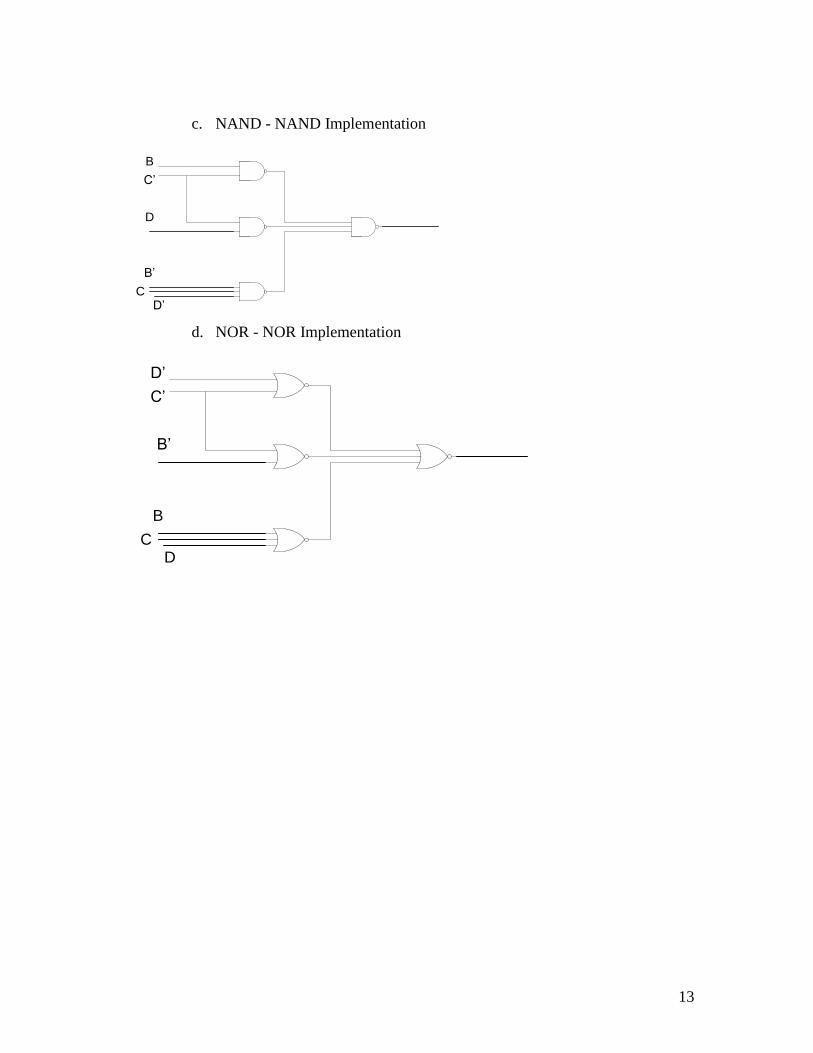
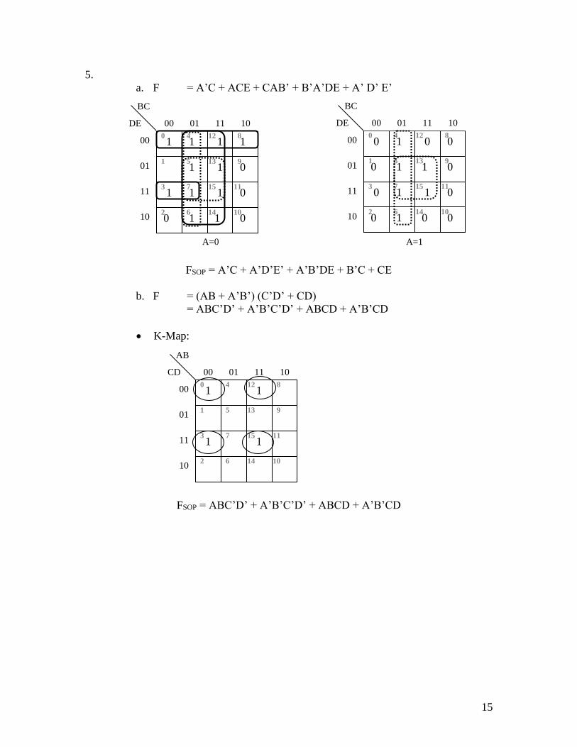
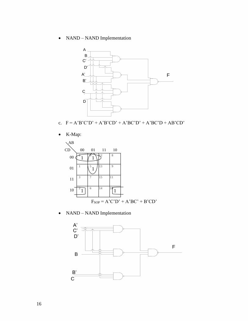
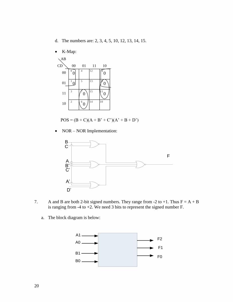
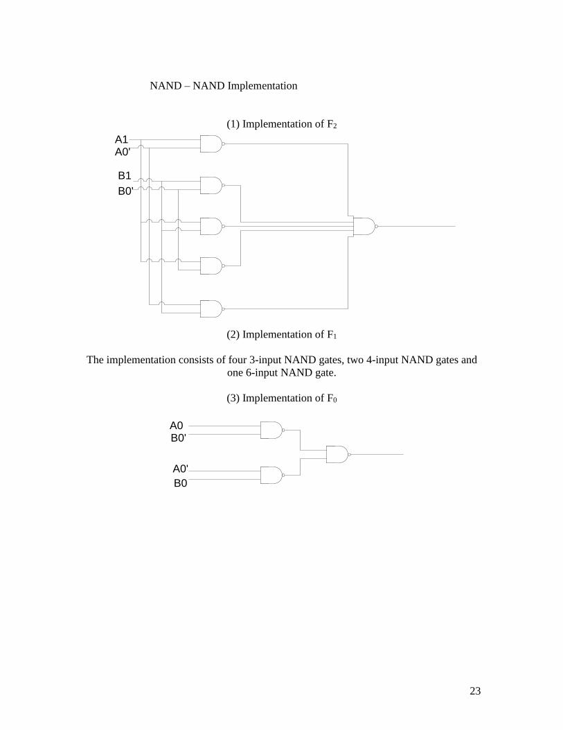
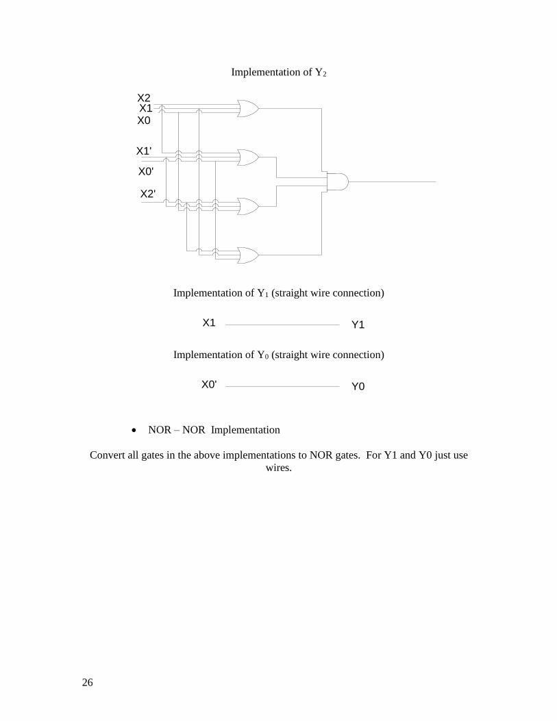
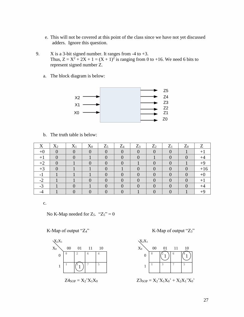

28
K-Map of output ldquoZ2rdquo K-Map of output ldquoZ0rdquo
Z2SOP = X2rsquoX1rsquoX0 Z0SOP = X2rsquoX0rsquo + X1rsquoX0rsquo
Note Z1 = 0 (constant)
0
1
6 4
5 7 3 1
00 01 11 10
0
1
2
X2X1
X0
1 0
1 1
6 4
5 7 3 1
00 01 11 10
0
1
2
X2X1
X0
29
10 Design a 1-bit comparator that takes in a bit X and a bit Y and outputs XltY
XgtY X=Y Use a single 2-to-4 decoder and 1 single OR gate
Consider the truth table of each of these simple functions We can implement
each as a sum of minterms And since a decoder implements the minterms of
the input variables we can arrive at the circuit above
X Y XltY XgtY X==Y
0 0 0 0 1
0 1 1 0 0
1 0 0 1 0
1 1 0 0 1
Y0
Y1
Y2
Y3
A0
A1
2-t
o-4
Decoder
X
Y XltY
XgtY
X=Y
30
HW5 - Signed Representations and Arithmetic
1
a
11 1
10100 = 20
+ 11101 = 29
Carry=1 110001 = 49
b
11100
- 10100
01000
28
- 20
8
1 1 1 1 _
11100
2rsquos comp 01011
+ 1
01000
2
b
1 1 1 1 _
101011
+ 011010
1000101
3 For unsigned subtraction we still use take the 2s complement of the bottom
number (but the check for overflow differs for unsigned vs 2s complement)
a 01101102 ndash 01001002 cannot be performed as is because we cannot
subtract a larger number from a smaller number in unsigned
representation
0110110
- 0100100
+54
-60
-6
1 1 1 1 1 1 _
0110110
2rsquos comp 1011011
+ 1
0010010
4
a Unsigned binary 28 lt 28310 lt 29 Therefore 9 bits 28310 = 1000110112
b 2rsquos complement with n-bits we can make ndash(2n-1) to +(2n-1-1) With n = 9
the range is -256 to +256 With n = 10 the range is -512 to +511 Thus
10 bits 28310 = 1000110112
5 Consider the following decimal numbers +21 +55 +121 -32 -99 -128
a What are the corresponding 8-bit signed-magnitude representation
31
a What are the corresponding 8-bit 2s complement representation
b Which of the above numbers can be represented in 6-bit signed-
magnitude 6-bit 1s complement 6-bit 2s complement representations
explain
21 55 121 -32 -99 -128 A 16+4+1=21
00010101 00110111 01111001 10100000 11100011 NA
B 00010101 00110111 01111001 1110000 10011101 10000000 C YYY
010101 in all cases
NNN NNN NNY 100000 in 2rsquos comp
NNN NNN
6 What are the corresponding decimal representations for the following binary
numbers 01011011 11010010 if
a The binary numbers are in 8-bit signed-magnitude format
b The binary numbers are in 8-bit 2s complement format
01011011 11010010 a) 64+16+8+2+1=91 -(64+16+2)=-82 b) 64+16+8+2+1=91 -128+64+16+2=-46
7 Perform the following addition problems for the following 2rsquos complement
numbers State whether overflow does or does not occur for each problem
Justify your answer for why overflow does or does not occur Check your
work by converting each number to decimal
a 1010 0111 b 1001 0110 c 0101 1100 d 0101 1101
+1110 0100 +1011 0011 +1011 0101 +0110 1001
11000 1011 10100 1001 10001 0001 1100 0110
n+n=n
cin=cout=1
No Overflow
n+n=p
cin=0cout=1
Overflow
p+n=p
cin=cout=1
NoOverflow
p+p=n
cin=1cout=0
Overflow
8 This is an exercise to help you remember what gates are used to create a full
adder Using a full adder as shown below and no other gates can you
produce the function Z = AbullB (Hint Write out the logical equations for S
and Cout and see if you can hook up the inputs to produce Z)
ANSWER
Cin X Y S Cout
0 0 0 0 0
32
0 0 1 1 0
0 1 0 1 0
0 1 1 0 1
1 0 0 1 0
1 0 1 0 1
1 1 0 0 1
1 1 1 1 1
S X Y Cin
Cout XY XCin YCin
=
= + +
We want Z=XY and if we set Cin=0 then the formulas of S and Cout
becomes as follows
S X Y
Cout XY
=
=
Thus Cout = Z = XY
X Y
S
CinFull Adder
Cout
A B
0Z
33
9 Using 1 half-adder and a minimal number of 4-bit binary adders design a
circuit to calculate Y = 25X where X is a 4-bit inputs
ANSWER
If a number is multiplied by a number that is a power of 2 then the number rewritten
using the above formula
2 00
n
n X X=
Y = 25X = 16X + 8X + X = X0000+X000+X
Also adding the information that X is a 4-bit number above formula can be re-written
X = X3X2X1X0
Y = X3X2X1X00000 + X3X2X1X0000 + X3X2X1X0
This can be written as addition by 4 bit adders
X3 X2 X1 X0
X3 X2 X1 X0 0 0 0
+ X3 X2 X1 X0 0 0 0 0
Since one row in each addition is all zeros they can be eliminated and the other two
numbers can be added using a 4-bit adder However the lower bits require only a single
bit adder The carry from the first addition is transferred to the next one
B3 B2 B1 B0 A3 A2 A1 A0
S0S1S2S3
C0C4 4-bit Binary Adder
X Y
S
Half AdderCout
X3 X0X0X1X2X3 X1X2X30 X0X1X2
Y8 Y7 Y6 Y5 Y4 Y3 Y0Y1Y2
34
10 Using a minimal number of 4-bit adders design a circuit that implements
Y=20X+107 where X is a 3-bit unsigned number
ANSWER
X = X2X1X0 and thus 20X= 16X+4X These numbers are achieved by inserting zeros
at the end Once we add these there numbers we see that not all bits require addition We
actually need only a single 4-bit adder and nothing more
1 1 0 1 0 1 1
X2 X1 X0 0 0
+ X2 X1 X0 0 0 0 0
Which can be collapsed to the following addition
1 1 X2 X1 X0 0 0
+ X2 X1 X0 1 0 1 1
B3 B2 B1 B0 A3 A2 A1 A0
S0S1S2S3
C0C4 4-bit Binary Adder
X0X1X2 X1X211
11
X0
Y7 Y6 Y5 Y4 Y3 Y0Y1Y2
0
1
35
11 Design a minimal circuit using ANDORNOT gates to implement the
comparison A gt 10 where A is a 4-bit number
a Start by writing out the logical algorithm for when A gt 10 then implement it
using gates
b Check that your work is minimal by using a K-Map
ANSWER
Letrsquos assume that the number A = A3A2A1A0
Logical Algorithm For any number A to be greater than a number B (in this case 1010 =
10102) a more significant bit of A must be greater than B However in the case of A
compared with 1010 we realize A3 and A1 can never be greater than the 1rsquos in those
places for 10 Similarly A2 and A0 can never be less than the 0rsquos in those places Thus
for A gt 10 there are only 2 cases that need to be checked
A3 = 1 and A2 gt 0 (ie A2 = 1)
OR
A3=1 and A1 = 1 and A0 gt 0 (ie A0 = 1)
Thus Agt10 = A3A2 + A3A2A0
Note that we donrsquot have to check A2 in the second case because it is DEFINITELY
greater than or equal to the 0 in that place of 10102
A K-Map will also show the same equation
SUM(1112131415)
Agt10=A3A2+ A3A1A0
A3
A2
A3
A0A1
Agt10
1
1
1
0
1
1
3
12 8
9 13 5 1
00 01 11 10
00
01
2 6
7 15
14 10
11
4
11
10
A3A2
A1A0
36
HW 6 ndash Latches and Flip-Flops
1 Complete the following waveforms for negative edge-triggered D Flip-Flops
D Q
QCK
D Q
QCK
CLK
D1
D2D1
D2
Z
X
CLK
X
D1
D2
Z
2 We should find the state diagram following the steps in the class notes
a Convert the diagram to a table
Current
State
Next State Output
XY= 00 XY= 01 XY= 10 XY= 11
Q1 Q0 Q1 Q0
Q1
Q0 Q1
Q0 Q1
Q0 Z
0 0 0 0 0 0 1 0 1 0 0
0 1 0 0 0 0 0 1 0 1 1
1 0 0 0 0 1 0 0 0 1 0
1 1 0 0 0 1 0 1 0 1 0
37
Convert Q to D
Current
State
Next State Output
XY= 00 XY= 01 XY= 10 XY= 11
Q1 Q0 D1 D0 D1 D0 D1 D0 D1 D0 Z
0 0 0 0 0 0 1 0 1 0 0
0 1 0 0 0 0 0 1 0 1 1
1 0 0 0 0 1 0 0 0 1 0
1 1 0 0 0 1 0 1 0 1 0
b Perform K-maps to find equations for D1 and D0
D0 = Q1Y + Q0X
D1 = Q1rsquoQ0rsquoX
c Draw the circuit and implement the initial state (reset) condition
D Q
QCK
D Q
QCK
ZX
Clock
Q0
Q1Y
PRE PRE
CLR CLR
Reset Reset
GND GND
38
3 Because we have 2 states in the state diagram we use one D flip-flop to
implement state memory We design the combinational logic for the next-state
logic and the output function logic by building up the statetransition table
Current State Next State Output
XY = 00 XY = 01 XY = 10 XY = 11
SymbolCode SymbolCode SymbolCode SymbolCode SymbolCode H
F 0 F 0 G 1 G 1 G 1 0
G 1 F 0 F 0 F 0 G 1 1 Q0(t) Q0
D0 Q0
D0 Q0
D0 Q0
D0
After we get the statetransition table we build the K-Maps to simplify expressions for
D0 and H
bull D0 K-Map
D0 = YQ0rsquo + XQ0rsquo + XY H = Q0
0
1 1 1
1
6 4
5 7 3 1
00 01 11 10
0
1
2
XY
Q0
39
4
Current State Next State amp Flop-Flop Inputs Outputs
Next State Next State
X = 0 X = 1
SymbolCode SymbolCode SymbolCode Z
A00 B01 D11 0
B01 C10 B01 0
C10 B01 A00 1
D11 B01 C10 0 Q1(t)Q0(t) Q1(t+1)Q0(t+1) Q1(t+1)Q0(t+1)
After we get the statetransition table we build the K-Maps to simplify expressions for
D1 D0 and Z
bull D1 K-Map D0 K-Map
D1 = XrsquoQ1Q0 + XQ0rsquo D0 = XrsquoQ1+XQ0 + XQ1rsquo
Z K-Map
Z = Q1Q0rsquo
1
1 0
0 1
1 0
1 00
01
11
10
0 Q1Q0
X
1
1
0 0
1 0
0 1
0 00
01
11
10
0 Q1Q0
X
1
1
0 0
0 0
1
0 Q0
Q1
1
40
a The waveform is below
CLK
X
Q1
Q0
State
Z
A D B C A B
41
5
a We need 4 states and each of them stores one 2-bit binary number ranging
from 00 to 11
State S0 S1 S2 S3
Assignment
(Q1 Q0)
00 01 10 11
The state diagram is below
b Because we have 4 states in the state diagram we use two D flip-flops to
implement state memory We design the combinational logic for the next-
state logic and the output function logic by building up the statetransition
table
U ndash UP D ndash DOWN
Current State Next State
UD = 00 UD = 01 UD = 10 UD = 11
SymbolCode SymbolCode SymbolCode SymbolCode SymbolCode
S000 S000 S311 S101 S000
S101 S101 S000 S210 S101
S210 S210 S101 S311 S210
S311 S311 S210 S000 S311 Q1(t)Q0(t) Q1(t+1)Q0(t+1)
D1D0 Q1(t+1)Q0(t+1)
D1D0 Q1(t+1)Q0(t+1)
D1D0 Q1(t+1)Q0(t+1)
D1D0
After we get the statetransition table we build the K-Maps to simplify expressions for
D1 and D0
S0 S1 S2 S3
UP=DOWN=1 or
UP=DOWN=0
UP=DOWN=1 or
UP=DOWN=0
UP=DOWN=1 or
UP=DOWN=0UP=DOWN=1 or
UP=DOWN=0
UP=1 and
DOWN=0
UP=1 and
DOWN=0UP=1 and
DOWN=0
UP=1 and DOWN=0
UP=0 and
DOWN=1UP=0 and
DOWN=1
UP=0 and
DOWN=1
UP=0 and DOWN=1
~R
ese
t
42
bull D1 K-Map
D1 = UrsquoDrsquoQ1 + DQ1Q0 + UQ1Q0rsquo + UrsquoDQ1rsquoQ0rsquo + UDrsquoQ1rsquoQ0
bull D0 K-Map
D0 = UrsquoDrsquoQ0 + UDQ0 + UrsquoDQ0rsquo + UDrsquoQ0rsquo
c The waveform is below
CLK
UP
DOWN
Q1
Q0
1
1
1
1
1
1
0
1
1
3
12 8
9 13 5 1
00 01 11 10
00
01
2 6
7 15
14 10
11
4
11
10
UD
Q1Q0
1
1
1
1
0
1 1
1 1
3
12 8
9 13 5 1
00 01 11 10
00
01
2 6
7 15
14 10
11
4
11
10
UD
Q1Q0
43
6 Complete the waveform for the 4-bit counter presented in class
1111
Clock
SR
CEP
CET
PE
P3-P0
Q3-Q0 1101
1101
1110 0000 0001 0000 1110 1111
7 Complete the waveform for a 4-bit D-Register with Data (Load) Enable and
asynchronous reset
CLK
AR
EN
0110D[30] 0001 10111010 11011001 10001111 0111
Q[30] 1010 11111101 10000000 1011
44
81 Unit 7 ndash Datapath Design 1 Implement a circuit that takes in a 4-bit number X[30] and produces a 4-bit value
Z[30] according to the following function
if X lt 8 then
Z = X + 5
else
Z = X ndash 2
Using the building blocks below and at most 1 inverter (no other gates)
implement this function
Note To check Xlt8 subtract X-8 by taking the 2rsquos complement of 8 The 2rsquos comp of
8 is 0111+1 Recall a carry of 0 when subtracting unsigned numbers (A-B) indicates
overflow which can only occur in unsigned subtraction if the result needed to be negative
(ie A lt B) So C4 will only be 1 if X is not less-than 8 We can invert it to get a signal
that is true when X lt 8 Use those signals to either add 5 (0101) or subtract 2 (add 1110)
B3 B2 B1 B0 A3 A2 A1 A0
S0S1S2S3
C0C4 4-bit Binary Adder
X lt 8
Xlt8
X0X1X2X3
Z0Z1Z2Z3
B3
B2
B1
B0
A3
A2
A1
A0
S0
S1
S2
S3
C0
C4
4-b
it B
inary
Add
er
X3
X2
X1
X0
1
1
1
0
1
0
1
45
2 Design a circuit that takes in an 4-bit number X[30] and outputs a number Y and
performs the operation below Assume these numbers are unsigned Use a 4-bit
adder and 2-to-1 muxes Hint Multiplying by 4 (ie 22) in binary can be done with
no gates just as multiplying by 100 (ie 102) in decimal can be done simply and
easily
if(X lt 00112)
Y = 4X
else
Y = X
4X would require 6 outputs and be X3 X2 X1 X0 0 0 thus even if we pass X we need to
produce 6 outputs Recall subtracting 3=0011 bin is the same as adding the 2s
complement Next a carry of 0 when subtracting unsigned numbers (A-B) indicates
overflow which can only occur in unsigned subtraction if the result needed to be negative
(ie A lt B)
I1
Y
S
I0
I1
Y
S
I0
I1
Y
S
I0
I1
Y
S
I0
I1
Y
S
I0
I1
Y
S
I0
X0
X1
X2
X3
0
0
0
0
X0
X1
X2
X3
Y5
Y4
Y3
Y2
Y0
Y1
X lt 3
B3
B2
B1
B0
A3
A2
A1
A0
S0
S1
S2
S3
C0
C4
4-b
it B
inary
Add
er
X3
X2
X1
X0
0
0
1
1
1
46
3 Design a circuit that takes in two 4-bit numbers X[30] and Y[30] along with two
function select bits FS1 and FS0 and produces an output Z[30] according to the
following table
FS1FS0 Z
00 X+Y
01 X-Y
10 Y-X
11 donrsquot care
Use (1) 4-bit adder 4-bit wide 2-to-1 muxes and any basic gates you desire
Approach Take a 4-bit adder and for each operation listed in the table above
identify what should be passed to the A and B inputs of the adder Then use
muxes to perform that function Design logic for the select bits of the muxes and
the carry-in of the adder that use FS1 and FS0 as input
Note In the solution below the A and B inputs of the muxes are like the 0th and
1st inputs of 4 2-to-1 muxes respectively Ignore the G input
B3
B2
B1
B0
A3
A2
A1
A0
S3
S2
S1
S0
C0
C4
S
G
1A
1Y
2Y
2-to-1
4-bit
wide
mux
2A
3A
4A3Y
4Y1B
2B
3B
4B
0
S
G
1A
1Y
2Y
2-to-1
4-bit
wide
mux
2A
3A
4A3Y
4Y1B
2B
3B
4B
0
X3
X2
X1
X0
X3
X2
X1
X0
Y3
Y2
Y1
Y0
Y3
Y2
Y1
Y0
Z3
Z2
Z1
Z0
FS1
FS0
FS1FS0
74LS
283
47
4 Design a circuit that takes in two 4-bit signed magnitude numbers X[30] and
Y[30] and produces two 4-bit outputs A[30] and B[30] according to the following
algorithm
if X gt= Y then
A = X and B = Y
else
A = Y and B = X
Use a 4-bit adder to subtract and perform the comparison 4-bit wide 2-to-1
muxes and basic logic gates Assume the input 1000 = -0 will never occur on X
or Y
Approach First think about how to compare signed magnitude numbers by using
unsigned comparison techniques and how to precondition the inputs to allow the
use of unsigned comparison For example 1001 = -1 in signed magnitude and
0100 = +4 in signed magnitude So 1001 is really less than 0100 Use the
comparison result to control the selects of the muxes
Y0
Y1
Y2
Y3
X0
X1
X2
X3
XgtY
S
G
1A
1Y
2Y
2-to-1
4-bit
wide
mux
2A
3A
4A3Y
4Y1B
2B
3B
4B
0
S
G
1A
1Y
2Y
2-to-1
4-bit
wide
mux
2A
3A
4A3Y
4Y1B
2B
3B
4B
0
X3
X2
X1
X0
Y3
Y2
Y1
Y0
X3
X2
X1
X0
Y3
Y2
Y1
Y0
A3
A2
A1
A0
B3
B2
B1
B0
B3
B2
B1
B0
A3
A2
A1
A0
S0
S1
S2
S3
C0
C4
4-b
it B
inary
Add
er
1
48
5 Design a circuit that adds two 4-bit unsigned numbers X[30] and Y[30] and
outputs either the sum if there is no overflow or 1111 (=1510 the maximum unsigned
4-bit number) if there is overflow
Unsigned overflow is found by looking at Cout You could use a mux to select the sum
or 1111 but realize you can just use OR gates for this function
B3
B2
B1
B0
A3
A2
A1
A0
S3
S2
S1
S0
C0
C4
74LS
283
X3
X2
X1
X0
UNS_OV
0
Y3
Y2
Y1
Y0
G0
G1
G2
G3
49
1 We would like to build an adder whose inputs are in units of pennies and produces
sum in nickels and pennies Essentially this is a base-5 adder The 2 inputs of this
adder are A=A2A1A0 and B=B2B1B0 Assume that the maximum input number
that A and B can be is 4 pennies Design an adder to produce the correct
nickelspennies sum C= [CN] [CP2CP1CP0] To implement this design you may
assume you can use as many 4-bit adders as you like
if X+Y gt 4 dec then
CN = 1 CP[20] = X+Y-5
else
CN = 0 CP[20] = X+Y
A2 A1 A0 B2 B1 B0
CP2 CP1 CP0
To be designed by you
CN
Block diagram for the
nickelpenny adder you
are going to design
50
B3 B2 B1 B0 A3 A2 A1 A0
S0S1S2S3
C0C4 4-bit Binary Adder
Z4 Z2 Z1
CP2
0
0
B3 B2 B1 B0 A3 A2 A1 A0
S0S1S2S3
C0C4 4-bit Binary Adder
0 X4 X2 X1 0 Y4 Y2 Y1
Z8 Z4 Z2 Z1
0
B3 B2 B1 B0 A3 A2 A1 A0
S0S1S2S3
C0C4 4-bit Binary Adder
0 1 0 0 Z8 Z4 Z2 Z1
1
Need actual
inverters here
just didn t
draw them
CN
(4 lt X+Y)
CP1 CP0
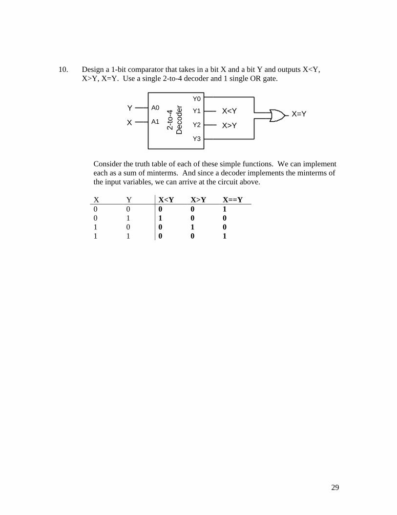
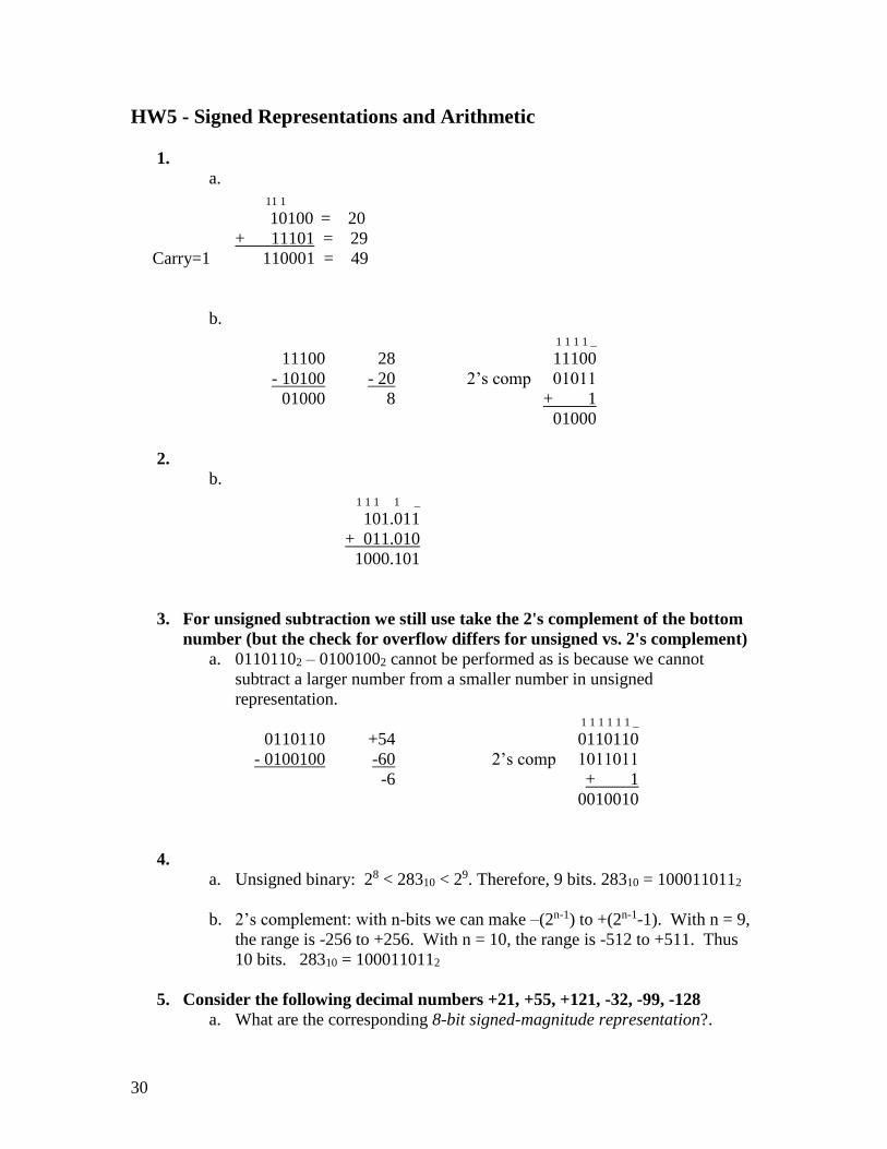
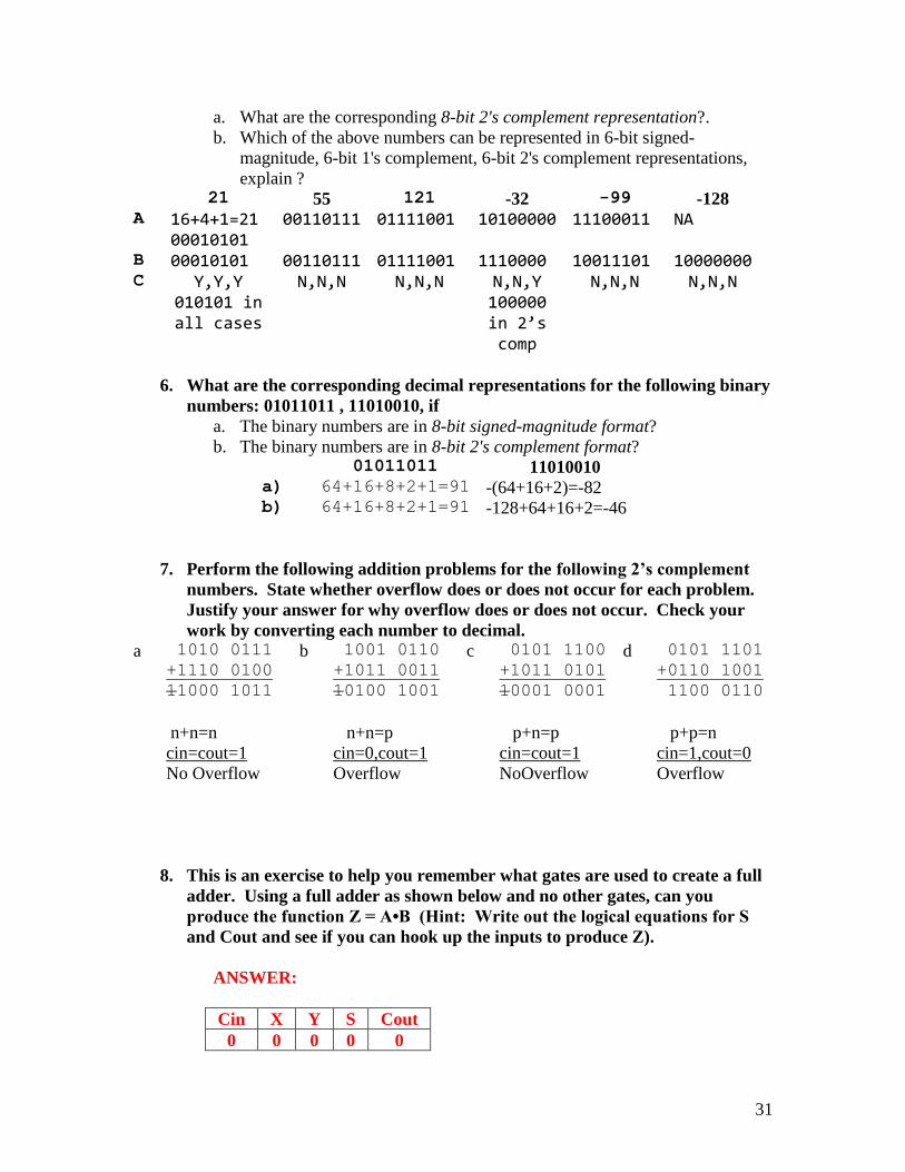
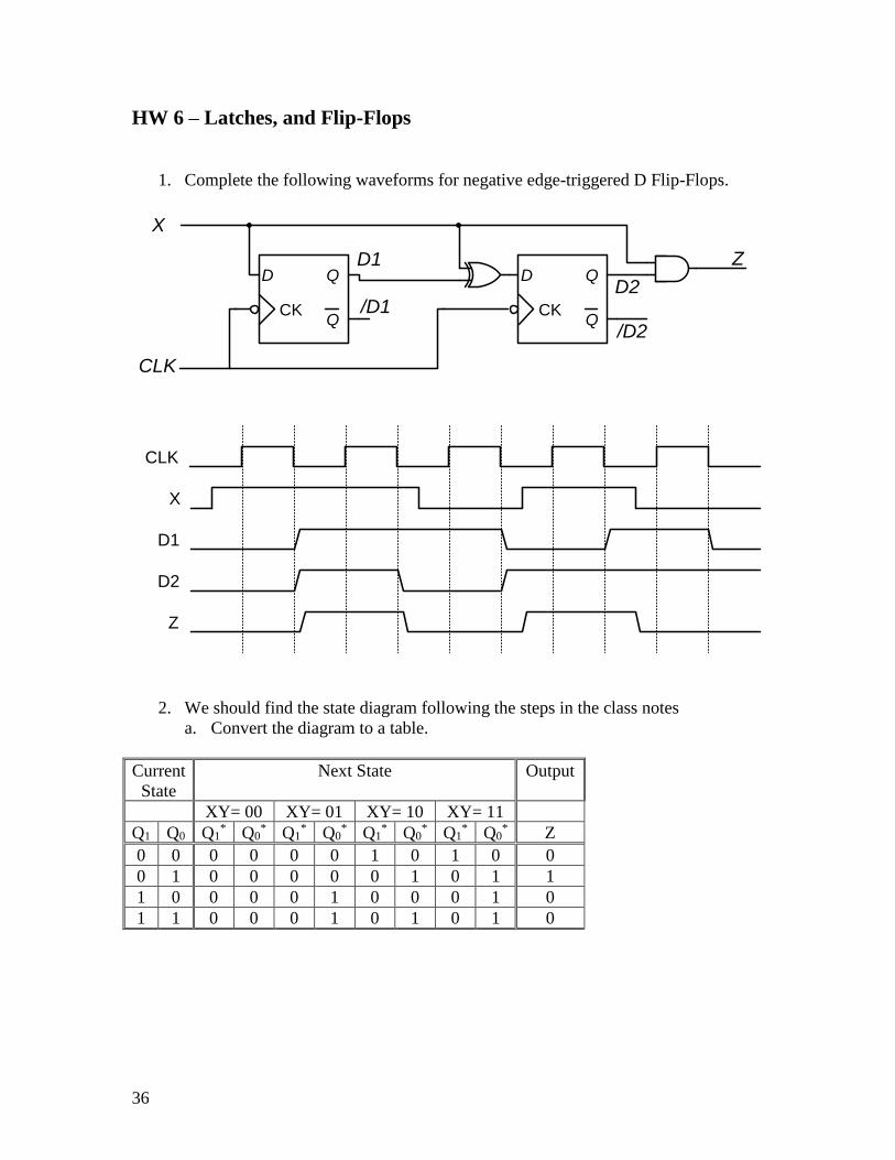
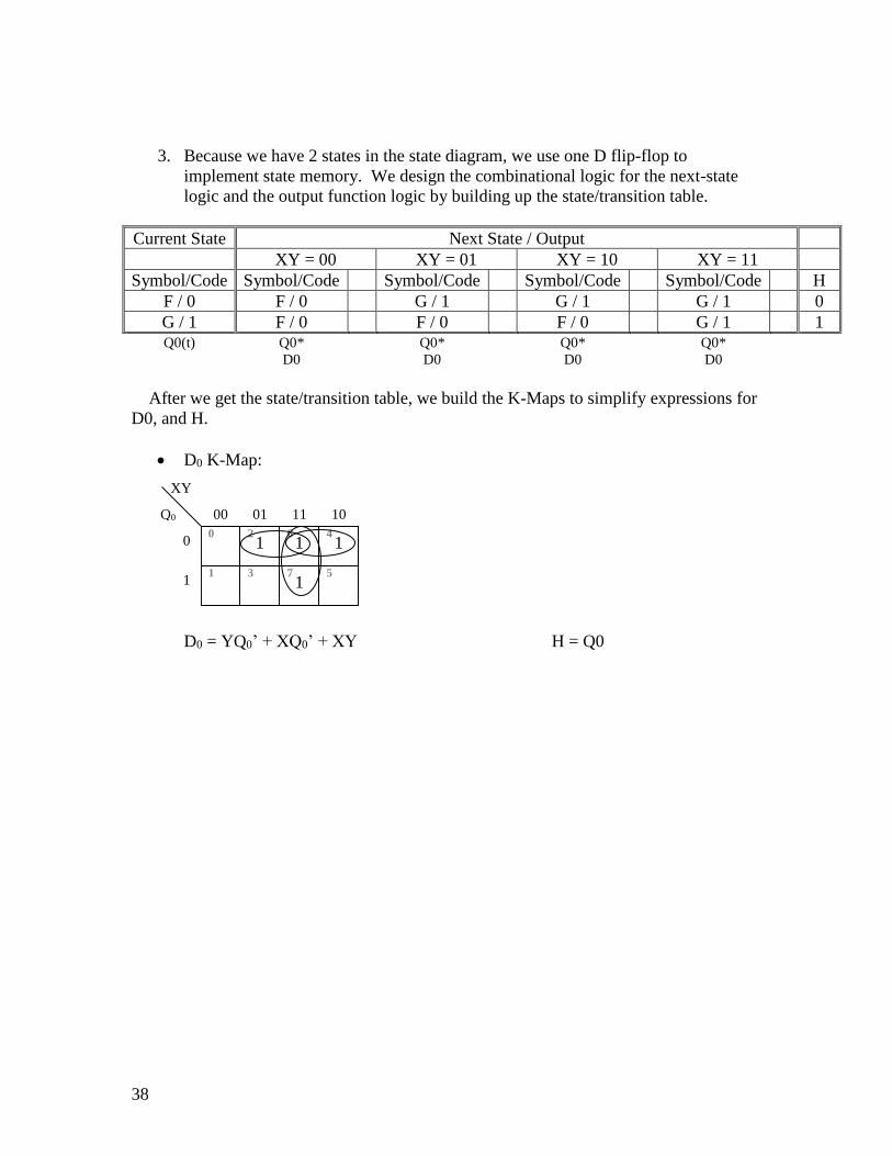
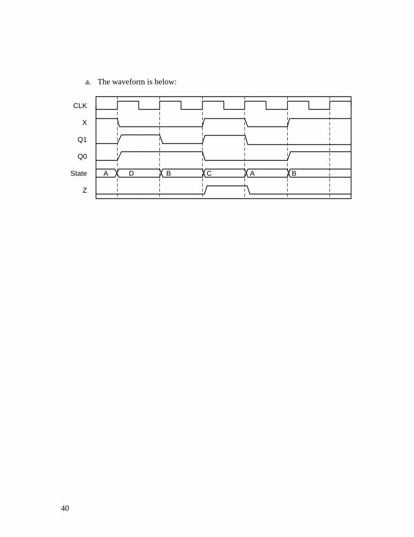
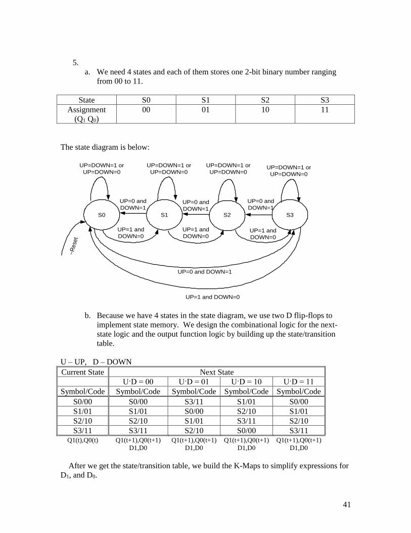
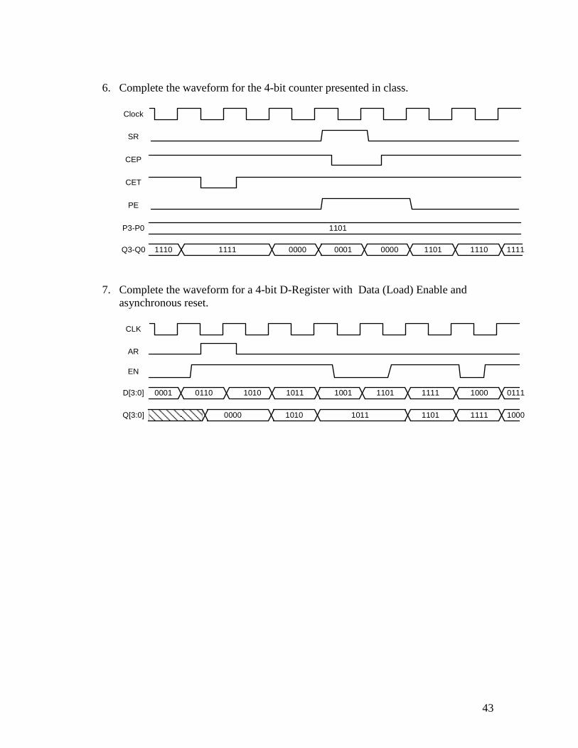
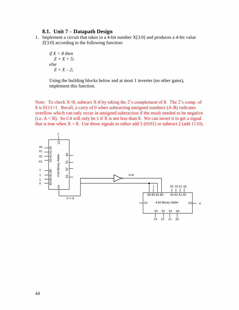
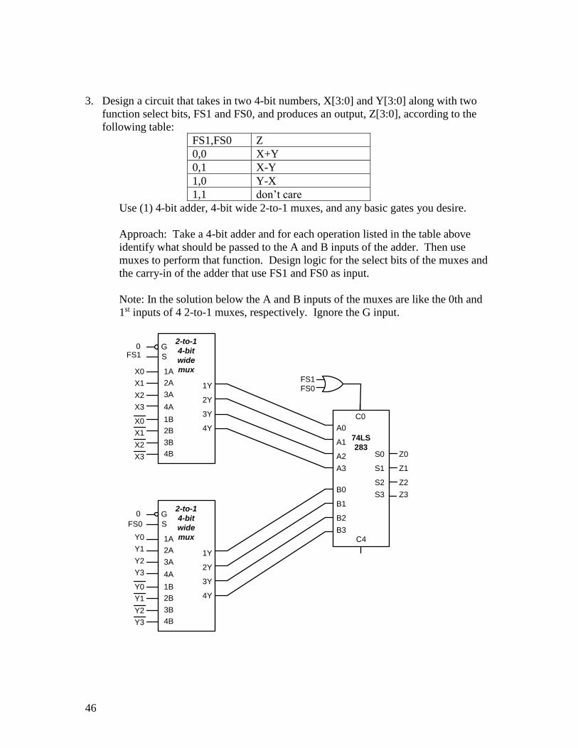