ee16.468/16.568lecture 7electro-optical integrated circuits principles of cdma
TRANSCRIPT

EE16.468/16.568 Lecture 7Electro-optical Integrated Circuits
Principles of CDMA

EE16.468/16.568 Lecture 7Electro-optical Integrated Circuits
Optical CDMA advantages:
• Perform signal encoding/decoding in optical domain directly – potentially high speed (>100Gbit/s).
• Avoid electrical/optical and optical/electrical conversion bottleneck.
• Efficient bandwidth utilization.
• Data format and protocol transparent – simplified architecture and network maintenance.
• Simplified network architecture, less equipment inventory, flexible, scalable network.

EE16.468/16.568 Lecture 7Electro-optical Integrated Circuits
Fiber to the home (FTTH)

EE16.468/16.568 Lecture 7Electro-optical Integrated Circuits
Challenges:
• Accurate and tunable phase control
• All-optical switch and amplitude modulation
• Integrated circuits with these functionalities
Polymeric waveguide based photonic circuits:
• Large electro-optic (EO) and Thermo-Optic coefficients: - polymer TO ~ -1.4 x 10⁻⁴/°C; silica, T.O. ~ 1 x 10⁻⁵/°C - Polymer EO ~ 80pm/V, LiNbO3 ~ 33pm/V
• Low dielectric constant -- Potentially high–speed operation: - polymer: r ~ 2.3, Si: r ~ 10 - Capacitance ~ 5 times smaller than Si based circuits.

EE16.468/16.568 Lecture 7Electro-optical Integrated Circuits
• Multifunction capability --- Photonic integrated circuits
Polymeric waveguide based photonic circuits:
• Flexible substrate, low cost and relative simple fabrications
4
1, 2, 3
filter
Electro-optic SSB modulator
AmplifierEO phase shifter
Si Electronics

EE16.468/16.568 Lecture 7Electro-optical Integrated Circuits
Fiber to the home (FTTH)

EE16.468/16.568 Lecture 7Electro-optical Integrated Circuits
Polymeric waveguide based OCDMA decoder

EE16.468/16.568 Lecture 7Electro-optical Integrated Circuits
Received signal SNR
• High bit error rate (BER) due to correction noise.• Need long sequence to reduce the correction error.

EE16.468/16.568 Lecture 7Electro-optical Integrated Circuits
Orthogonal Amplitude-phase Coding
),()()(
)()()(
,
1
0
1
0
kicc
N
m
km
N
n
in
ki
nTtumTtubb
tXtXR
EE16.468/16.568 Lecture 7Electro-optical Integrated Circuits
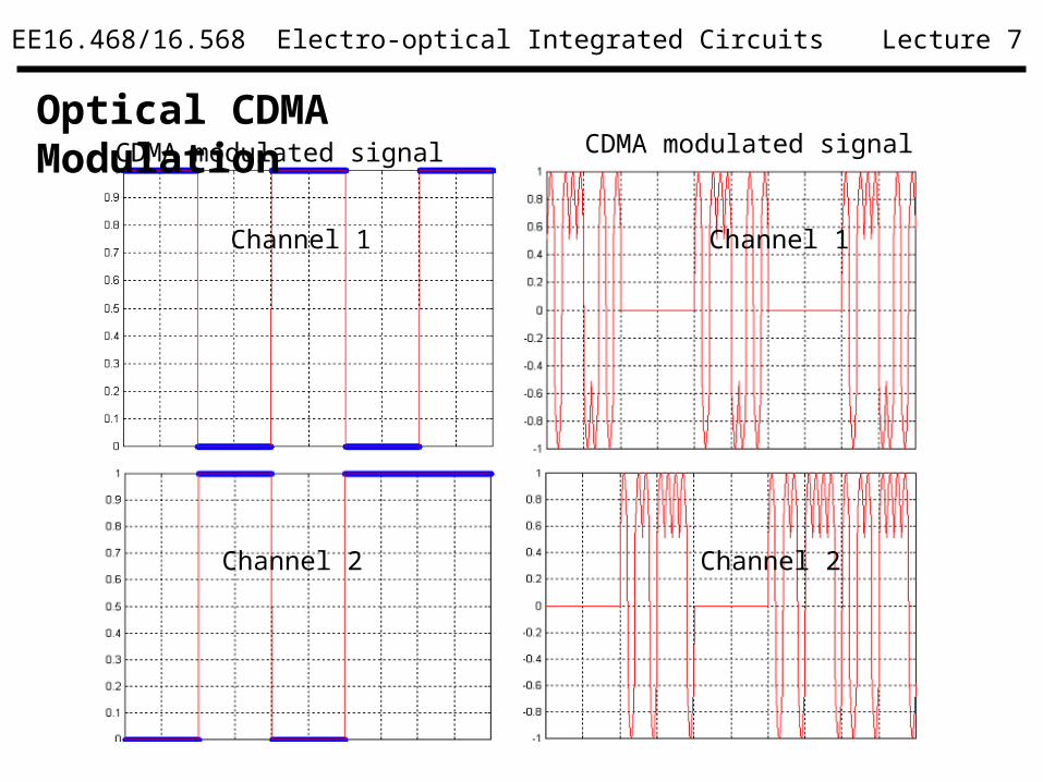
Optical CDMA Modulation
Channel 1
Channel 2
CDMA modulated signal
Channel 1
Channel 2
CDMA modulated signal

EE16.468/16.568 Lecture 7Electro-optical Integrated Circuits
Received signal
Time scale 25ps/100units
CDMA demodulated channel 1 signal CDMA demodulated channel 2 signal

EE16.468/16.568 Lecture 7Electro-optical Integrated Circuits
Polymer Waveguide optical Time Gate

EE16.468/16.568 Lecture 7Electro-optical Integrated Circuits
100Gb/s Tranceivers
• High-speed (>40Gb/s) external modulators not available. • Extremely difficult to achieve CDR using high-bandwidth (>40GHz) electronic circuitry even with low k and scale VLSI technologies. • SNR degradation for ultra-high frequency circuitry.• Very expensive.
Difficulties of traditional transceivers

EE16.468/16.568 Lecture 7Electro-optical Integrated Circuits
100Gb/s All-optical Transceiver Interface Module
1. Interface the relative slow electronics circuit.2. Perform pulse reshape and retiming without OE-EO
conversion.3. Future all-optical packet routing.
Why All-optical Module
Challenges:
1. 100GHz optical clock generation.2. Optical threshold gate.3. Re-shaping and re-timing.

EE16.468/16.568 Lecture 7Electro-optical Integrated Circuits
Architecture of 100Gb/s Transceiver Interface Module
• Precisely controlled time delays
• Photonics integrated circuit approach

EE16.468/16.568 Lecture 7Electro-optical Integrated Circuits
Architecture of 100Gb/s Transceiver Module
Pulse compressor:
0
0.005
0.01
0.015
0.02
0.025
0.03
0 0.1 0.2 0.3 0.4 0.5 0.6 0.7Normalized input light intensity
Ref
ract
ive
inde
x ch
ange
Normal Kerr Effect
Dispersive Bragg gratingenhanced Kerr effect

EE16.468/16.568 Lecture 7Electro-optical Integrated Circuits
Kerr Nonlinearity in Semiconductors
Wcmn /103~ 2142
Kerr Nonlinearity:,2
2 InIKEn
in InP semiconductor
• Index change and tuning range:
• For high index contrast (3.5:1), 10mW laser power induces index changes of 0.03.
• Pulse compression ratio >10.
1295 1296 1297 1298 1299 1300 1301 1302 1303 1304 13050
0.1
0.2
0.3
0.4
0.5
0.6
0.7
0.8
0.9
1
wavelength nm
refle
ctio
n %

EE16.468/16.568 Lecture 7Electro-optical Integrated Circuits
Architecture of 100Gb/s Transceiver Module
DeMux:
EE16.468/16.568 Lecture 7Electro-optical Integrated Circuits
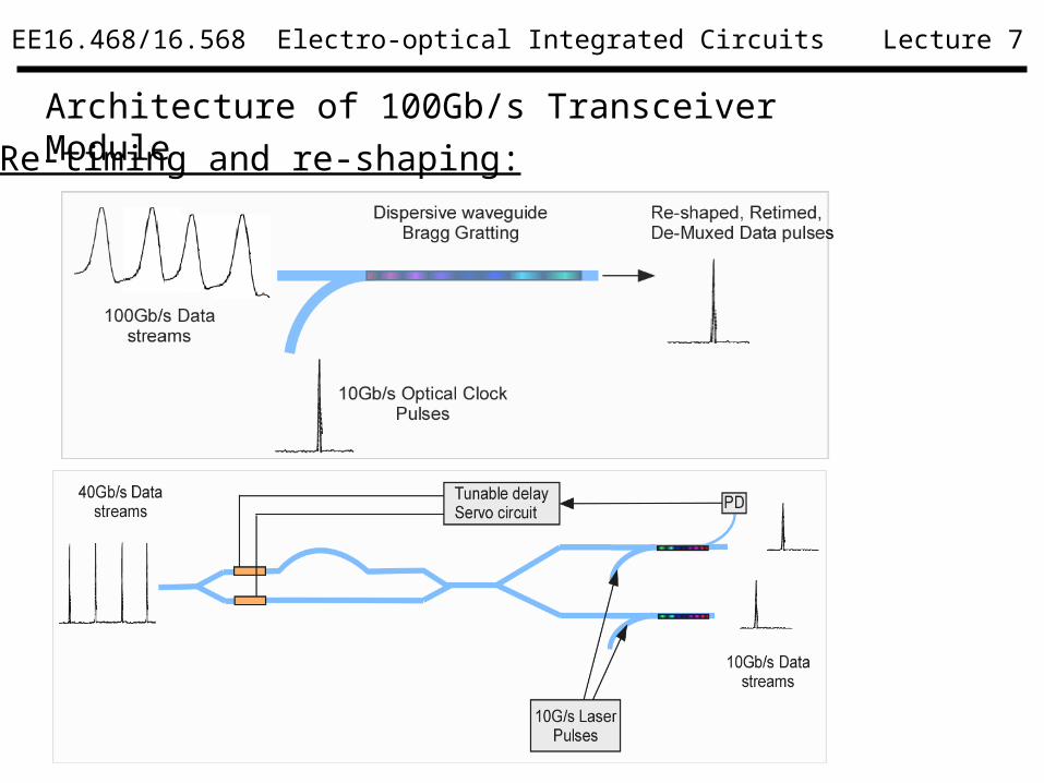
Architecture of 100Gb/s Transceiver Module
Re-timing and re-shaping:

EE16.468/16.568 Lecture 7Electro-optical Integrated Circuits
Other possible application – Optical Threshold Gates

EE16.468/16.568 Lecture 7Electro-optical Integrated Circuits
Optical phase corruption
EE16.468/16.568 Lecture 7Electro-optical Integrated Circuits
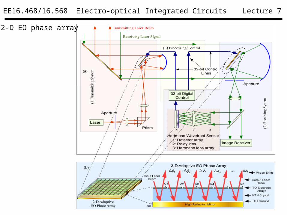
2-D EO phase array