ee452 senior capstone project: integrationofmatlab...
TRANSCRIPT
EE452 Senior Capstone Project:
Integration of Matlab Tools for DSP Code Generation
Kwadwo Boateng Charles Badu
May 8, 2006
Bradley University College of Engineering and Technology
Electrical and Computer Engineering Department Dr. Thomas Stewart, Professor
Boateng, Badu
2
2
Summary This document covers the design of communication systems based on discrete and
continuous-time (AM, FSK, DSB-SC, QAM, BPSK) modulation schemes. Matlab tools and
Code Composer Studio 3.1 software package are integrated to generate code for each
communication system. This generated code is implemented on the Texas Instrument DSP
board (TMSC6713). The design of each communication system is covered in detail. Any
problems encountered are explained, possible solutions are given, and expected results are
stated. An application of each communication system is discussed and a possible solution to
problems of each communication system is also addressed.
Boateng, Badu
3
3
Table of Contents Summary……………….. …………………………………………………….. 2 Table of Contents .......................................................................................................... 3 Introduction .................................................................................................................. 4 Design Overview ……………………………………………………………... 5 Digital Filters ……………………………………………………………... 5 FIR filter Implementation (Notch Filter)……………………………………….5 Notch Filter experimental results……………………………………………….7 Modulation Schemes………………………………………………………….. 8
Modulation……. …………………………………………………………..8 Specification………………………………………………………………...9
Amplitude Modulation (AM)..………………………………………………... 9 AM Transmitter…………………………………………………………... 10 AM Receiver……………………………………………………………… 11 AM Experimantal Results………………………………………………….13
Frequency Shift Keying (FSK)………………………………………………... 14 FSK Transmitter…………………………………………………………. 15 FSK Receiver…………………………………………………………….. 18 Analysis I………………………………………………………………… 20 FSK Experimental Data………………………………………………….. 21 Analysis II………………………………………………………………... 22
Double –Sideband Suppressed Carrier (DSB-SC)....…………………………... 23 DSB-SC Transmitter……………………………………………………... 23 DSB-SC Receiver………………………………………………………... 24 Analysis III………………………………………………………………. 26
Binary Phase-Shift Keying (BPSK)…………………………………………… 26 BPSK Receiver………………………………………………………….... 26 Analysis IV................................................................................................................... 28
Quadrature Amplitude Modulation (QAM)…………………………………… 28 QAM Modulator………………………………………………………….. 29 QAM Modulator experimental results…………………………………….. 32 QAM Demodulator………………………………………………………. 34 QAM Demodulator experimental results………………………………….. 40 Capacitor Coupling…………………………………………………………… 40 Capacitor Coupling experimental results………………………………………. 43 Conclusion …………………………………………………………………… 43 Future Work…………………………………………………………………….43 Bibliography ……………………………………………………………………43
Boateng, Badu
4
4
I. Introduction The objective of this project is to integrate Matlab tools with Code Composer Studio 3.1
software package in order to generate C-code to be implemented on the Texas Instrument
DSP board (TMSC6713). This integration process will involve the design of digital filters
and communication systems based on both continuous and discrete-time modulating
schemes. The modulating schemes include: Amplitude Modulation (AM), Frequency-Shift
Keying (FSK), Binary Phase-Shift Keying (BPSK), Double Side Band-Suppressed Carrier
(DSB-SC) and Quadrature Amplitude Modulation (QAM). Each modulating scheme will be
designed and simulated in Simulink, an extension of Matlab, and verified experimentally on
an oscilloscope. Applications of these modulation schemes in industry will also be discussed.
Design blocks that may be unavailable in Simulink, will be coded in C-code and called as
subroutines using the Matlab embedded function as if they were built in functions. These
built-in functions are commonly referred to as MEX-Files (Matlab executable files). A user
manual will be an important outcome of this project.
Boateng, Badu
5
5
II. Design Overview
DIGITAL FILTERS
A digital filter is simply a discrete-time, discrete-amplitude convolver. A digital filter is better
conceptualized in the frequency domain. The frequency domain impulse response is then
transformed into a time domain impulse response which is converted to the coefficients of
the filter.
Digital filters are used for two general purposes:
� Separation of signals that have been combined,
� Restoration of signals that have been distorted in some way.
Two basic types of digital filters:
� Finite Impulse Response (FIR)
� Infinite Impulse Response (IIR)
FIR FILTER IMPLEMENTATION
NOTCH FILTER
Filter that passes most frequencies unaltered, but attenuates those in a narrow range to very
low levels. This method of band pass filter implementation is approached when a given
formula for H (Z) is given. Consider the H (Z) in equation (1)
H(Z) =h0+hz-1 + hz-2 Equation (1)
H (z) around the unit circle becomes the filter's frequency response H (j). This means that
substituting ej for z in H (z) gives us an expression for the filter's frequency response. The
band pass filter will have a transfer function as shown in equation 2.
(Z-ejpi/4)(Z-e-jpi/4)
H(z) = ---------------------- Equation (2)
Z2
Boateng, Badu
6
6
Using Euler’s identity, coefficients for the transfer function in Z transformation is gotten for
the numerator and denominator.
fa = fd*fs Equation (3)
From Equation (3) we can solve for the analog frequency (fa), knowing the digital frequency (fd) and varying the sample frequency (fs). As the FIR filter would be tested on the DSP board (fs) will be vary depending on the ranges of sampling frequencies used by the board. The FIR filter is implemented in mat-lab to check it works theoretically before implementing
on the DSP board.
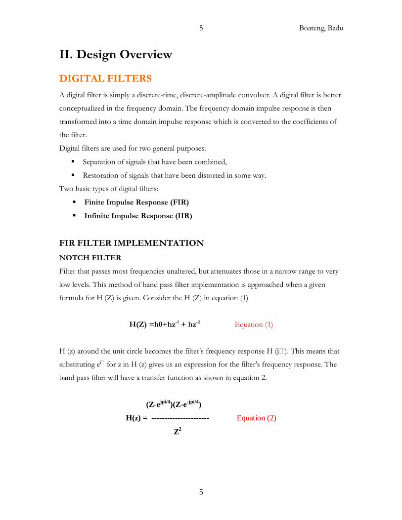
Figure 1-A: Frequency response of FIR filter
From figure 1-A, it can be noticed the response goes to zero at the point when fa is at a
1000(Hz). Blocks are generated in simulink to build our FIR filter to show the same
characteristics as shown in figure 1-B.
0 500 1000 1500 2000 2500 3000 3500 40000
0.5
1
1.5
2
2.5
3
3.5frequency response
Boateng, Badu
7
7
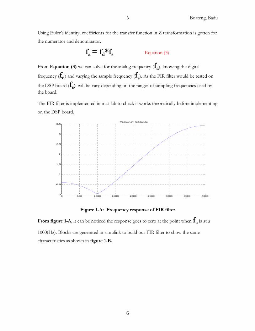
Figure 1-B: FIR implementation in simulink
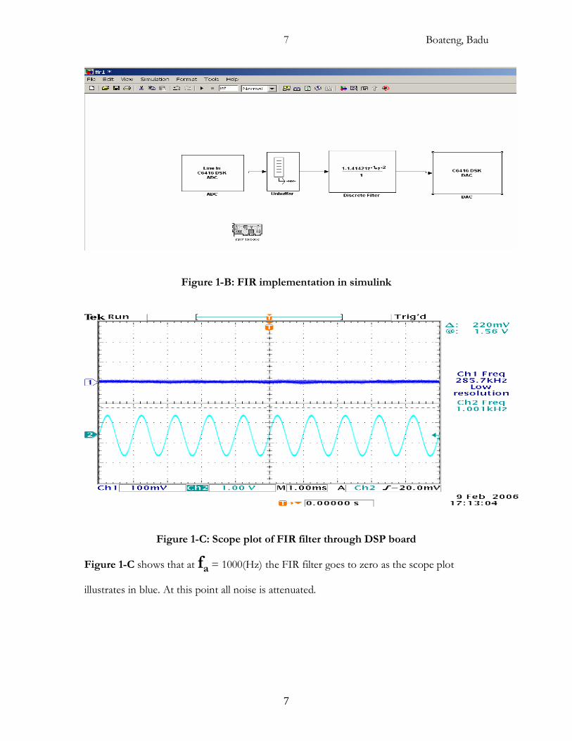
Figure 1-C: Scope plot of FIR filter through DSP board
Figure 1-C shows that at fa = 1000(Hz) the FIR filter goes to zero as the scope plot
illustrates in blue. At this point all noise is attenuated.
Boateng, Badu
8
8
III. MODULATION SCHEMES
Different aspects of modulation schemes in communication theory was researched, designed
and implemented in simulink.
Types of Modulation schemes
� Amplitude Modulation (AM)
� Frequency-shift keying (FSK)
� Double-sideband suppressed carrier (DSB-SC)
� Quadrature Amplitude Modulation (QAM)
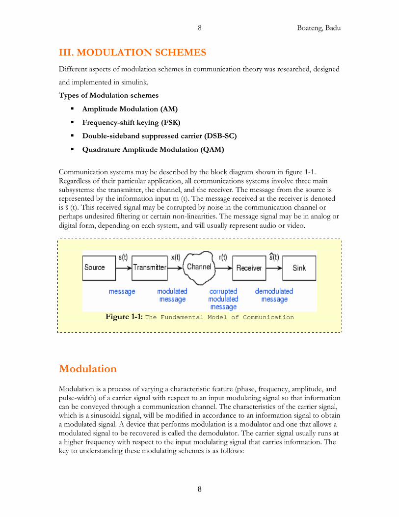
Communication systems may be described by the block diagram shown in figure 1-1. Regardless of their particular application, all communications systems involve three main subsystems: the transmitter, the channel, and the receiver. The message from the source is represented by the information input m (t). The message received at the receiver is denoted is ŝ (t). This received signal may be corrupted by noise in the communication channel or perhaps undesired filtering or certain non-linearities. The message signal may be in analog or digital form, depending on each system, and will usually represent audio or video.
Figure 1-1: The Fundamental Model of Communication
Modulation
Modulation is a process of varying a characteristic feature (phase, frequency, amplitude, and pulse-width) of a carrier signal with respect to an input modulating signal so that information can be conveyed through a communication channel. The characteristics of the carrier signal, which is a sinusoidal signal, will be modified in accordance to an information signal to obtain a modulated signal. A device that performs modulation is a modulator and one that allows a modulated signal to be recovered is called the demodulator. The carrier signal usually runs at a higher frequency with respect to the input modulating signal that carries information. The key to understanding these modulating schemes is as follows:
Boateng, Badu
9
9
In Amplitude modulation, the amplitude if the carrier is varied accordingly for information to be transmitted; the same idea is present in frequency and phase modulation, where the frequency and phase of the carrier is varied accordingly for data to be transmitted and received. The modulated signal s (t) = Re {g (t)*e^j*wc*t}, where wc=2*pi*fc, in which fc is the carrier frequency. The complex envelope g (t) is a function of the modulating signal m (t). That is, g (t) = g [m (t)] Thus, g [.] performs a mapping operation on m (t).
Specifications
The main idea is to design communication systems that are based on these modulation schemes (AM, FSK, DSB-SC, BPSK, QAM). Examples of the mapping functions g[m] are given for each modulation scheme is listed below:
• AM has a mapping function, g(m)= Ac* [ 1 + m(t) ] • DSB-SC has a mapping function, g(m)= Ac*m(t) • PM has a mapping function, Ac*e^j*Dp*m(t) • FM has a mapping function, Ac*e^j*Df*∫m(ε)*dε • QM has a mapping function, Ac*[m1(t)+m2(t)]
IV. Amplitude Modulation Amplitude modulation is a form of modulation in which the amplitude of the carrier wave is varied in direct proportion to that of the modulating signal m (t). It is used in radio frequencies and was the first modulation method used to broadcast commercial radio. An AM transmitter is generated by first DC-shifting an input modulating signal, then multiplying it with a carrier wave using a frequency mixer. The output of this signal is a modulated signal. The complex envelope function of an AM signal is: g (t) =Ac*[1+m (t)] So that the spectrum of the complex envelope is G (f) = Ac*δ (f) +Ac*M (f) The modulated signal is S (t) = Ac*[1+m (t)]*Cos (wc*t) The magnitude spectrum of the AM is: |S (f)|=1/2*Ac*δ (f - fc) + 1/2* Ac*δ (f+fc) The average signal power becomes: Ps=1/2*Ac*Ac*[1+Pm]
where pm= [m^2(t)]
Boateng, Badu
10
10
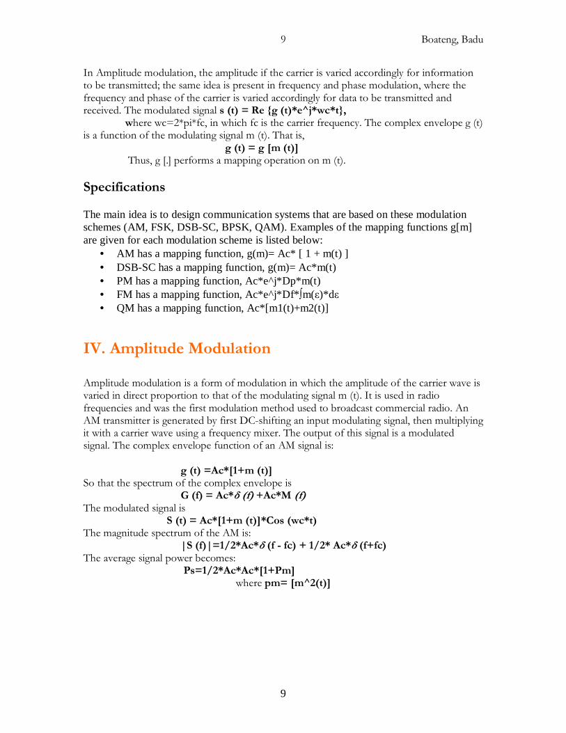
AM transmitter The AM transmitter was generated using the Simulink model shown in figure 1-2
Figure 1-2: AM Transmitter in Simulink
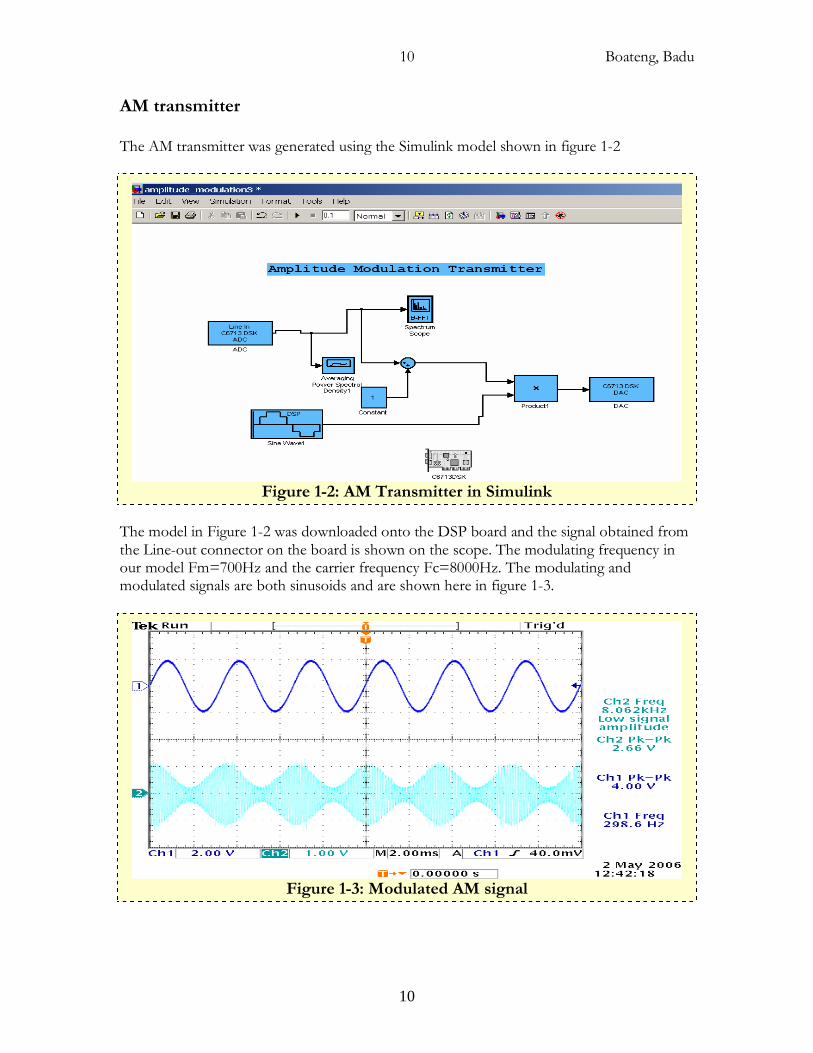
The model in Figure 1-2 was downloaded onto the DSP board and the signal obtained from the Line-out connector on the board is shown on the scope. The modulating frequency in our model Fm=700Hz and the carrier frequency Fc=8000Hz. The modulating and modulated signals are both sinusoids and are shown here in figure 1-3.
Figure 1-3: Modulated AM signal
Boateng, Badu
11
11
The signal on channel 2 is the modulated signal. It shows the input signal forming an envelope around the high frequency carrier signal. Both signals were sampled at a sampling frequency of fss=44100Hz, allowing a bandwidth of 22050Hz for our analysis.
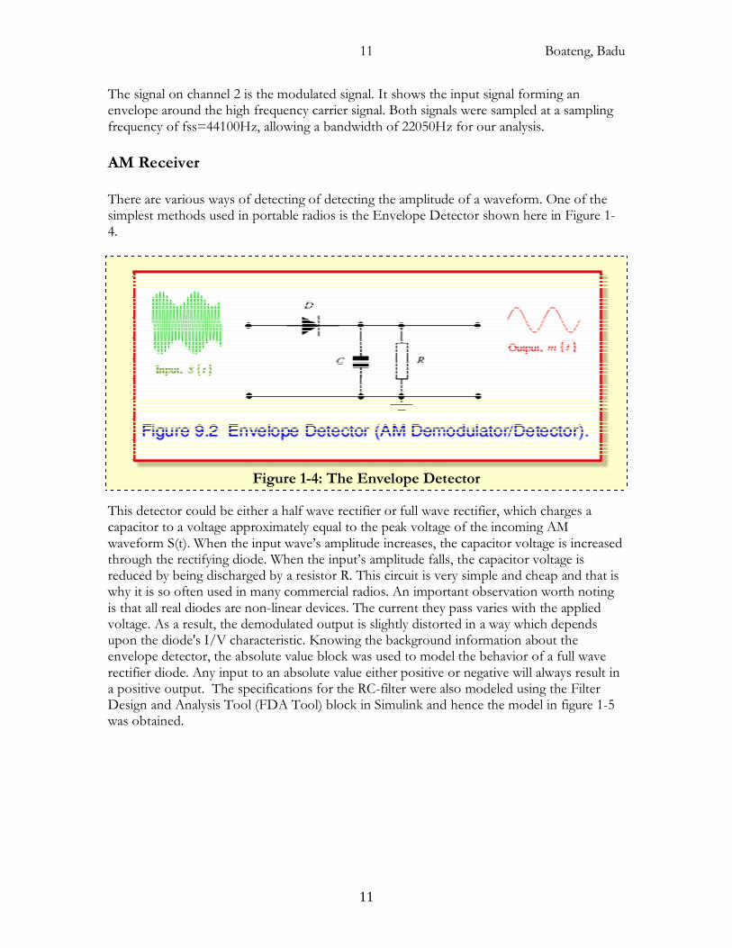
AM Receiver There are various ways of detecting of detecting the amplitude of a waveform. One of the simplest methods used in portable radios is the Envelope Detector shown here in Figure 1-4.
Figure 1-4: The Envelope Detector
This detector could be either a half wave rectifier or full wave rectifier, which charges a capacitor to a voltage approximately equal to the peak voltage of the incoming AM waveform S(t). When the input wave’s amplitude increases, the capacitor voltage is increased through the rectifying diode. When the input’s amplitude falls, the capacitor voltage is reduced by being discharged by a resistor R. This circuit is very simple and cheap and that is why it is so often used in many commercial radios. An important observation worth noting is that all real diodes are non-linear devices. The current they pass varies with the applied voltage. As a result, the demodulated output is slightly distorted in a way which depends upon the diode's I/V characteristic. Knowing the background information about the envelope detector, the absolute value block was used to model the behavior of a full wave rectifier diode. Any input to an absolute value either positive or negative will always result in a positive output. The specifications for the RC-filter were also modeled using the Filter Design and Analysis Tool (FDA Tool) block in Simulink and hence the model in figure 1-5 was obtained.
Boateng, Badu
12
12
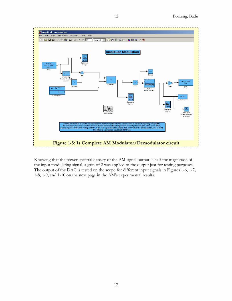
Figure 1-5: Is Complete AM Modulator/Demodulator circuit
Knowing that the power spectral density of the AM signal output is half the magnitude of the input modulating signal, a gain of 2 was applied to the output just for testing purposes. The output of the DAC is tested on the scope for different input signals in Figures 1-6, 1-7, 1-8, 1-9, and 1-10 on the next page in the AM’s experimental results.
Boateng, Badu
13
13
AM Experimental Results
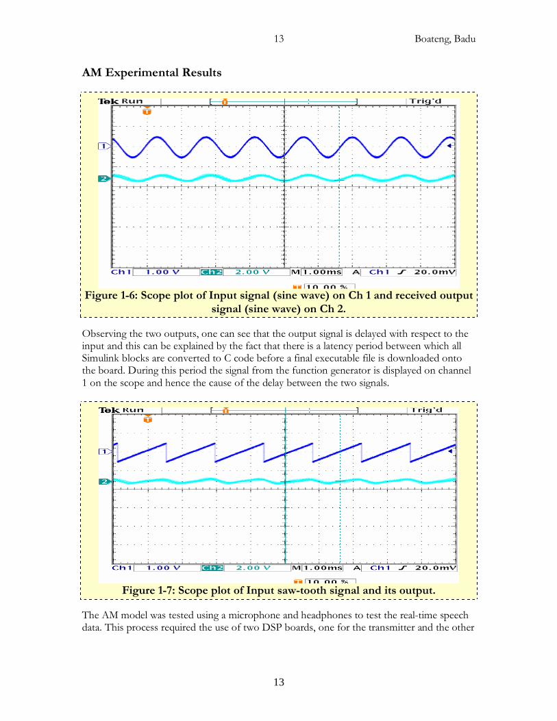
Figure 1-6: Scope plot of Input signal (sine wave) on Ch 1 and received output
signal (sine wave) on Ch 2.
Observing the two outputs, one can see that the output signal is delayed with respect to the input and this can be explained by the fact that there is a latency period between which all Simulink blocks are converted to C code before a final executable file is downloaded onto the board. During this period the signal from the function generator is displayed on channel 1 on the scope and hence the cause of the delay between the two signals.
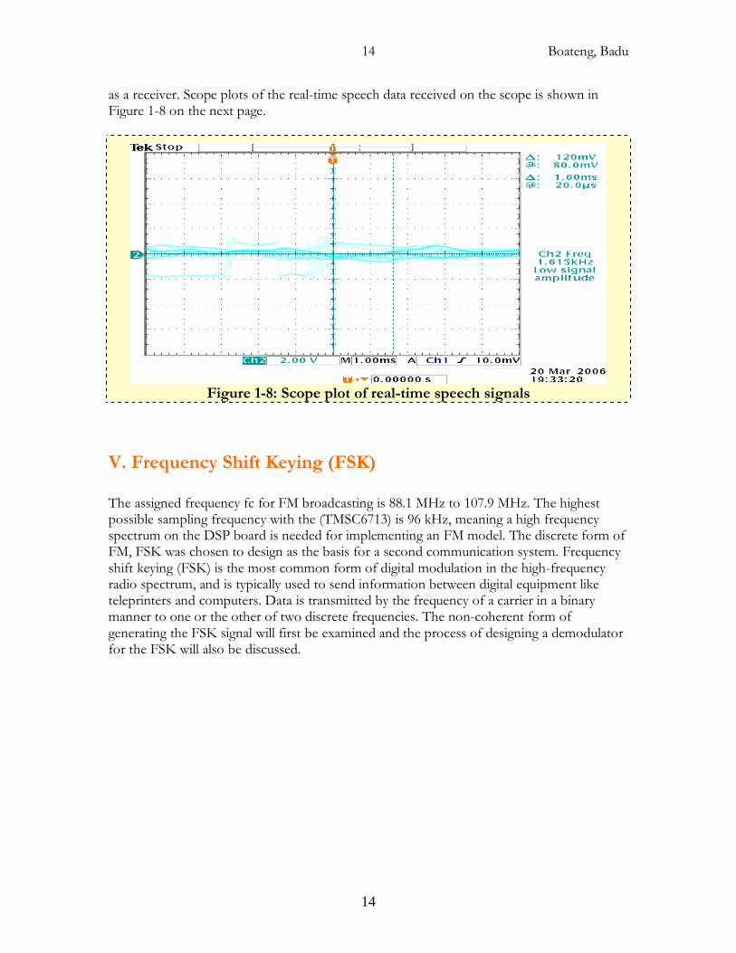
Figure 1-7: Scope plot of Input saw-tooth signal and its output.
The AM model was tested using a microphone and headphones to test the real-time speech data. This process required the use of two DSP boards, one for the transmitter and the other
Boateng, Badu
14
14
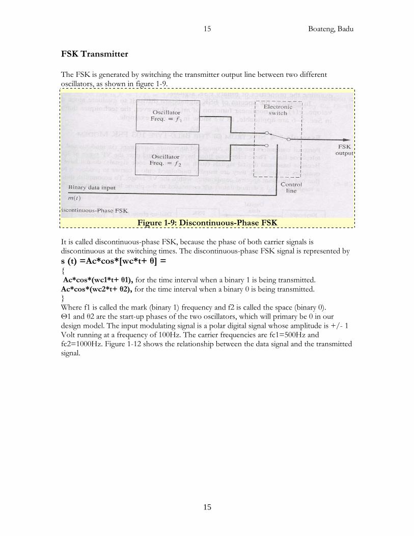
as a receiver. Scope plots of the real-time speech data received on the scope is shown in Figure 1-8 on the next page.
Figure 1-8: Scope plot of real-time speech signals
V. Frequency Shift Keying (FSK) The assigned frequency fc for FM broadcasting is 88.1 MHz to 107.9 MHz. The highest possible sampling frequency with the (TMSC6713) is 96 kHz, meaning a high frequency spectrum on the DSP board is needed for implementing an FM model. The discrete form of FM, FSK was chosen to design as the basis for a second communication system. Frequency shift keying (FSK) is the most common form of digital modulation in the high-frequency radio spectrum, and is typically used to send information between digital equipment like teleprinters and computers. Data is transmitted by the frequency of a carrier in a binary manner to one or the other of two discrete frequencies. The non-coherent form of generating the FSK signal will first be examined and the process of designing a demodulator for the FSK will also be discussed.
Boateng, Badu
15
15
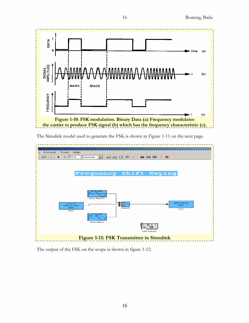
FSK Transmitter The FSK is generated by switching the transmitter output line between two different oscillators, as shown in figure 1-9.
Figure 1-9: Discontinuous-Phase FSK
It is called discontinuous-phase FSK, because the phase of both carrier signals is discontinuous at the switching times. The discontinuous-phase FSK signal is represented by
s (t) =Ac*cos*[wc*t+ θ] = { Ac*cos*(wc1*t+ θ1), for the time interval when a binary 1 is being transmitted. Ac*cos*(wc2*t+ θ2), for the time interval when a binary 0 is being transmitted. } Where f1 is called the mark (binary 1) frequency and f2 is called the space (binary 0). Θ1 and θ2 are the start-up phases of the two oscillators, which will primary be 0 in our design model. The input modulating signal is a polar digital signal whose amplitude is +/- 1 Volt running at a frequency of 100Hz. The carrier frequencies are fc1=500Hz and fc2=1000Hz. Figure 1-12 shows the relationship between the data signal and the transmitted signal.
Boateng, Badu
16
16
Figure 1-10: FSK modulation. Binary Data (a) Frequency modulates
the carrier to produce FSK signal (b) which has the frequency characteristic (c). The Simulink model used to generate the FSK is shown in Figure 1-11 on the next page.
Figure 1-11: FSK Transmitter in Simulink
The output of the FSK on the scope is shown in figure 1-12.
Boateng, Badu
17
17
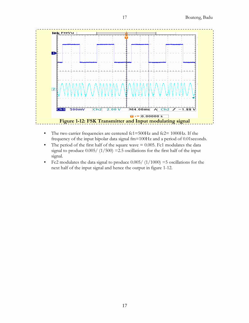
Figure 1-12: FSK Transmitter and Input modulating signal
• The two carrier frequencies are centered fc1=500Hz and fc2= 1000Hz. If the frequency of the input bipolar data signal fm=100Hz and a period of 0.01seconds.
• The period of the first half of the square wave = 0.005. Fc1 modulates the data signal to produce 0.005/ (1/500) =2.5 oscillations for the first half of the input signal.
• Fc2 modulates the data signal to produce 0.005/ (1/1000) =5 oscillations for the next half of the input signal and hence the output in figure 1-12.
Boateng, Badu
18
18
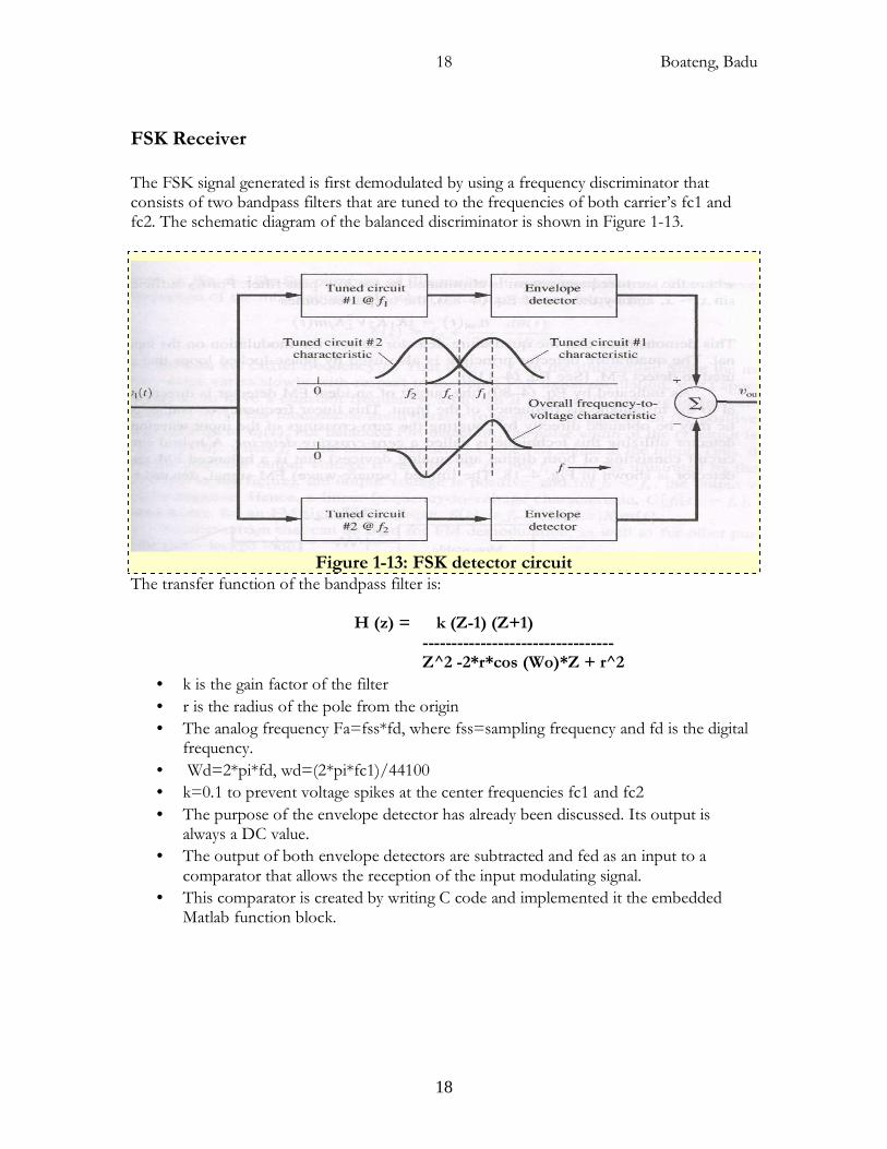
FSK Receiver The FSK signal generated is first demodulated by using a frequency discriminator that consists of two bandpass filters that are tuned to the frequencies of both carrier’s fc1 and fc2. The schematic diagram of the balanced discriminator is shown in Figure 1-13.
Figure 1-13: FSK detector circuit
The transfer function of the bandpass filter is:
H (z) = k (Z-1) (Z+1) --------------------------------- Z^2 -2*r*cos (Wo)*Z + r^2
• k is the gain factor of the filter
• r is the radius of the pole from the origin
• The analog frequency Fa=fss*fd, where fss=sampling frequency and fd is the digital frequency.
• Wd=2*pi*fd, wd=(2*pi*fc1)/44100
• k=0.1 to prevent voltage spikes at the center frequencies fc1 and fc2
• The purpose of the envelope detector has already been discussed. Its output is always a DC value.
• The output of both envelope detectors are subtracted and fed as an input to a comparator that allows the reception of the input modulating signal.
• This comparator is created by writing C code and implemented it the embedded Matlab function block.
Boateng, Badu
19
19
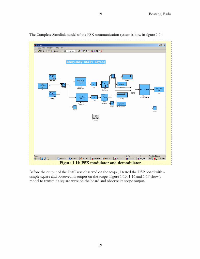
The Complete Simulink model of the FSK communication system is how in figure 1-14.
Figure 1-14: FSK modulator and demodulator
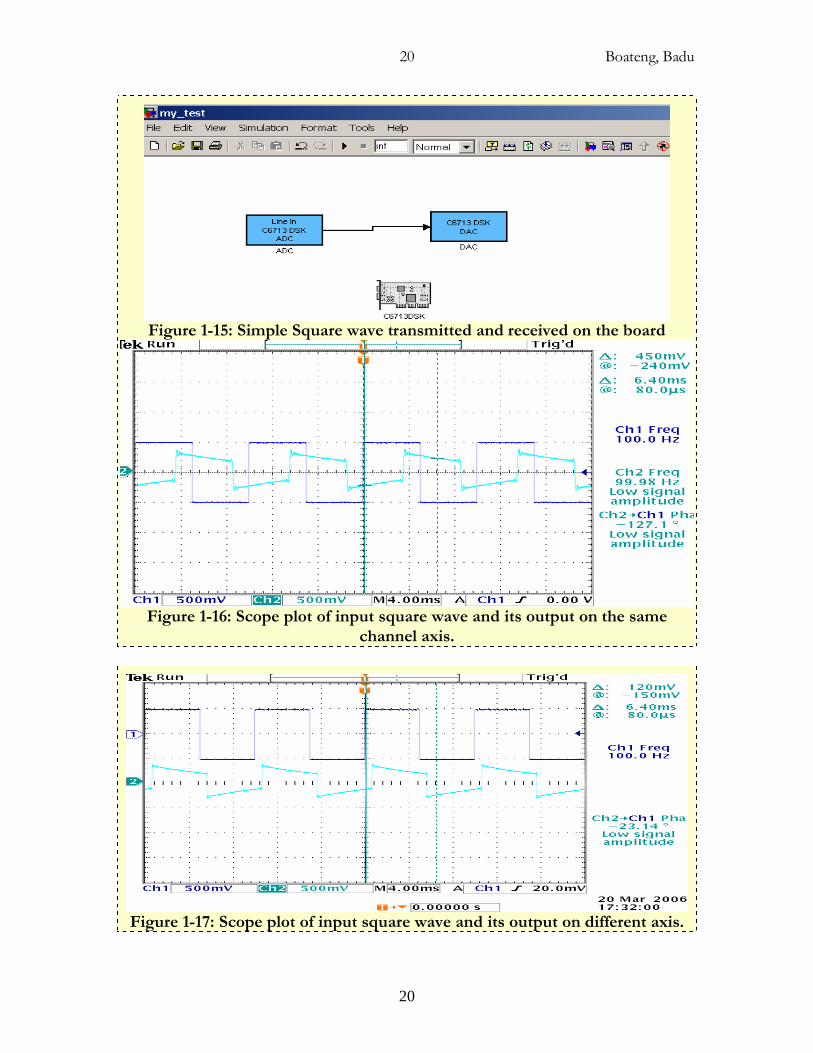
Before the output of the DAC was observed on the scope, I tested the DSP board with a simple square and observed its output on the scope. Figure 1-15, 1-16 and 1-17 show a model to transmit a square wave on the board and observe its scope output.
Boateng, Badu
20
20
Figure 1-15: Simple Square wave transmitted and received on the board
Figure 1-16: Scope plot of input square wave and its output on the same
channel axis.
Figure 1-17: Scope plot of input square wave and its output on different axis.
Boateng, Badu
21
21
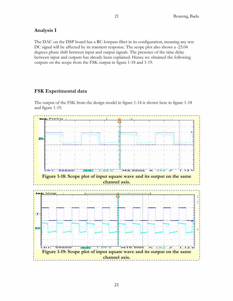
Analysis I The DAC on the DSP board has a RC-lowpass filter in its configuration, meaning any test DC signal will be affected by its transient response. The scope plot also shows a -23.04 degrees phase shift between input and output signals. The presence of the time delay between input and outputs has already been explained. Hence we obtained the following outputs on the scope from the FSK output in figure 1-18 and 1-19.
FSK Experimental data The output of the FSK from the design model in figure 1-14 is shown here in figure 1-18 and figure 1-19.
Figure 1-18: Scope plot of input square wave and its output on the same
channel axis.
Figure 1-19: Scope plot of input square wave and its output on the same
channel axis.
Boateng, Badu
22
22
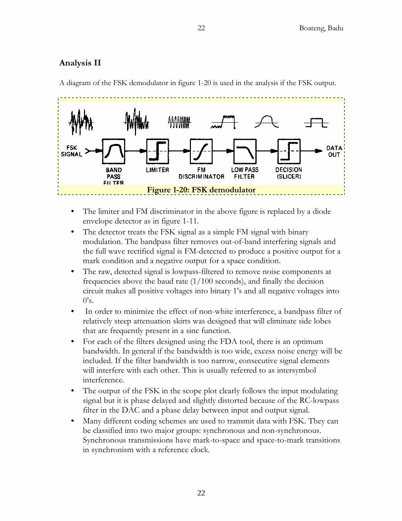
Analysis II A diagram of the FSK demodulator in figure 1-20 is used in the analysis if the FSK output.
Figure 1-20: FSK demodulator
• The limiter and FM discriminator in the above figure is replaced by a diode envelope detector as in figure 1-11.
• The detector treats the FSK signal as a simple FM signal with binary modulation. The bandpass filter removes out-of-band interfering signals and the full wave rectified signal is FM-detected to produce a positive output for a mark condition and a negative output for a space condition.
• The raw, detected signal is lowpass-filtered to remove noise components at frequencies above the baud rate (1/100 seconds), and finally the decision circuit makes all positive voltages into binary 1’s and all negative voltages into 0’s.
• In order to minimize the effect of non-white interference, a bandpass filter of relatively steep attenuation skirts was designed that will eliminate side lobes that are frequently present in a sinc function.
• For each of the filters designed using the FDA tool, there is an optimum bandwidth. In general if the bandwidth is too wide, excess noise energy will be included. If the filter bandwidth is too narrow, consecutive signal elements will interfere with each other. This is usually referred to as intersymbol interference.
• The output of the FSK in the scope plot clearly follows the input modulating signal but it is phase delayed and slightly distorted because of the RC-lowpass filter in the DAC and a phase delay between input and output signal.
• Many different coding schemes are used to transmit data with FSK. They can be classified into two major groups: synchronous and non-synchronous. Synchronous transmissions have mark-to-space and space-to-mark transitions in synchronism with a reference clock.
Boateng, Badu
23
23
• A common synchronous system uses Moore ARQ coding. The Moore code is a 7-bitper-character code with no start or stop elements. Bit synchronization is maintained by using a reference clock which tracks the keying speed of the received signal. Character synchronization is maintained by sending periodic “idle” or “dummy” characters between valid data characters.
VI. Double-Sideband Suppressed Carrier (DSB-SC) A double-sideband suppressed carrier signal is an AM signal that has a suppressed discrete carrier. The DSB-SC signal is given by:
S (t) = Ac*m (t)*cos (wc*t) Where m (t) is assumed to have a zero dc level for the suppressed carrier case. The spectrum is identical to that for the AM, except that the delta functions at (+/- fc) are missing. That is the spectrum for the DSB-SC is S (f) = 0.5*Ac*[M (f-fc) + M (f+fc)] Compared with an AM signal, the percentage of the modulation on the DSB-SC signal is infinite, because there is no carrier line component. Also, the modulation efficiency of the DSB-SC signal is 100%, since no power is wasted in a discrete carrier. However a product detector is used for demodulation. If m (t) is a polar binary data signal instead of an audio signal, the s (t) will be a Binary Polar shift Keying (BPSK).
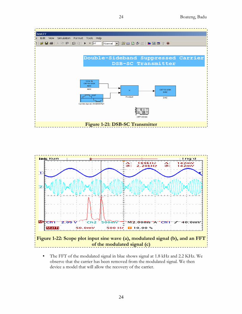
DSB-SC Transmitter The transmitter for the DSB-SC is generated by multiplying an input sine wave at modulating frequency fm=200 Hz to a carrier sine wave whose frequency is fc=2000 Hz. Figure 1-21 is a Simulink model of the DSB-SC transmitter. Its output on the scope is shown in figure 1-22 on the next page.
Boateng, Badu
24
24
Figure 1-21: DSB-SC Transmitter
Figure 1-22: Scope plot input sine wave (a), modulated signal (b), and an FFT of the modulated signal (c)
• The FFT of the modulated signal in blue shows signal at 1.8 kHz and 2.2 KHz. We observe that the carrier has been removed from the modulated signal. We then device a model that will allow the recovery of the carrier.
Boateng, Badu
25
25
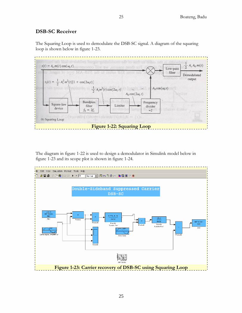
DSB-SC Receiver The Squaring Loop is used to demodulate the DSB-SC signal. A diagram of the squaring loop is shown below in figure 1-23.
Figure 1-22: Squaring Loop
The diagram in figure 1-22 is used to design a demodulator in Simulink model below in figure 1-23 and its scope plot is shown in figure 1-24.
Figure 1-23: Carrier recovery of DSB-SC using Squaring Loop
Boateng, Badu
26
26
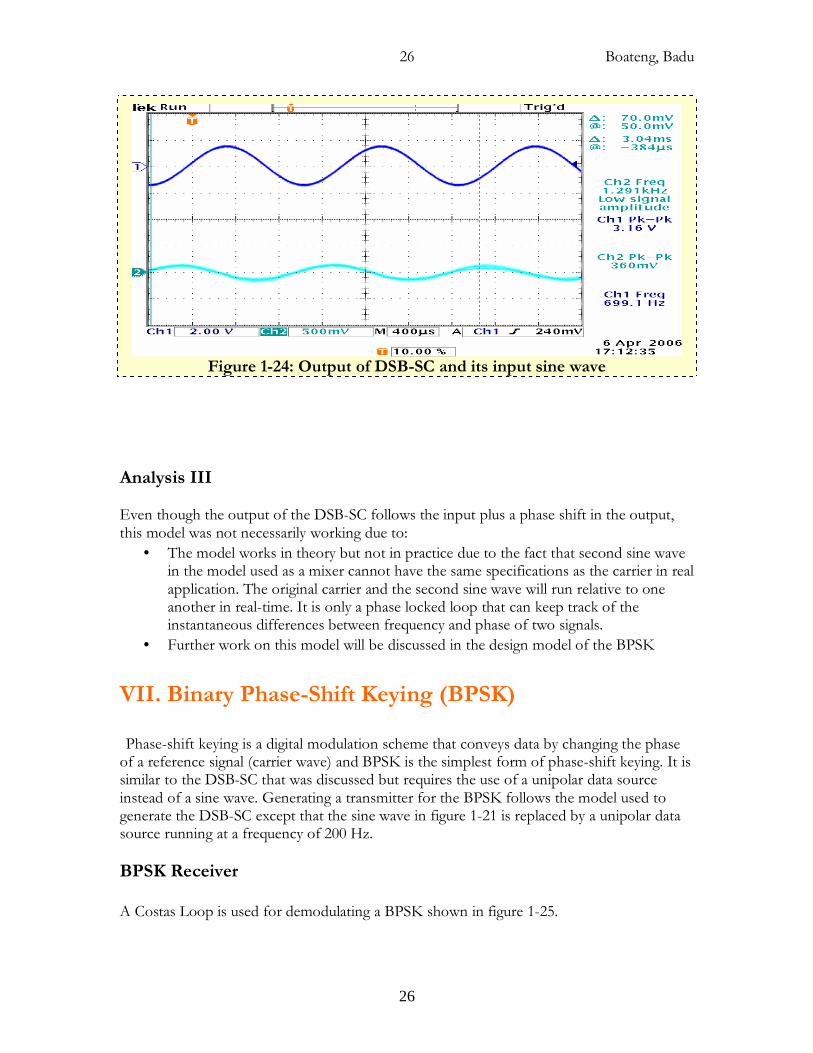
Figure 1-24: Output of DSB-SC and its input sine wave
Analysis III Even though the output of the DSB-SC follows the input plus a phase shift in the output, this model was not necessarily working due to:
• The model works in theory but not in practice due to the fact that second sine wave in the model used as a mixer cannot have the same specifications as the carrier in real application. The original carrier and the second sine wave will run relative to one another in real-time. It is only a phase locked loop that can keep track of the instantaneous differences between frequency and phase of two signals.
• Further work on this model will be discussed in the design model of the BPSK
VII. Binary Phase-Shift Keying (BPSK) Phase-shift keying is a digital modulation scheme that conveys data by changing the phase of a reference signal (carrier wave) and BPSK is the simplest form of phase-shift keying. It is similar to the DSB-SC that was discussed but requires the use of a unipolar data source instead of a sine wave. Generating a transmitter for the BPSK follows the model used to generate the DSB-SC except that the sine wave in figure 1-21 is replaced by a unipolar data source running at a frequency of 200 Hz.
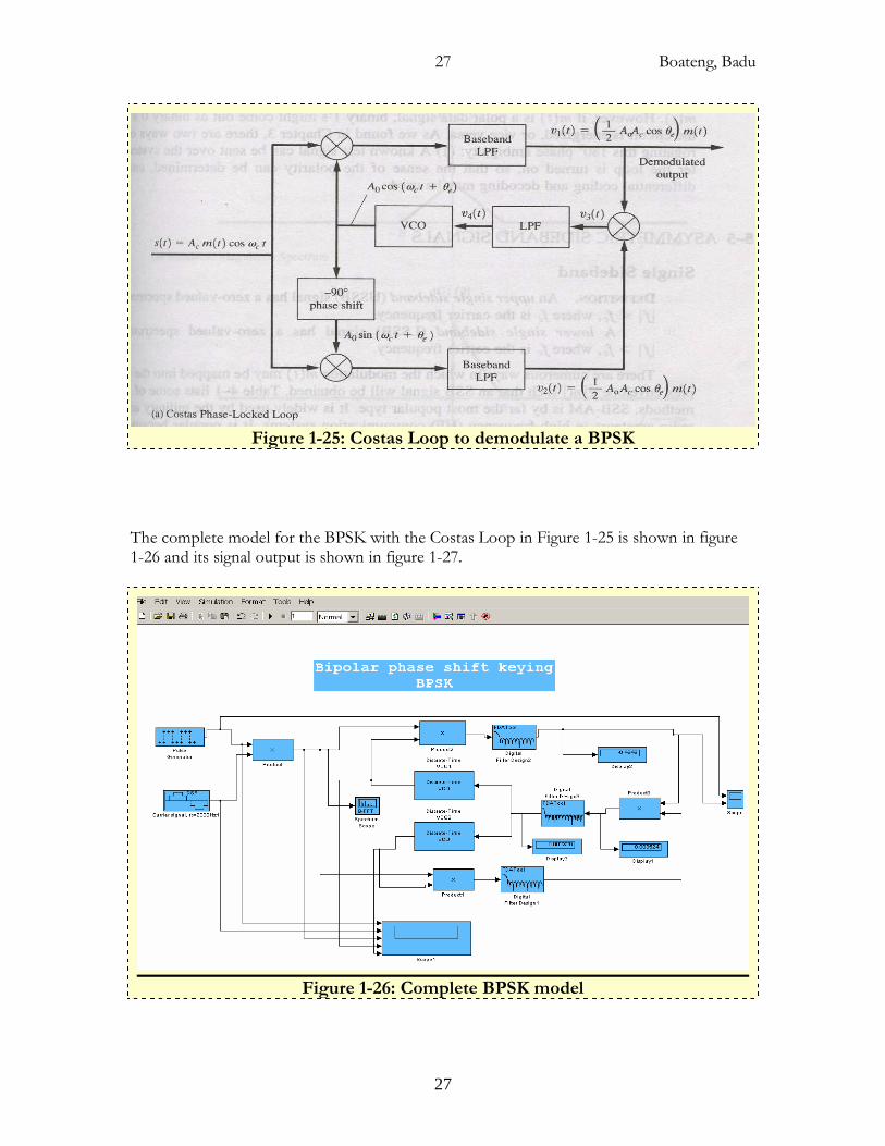
BPSK Receiver A Costas Loop is used for demodulating a BPSK shown in figure 1-25.
Boateng, Badu
27
27
Figure 1-25: Costas Loop to demodulate a BPSK
The complete model for the BPSK with the Costas Loop in Figure 1-25 is shown in figure 1-26 and its signal output is shown in figure 1-27.
Figure 1-26: Complete BPSK model
Boateng, Badu
28
28
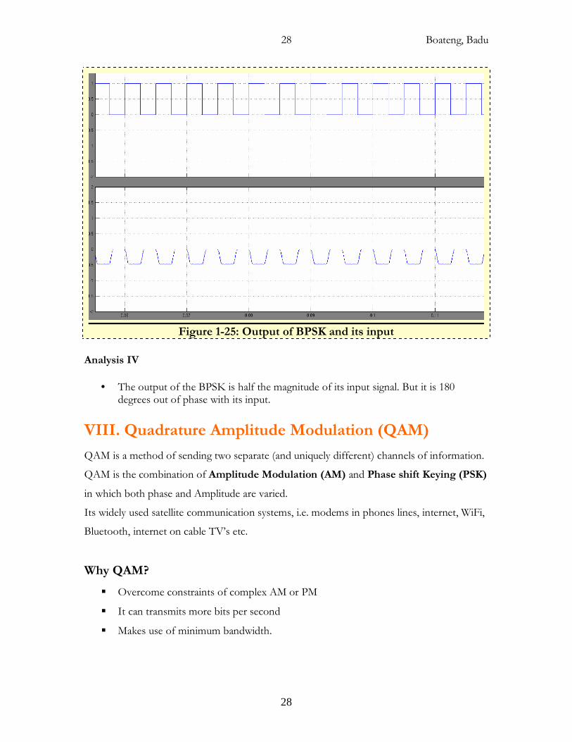
Figure 1-25: Output of BPSK and its input
Analysis IV
• The output of the BPSK is half the magnitude of its input signal. But it is 180 degrees out of phase with its input.
VIII. Quadrature Amplitude Modulation (QAM)
QAM is a method of sending two separate (and uniquely different) channels of information.
QAM is the combination of Amplitude Modulation (AM) and Phase shift Keying (PSK)
in which both phase and Amplitude are varied.
Its widely used satellite communication systems, i.e. modems in phones lines, internet, WiFi,
Bluetooth, internet on cable TV’s etc.
Why QAM?
� Overcome constraints of complex AM or PM
� It can transmits more bits per second
� Makes use of minimum bandwidth.
Boateng, Badu
29
29
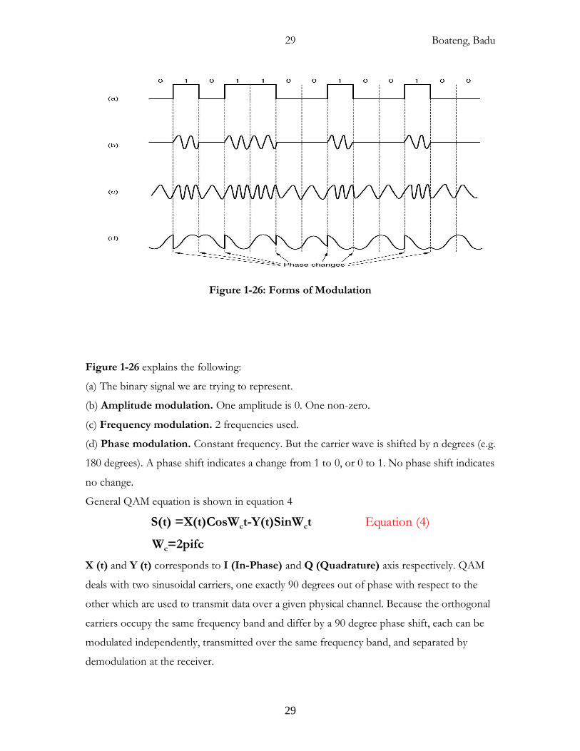
Figure 1-26: Forms of Modulation
Figure 1-26 explains the following:
(a) The binary signal we are trying to represent.
(b) Amplitude modulation. One amplitude is 0. One non-zero.
(c) Frequency modulation. 2 frequencies used.
(d) Phase modulation. Constant frequency. But the carrier wave is shifted by n degrees (e.g.
180 degrees). A phase shift indicates a change from 1 to 0, or 0 to 1. No phase shift indicates
no change.
General QAM equation is shown in equation 4
S(t) =X(t)CosWct-Y(t)SinWct Equation (4)
Wc=2pifc
X (t) and Y (t) corresponds to I (In-Phase) and Q (Quadrature) axis respectively. QAM
deals with two sinusoidal carriers, one exactly 90 degrees out of phase with respect to the
other which are used to transmit data over a given physical channel. Because the orthogonal
carriers occupy the same frequency band and differ by a 90 degree phase shift, each can be
modulated independently, transmitted over the same frequency band, and separated by
demodulation at the receiver.
Boateng, Badu
30
30
QAM MODULATOR
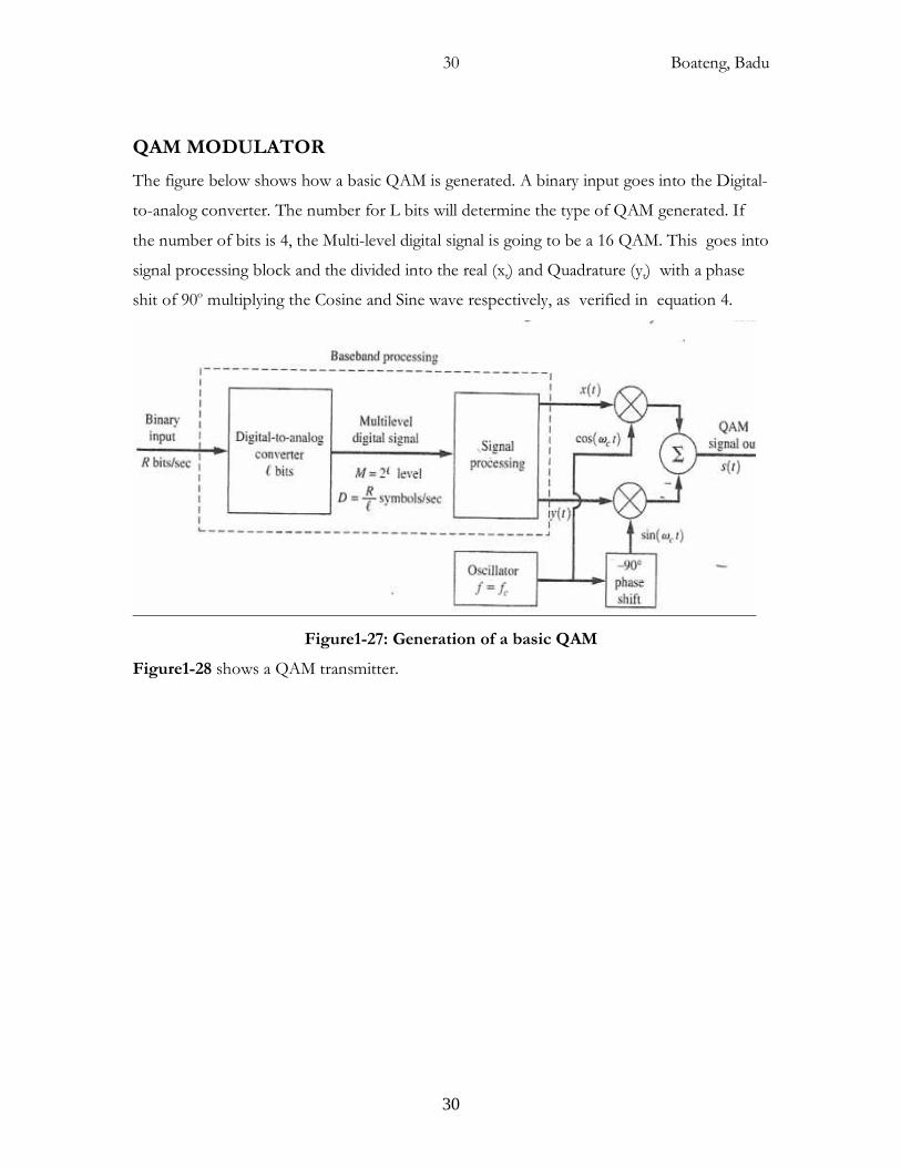
The figure below shows how a basic QAM is generated. A binary input goes into the Digital-
to-analog converter. The number for L bits will determine the type of QAM generated. If
the number of bits is 4, the Multi-level digital signal is going to be a 16 QAM. This goes into
signal processing block and the divided into the real (xt) and Quadrature (yt) with a phase
shit of 90o multiplying the Cosine and Sine wave respectively, as verified in equation 4.
Figure1-27: Generation of a basic QAM
Figure1-28 shows a QAM transmitter.
Boateng, Badu
31
31
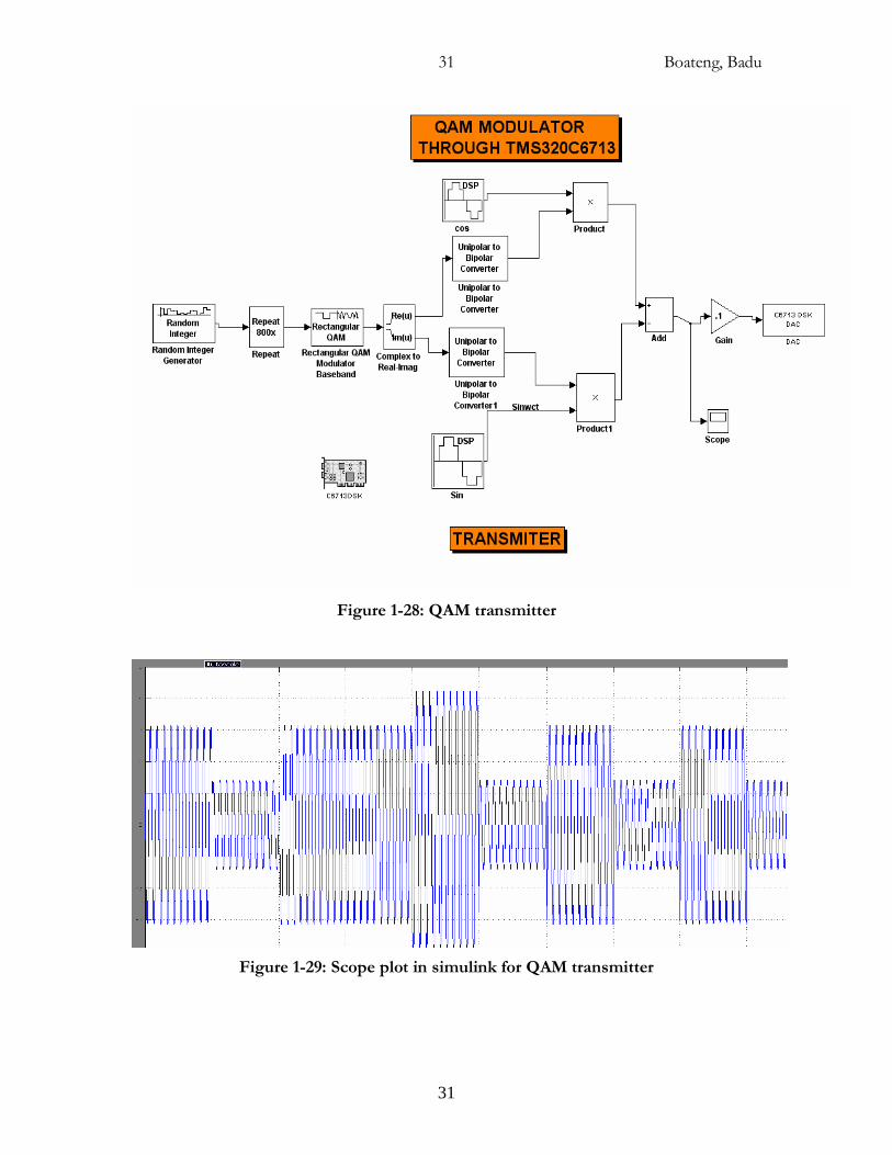
Figure 1-28: QAM transmitter
Figure 1-29: Scope plot in simulink for QAM transmitter
Boateng, Badu
32
32
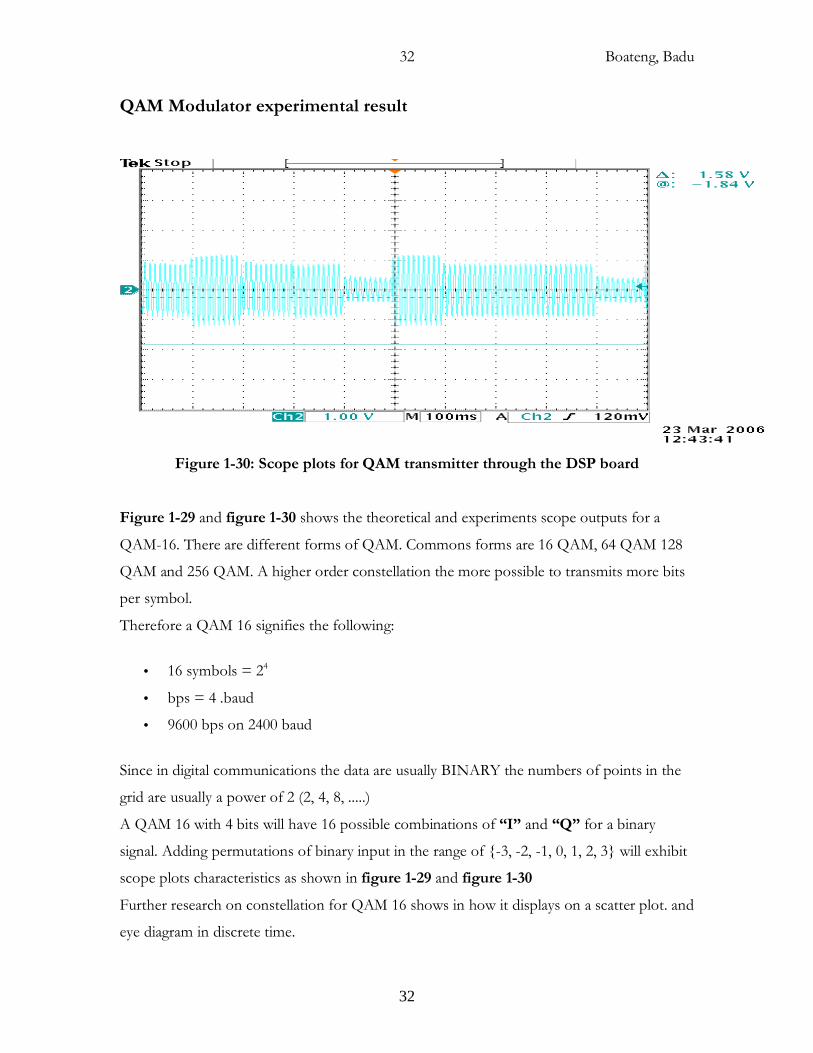
QAM Modulator experimental result
Figure 1-30: Scope plots for QAM transmitter through the DSP board
Figure 1-29 and figure 1-30 shows the theoretical and experiments scope outputs for a
QAM-16. There are different forms of QAM. Commons forms are 16 QAM, 64 QAM 128
QAM and 256 QAM. A higher order constellation the more possible to transmits more bits
per symbol.
Therefore a QAM 16 signifies the following:
• 16 symbols = 24
• bps = 4 .baud
• 9600 bps on 2400 baud
Since in digital communications the data are usually BINARY the numbers of points in the
grid are usually a power of 2 (2, 4, 8, .....)
A QAM 16 with 4 bits will have 16 possible combinations of “I” and “Q” for a binary
signal. Adding permutations of binary input in the range of {-3, -2, -1, 0, 1, 2, 3} will exhibit
scope plots characteristics as shown in figure 1-29 and figure 1-30
Further research on constellation for QAM 16 shows in how it displays on a scatter plot. and
eye diagram in discrete time.
Boateng, Badu
33
33
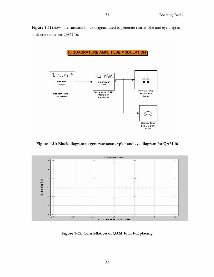
Figure 1-31 shows the simulink block diagram used to generate scatter plot and eye diagram
in discrete time for QAM 16.
Figure 1-31: Block diagram to generate scatter plot and eye diagram for QAM 16
Figure 1-32: Constellation of QAM 16 in full placing
Boateng, Badu
34
34
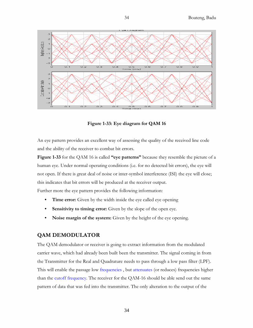
Figure 1-33: Eye diagram for QAM 16
An eye pattern provides an excellent way of assessing the quality of the received line code
and the ability of the receiver to combat bit errors.
Figure 1-33 for the QAM 16 is called “eye patterns” because they resemble the picture of a
human eye. Under normal operating conditions (i.e. for no detected bit errors), the eye will
not open. If there is great deal of noise or inter-symbol interference (ISI) the eye will close;
this indicates that bit errors will be produced at the receiver output.
Further more the eye pattern provides the following information:
• Time error: Given by the width inside the eye called eye opening
• Sensitivity to timing error: Given by the slope of the open eye.
• Noise margin of the system: Given by the height of the eye opening.
QAM DEMODULATOR
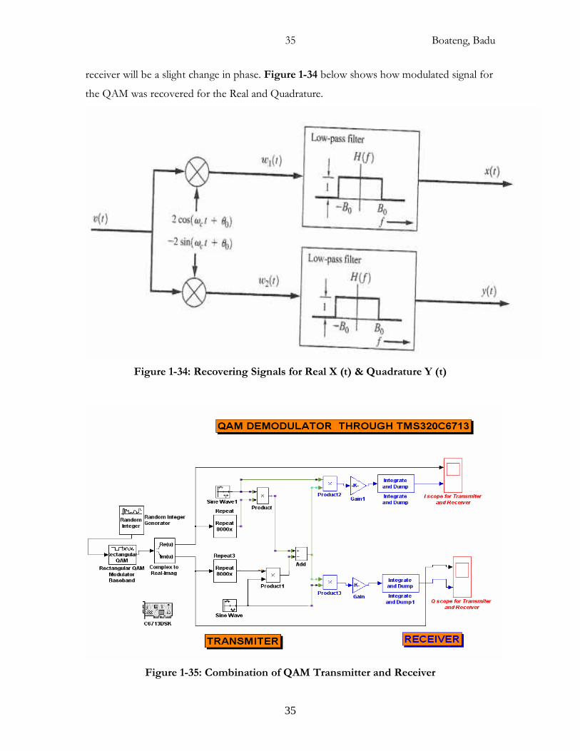
The QAM demodulator or receiver is going to extract information from the modulated
carrier wave, which had already been built been the transmitter. The signal coming in from
the Transmitter for the Real and Quadrature needs to pass through a low pass filter (LPF).
This will enable the passage low frequencies , but attenuates (or reduces) frequencies higher
than the cutoff frequency. The receiver for the QAM-16 should be able send out the same
pattern of data that was fed into the transmitter. The only alteration to the output of the
Boateng, Badu
35
35
receiver will be a slight change in phase. Figure 1-34 below shows how modulated signal for
the QAM was recovered for the Real and Quadrature.
Figure 1-34: Recovering Signals for Real X (t) & Quadrature Y (t)
Figure 1-35: Combination of QAM Transmitter and Receiver
Boateng, Badu
36
36
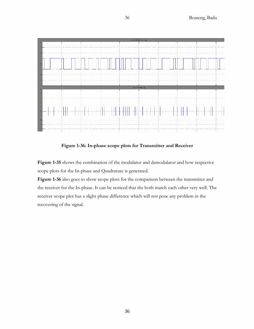
Figure 1-36: In-phase scope plots for Transmitter and Receiver
Figure 1-35 shows the combination of the modulator and demodulator and how respective
scope plots for the In-phase and Quadrature is generated.
Figure 1-36 also goes to show scope plots for the comparison between the transmitter and
the receiver for the In-phase. It can be noticed that the both match each other very well. The
receiver scope plot has a slight phase difference which will not pose any problem in the
recovering of the signal.
Boateng, Badu
37
37
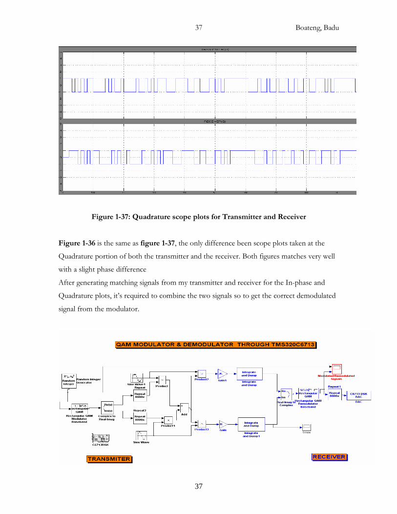
Figure 1-37: Quadrature scope plots for Transmitter and Receiver
Figure 1-36 is the same as figure 1-37, the only difference been scope plots taken at the
Quadrature portion of both the transmitter and the receiver. Both figures matches very well
with a slight phase difference
After generating matching signals from my transmitter and receiver for the In-phase and
Quadrature plots, it’s required to combine the two signals so to get the correct demodulated
signal from the modulator.
Boateng, Badu
38
38
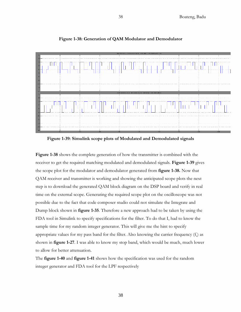
Figure 1-38: Generation of QAM Modulator and Demodulator
Figure 1-39: Simulink scope plots of Modulated and Demodulated signals
Figure 1-38 shows the complete generation of how the transmitter is combined with the
receiver to get the required matching modulated and demodulated signals. Figure 1-39 gives
the scope plot for the modulator and demodulator generated from figure 1-38. Now that
QAM receiver and transmitter is working and showing the anticipated scope plots the next
step is to download the generated QAM block diagram on the DSP board and verify in real
time on the external scope. Generating the required scope plot on the oscilloscope was not
possible due to the fact that code composer studio could not simulate the Integrate and
Dump block shown in figure 1-35. Therefore a new approach had to be taken by using the
FDA tool in Simulink to specify specifications for the filter. To do that I, had to know the
sample time for my random integer generator. This will give me the hint to specify
appropriate values for my pass band for the filter. Also knowing the carrier frequency (fc) as
shown in figure 1-27. I was able to know my stop band, which would be much, much lower
to allow for better attenuation.
The figure 1-40 and figure 1-41 shows how the specification was used for the random
integer generator and FDA tool for the LPF respectively
Boateng, Badu
39
39
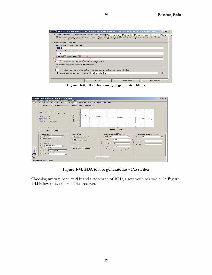
Figure 1-40: Random integer generator block
Figure 1-41: FDA tool to generate Low Pass Filter
Choosing my pass band to 2Hz and a stop band of 10Hz, a receiver block was built. Figure 1-42 below shows the modified receiver.
Boateng, Badu
40
40
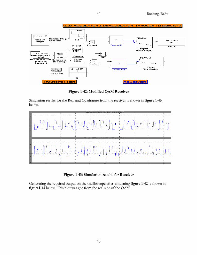
Figure 1-42: Modified QAM Receiver
Simulation results for the Real and Quadrature from the receiver is shown in figure 1-43 below.
Figure 1-43: Simulation results for Receiver
Generating the required output on the oscilloscope after simulating figure 1-42 is shown in figure1-43 below. This plot was got from the real side of the QAM.
Boateng, Badu
41
41
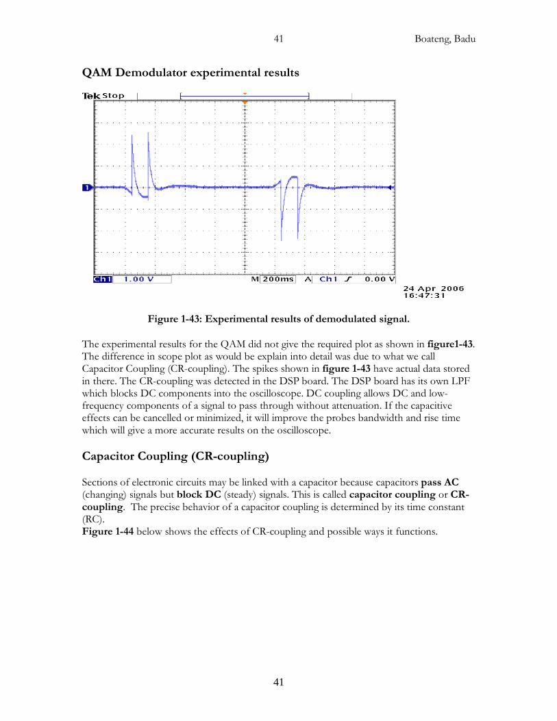
QAM Demodulator experimental results
Figure 1-43: Experimental results of demodulated signal.
The experimental results for the QAM did not give the required plot as shown in figure1-43. The difference in scope plot as would be explain into detail was due to what we call Capacitor Coupling (CR-coupling). The spikes shown in figure 1-43 have actual data stored in there. The CR-coupling was detected in the DSP board. The DSP board has its own LPF which blocks DC components into the oscilloscope. DC coupling allows DC and low-frequency components of a signal to pass through without attenuation. If the capacitive effects can be cancelled or minimized, it will improve the probes bandwidth and rise time which will give a more accurate results on the oscilloscope.
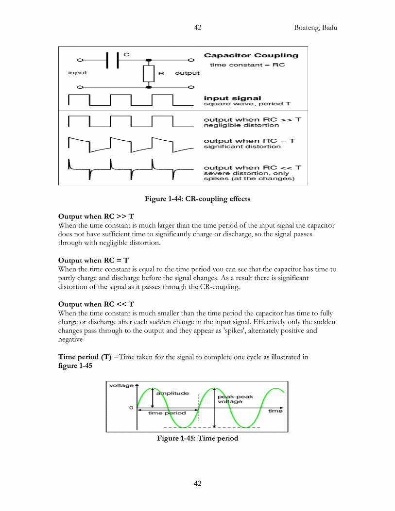
Capacitor Coupling (CR-coupling)
Sections of electronic circuits may be linked with a capacitor because capacitors pass AC (changing) signals but block DC (steady) signals. This is called capacitor coupling or CR-coupling. The precise behavior of a capacitor coupling is determined by its time constant (RC). Figure 1-44 below shows the effects of CR-coupling and possible ways it functions.
Boateng, Badu
42
42
Figure 1-44: CR-coupling effects
Output when RC >> T When the time constant is much larger than the time period of the input signal the capacitor does not have sufficient time to significantly charge or discharge, so the signal passes through with negligible distortion.
Output when RC = T When the time constant is equal to the time period you can see that the capacitor has time to partly charge and discharge before the signal changes. As a result there is significant distortion of the signal as it passes through the CR-coupling.
Output when RC << T When the time constant is much smaller than the time period the capacitor has time to fully charge or discharge after each sudden change in the input signal. Effectively only the sudden changes pass through to the output and they appear as 'spikes', alternately positive and negative
Time period (T) =Time taken for the signal to complete one cycle as illustrated in figure 1-45
Figure 1-45: Time period
Boateng, Badu
43
43
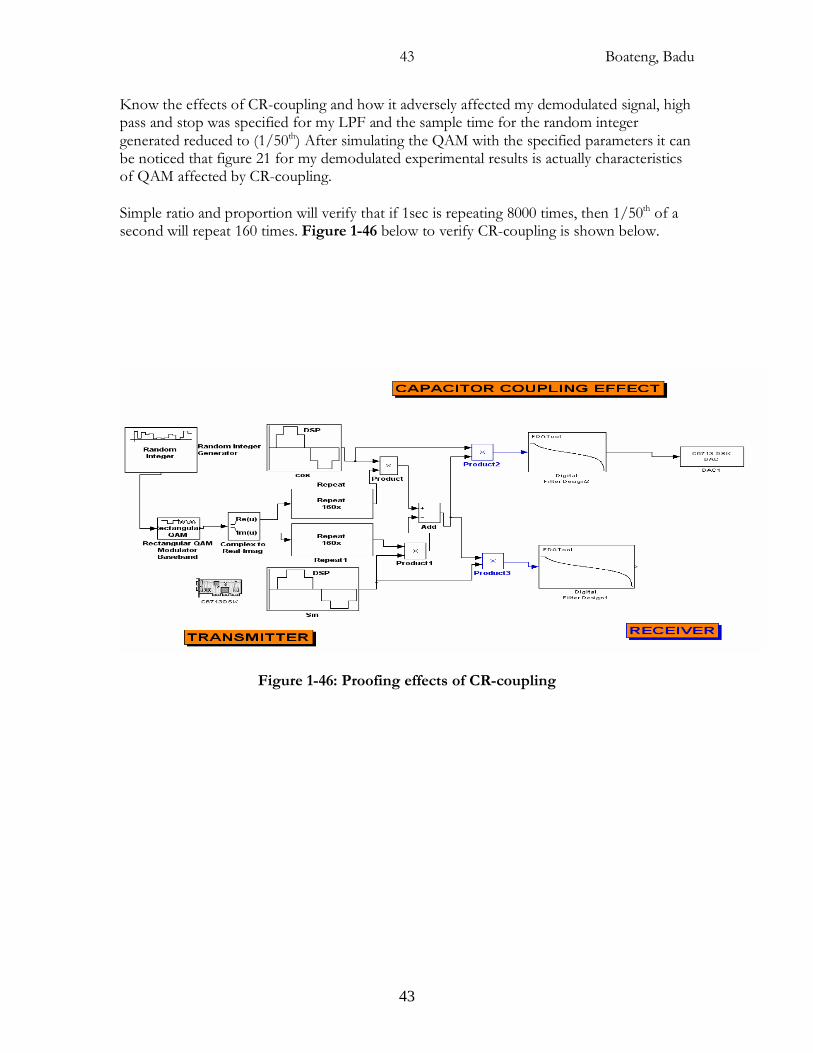
Know the effects of CR-coupling and how it adversely affected my demodulated signal, high pass and stop was specified for my LPF and the sample time for the random integer generated reduced to (1/50th) After simulating the QAM with the specified parameters it can be noticed that figure 21 for my demodulated experimental results is actually characteristics of QAM affected by CR-coupling.
Simple ratio and proportion will verify that if 1sec is repeating 8000 times, then 1/50th of a second will repeat 160 times. Figure 1-46 below to verify CR-coupling is shown below.
Figure 1-46: Proofing effects of CR-coupling
Boateng, Badu
44
44
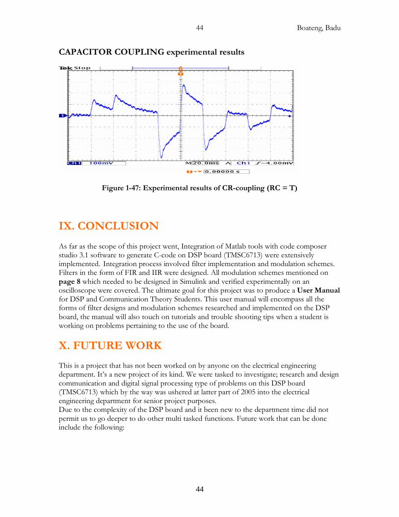
CAPACITOR COUPLING experimental results
Figure 1-47: Experimental results of CR-coupling (RC = T)
IX. CONCLUSION
As far as the scope of this project went, Integration of Matlab tools with code composer studio 3.1 software to generate C-code on DSP board (TMSC6713) were extensively implemented. Integration process involved filter implementation and modulation schemes. Filters in the form of FIR and IIR were designed. All modulation schemes mentioned on page 8 which needed to be designed in Simulink and verified experimentally on an oscilloscope were covered. The ultimate goal for this project was to produce a User Manual for DSP and Communication Theory Students. This user manual will encompass all the forms of filter designs and modulation schemes researched and implemented on the DSP board, the manual will also touch on tutorials and trouble shooting tips when a student is working on problems pertaining to the use of the board.
X. FUTURE WORK This is a project that has not been worked on by anyone on the electrical engineering department. It’s a new project of its kind. We were tasked to investigate; research and design communication and digital signal processing type of problems on this DSP board (TMSC6713) which by the way was ushered at latter part of 2005 into the electrical engineering department for senior project purposes. Due to the complexity of the DSP board and it been new to the department time did not permit us to go deeper to do other multi tasked functions. Future work that can be done include the following:
Boateng, Badu
45
45
• Implement Costas Phase-Locked Loop on DSP board
• Work on Frequency Division Multiplexing (FDM)
• Orthogonal Frequency Division Multiplexing (OFDM)
• FM Stereo System
XI. BIBLIOGRAPHY Text Book:
� Digital and Analog Communication systems 6th Edition (Lean .W. Couch II) Soft ware:
� Matlab Version 7.0
� Code Composer Studio Version 3.1