ee503 topic 2 hoo
TRANSCRIPT
7212019 EE503 Topic 2 Hoo
httpslidepdfcomreaderfullee503-topic-2-hoo 122
89
Topic 2
EE503
IC Fabrication amp Packaging Technology
983120983154983141983152983137983154983141983140 983138983161983098 983109983150983143983154983086 983112983151983151 983117983151983159 983112983141983150983143
7212019 EE503 Topic 2 Hoo
httpslidepdfcomreaderfullee503-topic-2-hoo 222
89
Tens or hundreds of identical chips (die) are fabricated
simultaneously on a silicon wafer (substrate)
Wafer Size (refer ro diagram)
The cost of fabricating ICs drops dramatically ifthere are more chips on a wafer
The number of chips on a wafer variesdepending on the type of product and thelevel of integration on the chip
7212019 EE503 Topic 2 Hoo
httpslidepdfcomreaderfullee503-topic-2-hoo 322
89
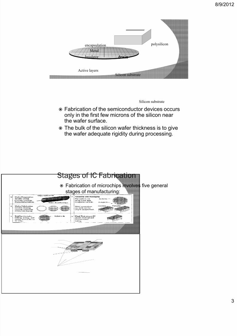
Silicon substrate
draindraindraindrain
Silicon substrate
encapsulation
Metal
Insulator
Active layers
polysilicon
Fabrication of the semiconductor devices occurs
only in the first few microns of the silicon nearthe wafer surface
The bulk of the silicon wafer thickness is to givethe wafer adequate rigidity during processing
Stages of IC Fabrication Fabrication of microchips involves five general
stages of manufacturing
7212019 EE503 Topic 2 Hoo
httpslidepdfcomreaderfullee503-topic-2-hoo 422
89
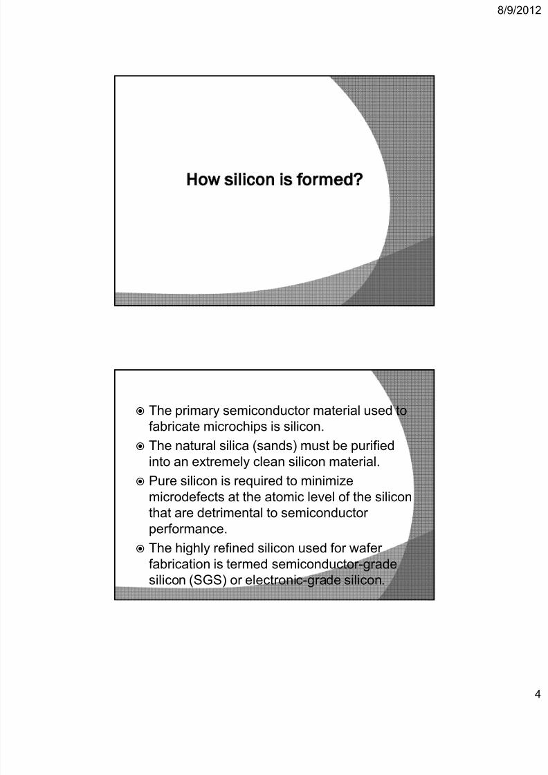
The primary semiconductor material used tofabricate microchips is silicon
The natural silica (sands) must be purified
into an extremely clean silicon material
Pure silicon is required to minimize
microdefects at the atomic level of the silicon
that are detrimental to semiconductor
performance
The highly refined silicon used for waferfabrication is termed semiconductor-grade
silicon (SGS) or electronic-grade silicon
7212019 EE503 Topic 2 Hoo
httpslidepdfcomreaderfullee503-topic-2-hoo 522
89
Steps to Obtaining SemiconductorSteps to Obtaining SemiconductorSteps to Obtaining SemiconductorSteps to Obtaining Semiconductor----Grade Silicon (SGS)Grade Silicon (SGS)Grade Silicon (SGS)Grade Silicon (SGS)
Step Description of Process Purity Rate
1 Produce metallurgical-grade silicon
(MGS) by heating silica with carbon
SiC (s) + SiO2 (s) Si (l) + SiO(g) + CO (g)
98
2 Purify MGS through a chemical reaction to produce
a silicon-bearing gas of trichlorosilane (SiHCl3)
Si (s) + 3HCl (g) SiHCl3 (g) + H2 (g) + heat
-
3 Using the Siemens process SiHCI3 and H2 react
to produce pure semiconductor- grade silicon
(SGS)
2SiHCl3 (g) + 2H2 (g) 2Si (s) + 6HCI (g)
999999999
Semiconductor-grade silicon used to
fabricate semiconductor devices have
ultrahigh purity but it must also have a near-
perfect crystal structure
This condition is necessary to avoid electrical
and mechanical defects that are detrimental
to device performance
7212019 EE503 Topic 2 Hoo
httpslidepdfcomreaderfullee503-topic-2-hoo 622
89
Amorphous materials are noncrystalline solids lackrepetitive structure and demonstrate structuraldisorder at atomic level (ex Plastic) ndash not suitablefor the silicon used in wafers to fabricatesemiconductor devices
A crystal is a solid material with ordered andrepetitive structure of many atoms - suitable tofabricate semiconductor devices
Amorphous Structure
7212019 EE503 Topic 2 Hoo
httpslidepdfcomreaderfullee503-topic-2-hoo 722
89
Polycrystal and Monocrystal (Single Crystal) StructuresPolycrystal and Monocrystal (Single Crystal) StructuresPolycrystal and Monocrystal (Single Crystal) StructuresPolycrystal and Monocrystal (Single Crystal) Structures
If the unit cells for a crystal structure are not in a regular
arrangement then the material is a polycrystal Ex SGS If the unit cells are neatly arranged in a three-dimensional
repeatable manner then the crystal structure ismonocrystal (single crystal)
Semiconductor wafer processing requires a puremonocrystalline silicon structure
It provides the desirable electrical and mechanicalproperties necessary for silicon wafer processing andperformance
Polycrytalline Structure Monocrytalline Structure
Wafer PreparationWafer PreparationWafer PreparationWafer Preparation
The cylindrical single-crystal ingot (also
called a boule) must undergo a series of
process steps to transform it into wafers
for semiconductor manufacturing
7212019 EE503 Topic 2 Hoo
httpslidepdfcomreaderfullee503-topic-2-hoo 822
89
Crystal growth is the process of converting
the polysilicon chunks of semiconductor-
grade silicon into a large monocrystal of
silicon
Over 85 of all silicon crystals are grown
according to the Czochralski (CZ) method
The Czochralski growth of a silicon
monocrystal involves the transformation of
molten SG silicon liquid into a solid silicon
ingot
SINGLE CRYSTAL SILICON GROWTHSINGLE CRYSTAL SILICON GROWTHSINGLE CRYSTAL SILICON GROWTHSINGLE CRYSTAL SILICON GROWTH
7212019 EE503 Topic 2 Hoo
httpslidepdfcomreaderfullee503-topic-2-hoo 922
89
To grow a silicon ingot chunks of SG silicon(polycrystal) are placed in a quartz crucible alongwith small amounts of dopant (boron to create p-typesilicon phosphorus to make n-type silicon)
The crucible of silicon is heated in the furnace usingheating elements
Czochralski (CZ) methodCzochralski (CZ) methodCzochralski (CZ) methodCzochralski (CZ) method
A crystal seed is attached to a crsytal pullermechanism
The seed is placed at the surface of the melt and isslowly drawn away while rotating in a direction that isopposite to the rotation of the crucible
Liquid from the melt is raised with it by surfacetension and slowly solidifies downward
As the seed is steadily pulled out of the melt androtated a single crystal ingot formed
7212019 EE503 Topic 2 Hoo
httpslidepdfcomreaderfullee503-topic-2-hoo 1022
89
FloatFloatFloatFloat----Zone (FZ) MethodZone (FZ) MethodZone (FZ) MethodZone (FZ) Method
A bar of doped polycrystal is
placed in the grower A monocrystal seed is attached
to one end of the bar
An RF coil applies heat at thecontact area of the bar and seedfor about 30 minutes
This monocrystal (single crystal)growth process progresses alongthe bar as the heater is movedalong its axis
FZ method produces high-puritysilicon with lower oxygen contentcrystals
FZ typically makes smaller-diameter wafers than the CZprocess
Crystal Trimming amp Diameter GrindCrystal Trimming amp Diameter GrindCrystal Trimming amp Diameter GrindCrystal Trimming amp Diameter Grind
End Removal
to cropped off the two ends of the ingot
check dopant uniformity throughout the
ingot
Diameter Grinding
to create precise diameter control and
roundness of the ingot
Critical for automated wafer-handling steps
in wafer fabs
7212019 EE503 Topic 2 Hoo
httpslidepdfcomreaderfullee503-topic-2-hoo 1122
89
Flat Grinding Flat Grinding Flat Grinding Flat Grinding Wafer Flat - to identify the crystal structure and to orient the wafer
Wafer SlicingWafer SlicingWafer SlicingWafer Slicing Slicing of wafer is being done with an
Internal Diameter Saw or Wire Saw
The thickness of the wafer is carefully
controlled at 75 plusmn 25 microns
Wafer thickness is crucial to withstand
high temperature and mechanical
shocks during semiconductor fabrication
process
Wafer Lapping Wafer Lapping Wafer Lapping Wafer Lapping a mechanical two-sided lapping operation to
remove damage left by slicing and to achieve
a high degree of parallelism and flatness of
the wafer
Edge ContourRounding Edge ContourRounding Edge ContourRounding Edge ContourRounding A polished wafer edge grind is applied to the
wafer to contour a smooth radius on the edge of
the wafer
before or after lapping
A smooth edge radius is important to minimize
chipped edges which cause edge dislocation
growth during thermal process
7212019 EE503 Topic 2 Hoo
httpslidepdfcomreaderfullee503-topic-2-hoo 1222
89
EtchingEtchingEtchingEtching Wafers undergo a wet chemical etch process to
remove the damage and contamination on thewafer
about 20 microns of silicon wafer surface is
removed to ensure that all damage is removed
PolishingPolishingPolishingPolishing Double-sided Polishing (DSP) with Chemical
Mechanical Planarization (CMP) to achieve a
smooth wafer surface with a high degree offlatness
Wafer InspectionEvaluationWafer InspectionEvaluationWafer InspectionEvaluationWafer InspectionEvaluation Prior to packaging the wafer it is inspected for
quality criteria that are specified by the customer
Ex surface defects such as particulate
contamination and stains
7212019 EE503 Topic 2 Hoo
httpslidepdfcomreaderfullee503-topic-2-hoo 1322
89
Epitaxial LayerEpitaxial LayerEpitaxial LayerEpitaxial LayerEpitaxial LayerEpitaxial LayerEpitaxial LayerEpitaxial Layer
Epitaxial layer (also known as epilayer ) A layer of the same monocrystalline structure deposited on
the surface of the silicon wafer with control over the
doping type or concentration
Thickness 05 to 5 microm
Ex n-type epilayer on a p-type wafer
Ex p-type epilayer (low concentration ) on a p-type wafer
Importance of Epitaxial LayerImportance of Epitaxial LayerImportance of Epitaxial LayerImportance of Epitaxial LayerImportance of Epitaxial LayerImportance of Epitaxial LayerImportance of Epitaxial LayerImportance of Epitaxial Layer
To improve performance in bipolar transistors and
integrated circuits
Bipolar transistors - high breakdown voltage in the pn
junction low collector resistance high speed at
moderate currents
CMOS ICs - minimizes latchup problems
7212019 EE503 Topic 2 Hoo
httpslidepdfcomreaderfullee503-topic-2-hoo 1422
89
Epitaxial Growth MethodsEpitaxial Growth MethodsEpitaxial Growth MethodsEpitaxial Growth MethodsEpitaxial Growth MethodsEpitaxial Growth MethodsEpitaxial Growth MethodsEpitaxial Growth Methods
Three methods used to grow epitaxial
layers on silicon wafers for IC production
are
1 Vapor-phase epitaxy (VPE)
2 Metalorganic CVD (MOCVD)
3 Molecular-beam epitaxy (MBE)
VaporVaporVaporVapor----Phase Epitaxy (VPE)Phase Epitaxy (VPE)Phase Epitaxy (VPE)Phase Epitaxy (VPE) The most common method used for silicon epitaxial
growth
Silicon VPE is achieved by passing gas compounds of
the desired chemicals over single-crystal silicon wafers
that are heated from 800 to 1150degC
The heat from the high temperature provides the
energy necessary to drive the chemical reactions
which take place on the surface of the wafer
7212019 EE503 Topic 2 Hoo
httpslidepdfcomreaderfullee503-topic-2-hoo 1522
89
Metalorganic CVD (MOCVD)
MOCVD is a form of VPE
at low temperature
As with the VPE process compounds of the desired
materials are transported to a heated substrate where
the complex chemical reaction takes place on the wafer
surface
not typically used for silicon epitaxy
important for the controlled deposition of ultra-thin
doped or undoped semiconductor such as gallium
arsenide (GaAs) primarily used for lasers light-emittingdiodes (LED)
MolecularMolecularMolecularMolecular----Beam Epitaxy (MBE)Beam Epitaxy (MBE)Beam Epitaxy (MBE)Beam Epitaxy (MBE)
MBE takes place under conditions of high vacuum
temperature range is between 500 to 900degC
Most silicon MBE systems produce silicon atoms for the
epitaxial reaction through the evaporation of silicon with
an electromagnetically focused electron beam source
The beam of silicon atoms leaving the silicon source
travels through the evacuated chamber without
collisions and deposits on the single-crystal wafersurface
7212019 EE503 Topic 2 Hoo
httpslidepdfcomreaderfullee503-topic-2-hoo 1622
89
Characteristics of wafer for IC FabricationCharacteristics of wafer for IC FabricationCharacteristics of wafer for IC FabricationCharacteristics of wafer for IC FabricationCharacteristics of wafer for IC FabricationCharacteristics of wafer for IC FabricationCharacteristics of wafer for IC FabricationCharacteristics of wafer for IC Fabrication
Important silicon wafer quality requirements are
Physical dimensions
Flatness
Microroughness
Oxygen content
Crystal defects
Particles
Bulk resistivity
The suppliers of silicon wafers must control their
wafer quality by performing ingot and waferquality inspections to demonstrate that quality
specifications are met
Physical Dimensions measurements such as diameter thickness
location and size of orientation flat (or notch) and
wafer deformation
Flatness
most critical wafer parameters because of
photolithography process
Wafer flatness is the linear thickness variation
across the wafer
Typical flatness specifications for site flatness are
008 to 012microm
7212019 EE503 Topic 2 Hoo
httpslidepdfcomreaderfullee503-topic-2-hoo 1722
89
Microroughness
Surface microroughness measures the peaks and valleys height
deviation on the wafer surface and is specified in units of
nanometers
Surface microroughness is important to avoid breakdown of very
thin dielectric films during device fabrication
Wafers undergo a lapping step followed by an etching step to
remove surface microroughness
Oxygen Content
Small amounts of oxygen can have beneficial gettering effects
which can tie up contaminants in the wafer
However excessive oxygen in the silicon ingot can affect the
mechanical and electrical properties of the silicon
increase in the leakage current at the pn junction and also to
increased MOS leakage
Crystal Defects the current requirement is for the number of
crystal defects per square centimeter to be less
than 1000
Particles
The number of surface particles are controlled on
a wafer to minimize yield loss during wafer
fabrication
minimize the generation of particles during wafer
processing followed by effective cleaning stepsto remove particles
A typical wafer-cleanliness specification is to have
less than 013 particles per square centimeter
(1300 particles per square meter) of wafer
surface area on a 200-mm wafer
7212019 EE503 Topic 2 Hoo
httpslidepdfcomreaderfullee503-topic-2-hoo 1822
89
Bulk Resistivity
The resistivity of the bulk silicon ingot depends on
the density of the dopant material that was addedto the silicon melt prior to crystal growth
Adding dopants to silicon is to decrease its
resistivity due to increased carrier mobility
During crystal growth process different
temperature at the center of the ingot and
decreases toward the outer edge produces
variations in the radial doping concentration of the
ingot
The bulk silicon ingot is checked for correctresistivity and uniformity after the ends of the ingot
have been removed
Reasons For Larger Ingot DiametersReasons For Larger Ingot DiametersReasons For Larger Ingot DiametersReasons For Larger Ingot Diameters
Silicon ingot diameters have increased from less than
25 mm (1950s) to 300 mm (recent)
The main reason for increasing ingot diameter is due to
wafer fabrication cost
Larger-diameter wafers have a greater surface area for
chips More chips that can be produced from a single
wafer
7212019 EE503 Topic 2 Hoo
httpslidepdfcomreaderfullee503-topic-2-hoo 1922
89
Larger wafers means more chips per wafer leading to
improved equipment productivity due to economies of
scale for less handling per chip and less processing
time per chip It is estimated that conversion to a 300-mm wafer diameter will reduce the fabrication cost per
chip by approximately 30 through equipment
utilization improvements
Another benefit from larger-diameter wafers is that fewer
chips are near the edge of the wafer which translates
into higher production yield
Ultimately cost savings will be the major factor that
drives the industry toward a larger wafer diameter
Sources of Contamination
Seven sources of contamination in a wafer
fabrication facility are
1 Air
2 Humans
3 Facility
4 Water
5 Process chemicals
6 Process gases
7 Production equipment
7212019 EE503 Topic 2 Hoo
httpslidepdfcomreaderfullee503-topic-2-hoo 2022
89
1 Air
The most fundamental concept of a cleanroom is the
control of particles in the wafer fab air small airborne aerosol particles float and remain in the
air depositing on wafers as contamination and
creating killer defects
2 Humans
People are the greatest sources of contamination in a
cleanroom
Particles come from hair clothes dead skin
excessive movements talking coughing and
sneezing are damaging to semiconductors
Average person sheds over 10000000 particles perminute of 03 microm size and larger
Require cleanroom garment
3 Facility3 Facility3 Facility3 Facility
A simplified diagram of the air handling system in a wafer
fab cleanroom
7212019 EE503 Topic 2 Hoo
httpslidepdfcomreaderfullee503-topic-2-hoo 2122
89
Air Filtering
Air enters the cleanroom through special particulate filters
in the ceiling and passes with laminar flow to the floorand into the recirculation air system to return back to the
air filtering system with makeup air An exhaust system
is used to remove undesirable heat and chemicals
Temperature and Humidity
temperature control in a class 1 at 03 microm cleanroom is
68 plusmn 05deg
Relative humidity (RH) 40 +-10 - important because
of its contribution toward corrosion
Electrostatic Discharge Static-dissipative cleanroom
materials ESD grounding Air ionization
3 Water To manufacture semiconductors a high quality
ultrapure deionized (DI) water (sometimes referred
to as UPW) is required primarily in the chemical
wafer cleaning solutions and as a postclean rinse
Free from Dissolved ions Organic materials
Particulates Bacteria Silica and Dissolved oxygen
4 Process Chemicals Process Gases
Liquid chemicals used in semiconductor processing
must be free of contamination for successful device
yield and performance Filters are used to prevent chemical degradation
during delivery or to maintain chemical purity
during a recirculation step
Gases pass through purifiers and gas filters to
remove impurities and particles
7212019 EE503 Topic 2 Hoo
httpslidepdfcomreaderfullee503-topic-2-hoo 2222
89
5 Production Equipment Many wafer fabrication operations occur in a
vacuum which requires special design
considerations to avoid contamination
Since equipment automation means fewer
humans interacting with the product there is
less concern about particles from humans and
more emphasis on reducing particles from
equipment
CleanroomCleanroomCleanroomCleanroom The class number designates the air quality inside a
cleanroom by defining the particle size and density in
the cleanroom air
US Federal Standard 209E Examples
Class 10 at 02 microm - a maximum of 75 particles per
cubic foot at 02 microm or larger
Class 10 at 01 microm - a maximum of 350 particles per
cubic foot at 01 microm or larger

7212019 EE503 Topic 2 Hoo
httpslidepdfcomreaderfullee503-topic-2-hoo 222
89
Tens or hundreds of identical chips (die) are fabricated
simultaneously on a silicon wafer (substrate)
Wafer Size (refer ro diagram)
The cost of fabricating ICs drops dramatically ifthere are more chips on a wafer
The number of chips on a wafer variesdepending on the type of product and thelevel of integration on the chip
7212019 EE503 Topic 2 Hoo
httpslidepdfcomreaderfullee503-topic-2-hoo 322
89
Silicon substrate
draindraindraindrain
Silicon substrate
encapsulation
Metal
Insulator
Active layers
polysilicon
Fabrication of the semiconductor devices occurs
only in the first few microns of the silicon nearthe wafer surface
The bulk of the silicon wafer thickness is to givethe wafer adequate rigidity during processing
Stages of IC Fabrication Fabrication of microchips involves five general
stages of manufacturing
7212019 EE503 Topic 2 Hoo
httpslidepdfcomreaderfullee503-topic-2-hoo 422
89
The primary semiconductor material used tofabricate microchips is silicon
The natural silica (sands) must be purified
into an extremely clean silicon material
Pure silicon is required to minimize
microdefects at the atomic level of the silicon
that are detrimental to semiconductor
performance
The highly refined silicon used for waferfabrication is termed semiconductor-grade
silicon (SGS) or electronic-grade silicon
7212019 EE503 Topic 2 Hoo
httpslidepdfcomreaderfullee503-topic-2-hoo 522
89
Steps to Obtaining SemiconductorSteps to Obtaining SemiconductorSteps to Obtaining SemiconductorSteps to Obtaining Semiconductor----Grade Silicon (SGS)Grade Silicon (SGS)Grade Silicon (SGS)Grade Silicon (SGS)
Step Description of Process Purity Rate
1 Produce metallurgical-grade silicon
(MGS) by heating silica with carbon
SiC (s) + SiO2 (s) Si (l) + SiO(g) + CO (g)
98
2 Purify MGS through a chemical reaction to produce
a silicon-bearing gas of trichlorosilane (SiHCl3)
Si (s) + 3HCl (g) SiHCl3 (g) + H2 (g) + heat
-
3 Using the Siemens process SiHCI3 and H2 react
to produce pure semiconductor- grade silicon
(SGS)
2SiHCl3 (g) + 2H2 (g) 2Si (s) + 6HCI (g)
999999999
Semiconductor-grade silicon used to
fabricate semiconductor devices have
ultrahigh purity but it must also have a near-
perfect crystal structure
This condition is necessary to avoid electrical
and mechanical defects that are detrimental
to device performance
7212019 EE503 Topic 2 Hoo
httpslidepdfcomreaderfullee503-topic-2-hoo 622
89
Amorphous materials are noncrystalline solids lackrepetitive structure and demonstrate structuraldisorder at atomic level (ex Plastic) ndash not suitablefor the silicon used in wafers to fabricatesemiconductor devices
A crystal is a solid material with ordered andrepetitive structure of many atoms - suitable tofabricate semiconductor devices
Amorphous Structure
7212019 EE503 Topic 2 Hoo
httpslidepdfcomreaderfullee503-topic-2-hoo 722
89
Polycrystal and Monocrystal (Single Crystal) StructuresPolycrystal and Monocrystal (Single Crystal) StructuresPolycrystal and Monocrystal (Single Crystal) StructuresPolycrystal and Monocrystal (Single Crystal) Structures
If the unit cells for a crystal structure are not in a regular
arrangement then the material is a polycrystal Ex SGS If the unit cells are neatly arranged in a three-dimensional
repeatable manner then the crystal structure ismonocrystal (single crystal)
Semiconductor wafer processing requires a puremonocrystalline silicon structure
It provides the desirable electrical and mechanicalproperties necessary for silicon wafer processing andperformance
Polycrytalline Structure Monocrytalline Structure
Wafer PreparationWafer PreparationWafer PreparationWafer Preparation
The cylindrical single-crystal ingot (also
called a boule) must undergo a series of
process steps to transform it into wafers
for semiconductor manufacturing
7212019 EE503 Topic 2 Hoo
httpslidepdfcomreaderfullee503-topic-2-hoo 822
89
Crystal growth is the process of converting
the polysilicon chunks of semiconductor-
grade silicon into a large monocrystal of
silicon
Over 85 of all silicon crystals are grown
according to the Czochralski (CZ) method
The Czochralski growth of a silicon
monocrystal involves the transformation of
molten SG silicon liquid into a solid silicon
ingot
SINGLE CRYSTAL SILICON GROWTHSINGLE CRYSTAL SILICON GROWTHSINGLE CRYSTAL SILICON GROWTHSINGLE CRYSTAL SILICON GROWTH
7212019 EE503 Topic 2 Hoo
httpslidepdfcomreaderfullee503-topic-2-hoo 922
89
To grow a silicon ingot chunks of SG silicon(polycrystal) are placed in a quartz crucible alongwith small amounts of dopant (boron to create p-typesilicon phosphorus to make n-type silicon)
The crucible of silicon is heated in the furnace usingheating elements
Czochralski (CZ) methodCzochralski (CZ) methodCzochralski (CZ) methodCzochralski (CZ) method
A crystal seed is attached to a crsytal pullermechanism
The seed is placed at the surface of the melt and isslowly drawn away while rotating in a direction that isopposite to the rotation of the crucible
Liquid from the melt is raised with it by surfacetension and slowly solidifies downward
As the seed is steadily pulled out of the melt androtated a single crystal ingot formed
7212019 EE503 Topic 2 Hoo
httpslidepdfcomreaderfullee503-topic-2-hoo 1022
89
FloatFloatFloatFloat----Zone (FZ) MethodZone (FZ) MethodZone (FZ) MethodZone (FZ) Method
A bar of doped polycrystal is
placed in the grower A monocrystal seed is attached
to one end of the bar
An RF coil applies heat at thecontact area of the bar and seedfor about 30 minutes
This monocrystal (single crystal)growth process progresses alongthe bar as the heater is movedalong its axis
FZ method produces high-puritysilicon with lower oxygen contentcrystals
FZ typically makes smaller-diameter wafers than the CZprocess
Crystal Trimming amp Diameter GrindCrystal Trimming amp Diameter GrindCrystal Trimming amp Diameter GrindCrystal Trimming amp Diameter Grind
End Removal
to cropped off the two ends of the ingot
check dopant uniformity throughout the
ingot
Diameter Grinding
to create precise diameter control and
roundness of the ingot
Critical for automated wafer-handling steps
in wafer fabs
7212019 EE503 Topic 2 Hoo
httpslidepdfcomreaderfullee503-topic-2-hoo 1122
89
Flat Grinding Flat Grinding Flat Grinding Flat Grinding Wafer Flat - to identify the crystal structure and to orient the wafer
Wafer SlicingWafer SlicingWafer SlicingWafer Slicing Slicing of wafer is being done with an
Internal Diameter Saw or Wire Saw
The thickness of the wafer is carefully
controlled at 75 plusmn 25 microns
Wafer thickness is crucial to withstand
high temperature and mechanical
shocks during semiconductor fabrication
process
Wafer Lapping Wafer Lapping Wafer Lapping Wafer Lapping a mechanical two-sided lapping operation to
remove damage left by slicing and to achieve
a high degree of parallelism and flatness of
the wafer
Edge ContourRounding Edge ContourRounding Edge ContourRounding Edge ContourRounding A polished wafer edge grind is applied to the
wafer to contour a smooth radius on the edge of
the wafer
before or after lapping
A smooth edge radius is important to minimize
chipped edges which cause edge dislocation
growth during thermal process
7212019 EE503 Topic 2 Hoo
httpslidepdfcomreaderfullee503-topic-2-hoo 1222
89
EtchingEtchingEtchingEtching Wafers undergo a wet chemical etch process to
remove the damage and contamination on thewafer
about 20 microns of silicon wafer surface is
removed to ensure that all damage is removed
PolishingPolishingPolishingPolishing Double-sided Polishing (DSP) with Chemical
Mechanical Planarization (CMP) to achieve a
smooth wafer surface with a high degree offlatness
Wafer InspectionEvaluationWafer InspectionEvaluationWafer InspectionEvaluationWafer InspectionEvaluation Prior to packaging the wafer it is inspected for
quality criteria that are specified by the customer
Ex surface defects such as particulate
contamination and stains
7212019 EE503 Topic 2 Hoo
httpslidepdfcomreaderfullee503-topic-2-hoo 1322
89
Epitaxial LayerEpitaxial LayerEpitaxial LayerEpitaxial LayerEpitaxial LayerEpitaxial LayerEpitaxial LayerEpitaxial Layer
Epitaxial layer (also known as epilayer ) A layer of the same monocrystalline structure deposited on
the surface of the silicon wafer with control over the
doping type or concentration
Thickness 05 to 5 microm
Ex n-type epilayer on a p-type wafer
Ex p-type epilayer (low concentration ) on a p-type wafer
Importance of Epitaxial LayerImportance of Epitaxial LayerImportance of Epitaxial LayerImportance of Epitaxial LayerImportance of Epitaxial LayerImportance of Epitaxial LayerImportance of Epitaxial LayerImportance of Epitaxial Layer
To improve performance in bipolar transistors and
integrated circuits
Bipolar transistors - high breakdown voltage in the pn
junction low collector resistance high speed at
moderate currents
CMOS ICs - minimizes latchup problems
7212019 EE503 Topic 2 Hoo
httpslidepdfcomreaderfullee503-topic-2-hoo 1422
89
Epitaxial Growth MethodsEpitaxial Growth MethodsEpitaxial Growth MethodsEpitaxial Growth MethodsEpitaxial Growth MethodsEpitaxial Growth MethodsEpitaxial Growth MethodsEpitaxial Growth Methods
Three methods used to grow epitaxial
layers on silicon wafers for IC production
are
1 Vapor-phase epitaxy (VPE)
2 Metalorganic CVD (MOCVD)
3 Molecular-beam epitaxy (MBE)
VaporVaporVaporVapor----Phase Epitaxy (VPE)Phase Epitaxy (VPE)Phase Epitaxy (VPE)Phase Epitaxy (VPE) The most common method used for silicon epitaxial
growth
Silicon VPE is achieved by passing gas compounds of
the desired chemicals over single-crystal silicon wafers
that are heated from 800 to 1150degC
The heat from the high temperature provides the
energy necessary to drive the chemical reactions
which take place on the surface of the wafer
7212019 EE503 Topic 2 Hoo
httpslidepdfcomreaderfullee503-topic-2-hoo 1522
89
Metalorganic CVD (MOCVD)
MOCVD is a form of VPE
at low temperature
As with the VPE process compounds of the desired
materials are transported to a heated substrate where
the complex chemical reaction takes place on the wafer
surface
not typically used for silicon epitaxy
important for the controlled deposition of ultra-thin
doped or undoped semiconductor such as gallium
arsenide (GaAs) primarily used for lasers light-emittingdiodes (LED)
MolecularMolecularMolecularMolecular----Beam Epitaxy (MBE)Beam Epitaxy (MBE)Beam Epitaxy (MBE)Beam Epitaxy (MBE)
MBE takes place under conditions of high vacuum
temperature range is between 500 to 900degC
Most silicon MBE systems produce silicon atoms for the
epitaxial reaction through the evaporation of silicon with
an electromagnetically focused electron beam source
The beam of silicon atoms leaving the silicon source
travels through the evacuated chamber without
collisions and deposits on the single-crystal wafersurface
7212019 EE503 Topic 2 Hoo
httpslidepdfcomreaderfullee503-topic-2-hoo 1622
89
Characteristics of wafer for IC FabricationCharacteristics of wafer for IC FabricationCharacteristics of wafer for IC FabricationCharacteristics of wafer for IC FabricationCharacteristics of wafer for IC FabricationCharacteristics of wafer for IC FabricationCharacteristics of wafer for IC FabricationCharacteristics of wafer for IC Fabrication
Important silicon wafer quality requirements are
Physical dimensions
Flatness
Microroughness
Oxygen content
Crystal defects
Particles
Bulk resistivity
The suppliers of silicon wafers must control their
wafer quality by performing ingot and waferquality inspections to demonstrate that quality
specifications are met
Physical Dimensions measurements such as diameter thickness
location and size of orientation flat (or notch) and
wafer deformation
Flatness
most critical wafer parameters because of
photolithography process
Wafer flatness is the linear thickness variation
across the wafer
Typical flatness specifications for site flatness are
008 to 012microm
7212019 EE503 Topic 2 Hoo
httpslidepdfcomreaderfullee503-topic-2-hoo 1722
89
Microroughness
Surface microroughness measures the peaks and valleys height
deviation on the wafer surface and is specified in units of
nanometers
Surface microroughness is important to avoid breakdown of very
thin dielectric films during device fabrication
Wafers undergo a lapping step followed by an etching step to
remove surface microroughness
Oxygen Content
Small amounts of oxygen can have beneficial gettering effects
which can tie up contaminants in the wafer
However excessive oxygen in the silicon ingot can affect the
mechanical and electrical properties of the silicon
increase in the leakage current at the pn junction and also to
increased MOS leakage
Crystal Defects the current requirement is for the number of
crystal defects per square centimeter to be less
than 1000
Particles
The number of surface particles are controlled on
a wafer to minimize yield loss during wafer
fabrication
minimize the generation of particles during wafer
processing followed by effective cleaning stepsto remove particles
A typical wafer-cleanliness specification is to have
less than 013 particles per square centimeter
(1300 particles per square meter) of wafer
surface area on a 200-mm wafer
7212019 EE503 Topic 2 Hoo
httpslidepdfcomreaderfullee503-topic-2-hoo 1822
89
Bulk Resistivity
The resistivity of the bulk silicon ingot depends on
the density of the dopant material that was addedto the silicon melt prior to crystal growth
Adding dopants to silicon is to decrease its
resistivity due to increased carrier mobility
During crystal growth process different
temperature at the center of the ingot and
decreases toward the outer edge produces
variations in the radial doping concentration of the
ingot
The bulk silicon ingot is checked for correctresistivity and uniformity after the ends of the ingot
have been removed
Reasons For Larger Ingot DiametersReasons For Larger Ingot DiametersReasons For Larger Ingot DiametersReasons For Larger Ingot Diameters
Silicon ingot diameters have increased from less than
25 mm (1950s) to 300 mm (recent)
The main reason for increasing ingot diameter is due to
wafer fabrication cost
Larger-diameter wafers have a greater surface area for
chips More chips that can be produced from a single
wafer
7212019 EE503 Topic 2 Hoo
httpslidepdfcomreaderfullee503-topic-2-hoo 1922
89
Larger wafers means more chips per wafer leading to
improved equipment productivity due to economies of
scale for less handling per chip and less processing
time per chip It is estimated that conversion to a 300-mm wafer diameter will reduce the fabrication cost per
chip by approximately 30 through equipment
utilization improvements
Another benefit from larger-diameter wafers is that fewer
chips are near the edge of the wafer which translates
into higher production yield
Ultimately cost savings will be the major factor that
drives the industry toward a larger wafer diameter
Sources of Contamination
Seven sources of contamination in a wafer
fabrication facility are
1 Air
2 Humans
3 Facility
4 Water
5 Process chemicals
6 Process gases
7 Production equipment
7212019 EE503 Topic 2 Hoo
httpslidepdfcomreaderfullee503-topic-2-hoo 2022
89
1 Air
The most fundamental concept of a cleanroom is the
control of particles in the wafer fab air small airborne aerosol particles float and remain in the
air depositing on wafers as contamination and
creating killer defects
2 Humans
People are the greatest sources of contamination in a
cleanroom
Particles come from hair clothes dead skin
excessive movements talking coughing and
sneezing are damaging to semiconductors
Average person sheds over 10000000 particles perminute of 03 microm size and larger
Require cleanroom garment
3 Facility3 Facility3 Facility3 Facility
A simplified diagram of the air handling system in a wafer
fab cleanroom
7212019 EE503 Topic 2 Hoo
httpslidepdfcomreaderfullee503-topic-2-hoo 2122
89
Air Filtering
Air enters the cleanroom through special particulate filters
in the ceiling and passes with laminar flow to the floorand into the recirculation air system to return back to the
air filtering system with makeup air An exhaust system
is used to remove undesirable heat and chemicals
Temperature and Humidity
temperature control in a class 1 at 03 microm cleanroom is
68 plusmn 05deg
Relative humidity (RH) 40 +-10 - important because
of its contribution toward corrosion
Electrostatic Discharge Static-dissipative cleanroom
materials ESD grounding Air ionization
3 Water To manufacture semiconductors a high quality
ultrapure deionized (DI) water (sometimes referred
to as UPW) is required primarily in the chemical
wafer cleaning solutions and as a postclean rinse
Free from Dissolved ions Organic materials
Particulates Bacteria Silica and Dissolved oxygen
4 Process Chemicals Process Gases
Liquid chemicals used in semiconductor processing
must be free of contamination for successful device
yield and performance Filters are used to prevent chemical degradation
during delivery or to maintain chemical purity
during a recirculation step
Gases pass through purifiers and gas filters to
remove impurities and particles
7212019 EE503 Topic 2 Hoo
httpslidepdfcomreaderfullee503-topic-2-hoo 2222
89
5 Production Equipment Many wafer fabrication operations occur in a
vacuum which requires special design
considerations to avoid contamination
Since equipment automation means fewer
humans interacting with the product there is
less concern about particles from humans and
more emphasis on reducing particles from
equipment
CleanroomCleanroomCleanroomCleanroom The class number designates the air quality inside a
cleanroom by defining the particle size and density in
the cleanroom air
US Federal Standard 209E Examples
Class 10 at 02 microm - a maximum of 75 particles per
cubic foot at 02 microm or larger
Class 10 at 01 microm - a maximum of 350 particles per
cubic foot at 01 microm or larger
7212019 EE503 Topic 2 Hoo
httpslidepdfcomreaderfullee503-topic-2-hoo 422
89
The primary semiconductor material used tofabricate microchips is silicon
The natural silica (sands) must be purified
into an extremely clean silicon material
Pure silicon is required to minimize
microdefects at the atomic level of the silicon
that are detrimental to semiconductor
performance
The highly refined silicon used for waferfabrication is termed semiconductor-grade
silicon (SGS) or electronic-grade silicon
7212019 EE503 Topic 2 Hoo
httpslidepdfcomreaderfullee503-topic-2-hoo 522
89
Steps to Obtaining SemiconductorSteps to Obtaining SemiconductorSteps to Obtaining SemiconductorSteps to Obtaining Semiconductor----Grade Silicon (SGS)Grade Silicon (SGS)Grade Silicon (SGS)Grade Silicon (SGS)
Step Description of Process Purity Rate
1 Produce metallurgical-grade silicon
(MGS) by heating silica with carbon
SiC (s) + SiO2 (s) Si (l) + SiO(g) + CO (g)
98
2 Purify MGS through a chemical reaction to produce
a silicon-bearing gas of trichlorosilane (SiHCl3)
Si (s) + 3HCl (g) SiHCl3 (g) + H2 (g) + heat
-
3 Using the Siemens process SiHCI3 and H2 react
to produce pure semiconductor- grade silicon
(SGS)
2SiHCl3 (g) + 2H2 (g) 2Si (s) + 6HCI (g)
999999999
Semiconductor-grade silicon used to
fabricate semiconductor devices have
ultrahigh purity but it must also have a near-
perfect crystal structure
This condition is necessary to avoid electrical
and mechanical defects that are detrimental
to device performance
7212019 EE503 Topic 2 Hoo
httpslidepdfcomreaderfullee503-topic-2-hoo 622
89
Amorphous materials are noncrystalline solids lackrepetitive structure and demonstrate structuraldisorder at atomic level (ex Plastic) ndash not suitablefor the silicon used in wafers to fabricatesemiconductor devices
A crystal is a solid material with ordered andrepetitive structure of many atoms - suitable tofabricate semiconductor devices
Amorphous Structure
7212019 EE503 Topic 2 Hoo
httpslidepdfcomreaderfullee503-topic-2-hoo 722
89
Polycrystal and Monocrystal (Single Crystal) StructuresPolycrystal and Monocrystal (Single Crystal) StructuresPolycrystal and Monocrystal (Single Crystal) StructuresPolycrystal and Monocrystal (Single Crystal) Structures
If the unit cells for a crystal structure are not in a regular
arrangement then the material is a polycrystal Ex SGS If the unit cells are neatly arranged in a three-dimensional
repeatable manner then the crystal structure ismonocrystal (single crystal)
Semiconductor wafer processing requires a puremonocrystalline silicon structure
It provides the desirable electrical and mechanicalproperties necessary for silicon wafer processing andperformance
Polycrytalline Structure Monocrytalline Structure
Wafer PreparationWafer PreparationWafer PreparationWafer Preparation
The cylindrical single-crystal ingot (also
called a boule) must undergo a series of
process steps to transform it into wafers
for semiconductor manufacturing
7212019 EE503 Topic 2 Hoo
httpslidepdfcomreaderfullee503-topic-2-hoo 822
89
Crystal growth is the process of converting
the polysilicon chunks of semiconductor-
grade silicon into a large monocrystal of
silicon
Over 85 of all silicon crystals are grown
according to the Czochralski (CZ) method
The Czochralski growth of a silicon
monocrystal involves the transformation of
molten SG silicon liquid into a solid silicon
ingot
SINGLE CRYSTAL SILICON GROWTHSINGLE CRYSTAL SILICON GROWTHSINGLE CRYSTAL SILICON GROWTHSINGLE CRYSTAL SILICON GROWTH
7212019 EE503 Topic 2 Hoo
httpslidepdfcomreaderfullee503-topic-2-hoo 922
89
To grow a silicon ingot chunks of SG silicon(polycrystal) are placed in a quartz crucible alongwith small amounts of dopant (boron to create p-typesilicon phosphorus to make n-type silicon)
The crucible of silicon is heated in the furnace usingheating elements
Czochralski (CZ) methodCzochralski (CZ) methodCzochralski (CZ) methodCzochralski (CZ) method
A crystal seed is attached to a crsytal pullermechanism
The seed is placed at the surface of the melt and isslowly drawn away while rotating in a direction that isopposite to the rotation of the crucible
Liquid from the melt is raised with it by surfacetension and slowly solidifies downward
As the seed is steadily pulled out of the melt androtated a single crystal ingot formed
7212019 EE503 Topic 2 Hoo
httpslidepdfcomreaderfullee503-topic-2-hoo 1022
89
FloatFloatFloatFloat----Zone (FZ) MethodZone (FZ) MethodZone (FZ) MethodZone (FZ) Method
A bar of doped polycrystal is
placed in the grower A monocrystal seed is attached
to one end of the bar
An RF coil applies heat at thecontact area of the bar and seedfor about 30 minutes
This monocrystal (single crystal)growth process progresses alongthe bar as the heater is movedalong its axis
FZ method produces high-puritysilicon with lower oxygen contentcrystals
FZ typically makes smaller-diameter wafers than the CZprocess
Crystal Trimming amp Diameter GrindCrystal Trimming amp Diameter GrindCrystal Trimming amp Diameter GrindCrystal Trimming amp Diameter Grind
End Removal
to cropped off the two ends of the ingot
check dopant uniformity throughout the
ingot
Diameter Grinding
to create precise diameter control and
roundness of the ingot
Critical for automated wafer-handling steps
in wafer fabs
7212019 EE503 Topic 2 Hoo
httpslidepdfcomreaderfullee503-topic-2-hoo 1122
89
Flat Grinding Flat Grinding Flat Grinding Flat Grinding Wafer Flat - to identify the crystal structure and to orient the wafer
Wafer SlicingWafer SlicingWafer SlicingWafer Slicing Slicing of wafer is being done with an
Internal Diameter Saw or Wire Saw
The thickness of the wafer is carefully
controlled at 75 plusmn 25 microns
Wafer thickness is crucial to withstand
high temperature and mechanical
shocks during semiconductor fabrication
process
Wafer Lapping Wafer Lapping Wafer Lapping Wafer Lapping a mechanical two-sided lapping operation to
remove damage left by slicing and to achieve
a high degree of parallelism and flatness of
the wafer
Edge ContourRounding Edge ContourRounding Edge ContourRounding Edge ContourRounding A polished wafer edge grind is applied to the
wafer to contour a smooth radius on the edge of
the wafer
before or after lapping
A smooth edge radius is important to minimize
chipped edges which cause edge dislocation
growth during thermal process
7212019 EE503 Topic 2 Hoo
httpslidepdfcomreaderfullee503-topic-2-hoo 1222
89
EtchingEtchingEtchingEtching Wafers undergo a wet chemical etch process to
remove the damage and contamination on thewafer
about 20 microns of silicon wafer surface is
removed to ensure that all damage is removed
PolishingPolishingPolishingPolishing Double-sided Polishing (DSP) with Chemical
Mechanical Planarization (CMP) to achieve a
smooth wafer surface with a high degree offlatness
Wafer InspectionEvaluationWafer InspectionEvaluationWafer InspectionEvaluationWafer InspectionEvaluation Prior to packaging the wafer it is inspected for
quality criteria that are specified by the customer
Ex surface defects such as particulate
contamination and stains
7212019 EE503 Topic 2 Hoo
httpslidepdfcomreaderfullee503-topic-2-hoo 1322
89
Epitaxial LayerEpitaxial LayerEpitaxial LayerEpitaxial LayerEpitaxial LayerEpitaxial LayerEpitaxial LayerEpitaxial Layer
Epitaxial layer (also known as epilayer ) A layer of the same monocrystalline structure deposited on
the surface of the silicon wafer with control over the
doping type or concentration
Thickness 05 to 5 microm
Ex n-type epilayer on a p-type wafer
Ex p-type epilayer (low concentration ) on a p-type wafer
Importance of Epitaxial LayerImportance of Epitaxial LayerImportance of Epitaxial LayerImportance of Epitaxial LayerImportance of Epitaxial LayerImportance of Epitaxial LayerImportance of Epitaxial LayerImportance of Epitaxial Layer
To improve performance in bipolar transistors and
integrated circuits
Bipolar transistors - high breakdown voltage in the pn
junction low collector resistance high speed at
moderate currents
CMOS ICs - minimizes latchup problems
7212019 EE503 Topic 2 Hoo
httpslidepdfcomreaderfullee503-topic-2-hoo 1422
89
Epitaxial Growth MethodsEpitaxial Growth MethodsEpitaxial Growth MethodsEpitaxial Growth MethodsEpitaxial Growth MethodsEpitaxial Growth MethodsEpitaxial Growth MethodsEpitaxial Growth Methods
Three methods used to grow epitaxial
layers on silicon wafers for IC production
are
1 Vapor-phase epitaxy (VPE)
2 Metalorganic CVD (MOCVD)
3 Molecular-beam epitaxy (MBE)
VaporVaporVaporVapor----Phase Epitaxy (VPE)Phase Epitaxy (VPE)Phase Epitaxy (VPE)Phase Epitaxy (VPE) The most common method used for silicon epitaxial
growth
Silicon VPE is achieved by passing gas compounds of
the desired chemicals over single-crystal silicon wafers
that are heated from 800 to 1150degC
The heat from the high temperature provides the
energy necessary to drive the chemical reactions
which take place on the surface of the wafer
7212019 EE503 Topic 2 Hoo
httpslidepdfcomreaderfullee503-topic-2-hoo 1522
89
Metalorganic CVD (MOCVD)
MOCVD is a form of VPE
at low temperature
As with the VPE process compounds of the desired
materials are transported to a heated substrate where
the complex chemical reaction takes place on the wafer
surface
not typically used for silicon epitaxy
important for the controlled deposition of ultra-thin
doped or undoped semiconductor such as gallium
arsenide (GaAs) primarily used for lasers light-emittingdiodes (LED)
MolecularMolecularMolecularMolecular----Beam Epitaxy (MBE)Beam Epitaxy (MBE)Beam Epitaxy (MBE)Beam Epitaxy (MBE)
MBE takes place under conditions of high vacuum
temperature range is between 500 to 900degC
Most silicon MBE systems produce silicon atoms for the
epitaxial reaction through the evaporation of silicon with
an electromagnetically focused electron beam source
The beam of silicon atoms leaving the silicon source
travels through the evacuated chamber without
collisions and deposits on the single-crystal wafersurface
7212019 EE503 Topic 2 Hoo
httpslidepdfcomreaderfullee503-topic-2-hoo 1622
89
Characteristics of wafer for IC FabricationCharacteristics of wafer for IC FabricationCharacteristics of wafer for IC FabricationCharacteristics of wafer for IC FabricationCharacteristics of wafer for IC FabricationCharacteristics of wafer for IC FabricationCharacteristics of wafer for IC FabricationCharacteristics of wafer for IC Fabrication
Important silicon wafer quality requirements are
Physical dimensions
Flatness
Microroughness
Oxygen content
Crystal defects
Particles
Bulk resistivity
The suppliers of silicon wafers must control their
wafer quality by performing ingot and waferquality inspections to demonstrate that quality
specifications are met
Physical Dimensions measurements such as diameter thickness
location and size of orientation flat (or notch) and
wafer deformation
Flatness
most critical wafer parameters because of
photolithography process
Wafer flatness is the linear thickness variation
across the wafer
Typical flatness specifications for site flatness are
008 to 012microm
7212019 EE503 Topic 2 Hoo
httpslidepdfcomreaderfullee503-topic-2-hoo 1722
89
Microroughness
Surface microroughness measures the peaks and valleys height
deviation on the wafer surface and is specified in units of
nanometers
Surface microroughness is important to avoid breakdown of very
thin dielectric films during device fabrication
Wafers undergo a lapping step followed by an etching step to
remove surface microroughness
Oxygen Content
Small amounts of oxygen can have beneficial gettering effects
which can tie up contaminants in the wafer
However excessive oxygen in the silicon ingot can affect the
mechanical and electrical properties of the silicon
increase in the leakage current at the pn junction and also to
increased MOS leakage
Crystal Defects the current requirement is for the number of
crystal defects per square centimeter to be less
than 1000
Particles
The number of surface particles are controlled on
a wafer to minimize yield loss during wafer
fabrication
minimize the generation of particles during wafer
processing followed by effective cleaning stepsto remove particles
A typical wafer-cleanliness specification is to have
less than 013 particles per square centimeter
(1300 particles per square meter) of wafer
surface area on a 200-mm wafer
7212019 EE503 Topic 2 Hoo
httpslidepdfcomreaderfullee503-topic-2-hoo 1822
89
Bulk Resistivity
The resistivity of the bulk silicon ingot depends on
the density of the dopant material that was addedto the silicon melt prior to crystal growth
Adding dopants to silicon is to decrease its
resistivity due to increased carrier mobility
During crystal growth process different
temperature at the center of the ingot and
decreases toward the outer edge produces
variations in the radial doping concentration of the
ingot
The bulk silicon ingot is checked for correctresistivity and uniformity after the ends of the ingot
have been removed
Reasons For Larger Ingot DiametersReasons For Larger Ingot DiametersReasons For Larger Ingot DiametersReasons For Larger Ingot Diameters
Silicon ingot diameters have increased from less than
25 mm (1950s) to 300 mm (recent)
The main reason for increasing ingot diameter is due to
wafer fabrication cost
Larger-diameter wafers have a greater surface area for
chips More chips that can be produced from a single
wafer
7212019 EE503 Topic 2 Hoo
httpslidepdfcomreaderfullee503-topic-2-hoo 1922
89
Larger wafers means more chips per wafer leading to
improved equipment productivity due to economies of
scale for less handling per chip and less processing
time per chip It is estimated that conversion to a 300-mm wafer diameter will reduce the fabrication cost per
chip by approximately 30 through equipment
utilization improvements
Another benefit from larger-diameter wafers is that fewer
chips are near the edge of the wafer which translates
into higher production yield
Ultimately cost savings will be the major factor that
drives the industry toward a larger wafer diameter
Sources of Contamination
Seven sources of contamination in a wafer
fabrication facility are
1 Air
2 Humans
3 Facility
4 Water
5 Process chemicals
6 Process gases
7 Production equipment
7212019 EE503 Topic 2 Hoo
httpslidepdfcomreaderfullee503-topic-2-hoo 2022
89
1 Air
The most fundamental concept of a cleanroom is the
control of particles in the wafer fab air small airborne aerosol particles float and remain in the
air depositing on wafers as contamination and
creating killer defects
2 Humans
People are the greatest sources of contamination in a
cleanroom
Particles come from hair clothes dead skin
excessive movements talking coughing and
sneezing are damaging to semiconductors
Average person sheds over 10000000 particles perminute of 03 microm size and larger
Require cleanroom garment
3 Facility3 Facility3 Facility3 Facility
A simplified diagram of the air handling system in a wafer
fab cleanroom
7212019 EE503 Topic 2 Hoo
httpslidepdfcomreaderfullee503-topic-2-hoo 2122
89
Air Filtering
Air enters the cleanroom through special particulate filters
in the ceiling and passes with laminar flow to the floorand into the recirculation air system to return back to the
air filtering system with makeup air An exhaust system
is used to remove undesirable heat and chemicals
Temperature and Humidity
temperature control in a class 1 at 03 microm cleanroom is
68 plusmn 05deg
Relative humidity (RH) 40 +-10 - important because
of its contribution toward corrosion
Electrostatic Discharge Static-dissipative cleanroom
materials ESD grounding Air ionization
3 Water To manufacture semiconductors a high quality
ultrapure deionized (DI) water (sometimes referred
to as UPW) is required primarily in the chemical
wafer cleaning solutions and as a postclean rinse
Free from Dissolved ions Organic materials
Particulates Bacteria Silica and Dissolved oxygen
4 Process Chemicals Process Gases
Liquid chemicals used in semiconductor processing
must be free of contamination for successful device
yield and performance Filters are used to prevent chemical degradation
during delivery or to maintain chemical purity
during a recirculation step
Gases pass through purifiers and gas filters to
remove impurities and particles
7212019 EE503 Topic 2 Hoo
httpslidepdfcomreaderfullee503-topic-2-hoo 2222
89
5 Production Equipment Many wafer fabrication operations occur in a
vacuum which requires special design
considerations to avoid contamination
Since equipment automation means fewer
humans interacting with the product there is
less concern about particles from humans and
more emphasis on reducing particles from
equipment
CleanroomCleanroomCleanroomCleanroom The class number designates the air quality inside a
cleanroom by defining the particle size and density in
the cleanroom air
US Federal Standard 209E Examples
Class 10 at 02 microm - a maximum of 75 particles per
cubic foot at 02 microm or larger
Class 10 at 01 microm - a maximum of 350 particles per
cubic foot at 01 microm or larger

7212019 EE503 Topic 2 Hoo
httpslidepdfcomreaderfullee503-topic-2-hoo 622
89
Amorphous materials are noncrystalline solids lackrepetitive structure and demonstrate structuraldisorder at atomic level (ex Plastic) ndash not suitablefor the silicon used in wafers to fabricatesemiconductor devices
A crystal is a solid material with ordered andrepetitive structure of many atoms - suitable tofabricate semiconductor devices
Amorphous Structure
7212019 EE503 Topic 2 Hoo
httpslidepdfcomreaderfullee503-topic-2-hoo 722
89
Polycrystal and Monocrystal (Single Crystal) StructuresPolycrystal and Monocrystal (Single Crystal) StructuresPolycrystal and Monocrystal (Single Crystal) StructuresPolycrystal and Monocrystal (Single Crystal) Structures
If the unit cells for a crystal structure are not in a regular
arrangement then the material is a polycrystal Ex SGS If the unit cells are neatly arranged in a three-dimensional
repeatable manner then the crystal structure ismonocrystal (single crystal)
Semiconductor wafer processing requires a puremonocrystalline silicon structure
It provides the desirable electrical and mechanicalproperties necessary for silicon wafer processing andperformance
Polycrytalline Structure Monocrytalline Structure
Wafer PreparationWafer PreparationWafer PreparationWafer Preparation
The cylindrical single-crystal ingot (also
called a boule) must undergo a series of
process steps to transform it into wafers
for semiconductor manufacturing
7212019 EE503 Topic 2 Hoo
httpslidepdfcomreaderfullee503-topic-2-hoo 822
89
Crystal growth is the process of converting
the polysilicon chunks of semiconductor-
grade silicon into a large monocrystal of
silicon
Over 85 of all silicon crystals are grown
according to the Czochralski (CZ) method
The Czochralski growth of a silicon
monocrystal involves the transformation of
molten SG silicon liquid into a solid silicon
ingot
SINGLE CRYSTAL SILICON GROWTHSINGLE CRYSTAL SILICON GROWTHSINGLE CRYSTAL SILICON GROWTHSINGLE CRYSTAL SILICON GROWTH
7212019 EE503 Topic 2 Hoo
httpslidepdfcomreaderfullee503-topic-2-hoo 922
89
To grow a silicon ingot chunks of SG silicon(polycrystal) are placed in a quartz crucible alongwith small amounts of dopant (boron to create p-typesilicon phosphorus to make n-type silicon)
The crucible of silicon is heated in the furnace usingheating elements
Czochralski (CZ) methodCzochralski (CZ) methodCzochralski (CZ) methodCzochralski (CZ) method
A crystal seed is attached to a crsytal pullermechanism
The seed is placed at the surface of the melt and isslowly drawn away while rotating in a direction that isopposite to the rotation of the crucible
Liquid from the melt is raised with it by surfacetension and slowly solidifies downward
As the seed is steadily pulled out of the melt androtated a single crystal ingot formed
7212019 EE503 Topic 2 Hoo
httpslidepdfcomreaderfullee503-topic-2-hoo 1022
89
FloatFloatFloatFloat----Zone (FZ) MethodZone (FZ) MethodZone (FZ) MethodZone (FZ) Method
A bar of doped polycrystal is
placed in the grower A monocrystal seed is attached
to one end of the bar
An RF coil applies heat at thecontact area of the bar and seedfor about 30 minutes
This monocrystal (single crystal)growth process progresses alongthe bar as the heater is movedalong its axis
FZ method produces high-puritysilicon with lower oxygen contentcrystals
FZ typically makes smaller-diameter wafers than the CZprocess
Crystal Trimming amp Diameter GrindCrystal Trimming amp Diameter GrindCrystal Trimming amp Diameter GrindCrystal Trimming amp Diameter Grind
End Removal
to cropped off the two ends of the ingot
check dopant uniformity throughout the
ingot
Diameter Grinding
to create precise diameter control and
roundness of the ingot
Critical for automated wafer-handling steps
in wafer fabs
7212019 EE503 Topic 2 Hoo
httpslidepdfcomreaderfullee503-topic-2-hoo 1122
89
Flat Grinding Flat Grinding Flat Grinding Flat Grinding Wafer Flat - to identify the crystal structure and to orient the wafer
Wafer SlicingWafer SlicingWafer SlicingWafer Slicing Slicing of wafer is being done with an
Internal Diameter Saw or Wire Saw
The thickness of the wafer is carefully
controlled at 75 plusmn 25 microns
Wafer thickness is crucial to withstand
high temperature and mechanical
shocks during semiconductor fabrication
process
Wafer Lapping Wafer Lapping Wafer Lapping Wafer Lapping a mechanical two-sided lapping operation to
remove damage left by slicing and to achieve
a high degree of parallelism and flatness of
the wafer
Edge ContourRounding Edge ContourRounding Edge ContourRounding Edge ContourRounding A polished wafer edge grind is applied to the
wafer to contour a smooth radius on the edge of
the wafer
before or after lapping
A smooth edge radius is important to minimize
chipped edges which cause edge dislocation
growth during thermal process
7212019 EE503 Topic 2 Hoo
httpslidepdfcomreaderfullee503-topic-2-hoo 1222
89
EtchingEtchingEtchingEtching Wafers undergo a wet chemical etch process to
remove the damage and contamination on thewafer
about 20 microns of silicon wafer surface is
removed to ensure that all damage is removed
PolishingPolishingPolishingPolishing Double-sided Polishing (DSP) with Chemical
Mechanical Planarization (CMP) to achieve a
smooth wafer surface with a high degree offlatness
Wafer InspectionEvaluationWafer InspectionEvaluationWafer InspectionEvaluationWafer InspectionEvaluation Prior to packaging the wafer it is inspected for
quality criteria that are specified by the customer
Ex surface defects such as particulate
contamination and stains
7212019 EE503 Topic 2 Hoo
httpslidepdfcomreaderfullee503-topic-2-hoo 1322
89
Epitaxial LayerEpitaxial LayerEpitaxial LayerEpitaxial LayerEpitaxial LayerEpitaxial LayerEpitaxial LayerEpitaxial Layer
Epitaxial layer (also known as epilayer ) A layer of the same monocrystalline structure deposited on
the surface of the silicon wafer with control over the
doping type or concentration
Thickness 05 to 5 microm
Ex n-type epilayer on a p-type wafer
Ex p-type epilayer (low concentration ) on a p-type wafer
Importance of Epitaxial LayerImportance of Epitaxial LayerImportance of Epitaxial LayerImportance of Epitaxial LayerImportance of Epitaxial LayerImportance of Epitaxial LayerImportance of Epitaxial LayerImportance of Epitaxial Layer
To improve performance in bipolar transistors and
integrated circuits
Bipolar transistors - high breakdown voltage in the pn
junction low collector resistance high speed at
moderate currents
CMOS ICs - minimizes latchup problems
7212019 EE503 Topic 2 Hoo
httpslidepdfcomreaderfullee503-topic-2-hoo 1422
89
Epitaxial Growth MethodsEpitaxial Growth MethodsEpitaxial Growth MethodsEpitaxial Growth MethodsEpitaxial Growth MethodsEpitaxial Growth MethodsEpitaxial Growth MethodsEpitaxial Growth Methods
Three methods used to grow epitaxial
layers on silicon wafers for IC production
are
1 Vapor-phase epitaxy (VPE)
2 Metalorganic CVD (MOCVD)
3 Molecular-beam epitaxy (MBE)
VaporVaporVaporVapor----Phase Epitaxy (VPE)Phase Epitaxy (VPE)Phase Epitaxy (VPE)Phase Epitaxy (VPE) The most common method used for silicon epitaxial
growth
Silicon VPE is achieved by passing gas compounds of
the desired chemicals over single-crystal silicon wafers
that are heated from 800 to 1150degC
The heat from the high temperature provides the
energy necessary to drive the chemical reactions
which take place on the surface of the wafer
7212019 EE503 Topic 2 Hoo
httpslidepdfcomreaderfullee503-topic-2-hoo 1522
89
Metalorganic CVD (MOCVD)
MOCVD is a form of VPE
at low temperature
As with the VPE process compounds of the desired
materials are transported to a heated substrate where
the complex chemical reaction takes place on the wafer
surface
not typically used for silicon epitaxy
important for the controlled deposition of ultra-thin
doped or undoped semiconductor such as gallium
arsenide (GaAs) primarily used for lasers light-emittingdiodes (LED)
MolecularMolecularMolecularMolecular----Beam Epitaxy (MBE)Beam Epitaxy (MBE)Beam Epitaxy (MBE)Beam Epitaxy (MBE)
MBE takes place under conditions of high vacuum
temperature range is between 500 to 900degC
Most silicon MBE systems produce silicon atoms for the
epitaxial reaction through the evaporation of silicon with
an electromagnetically focused electron beam source
The beam of silicon atoms leaving the silicon source
travels through the evacuated chamber without
collisions and deposits on the single-crystal wafersurface
7212019 EE503 Topic 2 Hoo
httpslidepdfcomreaderfullee503-topic-2-hoo 1622
89
Characteristics of wafer for IC FabricationCharacteristics of wafer for IC FabricationCharacteristics of wafer for IC FabricationCharacteristics of wafer for IC FabricationCharacteristics of wafer for IC FabricationCharacteristics of wafer for IC FabricationCharacteristics of wafer for IC FabricationCharacteristics of wafer for IC Fabrication
Important silicon wafer quality requirements are
Physical dimensions
Flatness
Microroughness
Oxygen content
Crystal defects
Particles
Bulk resistivity
The suppliers of silicon wafers must control their
wafer quality by performing ingot and waferquality inspections to demonstrate that quality
specifications are met
Physical Dimensions measurements such as diameter thickness
location and size of orientation flat (or notch) and
wafer deformation
Flatness
most critical wafer parameters because of
photolithography process
Wafer flatness is the linear thickness variation
across the wafer
Typical flatness specifications for site flatness are
008 to 012microm
7212019 EE503 Topic 2 Hoo
httpslidepdfcomreaderfullee503-topic-2-hoo 1722
89
Microroughness
Surface microroughness measures the peaks and valleys height
deviation on the wafer surface and is specified in units of
nanometers
Surface microroughness is important to avoid breakdown of very
thin dielectric films during device fabrication
Wafers undergo a lapping step followed by an etching step to
remove surface microroughness
Oxygen Content
Small amounts of oxygen can have beneficial gettering effects
which can tie up contaminants in the wafer
However excessive oxygen in the silicon ingot can affect the
mechanical and electrical properties of the silicon
increase in the leakage current at the pn junction and also to
increased MOS leakage
Crystal Defects the current requirement is for the number of
crystal defects per square centimeter to be less
than 1000
Particles
The number of surface particles are controlled on
a wafer to minimize yield loss during wafer
fabrication
minimize the generation of particles during wafer
processing followed by effective cleaning stepsto remove particles
A typical wafer-cleanliness specification is to have
less than 013 particles per square centimeter
(1300 particles per square meter) of wafer
surface area on a 200-mm wafer
7212019 EE503 Topic 2 Hoo
httpslidepdfcomreaderfullee503-topic-2-hoo 1822
89
Bulk Resistivity
The resistivity of the bulk silicon ingot depends on
the density of the dopant material that was addedto the silicon melt prior to crystal growth
Adding dopants to silicon is to decrease its
resistivity due to increased carrier mobility
During crystal growth process different
temperature at the center of the ingot and
decreases toward the outer edge produces
variations in the radial doping concentration of the
ingot
The bulk silicon ingot is checked for correctresistivity and uniformity after the ends of the ingot
have been removed
Reasons For Larger Ingot DiametersReasons For Larger Ingot DiametersReasons For Larger Ingot DiametersReasons For Larger Ingot Diameters
Silicon ingot diameters have increased from less than
25 mm (1950s) to 300 mm (recent)
The main reason for increasing ingot diameter is due to
wafer fabrication cost
Larger-diameter wafers have a greater surface area for
chips More chips that can be produced from a single
wafer
7212019 EE503 Topic 2 Hoo
httpslidepdfcomreaderfullee503-topic-2-hoo 1922
89
Larger wafers means more chips per wafer leading to
improved equipment productivity due to economies of
scale for less handling per chip and less processing
time per chip It is estimated that conversion to a 300-mm wafer diameter will reduce the fabrication cost per
chip by approximately 30 through equipment
utilization improvements
Another benefit from larger-diameter wafers is that fewer
chips are near the edge of the wafer which translates
into higher production yield
Ultimately cost savings will be the major factor that
drives the industry toward a larger wafer diameter
Sources of Contamination
Seven sources of contamination in a wafer
fabrication facility are
1 Air
2 Humans
3 Facility
4 Water
5 Process chemicals
6 Process gases
7 Production equipment
7212019 EE503 Topic 2 Hoo
httpslidepdfcomreaderfullee503-topic-2-hoo 2022
89
1 Air
The most fundamental concept of a cleanroom is the
control of particles in the wafer fab air small airborne aerosol particles float and remain in the
air depositing on wafers as contamination and
creating killer defects
2 Humans
People are the greatest sources of contamination in a
cleanroom
Particles come from hair clothes dead skin
excessive movements talking coughing and
sneezing are damaging to semiconductors
Average person sheds over 10000000 particles perminute of 03 microm size and larger
Require cleanroom garment
3 Facility3 Facility3 Facility3 Facility
A simplified diagram of the air handling system in a wafer
fab cleanroom
7212019 EE503 Topic 2 Hoo
httpslidepdfcomreaderfullee503-topic-2-hoo 2122
89
Air Filtering
Air enters the cleanroom through special particulate filters
in the ceiling and passes with laminar flow to the floorand into the recirculation air system to return back to the
air filtering system with makeup air An exhaust system
is used to remove undesirable heat and chemicals
Temperature and Humidity
temperature control in a class 1 at 03 microm cleanroom is
68 plusmn 05deg
Relative humidity (RH) 40 +-10 - important because
of its contribution toward corrosion
Electrostatic Discharge Static-dissipative cleanroom
materials ESD grounding Air ionization
3 Water To manufacture semiconductors a high quality
ultrapure deionized (DI) water (sometimes referred
to as UPW) is required primarily in the chemical
wafer cleaning solutions and as a postclean rinse
Free from Dissolved ions Organic materials
Particulates Bacteria Silica and Dissolved oxygen
4 Process Chemicals Process Gases
Liquid chemicals used in semiconductor processing
must be free of contamination for successful device
yield and performance Filters are used to prevent chemical degradation
during delivery or to maintain chemical purity
during a recirculation step
Gases pass through purifiers and gas filters to
remove impurities and particles
7212019 EE503 Topic 2 Hoo
httpslidepdfcomreaderfullee503-topic-2-hoo 2222
89
5 Production Equipment Many wafer fabrication operations occur in a
vacuum which requires special design
considerations to avoid contamination
Since equipment automation means fewer
humans interacting with the product there is
less concern about particles from humans and
more emphasis on reducing particles from
equipment
CleanroomCleanroomCleanroomCleanroom The class number designates the air quality inside a
cleanroom by defining the particle size and density in
the cleanroom air
US Federal Standard 209E Examples
Class 10 at 02 microm - a maximum of 75 particles per
cubic foot at 02 microm or larger
Class 10 at 01 microm - a maximum of 350 particles per
cubic foot at 01 microm or larger
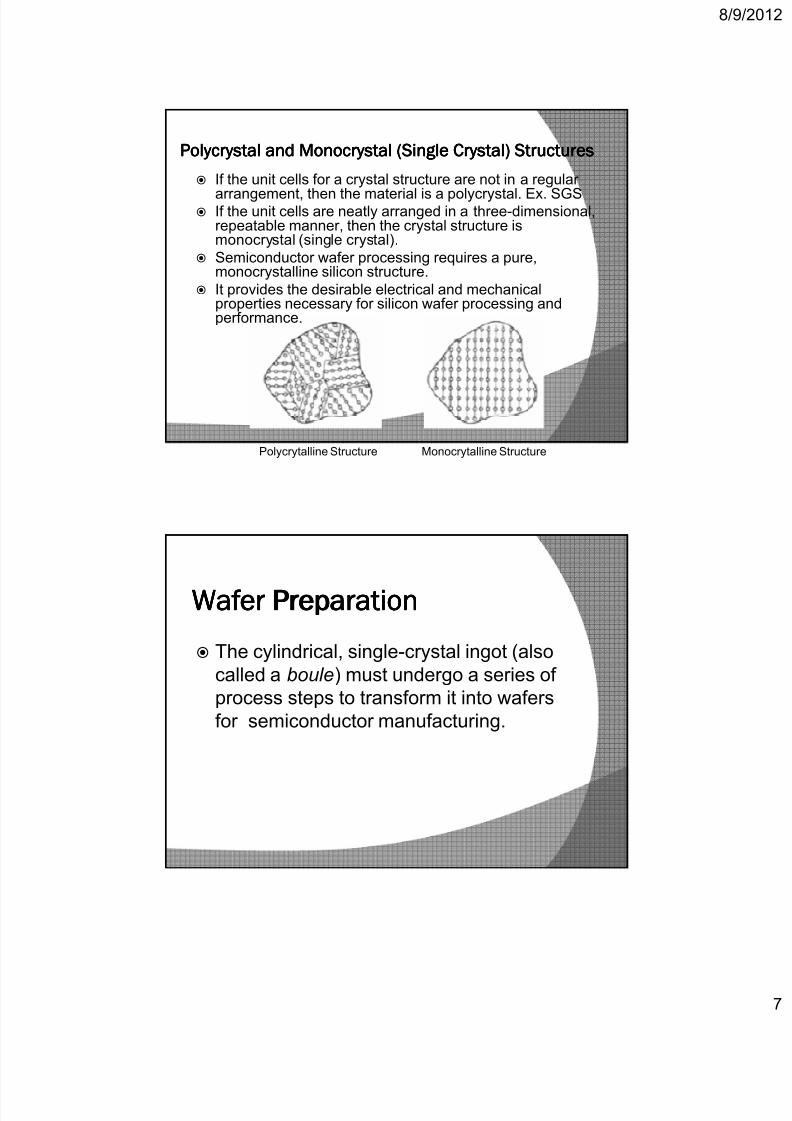
7212019 EE503 Topic 2 Hoo
httpslidepdfcomreaderfullee503-topic-2-hoo 822
89
Crystal growth is the process of converting
the polysilicon chunks of semiconductor-
grade silicon into a large monocrystal of
silicon
Over 85 of all silicon crystals are grown
according to the Czochralski (CZ) method
The Czochralski growth of a silicon
monocrystal involves the transformation of
molten SG silicon liquid into a solid silicon
ingot
SINGLE CRYSTAL SILICON GROWTHSINGLE CRYSTAL SILICON GROWTHSINGLE CRYSTAL SILICON GROWTHSINGLE CRYSTAL SILICON GROWTH
7212019 EE503 Topic 2 Hoo
httpslidepdfcomreaderfullee503-topic-2-hoo 922
89
To grow a silicon ingot chunks of SG silicon(polycrystal) are placed in a quartz crucible alongwith small amounts of dopant (boron to create p-typesilicon phosphorus to make n-type silicon)
The crucible of silicon is heated in the furnace usingheating elements
Czochralski (CZ) methodCzochralski (CZ) methodCzochralski (CZ) methodCzochralski (CZ) method
A crystal seed is attached to a crsytal pullermechanism
The seed is placed at the surface of the melt and isslowly drawn away while rotating in a direction that isopposite to the rotation of the crucible
Liquid from the melt is raised with it by surfacetension and slowly solidifies downward
As the seed is steadily pulled out of the melt androtated a single crystal ingot formed
7212019 EE503 Topic 2 Hoo
httpslidepdfcomreaderfullee503-topic-2-hoo 1022
89
FloatFloatFloatFloat----Zone (FZ) MethodZone (FZ) MethodZone (FZ) MethodZone (FZ) Method
A bar of doped polycrystal is
placed in the grower A monocrystal seed is attached
to one end of the bar
An RF coil applies heat at thecontact area of the bar and seedfor about 30 minutes
This monocrystal (single crystal)growth process progresses alongthe bar as the heater is movedalong its axis
FZ method produces high-puritysilicon with lower oxygen contentcrystals
FZ typically makes smaller-diameter wafers than the CZprocess
Crystal Trimming amp Diameter GrindCrystal Trimming amp Diameter GrindCrystal Trimming amp Diameter GrindCrystal Trimming amp Diameter Grind
End Removal
to cropped off the two ends of the ingot
check dopant uniformity throughout the
ingot
Diameter Grinding
to create precise diameter control and
roundness of the ingot
Critical for automated wafer-handling steps
in wafer fabs
7212019 EE503 Topic 2 Hoo
httpslidepdfcomreaderfullee503-topic-2-hoo 1122
89
Flat Grinding Flat Grinding Flat Grinding Flat Grinding Wafer Flat - to identify the crystal structure and to orient the wafer
Wafer SlicingWafer SlicingWafer SlicingWafer Slicing Slicing of wafer is being done with an
Internal Diameter Saw or Wire Saw
The thickness of the wafer is carefully
controlled at 75 plusmn 25 microns
Wafer thickness is crucial to withstand
high temperature and mechanical
shocks during semiconductor fabrication
process
Wafer Lapping Wafer Lapping Wafer Lapping Wafer Lapping a mechanical two-sided lapping operation to
remove damage left by slicing and to achieve
a high degree of parallelism and flatness of
the wafer
Edge ContourRounding Edge ContourRounding Edge ContourRounding Edge ContourRounding A polished wafer edge grind is applied to the
wafer to contour a smooth radius on the edge of
the wafer
before or after lapping
A smooth edge radius is important to minimize
chipped edges which cause edge dislocation
growth during thermal process
7212019 EE503 Topic 2 Hoo
httpslidepdfcomreaderfullee503-topic-2-hoo 1222
89
EtchingEtchingEtchingEtching Wafers undergo a wet chemical etch process to
remove the damage and contamination on thewafer
about 20 microns of silicon wafer surface is
removed to ensure that all damage is removed
PolishingPolishingPolishingPolishing Double-sided Polishing (DSP) with Chemical
Mechanical Planarization (CMP) to achieve a
smooth wafer surface with a high degree offlatness
Wafer InspectionEvaluationWafer InspectionEvaluationWafer InspectionEvaluationWafer InspectionEvaluation Prior to packaging the wafer it is inspected for
quality criteria that are specified by the customer
Ex surface defects such as particulate
contamination and stains
7212019 EE503 Topic 2 Hoo
httpslidepdfcomreaderfullee503-topic-2-hoo 1322
89
Epitaxial LayerEpitaxial LayerEpitaxial LayerEpitaxial LayerEpitaxial LayerEpitaxial LayerEpitaxial LayerEpitaxial Layer
Epitaxial layer (also known as epilayer ) A layer of the same monocrystalline structure deposited on
the surface of the silicon wafer with control over the
doping type or concentration
Thickness 05 to 5 microm
Ex n-type epilayer on a p-type wafer
Ex p-type epilayer (low concentration ) on a p-type wafer
Importance of Epitaxial LayerImportance of Epitaxial LayerImportance of Epitaxial LayerImportance of Epitaxial LayerImportance of Epitaxial LayerImportance of Epitaxial LayerImportance of Epitaxial LayerImportance of Epitaxial Layer
To improve performance in bipolar transistors and
integrated circuits
Bipolar transistors - high breakdown voltage in the pn
junction low collector resistance high speed at
moderate currents
CMOS ICs - minimizes latchup problems
7212019 EE503 Topic 2 Hoo
httpslidepdfcomreaderfullee503-topic-2-hoo 1422
89
Epitaxial Growth MethodsEpitaxial Growth MethodsEpitaxial Growth MethodsEpitaxial Growth MethodsEpitaxial Growth MethodsEpitaxial Growth MethodsEpitaxial Growth MethodsEpitaxial Growth Methods
Three methods used to grow epitaxial
layers on silicon wafers for IC production
are
1 Vapor-phase epitaxy (VPE)
2 Metalorganic CVD (MOCVD)
3 Molecular-beam epitaxy (MBE)
VaporVaporVaporVapor----Phase Epitaxy (VPE)Phase Epitaxy (VPE)Phase Epitaxy (VPE)Phase Epitaxy (VPE) The most common method used for silicon epitaxial
growth
Silicon VPE is achieved by passing gas compounds of
the desired chemicals over single-crystal silicon wafers
that are heated from 800 to 1150degC
The heat from the high temperature provides the
energy necessary to drive the chemical reactions
which take place on the surface of the wafer
7212019 EE503 Topic 2 Hoo
httpslidepdfcomreaderfullee503-topic-2-hoo 1522
89
Metalorganic CVD (MOCVD)
MOCVD is a form of VPE
at low temperature
As with the VPE process compounds of the desired
materials are transported to a heated substrate where
the complex chemical reaction takes place on the wafer
surface
not typically used for silicon epitaxy
important for the controlled deposition of ultra-thin
doped or undoped semiconductor such as gallium
arsenide (GaAs) primarily used for lasers light-emittingdiodes (LED)
MolecularMolecularMolecularMolecular----Beam Epitaxy (MBE)Beam Epitaxy (MBE)Beam Epitaxy (MBE)Beam Epitaxy (MBE)
MBE takes place under conditions of high vacuum
temperature range is between 500 to 900degC
Most silicon MBE systems produce silicon atoms for the
epitaxial reaction through the evaporation of silicon with
an electromagnetically focused electron beam source
The beam of silicon atoms leaving the silicon source
travels through the evacuated chamber without
collisions and deposits on the single-crystal wafersurface
7212019 EE503 Topic 2 Hoo
httpslidepdfcomreaderfullee503-topic-2-hoo 1622
89
Characteristics of wafer for IC FabricationCharacteristics of wafer for IC FabricationCharacteristics of wafer for IC FabricationCharacteristics of wafer for IC FabricationCharacteristics of wafer for IC FabricationCharacteristics of wafer for IC FabricationCharacteristics of wafer for IC FabricationCharacteristics of wafer for IC Fabrication
Important silicon wafer quality requirements are
Physical dimensions
Flatness
Microroughness
Oxygen content
Crystal defects
Particles
Bulk resistivity
The suppliers of silicon wafers must control their
wafer quality by performing ingot and waferquality inspections to demonstrate that quality
specifications are met
Physical Dimensions measurements such as diameter thickness
location and size of orientation flat (or notch) and
wafer deformation
Flatness
most critical wafer parameters because of
photolithography process
Wafer flatness is the linear thickness variation
across the wafer
Typical flatness specifications for site flatness are
008 to 012microm
7212019 EE503 Topic 2 Hoo
httpslidepdfcomreaderfullee503-topic-2-hoo 1722
89
Microroughness
Surface microroughness measures the peaks and valleys height
deviation on the wafer surface and is specified in units of
nanometers
Surface microroughness is important to avoid breakdown of very
thin dielectric films during device fabrication
Wafers undergo a lapping step followed by an etching step to
remove surface microroughness
Oxygen Content
Small amounts of oxygen can have beneficial gettering effects
which can tie up contaminants in the wafer
However excessive oxygen in the silicon ingot can affect the
mechanical and electrical properties of the silicon
increase in the leakage current at the pn junction and also to
increased MOS leakage
Crystal Defects the current requirement is for the number of
crystal defects per square centimeter to be less
than 1000
Particles
The number of surface particles are controlled on
a wafer to minimize yield loss during wafer
fabrication
minimize the generation of particles during wafer
processing followed by effective cleaning stepsto remove particles
A typical wafer-cleanliness specification is to have
less than 013 particles per square centimeter
(1300 particles per square meter) of wafer
surface area on a 200-mm wafer
7212019 EE503 Topic 2 Hoo
httpslidepdfcomreaderfullee503-topic-2-hoo 1822
89
Bulk Resistivity
The resistivity of the bulk silicon ingot depends on
the density of the dopant material that was addedto the silicon melt prior to crystal growth
Adding dopants to silicon is to decrease its
resistivity due to increased carrier mobility
During crystal growth process different
temperature at the center of the ingot and
decreases toward the outer edge produces
variations in the radial doping concentration of the
ingot
The bulk silicon ingot is checked for correctresistivity and uniformity after the ends of the ingot
have been removed
Reasons For Larger Ingot DiametersReasons For Larger Ingot DiametersReasons For Larger Ingot DiametersReasons For Larger Ingot Diameters
Silicon ingot diameters have increased from less than
25 mm (1950s) to 300 mm (recent)
The main reason for increasing ingot diameter is due to
wafer fabrication cost
Larger-diameter wafers have a greater surface area for
chips More chips that can be produced from a single
wafer
7212019 EE503 Topic 2 Hoo
httpslidepdfcomreaderfullee503-topic-2-hoo 1922
89
Larger wafers means more chips per wafer leading to
improved equipment productivity due to economies of
scale for less handling per chip and less processing
time per chip It is estimated that conversion to a 300-mm wafer diameter will reduce the fabrication cost per
chip by approximately 30 through equipment
utilization improvements
Another benefit from larger-diameter wafers is that fewer
chips are near the edge of the wafer which translates
into higher production yield
Ultimately cost savings will be the major factor that
drives the industry toward a larger wafer diameter
Sources of Contamination
Seven sources of contamination in a wafer
fabrication facility are
1 Air
2 Humans
3 Facility
4 Water
5 Process chemicals
6 Process gases
7 Production equipment
7212019 EE503 Topic 2 Hoo
httpslidepdfcomreaderfullee503-topic-2-hoo 2022
89
1 Air
The most fundamental concept of a cleanroom is the
control of particles in the wafer fab air small airborne aerosol particles float and remain in the
air depositing on wafers as contamination and
creating killer defects
2 Humans
People are the greatest sources of contamination in a
cleanroom
Particles come from hair clothes dead skin
excessive movements talking coughing and
sneezing are damaging to semiconductors
Average person sheds over 10000000 particles perminute of 03 microm size and larger
Require cleanroom garment
3 Facility3 Facility3 Facility3 Facility
A simplified diagram of the air handling system in a wafer
fab cleanroom
7212019 EE503 Topic 2 Hoo
httpslidepdfcomreaderfullee503-topic-2-hoo 2122
89
Air Filtering
Air enters the cleanroom through special particulate filters
in the ceiling and passes with laminar flow to the floorand into the recirculation air system to return back to the
air filtering system with makeup air An exhaust system
is used to remove undesirable heat and chemicals
Temperature and Humidity
temperature control in a class 1 at 03 microm cleanroom is
68 plusmn 05deg
Relative humidity (RH) 40 +-10 - important because
of its contribution toward corrosion
Electrostatic Discharge Static-dissipative cleanroom
materials ESD grounding Air ionization
3 Water To manufacture semiconductors a high quality
ultrapure deionized (DI) water (sometimes referred
to as UPW) is required primarily in the chemical
wafer cleaning solutions and as a postclean rinse
Free from Dissolved ions Organic materials
Particulates Bacteria Silica and Dissolved oxygen
4 Process Chemicals Process Gases
Liquid chemicals used in semiconductor processing
must be free of contamination for successful device
yield and performance Filters are used to prevent chemical degradation
during delivery or to maintain chemical purity
during a recirculation step
Gases pass through purifiers and gas filters to
remove impurities and particles
7212019 EE503 Topic 2 Hoo
httpslidepdfcomreaderfullee503-topic-2-hoo 2222
89
5 Production Equipment Many wafer fabrication operations occur in a
vacuum which requires special design
considerations to avoid contamination
Since equipment automation means fewer
humans interacting with the product there is
less concern about particles from humans and
more emphasis on reducing particles from
equipment
CleanroomCleanroomCleanroomCleanroom The class number designates the air quality inside a
cleanroom by defining the particle size and density in
the cleanroom air
US Federal Standard 209E Examples
Class 10 at 02 microm - a maximum of 75 particles per
cubic foot at 02 microm or larger
Class 10 at 01 microm - a maximum of 350 particles per
cubic foot at 01 microm or larger
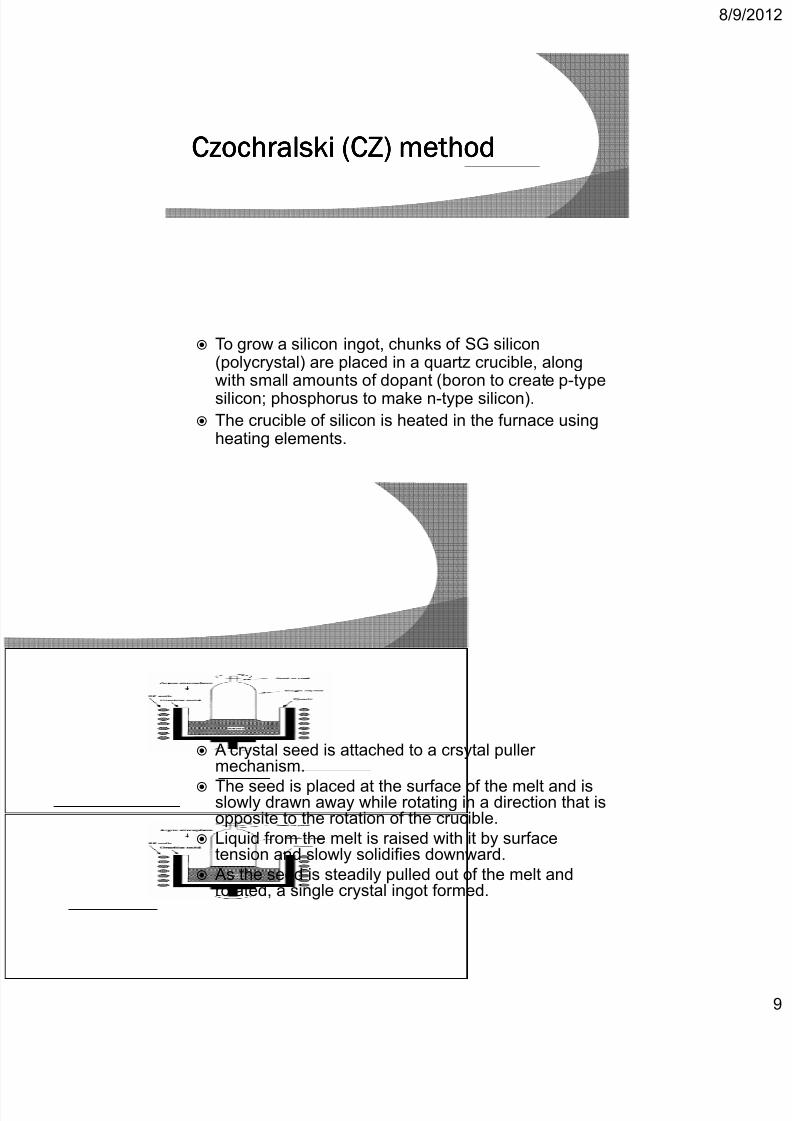
7212019 EE503 Topic 2 Hoo
httpslidepdfcomreaderfullee503-topic-2-hoo 922
89
To grow a silicon ingot chunks of SG silicon(polycrystal) are placed in a quartz crucible alongwith small amounts of dopant (boron to create p-typesilicon phosphorus to make n-type silicon)
The crucible of silicon is heated in the furnace usingheating elements
Czochralski (CZ) methodCzochralski (CZ) methodCzochralski (CZ) methodCzochralski (CZ) method
A crystal seed is attached to a crsytal pullermechanism
The seed is placed at the surface of the melt and isslowly drawn away while rotating in a direction that isopposite to the rotation of the crucible
Liquid from the melt is raised with it by surfacetension and slowly solidifies downward
As the seed is steadily pulled out of the melt androtated a single crystal ingot formed
7212019 EE503 Topic 2 Hoo
httpslidepdfcomreaderfullee503-topic-2-hoo 1022
89
FloatFloatFloatFloat----Zone (FZ) MethodZone (FZ) MethodZone (FZ) MethodZone (FZ) Method
A bar of doped polycrystal is
placed in the grower A monocrystal seed is attached
to one end of the bar
An RF coil applies heat at thecontact area of the bar and seedfor about 30 minutes
This monocrystal (single crystal)growth process progresses alongthe bar as the heater is movedalong its axis
FZ method produces high-puritysilicon with lower oxygen contentcrystals
FZ typically makes smaller-diameter wafers than the CZprocess
Crystal Trimming amp Diameter GrindCrystal Trimming amp Diameter GrindCrystal Trimming amp Diameter GrindCrystal Trimming amp Diameter Grind
End Removal
to cropped off the two ends of the ingot
check dopant uniformity throughout the
ingot
Diameter Grinding
to create precise diameter control and
roundness of the ingot
Critical for automated wafer-handling steps
in wafer fabs
7212019 EE503 Topic 2 Hoo
httpslidepdfcomreaderfullee503-topic-2-hoo 1122
89
Flat Grinding Flat Grinding Flat Grinding Flat Grinding Wafer Flat - to identify the crystal structure and to orient the wafer
Wafer SlicingWafer SlicingWafer SlicingWafer Slicing Slicing of wafer is being done with an
Internal Diameter Saw or Wire Saw
The thickness of the wafer is carefully
controlled at 75 plusmn 25 microns
Wafer thickness is crucial to withstand
high temperature and mechanical
shocks during semiconductor fabrication
process
Wafer Lapping Wafer Lapping Wafer Lapping Wafer Lapping a mechanical two-sided lapping operation to
remove damage left by slicing and to achieve
a high degree of parallelism and flatness of
the wafer
Edge ContourRounding Edge ContourRounding Edge ContourRounding Edge ContourRounding A polished wafer edge grind is applied to the
wafer to contour a smooth radius on the edge of
the wafer
before or after lapping
A smooth edge radius is important to minimize
chipped edges which cause edge dislocation
growth during thermal process
7212019 EE503 Topic 2 Hoo
httpslidepdfcomreaderfullee503-topic-2-hoo 1222
89
EtchingEtchingEtchingEtching Wafers undergo a wet chemical etch process to
remove the damage and contamination on thewafer
about 20 microns of silicon wafer surface is
removed to ensure that all damage is removed
PolishingPolishingPolishingPolishing Double-sided Polishing (DSP) with Chemical
Mechanical Planarization (CMP) to achieve a
smooth wafer surface with a high degree offlatness
Wafer InspectionEvaluationWafer InspectionEvaluationWafer InspectionEvaluationWafer InspectionEvaluation Prior to packaging the wafer it is inspected for
quality criteria that are specified by the customer
Ex surface defects such as particulate
contamination and stains
7212019 EE503 Topic 2 Hoo
httpslidepdfcomreaderfullee503-topic-2-hoo 1322
89
Epitaxial LayerEpitaxial LayerEpitaxial LayerEpitaxial LayerEpitaxial LayerEpitaxial LayerEpitaxial LayerEpitaxial Layer
Epitaxial layer (also known as epilayer ) A layer of the same monocrystalline structure deposited on
the surface of the silicon wafer with control over the
doping type or concentration
Thickness 05 to 5 microm
Ex n-type epilayer on a p-type wafer
Ex p-type epilayer (low concentration ) on a p-type wafer
Importance of Epitaxial LayerImportance of Epitaxial LayerImportance of Epitaxial LayerImportance of Epitaxial LayerImportance of Epitaxial LayerImportance of Epitaxial LayerImportance of Epitaxial LayerImportance of Epitaxial Layer
To improve performance in bipolar transistors and
integrated circuits
Bipolar transistors - high breakdown voltage in the pn
junction low collector resistance high speed at
moderate currents
CMOS ICs - minimizes latchup problems
7212019 EE503 Topic 2 Hoo
httpslidepdfcomreaderfullee503-topic-2-hoo 1422
89
Epitaxial Growth MethodsEpitaxial Growth MethodsEpitaxial Growth MethodsEpitaxial Growth MethodsEpitaxial Growth MethodsEpitaxial Growth MethodsEpitaxial Growth MethodsEpitaxial Growth Methods
Three methods used to grow epitaxial
layers on silicon wafers for IC production
are
1 Vapor-phase epitaxy (VPE)
2 Metalorganic CVD (MOCVD)
3 Molecular-beam epitaxy (MBE)
VaporVaporVaporVapor----Phase Epitaxy (VPE)Phase Epitaxy (VPE)Phase Epitaxy (VPE)Phase Epitaxy (VPE) The most common method used for silicon epitaxial
growth
Silicon VPE is achieved by passing gas compounds of
the desired chemicals over single-crystal silicon wafers
that are heated from 800 to 1150degC
The heat from the high temperature provides the
energy necessary to drive the chemical reactions
which take place on the surface of the wafer
7212019 EE503 Topic 2 Hoo
httpslidepdfcomreaderfullee503-topic-2-hoo 1522
89
Metalorganic CVD (MOCVD)
MOCVD is a form of VPE
at low temperature
As with the VPE process compounds of the desired
materials are transported to a heated substrate where
the complex chemical reaction takes place on the wafer
surface
not typically used for silicon epitaxy
important for the controlled deposition of ultra-thin
doped or undoped semiconductor such as gallium
arsenide (GaAs) primarily used for lasers light-emittingdiodes (LED)
MolecularMolecularMolecularMolecular----Beam Epitaxy (MBE)Beam Epitaxy (MBE)Beam Epitaxy (MBE)Beam Epitaxy (MBE)
MBE takes place under conditions of high vacuum
temperature range is between 500 to 900degC
Most silicon MBE systems produce silicon atoms for the
epitaxial reaction through the evaporation of silicon with
an electromagnetically focused electron beam source
The beam of silicon atoms leaving the silicon source
travels through the evacuated chamber without
collisions and deposits on the single-crystal wafersurface
7212019 EE503 Topic 2 Hoo
httpslidepdfcomreaderfullee503-topic-2-hoo 1622
89
Characteristics of wafer for IC FabricationCharacteristics of wafer for IC FabricationCharacteristics of wafer for IC FabricationCharacteristics of wafer for IC FabricationCharacteristics of wafer for IC FabricationCharacteristics of wafer for IC FabricationCharacteristics of wafer for IC FabricationCharacteristics of wafer for IC Fabrication
Important silicon wafer quality requirements are
Physical dimensions
Flatness
Microroughness
Oxygen content
Crystal defects
Particles
Bulk resistivity
The suppliers of silicon wafers must control their
wafer quality by performing ingot and waferquality inspections to demonstrate that quality
specifications are met
Physical Dimensions measurements such as diameter thickness
location and size of orientation flat (or notch) and
wafer deformation
Flatness
most critical wafer parameters because of
photolithography process
Wafer flatness is the linear thickness variation
across the wafer
Typical flatness specifications for site flatness are
008 to 012microm
7212019 EE503 Topic 2 Hoo
httpslidepdfcomreaderfullee503-topic-2-hoo 1722
89
Microroughness
Surface microroughness measures the peaks and valleys height
deviation on the wafer surface and is specified in units of
nanometers
Surface microroughness is important to avoid breakdown of very
thin dielectric films during device fabrication
Wafers undergo a lapping step followed by an etching step to
remove surface microroughness
Oxygen Content
Small amounts of oxygen can have beneficial gettering effects
which can tie up contaminants in the wafer
However excessive oxygen in the silicon ingot can affect the
mechanical and electrical properties of the silicon
increase in the leakage current at the pn junction and also to
increased MOS leakage
Crystal Defects the current requirement is for the number of
crystal defects per square centimeter to be less
than 1000
Particles
The number of surface particles are controlled on
a wafer to minimize yield loss during wafer
fabrication
minimize the generation of particles during wafer
processing followed by effective cleaning stepsto remove particles
A typical wafer-cleanliness specification is to have
less than 013 particles per square centimeter
(1300 particles per square meter) of wafer
surface area on a 200-mm wafer
7212019 EE503 Topic 2 Hoo
httpslidepdfcomreaderfullee503-topic-2-hoo 1822
89
Bulk Resistivity
The resistivity of the bulk silicon ingot depends on
the density of the dopant material that was addedto the silicon melt prior to crystal growth
Adding dopants to silicon is to decrease its
resistivity due to increased carrier mobility
During crystal growth process different
temperature at the center of the ingot and
decreases toward the outer edge produces
variations in the radial doping concentration of the
ingot
The bulk silicon ingot is checked for correctresistivity and uniformity after the ends of the ingot
have been removed
Reasons For Larger Ingot DiametersReasons For Larger Ingot DiametersReasons For Larger Ingot DiametersReasons For Larger Ingot Diameters
Silicon ingot diameters have increased from less than
25 mm (1950s) to 300 mm (recent)
The main reason for increasing ingot diameter is due to
wafer fabrication cost
Larger-diameter wafers have a greater surface area for
chips More chips that can be produced from a single
wafer
7212019 EE503 Topic 2 Hoo
httpslidepdfcomreaderfullee503-topic-2-hoo 1922
89
Larger wafers means more chips per wafer leading to
improved equipment productivity due to economies of
scale for less handling per chip and less processing
time per chip It is estimated that conversion to a 300-mm wafer diameter will reduce the fabrication cost per
chip by approximately 30 through equipment
utilization improvements
Another benefit from larger-diameter wafers is that fewer
chips are near the edge of the wafer which translates
into higher production yield
Ultimately cost savings will be the major factor that
drives the industry toward a larger wafer diameter
Sources of Contamination
Seven sources of contamination in a wafer
fabrication facility are
1 Air
2 Humans
3 Facility
4 Water
5 Process chemicals
6 Process gases
7 Production equipment
7212019 EE503 Topic 2 Hoo
httpslidepdfcomreaderfullee503-topic-2-hoo 2022
89
1 Air
The most fundamental concept of a cleanroom is the
control of particles in the wafer fab air small airborne aerosol particles float and remain in the
air depositing on wafers as contamination and
creating killer defects
2 Humans
People are the greatest sources of contamination in a
cleanroom
Particles come from hair clothes dead skin
excessive movements talking coughing and
sneezing are damaging to semiconductors
Average person sheds over 10000000 particles perminute of 03 microm size and larger
Require cleanroom garment
3 Facility3 Facility3 Facility3 Facility
A simplified diagram of the air handling system in a wafer
fab cleanroom
7212019 EE503 Topic 2 Hoo
httpslidepdfcomreaderfullee503-topic-2-hoo 2122
89
Air Filtering
Air enters the cleanroom through special particulate filters
in the ceiling and passes with laminar flow to the floorand into the recirculation air system to return back to the
air filtering system with makeup air An exhaust system
is used to remove undesirable heat and chemicals
Temperature and Humidity
temperature control in a class 1 at 03 microm cleanroom is
68 plusmn 05deg
Relative humidity (RH) 40 +-10 - important because
of its contribution toward corrosion
Electrostatic Discharge Static-dissipative cleanroom
materials ESD grounding Air ionization
3 Water To manufacture semiconductors a high quality
ultrapure deionized (DI) water (sometimes referred
to as UPW) is required primarily in the chemical
wafer cleaning solutions and as a postclean rinse
Free from Dissolved ions Organic materials
Particulates Bacteria Silica and Dissolved oxygen
4 Process Chemicals Process Gases
Liquid chemicals used in semiconductor processing
must be free of contamination for successful device
yield and performance Filters are used to prevent chemical degradation
during delivery or to maintain chemical purity
during a recirculation step
Gases pass through purifiers and gas filters to
remove impurities and particles
7212019 EE503 Topic 2 Hoo
httpslidepdfcomreaderfullee503-topic-2-hoo 2222
89
5 Production Equipment Many wafer fabrication operations occur in a
vacuum which requires special design
considerations to avoid contamination
Since equipment automation means fewer
humans interacting with the product there is
less concern about particles from humans and
more emphasis on reducing particles from
equipment
CleanroomCleanroomCleanroomCleanroom The class number designates the air quality inside a
cleanroom by defining the particle size and density in
the cleanroom air
US Federal Standard 209E Examples
Class 10 at 02 microm - a maximum of 75 particles per
cubic foot at 02 microm or larger
Class 10 at 01 microm - a maximum of 350 particles per
cubic foot at 01 microm or larger
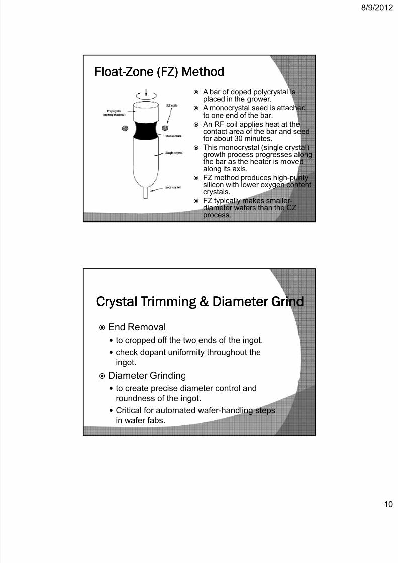
7212019 EE503 Topic 2 Hoo
httpslidepdfcomreaderfullee503-topic-2-hoo 1222
89
EtchingEtchingEtchingEtching Wafers undergo a wet chemical etch process to
remove the damage and contamination on thewafer
about 20 microns of silicon wafer surface is
removed to ensure that all damage is removed
PolishingPolishingPolishingPolishing Double-sided Polishing (DSP) with Chemical
Mechanical Planarization (CMP) to achieve a
smooth wafer surface with a high degree offlatness
Wafer InspectionEvaluationWafer InspectionEvaluationWafer InspectionEvaluationWafer InspectionEvaluation Prior to packaging the wafer it is inspected for
quality criteria that are specified by the customer
Ex surface defects such as particulate
contamination and stains
7212019 EE503 Topic 2 Hoo
httpslidepdfcomreaderfullee503-topic-2-hoo 1322
89
Epitaxial LayerEpitaxial LayerEpitaxial LayerEpitaxial LayerEpitaxial LayerEpitaxial LayerEpitaxial LayerEpitaxial Layer
Epitaxial layer (also known as epilayer ) A layer of the same monocrystalline structure deposited on
the surface of the silicon wafer with control over the
doping type or concentration
Thickness 05 to 5 microm
Ex n-type epilayer on a p-type wafer
Ex p-type epilayer (low concentration ) on a p-type wafer
Importance of Epitaxial LayerImportance of Epitaxial LayerImportance of Epitaxial LayerImportance of Epitaxial LayerImportance of Epitaxial LayerImportance of Epitaxial LayerImportance of Epitaxial LayerImportance of Epitaxial Layer
To improve performance in bipolar transistors and
integrated circuits
Bipolar transistors - high breakdown voltage in the pn
junction low collector resistance high speed at
moderate currents
CMOS ICs - minimizes latchup problems
7212019 EE503 Topic 2 Hoo
httpslidepdfcomreaderfullee503-topic-2-hoo 1422
89
Epitaxial Growth MethodsEpitaxial Growth MethodsEpitaxial Growth MethodsEpitaxial Growth MethodsEpitaxial Growth MethodsEpitaxial Growth MethodsEpitaxial Growth MethodsEpitaxial Growth Methods
Three methods used to grow epitaxial
layers on silicon wafers for IC production
are
1 Vapor-phase epitaxy (VPE)
2 Metalorganic CVD (MOCVD)
3 Molecular-beam epitaxy (MBE)
VaporVaporVaporVapor----Phase Epitaxy (VPE)Phase Epitaxy (VPE)Phase Epitaxy (VPE)Phase Epitaxy (VPE) The most common method used for silicon epitaxial
growth
Silicon VPE is achieved by passing gas compounds of
the desired chemicals over single-crystal silicon wafers
that are heated from 800 to 1150degC
The heat from the high temperature provides the
energy necessary to drive the chemical reactions
which take place on the surface of the wafer
7212019 EE503 Topic 2 Hoo
httpslidepdfcomreaderfullee503-topic-2-hoo 1522
89
Metalorganic CVD (MOCVD)
MOCVD is a form of VPE
at low temperature
As with the VPE process compounds of the desired
materials are transported to a heated substrate where
the complex chemical reaction takes place on the wafer
surface
not typically used for silicon epitaxy
important for the controlled deposition of ultra-thin
doped or undoped semiconductor such as gallium
arsenide (GaAs) primarily used for lasers light-emittingdiodes (LED)
MolecularMolecularMolecularMolecular----Beam Epitaxy (MBE)Beam Epitaxy (MBE)Beam Epitaxy (MBE)Beam Epitaxy (MBE)
MBE takes place under conditions of high vacuum
temperature range is between 500 to 900degC
Most silicon MBE systems produce silicon atoms for the
epitaxial reaction through the evaporation of silicon with
an electromagnetically focused electron beam source
The beam of silicon atoms leaving the silicon source
travels through the evacuated chamber without
collisions and deposits on the single-crystal wafersurface
7212019 EE503 Topic 2 Hoo
httpslidepdfcomreaderfullee503-topic-2-hoo 1622
89
Characteristics of wafer for IC FabricationCharacteristics of wafer for IC FabricationCharacteristics of wafer for IC FabricationCharacteristics of wafer for IC FabricationCharacteristics of wafer for IC FabricationCharacteristics of wafer for IC FabricationCharacteristics of wafer for IC FabricationCharacteristics of wafer for IC Fabrication
Important silicon wafer quality requirements are
Physical dimensions
Flatness
Microroughness
Oxygen content
Crystal defects
Particles
Bulk resistivity
The suppliers of silicon wafers must control their
wafer quality by performing ingot and waferquality inspections to demonstrate that quality
specifications are met
Physical Dimensions measurements such as diameter thickness
location and size of orientation flat (or notch) and
wafer deformation
Flatness
most critical wafer parameters because of
photolithography process
Wafer flatness is the linear thickness variation
across the wafer
Typical flatness specifications for site flatness are
008 to 012microm
7212019 EE503 Topic 2 Hoo
httpslidepdfcomreaderfullee503-topic-2-hoo 1722
89
Microroughness
Surface microroughness measures the peaks and valleys height
deviation on the wafer surface and is specified in units of
nanometers
Surface microroughness is important to avoid breakdown of very
thin dielectric films during device fabrication
Wafers undergo a lapping step followed by an etching step to
remove surface microroughness
Oxygen Content
Small amounts of oxygen can have beneficial gettering effects
which can tie up contaminants in the wafer
However excessive oxygen in the silicon ingot can affect the
mechanical and electrical properties of the silicon
increase in the leakage current at the pn junction and also to
increased MOS leakage
Crystal Defects the current requirement is for the number of
crystal defects per square centimeter to be less
than 1000
Particles
The number of surface particles are controlled on
a wafer to minimize yield loss during wafer
fabrication
minimize the generation of particles during wafer
processing followed by effective cleaning stepsto remove particles
A typical wafer-cleanliness specification is to have
less than 013 particles per square centimeter
(1300 particles per square meter) of wafer
surface area on a 200-mm wafer
7212019 EE503 Topic 2 Hoo
httpslidepdfcomreaderfullee503-topic-2-hoo 1822
89
Bulk Resistivity
The resistivity of the bulk silicon ingot depends on
the density of the dopant material that was addedto the silicon melt prior to crystal growth
Adding dopants to silicon is to decrease its
resistivity due to increased carrier mobility
During crystal growth process different
temperature at the center of the ingot and
decreases toward the outer edge produces
variations in the radial doping concentration of the
ingot
The bulk silicon ingot is checked for correctresistivity and uniformity after the ends of the ingot
have been removed
Reasons For Larger Ingot DiametersReasons For Larger Ingot DiametersReasons For Larger Ingot DiametersReasons For Larger Ingot Diameters
Silicon ingot diameters have increased from less than
25 mm (1950s) to 300 mm (recent)
The main reason for increasing ingot diameter is due to
wafer fabrication cost
Larger-diameter wafers have a greater surface area for
chips More chips that can be produced from a single
wafer
7212019 EE503 Topic 2 Hoo
httpslidepdfcomreaderfullee503-topic-2-hoo 1922
89
Larger wafers means more chips per wafer leading to
improved equipment productivity due to economies of
scale for less handling per chip and less processing
time per chip It is estimated that conversion to a 300-mm wafer diameter will reduce the fabrication cost per
chip by approximately 30 through equipment
utilization improvements
Another benefit from larger-diameter wafers is that fewer
chips are near the edge of the wafer which translates
into higher production yield
Ultimately cost savings will be the major factor that
drives the industry toward a larger wafer diameter
Sources of Contamination
Seven sources of contamination in a wafer
fabrication facility are
1 Air
2 Humans
3 Facility
4 Water
5 Process chemicals
6 Process gases
7 Production equipment
7212019 EE503 Topic 2 Hoo
httpslidepdfcomreaderfullee503-topic-2-hoo 2022
89
1 Air
The most fundamental concept of a cleanroom is the
control of particles in the wafer fab air small airborne aerosol particles float and remain in the
air depositing on wafers as contamination and
creating killer defects
2 Humans
People are the greatest sources of contamination in a
cleanroom
Particles come from hair clothes dead skin
excessive movements talking coughing and
sneezing are damaging to semiconductors
Average person sheds over 10000000 particles perminute of 03 microm size and larger
Require cleanroom garment
3 Facility3 Facility3 Facility3 Facility
A simplified diagram of the air handling system in a wafer
fab cleanroom
7212019 EE503 Topic 2 Hoo
httpslidepdfcomreaderfullee503-topic-2-hoo 2122
89
Air Filtering
Air enters the cleanroom through special particulate filters
in the ceiling and passes with laminar flow to the floorand into the recirculation air system to return back to the
air filtering system with makeup air An exhaust system
is used to remove undesirable heat and chemicals
Temperature and Humidity
temperature control in a class 1 at 03 microm cleanroom is
68 plusmn 05deg
Relative humidity (RH) 40 +-10 - important because
of its contribution toward corrosion
Electrostatic Discharge Static-dissipative cleanroom
materials ESD grounding Air ionization
3 Water To manufacture semiconductors a high quality
ultrapure deionized (DI) water (sometimes referred
to as UPW) is required primarily in the chemical
wafer cleaning solutions and as a postclean rinse
Free from Dissolved ions Organic materials
Particulates Bacteria Silica and Dissolved oxygen
4 Process Chemicals Process Gases
Liquid chemicals used in semiconductor processing
must be free of contamination for successful device
yield and performance Filters are used to prevent chemical degradation
during delivery or to maintain chemical purity
during a recirculation step
Gases pass through purifiers and gas filters to
remove impurities and particles
7212019 EE503 Topic 2 Hoo
httpslidepdfcomreaderfullee503-topic-2-hoo 2222
89
5 Production Equipment Many wafer fabrication operations occur in a
vacuum which requires special design
considerations to avoid contamination
Since equipment automation means fewer
humans interacting with the product there is
less concern about particles from humans and
more emphasis on reducing particles from
equipment
CleanroomCleanroomCleanroomCleanroom The class number designates the air quality inside a
cleanroom by defining the particle size and density in
the cleanroom air
US Federal Standard 209E Examples
Class 10 at 02 microm - a maximum of 75 particles per
cubic foot at 02 microm or larger
Class 10 at 01 microm - a maximum of 350 particles per
cubic foot at 01 microm or larger
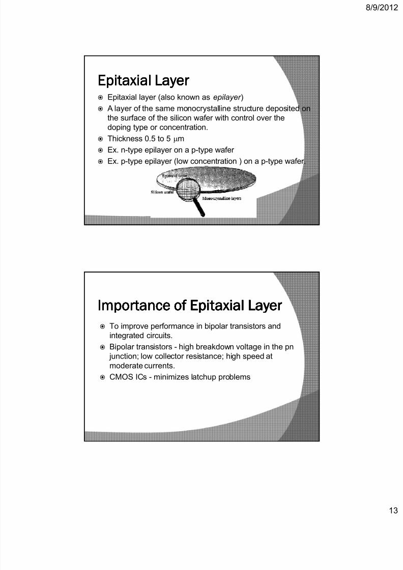
7212019 EE503 Topic 2 Hoo
httpslidepdfcomreaderfullee503-topic-2-hoo 1722
89
Microroughness
Surface microroughness measures the peaks and valleys height
deviation on the wafer surface and is specified in units of
nanometers
Surface microroughness is important to avoid breakdown of very
thin dielectric films during device fabrication
Wafers undergo a lapping step followed by an etching step to
remove surface microroughness
Oxygen Content
Small amounts of oxygen can have beneficial gettering effects
which can tie up contaminants in the wafer
However excessive oxygen in the silicon ingot can affect the
mechanical and electrical properties of the silicon
increase in the leakage current at the pn junction and also to
increased MOS leakage
Crystal Defects the current requirement is for the number of
crystal defects per square centimeter to be less
than 1000
Particles
The number of surface particles are controlled on
a wafer to minimize yield loss during wafer
fabrication
minimize the generation of particles during wafer
processing followed by effective cleaning stepsto remove particles
A typical wafer-cleanliness specification is to have
less than 013 particles per square centimeter
(1300 particles per square meter) of wafer
surface area on a 200-mm wafer
7212019 EE503 Topic 2 Hoo
httpslidepdfcomreaderfullee503-topic-2-hoo 1822
89
Bulk Resistivity
The resistivity of the bulk silicon ingot depends on
the density of the dopant material that was addedto the silicon melt prior to crystal growth
Adding dopants to silicon is to decrease its
resistivity due to increased carrier mobility
During crystal growth process different
temperature at the center of the ingot and
decreases toward the outer edge produces
variations in the radial doping concentration of the
ingot
The bulk silicon ingot is checked for correctresistivity and uniformity after the ends of the ingot
have been removed
Reasons For Larger Ingot DiametersReasons For Larger Ingot DiametersReasons For Larger Ingot DiametersReasons For Larger Ingot Diameters
Silicon ingot diameters have increased from less than
25 mm (1950s) to 300 mm (recent)
The main reason for increasing ingot diameter is due to
wafer fabrication cost
Larger-diameter wafers have a greater surface area for
chips More chips that can be produced from a single
wafer
7212019 EE503 Topic 2 Hoo
httpslidepdfcomreaderfullee503-topic-2-hoo 1922
89
Larger wafers means more chips per wafer leading to
improved equipment productivity due to economies of
scale for less handling per chip and less processing
time per chip It is estimated that conversion to a 300-mm wafer diameter will reduce the fabrication cost per
chip by approximately 30 through equipment
utilization improvements
Another benefit from larger-diameter wafers is that fewer
chips are near the edge of the wafer which translates
into higher production yield
Ultimately cost savings will be the major factor that
drives the industry toward a larger wafer diameter
Sources of Contamination
Seven sources of contamination in a wafer
fabrication facility are
1 Air
2 Humans
3 Facility
4 Water
5 Process chemicals
6 Process gases
7 Production equipment
7212019 EE503 Topic 2 Hoo
httpslidepdfcomreaderfullee503-topic-2-hoo 2022
89
1 Air
The most fundamental concept of a cleanroom is the
control of particles in the wafer fab air small airborne aerosol particles float and remain in the
air depositing on wafers as contamination and
creating killer defects
2 Humans
People are the greatest sources of contamination in a
cleanroom
Particles come from hair clothes dead skin
excessive movements talking coughing and
sneezing are damaging to semiconductors
Average person sheds over 10000000 particles perminute of 03 microm size and larger
Require cleanroom garment
3 Facility3 Facility3 Facility3 Facility
A simplified diagram of the air handling system in a wafer
fab cleanroom
7212019 EE503 Topic 2 Hoo
httpslidepdfcomreaderfullee503-topic-2-hoo 2122
89
Air Filtering
Air enters the cleanroom through special particulate filters
in the ceiling and passes with laminar flow to the floorand into the recirculation air system to return back to the
air filtering system with makeup air An exhaust system
is used to remove undesirable heat and chemicals
Temperature and Humidity
temperature control in a class 1 at 03 microm cleanroom is
68 plusmn 05deg
Relative humidity (RH) 40 +-10 - important because
of its contribution toward corrosion
Electrostatic Discharge Static-dissipative cleanroom
materials ESD grounding Air ionization
3 Water To manufacture semiconductors a high quality
ultrapure deionized (DI) water (sometimes referred
to as UPW) is required primarily in the chemical
wafer cleaning solutions and as a postclean rinse
Free from Dissolved ions Organic materials
Particulates Bacteria Silica and Dissolved oxygen
4 Process Chemicals Process Gases
Liquid chemicals used in semiconductor processing
must be free of contamination for successful device
yield and performance Filters are used to prevent chemical degradation
during delivery or to maintain chemical purity
during a recirculation step
Gases pass through purifiers and gas filters to
remove impurities and particles
7212019 EE503 Topic 2 Hoo
httpslidepdfcomreaderfullee503-topic-2-hoo 2222
89
5 Production Equipment Many wafer fabrication operations occur in a
vacuum which requires special design
considerations to avoid contamination
Since equipment automation means fewer
humans interacting with the product there is
less concern about particles from humans and
more emphasis on reducing particles from
equipment
CleanroomCleanroomCleanroomCleanroom The class number designates the air quality inside a
cleanroom by defining the particle size and density in
the cleanroom air
US Federal Standard 209E Examples
Class 10 at 02 microm - a maximum of 75 particles per
cubic foot at 02 microm or larger
Class 10 at 01 microm - a maximum of 350 particles per
cubic foot at 01 microm or larger
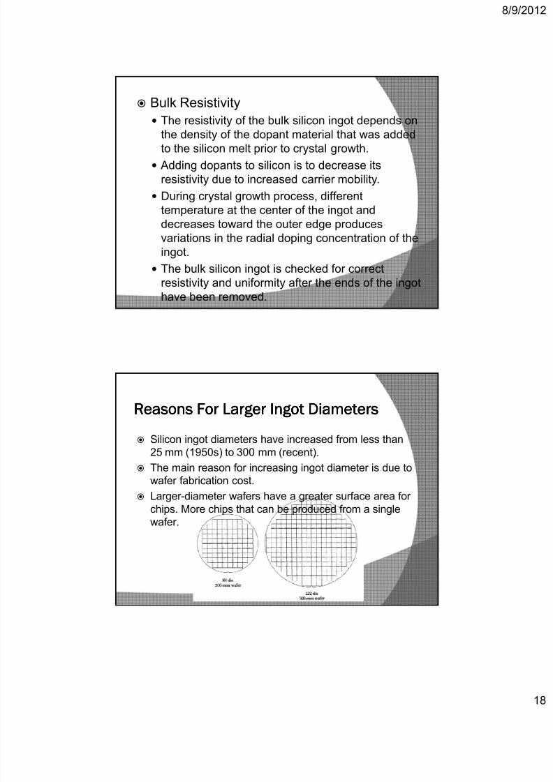
7212019 EE503 Topic 2 Hoo
httpslidepdfcomreaderfullee503-topic-2-hoo 1822
89
Bulk Resistivity
The resistivity of the bulk silicon ingot depends on
the density of the dopant material that was addedto the silicon melt prior to crystal growth
Adding dopants to silicon is to decrease its
resistivity due to increased carrier mobility
During crystal growth process different
temperature at the center of the ingot and
decreases toward the outer edge produces
variations in the radial doping concentration of the
ingot
The bulk silicon ingot is checked for correctresistivity and uniformity after the ends of the ingot
have been removed
Reasons For Larger Ingot DiametersReasons For Larger Ingot DiametersReasons For Larger Ingot DiametersReasons For Larger Ingot Diameters
Silicon ingot diameters have increased from less than
25 mm (1950s) to 300 mm (recent)
The main reason for increasing ingot diameter is due to
wafer fabrication cost
Larger-diameter wafers have a greater surface area for
chips More chips that can be produced from a single
wafer
7212019 EE503 Topic 2 Hoo
httpslidepdfcomreaderfullee503-topic-2-hoo 1922
89
Larger wafers means more chips per wafer leading to
improved equipment productivity due to economies of
scale for less handling per chip and less processing
time per chip It is estimated that conversion to a 300-mm wafer diameter will reduce the fabrication cost per
chip by approximately 30 through equipment
utilization improvements
Another benefit from larger-diameter wafers is that fewer
chips are near the edge of the wafer which translates
into higher production yield
Ultimately cost savings will be the major factor that
drives the industry toward a larger wafer diameter
Sources of Contamination
Seven sources of contamination in a wafer
fabrication facility are
1 Air
2 Humans
3 Facility
4 Water
5 Process chemicals
6 Process gases
7 Production equipment
7212019 EE503 Topic 2 Hoo
httpslidepdfcomreaderfullee503-topic-2-hoo 2022
89
1 Air
The most fundamental concept of a cleanroom is the
control of particles in the wafer fab air small airborne aerosol particles float and remain in the
air depositing on wafers as contamination and
creating killer defects
2 Humans
People are the greatest sources of contamination in a
cleanroom
Particles come from hair clothes dead skin
excessive movements talking coughing and
sneezing are damaging to semiconductors
Average person sheds over 10000000 particles perminute of 03 microm size and larger
Require cleanroom garment
3 Facility3 Facility3 Facility3 Facility
A simplified diagram of the air handling system in a wafer
fab cleanroom
7212019 EE503 Topic 2 Hoo
httpslidepdfcomreaderfullee503-topic-2-hoo 2122
89
Air Filtering
Air enters the cleanroom through special particulate filters
in the ceiling and passes with laminar flow to the floorand into the recirculation air system to return back to the
air filtering system with makeup air An exhaust system
is used to remove undesirable heat and chemicals
Temperature and Humidity
temperature control in a class 1 at 03 microm cleanroom is
68 plusmn 05deg
Relative humidity (RH) 40 +-10 - important because
of its contribution toward corrosion
Electrostatic Discharge Static-dissipative cleanroom
materials ESD grounding Air ionization
3 Water To manufacture semiconductors a high quality
ultrapure deionized (DI) water (sometimes referred
to as UPW) is required primarily in the chemical
wafer cleaning solutions and as a postclean rinse
Free from Dissolved ions Organic materials
Particulates Bacteria Silica and Dissolved oxygen
4 Process Chemicals Process Gases
Liquid chemicals used in semiconductor processing
must be free of contamination for successful device
yield and performance Filters are used to prevent chemical degradation
during delivery or to maintain chemical purity
during a recirculation step
Gases pass through purifiers and gas filters to
remove impurities and particles
7212019 EE503 Topic 2 Hoo
httpslidepdfcomreaderfullee503-topic-2-hoo 2222
89
5 Production Equipment Many wafer fabrication operations occur in a
vacuum which requires special design
considerations to avoid contamination
Since equipment automation means fewer
humans interacting with the product there is
less concern about particles from humans and
more emphasis on reducing particles from
equipment
CleanroomCleanroomCleanroomCleanroom The class number designates the air quality inside a
cleanroom by defining the particle size and density in
the cleanroom air
US Federal Standard 209E Examples
Class 10 at 02 microm - a maximum of 75 particles per
cubic foot at 02 microm or larger
Class 10 at 01 microm - a maximum of 350 particles per
cubic foot at 01 microm or larger
7212019 EE503 Topic 2 Hoo
httpslidepdfcomreaderfullee503-topic-2-hoo 1922
89
Larger wafers means more chips per wafer leading to
improved equipment productivity due to economies of
scale for less handling per chip and less processing
time per chip It is estimated that conversion to a 300-mm wafer diameter will reduce the fabrication cost per
chip by approximately 30 through equipment
utilization improvements
Another benefit from larger-diameter wafers is that fewer
chips are near the edge of the wafer which translates
into higher production yield
Ultimately cost savings will be the major factor that
drives the industry toward a larger wafer diameter
Sources of Contamination
Seven sources of contamination in a wafer
fabrication facility are
1 Air
2 Humans
3 Facility
4 Water
5 Process chemicals
6 Process gases
7 Production equipment
7212019 EE503 Topic 2 Hoo
httpslidepdfcomreaderfullee503-topic-2-hoo 2022
89
1 Air
The most fundamental concept of a cleanroom is the
control of particles in the wafer fab air small airborne aerosol particles float and remain in the
air depositing on wafers as contamination and
creating killer defects
2 Humans
People are the greatest sources of contamination in a
cleanroom
Particles come from hair clothes dead skin
excessive movements talking coughing and
sneezing are damaging to semiconductors
Average person sheds over 10000000 particles perminute of 03 microm size and larger
Require cleanroom garment
3 Facility3 Facility3 Facility3 Facility
A simplified diagram of the air handling system in a wafer
fab cleanroom
7212019 EE503 Topic 2 Hoo
httpslidepdfcomreaderfullee503-topic-2-hoo 2122
89
Air Filtering
Air enters the cleanroom through special particulate filters
in the ceiling and passes with laminar flow to the floorand into the recirculation air system to return back to the
air filtering system with makeup air An exhaust system
is used to remove undesirable heat and chemicals
Temperature and Humidity
temperature control in a class 1 at 03 microm cleanroom is
68 plusmn 05deg
Relative humidity (RH) 40 +-10 - important because
of its contribution toward corrosion
Electrostatic Discharge Static-dissipative cleanroom
materials ESD grounding Air ionization
3 Water To manufacture semiconductors a high quality
ultrapure deionized (DI) water (sometimes referred
to as UPW) is required primarily in the chemical
wafer cleaning solutions and as a postclean rinse
Free from Dissolved ions Organic materials
Particulates Bacteria Silica and Dissolved oxygen
4 Process Chemicals Process Gases
Liquid chemicals used in semiconductor processing
must be free of contamination for successful device
yield and performance Filters are used to prevent chemical degradation
during delivery or to maintain chemical purity
during a recirculation step
Gases pass through purifiers and gas filters to
remove impurities and particles
7212019 EE503 Topic 2 Hoo
httpslidepdfcomreaderfullee503-topic-2-hoo 2222
89
5 Production Equipment Many wafer fabrication operations occur in a
vacuum which requires special design
considerations to avoid contamination
Since equipment automation means fewer
humans interacting with the product there is
less concern about particles from humans and
more emphasis on reducing particles from
equipment
CleanroomCleanroomCleanroomCleanroom The class number designates the air quality inside a
cleanroom by defining the particle size and density in
the cleanroom air
US Federal Standard 209E Examples
Class 10 at 02 microm - a maximum of 75 particles per
cubic foot at 02 microm or larger
Class 10 at 01 microm - a maximum of 350 particles per
cubic foot at 01 microm or larger
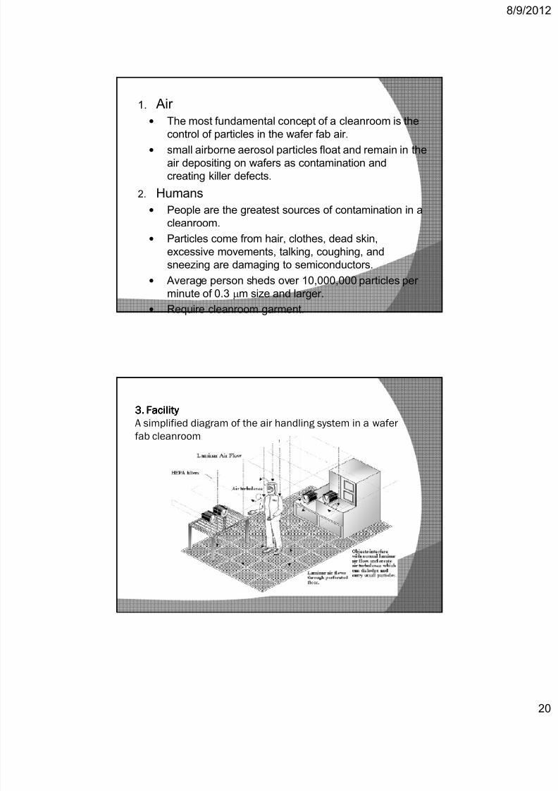
7212019 EE503 Topic 2 Hoo
httpslidepdfcomreaderfullee503-topic-2-hoo 2222
89
5 Production Equipment Many wafer fabrication operations occur in a
vacuum which requires special design
considerations to avoid contamination
Since equipment automation means fewer
humans interacting with the product there is
less concern about particles from humans and
more emphasis on reducing particles from
equipment
CleanroomCleanroomCleanroomCleanroom The class number designates the air quality inside a
cleanroom by defining the particle size and density in
the cleanroom air
US Federal Standard 209E Examples
Class 10 at 02 microm - a maximum of 75 particles per
cubic foot at 02 microm or larger
Class 10 at 01 microm - a maximum of 350 particles per
cubic foot at 01 microm or larger