effect of gallium incorporation on the properties of zno
TRANSCRIPT

Effect of Gallium incorporation on the properties of ZnO thin films
S. Kurtaran*, S. Aldağ, G. Öföfoğlu
Eskişehir Osmangazi Universitesi, Fizik Bölümü, 26480 Eskisehir, Türkiye
Abstract
Ga doped ZnO thin films were formed by the Ultrasonic Chemical Spray Pyrolysis method
onto substrates using zinc acetate and gallium (III) nitrate hydrate as precursors. The
structural, optical, surface and electrical properties were studied as a function of increasing Ga
doping concentration from 0 to 6 at %. Structural studies were shown polycrystalline with a
hexagonal crystal structure. The transparency in the visible range was around 85% for thin
film deposited using 6 at % Ga doping. With the aim of determining surface images and
surface roughness of the films atomic force microscope images were taken. Ga doping of ZnO
thin films could markedly decrease surface roughness. Electrical resistivity was determined
by four point method. The resistivity 2.0% Ga doped ZnO film was the lowest resistivity of
1.7 cm. In the photoluminescence measurements of the films, existence of UV and defect
emission band was observed. As a result, Ga doped ZnO films have advanced properties and
promising materials for solar cells.
Keywords: Ga-doped ZnO; chemical spray technique; XRD; AFM; Optical properties;
Electrical properties.
1. Introduction
Transparent conductive oxide (TCO) thin films have a very important place in
optoelectronic applications. The most developed TCO tecnology for practical applications is
based on indium tin oxide (ITO) [1]. Recently, zinc oxide (ZnO) has emerged as an important
transparent conductive metal oxide capable of replacing commonly used expensive ITOs.
ZnO is a transparent semiconductor material composed of lI-VI type with natural n-type
conductivity. ZnO is a non-toxic material found abundantly in nature. It has also emerged as
one of the most promising materials due to its optical and electrical properties. [2]. Group III
Preprints (www.preprints.org) | NOT PEER-REVIEWED | Posted: 14 January 2019
© 2019 by the author(s). Distributed under a Creative Commons CC BY license.
Preprints (www.preprints.org) | NOT PEER-REVIEWED | Posted: 14 January 2019 doi:10.20944/preprints201901.0138.v1
© 2019 by the author(s). Distributed under a Creative Commons CC BY license.

A elements Al, In, Ga and B have been frequently used as n type dopants for ZnO [3]. Ga-
doped ZnO (GZO) has also drawn attraction in the recent times as well as doping-free ZnO
[4-7]. Because oxidation of GZO is more stable due to high electro-negativity of gallium [8].
GZO with low electrical resistance and high optical transparency in visible region is one of
the most suitable candidates for alternative TCO films. [9]. In order to obtain Ga-doped ZnO
films, various thin-film production techniques such as magnetron spraying [10-13], chemical
spray pyrolysis[14-21], sol-gel [22-24], chemical steam deposition (MOCVD) [25,26],
pulsed laser deposition (PLD) [27-29] and ion plating with DC arc discharge [30,31] are used.
The chemical spray technique among these techniques is widely used thanks to its advantages
in terms of that the films produced have wide surfaces as well as that it is economic and
simple. In this paper, undoped and Ga-doped (2,4 and 6%) ZnO films were produced by
using Ultrasonic Chemical Spray technique (USP) and their electrical, optical, structural and
surface properties were researched.
2. Experimental Details
USP technique of salts of solid samples and inorganic compounds by mixing the
solution at the desired volume prepared in specific concentrations allow the production of thin
films and then they are spraying the preheated glass substrate. [32]. The films were produced
on glass substrates with USP technique. Zn(CH3COO)2·2H2O was used as Zn source and
Gallium (III) nitrate hydrate [Ga(NO3)3·xH2O] was used as Ga source in order to obtain the
films. The production parameters and codes of the films are given in Table 1. The solution
was sprayed on preheated onto glass substrates at 5 ml/min. Flow rate controlled using flow
meter. In order to examine the structural properties of the films, XRD patterns were taken at
302θ70 by “Rigaku X-Ray Diffractometer” with the powder method by using CuKα
radiation (λ=1.5406 Ǻ). With the "Park Systems XE 100 model", the surface properties of the
films were taken. Also, rms (Rq) and average (Ra) roughness values were determined.
Thicknesses of the films (t), values, refractive indexes (n) and extinction coefficients (k)
were determined by “OPT-S9000 Spectroscopic Elipsometer (SE)” with 250-2300 nm
measuring range. Transmittance (T) spectra were taken by “Shimadzu-2550 UV-Vis
Spectrophotometer’’ with 300-900 nm measuring range. Also, optical band gaps (Eg) of all
films were determined by the optical method. “Keithley 2601A LUCAS Labs PRO4” device
was used to determine the electrical resistivity of the films. Also, photoluminescence spectra
(PL) of the films were taken by “Perkin Elmer LS55 Fluorescence Spectrometer”.
Preprints (www.preprints.org) | NOT PEER-REVIEWED | Posted: 14 January 2019 Preprints (www.preprints.org) | NOT PEER-REVIEWED | Posted: 14 January 2019 doi:10.20944/preprints201901.0138.v1

Table 1. Codes and production parameters of GZO.
3. Results and Discussions
3.1. Structural properties
Figure 1 shows the XRD patterns of the films the existence of a strong peak
corresponding to (0 0 2) and weak peaks corresponding to (1 0 1), (1 0 2) and (1 0 3) of the
wurtzite phase of ZnO. Existence of peaks having different intensity and widths is an
indicator of that the films form at a polycrystalline structure [33]. As the amount of Ga in the
film increases, the density of the peaks decreases. This behaviour indicates that deteriorates
the crystallinity of the films. This is due to the stresses caused by the difference in the ionic
radii of zinc and gallium. In Table 2, it draws attraction that 2 and d values belonging to the
films show difference in accordance with the values given in JCPDS (00-036-1451) [34]. In
Table 2, it is seen that (0 0 2) refraction peak in the films peak shifted towards higher angles
compared to Z0 peak. This case indicates that Ga+3 (0.62Å) having a small ionic radius took
the place of Zn+2 (0.74 Å) ion having a bigger ionic radius [35]. Grain size (D) values can be
calculated using the Debye-Scherrer formula given below;
CosBD
94.0=
(1)
Film Kod Molarite Püskürtme Süresi Taban Sıcaklığı
ZnO Z0 0.1 M 20dk 350±5 C
ZnO:Ga %2 GZO-2 0.1 M 20dk 350±5 C
ZnO:Ga %4 GZO-4 0.1 M 20dk 350±5 C
ZnO:Ga %6 GZO-6 0.1 M 20dk 350±5 C
Preprints (www.preprints.org) | NOT PEER-REVIEWED | Posted: 14 January 2019 Preprints (www.preprints.org) | NOT PEER-REVIEWED | Posted: 14 January 2019 doi:10.20944/preprints201901.0138.v1

where is the x-ray wavelength used, β is the full-width at half maximum (FWHM) of the
diffraction peak and is the Bragg’s angle [36, 37]. Table 2 shows that disrupt the
crystallinity of the contribution from Ga.
Preprints (www.preprints.org) | NOT PEER-REVIEWED | Posted: 14 January 2019 Preprints (www.preprints.org) | NOT PEER-REVIEWED | Posted: 14 January 2019 doi:10.20944/preprints201901.0138.v1

Preprints (www.preprints.org) | NOT PEER-REVIEWED | Posted: 14 January 2019 Preprints (www.preprints.org) | NOT PEER-REVIEWED | Posted: 14 January 2019 doi:10.20944/preprints201901.0138.v1

Fig 1.
Table 2. The data and structural parameters belonging to XRD patterns of GZO films.
3.2. Optical properties
The thicknesses and optical constants of the films are determined by SE. The
polarization state of the electromagnetic wave is given by and , which are known as
ellipsometric parameters. Thus, information about the sample that changes the polarization
state is obtained. and parameters are measured as wavelength function in SE
measurements [38]. Elipsometric data analysis requires an optical model that defines the layer
thickness and optical constants of the sample. The Cauchy model is suitable for areas where
the extinction coefficient is zero. The Urbach equation represents the extinction coefficient of
the region where the material has little absorption [39]. Cauchy-Urbach model is used for
fitting the experimental data. SE measurements have been taken at a wavelength range of
1200-1600 nm. In order to determine the thickness of all films with high precision, polarized
light are sent at different angles (60°, 65°, 70°) on the material, and spectra are taken. The
best angle for spectra was determined as 70°. Figure 2 are showed spectra of the films.
Film 2 () d (Ǻ) 20 ()
(ASTM)
d0 (Ǻ)
(ASTM) (hkl) D (nm)
Z0 34.22 2.618 34.42 2.603 (002) 35
36.06 2.489 36.25 2.476 (101) 30
GZO-2 34.48 2.599 34.42 2.603 (002) 29
36.42 2.477 36.25 2.476 (101) 24
GZO-4 34.40 2.605 34.42 2.603 (002) 18
36.20 2.479 36.25 2.476 (101) 18
GZO-6 34.54 2.595 34.42 2.603 (002) 26
36.36 2.469 36.25 2.476 (101) 26
Preprints (www.preprints.org) | NOT PEER-REVIEWED | Posted: 14 January 2019 Preprints (www.preprints.org) | NOT PEER-REVIEWED | Posted: 14 January 2019 doi:10.20944/preprints201901.0138.v1

The coherence between theoretical model and experimental data is good. But in the films, it
draws attraction that there are deviations at experimental and theoretical values. Such a
deviation may have been occurred due to the data taken in spectroscopic elipsometer
technique which is sensitive to surfaces of the films. Another reason of the deviation may
have been the grain boundaries. It is previously seen that there is a decrease at crystallization
level with addition of Ga element. Thicknesses (t) and modeling parameters of all films are
given in Table 3. It is noteworthy that the thickness values decrease with Ga incorporation.
Fig 2.
Table 3. Cauchy-Urbach model parameters, thickness values and optical constants of GZO
films.
Film t (nm) An Bn (nm)2 Cn (nm)4 Ak Bk (eV)-1 n k
Z0 135 1.914 0.0100 0.011 0.29 1.09 1.922 0.0233
Preprints (www.preprints.org) | NOT PEER-REVIEWED | Posted: 14 January 2019 Preprints (www.preprints.org) | NOT PEER-REVIEWED | Posted: 14 January 2019 doi:10.20944/preprints201901.0138.v1

Figure 3 are showed transmittance spectra of the films. When the films are looked to
naked eye, they are transparent and homogenous [40]. This has been also validated with
transmittance spectrums. The transmittance in the visible area is approximately %80. An
increase is also discusses at average transmittance values in visible area of the films with Ga
doping. It is good for device application that the transmittance of the doped films are
increased in the visible area.
Fig 3.
GZO-2 39 2.201 0.0106 0.0014 0.35 1.386 2.206 0.0135
GZO-4 59 2.079 0.0102 0.0015 0.36 1.386 2.085 0.0136
GZO-6 51 2.031 0.0100 0.002 0.36 1.385 2.037 0.0139
Preprints (www.preprints.org) | NOT PEER-REVIEWED | Posted: 14 January 2019 Preprints (www.preprints.org) | NOT PEER-REVIEWED | Posted: 14 January 2019 doi:10.20944/preprints201901.0138.v1

(αhν)2h graphs of the films are in Figure 4. Optical band gap values of the films have
been determined by optical method [41]. Optical band gap values of the films Z0, GZO-2,
GZO-4 and GZO-6 have been calculated to be 3.27, 3.28, 3.28 and 3.28 eV, respectively. All
films have direct band gap transitions.
Fig 4.
PL spectroscopy is an important tool to characterize defects in semiconductors [42].
PL spectrums of the films taken with 3.82 eV excitation energy at room temperature are given
in Figure 5. When PL spectrums are examined, it is determined that UV emission are at
390 nm (3.18 eV) (1th peak); blue emission is at 440 nm (2.76 eV) (2nd peak); green
emission is at 490 nm (2.5 eV) (3rd peak); yellow-orange emission is at 550 nm (2.25 eV)
(4th peak) and orange emission is at 590 nm (2.11 eV) (5th peak) [43,44]. The intensity of 1th
Preprints (www.preprints.org) | NOT PEER-REVIEWED | Posted: 14 January 2019 Preprints (www.preprints.org) | NOT PEER-REVIEWED | Posted: 14 January 2019 doi:10.20944/preprints201901.0138.v1

peak defined as UV emission peak decreased with the increase of Ga amount in GZO-4 and
GZO-6 films compared to Z0 film. The intensity of 2nd peak increased in GZO-2 film
compared to others. We may say that this case was resulted from the interstitial zinc (Zni) [19,
20]. We think that weakening of this peak in GZO-4 and GZO-6 films are resulted from the
changes on distributions of Zni atoms in the optical band gap along with Ga doping. 3rd peak
corresponding to the green emission in PL spectra is an indicator for existence of oxygen
vacancies (Vo) that act as a deep visible trap in the structure [40]. The increase in the intensity
of this peak draws attraction especially in GZO-2 films. 4th and 5th peaks that show yellow-
orange and orange emissions are indicators of intersitial oxygen (Oi). Increase of peak
intensity representing the orange emission in the films brings the idea of increase of density of
the oxygen vacancies to the mind. This case is clearly seen in GZO-2 film. In GZO-4 and
GZO-6 films, it may be said that interstitial oxygen had decreased.
Fig 5.
Preprints (www.preprints.org) | NOT PEER-REVIEWED | Posted: 14 January 2019 Preprints (www.preprints.org) | NOT PEER-REVIEWED | Posted: 14 January 2019 doi:10.20944/preprints201901.0138.v1
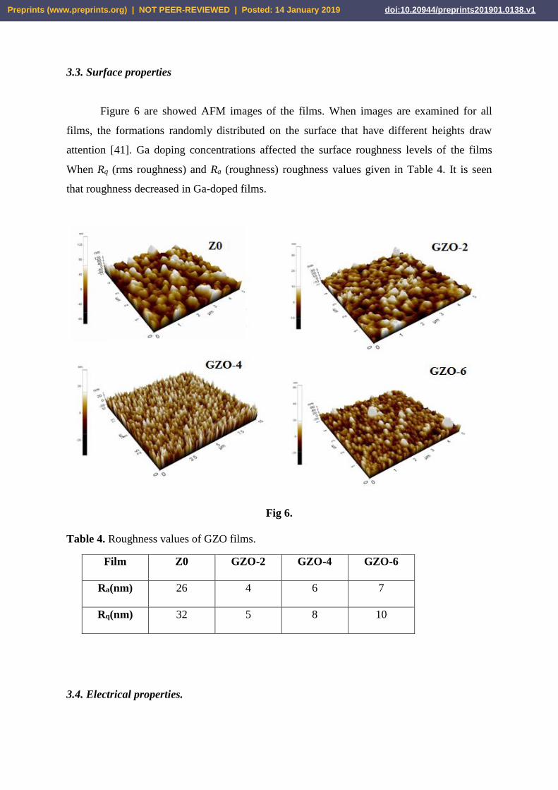
3.3. Surface properties
Figure 6 are showed AFM images of the films. When images are examined for all
films, the formations randomly distributed on the surface that have different heights draw
attention [41]. Ga doping concentrations affected the surface roughness levels of the films
When Rq (rms roughness) and Ra (roughness) roughness values given in Table 4. It is seen
that roughness decreased in Ga-doped films.
Fig 6.
Table 4. Roughness values of GZO films.
3.4. Electrical properties.
Film Z0 GZO-2 GZO-4 GZO-6
Ra(nm) 26 4 6 7
Rq(nm) 32 5 8 10
Preprints (www.preprints.org) | NOT PEER-REVIEWED | Posted: 14 January 2019 Preprints (www.preprints.org) | NOT PEER-REVIEWED | Posted: 14 January 2019 doi:10.20944/preprints201901.0138.v1

Resistivity values of the films ZO, GZO-2, GZO-4 and GZO-6 have been
determined to be 29.4, 1.7, 1.9 and 3.0 Ωcm, respectively. The resistivity of the Z0 is higher
than that of the Ga doped films. We think that this case is related to additional electron as a
result of replacement of Ga+3 ion entering into the structure with Zn+2 ion. Also, the defects
such as interstitial Ga+3 or interstitial zinc (Zni) or oxygen vacancies(V0) as well as Ga doping
may take a role in the increase of carrier densities by playing a role in this case [46].
4. Conclusions
Ga doped ZnO films have been deposited onto glass substrates by USP technique. The Ga
element doping procedure has been selected at three different rates of 2%, 4% and 6%.
Structural, optical, surface and electrical properties of the films have been researched. XRD
patterns of the films have a polycrystalline structure. x-ray diffraction studies have shown that
the level of crystallinity is impaired by the effect of the element Ga. That is, successfully
substitution of Ga+3 ions with Zn+2 ions has been applied. Spectroscopic ellipsometry
technique is used to determine the thicknesses and optical constants of the films. It is seen that
the optical permeability of the films is the contribution of gallium. It appears that Ga does not
have an effect on the optical band gap values. The minumum resistivity achieved for Ga
doped ZnO thin films. As a result of reviewing optical, structural, surface and electrical
properties of all films obtained, it was determined that amount of the doping element
significantly affected physical properties of ZnO films. It was also concluded that the films
may be used in solar cells as transparent front contact due to their opto-electronic properties.
Acknowledgments
Acknowledgments This study was by supported Eskisehir Osmangazi University BAP
Commission (Grant No: 201219022).
References
Preprints (www.preprints.org) | NOT PEER-REVIEWED | Posted: 14 January 2019 Preprints (www.preprints.org) | NOT PEER-REVIEWED | Posted: 14 January 2019 doi:10.20944/preprints201901.0138.v1
[1] T. Terasako, Y. Ogura, S. Fujimoto, H. Song, H. Makino, M. Yagi, S. Shirakata, T.
Yamamoto, 2013, Carrier transport and photoluminescence properties of Ga-doped ZnO films
grown by ion-plating and by atmospheric-pressure CVD, Thin Solid Films 549, 12-17.
[2] Taewook Nam, Chang Wan Lee, Hyun Jae Kim, Hyungjun Kim, Growth characteristics
and properties of Ga-doped ZnO (GZO) thin films grown by thermal and plasma-enhanced
atomic layer deposition, Applied Surface Science 295 (2014) 260– 265.
[3] I.A. Buyanova, X.J. Wang, W.M. Wang, C.W. Tu, W.M. Chen, Effects of Ga doping on
optical and structural properties of ZnO epilayers, Superlattices and Microstructures 45
(2009) 413-420.
[4] S. Shionoya and W. H. Yen (ed), 1997, Phosphor Handbook By Phosphor Research
Society Chapter 2 Zinc Oxide (Boca Raton, FL: CRC Press).
[5] X. Bie, J.G.Lu, L. Gong, L. Lin, B.H. Zhao, Z.Z.Ye, 2009, Transparent conductive
ZnO:Ga films prepared by DC reactive magnetron sputtering at low temperature
Appl.Surf.Sci.256, 289–293.
[6] Kyung-Jun Ahn, Sanghun Lee, Won-Jeong Kim, GeunYoungYeom, Woong Lee, 2013
Characteristics of Ga-doped ZnO films deposited by pulsed DC magnetron sputtering at low
temperature Materials ScienceinSemiconductorProcessing 16, 1957–1963.
[7] Reza Ebrahimifard, Mohammad Reza Golobostanfard, Hossein Abdizadeh, 2014, Sol–gel
derived Al and Ga co-doped ZnO thin films: An optoelectronic study Applied Surface Science
290, 252– 259.
[8] H. Mahdhi, Z. Ben Ayadi, S. Alaya, J.L. Gauffier, K. Djessas, 2014, The effects of dopant
concentration and deposition temperature on the structural, optical and electrical properties of
Ga-doped ZnO thin films, Superlattices and Microstructures 72, 60–71.
[9] M. Gabás, E. Ochoa-Martínez, E. Navarrete-Astorga, A.R. Landa-Cánovas, P. Herrero, F.
Agulló-Rueda, S. Palanco, J.J. Martínez-Serrano, J.R. Ramos-BarradoCharacterization of the
Preprints (www.preprints.org) | NOT PEER-REVIEWED | Posted: 14 January 2019 Preprints (www.preprints.org) | NOT PEER-REVIEWED | Posted: 14 January 2019 doi:10.20944/preprints201901.0138.v1

interface between highly conductive Ga:ZnO films and the silicon substrate Applied Surface
Science 419 (2017) 595–602.
[10] K. Yim, H.W. Kim, C. Lee, 2007, Effects of annealing on structure, resistivity and
transmittance of Ga doped ZnO films Mater. Sci. Technol. 23, 108–112.
[11] X. Bie, J.G. Lu, L. Gong, L. Lin, B.H. Zhao, Z.Z. Ye, 2009, Transparent conductive
ZnO:Ga films prepared by DC reactive magnetron sputtering at low temperature
Appl.Surf.Sci. 256, 289–293.
[12] Yutaka Kishimoto, Osamu Nakagawara, Hiroyuki Seto, Yoshihiro Koshido, Yukio
Yoshino, 2009, Improvement in moisture durability of ZnO transparent conductive films with
Ga heavy doping process, Vacuum 83, 544–547.
[13] E. Fortunato, V. Assuncao, A. Goncalves, A. Marques, H. Aguas, L. Pereira, I. Ferreira,
P. Vilarinho, R. Martins, 2004, High quality conductive gallium-doped zinc oxide films
deposited at room temperature Thin Solid Films, 443–447.
[14] A.R Babar, P.R Deshamukh, R.J. Deokate, D. Haranath, C.H. Bhosale and K.Y.
Rajpure, 2008, Gallium doping in transparent conductive ZnO thin films prepared by
chemical spray pyrolysis, J. Phys. D: Appl. Phys. 41, 135404.
[15] G.G. Untila, T.N. Kost, A.B. Chebotareva, D.A. Zuev, A.S. Stepanov, 2015, Pyrosol-
deposited Ga-doped ZnO (GZO) transparent electrodes inGZO/(p+nn+)c-Si solar cells
Vacuum 114, 188-197.
[16] H. Gomez, M. de la L. Olvera, 2006, Ga-doped ZnO thin films: Effect of deposition
temperature, dopant concentration, and vacuum-thermal treatment on the electrical, optical,
structural and morphological properties Materials Science and Engineering B 134, 20–26.
Preprints (www.preprints.org) | NOT PEER-REVIEWED | Posted: 14 January 2019 Preprints (www.preprints.org) | NOT PEER-REVIEWED | Posted: 14 January 2019 doi:10.20944/preprints201901.0138.v1

[17] H. Gomez, A. Maldonado, M. de la L. Olvera, D.R. Acosta, 2005, Gallium-doped ZnO
thin films deposited by chemical spray, Solar Energy Materials & Solar Cells 87, 107–116.
[18] Minoru Oshima, Akiko Ide, Akiko Mochihara, Kenji Yoshino, Yujin Tanikemoto, Kouji
Toyota, Koichiro Inaba, Ken-ichi Haga, Toshio Naka, and Koichi Tokudome, 2013, Optical
and electrical characterization of transparent Ga-doped ZnO thin films grown by atmospheric
spray pyrolysis using diethylzinc solution, Phys. Status Solidi C 10, No. 7–8, 1015–1018.
[19] T. Prasada Rao, M.C. Santhosh Kumar, 2010, Physical properties of Ga-doped ZnO thin
films by spray pyrolysis, Journal of Alloys and Compounds 506, 788–793.
[20] S.S. Shinde, P.S. Shinde, Y.W. Oh, D. Haranath, C.H. Bhosale, K.Y. Rajpure, 2012,
Structural, optoelectronic, luminescence and thermal properties of Ga-doped zinc oxide thin
films, Applied Surface Science 258, 9969– 9976.
[21] A.Amala Rani, Suhashini Ernest, 2014, Structural, morphological, optical and
compositional characterization of spray deposited Ga doped ZnO thin film for Dye-Sensitized
Solar Cell application, Superlattices and Microstructures 75, 398–408.
[22] Russell Binions, Shuqun Chen, Michael E.A.Warwick, Russell Binions, 2015, Effects of
film thickness and thermal treatment on the structural and opto-electronic properties of Ga-
doped ZnO films deposited by sol–gel method, Solar Energy Materials & Solar Cells 137,
202–209.
[23] I. Ghiloufi, J.El Ghoul, A.Modwi a, L.El Mir, 2016, Ga-doped ZnO for adsorption of
heavy metals from aqueous solution, Materials Science in Semiconductor Processing42, 102–
106.
[24] M. Hjiri, R. Dhahri, L. El Mira, A. Bonavita, N. Donato, S.G. Leonardi, G. Neri, 2015
CO sensing properties of Ga-doped ZnO prepared by sol–gel route, Journal of Alloys and
Compounds, 187–192
Preprints (www.preprints.org) | NOT PEER-REVIEWED | Posted: 14 January 2019 Preprints (www.preprints.org) | NOT PEER-REVIEWED | Posted: 14 January 2019 doi:10.20944/preprints201901.0138.v1

[25] J.H. Liang, K.T. Chou, Y.J. Chen, C.Z. Yang, Growth of Ga-doped ZnO thin film
prepared by MOCVD for TCO application,
[26] G.A. Hirata, J. McKittrick, T. Cheeks, J.M. Siqueiros, J.A. Diaz, O. Contreras, O.A.
Lopez, Synthesis and optelectronic characterization of gallium doped zinc oxide transparent
electrodes, Thin Solid Films 288 (1996) 29-31.
[27] J.A. Sans, J.F. Sanchez-Royo, A. Segura, 2008, Study of the bandgap renormalization in
Ga-doped ZnO films by means of optical absorption under high pressure and photoelectron
spectroscopy, Superlattices and Microstructures 43, 362–367
[28] Sang-Moo Park, Tomoaki Ikegami, Kenji Ebihara, 2006, Effects of substrate temperature
on the properties of Ga-doped ZnO by pulsed laser deposition, Thin Solid Films 513, 90–94.
[29] Hisao Makino, Huaping Song, Tetsuya Yamamoto, 2014 Influences of oxygen gas flow
rate on electrical properties of Ga-doped ZnO thin films deposited on glass and sapphire
substrates, Thin Solid Films 559, 78–82.
[30] Yasushi Sato, Hisao Makino, Naoki Yamamoto, Tetsuya Yamamoto, 2011 Structural,
electrical and moisture resistance properties of Ga-doped ZnO films, Thin Solid Films 520,
1395–1399.
[31] K. Iwata, T. Sakemi, A. Yamada, P. Fons, K. Awai, T. Yamamoto, M. Matsubara, H.
Tampo,S. Niki, 2003, Growth and electrical properties of ZnO thin films deposited by novel
ion plating method, Thin Solid Films 445, 274–277.
[32] F. Atay, S. Kose, V. Bilgin, I. Akyuz, 2003, CdS:Ni films obtained by ultrasonic spray
pyrolysis: effect of the Ni concentration Materials Letters 57 (2003) 3461-3472.
[33] S. Benramache, F. Chabane, B. Benhaoua, Influence of growth time on crystalline
structure, conductivity and optical properties of ZnO thin films, J. Semicond. 34 (2013)
(023001-1).
Preprints (www.preprints.org) | NOT PEER-REVIEWED | Posted: 14 January 2019 Preprints (www.preprints.org) | NOT PEER-REVIEWED | Posted: 14 January 2019 doi:10.20944/preprints201901.0138.v1

[34] Charles Moditswe, Cosmas M. Muiva, Albert Juma Highly conductive and transparent
Ga-doped ZnO thin films deposited by chemical spray pyrolysis, Optik 127 (2016) 8317–
8325
[35] S. Kuo, W. Chen, F. Lai, C.Cheng, H. Kuo, S.Wang, W. Hsieh, 2006, Effects of doping
concentration and annealing temperature on properties of highly-oriented Al doped ZnO
films, J. Cryst. Growth., 287,78–84
[36] Benramdane, N., Murad, W.A., Misho, R.H., Ziane, M. and Kebbab, Z., 1997, A
chemical method for the preparation of thin films of CdO and ZnO, Materials Chemistry and
Physics, 48, 119-123.
[37] Cullity, B., Structure of polycrystalline aggregates. Elements of X-ray Diffraction,
(1978), p. 284.
[38] Hiroyuki Fujiwara and Michio Kondo, Effects of carrier concentration on the dielectric
function of ZnO:Ga and In2O3:Sn studied by spectroscopic ellipsometry: Analysis of free-
carrier and band-edge absorption, Physical Review B 71, 075109 (2005) 1-10.
[39] J.M. Khoshman, M.E. Kordesch, Spectroscopic ellipsometry characterization of
amorphous aluminum nitride and indium nitride thin films, Phys. Status Solidi (C) 2 (2005)
2821-2827.
[40] A. R. Babar, P. R. Deshamukh, R. J. Deokate, D. Haranath, C. H. Bhosale and K. Y.
Rajpure, Gallium doping in transparent conductive ZnO thin films prepared by chemical
spray pyrolysis, J. Phys. D: Appl. Phys. 41 (2008) 135404 1-6.
[41] Chien-Yie Tsay, Chun-Wei Wu, Chien-Ming Lei, Fan-Shiong Chen, Chung-Kwei Lin,
Microstructural and optical properties of Ga-doped ZnO semiconductor thin films prepared by
sol–gel process, Thin Solid Films 519 (2010) 1516–1520.
[42] Hafdallah A, Yanineb F, Aida M S, et al., 2011, In doped ZnO thin films. Journal of
Alloys and Compounds, 509(18), 7267.
Preprints (www.preprints.org) | NOT PEER-REVIEWED | Posted: 14 January 2019 Preprints (www.preprints.org) | NOT PEER-REVIEWED | Posted: 14 January 2019 doi:10.20944/preprints201901.0138.v1

[43] D.-T. Phan, A.A.M. Farag, F. Yakuphanoğlu, G.S. Chung, 2012, Optical and
photoluminescence properties of Ga doped ZnO nanostructures by sol-gel method,
J.Electroceram 29, 12-22.
[44] Pradipta K Nayak, Jihoon Yang, Jinwoo Kim, Seungjun Chung, Jaewook Jeong,
Changhee Lee and Yongtaek Hong, Spin-coated Ga-doped ZnO transparent conducting thin
films for organic light-emitting diodes, J. Phys. D: Appl. Phys. 42 (2009) 035102,1-6.
[45] J.L. Zhao, X.W. Sun, H. Ryu, Y.B. Moon, 2011, Thermally stable transparent conducting
and highly infrared reflective Ga-doped ZnO thin films by metal organic chemical vapor
deposition, Optical Materials 33, 768–772.
[46] Zhang D H, Yang T L, Ma J, et al., 2000, Preparation of transparent conducting ZnO:Al
films on polymersubstrates by r. f. Magnetron sputtering. Appl Surf Sci, 158(1): 43
FIGURE CAPTIONS
Fig. 1. XRD patterns of GZO films.
Fig. 2. spectrums of GZO films.
Fig. 3. Transmittance spectra of GZO films.
Fig. 4. (αh)2h alteration graphics of GZO films.
Preprints (www.preprints.org) | NOT PEER-REVIEWED | Posted: 14 January 2019 Preprints (www.preprints.org) | NOT PEER-REVIEWED | Posted: 14 January 2019 doi:10.20944/preprints201901.0138.v1

Fig. 5. PL spectra of GZO films
Fig. 6. AFM images of GZO films.
TABLE CAPTIONS
Table 1. Codes and production parameters of GZO films.
Table 2. The data and structural parameters belonging to XRD patterns of GZO films.
Table 3. Cauchy-Urbach model parameters, thickness values and optical constants of GZO
films.
Table 4. Roughness values of GZO films.
Preprints (www.preprints.org) | NOT PEER-REVIEWED | Posted: 14 January 2019 Preprints (www.preprints.org) | NOT PEER-REVIEWED | Posted: 14 January 2019 doi:10.20944/preprints201901.0138.v1