effect of nanosecond laser dicing on ultrathin...
TRANSCRIPT
EFFECT OF NANOSECOND LASER DICING ON
ULTRATHIN SILICON DIE WITH COPPER
STABILIZATION LAYER
MICHAEL RAJ MARKS
UNIVERSITI SAINS MALAYSIA
2016

EFFECT OF NANOSECOND LASER DICING ON
ULTRATHIN SILICON DIE WITH COPPER
STABILIZATION LAYER
by
MICHAEL RAJ MARKS
Thesis submitted in fulfillment of the
requirements for the degree
of Master of Science
August 2016
ii
ACKNOWLEDGEMENT
I would like to thank my main supervisor, Prof. Dr. Zainuriah Hassan, and
my co-supervisor, Prof. Ir. Dr. Cheong Kuan Yew for their invaluable guidance,
insightful discussions, and encouragement throughout the course of this research.
I would like to express my gratitude to Karl Mayer, Dr. Evelyn Napetschnig
and Dr. Wolfgang Diewald for their assistance in formulating and approving this
research project, for providing all the necessary resources within Infineon to support
the research, and for their genuine interest in my work.
My special thanks goes out to the following colleagues in Villach, Austria,
whom have spent a lot of their precious time in deep technical discussions with me
and inspired me with ideas on the ultrathin wafer fabrication techniques: Hermine
Winkler, Dr. Bernhard Goller, Thomas Hrast, Dr. Ulrike Fastner, Dr. Michael Fuchs,
Dr. Michael Ehmann, Dr. Petra Fischer, Paul Ganitzer, Rudolf Rothmaler, Thomas
Zell, Seebacher Gottfried, Dr. Carsten Koblinski, Robert Muhr and Dr. Michael
Pinczolits. I would also like to thank them for making me feel at home in Villach,
and enduring the six months away from my family in Malaysia. I would like to thank
the following colleagues in Kulim and Melaka for their assistance in the Failure
Analysis Lab: Cheong Cheok Fei, Chong May Wan, Dinah On, Chin Ee Mei, Yong
Foo Khong and Tan Pin Pin. A special thanks to Chin Che Woei for his assistance in
the NOR Lab, USM.
Last but not least, I would like to express my special gratitude to my wife
Julia, and to my sons, Gabriel and Benjamin, for their patience, unwavering support
and for their understanding during all the evenings and weekends when I had to
sacrifice my time with them.

iii
TABLE OF CONTENTS
ACKNOWLEDGEMENT ii
TABLE OF CONTENTS iii
LIST OF TABLES vii
LIST OF FIGURES viii
LIST OF SYMBOLS xvii
LIST OF ABBREVIATIONS xviii
ABSTRAK xx
ABSTRACT xxii
CHAPTER 1: INTRODUCTION 1
1.1 Introduction 1
1.2 Research objectives 4
1.3 Research originality 4
1.4 Scope of study 5
1.5 Organization of thesis 6
CHAPTER 2: LITERATURE REVIEW 8
2.1 Introduction 8
2.2 Wafer carrier systems 8
2.2.1 Carrier systems with temporary bonding/debonding
2.2.1(a) Wafer Support System (WSS)
8
12

iv
2.2.1(b) WaferBOND HT10.10
2.2.1(c) T-MAT
13
14
2.3 Wafer backgrinding 16
2.3.1 Types of backgrinding 16
2.3.2 Subsurface damage control 21
2.4 Wafer post-grinding treatment methods
2.4.1 Wet etching
24
24
2.5
2.6
Wafer dicing
2.5.1 Mechanical blade dicing
2.5.2 Ablative laser dicing
2.5.3 Plasma dicing
Summary
28
28
31
36
38
CHAPTER 3: MATERIALS AND INSTRUMENTS 40
3.1 Introduction 40
3.2 Glass carrier bonder 40
3.3 Wafer backgrinder 42
3.4 Spin-etch processor 44
3.5 Sputter coater 45
3.6 Electroplating 47
3.7
3.8
3.9
Glass carrier debonder
Laser dicing
Characterization instrumentation
3.9.1 Materialographic grinder/polisher
3.9.2 High-power optical microscope
49
51
52
52
54

v
3.9.3 Scanning electron microscope
3.9.4 Universal testing machine
3.9.5 Focused ion beam
3.9.6 Transmission electron microscope
55
57
59
61
3.10 Summary 64
CHAPTER 4: MATERIAL FABRICATION AND
CHARACTERIZATION PROCEDURES
65
4.1 Introduction 65
4.2 Ultrathin wafer and die fabrication 65
4.3 Laser dicing 69
4.4 Characterizations 71
4.4.1 Materialographic analysis 71
4.4.2 Mechanical strength analysis 72
4.4.3 Fractographic analysis 75
4.4.4 Die sidewall defect characterization 76
4.5 Summary 78
CHAPTER 5: RESULTS AND DISCUSSIONS 79
5.1 Introduction 79
5.2 General inspection of fabricated ultrathin dies 79
5.3 Materialographic cross-sectional analysis of ultrathin die 82
5.4 Mechanical strength testing 85
5.5 Stress analysis 89
5.6 Fractographic analysis 92
5.7 Die sidewall defect characterization 95
vi
5.7.1 SEM analysis 95
5.7.2 TEM analysis 96
5.7.2(a) Ultrathin die without backside Cu layer 96
5.7.2(b) Ultrathin die with backside Cu layer 102
5.8 Discussion 108
5.7 Summary 114
CHAPTER 6: CONCLUSIONS AND RECOMMENDATIONS
FOR FUTURE STUDY
115
6.1 Conclusions 115
6.2 Recommendations for future study 117
6.2.1 Effects of short pulse laser dicing on the die sidewall
strength
117
6.2.2 Improved 3PB testing method of composite ultrathin die 117
REFERENCES 119
APPENDIX 1 130
LIST OF PUBLICATIONS AND CONFERENCES 135

vii
LIST OF TABLES
Page
Table 1.1: Mechanical, thermal and electrical properties of some elements
[10-12].
3
Table 2.1: Desired properties of temporary adhesives and support carriers
[18-20,22].
9
Table 2.2: Comparison table of overall process requirements and
physical/chemical/thermal properties of the temporary bond
adhesives [18,20,28-30].
15
Table 4.1: Layer thickness combinations in ultrathin wafers. 66
Table 4.2: Wafer layer thickness combinations and laser dicing conditions. 70
Table 5.1: Die layer thicknesses at different wafer locations. 84
Table 5.2: Characteristic fracture loads. 87
Table 5.3: Material properties at room temperature. 91
Table 5.4: Calculated average maximum metal layer stress assuming fully
elastic condition (+ve values represent tensile stresses, while -ve
values represent compressive stresses).
92
viii
LIST OF FIGURES
Page
Fig. 1.1: Stabilization layer on ultrathin die. 2
Fig. 2.1: Flatting disk applied on a carrier glass [26]. 10
Fig. 2.2: WSS process flow [28]. 12
Fig. 2.3: WaferBOND HT10.10 process flow [29]. 13
Fig. 2.4: T-MAT process flow [30]. 14
Fig. 2.5: Blanchard type wafer backgrinding. 17
Fig. 2.6: Contact length between grinding wheel and silicon wafer in
Blanchard type and creep-feed wafer grinding [35].
18
Fig. 2.7: In-feed type wafer backgrinding. 19
Fig. 2.8: Auto-TTV process for improving total thickness variation of
silicon wafer [40].
20
Fig. 2.9: Grinding-induced crack system [44]. 22
Fig. 2.10: Grain size and subsurface damage depth for ground wafers
[46].
22
Fig. 2.11: Silicon removal mechanisms: (a) brittle mode and (b) ductile
mode [42].
23
Fig. 2.12: Single-wafer spin processor with a rotating Bernoulli chuck
and swinging dispense nozzle [55].
26

ix
Fig. 2.13: (a) Effect of bubble masking on the etched silicon surface; (b)
AFM image of a smooth etch surface with 1.14 nm rms
roughness; (c) AFM image of a rough etch surface with 590
nm rms roughness.
28
Fig. 2.14: Schematic diagram of blade dicing process and induced
damage to the die.
29
Fig. 2.15: Schematic of two-step blade dicing process. (a) Step 1: dicing
partially into the wafer substrate; (b) Step 2: dicing into dicing
tape.
30
Fig. 2.16: Laser ablation mechanism [74]. 32
Fig. 2.17: Laser-induced damages along the cut surface [74]. 33
Fig. 2.18: Schematic illustration of the ablation rate vs laser fluence (F)
or intensity (I) [61]
35
Fig. 2.19: Fundamental plasma dicing process flow for ultrathin wafer
[80].
37
Fig. 2.20: Cross-sectional SEM micrograph of etching profile after
plasma dicing [80].
37
Fig. 3.1: Internal machine layout for glass carrier bonder [82]. 41
Fig. 3.2: Schematic diagrams showing (a) wafer bonding process, and
(b) UV curing of adhesive.
42
Fig. 3.3: Internal machine layout and process flow for wafer backgrinder
[83].
43

x
Fig. 3.4: Schematic diagram of dry polishing setup. 44
Fig. 3.5: Internal machine layout of spin-etch processor [57]. 45
Fig. 3.6: Schematic diagram of PVD chamber [87]. 46
Fig. 3.7: DC sputtering process [87]. 46
Fig. 3.8: Electron spiral motion induced by a magnetic field [87]. 47
Fig. 3.9: Schematic diagram of a Cu electroplating bath. 48
Fig 3.10: Internal layout of electroplating cell [90]. 49
Fig. 3.11: Internal machine layout for the glass carrier debonder [91]. 50
Fig. 3.12: Internal machine layout and process flow of laser dicer [92]. 51
Fig. 3.13: Schematic diagram showing laser dicing sequence: (a) first
pass, and (b) second pass.
52
Fig. 3.14: Buehler MetaServ grinding/polishing wheel [95]. 53
Fig. 3.15: Gatan model 682 precision etching and coating system [96]. 54
Fig. 3.16: Olympus MX61 microscope and attached PC for image
analysis [97].
55
Fig. 3.17: Signals generated by an incident electron beam on a sample
[98].
56
Fig. 3.18: Schematic diagram of a SEM showing the secondary electron
detector [98].
57
Fig. 3.19: Shimadzu Universal Testing Machine AG-X Plus [99]. 58

xi
Fig. 3.20: 3PB test setup in the Shimadzu AG-X Plus. 59
Fig. 3.21: Schematic diagram of a focussed ion beam system [100]. 60
Fig. 3.22: Signals generated when a high-energy electron beam interacts
with a thin sample [101].
61
Fig. 3.23: Simplified schematic diagram of a TEM [98]. 62
Fig. 3.24: Diffraction patterns obtained from (a) single crystal sample,
and (b) polycrystalline sample [101].
62
Fig. 3.25: Comparison of the electron beam on a sample in (a) TEM
mode, and (b) STEM mode.
64
Fig. 4.1: Ultrathin Si wafer structure. 66
Fig. 4.2: Process flow for the fabrication of ultrathin dies. 67
Fig. 4.3: Laser dicing layers in the ultrathin wafer. 70
Fig. 4.4: Ultrathin die sample supported in vertical position before
molding.
72
Fig. 4.5: Molded ultrathin die samples after ion polishing. 72
Fig. 4.6: Schematic diagram of 3PB test setup and bending moment
diagram where P is the applied load, l is the load span, b is the
die width.
73
Fig. 4.7: Cross-sectional diagram of composite structure of die where t1,
t2, t3 and t4 are the thicknesses of the frontside Cu, AlCu, Si and
73

xii
backside Cu respectively, h1 and h2 are the heights of the
neutral axis from the top and bottom surface respectively, and
b is the die width.
Fig. 4.8: Side view of 3PB test jig with die under test (a) 2.4 mm load
span; (b) 1.4 mm load span.
74
Fig. 4.9: FIB preparation of the TEM lamella of the die sidewall [104]. 77
Fig. 5.1: Ultrathin wafer mounted on dicing tape frame. 79
Fig. 5.2: Optical view of tape behind the wafer with no perforation
along the laser dicing kerf.
80
Fig. 5.3: Top view of laser dicing kerf for wafers with (a) 0 µm backside
Cu, (b) 10 µm backside Cu, (c) 20 µm backside Cu, and (d) 30
µm backside Cu.
81
Fig. 5.4: Optical view of (a) die frontside, and (b) die backside. 81
Fig. 5.5: SEM measurement of ultrathin die size. 82
Fig. 5.6: Optical cross section of a 20 µm Si die with 5 µm frontside Cu
and 20 µm backside Cu, with SEM close-up images of the
AlCu and backside contact layers.
83
Fig. 5.7: Diagram showing locations on wafer where layer thickness
measurements were made.
83
Fig. 5.8: Load-deflection curves for die type (a) 20/5/0 F; (b) 20/5/10 F;
(c) 20/5/20 F and (d) 20/5/30 F.
85

xiii
Fig. 5.9: Weibull plots of 3PB tests on (a) die types 20/5/0, 20/5/10,
20/5/20 and 20/5/30, and (b) die types 20/10/10 and 20/20/20.
86
Fig. 5.10: Distribution of strain εx and stress σx throughout the height of
the ultrathin die. The cross-sectional areas 1, 2, 3 and 4
represent the materials Cu, AlCu, Si and Cu respectively. It is
assumed that ESi>ECu>EAlCu where E is the elastic modulus.
The material interfaces are represented by A, B, C, D and E,
and σxY is the yield stress. Two loading cases are shown: (a)
Load on the die frontside; (b) Load on the die backside.
88
Fig. 5.11: Separation of Si fragments after 3PB test: (a) Die sample with
metal layers after 3PB test; (b) Si fragments separated after die
has been etched in aqua regia.
93
Fig. 5.12: SEM fractographs of 3PB test samples with load applied on the
die frontside (arrows indicate direction of fracture
propagation): (a) Die sample with no Cu backside; (b) Close-
up image of fracture origin in (a); (c) Die sample with 30 µm
Cu backside; (d) Close-up image of fracture origin in (c).
94
Fig. 5.13: SEM fractographs of 3PB test samples with load applied on the
die backside (arrows indicate direction of fracture
propagation): (a) Die sample with no Cu backside; (b) Close-
up image of fracture origin in (a); (c) Die sample with 30 µm
Cu backside; (d) Close-up image of fracture origin in (c).
95

xiv
Fig. 5.14: SEM micrographs of die sidewall: (a) 20 µm Si die with no
backside Cu; (b) 20 µm Si die with 20 µm backside Cu.
96
Fig. 5.15: Composite TEM micrograph showing an overview of the
sidewall microstructure in an ultrathin die without backside Cu.
99
Fig. 5.16: (a) TEM micrograph showing the microstructure of region A in
Fig. 5.15: I carbon protective coating, II redeposited
amorphous Si layer, III redeposited Si resolidified into
polycrystalline structure, IV redeposited Si resolidified by an
epitaxial growth from the base Si lattice, V pristine Si crystal.
Inserted are diffraction patterns from areas II, III and IV; (b)
Details of area 1; (c) Details of area 2; (d) Details of area 3. In
(b) to (d), examples of metal silicide morphologies are
indicated by s1 (particle), s2 (line), s3 (fine dispersion), s4
(agglomerate), and s5 (platelet). Other microstructural features
are indicated by p (pore), c (microcrack), and e (epitaxial
growth banding).
100
Fig. 5.17: EDS spectrum from a metal silicide phase in Fig. 5.16(c)
(analysis spot indicated by *). Cu is from the TEM sample
grid.
101
Fig. 5.18: (a) TEM micrograph showing the microstructure of region B in
Fig. 5.15: I carbon protective coating, II redeposited
amorphous Si layer, III redeposited Si resolidified into
polycrystalline structure, IV redeposited Si resolidified by an
101
xv
epitaxial growth from the base Si lattice, V pristine Si crystal.
Inserted are diffraction patterns from areas II, III and IV; (b)
Details of area 1. In (b), examples of metal silicide
morphologies are indicated by s1 (particle), s2 (line), s3 (fine
dispersion), s4 (agglomerate), and s5 (platelet). Pore is
indicated by p.
Fig. 5.19: TEM micrograph of the lower corner region of the sidewall in
an ultrathin die without Cu backside.
102
Fig. 5.20: Composite TEM micrograph showing an overview of the
sidewall microstructure in an ultrathin die with 10 µm backside
Cu.
104
Fig. 5.21: TEM micrograph showing the microstructure of region A in
Fig. 5.20: I carbon protective coating, II redeposited
polycrystalline Cu silicide, III redeposited amorphous Si oxide
mixed with Cu silicide, IV redeposited amorphous Si oxide, V
pristine Si crystal. Inserted are diffraction patterns from areas
II, III and IV. Other microstructural features are indicated by p
(pore) and c (microcrack).
105
Fig. 5.22: EDS spectrum from a metal silicide phase in Fig. 5.21 (analysis
spot indicated by *). Slight carbon contamination was detected,
possibly from the dicing tape polymer.
106
Fig. 5.23: EDS spectrum from a metal silicide phase in Fig. 5.21 (analysis
spot indicated by **). Slight carbon contamination was
106

xvi
detected, possibly from the dicing tape polymer.
Fig. 5.24: (a) TEM micrograph showing the microstructure of region B in
Fig. 5.20: I carbon protective coating, II redeposited
polycrystalline Cu silicide, III redeposited amorphous silicon
oxide mixed with Cu silicide, IV redeposited amorphous Si
oxide, V pristine Si crystal, VI backside Cu; (b) Details of area
1 where there is adhesion between the Si and Si oxide. Inserted
are diffraction patterns from areas II, III and IV; (c) Details of
area 2 where there is separation between the Si and Si oxide.
107
Fig. 5.25: TEM micrograph showing the microstructure of the sidewall of
20 µm Si die with 30 µm backside Cu: I carbon protective
coating, II redeposited polycrystalline Cu, III redeposited
polycrystalline Cu silicide, IV redeposited amorphous Si oxide
mixed with Cu silicide, V redeposited amorphous Si oxide, VI
pristine Si crystal.
108
Fig. 5.26: The effect of metal thicknesses on the neutral axis position and
the 3PB (frontside loading) stress distribution in the Si die: (a)
the backside metal is thicker than the frontside metal, (b) the
frontside metal is thicker than the backside metal, and (c) the
frontside metal and backside metal are equal in thickness. σF is
the Si frontside maximum stress and σB is the Si backside
maximum stress.
110

xvii
LIST OF SYMBOLS
dg Average cutting depth by diamond grain
ω1 Chuck rotational speed
dc Critical cutting depth by diamond grain
Fυ Diamond grain volume fraction in the binder
r1 Distance from wafer center to sample location
f' Feed rate
R Half diamond grain size
L Mean circumference of grinding wheel
ω2 Wheel rotational speed

xviii
LIST OF ABREVIATIONS
AlCu Aluminum with 0.5 wt% copper doping
Ar Argon
AFM Atomic force microscope
CMP Chemical mechanical polishing
Cl- Chloride ion
CTE Coefficient of thermal expansion
Cu Copper
CuSO4 Copper sulphate
Cu2+
Copper anion
DAF Die attach film
DC Direct current
EELS Electron energy loss spectroscopy
EDS Energy dispersive spectroscopy
FIB Focused ion beam
4PB Four-point bend
HAZ Heat affected zone
HCl Hydrochloric acid
HF Hydrofluoric acid
F Laser fluence
I Laser power intensity
PRF Laser pulse repetition frequency
LTHC Light-to-heat conversion
MOSFET Metal oxide semiconductor field-effect
transistor
MEMS Microelectromechanical system
NBD Nano-beam diffraction
NiV Nickel vanadium
HNO3 Nitric acid
NCG Non-contact gauge
PVD Physical vapor deposition
xix
PE-CVD Plasma-enhanced chemical vapor deposition
RF Radio frequency
RF Radio frequency
SEM Scanning electron microscope
STEM Scanning transmission electron microscopy
Si Silicon
SiO Silicon oxide
Ag Silver
SSD Subsurface damage
SO42-
Sulphate ion
H2SO4 Sulphuric acid
TEG Test element group
TGA Thermogravimetric analysis
3PB Three-point bend
Ti Titanium
TTV Total thickness variation
TEM Transmission electron microscope
UV Ultraviolet
WSS Wafer Support System

xx
KESAN PEMOTONGAN LASER NANOSAAT KE ATAS DIE SILIKON
ULTRANIPIS DENGAN LAPISAN KUPRUM PENSTABILAN
ABSTRAK
Die ultra-nipis memerlukan satu lapisan kuprum (Cu) penstabilan di
belakangnya untuk menghalang ledingan dan retakan semasa proses pengimpalan die
serta penyambungan dawai. Pemotongan wafer silikon (Si) dengan lapisan Cu di
belakangnya sangat mencabar. Pemotongan dengan bilah secara mekanikal akan
mengakibatkan tersumbatnya bilah tersebut dan kerosakan akan dialami. Hasilannya,
kerosakan die akan berlaku. Pemotongan menggunakan plasma berkos tinggi dan
memerlukan proses tambahan seperti fotolitografi dan punaran. Pemotongan dengan
laser mempuntai prospek yang baik dan sekarang ianya digunakan untuk memotong
wafer Si yang nipis. Tetapi, tiada kajian yang melaporkan penggunaan teknik ini
untuk memotong wafer ultra-nipis dengan lapis Cu dibelakang. Kajian ini
menunjukkan kebolehan untuk menghasilkan wafer Si ultra-nipis setebal 20 µm
dengan lapisan Cu depan setebal 5-20 µm dan belakang setebal 10-30 µm. Ketebalan
lapisan logam dan Si berada dalam 10% sasaran proses. Tiada pengasingan di
antaramuka dapat dikesan. Keupayaan pemotongan atas wafer Si ultra-nipis dengan
10-30 µm lapisan Cu di belakang dengan menggunakan laser nano-saat ultra-ungu
telah dibuktikan. Kesan laser nano-saat ke atas kekuatan dinding tepi die telah dinilai
berasaskan ujian bengkok tiga titik (3PB). Analisa dan keputusan eksperimen
menunjukkan bahawa lapisan Cu dan AlCu telah mengalami deformasi plastik
semasa ujian 3PB. Perbandingan beban kegagalan dalam ujian 3PB menunjukkan
bahawa kekuatan Si di belakang lebih tinggi daripada kekuatan Si di depan. Analisis
fraktografi membuktikan bahawa tempat mula retakan tersebut adalah di dinding tepi
xxi
die semasa ujian 3PB dijalankan. Kecacatan-kecacatan dalam dinding tepi die dari
segi morfologi, struktur, dan komposisi elemen telah dicirikan menggunakan
mikroskopi transmisi elektron dan kesan ke atas kekuatan mekanikal telah
dibincangkan.

xxii
EFFECT OF NANOSECOND LASER DICING ON ULTRATHIN SILICON
DIE WITH COPPER STABILIZATION LAYER
ABSTRACT
Ultrathin dies require a Cu stabilization layer, which is essentially a backside
Cu layer, to prevent warpage and cracks during solder die attach and wire bonding.
The dicing of Si wafers with a backside Cu layer is challenging. Mechanical blade
dicing through the Cu layer causes blade clogging and damage, which eventually
results in severe die chipping and cracks. Plasma dicing is costly as it requires
additional photolithography and etching steps. Laser dicing is promising and is
currently used to singulate thin Si wafers. However, there is no reported work on its
application for dicing ultrathin wafers with a backside Cu layer. In this work, the
feasibility of fabricating 20 µm ultrathin Si wafers with 5-20 µm frontside Cu and
10-30 µm backside Cu has been shown. The thicknesses of the metal and Si layers
are within 10% of the process target. No interfacial delamination was detected. The
feasibility of dicing through 20 µm ultrathin Si wafers with 10-30 µm backside Cu
with nanosecond UV laser have also been demonstrated. The effect of nanosecond
laser dicing on the die sidewall strength was evaluated with the three-point bend
(3PB) test. Analytical and experimental results have shown that the Cu and AlCu
layers have gone into plastic condition during the 3PB test. Comparison of the 3PB
fracture loads indicates that the Si backside strength is higher than the Si frontside
strength. Fractographic analysis has confirmed that the fracture initiation sites during
the 3PB tests are at the die sidewall. The die sidewall defect morphologies, structures,
and elemental compositions have been characterized in detail by transmission
electron microscopy, and their effect on mechanical strength is discussed.

1
CHAPTER 1
INTRODUCTION
1.1 Introduction
Silicon (Si) die thickness plays an important role on the performance of many
semiconductor devices owing to the relatively low thermal conductivity and
influence on parasitic effects [1]. In semiconductor devices, die thickness limits the
thermal performance due to junction heating [2]. Ultrathin dies, defined as dies
having thicknesses <100 µm, operate at a substantially reduced junction temperature,
and lower the junction-to-case thermal resistance significantly [3-4]. A large fraction
of the junction-to-case thermal resistance of packaged devices originate from the
temperature gradient across the die thickness itself. Electrically, this reduced junction
temperature allows for higher output power and efficiency. In cases where contact to
ground is made through the die backside, a lower die thickness can reduce the device
resistance, parasitic effects, and increase radio frequency (RF) efficiency [3-4].
As electronics applications shrink in size, semiconductor packages must be
reduced both in footprint and thickness. Thin Si devices are a key enabling factor for
many advanced and emerging semiconductor packaging technology. Some advanced
packages and applications requiring ultrathin dies are ultrathin packages, electronic
labels, smart cards, 3D stack packaging, and flexible electronics [5].
In spite of its advantages, ultrathin wafer technology has its impact on subsequent
handling, dicing, packaging assembly, and interconnection processes [6].
Conventional assembly processes for semiconductor packaging, e.g. solder die attach
and thermo-compression wire bonding, have been found to be problematic owing to
2
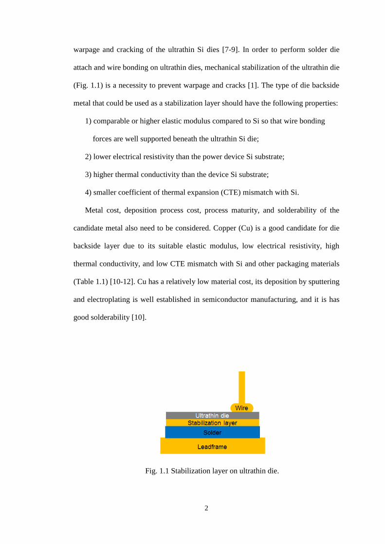
warpage and cracking of the ultrathin Si dies [7-9]. In order to perform solder die
attach and wire bonding on ultrathin dies, mechanical stabilization of the ultrathin die
(Fig. 1.1) is a necessity to prevent warpage and cracks [1]. The type of die backside
metal that could be used as a stabilization layer should have the following properties:
1) comparable or higher elastic modulus compared to Si so that wire bonding
forces are well supported beneath the ultrathin Si die;
2) lower electrical resistivity than the power device Si substrate;
3) higher thermal conductivity than the device Si substrate;
4) smaller coefficient of thermal expansion (CTE) mismatch with Si.
Metal cost, deposition process cost, process maturity, and solderability of the
candidate metal also need to be considered. Copper (Cu) is a good candidate for die
backside layer due to its suitable elastic modulus, low electrical resistivity, high
thermal conductivity, and low CTE mismatch with Si and other packaging materials
(Table 1.1) [10-12]. Cu has a relatively low material cost, its deposition by sputtering
and electroplating is well established in semiconductor manufacturing, and it is has
good solderability [10].
Fig. 1.1 Stabilization layer on ultrathin die.

3
Table 1.1 Mechanical, thermal and electrical properties of some elements [10-12].
CTE
(ppm/K)
Electrical
resistivity
( Ωm)
Thermal
conductivity
(W/cmK)
Elastic
modulus
(GPa)
Melting point
(ºC)
Si 2.6 1000-10000 1.5 130-169 1960
Cu 16.5 1.7 4.0 120 1085
Al 23.1 2.7 2.4 70 660
Ni 13.4 7.2 0.9 200 1455
Ag 18.9 1.6 4.3 83 962
Ti 8.6 39 0.2 110 1668
Cr 4.9 12.7 0.9 279 1907
Pt 8.8 10.8 0.7 168 1768
Pd 11.8 10.8 0.7 121 1555
W 4.5 5.4 1.7 400 3422
Au 14.2 2.3 3.2 79 1064
The dicing of Si wafers with a backside Cu layer is challenging. Conventional
mechanical blade dicing is not recommended owing to blade clogging and damage
caused by the Cu layer, and the susceptibility of the ultrathin Si to cracks. Plasma
dicing is another dicing option but the cost is prohibitive owing to additional
photolithography steps and wet/plasma etching steps required due to different
materials in the dicing street. Laser dicing is promising and is currently used to
singulate thin Si wafers [1] but there is no reported work of its application for dicing
ultrathin Si with Cu layer simultaneously. The mechanical strength of ultrathin dies
is very important to prevent die cracks during manufacturing processes and field
applications [1]. The effect of nanosecond laser dicing on the ultrathin die
mechanical strength, the fracture mechanism, and laser-induced die sidewall defects
are reported in this research work. The methodologies and challenges for stress
analysis of the composite structure of the ultrathin Si die, where the thicknesses of

4
the Cu layers are significant compared to the Si, are also discussed. From the current
findings, proposals for future research work are made.
1.2 Research objectives
The main objectives of this research work are:
1) To investigate the effect of nanosecond laser dicing on the mechanical
strength of ultrathin Si dies sandwiched between frontside and backside Cu
layers.
2) To determine the fracture mechanism of the ultrathin Si dies during
mechanical strength testing.
3) To study the effect of nanosecond laser dicing on the ultrathin Si die sidewall
structure, defects and composition.
1.3 Research originality
Currently, there is no reported work in the literature on the fabrication of
ultrathin dies with thick frontside and backside Cu layers, and its mechanical and
material properties [1]. As laser dicing is a promising option for the singulation of
ultrathin wafers with thick backside Cu layer, research is required on the effect of the
thick Cu layer during laser dicing, and the resulting mechanical and material
properties of the ultrathin die. This research work shows the feasibility of laser
dicing 20 µm Si dies with 10-30 µm backside Cu with nanosecond ultraviolet (UV)
laser. Die sidewall microstructural defects, morphologies, and phases have been
characterized in detail by transmission electron microscopy (TEM). After
nanosecond laser dicing, a higher density of defects and a deeper heat affected zone
(HAZ) in the sidewall region near the die frontside were found, compared with the
5
sidewall region near the die backside. The TEM findings agree well with three-point
bend (3PB) measurements where the die frontside characteristic fracture load was
lower than the die backside characteristic fracture load. A new analytical method for
3PB stress analysis in the ultrathin die was also explored because of the composite
Si/Cu structure of the ultrathin die. The classical equation for the maximum 3PB
tensile stress in a simple Si die cannot be used [15]. As such, new 3PB stress
equations were derived in this work to analyze the stresses in the composite structure
of the die. Apart from that, fractographic analysis showed that the 3PB test
measurements were sensitive to the laser-induced Si die sidewall damage and were
not sensitive to the Si die backside surface. This was an important finding to validate
that the 3PB test is suitable for characterizing the effect of laser dicing on the die
mechanical strength.
1.4 Scope of study
This research work involves the fabrication of 20 µm Si dies with 5, 10 and
20 µm frontside Cu and 10, 20 and 30 µm backside Cu as a stabilization layer. The
thinning of the Si wafers was carried out by precision backgrinding, in which the
wafers were temporarily mounted on rigid glass carriers using an adhesive. The Cu
layer deposition was done through a combination of sputtering and electroplating.
The detailed wafer thinning and metal depositon methods will be described in future
chapters. The cross-sectional structure and interfaces of the ultrathin dies were
investigated with materialographic sectioning, optical microscopy and scanning
electron miscoscopy (SEM).
In this work, laser with 35 ns pulsewidth and 355 nm wavelength (UV) was
used. Various characterization methods were used to study the effect of the laser. The
6
effect of laser dicing on the mechanical strength of the die sidewall was investigated
by 3PB test. Separate 3PB testing was done with loading on the die frontside and
backside. This is to determine the difference in the die frontside and backside
fracture strengths. Weibull analysis was utilized to determine the characteristic die
frontside and backside fracture loads from the 3PB test data. Stress analysis by
analytical method was carried out to determine the maximum tensile stress in the Si.
As the classical stress equation for 3PB test is not valid for a composite die structure,
new stress equations for the maximum stresses were derived from first principles.
Fractographic analysis by SEM was done on the 3PB samples to determine the
fracture initiation site and mechanism. The die sidewall defect morphologies,
structures and elemental compositions were then characterized in detail by TEM.
Finally, the TEM findings were studied to understand the effect of the die sidewall
defects on the die sidewall strengths at the die frontside and backside as indicated by
the 3PB test.
1.5 Organization of thesis
This thesis is divided into six chapters to elaborate the content of this work in
detail. After a brief introduction in this chapter, a review of current literature will be
presented in Chapter 2.
Following that, the materials and working principles of the instruments used
in the fabrication of ultrathin wafers and dies with Cu stabilization layer will be
presented in detail in Chapter 3. Besides that, the working principles behind the
instruments used for characterization of the ultrathin dies will also be discussed
briefly. In Chapter 4, the ultrathin wafer and die fabrication procedures will be
presented. Subsequently, the ultrathin die characterization methodology will be

7
discussed. In Chapter 5, the results of materialographic analysis, mechanical strength
testing, stress analysis, fractographic analysis and die sidewall defect analysis of the
ultrathin dies will be presented and discussed. Finally, Chapter 6 provides the
conclusions of the entire work and a brief discussion on the potential direction for
future research study on laser dicing of ultrathin wafer with Cu stablization layer.
8
CHAPTER 2
LITERATURE REVIEW
2.1 Introduction
This chapter is a brief review of ultrathin wafer fabrication and wafer dicing
technologies. The review on ultrathin wafer fabrication technology covers wafer
carriers systems, wafer backgrinding and wafer post-grinding treatment. The review
on wafer dicing technologies covers mechanical blade dicing, laser dicing and
plasma dicing.
2.2 Wafer carrier systems
2.2.1 Carrier systems with temporary bonding/debonding
Temporary wafer bonding and debonding have emerged as critical enabling
processes for ultrathin wafer thinning [16-24]. This approach involves temporarily
bonding a rigid and flat support carrier to the wafer before backgrinding. The carrier
could be made of silicon, ceramic, or glass. For bonding the wafer to the carrier,
temporary adhesives are used, so that the thinned wafer could be separated from the
support carrier at the end of the process flow.
The major requirements of temporary adhesives are related to its process flow,
thermal stability, chemical resistance, and mechanical strength [20]. Thermal
stability should allow high temperature processing up to 400ºC for dielectric
deposition, metal deposition, polymer curing, solder reflow, metal sintering, or other
high temperature processes. The adhesive must be resistant to the chemicals used in
the process flow e.g. water, solvents, acidic/base chemistries, and plasma chemistries.

9
Mechanical strength is required to hold the thin wafer rigidly during
processing, especially during backgrinding. Hermanowski [18] reported that the
mechanical properties of the adhesive, as well as the backgrinding process
parameters, need to be matched in order to obtain the optimum backgrinding quality
and material removal rate. Table 2.1 shows an overview of desired material and
process properties for temporary adhesives and support carriers.
Table 2.1 Desired properties of temporary adhesives and support carriers [18-20,22].
Among all the concerns for temporary adhesives, the thermal stability is the
highest because major issues have been reported to occur after high temperature
processing [18-20,25]. The thermal stability of temporary adhesives is dependent
upon its ability to resist decomposition and outgassing during exposure to high
process temperatures. The commonly reported adhesive failure modes after exposure
to high temperatures are: complete delamination of the thinned wafer from the carrier;
localized delamination of the thinned wafer in the form of gas pockets [18-19]; and
flower-shaped delamination defects [25]. These defects occur during high
temperature and high vacuum processing indicating that the pressure of the volatile
decomposition products is enhanced by the high vacuum. Therefore high temperature

10
characterization of temporary adhesives for thermal decomposition and outgassing
using methods such as thermogravimetric analysis (TGA) will be helpful in selecting
the proper type of adhesive for a specific process temperature budget [18,24].
Saito et al. [26] found that the carrier flatness has a significant effect on total
thickness variation (TTV) performance. In their study, it was found that each glass
carrier has its own surface topography with 30-40 µm of flatness. When a glass
carrier with 300 mm diameter is held down on a vacuum chuck, it has a more
uniform thickness within a diameter of roughly 200 mm and lower thickness towards
the outer edge by about 1.0 µm. Since the glass carrier is placed in direct contact
with the uncured liquid adhesive layer, this can affect the TTV. An attempt to correct
the distortion of the glass carrier was conducted using a flatting disk made of 25 mm
thick boro-silicate glass with vacuum groove. Immediately after wafer bonding is
done, the flatting disk is placed onto a carrier glass and vacuum is applied through
the vacuum groove along the outer edge of the glass, then UV light is irradiated
through the flatting disk to cure the adhesive while the flatting disk holds the carrier
glass flat (Fig. 2.1). The flatting disk also adds pressure by its weight of
approximately 6 kg over the entire surface of the glass carrier. However, there is no
significant change of adhesive thickness due to the pressure. With the flatting disk,
the TTV distribution has been improved from a worst case of ~9 µm to ~4 µm.
Fig. 2.1 Flatting disk applied on a carrier glass [26].

11
Data suggest that carrier plates with better flatness can improve TTV. Beyne
[21-22] reported a TTV of 1.6 µm for a 300 mm thinned to 50 µm thickness using a
silicon carrier. It was mentioned that silicon carriers are preferred because they have
a comparable flatness to precision-ground glass carriers which are significantly
higher in cost than silicon carriers. Also, silicon carriers have other advantages such
as better CTE matching to silicon device wafer, compatibility to electrostatic chucks,
high thermal and electrical conductivity, and is highly compatible to semiconductor
equipment, although it is not optically transparent and is not compatible with laser-
based adhesive curing and debonding.
Kitaichi et al. [27] achieved a TTV of 1.0 µm for 300 mm wafers thinned to
10 µm thickness. To achieve the target silicon wafer TTV specification, individual
targets must be set for the TTV accuracy of the glass carrier, adhesive layer, and
silicon wafer. Kitaichi et al. [27] improved the glass thickness accuracy by working
with the glass manufacturer. The silicon wafer/adhesive/glass carrier stack thickness
accuracy was improved by optimizing the flatting disk diameter and load pressure.
This minimizes the adhesive thickness difference in the wafer center compared to the
wafer edge due to adhesive squeeze-out at the wafer edge.
There are three main temporary wafer bonding/debonding and adhesive
systems for ultrathin wafer handling in the market: Wafer Support System (WSS)
[28], WaferBOND HT10.10 [29], and T-MAT [30]. These temporary wafer
bonding/debonding systems are described below.

12
2.2.1(a) Wafer Support System (WSS)
This process uses a room temperature UV-curable acrylic adhesive coated on
the wafer and joined to a laser absorbing adhesive layer coated on a glass carrier.
During spin coating, the adhesive flows into the topography of the wafer frontside,
providing overall support even on wafers with large flip-chip bumps. The laser
absorbing material is known as light-to-heat conversion (LTHC) material.
Debonding can occur after the wafer stack is attached to a dicing tape frame with the
thinned wafer attached to the tape. A laser then irradiates the stack through the glass
side allowing easy removal of the glass carrier. The thinned wafer remains constantly
supported by and attached to the dicing tape frame. The adhesive remaining on the
thinned wafer is removed by a peeling process using detaping tape. The adhesive
does not require cleaning after debonding. The overall process is shown in Fig. 2.2.
The use of the LTHC layer allows the selection and tuning of an adhesive based on
the needs of the process. Higher adhesive thermal stability can be achieved while
maintaining a low temperature and low stress method to remove the carrier.
Fig. 2.2 WSS process flow [28].

13
2.2.1(b) WaferBOND HT10.10
This process uses an adhesive cast in solvent which is spin coated and baked
similar to photoresist. Bonding is done in a vacuum chamber at moderate force (~15
psi) and at ~180ºC. Debonding is conducted using a thermal-slide process where the
wafer stack is heated and the thinned wafer is slid off the carrier wafer using a lateral
force. The thinned wafer must then be cleaned using a solvent to remove the residue
of the adhesive as shown in Fig. 2.3.
HT10.10 is one of several materials, including waxes, high temperature
polyimide (HD3007), and other thermoplastic polymers that can be debonded using a
thermal slide approach. The bond process for these adhesives is simple and can be
done on most bonders. The debond process is much more complicated when
compared to other temporary adhesive systems. The challenging part is supporting
the thinned wafer with an electrostatic chuck during the thermal slide and subsequent
solvent cleaning without breaking the thinned wafer.
Fig. 2.3 WaferBOND HT10.10 process flow [29].

14
2.2.1(c) T-MAT
This process uses a precursor spun on to the wafer. This is then converted via
a simple plasma-enhanced chemical vapor deposition (PE-CVD) process to form a
release layer ~100-150 nm thick. The elastomer used is a high temperature material
cured at ~180ºC which joins the wafer to the carrier. Debonding can occur after the
wafer stack is attached to a dicing tape frame with the thinned wafer attached to the
tape. One vacuum chuck is used to hold the thinned wafer via the taped side while
another holds the carrier. Upon slight separation of the stack at one side, a debonding
wave moves through the stack, leaving behind the thinned wafer supported by the
tape frame. The process is shown in Fig. 2.4.
Fig. 2.4 T-MAT process flow [30].
The release layer allows the separation of the adhesive thermal and
mechanical properties. The release layer also creates a situation where the holding
force of the adhesive is very strong in the plane of the wafer but much weaker and
adjustable in the direction perpendicular to its surface. These properties allow room
15
temperature debonding, high temperature stability adhesive, and reliable support of
the thinned wafer throughout the entire process.
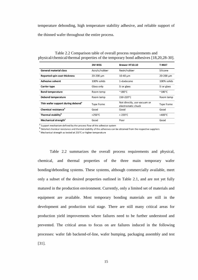
Table 2.2 Comparison table of overall process requirements and
physical/chemical/thermal properties of the temporary bond adhesives [18,20,28-30].
Table 2.2 summarizes the overall process requirements and physical,
chemical, and thermal properties of the three main temporary wafer
bonding/debonding systems. These systems, although commercially available, meet
only a subset of the desired properties outlined in Table 2.1, and are not yet fully
matured in the production environment. Currently, only a limited set of materials and
equipment are available. Most temporary bonding materials are still in the
development and production trial stage. There are still many critical areas for
production yield improvements where failures need to be further understood and
prevented. The critical areas to focus on are failures induced in the following
processes: wafer fab backend-of-line, wafer bumping, packaging assembly and test
[31].
16
2.3 Wafer backgrinding
Usually, back grinding is carried out in two steps: coarse grinding and fine
grinding. Coarse grinding employs a coarse grinding wheel with larger diamond
abrasives to remove most of the total thickness reduction required, as well as a faster
feed rate to achieve higher manufacturing throughput. Usually, the subsurface
damage (SSD) induced by coarse grinding (consisting of polycrystalline layer,
microcracks, dislocations, and residual stresses) is excessive and has to be removed
by a fine grinding step. For fine grinding, a slower feed rate and a fine grinding
wheel with smaller diamond abrasives are used to remove a small amount of silicon
(typically 10 to 30 µm).
2.3.1 Types of backgrinding
There are three types of grinders developed for backgrinding applications i.e.
Blanchard type, creep-feed type, and in-feed type. Earlier backgrinders used in the
semiconductor industry are of Blanchard type and creep-feed type [11,33-34]. Fig.
2.5 illustrates the Blanchard type grinder. A rotary table has multiple chucks aligned
along a circle, and each chuck holds a silicon wafer, where wafers do not rotate
around their own centres. A grinding wheel of a cup shape has a diameter larger than
the wafer diameter. The rotation axis of the grinding wheel is located on the circle
along which the centres of the wafers are aligned. During grinding, the rotary table
feeds the wafers to the rotating wheel. The rotating wheel also moves toward the
table surface at a certain feed rate. It usually takes a large number of revolutions of
the rotary table to remove a required thickness of silicon from the wafer surfaces.

17
Fig. 2.5 Blanchard type wafer backgrinding.
Similar to Blanchard type grinders, a creep-feed grinder has a rotary table
with multiple chucks with each holding a wafer, where wafers do not rotate about
their own centres. A major difference is that for creep-feed grinders, several
(typically three) grinding wheels of a cup shape are used and each rotates around its
own axis. These wheels can have different diamond grain sizes ranging from coarse
to fine. For example, three wheels can have grain sizes of mesh #320, #600, and
#1700, respectively [34]. These wheels have a diameter larger than the wafer
diameter. The rotation axes of the grinding wheels are located on the circle along
which the centres of the wafers are aligned. During grinding, the rotary table feeds
the wafer horizontally to the rotating grinding wheels. The grinding wheels are
positioned above the rotating table in a way that the cutting surfaces of these
grinding wheels will be at progressively lower positions relative to the table surface.
For example, if a total of 100 µm needs to be removed from the wafer backside
surfaces, the three wheels can grind thicknesses of 70 µm, 20 µm, and 10 µm,
respectively [34]. To achieve this when the rotary table has multiple wafers, at least

18
one of the spaces between two adjacent wafers needs to be large enough to fit three
grinding wheels. Through one rotation of the table, a desired total thickness of silicon
is removed from each wafer surface.
For creep-feed grinding, since the wafers are finished through one rotation of
the table, the grinding wheels rotate faster and the table rotates slower than in
Blanchard type grinding [34]. Compared to Blanchard type grinders, creep-feed
grinders have better control over the target thickness of ground wafers and produce
wafers with lower warpage values [34]. Both Blanchard type and creep-feed wafer
grinders have high manufacturing throughput. However, they both produce poor
TTV on ground wafers. As illustrated in Fig. 2.6, the contact length (L) between the
grinding wheel and the silicon wafer changes at every moment. Because the grinding
force is nearly inversely proportional to the contact length, it also varies at every
moment, causing wafer thickness to vary from thin to thick to thin along the feed
direction [32,35].
Fig. 2.6 Contact length between grinding wheel and silicon wafer in Blanchard type
and creep-feed wafer grinding [35].
19
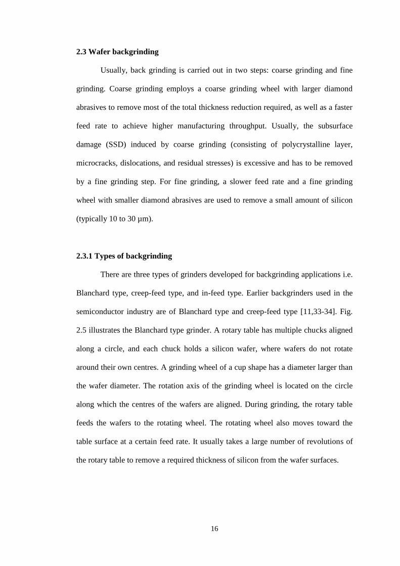
Subsequently, another type of backgrinding machine called an in-feed wafer
grinder was developed [32,35-37] with capability of producing better TTV on ground
wafers. Fig. 2.7 illustrates this type of wafer grinder. The wafer is held on a porous
ceramic chuck by means of a vacuum. During grinding, both the grinding wheel and
the wafer rotate about their own axes simultaneously, and the wheel is fed towards
the wafer along its axis. The rotation axis for the grinding wheel is offset by the
length of the wheel radius relative to the rotation axis for the wafer. Because the
contact length between the grinding wheel and silicon wafer is constant, the TTV of
wafers ground by in-feed grinders is significantly improved [35].
Fig. 2.7 In-feed type wafer backgrinding where is the feed rate, ω1 is the chuck
rotational speed and ω2 is the wheel rotational speed.
The TTV of ultrathin wafers after grinding is determined by the contact angle
between the grinding wheel and silicon wafer surface [38-40]. The thickness
variations in the wafer, glass carrier, and temporary adhesive have an influence on
the contact angle. Disco developed an automatic wafer thickness uniformity feedback
process for improving TTV (auto-TTV) especially for ultrathin wafers [39-40]. Fig.

20
2.8 explains auto-TTV process. After grinding some amount of Si wafer, the initial
TTV is measured using a non-contact gauge (NCG). By using the initial TTV,
adjustment of contact angle is carried out automatically before the final backgrind,
consequently giving an improved TTV. Kim et al. [40] claim to have achieved a
TTV of 0.5 µm for a 300 mm wafer thinned to 7 µm thickness by utilizing auto-TTV
and NCG. Current NCG probe silicon thickness resolution is 0.003 µm to 0.2 µm
[41]. NCG probe technology still needs to be improved for silicon with high doping
level (power devices, microelectromechanical system (MEMS), etc) and wafer
thicknesses below 55 µm.
Fig. 2.8 Auto-TTV process for improving total thickness variation of silicon wafer
[40].

21
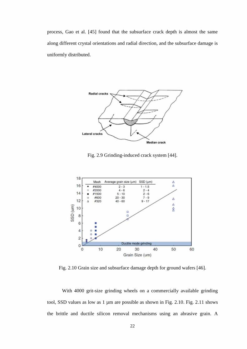
2.3.2 Subsurface damage control
Microcrack configurations caused by indentation and grinding of silicon have
been studied by various workers [42-45]. Median, radial and lateral cracks have been
reported as the major crack types when machining brittle materials as shown in Fig.
2.9. Pei et al. [44] found that for (100) silicon wafers, grinding-induced subsurface
cracks exhibit six configurations: median, lateral, umbrella, chevron, branch, and
fork. The umbrella cracks can be considered consisting of two lateral cracks and one
median crack. Radial cracks were not observable with the sample preparation method
used by Pei et al. [44] because the samples were taken in such a way that the
observed surface is perpendicular to the grinding direction while the radial cracks are
also perpendicular to the grinding direction. In general, it was found that larger grit
size resulted in deeper cracks and SSD [42,44-46]. Lundt et al. [46] and Pei et al. [44]
have shown that the SSD depth depends linearly on the size of the diamond grain in
the grinding wheel (Fig. 2.10). The depth of subsurface cracks on ground silicon
wafers have been found to be approximately equal to one third [42] to half [44] of
the diamond grain size used in the grinding wheel.
Gao et al. [45] showed that on ground (100) silicon wafers without a spark-
out process, the subsurface crack depth in <110> crystal orientation is larger than
that in <100> crystal orientation and the subsurface crack depth gradually increases
along the radial direction from the center to the edge. In the spark-out process, done
as a final step of backgrinding, the wafer surface is being continuously removed
without resetting the depth of cut and the cutting force between the grinding wheel
and wafer is gradually reduced [45]. The larger subsurface crack in <110> crystal
orientation was due to crack initiation into the 111 crystal plane which has the
lowest covalent binding force in silicon. However, in ground wafers with spark-out
22
process, Gao et al. [45] found that the subsurface crack depth is almost the same
along different crystal orientations and radial direction, and the subsurface damage is
uniformly distributed.
Fig. 2.9 Grinding-induced crack system [44].
Fig. 2.10 Grain size and subsurface damage depth for ground wafers [46].
With 4000 grit-size grinding wheels on a commercially available grinding
tool, SSD values as low as 1 µm are possible as shown in Fig. 2.10. Fig. 2.11 shows
the brittle and ductile silicon removal mechanisms using an abrasive grain. A

23
submicron SSD range can be reached with ductile mode grinding. If the average
depth-of-cut dg of the diamond grains does not exceed a critical cutting depth dc, the
material can be removed without brittle fracture and the SSD consists mainly of
dislocation defects [42,45-48]. For single crystal silicon a dc value of 0.1 µm was
reported by Puttick [47]. Sharp et al. [48] have analyzed the dg in plunge grinding
(where the grinding wheel moves radially toward the work) using computer
simulation and an analytic model. Based on the analytic model from Sharp et al. [48],
Fig. 2.11 Silicon removal mechanisms: (a) brittle mode and (b) ductile mode [42].
the relationship between dg and grinding parameters (Fig. 2.7) was rewritten for
wafer grinding by Young et al. [42] as follows:
where R is half the grain size, is the feed rate in µm/min, is the distance from
wafer center to the sample location, ω1 is the chuck rotational speed in rpm, w2 is the

24
thickness of the diamond cup wheel, ω2 is the wheel rotational speed in rpm, Fυ is the
grain volume fraction in the binder and L is the mean circumference of the grinding
wheel. The maximum depth of subsurface cracks is related to dg and can be
minimized by using finer grain size, lower feed rate, lower chuck rotational speed,
and higher wheel rotational speed. However, due to grinding machine resonance and
thermal expansion at higher wheel rotational speeds (above 1200 rpm), the maximum
depth of subsurface cracks is deeper than predicted by Eq. (2.1) [42].
2.4 Wafer post-grinding treatment methods
Mechanical grinding provides a fast removal rate for silicon but results in a
subsurface damage region about 20 µm deep and a rough surface typically with a rms
roughness in the order of 2 µm. Therefore, the coarse grinding (thinning rate of ~5
µm/s) is usually followed by a fine grinding step (thinning rate ≤1 µm/s), which
removes most of the damage created by the coarse grinding step and reduces the
roughness to a few nanometers depending on the wheel combination applied [49]. To
further polish the surface and remove the SSD layer that remains after fine grinding,
an additional post-grinding process is required. Post-grinding process by wet etching
for backgrind damage removal and stress-relief will be reviewed in this section.
2.4.1 Wet etching
The chemistry most commonly used for isotropic wet etching of silicon is a
combination of nitric acid and hydrofluoric acid. It is very often referred to as the
HNA system (HF:Nitric:Acetic) with acetic acid added as a buffer for wet bench
applications. Nitric acid acts as an oxidizer to convert the silicon wafer surface into
silicon dioxide and then the HF acid etches (dissolves) the oxide. The following